Embed Size (px)
Citation preview
IntegratedCircuitSystems, Inc.
ICS94201
0428B- 11/28/05
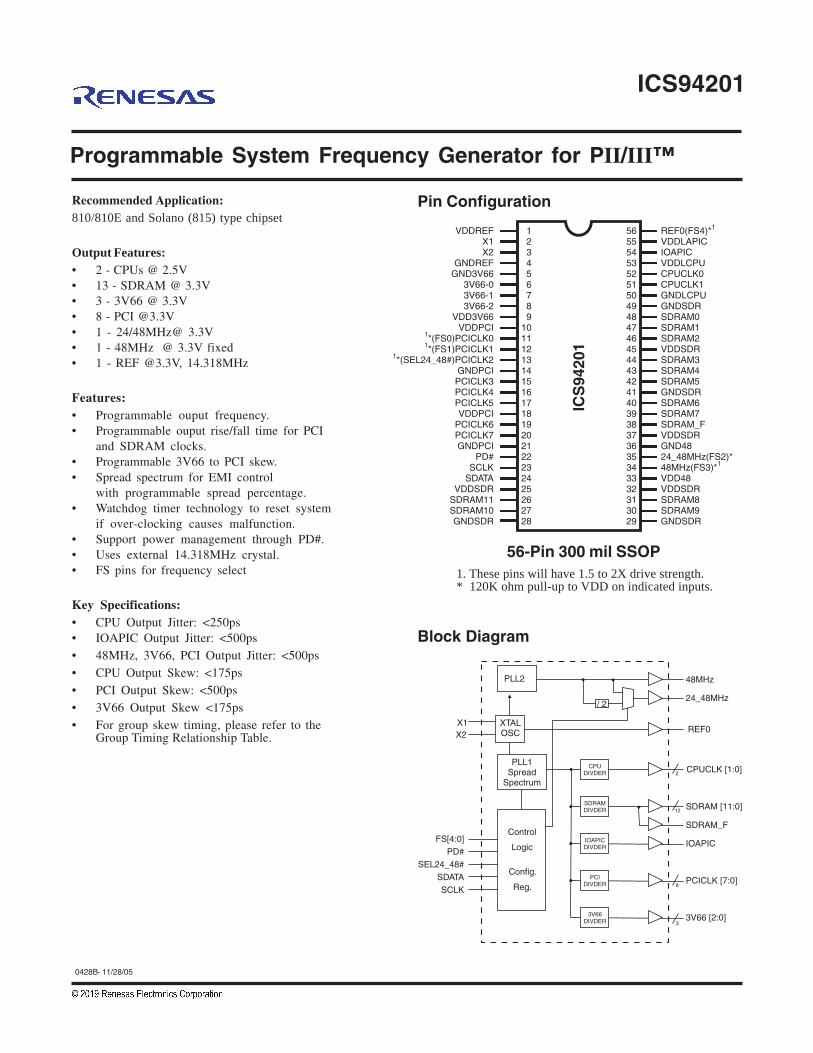
Pin ConfigurationRecommended Application:810/810E and Solano (815) type chipset
Output Features:• 2 - CPUs @ 2.5V• 13 - SDRAM @ 3.3V• 3 - 3V66 @ 3.3V• 8 - PCI @3.3V• 1 - 24/48MHz@ 3.3V• 1 - 48MHz @ 3.3V fixed• 1 - REF @3.3V, 14.318MHz
Features:• Programmable ouput frequency.• Programmable ouput rise/fall time for PCI
and SDRAM clocks.• Programmable 3V66 to PCI skew.• Spread spectrum for EMI control
with programmable spread percentage.• Watchdog timer technology to reset system
if over-clocking causes malfunction.• Support power management through PD#.• Uses external 14.318MHz crystal.• FS pins for frequency select
Key Specifications:• CPU Output Jitter: <250ps• IOAPIC Output Jitter: <500ps• 48MHz, 3V66, PCI Output Jitter: <500ps• CPU Output Skew: <175ps• PCI Output Skew: <500ps• 3V66 Output Skew <175ps• For group skew timing, please refer to the
Group Timing Relationship Table.
Programmable System Frequency Generator for PII/III™
56-Pin 300 mil SSOP1. These pins will have 1.5 to 2X drive strength.* 120K ohm pull-up to VDD on indicated inputs.
PLL2
PLL1Spread
Spectrum
48MHz
24_48MHz
CPUCLK [1:0]2
12
8
3
SDRAM [11:0]
IOAPIC
PCICLK [7:0]
SDRAM_F
3V66 [2:0]
X1X2
XTALOSC
CPUDIVDER
SDRAMDIVDER
IOAPICDIVDER
PCIDIVDER
3V66DIVDER
FS[4:0]PD#
SEL24_48#SDATASCLK
Control
Logic
Config.
Reg.
/ 2
REF0
Block Diagram
VDDREFX1X2
GNDREFGND3V66
3V66-13V66-2
VDD3V66VDDPCI
*(FS0)PCICLK0*(FS1)PCICLK1
*(SEL24_48#)PCICLK2GNDPCI
PCICLK3PCICLK4PCICLK5VDDPCI
PCICLK6PCICLK7GNDPCI
PD#SCLK
SDATAVDDSDR
SDRAM11SDRAM10GNDSDR
3V66-0
1
1
1
REF0(FS4)*VDDLAPICIOAPICVDDLCPUCPUCLK0CPUCLK1GNDLCPUGNDSDRSDRAM0SDRAM1SDRAM2VDDSDRSDRAM3SDRAM4SDRAM5GNDSDRSDRAM6SDRAM7SDRAM_FVDDSDRGND4824_48MHz(FS2)*48MHz(FS3)*VDD48VDDSDRSDRAM8SDRAM9GNDSDR
1
1
ICS
9420
1
123456789
10111213141516171819202122232425262728
56555453525150494847464544434241403938373635343332313029
2
ICS94201
0428B - 11/28/05
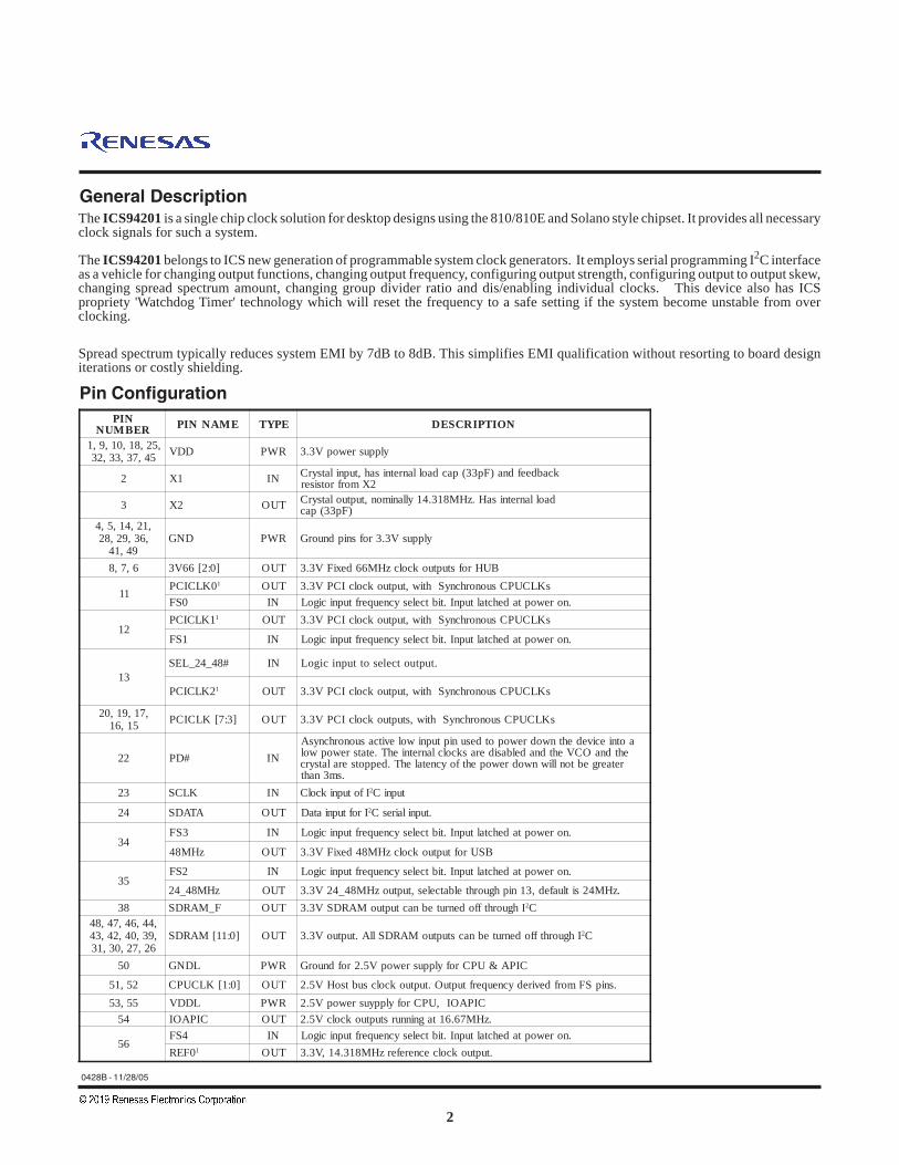
General Description
Pin Configuration
The ICS94201 is a single chip clock solution for desktop designs using the 810/810E and Solano style chipset. It provides all necessaryclock signals for such a system.
The ICS94201 belongs to ICS new generation of programmable system clock generators. It employs serial programming I2C interfaceas a vehicle for changing output functions, changing output frequency, configuring output strength, configuring output to output skew,changing spread spectrum amount, changing group divider ratio and dis/enabling individual clocks. This device also has ICSpropriety 'Watchdog Timer' technology which will reset the frequency to a safe setting if the system become unstable from overclocking.
Spread spectrum typically reduces system EMI by 7dB to 8dB. This simplifies EMI qualification without resorting to board designiterations or costly shielding.
NIPREBMUN EMANNIP EPYT NOITPIRCSED
,52,81,01,9,154,73,33,23 DDV RWP ylppusrewopV3.3
2 1X NI kcabdeefdna)Fp33(pacdaollanretnisah,tupnilatsyrC2Xmorfrotsiser
3 2X TUO daollanretnisaH.zHM813.41yllanimon,tuptuolatsyrC)Fp33(pac
,12,41,5,4,63,92,82
94,14DNG RWP ylppusV3.3rofsnipdnuorG
6,7,8 ]0:2[66V3 TUO BUHrofstuptuokcolczHM66dexiFV3.3
110KLCICP 1 TUO sKLCUPCsuonorhcnyShtiw,tuptuokcolcICPV3.3
0SF NI .norewoptadehctaltupnI.tibtcelesycneuqerftupnicigoL
211KLCICP 1 TUO sKLCUPCsuonorhcnyShtiw,tuptuokcolcICPV3.3
1SF NI .norewoptadehctaltupnI.tibtcelesycneuqerftupnicigoL
31#84_42_LES NI .tuptuotcelesottupnicigoL
2KLCICP 1 TUO sKLCUPCsuonorhcnyShtiw,tuptuokcolcICPV3.3
,71,91,0251,61 ]3:7[KLCICP TUO sKLCUPCsuonorhcnyShtiw,stuptuokcolcICPV3.3
22 #DP NIaotniecivedehtnwodrewopotdesuniptupniwolevitcasuonorhcnysA
ehtdnaOCVehtdnadelbasideraskcolclanretniehT.etatsrewopwolretaergebtonlliwnwodrewopehtfoycnetalehT.deppotseralatsyrc
.sm3naht32 KLCS NI IfotupnikcolC 2 tupniC
42 ATADS TUO IroftupniataD 2 .tupnilairesC
433SF NI .norewoptadehctaltupnI.tibtcelesycneuqerftupnicigoL
zHM84 TUO BSUroftuptuokcolczHM84dexiFV3.3
532SF NI .norewoptadehctaltupnI.tibtcelesycneuqerftupnicigoL
zHM84_42 TUO .zHM42sitluafed,31niphguorhtelbatceles,tuptuozHM84_42V3.383 F_MARDS TUO IhguorhtffodenrutebnactuptuoMARDSV3.3 2C
,44,64,74,84,93,04,24,34
62,72,03,13]0:11[MARDS TUO IhguorhtffodenrutebnacstuptuoMARDSllA.tuptuoV3.3 2C
05 LDNG RWP CIPA&UPCrofylppusrewopV5.2rofdnuorG
25,15 ]0:1[KLCUPC TUO .snipSFmorfdeviredycneuqerftuptuO.tuptuokcolcsubtsoHV5.255,35 LDDV RWP CIPAOI,UPCrofylppyusrewopV5.2
45 CIPAOI TUO .zHM76.61tagninnurstuptuokcolcV5.2
654SF NI .norewoptadehctaltupnI.tibtcelesycneuqerftupnicigoL
0FER 1 TUO .tuptuokcolcecnereferzHM813.41,V3.3
3
ICS94201
0428B - 11/28/05
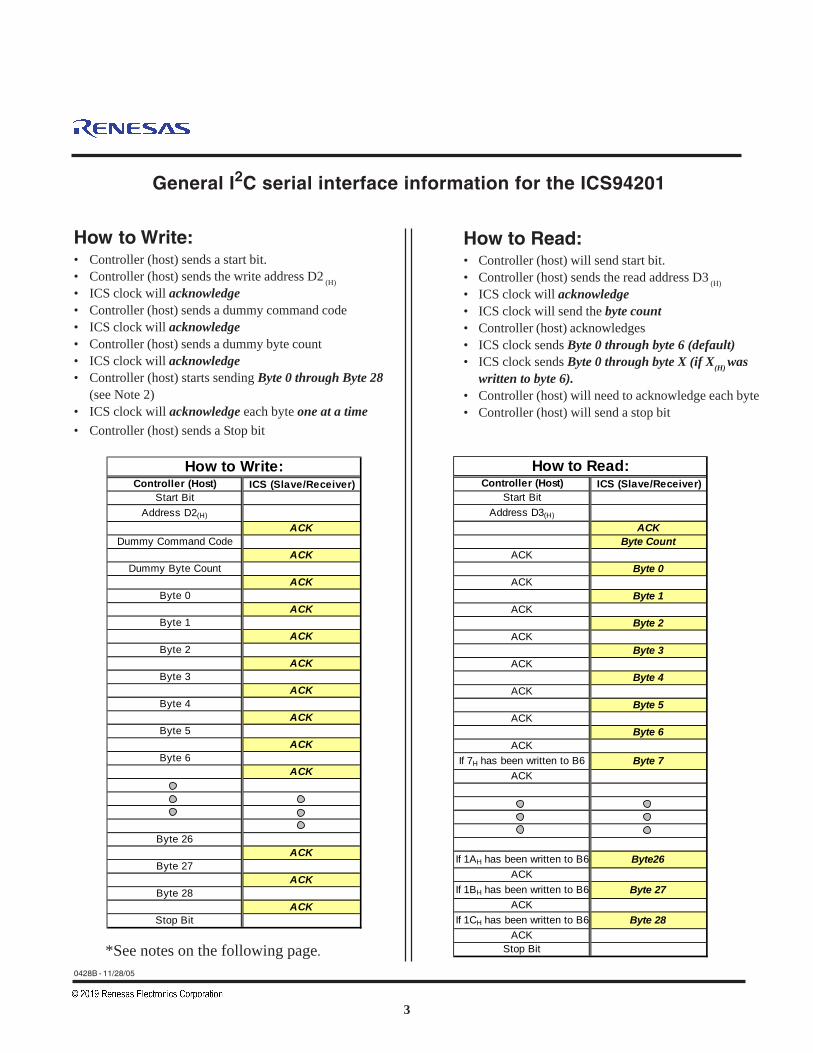
General I2C serial interface information for the ICS94201
How to Write:• Controller (host) sends a start bit.• Controller (host) sends the write address D2 (H)• ICS clock will acknowledge• Controller (host) sends a dummy command code• ICS clock will acknowledge• Controller (host) sends a dummy byte count• ICS clock will acknowledge• Controller (host) starts sending Byte 0 through Byte 28
(see Note 2)• ICS clock will acknowledge each byte one at a time• Controller (host) sends a Stop bit
How to Read:• Controller (host) will send start bit.• Controller (host) sends the read address D3 (H)• ICS clock will acknowledge• ICS clock will send the byte count• Controller (host) acknowledges• ICS clock sends Byte 0 through byte 6 (default)• ICS clock sends Byte 0 through byte X (if X(H) was
written to byte 6).• Controller (host) will need to acknowledge each byte• Controller (host) will send a stop bit
Controller (Host) ICS (Slave/Receiver)Start Bit
Address D2(H)
ACKDummy Command Code
ACKDummy Byte Count
ACKByte 0
ACKByte 1
ACKByte 2
ACKByte 3
ACKByte 4
ACKByte 5
ACKByte 6
ACK
Byte 26ACK
Byte 27ACK
Byte 28ACK
Stop Bit
How to Write:Controller (Host) ICS (Slave/Receiver)
Start BitAddress D3(H)
ACKByte Count
ACKByte 0
ACKByte 1
ACKByte 2
ACKByte 3
ACKByte 4
ACKByte 5
ACKByte 6
ACKIf 7H has been written to B6 Byte 7
ACK
If 1AH has been written to B6 Byte26ACK
If 1BH has been written to B6 Byte 27ACK
If 1CH has been written to B6 Byte 28ACK
Stop Bit
How to Read:
*See notes on the following page.
4
ICS94201
0428B - 11/28/05
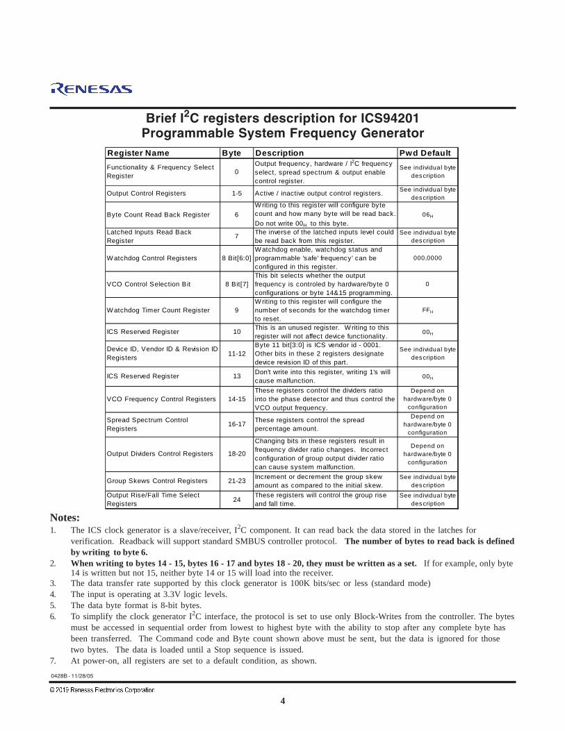
Notes:1. The ICS clock generator is a slave/receiver, I2C component. It can read back the data stored in the latches for
verification. Readback will support standard SMBUS controller protocol. The number of bytes to read back is definedby writing to byte 6.
2. When writing to bytes 14 - 15, bytes 16 - 17 and bytes 18 - 20, they must be written as a set. If for example, only byte14 is written but not 15, neither byte 14 or 15 will load into the receiver.
3. The data transfer rate supported by this clock generator is 100K bits/sec or less (standard mode)4. The input is operating at 3.3V logic levels.5. The data byte format is 8-bit bytes.6. To simplify the clock generator I2C interface, the protocol is set to use only Block-Writes from the controller. The bytes
must be accessed in sequential order from lowest to highest byte with the ability to stop after any complete byte hasbeen transferred. The Command code and Byte count shown above must be sent, but the data is ignored for thosetwo bytes. The data is loaded until a Stop sequence is issued.
7. At power-on, all registers are set to a default condition, as shown.
Register Name Byte Description Pwd Default Functionality & Frequency Select Register 0
Output frequency, hardware / I2C frequency select, spread spectrum & output enable control register.
See individual byte description
Output Control Registers 1-5 Active / inactive output control registers. See individual byte description
Byte Count Read Back Register 6W riting to this register will configure byte count and how many byte will be read back. Do not write 00H to this byte.
06H
Latched Inputs Read Back Register
7 The inverse of the latched inputs level could be read back from this register.
See individual byte description
W atchdog Control Registers 8 Bit[6:0]W atchdog enable, watchdog status and programmable 'safe' frequency' can be configured in this register.
000,0000
VCO Control Selection Bit 8 Bit[7]This bit selects whether the output frequency is controled by hardware/byte 0 configurations or byte 14&15 programming.
0
W atchdog Timer Count Register 9W riting to this register will configure the number of seconds for the watchdog timer to reset.
FFH
ICS Reserved Register 10 This is an unused register. W riting to this register will not affect device functionality. 00H
Device ID, Vendor ID & Revision ID Registers 11-12
Byte 11 bit[3:0] is ICS vendor id - 0001. Other bits in these 2 registers designate device revision ID of this part.
See individual byte description
ICS Reserved Register 13 Don't write into this register, writing 1's will cause malfunction. 00H
VCO Frequency Control Registers 14-15These registers control the dividers ratio into the phase detector and thus control the VCO output frequency.
Depend on hardware/byte 0
configuration
Spread Spectrum Control Registers
16-17 These registers control the spread percentage amount.
Depend on hardware/byte 0
configuration
Output Dividers Control Registers 18-20
Changing bits in these registers result in frequency divider ratio changes. Incorrect configuration of group output divider ratio can cause system malfunction.
Depend on hardware/byte 0
configuration
Group Skews Control Registers 21-23 Increment or decrement the group skew amount as compared to the initial skew.
See individual byte description
Output Rise/Fall Time Select Registers 24
These registers will control the group rise and fall time.
See individual byte description
Brief I2C registers description for ICS94201Programmable System Frequency Generator
5
ICS94201
0428B - 11/28/05
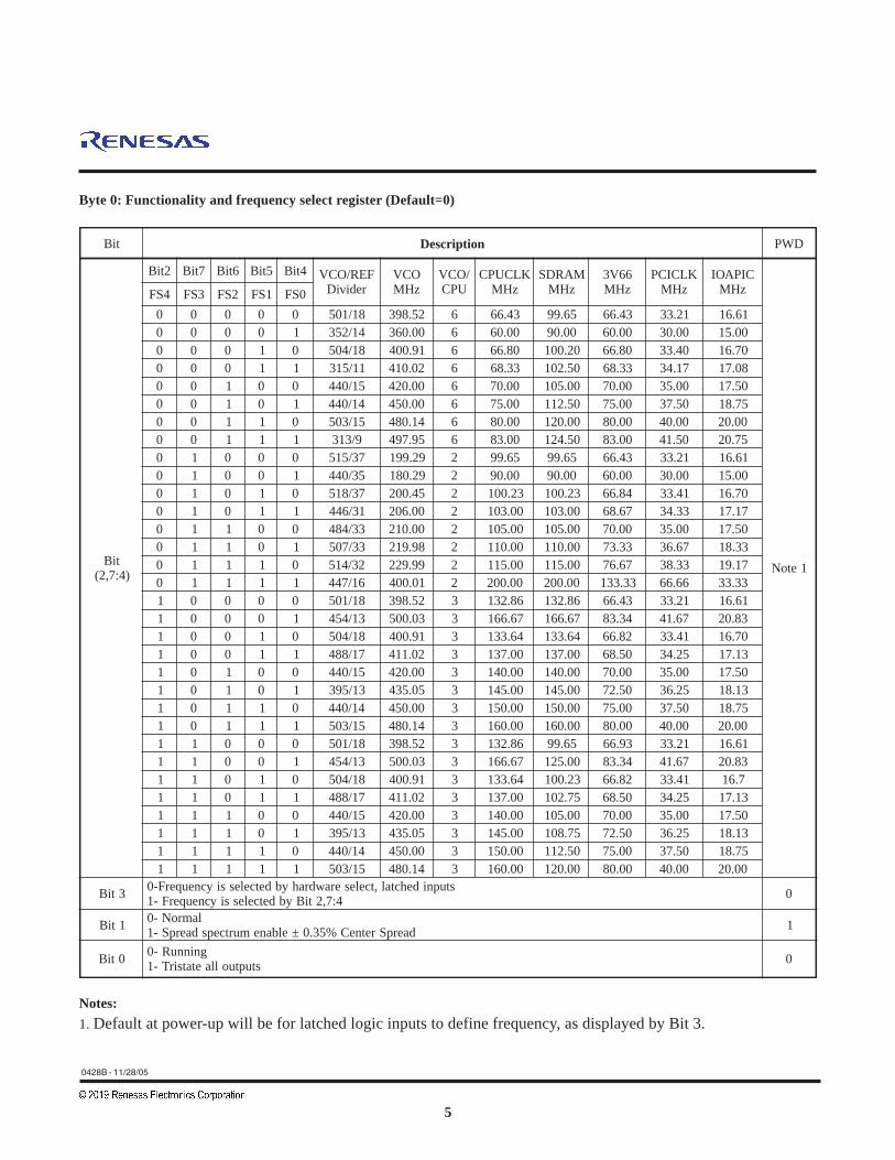
Byte 0: Functionality and frequency select register (Default=0)
Notes:1. Default at power-up will be for latched logic inputs to define frequency, as displayed by Bit 3.
tiB noitpircseD DWP
tiB)4:7,2(
2tiB 7tiB 6tiB 5tiB 4tiB FER/OCVrediviD
OCVzHM
/OCVUPC
KLCUPCzHM
MARDSzHM
66V3zHM
KLCICPzHM
CIPAOIzHM
1etoN
4SF 3SF 2SF 1SF 0SF0 0 0 0 0 81/105 25.893 6 34.66 56.99 34.66 12.33 16.610 0 0 0 1 41/253 00.063 6 00.06 00.09 00.06 00.03 00.510 0 0 1 0 81/405 19.004 6 08.66 02.001 08.66 04.33 07.610 0 0 1 1 11/513 20.014 6 33.86 05.201 33.86 71.43 80.710 0 1 0 0 51/044 00.024 6 00.07 00.501 00.07 00.53 05.710 0 1 0 1 41/044 00.054 6 00.57 05.211 00.57 05.73 57.810 0 1 1 0 51/305 41.084 6 00.08 00.021 00.08 00.04 00.020 0 1 1 1 9/313 59.794 6 00.38 05.421 00.38 05.14 57.020 1 0 0 0 73/515 92.991 2 56.99 56.99 34.66 12.33 16.610 1 0 0 1 53/044 92.081 2 00.09 00.09 00.06 00.03 00.510 1 0 1 0 73/815 54.002 2 32.001 32.001 48.66 14.33 07.610 1 0 1 1 13/644 00.602 2 00.301 00.301 76.86 33.43 71.710 1 1 0 0 33/484 00.012 2 00.501 00.501 00.07 00.53 05.710 1 1 0 1 33/705 89.912 2 00.011 00.011 33.37 76.63 33.810 1 1 1 0 23/415 99.922 2 00.511 00.511 76.67 33.83 71.910 1 1 1 1 61/744 10.004 2 00.002 00.002 33.331 66.66 33.331 0 0 0 0 81/105 25.893 3 68.231 68.231 34.66 12.33 16.611 0 0 0 1 31/454 30.005 3 76.661 76.661 43.38 76.14 38.021 0 0 1 0 81/405 19.004 3 46.331 46.331 28.66 14.33 07.611 0 0 1 1 71/884 20.114 3 00.731 00.731 05.86 52.43 31.711 0 1 0 0 51/044 00.024 3 00.041 00.041 00.07 00.53 05.711 0 1 0 1 31/593 50.534 3 00.541 00.541 05.27 52.63 31.811 0 1 1 0 41/044 00.054 3 00.051 00.051 00.57 05.73 57.811 0 1 1 1 51/305 41.084 3 00.061 00.061 00.08 00.04 00.021 1 0 0 0 81/105 25.893 3 68.231 56.99 39.66 12.33 16.611 1 0 0 1 31/454 30.005 3 76.661 00.521 43.38 76.14 38.021 1 0 1 0 81/405 19.004 3 46.331 32.001 28.66 14.33 7.611 1 0 1 1 71/884 20.114 3 00.731 57.201 05.86 52.43 31.711 1 1 0 0 51/044 00.024 3 00.041 00.501 00.07 00.53 05.711 1 1 0 1 31/593 50.534 3 00.541 57.801 05.27 52.63 31.811 1 1 1 0 41/044 00.054 3 00.051 05.211 00.57 05.73 57.811 1 1 1 1 51/305 41.084 3 00.061 00.021 00.08 00.04 00.02
3tiB stupnidehctal,tceleserawdrahybdetcelessiycneuqerF-04:7,2tiBybdetcelessiycneuqerF-1 0
1tiB lamroN-0daerpSretneC%53.0±elbanemurtcepsdaerpS-1 1
0tiB gninnuR-0stuptuollaetatsirT-1 0

6
ICS94201
0428B - 11/28/05
Byte 1: Output Control Register(1 = enable, 0 = disable)
Notes:1. Inactive means outputs are held LOW and are disabled from switching. These outputs are designed to be configured at
power-on and are not expected to be configured during the normal modes of operation.2. PWD = Power on Default
Byte 3: Output Control Register(1 = enable, 0 = disable)
Byte 2: Output Control Register(1 = enable, 0 = disable)
Byte 4: Output Control Register(1 = enable, 0 = disable)
Byte 5: Output Control Register(1 = enable, 0 = disable)
Byte 6: Byte Count Read Back Register
Note: Writing to this register will configure byte count andhow many bytes will be read back, default is 6 bytes.
tiB #niP DWP noitpircseD7tiB 93 1 7MARDS6tiB 04 1 6MARDS5tiB 24 1 5MARDS4tiB 34 1 4MARDS3tiB 44 1 3MARDS2tiB 64 1 2MARDS1tiB 74 1 1MARDS0tiB 84 1 0MARDS
tiB #niP DWP noitpircseD7tiB 8 1 2_66V36tiB 6 1 0_66V35tiB 7 1 1_66V34tiB - X #4SF3tiB 45 1 CIPAOI2tiB - X #1SF1tiB 15 1 1KLCUPC0tiB 25 1 0KLCUPC
tiB #niP DWP noitpircseD7tiB - 0 )etoN(devreseR6tiB - 0 )etoN(devreseR5tiB - 0 )etoN(devreseR4tiB - 0 )etoN(devreseR3tiB - 0 )etoN(devreseR2tiB - 1 )etoN(devreseR1tiB - 1 )etoN(devreseR0tiB - 0 )etoN(devreseR
tiB #niP DWP noitpircseD7tiB - 1 )devreseR(6tiB - 1 )devreseR(5tiB - 1 )devreseR(4tiB - 1 )devreseR(3tiB 62 1 11MARDS2tiB 72 1 01MARDS1tiB 03 1 9MARDS0tiB 13 1 8MARDS
tiB #niP DWP noitpircseD7tiB 02 1 7KLCICP6tiB 91 1 6KLCICP5tiB 71 1 5KLCICP4tiB 61 1 4KLCICP3tiB 51 1 3KLCICP2tiB 31 1 2KLCICP1tiB 21 1 1KLCICP0tiB 11 1 0KLCICP
tiB #niP DWP noitpircseD7tiB - X #3SF6tiB - X #0SF5tiB - X #2SF4tiB 53 1 zHM423tiB - 1 )devreseR(2tiB 43 1 zHM841tiB - 1 )devreseR(0tiB 83 1 F_MARDS
7
ICS94201
0428B - 11/28/05
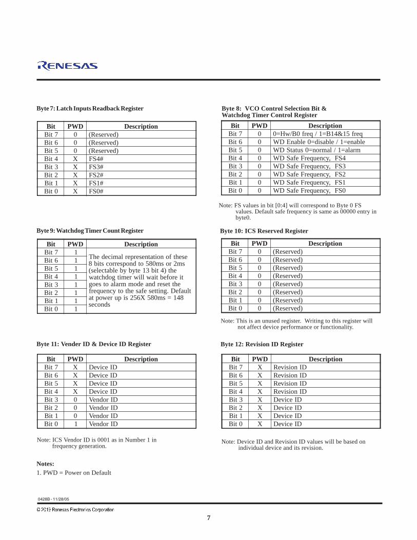
Byte 7: Latch Inputs Readback Register
Byte 9: Watchdog Timer Count Register
Byte 8: VCO Control Selection Bit &Watchdog Timer Control Register
Byte 10: ICS Reserved Register
Byte 11: Vender ID & Device ID Register Byte 12: Revision ID Register
Note: FS values in bit [0:4] will correspond to Byte 0 FSvalues. Default safe frequency is same as 00000 entry inbyte0.
Note: This is an unused register. Writing to this register willnot affect device performance or functionality.
Note: ICS Vendor ID is 0001 as in Number 1 infrequency generation.
Notes:1. PWD = Power on Default
tiB DWP noitpircseD7tiB 0 qerf51&41B=1/qerf0B/wH=06tiB 0 elbane=1/elbasid=0elbanEDW5tiB 0 mrala=1/lamron=0sutatSDW4tiB 0 4SF,ycneuqerFefaSDW3tiB 0 3SF,ycneuqerFefaSDW2tiB 0 2SF,ycneuqerFefaSDW1tiB 0 1SF,ycneuqerFefaSDW0tiB 0 0SF,ycneuqerFefaSDW
tiB DWP noitpircseD7tiB 0 )devreseR(6tiB 0 )devreseR(5tiB 0 )devreseR(4tiB 0 )devreseR(3tiB 0 )devreseR(2tiB 0 )devreseR(1tiB 0 )devreseR(0tiB 0 )devreseR(
tiB DWP noitpircseD7tiB X DInoisiveR6tiB X DInoisiveR5tiB X DInoisiveR4tiB X DInoisiveR3tiB X DIeciveD2tiB X DIeciveD1tiB X DIeciveD0tiB X DIeciveD
tiB DWP noitpircseD7tiB 0 )devreseR(6tiB 0 )devreseR(5tiB 0 )devreseR(4tiB X #4SF3tiB X #3SF2tiB X #2SF1tiB X #1SF0tiB X #0SF
tiB DWP noitpircseD7tiB 1
esehtfonoitatneserperlamicedehTsm2rosm085otdnopserrocstib8
eht)4tib31etybybelbatceles(tierofebtiawlliwremitgodhctaw
ehtteserdnaedommralaotseogtluafeD.gnittesefasehtotycneuqerf
841=sm085X652sipurewoptasdnoces
6tiB 15tiB 14tiB 13tiB 12tiB 11tiB 10tiB 1
tiB DWP noitpircseD7tiB X DIeciveD6tiB X DIeciveD5tiB X DIeciveD4tiB X DIeciveD3tiB 0 DIrodneV2tiB 0 DIrodneV1tiB 0 DIrodneV0tiB 1 DIrodneV
Note: Device ID and Revision ID values will be based onindividual device and its revision.

8
ICS94201
0428B - 11/28/05
Byte 13: ICS Reserved Register
Byte 15: VCO Frequency Control Register
Note: The decimal representation of these 9 bits (Byte 15 bit[7:0] & Byte 14 bit [7] ) + 8 is equal to the VCO divider value.For example if VCO divider value of 36 is desired, user needto program 36 - 8 = 28, namely, 0, 00011100 into byte 15 bit& byte 14 bit 7.
Note: DON'T write a '1' into this register, it willcause malfunction.
Byte 14: VCO Frequency Control Register
Note: The decimal representation of these 7 bits (Byte 14[6:0]) + 2 is equal to the REF divider value .
To program the VCO frequency for over-clocking.
0. Before trying to program our clock manually, consider using ICS provided software utilities for easy programming.
1. Select the frequency you want to over-clock from with the desired gear ratio (i.e. CPU:SDRAM:3V66:PCI ratio) by writing tobyte 0, or using initial hardware power up frequency.
2. Write 0001, 1001 (19H) to byte 6 for readback of 25 bytes (byte 0-24).
3. Read back byte 16-24 and copy values in these registers.
4. Re-initialize the write sequence.
5. Write a '1' to byte 8 bit 7 indicating you want to use byte 14 and 15 to control the VCO frequency.
6. Write to byte 14 & 15 with the desired VCO & REF divider values.
7. Write to byte 16 to 24 with the values you copy from step 3. This maintains the output divider mux controls the same gear ratio.
8. The above procedure is only needed when changing the VCO for the 1st pass. If VCO frequency needs to be changed again,user only needs to write to byte 14 and 15 unless the system is to reboot.
VCO Programming ConstrainsVCO Frequency ...................... 150MHz to 500MHzVCO Divider Range ................ 8 to 519REF Divider Range ................. 2 to 129Phase Detector Stability .......... 0.3536 to 1.4142Useful FormulaVCO Frequency = 14.31818 x VCO/REF divider valuePhase Detector Stabiliy = 14.038 x (VCO divider value)-0.5
tiB DWP noitpircseD7tiB X 8tiBrediviDOCV6tiB X 7tiBrediviDOCV5tiB X 6tiBrediviDOCV4tiB X 5tiBrediviDOCV3tiB X 4tiBrediviDOCV2tiB X 3tiBrediviDOCV1tiB X 2tiBrediviDOCV0tiB X 1tiBrediviDOCV
tiB DWP noitpircseD7tiB 0 )devreseR(6tiB 0 )devreseR(5tiB 0 )devreseR(
4tiB 0tcelesesabremit0W
sm085=0sm2=1
3tiB 0 )devreseR(2tiB 0 )devreseR(1tiB 0 )devreseR(0tiB 0 )devreseR(
tiB DWP noitpircseD7tiB X 0tiBrediviDOCV6tiB X 6tiBrediviDFER5tiB X 5tiBrediviDFER4tiB X 4tiBrediviDFER3tiB X 3tiBrediviDFER2tiB X 2tiBrediviDFER1tiB X 1tiBrediviDFER0tiB X 0tiBrediviDFER
9
ICS94201
0428B - 11/28/05
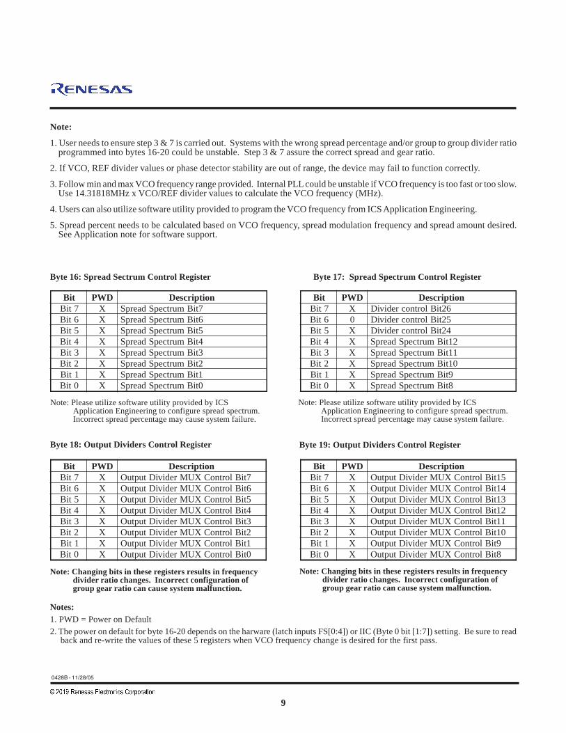
Byte 16: Spread Sectrum Control Register Byte 17: Spread Spectrum Control Register
Note: Please utilize software utility provided by ICSApplication Engineering to configure spread spectrum.Incorrect spread percentage may cause system failure.
Note: Please utilize software utility provided by ICSApplication Engineering to configure spread spectrum.Incorrect spread percentage may cause system failure.
Byte 18: Output Dividers Control Register Byte 19: Output Dividers Control Register
Note: Changing bits in these registers results in frequencydivider ratio changes. Incorrect configuration ofgroup gear ratio can cause system malfunction.
Note: Changing bits in these registers results in frequencydivider ratio changes. Incorrect configuration ofgroup gear ratio can cause system malfunction.
Notes:1. PWD = Power on Default2. The power on default for byte 16-20 depends on the harware (latch inputs FS[0:4]) or IIC (Byte 0 bit [1:7]) setting. Be sure to read
back and re-write the values of these 5 registers when VCO frequency change is desired for the first pass.
tiB DWP noitpircseD7tiB X 7tiBlortnoCXUMrediviDtuptuO6tiB X 6tiBlortnoCXUMrediviDtuptuO5tiB X 5tiBlortnoCXUMrediviDtuptuO4tiB X 4tiBlortnoCXUMrediviDtuptuO3tiB X 3tiBlortnoCXUMrediviDtuptuO2tiB X 2tiBlortnoCXUMrediviDtuptuO1tiB X 1tiBlortnoCXUMrediviDtuptuO0tiB X 0tiBlortnoCXUMrediviDtuptuO
tiB DWP noitpircseD7tiB X 51tiBlortnoCXUMrediviDtuptuO6tiB X 41tiBlortnoCXUMrediviDtuptuO5tiB X 31tiBlortnoCXUMrediviDtuptuO4tiB X 21tiBlortnoCXUMrediviDtuptuO3tiB X 11tiBlortnoCXUMrediviDtuptuO2tiB X 01tiBlortnoCXUMrediviDtuptuO1tiB X 9tiBlortnoCXUMrediviDtuptuO0tiB X 8tiBlortnoCXUMrediviDtuptuO
tiB DWP noitpircseD7tiB X 7tiBmurtcepSdaerpS6tiB X 6tiBmurtcepSdaerpS5tiB X 5tiBmurtcepSdaerpS4tiB X 4tiBmurtcepSdaerpS3tiB X 3tiBmurtcepSdaerpS2tiB X 2tiBmurtcepSdaerpS1tiB X 1tiBmurtcepSdaerpS0tiB X 0tiBmurtcepSdaerpS
tiB DWP noitpircseD7tiB X 62tiBlortnocrediviD6tiB 0 52tiBlortnocrediviD5tiB X 42tiBlortnocrediviD4tiB X 21tiBmurtcepSdaerpS3tiB X 11tiBmurtcepSdaerpS2tiB X 01tiBmurtcepSdaerpS1tiB X 9tiBmurtcepSdaerpS0tiB X 8tiBmurtcepSdaerpS
Note:
1. User needs to ensure step 3 & 7 is carried out. Systems with the wrong spread percentage and/or group to group divider ratioprogrammed into bytes 16-20 could be unstable. Step 3 & 7 assure the correct spread and gear ratio.
2. If VCO, REF divider values or phase detector stability are out of range, the device may fail to function correctly.
3. Follow min and max VCO frequency range provided. Internal PLL could be unstable if VCO frequency is too fast or too slow.Use 14.31818MHz x VCO/REF divider values to calculate the VCO frequency (MHz).
4. Users can also utilize software utility provided to program the VCO frequency from ICS Application Engineering.
5. Spread percent needs to be calculated based on VCO frequency, spread modulation frequency and spread amount desired.See Application note for software support.
10
ICS94201
0428B - 11/28/05
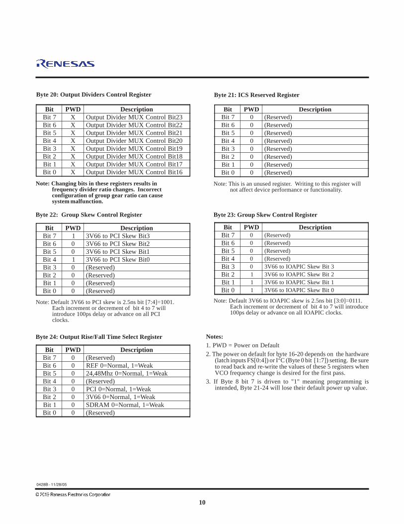
Byte 21: ICS Reserved Register
Byte 23: Group Skew Control RegisterByte 22: Group Skew Control Register
Note: Default 3V66 to PCI skew is 2.5ns bit [7:4]=1001.Each increment or decrement of bit 4 to 7 willintroduce 100ps delay or advance on all PCIclocks.
Byte 24: Output Rise/Fall Time Select Register
Note: This is an unused register. Writing to this register willnot affect device performance or functionality.
Byte 20: Output Dividers Control Register
Note: Changing bits in these registers results infrequency divider ratio changes. Incorrectconfiguration of group gear ratio can causesystem malfunction.
Notes:1. PWD = Power on Default2. The power on default for byte 16-20 depends on the hardware
(latch inputs FS[0:4]) or I2C (Byte 0 bit [1:7]) setting. Be sureto read back and re-write the values of these 5 registers whenVCO frequency change is desired for the first pass.
3. If Byte 8 bit 7 is driven to "1" meaning programming isintended, Byte 21-24 will lose their default power up value.
Note: Default 3V66 to IOAPIC skew is 2.5ns bit [3:0]=0111.Each increment or decrement of bit 4 to 7 will introduce100ps delay or advance on all IOAPIC clocks.
tiB DWP noitpircseD7tiB X 32tiBlortnoCXUMrediviDtuptuO6tiB X 22tiBlortnoCXUMrediviDtuptuO5tiB X 12tiBlortnoCXUMrediviDtuptuO4tiB X 02tiBlortnoCXUMrediviDtuptuO3tiB X 91tiBlortnoCXUMrediviDtuptuO2tiB X 81tiBlortnoCXUMrediviDtuptuO1tiB X 71tiBlortnoCXUMrediviDtuptuO0tiB X 61tiBlortnoCXUMrediviDtuptuO
tiB DWP noitpircseD7tiB 0 )devreseR(6tiB 0 )devreseR(5tiB 0 )devreseR(4tiB 0 )devreseR(3tiB 0 )devreseR(2tiB 0 )devreseR(1tiB 0 )devreseR(0tiB 0 )devreseR(
tiB DWP noitpircseD7tiB 1 3tiBwekSICPot66V36tiB 0 2tiBwekSICPot66V35tiB 0 1tiBwekSICPot66V34tiB 1 0tiBwekSICPot66V33tiB 0 )devreseR(2tiB 0 )devreseR(1tiB 0 )devreseR(0tiB 0 )devreseR(
tiB DWP noitpircseD7tiB 0 )devreseR(6tiB 0 kaeW=1,lamroN=0FER5tiB 0 kaeW=1,lamroN=0zhM84,424tiB 0 )devreseR(3tiB 0 kaeW=1,lamroN=0ICP2tiB 0 kaeW=1,lamroN=066V31tiB 0 kaeW=1,lamroN=0MARDS0tiB 0 )devreseR(
tiB DWP noitpircseD7tiB 0 )devreseR(6tiB 0 )devreseR(5tiB 0 )devreseR(4tiB 0 )devreseR(3tiB 0 3tiBwekSCIPAOIot66V32tiB 1 2tiBwekSCIPAOIot66V31tiB 1 1tiBwekSCIPAOIot66V30tiB 1 0tiBwekSCIPAOIot66V3
11
ICS94201
0428B - 11/28/05
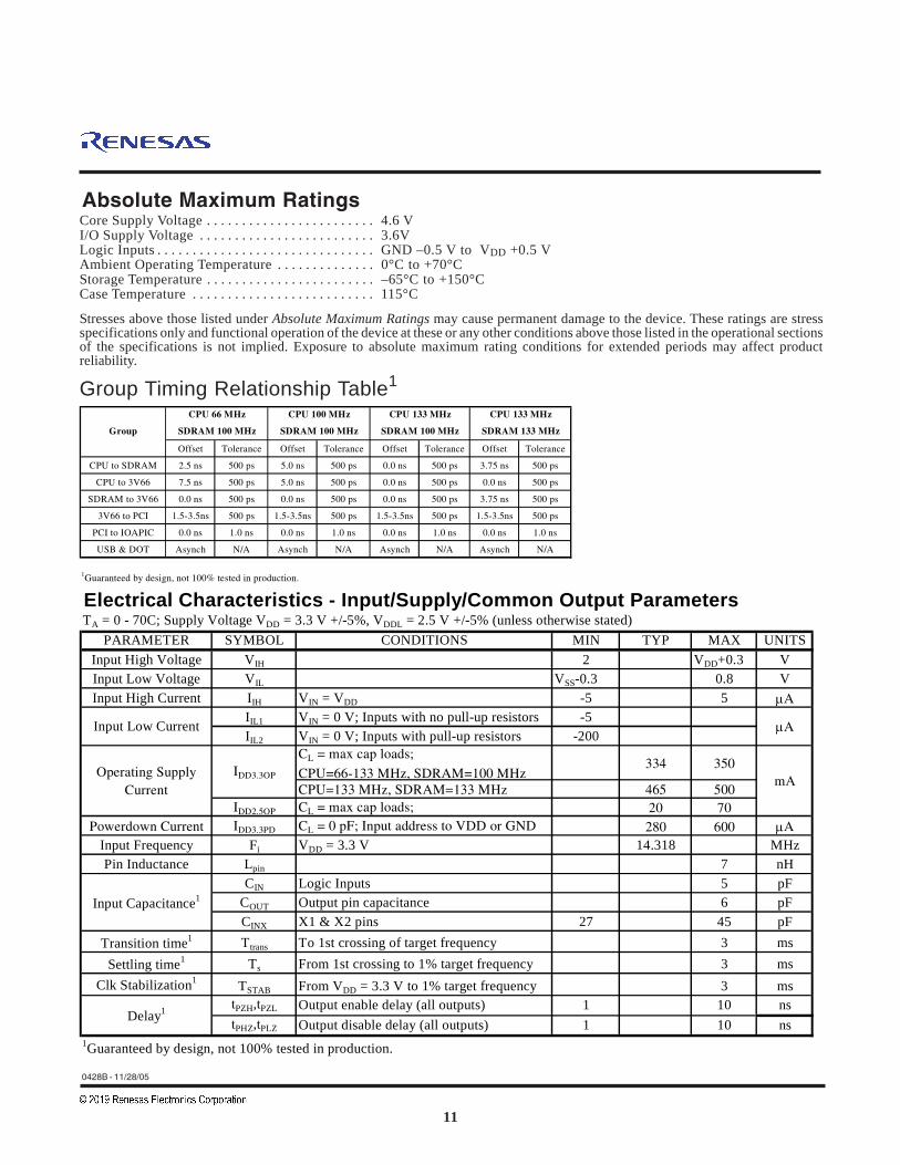
Absolute Maximum Ratings
Stresses above those listed under Absolute Maximum Ratings may cause permanent damage to the device. These ratings are stressspecifications only and functional operation of the device at these or any other conditions above those listed in the operational sectionsof the specifications is not implied. Exposure to absolute maximum rating conditions for extended periods may affect productreliability.
Core Supply Voltage . . . . . . . . . . . . . . . . . . . . . . . . 4.6 VI/O Supply Voltage . . . . . . . . . . . . . . . . . . . . . . . . . 3.6VLogic Inputs . . . . . . . . . . . . . . . . . . . . . . . . . . . . . . . GND –0.5 V to VDD +0.5 VAmbient Operating Temperature . . . . . . . . . . . . . . 0°C to +70°CStorage Temperature . . . . . . . . . . . . . . . . . . . . . . . . –65°C to +150°CCase Temperature . . . . . . . . . . . . . . . . . . . . . . . . . . 115°C
Group Timing Relationship Table1
Electrical Characteristics - Input/Supply/Common Output ParametersTA = 0 - 70C; Supply Voltage VDD = 3.3 V +/-5%, VDDL = 2.5 V +/-5% (unless otherwise stated)
PARAMETER SYMBOL CONDITIONS MIN TYP MAX UNITSInput High Voltage VIH 2 VDD+0.3 VInput Low Voltage VIL VSS-0.3 0.8 VInput High Current IIH VIN = VDD -5 5 µA
IIL1 VIN = 0 V; Inputs with no pull-up resistors -5IIL2 VIN = 0 V; Inputs with pull-up resistors -200
CL = max cap loads;
CPU=66-133 MHz, SDRAM=100 MHz334 350
CPU=133 MHz, SDRAM=133 MHz 465 500IDD2.5OP CL = max cap loads; 20 70
Powerdown Current IDD3.3PD CL = 0 pF; Input address to VDD or GND 280 600 µAInput Frequency Fi VDD = 3.3 V 14.318 MHzPin Inductance Lpin 7 nH
CIN Logic Inputs 5 pFCOUT Output pin capacitance 6 pFCINX X1 & X2 pins 27 45 pF
Transition time1 Ttrans To 1st crossing of target frequency 3 msSettling time1 Ts From 1st crossing to 1% target frequency 3 ms
Clk Stabilization1 TSTAB From VDD = 3.3 V to 1% target frequency 3 mstPZH,tPZL Output enable delay (all outputs) 1 10 nstPHZ,tPLZ Output disable delay (all outputs) 1 10 ns
1Guaranteed by design, not 100% tested in production.
Delay1
Input Capacitance1
Input Low Current µA
IDD3.3OPOperating Supply Current
mA
Offset Tolerance Offset Tolerance Offset Tolerance Offset Tolerance
CPU to SDRAM 2.5 ns 500 ps 5.0 ns 500 ps 0.0 ns 500 ps 3.75 ns 500 ps
CPU to 3V66 7.5 ns 500 ps 5.0 ns 500 ps 0.0 ns 500 ps 0.0 ns 500 ps
SDRAM to 3V66 0.0 ns 500 ps 0.0 ns 500 ps 0.0 ns 500 ps 3.75 ns 500 ps
3V66 to PCI 1.5-3.5ns 500 ps 1.5-3.5ns 500 ps 1.5-3.5ns 500 ps 1.5-3.5ns 500 ps
PCI to IOAPIC 0.0 ns 1.0 ns 0.0 ns 1.0 ns 0.0 ns 1.0 ns 0.0 ns 1.0 ns
USB & DOT Asynch N/A Asynch N/A Asynch N/A Asynch N/A
1Guaranteed by design, not 100% tested in production.
Group SDRAM 100 MHz SDRAM 100 MHz SDRAM 100 MHz SDRAM 133 MHz
CPU 66 MHz CPU 100 MHz CPU 133 MHz CPU 133 MHz
12
ICS94201
0428B - 11/28/05
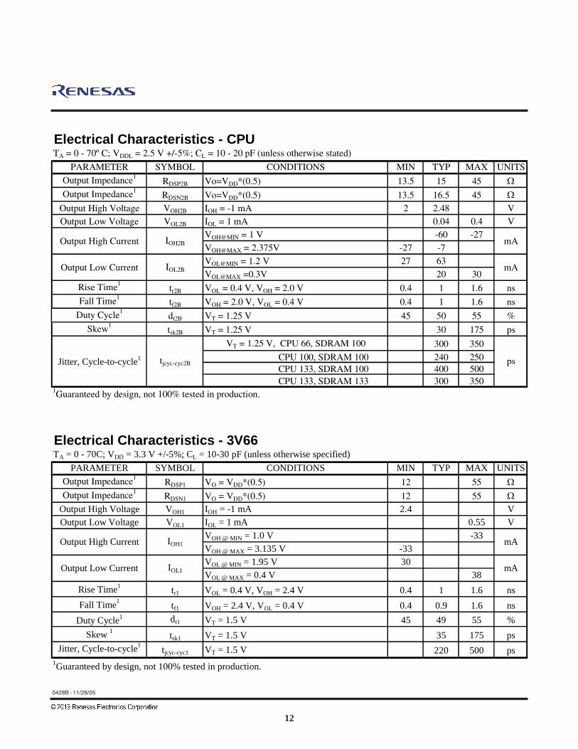
Electrical Characteristics - CPUTA = 0 - 70º C; VDDL = 2.5 V +/-5%; CL = 10 - 20 pF (unless otherwise stated)
PARAMETER SYMBOL CONDITIONS MIN TYP MAX UNITS
Output Impedance1RDSP2B Vo=VDD*(0.5) 13.5 15 45 Ω
Output Impedance1RDSN2B Vo=VDD*(0.5) 13.5 16.5 45 Ω
Output High Voltage VOH2B IOH = -1 mA 2 2.48 VOutput Low Voltage VOL2B IOL = 1 mA 0.04 0.4 V
VOH@MIN = 1 V -60 -27VOH@MAX = 2.375V -27 -7
VOL@MIN = 1.2 V 27 63VOL@MAX =0.3V 20 30
Rise Time1tr2B VOL = 0.4 V, VOH = 2.0 V 0.4 1 1.6 ns
Fall Time1tf2B VOH = 2.0 V, VOL = 0.4 V 0.4 1 1.6 ns
Duty Cycle1dt2B VT = 1.25 V 45 50 55 %
Skew1tsk2B VT = 1.25 V 30 175 ps
VT = 1.25 V, CPU 66, SDRAM 100 300 350
CPU 100, SDRAM 100 240 250 CPU 133, SDRAM 100 400 500 CPU 133, SDRAM 133 300 350
1Guaranteed by design, not 100% tested in production.
Jitter, Cycle-to-cycle1 tjcyc-cyc2B ps
mA
mA
Output High Current IOH2B
Output Low Current IOL2B
Electrical Characteristics - 3V66TA = 0 - 70C; VDD = 3.3 V +/-5%; CL = 10-30 pF (unless otherwise specified)
PARAMETER SYMBOL CONDITIONS MIN TYP MAX UNITSOutput Impedance1
RDSP1 VO = VDD*(0.5) 12 55 ΩOutput Impedance1
RDSN1 VO = VDD*(0.5) 12 55 ΩOutput High Voltage VOH1 IOH = -1 mA 2.4 VOutput Low Voltage VOL1 IOL = 1 mA 0.55 V
VOH @ MIN = 1.0 V -33VOH @ MAX = 3.135 V -33VOL @ MIN = 1.95 V 30VOL @ MAX = 0.4 V 38
Rise Time1 tr1 VOL = 0.4 V, VOH = 2.4 V 0.4 1 1.6 nsFall Time1 tf1 VOH = 2.4 V, VOL = 0.4 V 0.4 0.9 1.6 ns
Duty Cycle1 dt1 VT = 1.5 V 45 49 55 %Skew 1 tsk1 VT = 1.5 V 35 175 ps
Jitter, Cycle-to-cycle1 tjcyc-cyc1 VT = 1.5 V 220 500 ps1Guaranteed by design, not 100% tested in production.
Output High Current
Output Low Current
mA
mA
IOH1
IOL1
13
ICS94201
0428B - 11/28/05
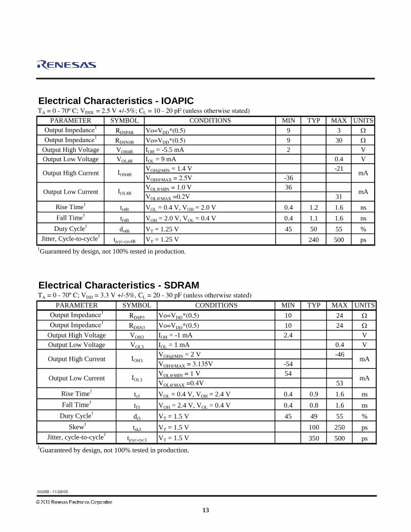
Electrical Characteristics - IOAPICTA = 0 - 70º C; VDDL = 2.5 V +/-5%; CL = 10 - 20 pF (unless otherwise stated)
PARAMETER SYMBOL CONDITIONS MIN TYP MAX UNITSOutput Impedance1
RDSP4B Vo=VDD*(0.5) 9 3 ΩOutput Impedance1
RDSN4B Vo=VDD*(0.5) 9 30 ΩOutput High Voltage VOH4B IOH = -5.5 mA 2 VOutput Low Voltage VOL4B IOL = 9 mA 0.4 V
VOH@MIN = 1.4 V -21VOH@MAX = 2.5V -36VOL@MIN = 1.0 V 36VOL@MAX =0.2V 31
Rise Time1 tr4B VOL = 0.4 V, VOH = 2.0 V 0.4 1.2 1.6 nsFall Time1 tf4B VOH = 2.0 V, VOL = 0.4 V 0.4 1.1 1.6 ns
Duty Cycle1 dt4B VT = 1.25 V 45 50 55 %Jitter, Cycle-to-cycle1
tjcyc-cyc4B VT = 1.25 V 240 500 ps1Guaranteed by design, not 100% tested in production.
mA
mA
Output High Current IOH4B
Output Low Current IOL4B
Electrical Characteristics - SDRAMTA = 0 - 70º C; VDD = 3.3 V +/-5%, CL = 20 - 30 pF (unless otherwise stated)
PARAMETER SYMBOL CONDITIONS MIN TYP MAX UNITSOutput Impedance1
RDSP3 Vo=VDD*(0.5) 10 24 ΩOutput Impedance1
RDSN3 Vo=VDD*(0.5) 10 24 ΩOutput High Voltage VOH3 IOH = -1 mA 2.4 VOutput Low Voltage VOL3 IOL = 1 mA 0.4 V
VOH@MIN = 2 V -46VOH@MAX = 3.135V -54VOL@MIN = 1 V 54VOL@MAX =0.4V 53
Rise Time1 tr3 VOL = 0.4 V, VOH = 2.4 V 0.4 0.9 1.6 nsFall Time1 tf3 VOH = 2.4 V, VOL = 0.4 V 0.4 0.8 1.6 ns
Duty Cycle1 dt3 VT = 1.5 V 45 49 55 % Skew1 tsk3 VT = 1.5 V 100 250 ps
Jitter, cycle-to-cycle1 tjcyc-cyc3 VT = 1.5 V 350 500 ps1Guaranteed by design, not 100% tested in production.
mA
mA
Output High Current IOH3
Output Low Current IOL3
14
ICS94201
0428B - 11/28/05
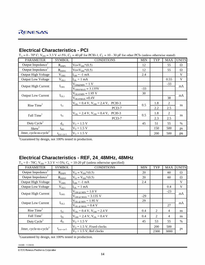
Electrical Characteristics - PCITA = 0 - 70º C; VDD = 3.3 V +/-5%, CL = 40 pF for PCI0-1, CL = 10 - 30 pF for other PCIs (unless otherwise stated)
PARAMETER SYMBOL CONDITIONS MIN TYP MAX UNITSOutput Impedance1
RDSP1 Vo=VDD*(0.5) 12 55 ΩOutput Impedance1
RDSN1 Vo=VDD*(0.5) 12 55 ΩOutput High Voltage VOH1 IOH = -1 mA 2.4 VOutput Low Voltage VOL1 IOL = 1 mA 0.55 V
VOH@MIN = 1 V -33VOH@MAX = 3.135V -33VOL@MIN = 1.95 V 30VOL@MAX =0.4V 38VOL = 0.4 V, VOH = 2.4 V, PCI0-3 1.8 2
PCI3-7 2.2 2.5VOL = 2.4 V, VOH = 0.4 V, PCI0-3 1.8 2
PCI3-7 2.3 2.5Duty Cycle1 dt1 VT = 1.5 V 45 51 55 %
Skew1 tsk1 VT = 1.5 V 150 500 psJitter, cycle-to-cycle1 tjcyc-cyc1 VT = 1.5 V 200 500 ps
1Guaranteed by design, not 100% tested in production.
mA
mA
Output High Current IOH1
Output Low Current IOL1
tr1Rise Time1
Fall Time1 tf1
ns
ns0.5
0.5
Electrical Characteristics - REF, 24_48MHz, 48MHzTA = 0 - 70C; VDD = 3.3 V +/-5%; CL = 10-20 pF (unless otherwise specified)
PARAMETER SYMBOL CONDITIONS MIN TYP MAX UNITSOutput Impedance1
RDSP5 VO = VDD*(0.5) 20 60 ΩOutput Impedance1
RDSN5 VO = VDD*(0.5) 20 60 ΩOutput High Voltage VOH5 IOH = -1 mA 2.4 VOutput Low Voltage VOL5 IOL = 1 mA 0.4 V
VOH @ MIN = 1.0 V -23VOH @ MAX = 3.135 V -29VOL @ MIN = 1.95 V 29VOL @ MAX = 0.4 V 27
Rise Time1 tr5 VOL = 0.4 V, VOH = 2.4 V 0.4 2 4 nsFall Time1 tf5 VOH = 2.4 V, VOL = 0.4 V 0.4 2 4 ns
Duty Cycle1 dt5 VT = 1.5 V 45 53 55 %VT = 1.5 V, Fixed clocks 200 500VT = 1.5 V, Ref clocks 2300 3000
1Guaranteed by design, not 100% tested in production.
Jitter, cycle-to-cycle1 tjcyc-cyc5 ps
Output High Current IOH5 mA
Output Low Current IOL5 mA
15
ICS94201
0428B - 11/28/05
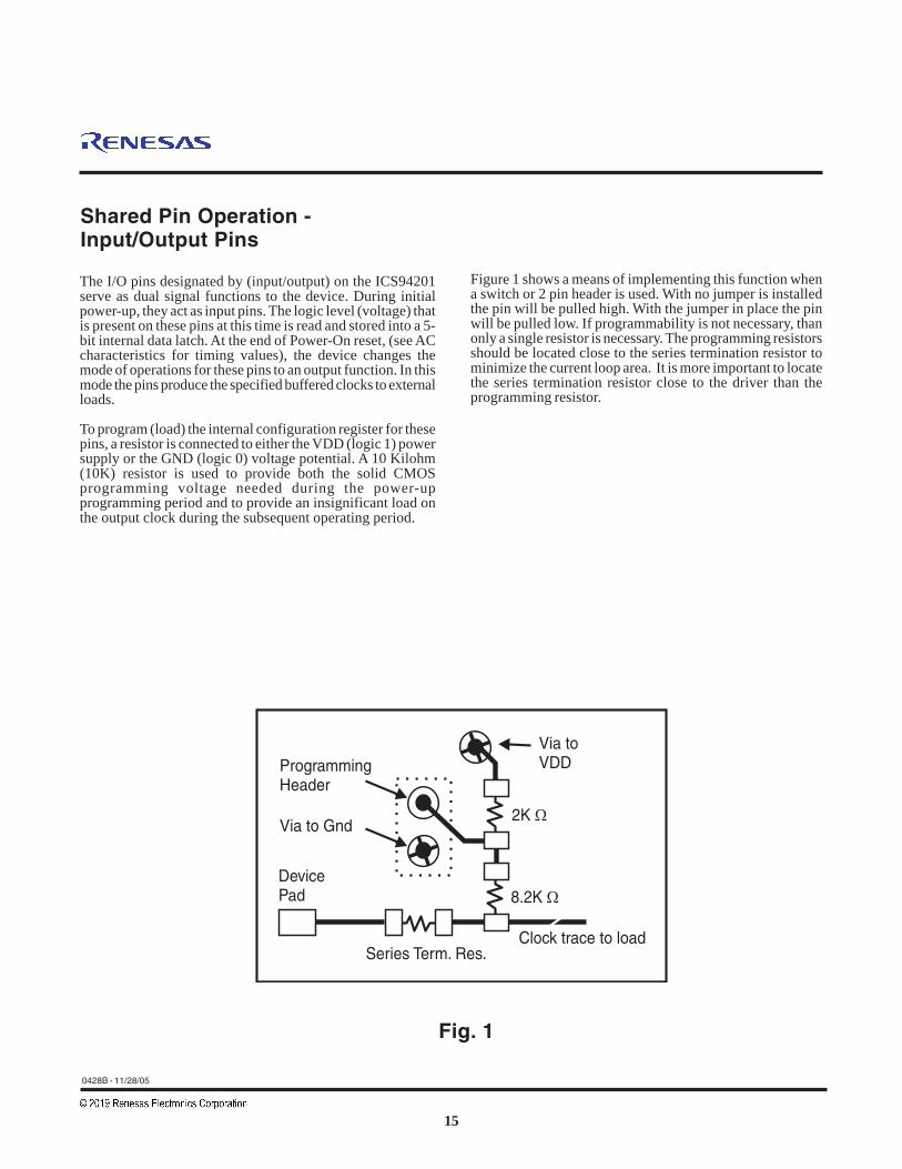
Fig. 1
Shared Pin Operation -Input/Output Pins
The I/O pins designated by (input/output) on the ICS94201serve as dual signal functions to the device. During initialpower-up, they act as input pins. The logic level (voltage) thatis present on these pins at this time is read and stored into a 5-bit internal data latch. At the end of Power-On reset, (see ACcharacteristics for timing values), the device changes themode of operations for these pins to an output function. In thismode the pins produce the specified buffered clocks to externalloads.
To program (load) the internal configuration register for thesepins, a resistor is connected to either the VDD (logic 1) powersupply or the GND (logic 0) voltage potential. A 10 Kilohm(10K) resistor is used to provide both the solid CMOSprogramming voltage needed during the power-upprogramming period and to provide an insignificant load onthe output clock during the subsequent operating period.
Via toVDD
Clock trace to loadSeries Term. Res.
ProgrammingHeader
Via to Gnd
DevicePad
2K
8.2K
Figure 1 shows a means of implementing this function whena switch or 2 pin header is used. With no jumper is installedthe pin will be pulled high. With the jumper in place the pinwill be pulled low. If programmability is not necessary, thanonly a single resistor is necessary. The programming resistorsshould be located close to the series termination resistor tominimize the current loop area. It is more important to locatethe series termination resistor close to the driver than theprogramming resistor.
16
ICS94201
0428B - 11/28/05
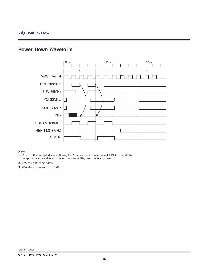
Power Down Waveform
Note1. After PD# is sampled active (Low) for 2 consective rising edges of CPUCLKs, all the
output clocks are driven Low on their next High to Low tranistiion.2. Power-up latency <3ms.3. Waveform shown for 100MHz
17
ICS94201
0428B - 11/28/05
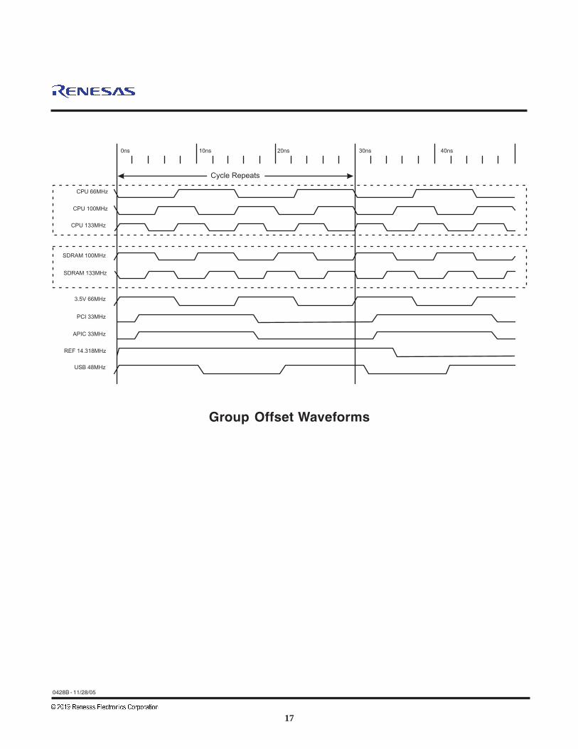
Group Offset Waveforms
Cycle Repeats
0ns
CPU 66MHz
CPU 100MHz
CPU 133MHz
SDRAM 133MHz
SDRAM 100MHz
3.5V 66MHz
PCI 33MHz
APIC 33MHz
REF 14.318MHz
USB 48MHz
10ns 20ns 30ns 40ns
18
ICS94201
0428B - 11/28/05
INDEX
AREA
INDEX
AREA
1 21 2
N
Dh x 45°h x 45°
E1 E
SEATING
PLANE
SEATING
PLANE
A1
A
e
- C -- C -
b
.10 (.004) C.10 (.004) C
c
L
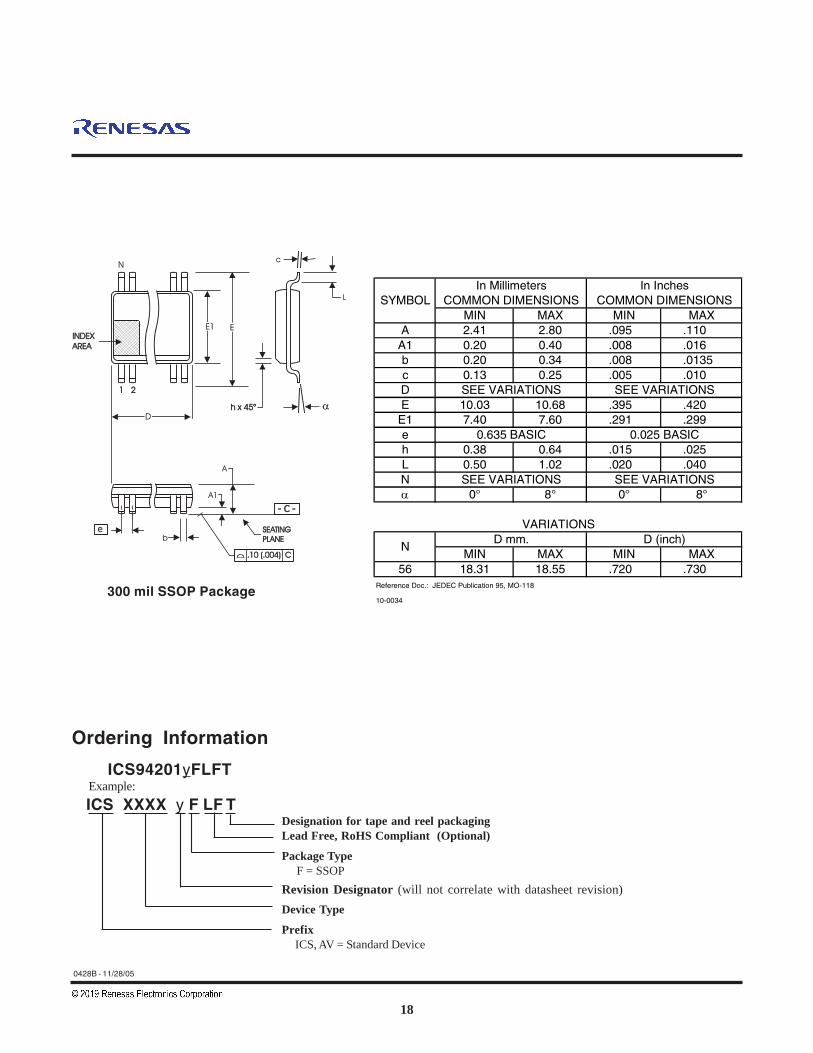
300 mil SSOP Package
MIN MAX MIN MAXA 2.41 2.80 .095 .110
A1 0.20 0.40 .008 .016b 0.20 0.34 .008 .0135c 0.13 0.25 .005 .010DE 10.03 10.68 .395 .420
E1 7.40 7.60 .291 .299eh 0.38 0.64 .015 .025L 0.50 1.02 .020 .040Nα 0° 8° 0° 8°
MIN MAX MIN MAX56 18.31 18.55 .720 .730
10-0034
SYMBOLIn Millimeters In Inches
COMMON DIMENSIONS COMMON DIMENSIONS
SEE VARIATIONS SEE VARIATIONS
0.635 BASIC 0.025 BASIC
Reference Doc.: JEDEC Publication 95, MO-118
VARIATIONS
SEE VARIATIONS SEE VARIATIONS
ND mm. D (inch)
Ordering Information
ICS94201yFLFTExample:
Designation for tape and reel packagingLead Free, RoHS Compliant (Optional)
Package Type F = SSOPRevision Designator (will not correlate with datasheet revision)Device Type
Prefix ICS, AV = Standard Device
ICS XXXX y F LF T

19
ICS94201
0428B - 11/28/05
Revision HistoryRev. Issue Date Description Page #
B 11/28/2005 Added LF Ordering Information 18
Corporate HeadquartersTOYOSU FORESIA, 3-2-24 Toyosu,Koto-ku, Tokyo 135-0061, Japanwww.renesas.com
Contact InformationFor further information on a product, technology, the most up-to-date version of a document, or your nearest sales office, please visit:www.renesas.com/contact/
TrademarksRenesas and the Renesas logo are trademarks of Renesas Electronics Corporation. All trademarks and registered trademarks are the property of their respective owners.
IMPORTANT NOTICE AND DISCLAIMER
RENESAS ELECTRONICS CORPORATION AND ITS SUBSIDIARIES (“RENESAS”) PROVIDES TECHNICAL SPECIFICATIONS AND RELIABILITY DATA (INCLUDING DATASHEETS), DESIGN RESOURCES (INCLUDING REFERENCE DESIGNS), APPLICATION OR OTHER DESIGN ADVICE, WEB TOOLS, SAFETY INFORMATION, AND OTHER RESOURCES “AS IS” AND WITH ALL FAULTS, AND DISCLAIMS ALL WARRANTIES, EXPRESS OR IMPLIED, INCLUDING, WITHOUT LIMITATION, ANY IMPLIED WARRANTIES OF MERCHANTABILITY, FITNESS FOR A PARTICULAR PURPOSE, OR NON-INFRINGEMENT OF THIRD PARTY INTELLECTUAL PROPERTY RIGHTS.
These resources are intended for developers skilled in the art designing with Renesas products. You are solely responsible for (1) selecting the appropriate products for your application, (2) designing, validating, and testing your application, and (3) ensuring your application meets applicable standards, and any other safety, security, or other requirements. These resources are subject to change without notice. Renesas grants you permission to use these resources only for development of an application that uses Renesas products. Other reproduction or use of these resources is strictly prohibited. No license is granted to any other Renesas intellectual property or to any third party intellectual property. Renesas disclaims responsibility for, and you will fully indemnify Renesas and its representatives against, any claims, damages, costs, losses, or liabilities arising out of your use of these resources. Renesas' products are provided only subject to Renesas' Terms and Conditions of Sale or other applicable terms agreed to in writing. No use of any Renesas resources expands or otherwise alters any applicable warranties or warranty disclaimers for these products.
(Rev.1.0 Mar 2020)
© 2020 Renesas Electronics Corporation. All rights reserved.