Embed Size (px)
Citation preview
FLAT-16 SMD5C:5-connection SMD
Features• Operating input voltage from 3 V to 12 V• Adjustable output voltage• 3 A maximum guaranteed output current in SMD5C package, 2 A in FLAT-16• Very low dropout voltage: 350 mV typ. @ 400 mA• Embedded overtemperature and overcurrent protection• Adjustable overcurrent limitation• Very low noise: 40 µVRMS (10 Hz-100 kHz)• Output overload monitoring/signalling• Inhibit (ON/OFF) TTL-compatible control• Programmable output short-circuit current• Remote sensing operation• Low quiescent current: 1.5 mA typ. @ no load, 150 µA in shutdown• Rad-hard: guaranteed up to 300 krad Mil Std 883E Method 1019.6 high dose
rate and 0.01 rad/s in ELDRS conditions• Heavy ion, SEL immune.
DescriptionThe RHFL4913A is a high-performance adjustable positive voltage regulator, able toprovide 2 A of maximum current in FLAT-16 package (3 A in the SMD5C package)from an input voltage ranging from 3 V to 12 V, with a typical dropout voltage of 350mV.
The RHFL4913A features exceptional radiation performances. It is tested inaccordance with Mil Std 883E Method 1019.6, in ELDRS conditions. The device isavailable in the FLAT-16 and the SMD5C hermetic ceramic package, and the QML-Vdie is specifically designed for space and harsh radiation environments. It operateswith an input supply of up to 12 V. The RHFL4913A is QML-V qualified, DSCC SMD#5962F02524.
Maturity status link
RHFL4913A
Rad-hard adjustable positive voltage regulator
RHFL4913A
Datasheet
DS3625 - Rev 20 - April 2018For further information contact your local STMicroelectronics sales office.
www.st.com

1 Diagram
Figure 1. Block diagram
AMG081120161300MT
RHFL4913ADiagram
DS3625 - Rev 20 page 2/31

2 Pin configuration
Figure 2. Pin configuration (top view for FLAT-16, bottom view for SMD5C)
FLAT-16 SMD5CAMG081120161301MT
Table 1. Pin description
Pin name FLAT-16 (1) SMD5C (2)
VO 1, 2, 6, 7 1
VI 3, 4, 5 4
GND 13 5
ISC 8
OCM 10
INHIBIT 14 3
ADJ 15 2
NC 9, 11, 12, 16
1. The upper metallic package lid and the bottom metallization are neither connected to regulator die nor topackage terminals, hence electrically floating.
2. The upper metallic package lid is neither connected to regulator die nor to package terminals, henceelectrically floating.
RHFL4913APin configuration
DS3625 - Rev 20 page 3/31
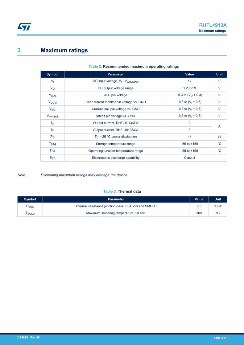
3 Maximum ratings
Table 2. Recommended maximum operating ratings
Symbol Parameter Value Unit
VI DC input voltage, VI - VGROUND 12 V
VO DC output voltage range 1.23 to 9 V
VADJ ADJ pin voltage -0.3 to (VO + 0.3) V
VOCM Over current monitor pin voltage vs. GND -0.3 to (VI + 0.3) V
VISC Current limit pin voltage vs. GND -0.3 to (VI + 0.3) V
VINHIBIT Inhibit pin voltage vs. GND -0.3 to (VI + 0.3) V
IO Output current, RHFL4913KPA 2A
IO Output current, RHFL4913SCA 3
PD TC = 25 °C power dissipation 15 W
TSTG Storage temperature range -65 to +150 °C
TOP Operating junction temperature range -55 to +150 °C
ESD Electrostatic discharge capability Class 3
Note: Exceeding maximum ratings may damage the device.
Table 3. Thermal data
Symbol Parameter Value Unit
RthJC Thermal resistance junction-case, FLAT-16 and SMD5C 8.3 °C/W
TSOLD Maximum soldering temperature, 10 sec. 300 °C
RHFL4913AMaximum ratings
DS3625 - Rev 20 page 4/31
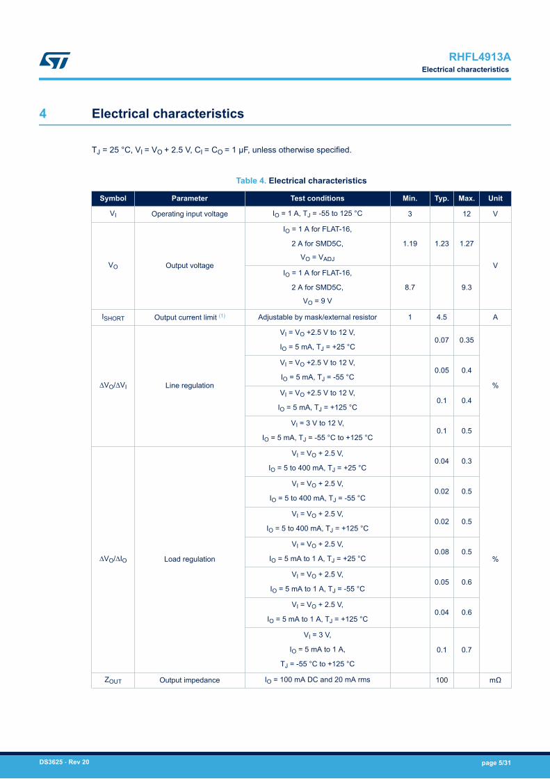
4 Electrical characteristics
TJ = 25 °C, VI = VO + 2.5 V, CI = CO = 1 µF, unless otherwise specified.
Table 4. Electrical characteristics
Symbol Parameter Test conditions Min. Typ. Max. Unit
VI Operating input voltage IO = 1 A, TJ = -55 to 125 °C 3 12 V
VO Output voltage
IO = 1 A for FLAT-16,
2 A for SMD5C,
VO = VADJ
1.19 1.23 1.27
VIO = 1 A for FLAT-16,
2 A for SMD5C,
VO = 9 V
8.7 9.3
ISHORT Output current limit (1) Adjustable by mask/external resistor 1 4.5 A
∆VO/∆VI Line regulation
VI = VO +2.5 V to 12 V,
IO = 5 mA, TJ = +25 °C0.07 0.35
%
VI = VO +2.5 V to 12 V,
IO = 5 mA, TJ = -55 °C0.05 0.4
VI = VO +2.5 V to 12 V,
IO = 5 mA, TJ = +125 °C0.1 0.4
VI = 3 V to 12 V,
IO = 5 mA, TJ = -55 °C to +125 °C0.1 0.5
∆VO/∆IO Load regulation
VI = VO + 2.5 V,
IO = 5 to 400 mA, TJ = +25 °C0.04 0.3
%
VI = VO + 2.5 V,
IO = 5 to 400 mA, TJ = -55 °C0.02 0.5
VI = VO + 2.5 V,
IO = 5 to 400 mA, TJ = +125 °C0.02 0.5
VI = VO + 2.5 V,
IO = 5 mA to 1 A, TJ = +25 °C0.08 0.5
VI = VO + 2.5 V,
IO = 5 mA to 1 A, TJ = -55 °C0.05 0.6
VI = VO + 2.5 V,
IO = 5 mA to 1 A, TJ = +125 °C0.04 0.6
VI = 3 V,
IO = 5 mA to 1 A,
TJ = -55 °C to +125 °C
0.1 0.7
ZOUT Output impedance IO = 100 mA DC and 20 mA rms 100 mΩ
RHFL4913AElectrical characteristics
DS3625 - Rev 20 page 5/31
Symbol Parameter Test conditions Min. Typ. Max. Unit
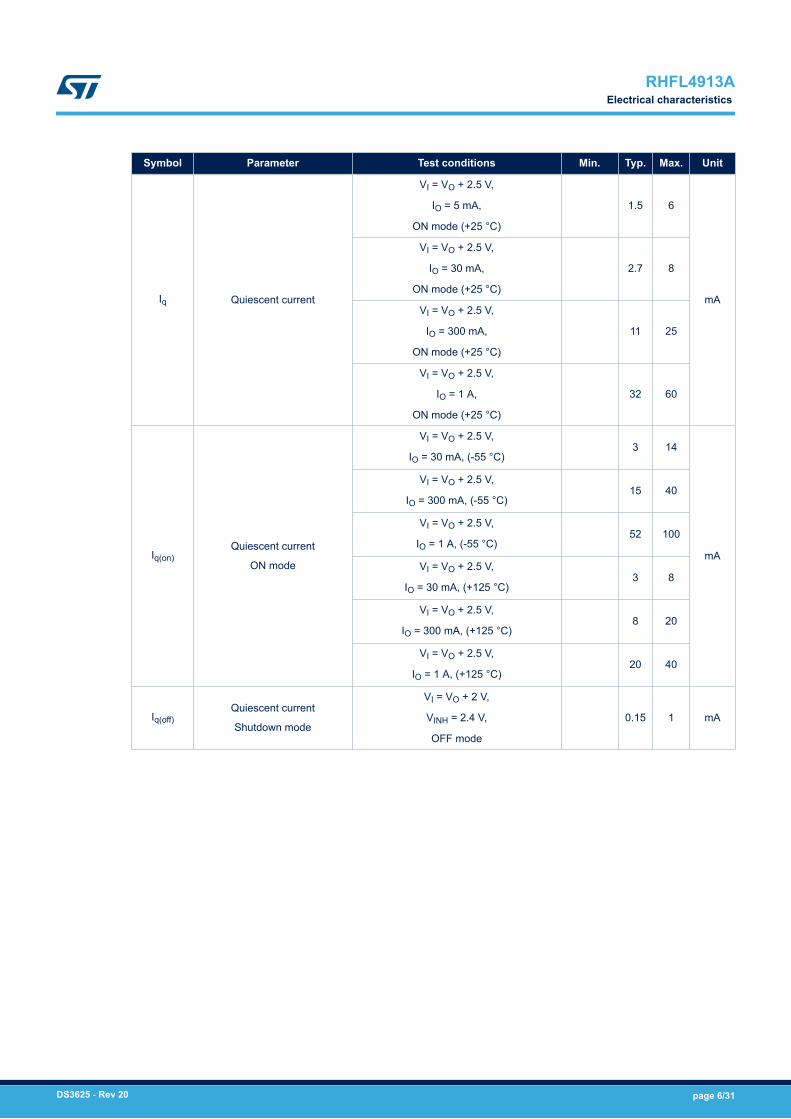
Iq Quiescent current
VI = VO + 2.5 V,
IO = 5 mA,
ON mode (+25 °C)
1.5 6
mA
VI = VO + 2.5 V,
IO = 30 mA,
ON mode (+25 °C)
2.7 8
VI = VO + 2.5 V,
IO = 300 mA,
ON mode (+25 °C)
11 25
VI = VO + 2.5 V,
IO = 1 A,
ON mode (+25 °C)
32 60
Iq(on)Quiescent current
ON mode
VI = VO + 2.5 V,
IO = 30 mA, (-55 °C)3 14
mA
VI = VO + 2.5 V,
IO = 300 mA, (-55 °C)15 40
VI = VO + 2.5 V,
IO = 1 A, (-55 °C)52 100
VI = VO + 2.5 V,
IO = 30 mA, (+125 °C)3 8
VI = VO + 2.5 V,
IO = 300 mA, (+125 °C)8 20
VI = VO + 2.5 V,
IO = 1 A, (+125 °C)20 40
Iq(off)Quiescent current
Shutdown mode
VI = VO + 2 V,
VINH = 2.4 V,
OFF mode
0.15 1 mA
RHFL4913AElectrical characteristics
DS3625 - Rev 20 page 6/31

Symbol Parameter Test conditions Min. Typ. Max. Unit
Vd Dropout voltage
IO = 0 mA, VO = 2.5 V to 9 V 130
mV
IO = 400 mA,
VO = 2.5 to 9 V, (+25 °C)350 450
IO = 400 mA,
VO = 2.5 to 9 V, (-55 °C)300 400
IO = 400 mA,
VO = 2.5 to 9 V, (+125 °C)450 550
IO = 1 A,
VO = 2.5 to 9 V, (+25 °C)500 650
IO = 1 A,
VO = 2.5 to 9 V, (-55 °C)400 550
IO = 1 A,
VO = 2.5 to 9 V, (+125 °C)640 800
IO = 2 A,
VO = 2.5 to 9 V, (+25 °C)750
IO = 2 A,
VO = 2.5 to 9 V, (+125 °C)950
VINH(ON) Inhibit voltage IO = 5 mA, TJ = -55 to +125 °C 0.8V
VINH(OFF) Inhibit voltage IO = 5 mA, TJ = -55 to +125 °C 2.4
SVR Supply voltage rejection (1)
VI = VO + 2.5 V ± 0.5 V,
VO = 3 V, IO = 5 mA
f = 120 Hz
60 70
dBVI = VO + 2.5 V ± 0.5 V,
VO = 3 V, IO = 5 mA
f = 33 kHz
30 40
ISH Shutdown input current VINH = 5 V 15 µA
VOCM OCM pin voltage Sinked IOCM = 24 mA active low 0.38 V
tPLH
tPHLInhibit propagation delay (1)
VI = VO + 2.5 V,
VINH = 2.4 V,
IO = 400 mA,
VO = 3 V
ON-OFF 20 µs
OFF-ON 100 µs
eN Output noise voltage (1)B = 10 Hz to 100 kHz,
IO = 5 mA to 2 A40 µVrms
1. These values are guaranteed by design. For each application it is strongly recommended to comply with the maximumcurrent limit of the package used.
RHFL4913AElectrical characteristics
DS3625 - Rev 20 page 7/31

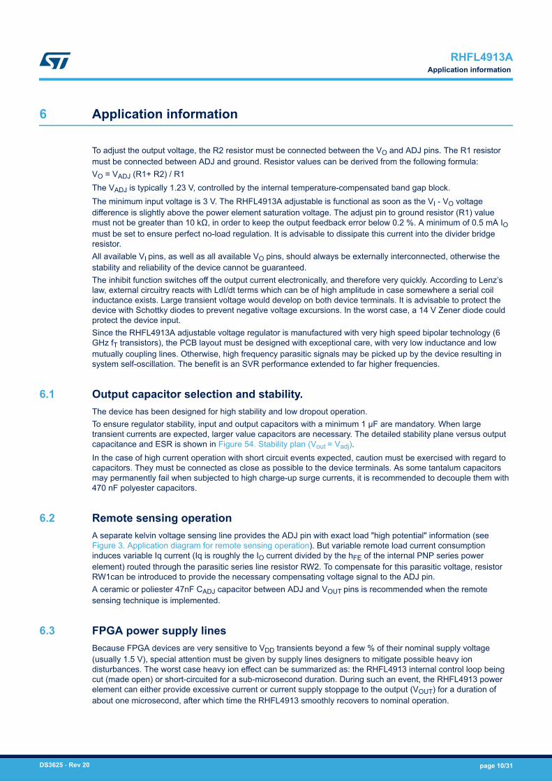
Figure 3. Application diagram for remote sensing operation
InputSupply
DUT
REMOTE
SENSE
CI
RW1 RW2
R1
R2
Co
VI
Vo1Vo2
GNDADJ
CADJ(47 nF)
AMG081120161302MT
RHFL4913AElectrical characteristics
DS3625 - Rev 20 page 8/31

5 Device description
The RHFL4913A adjustable voltage regulator contains a PNP type power element controlled by a signal resultingfrom an amplified comparison between the internal temperature-compensated band-gap and the fraction of thedesired output voltage value obtained from an external resistor divider bridge. The device is protected by severalfunctional blocks.
5.1 ADJ pinThe load output voltage feedback comes from an external resistor divider bridge mid-point connected to the ADJpin (allowing all possible output voltage settings as per user requirements) established between load terminals.
5.2 Inhibit ON-OFF controlBy setting the INHIBIT pin TTL high, the device switches off the output current and voltage. The device is ONwhen the INHIBIT pin is set low. Since the INHIBIT pin is pulled down internally, it can be left floating in caseswhere the inhibit function is not used.
5.3 Overtemperature protectionA temperature detector internally monitors the power element junction temperature. The device turns off when atemperature of approximately 175 °C is reached, returning to ON mode when back to approximately 135 °C.Combined with the other protection blocks, the device is protected from destructive junction temperatureexcursions in all load conditions. It should be noted that when the internal temperature detector reaches 175 °C,the active power element can be as high as 225 °C. Prolonged operation under these conditions far exceeds themaximum operating ratings and device reliability cannot be guaranteed.
5.4 Programmable overcurrent protectionAn internal non fold-back short circuit limitation is set with ISHORT > 3.8 A (VO is 0 V). This value can bedecreased via an external RSH resistor connected between the ISC and VI pins, with a typical value range of 10kΩ to 200 kΩ (refer to Figure 44. Short circuit current vs. RSH and Figure 45. Short circuit current vs. RSH(zoom)).To maintain optimal VO regulation, it is necessary to set ISHORT 1.6 times greater than the maximumdesired application IO. When IO reaches ISHORT – 300 mA, the current limiter overrules the regulation, VO starts todrop and the OCM flag is raised. When no current limitation adjustment is required, the ISC pin must be leftunbiased (as it is in 3 pin packages).
5.5 OCM pinThe OCM pin goes low when the current limit becomes active, otherwise VOCM = VI. It is buffered and can sink 10mA. The OCM pin is internally pulled up by a 5 kΩ resistor.
RHFL4913ADevice description
DS3625 - Rev 20 page 9/31
6 Application information
To adjust the output voltage, the R2 resistor must be connected between the VO and ADJ pins. The R1 resistormust be connected between ADJ and ground. Resistor values can be derived from the following formula:VO = VADJ (R1+ R2) / R1The VADJ is typically 1.23 V, controlled by the internal temperature-compensated band gap block.The minimum input voltage is 3 V. The RHFL4913A adjustable is functional as soon as the VI - VO voltagedifference is slightly above the power element saturation voltage. The adjust pin to ground resistor (R1) valuemust not be greater than 10 kΩ, in order to keep the output feedback error below 0.2 %. A minimum of 0.5 mA IOmust be set to ensure perfect no-load regulation. It is advisable to dissipate this current into the divider bridgeresistor.All available VI pins, as well as all available VO pins, should always be externally interconnected, otherwise thestability and reliability of the device cannot be guaranteed.The inhibit function switches off the output current electronically, and therefore very quickly. According to Lenz’slaw, external circuitry reacts with LdI/dt terms which can be of high amplitude in case somewhere a serial coilinductance exists. Large transient voltage would develop on both device terminals. It is advisable to protect thedevice with Schottky diodes to prevent negative voltage excursions. In the worst case, a 14 V Zener diode couldprotect the device input.Since the RHFL4913A adjustable voltage regulator is manufactured with very high speed bipolar technology (6GHz fT transistors), the PCB layout must be designed with exceptional care, with very low inductance and lowmutually coupling lines. Otherwise, high frequency parasitic signals may be picked up by the device resulting insystem self-oscillation. The benefit is an SVR performance extended to far higher frequencies.
6.1 Output capacitor selection and stability.The device has been designed for high stability and low dropout operation.To ensure regulator stability, input and output capacitors with a minimum 1 µF are mandatory. When largetransient currents are expected, larger value capacitors are necessary. The detailed stability plane versus outputcapacitance and ESR is shown in Figure 54. Stability plan (Vout = Vadj).In the case of high current operation with short circuit events expected, caution must be exercised with regard tocapacitors. They must be connected as close as possible to the device terminals. As some tantalum capacitorsmay permanently fail when subjected to high charge-up surge currents, it is recommended to decouple them with470 nF polyester capacitors.
6.2 Remote sensing operationA separate kelvin voltage sensing line provides the ADJ pin with exact load "high potential" information (seeFigure 3. Application diagram for remote sensing operation). But variable remote load current consumptioninduces variable Iq current (Iq is roughly the IO current divided by the hFE of the internal PNP series powerelement) routed through the parasitic series line resistor RW2. To compensate for this parasitic voltage, resistorRW1can be introduced to provide the necessary compensating voltage signal to the ADJ pin.A ceramic or poliester 47nF CADJ capacitor between ADJ and VOUT pins is recommended when the remotesensing technique is implemented.
6.3 FPGA power supply linesBecause FPGA devices are very sensitive to VDD transients beyond a few % of their nominal supply voltage(usually 1.5 V), special attention must be given by supply lines designers to mitigate possible heavy iondisturbances. The worst case heavy ion effect can be summarized as: the RHFL4913 internal control loop beingcut (made open) or short-circuited for a sub-microsecond duration. During such an event, the RHFL4913 powerelement can either provide excessive current or current supply stoppage to the output (VOUT) for a duration ofabout one microsecond, after which time the RHFL4913 smoothly recovers to nominal operation.
RHFL4913AApplication information
DS3625 - Rev 20 page 10/31
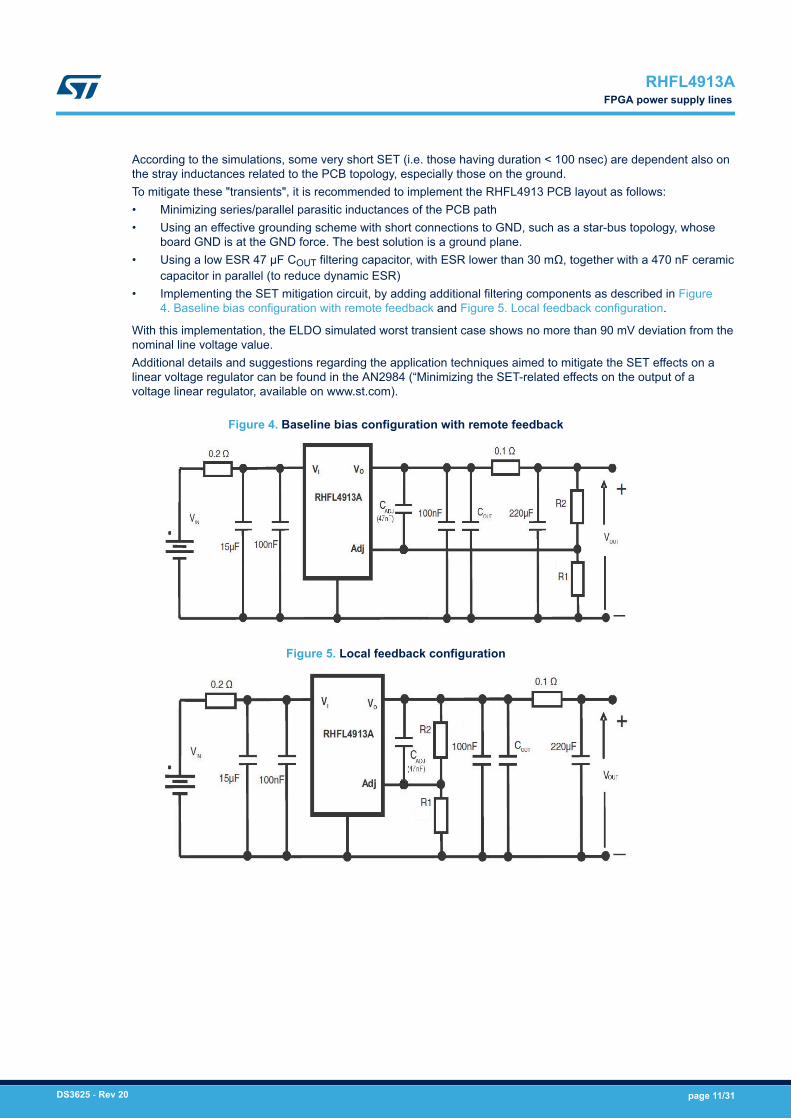
According to the simulations, some very short SET (i.e. those having duration < 100 nsec) are dependent also onthe stray inductances related to the PCB topology, especially those on the ground.To mitigate these "transients", it is recommended to implement the RHFL4913 PCB layout as follows:• Minimizing series/parallel parasitic inductances of the PCB path• Using an effective grounding scheme with short connections to GND, such as a star-bus topology, whose
board GND is at the GND force. The best solution is a ground plane.• Using a low ESR 47 µF COUT filtering capacitor, with ESR lower than 30 mΩ, together with a 470 nF ceramic
capacitor in parallel (to reduce dynamic ESR)• Implementing the SET mitigation circuit, by adding additional filtering components as described in Figure
4. Baseline bias configuration with remote feedback and Figure 5. Local feedback configuration.
With this implementation, the ELDO simulated worst transient case shows no more than 90 mV deviation from thenominal line voltage value.Additional details and suggestions regarding the application techniques aimed to mitigate the SET effects on alinear voltage regulator can be found in the AN2984 (“Minimizing the SET-related effects on the output of avoltage linear regulator, available on www.st.com).
Figure 4. Baseline bias configuration with remote feedback
Figure 5. Local feedback configuration
RHFL4913AFPGA power supply lines
DS3625 - Rev 20 page 11/31
6.4 Notes on the 16-pin hermetic packageThe bottom section of the 16-pin package is metallized in order to allow the user to directly solder theRHFL4913A onto PCB, no heat sink needed for enhanced heat removal.This AlN ceramic package features a low thermal coefficient of expansion (TCE) significantly lower than the TCEof some PCBs. It is therefore recommended, especially when its bottom metallic dissipation plate is brazed (asopposed to glued), to carefully design the PCB (material, thickness, layout…) and the mounting process to securethat the package and the solder joint can sustain the worst case temperature cycling its must be qualified for(highest constraints are at lowest temperature). It is strongly recommended to make sure that the actual mountingis well covered by the qualified mounting process for each parameters (PCB material, thickness, layout,temperature profile...).
RHFL4913ANotes on the 16-pin hermetic package
DS3625 - Rev 20 page 12/31
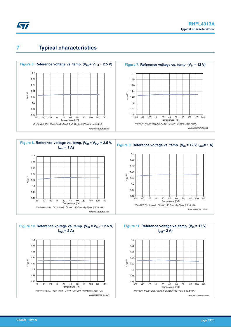
7 Typical characteristics
Figure 6. Reference voltage vs. temp. (Vin = Vout + 2.5 V)
1.16
1.18
1.2
1.22
1.24
1.26
1.28
1.3
-60 -40 -20 0 20 40 60 80 100 120 140
VR
EF [V
]
Temperature [ °C]
Vin=Vout+2.5V, Vout =Vadj , Cin=0.1 μF, Cout =1μF(tant ), Iout =5mA
AMG081120161305MT
Figure 7. Reference voltage vs. temp. (Vin = 12 V)
Vin=12V, Vout =Vadj , Cin=0.1 μF, Cout =1μF(tant ), Iout =5mA
1.16
1.18
1.2
1.22
1.24
1.26
1.28
1.3
-60 -40 -20 0 20 40 60 80 100 120 140
VR
EF [V
]
Temperature [ °C]
AMG081120161306MT
Figure 8. Reference voltage vs. temp. (Vin = Vout + 2.5 V,Iout = 1 A)
Vin=Vout+2.5V, Vout =Vadj , Cin=0.1 μF, Cout =1μF(tant ), Iout =1A
1.16
1.18
1.2
1.22
1.24
1.26
1.28
1.3
-60 -40 -20 0 20 40 60 80 100 120 140
VR
EF [V
]
Temperature [ °C]
AMG081120161307MT
Figure 9. Reference voltage vs. temp. (Vin = 12 V, Iout= 1 A)
Vin=12V, Vout =Vadj , Cin=0.1 μF, Cout =1μF(tant ), Iout =1A
1.16
1.18
1.2
1.22
1.24
1.26
1.28
1.3
-60 -40 -20 0 20 40 60 80 100 120 140
VR
EF [V
]
Temperature [ °C]
AMG081120161308MT
Figure 10. Reference voltage vs. temp. (Vin = Vout + 2.5 V,Iout = 2 A)
Vin=Vout+2.5V, Vout =Vadj , Cin=0.1 μF, Cout =1μF(tant ), Iout =2A
1.16
1.18
1.2
1.22
1.24
1.26
1.28
1.3
-60 -40 -20 0 20 40 60 80 100 120 140
VR
EF [V
]
Temperature [ °C]
AMG081120161309MT
Figure 11. Reference voltage vs. temp. (Vin = 12 V,Iout= 2 A)
Vin=12V, Vout =Vadj , Cin=0.1 μF, Cout =1μF(tant ), Iout =2A
1.16
1.18
1.2
1.22
1.24
1.26
1.28
1.3
-60 -40 -20 0 20 40 60 80 100 120 140
VR
EF [V
]
Temperature [ °C]
AMG081120161310MT
RHFL4913ATypical characteristics
DS3625 - Rev 20 page 13/31

Figure 12. Line regulation vs. temperature
Vout+2.5V <Vin < 12V, Vout =Vadj , Cin=0.1 μF, Cout =1μF(tant ), Iout =5mA
-0.4
-0.3
-0.2
-0.1
0
0.1
0.2
0.3
0.4
-60 -40 -20 0 20 40 60 80 100 120 140
Line
regu
latio
n [%
]
Temperature [ °C]
AMG081120161311MT
Figure 13. Load regulation vs. temp. (Iout = 5 mA to400 mA)
Vin =Vout+2.5V , Vout =Vadj , Cin=0.1 μF, Cout =1μF(tant ), 5mA< Iout <0.4A
-0.4
-0.3
-0.2
-0.1
0
0.1
0.2
0.3
0.4
-60 -40 -20 0 20 40 60 80 100 120 140
Load
regu
latio
n [%
]
Temperature [ °C]
AMG081120161312MT
Figure 14. Load regulation vs. temp. (Iout = 5 mA to 1 A)
Vin =Vout+2.5V , Vout =Vadj , Cin=0.1 μF, Cout =1μF(tant ), 5mA< Iout <1A
-0.4
-0.3
-0.2
-0.1
0
0.1
0.2
0.3
0.4
-60 -40 -20 0 20 40 60 80 100 120 140
Load
regu
latio
n [%
]
Temperature [ °C]
AMG081120161313MT
Figure 15. Inhibit threshold vs. temperature
Vout =Vadj , Cin=0.1 μF, Cout =1μF(tant ), no load
00.20.40.60.8
11.21.41.61.8
22.22.42.62.8
-60 -40 -20 0 20 40 60 80 100 120 140
Inhi
bit t
hres
hold
[V]
Temperature [ °C]
Vin=Vout+2.5V
Vin=12V
AMG081120161314MT
Figure 16. Output voltage vs. input voltage (Iout = 0 mA,T = 25 °C and T = 125 °C)
Vout =Vadj , Cin=0.1 μF, Cout =1μF(tant ), No load, T=25°C, T=125°C
0
0.2
0.4
0.6
0.8
1
1.2
1.4
0 1 2 3 4 5 6
VO
UT
[V
]
VIN [V]
125°C
25°C
AMG081120161315MT
Figure 17. Output voltage vs. input voltage (Iout = 0 mA,T = 0 °C and T = -55 °C)
0
0.2
0.4
0.6
0.8
1
1.2
1.4
0 1 2 3 4 5 6
VO
UT
[V]
VIN [V]
0°C
-55°C
Vout =Vadj , Cin=0.1μF, Cout =1μF(tant ), No load, T=0°C, T= -55°CAMG081120161316MT
RHFL4913ATypical characteristics
DS3625 - Rev 20 page 14/31
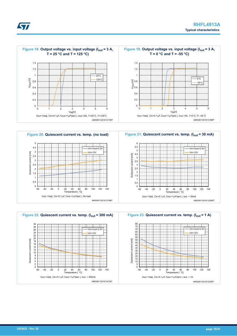
Figure 18. Output voltage vs. input voltage (Iout = 3 A,T = 25 °C and T = 125 °C)
Vout =Vadj, Cin=0.1μF, Cout=1μF(tant ), Iout =3A, T=25°C, T=125°C
0
0.2
0.4
0.6
0.8
1
1.2
1.4
0 1 2 3 4 5 6
V OU
T [V
]
VIN [V]
25°C
125°C
AMG081120161317MT
Figure 19. Output voltage vs. input voltage (Iout = 3 A,T = 0 °C and T = -55 °C)
Vout =Vadj , Cin=0.1 μF, Cout =1μF(tant ), Iout =3A, T=0°C, T= -55°C
0
0.2
0.4
0.6
0.8
1
1.2
1.4
0 1 2 3 4 5 6
VO
UT
[V]
VIN [V]
0°C
-55°C
AMG081120161318MT
Figure 20. Quiescent current vs. temp. (no load)
Vout =Vadj , Cin=0.1 μF, Cout =1μF(tant ), No load
0
0.5
1
1.5
2
2.5
3
3.5
4
4.5
5
-60 -40 -20 0 20 40 60 80 100 120 140
Qui
esce
nt c
urre
nt [m
A]
Temperature [ °C]
Vin=Vout+2.5V
Vin=12V
AMG081120161319MT
Figure 21. Quiescent current vs. temp. (Iout = 30 mA)
Vout =Vadj , Cin=0.1 μF, Cout =1μF(tant ), Iout = 30mA
00.5
11.5
22.5
33.5
44.5
55.5
6
-60 -40 -20 0 20 40 60 80 100 120 140
Qui
esce
nt c
urre
nt [m
A]
Temperature [ °C]
Vin=Vout+2.5V
Vin=12V
AMG081120161320MT
Figure 22. Quiescent current vs. temp. (Iout = 300 mA)
Vout =Vadj , Cin=0.1 μF, Cout =1μF(tant ), Iout = 300mA
02468
1012141618202224262830
-60 -40 -20 0 20 40 60 80 100 120 140
Qui
esce
nt c
urre
nt [m
A]
Temperature [ °C]
Vin=Vout+2.5V
Vin=12V
AMG081120161321MT
Figure 23. Quiescent current vs. temp. (Iout = 1 A)
Vout =Vadj , Cin=0.1 μF, Cout =1μF(tant ), Iout = 1A
05
101520253035404550556065707580
-60 -40 -20 0 20 40 60 80 100 120 140
Qui
esce
nt c
urre
nt [m
A]
Temperature [ °C]
Vin=Vout+2.5V
Vin=12V
AMG081120161322MT
RHFL4913ATypical characteristics
DS3625 - Rev 20 page 15/31

Figure 24. Quiescent current vs. temp. (Iout = 2 A)
Vout =Vadj , Cin=0.1 μF, Cout =1μF(tant ), Iout = 1A
05
101520253035404550556065707580
-60 -40 -20 0 20 40 60 80 100 120 140
Qui
esce
nt c
urre
nt [m
A]
Temperature [ °C]
Vin=Vout+2.5V
Vin=12V
AMG081120161323MT
Figure 25. Quiescent current vs. load current,(Vin = Vout + 2.5 V)
Vin=Vout+2.5V, Vout =Vadj , Cin=0.1μF, Cout =1μF(tant )
0
20
40
60
80
100
120
140
0 0.5 1 1.5 2 2.5
Qui
esce
nt c
urre
nt [m
A]
Load current [A]
-55°C
25°C
125°C
AMG081120161324MT
Figure 26. Quiescent current vs. load current, (Vin = 12 V)
Vin=12V, Vout =Vadj, Cin=0.1μF, Cout=1μF(tant )
0
20
40
60
80
100
120
140
0 0.5 1 1.5 2 2.5
Qui
esce
nt c
urre
nt [m
A]
Load current [A]
-55°C25°C125°C
AMG081120161325MT
Figure 27. Dropout voltage vs. temp. (Vout = 3 V, no load)
Vout = 3V, Cin=0.1μF, Cout=1μF(tant), No Load
5060708090
100110120130140150160170180190200
-60 -40 -20 0 20 40 60 80 100 120 140
Dro
pout
vol
tage
[mV]
Temperature [°C]
AMG081120161326MT
Figure 28. Dropout voltage vs. temp. (Vout = 3 V,Iout = 400 mA)
Vout = 3V, Cin=0.1μF, Cout=1μF(tant), Iout =400mA
200220240260280300320340360380400420440460480500
-60 -40 -20 0 20 40 60 80 100 120 140
Dro
pout
vol
tage
[mV]
Temperature [°C]
AMG081120161327MT
Figure 29. Dropout voltage vs. temp. (Vout = 3 V, Iout = 1 A)
Vout = 3V, Cin=0.1μF, Cout=1μF(tant), Iout =1A
200240280320360400440480520560600640680720760800
-60 -40 -20 0 20 40 60 80 100 120 140
Dro
pout
vol
tage
[mV]
Temperature [°C]
AMG081120161328MT
RHFL4913ATypical characteristics
DS3625 - Rev 20 page 16/31

Figure 30. Dropout voltage vs. temp. (Vout = 3 V, Iout= 2 A)
Vout = 3V, Cin=0.1μF, Cout=1μF(tant), Iout =2A
450500550600650700750800850900950
1000105011001150120012501300
-60 -40 -20 0 20 40 60 80 100 120 140
Dro
pout
vol
tage
[mV]
Temperature [°C]
AMG081120161329MT
Figure 31. Dropout voltage vs. temp. (Vout = 3 V, Iout= 3 A)
Vout = 3V, Cin=0.1μF, Cout=1μF(tant), Iout =3A
400450500550600650700750800850900950
100010501100115012001250130013501400
-60 -40 -20 0 20 40 60 80 100 120 140
Dro
pout
vol
tage
[mV]
Temperature [°C]
AMG081120161330MT
Figure 32. Dropout voltage vs. load current (Vout = 3 V)
Vout=3V, Cin=0.1μF, Cout=1μF(tant )
0
200
400
600
800
1000
1200
1400
0 0.5 1 1.5 2 2.5 3 3.5
Drop
out v
olta
ge [m
V]
Output current [A]
-55°C25°C125°C
AMG081120161331MT
Figure 33. Dropout voltage vs. load current (Vout = 9 V)
Vout =9V, Cin=0.1 μF, Cout =1μF(tant )
0
200
400
600
800
1000
1200
1400
0 0.5 1 1.5 2 2.5 3 3.5
Drop
out v
olta
ge [m
V]
Output current [A]
-55°C
25°C
125°C
AMG081120161332MT
Figure 34. SVR vs. frequency
0
10
20
30
40
50
60
70
80
10 100 1000 10000 100000 1000000
SVR
[dB]
Frequency [Hz]
Vout=VadjVout=3VVout=9V
Vripple = ± 1V, Cin=0.1μF, Cout=1μF(tant ), Iout=5mA, T=25°C
AMG081120161333MT
Figure 35. SVR vs. load current
20
30
40
50
60
70
80
0 0.5 1 1.5 2 2.5 3 3.5
SVR
[dB
]
Output current [A]
Vout=Vadj
Vout=3V
Vout=9V
Vripple= ± 1V, Cin=0.1µF, Cout=1µF(tant), T25°C, F=120Hz
AMG081120161334MT
RHFL4913ATypical characteristics
DS3625 - Rev 20 page 17/31
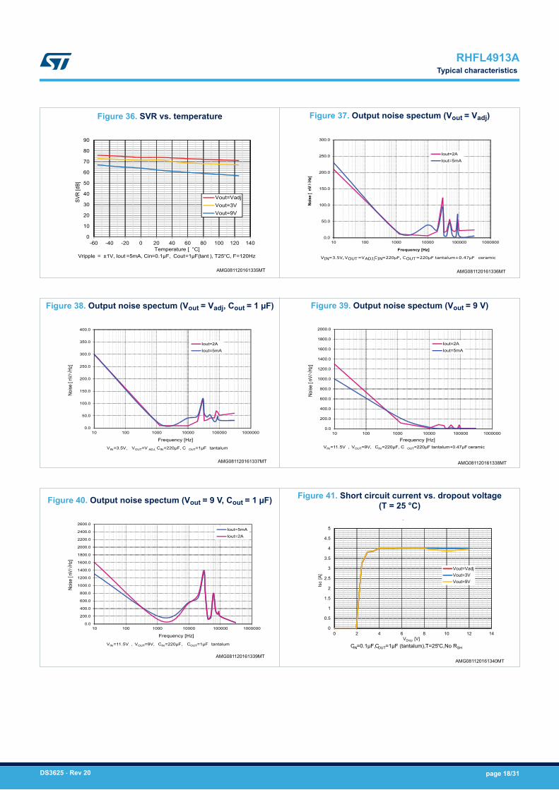
Figure 36. SVR vs. temperature
Vripple = ±1V, Iout =5mA, Cin=0.1µF, Cout=1µF(tant ), T25°C, F=120Hz
0
10
20
30
40
50
60
70
80
90
-60 -40 -20 0 20 40 60 80 100 120 140
SVR
[dB]
Temperature [ °C]
Vout=VadjVout=3VVout=9V
AMG081120161335MT
Figure 37. Output noise spectum (Vout = Vadj)
0.0
50.0
100.0
150.0
200.0
250.0
300.0
10 100 1000 10000 100000 1000000
Nois
e [nV
/√Hz
]
Frequency [Hz]
Iout=2AIout=5mA
VIN=3.5V, VOUT=VADJ, CIN=220µF, COUT=220µF tantalum+0.47µF ceramic
AMG081120161336MT
Figure 38. Output noise spectum (Vout = Vadj, Cout = 1 µF)
0.0
50.0
100.0
150.0
200.0
250.0
300.0
350.0
400.0
10 100 1000 10000 100000 1000000
Noise
[nV/√H
z]
Frequency [Hz]
Iout=2AIout=5mA
VIN=3.5V, VOUT=V ADJ, CIN=220µF, C OUT=1µF tantalum
AMG081120161337MT
Figure 39. Output noise spectum (Vout = 9 V)
0.0
200.0
400.0
600.0
800.0
1000.0
1200.0
1400.0
1600.0
1800.0
2000.0
10 100 1000 10000 100000 1000000
Noise
[nV
/√Hz
]
Frequency [Hz]
Iout=2AIout=5mA
VIN=11.5V , VOUT=9V, CIN=220µF, C OUT=220µF tantalum+0.47µF ceramic
AMG081120161338MT
Figure 40. Output noise spectum (Vout = 9 V, Cout = 1 µF)
0.0
200.0
400.0
600.0
800.0
1000.0
1200.0
1400.0
1600.0
1800.0
2000.0
2200.0
2400.0
2600.0
10 100 1000 10000 100000 1000000
Noise
[nV/√H
z]
Frequency [Hz]
Iout=5mA
Iout=2A
VIN=11.5V , VOUT=9V, CIN=220µF, COUT=1µF tantalum
AMG081120161339MT
Figure 41. Short circuit current vs. dropout voltage(T = 25 °C)
0
0.5
1
1.5
2
2.5
3
3.5
4
4.5
5
0 2 4 6 8 10 12 14
Isc
[A]
VDrop [V]
Vout=VadjVout=3VVout=9V
CIN=0.1µF, COUT=1µF (tantalum), T=25°C,No RSH
AMG081120161340MT
RHFL4913ATypical characteristics
DS3625 - Rev 20 page 18/31

Figure 42. Short circuit current vs. dropout voltage(T = 125 °C)
0
0.5
1
1.5
2
2.5
3
3.5
4
4.5
5
0 2 4 6 8 10 12 14
Isc
[A]
VDrop [V]
Vout=VadjVout=3VVout=9V
CIN=0.1µF, COUT=1µF (tantalum), T=125 °C,No RSH
AMG081120161341MT
Figure 43. Short circuit current vs. dropout voltage(T = -55 °C)
0
0.5
1
1.5
2
2.5
3
3.5
4
4.5
5
0 2 4 6 8 10 12 14
Isc
[A]
VDrop [V]
Vout=VadjVout=3VVout=9V
CIN=0.1µF, COUT=1µF (tantalum), T=-55°C,No R SH
AMG081120161342MT
Figure 44. Short circuit current vs. RSH
0
0.5
1
1.5
2
2.5
3
3.5
4
0 50 100 150 200 250 300
Isc
[A]
RSH [Kohm ]
Vout=Vadj
Vout=3V
Vout=9V
CIN=0.1µF, COUT=1µF (tantalum)
AMG081120161343MT
Figure 45. Short circuit current vs. RSH (zoom)
0
0.5
1
1.5
2
2.5
3
3.5
4
5 15 25 35 45 55 65
Isc
[A]
RSH [Kohm ]
Vout=Vadj
Vout=3V
Vout=9V
CIN=0.1µF, COUT=1µF (tantalum)
AMG081120161344MT
Figure 46. Enable turn-on/off (Vout = 9 V)
IN OUT=1µF; r
VOUT-
VINH
VIN=12V; VINH from 0V to 2V; VOUT= 9V; IOUT=5mAC =C T =Tf=5µs
AMG081120161345MT
Figure 47. Enable turn-on/off (Vout = 1.5 V)
VIN=4V; VINH from 0V to 2V; VOUT= 1.5V; IOUT=5mACIN=COUT=1µF; Tr=Tf=5µs
VOUT
VINH
AMG081120161346MT
RHFL4913ATypical characteristics
DS3625 - Rev 20 page 19/31

Figure 48. Turn-on time (Vout = 1.5 V)
VIN from 0 to 12V, VEN=GND, VOUT= 1.5V ,IOUT=5 mA, CIN=COUT=1µF Tf=5µs
VOUT
VIN
AMG081120161347MT
Figure 49. Turn-on time (Vout = 9 V)
VIN from 0 to 12V, VEN=GND, VOUT= 9V ,IOUT=5 mA, CIN=COUT=1µF Tf=5µs
VOUT
VIN
AMG081120161348MT
Figure 50. Inhibit propagation delay (Lo-Hi)
VIN=5.5V, VINH=from 2.4V to 0V, IOUT=400mA,VOUT=3V,CIN=COUT=1µF, Tf=0.5µs
VOUT
VINH
IOUT
AMG081120161349MT
Figure 51. Inhibit propagation delay (Hi-Lo)
VIN=5.5V, VINH=from 0V to 2.4V, IOUT=400mA,VOUT=3V,CIN=COUT=1µF, Tr=0.5µs
VOUT
VINH
IOUT
AMG081120161350MT
Figure 52. Line transient
VIN=from 3.8 to 12V, VOUT=VADJ, IOUT=10mA, COUT=1µF , Tr=5µs
VOUT(AC)
VIN
AMG081120161351MT
Figure 53. Load transient
VIN= 3.8V, VOUT=VADJ, IOUT= from 0 to 800mA, COUT=1µF , Tf=5µs
VOUT(AC)
IOUT
AMG081120161352MT
RHFL4913ATypical characteristics
DS3625 - Rev 20 page 20/31

Figure 54. Stability plan (Vout = Vadj)
VIN from 3 to 12V; I OUT from 5mA to 2A; V OUT= VADJ; C IN=1µF ; T=25 ° C
0.001
0.01
0.1
1
10
100
1 10 100
ES
R @
10
0 kH
z [Ω
]
COUT[µF] (nominal value)
STABILITY AREA
AMG081120161353MT
RHFL4913ATypical characteristics
DS3625 - Rev 20 page 21/31
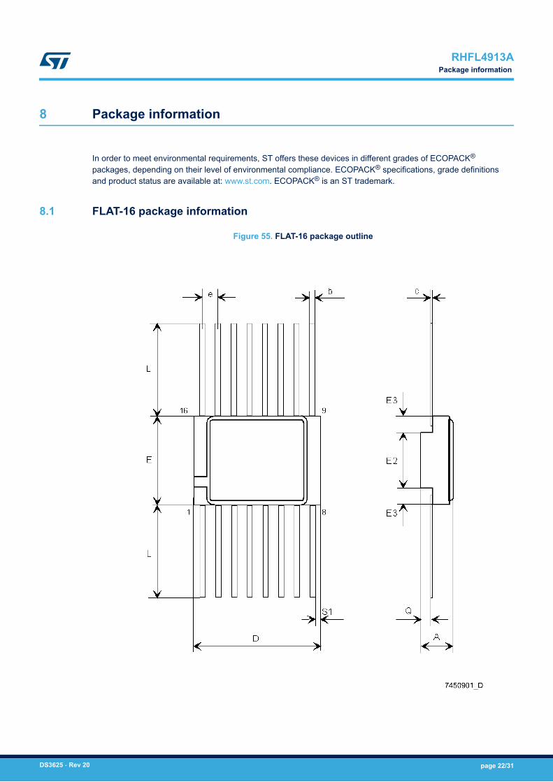
8 Package information
In order to meet environmental requirements, ST offers these devices in different grades of ECOPACK®
packages, depending on their level of environmental compliance. ECOPACK® specifications, grade definitionsand product status are available at: www.st.com. ECOPACK® is an ST trademark.
8.1 FLAT-16 package information
Figure 55. FLAT-16 package outline
RHFL4913APackage information
DS3625 - Rev 20 page 22/31

Table 5. FLAT-16 package mechanical data
Dim.mm
Min. Typ. Max.
A 2.42 2.88
b 0.38 0.48
c 0.10 0.18
D 9.71 10.11
E 6.71 7.11
E2 3.30 3.45 3.60
E3 0.76
e 1.27
L 6.35 7.36
Q 0.66 1.14
S1 0.13
RHFL4913AFlat-16 package information
DS3625 - Rev 20 page 23/31

8.2 SMD5C package information
Figure 56. SMD5C package outline
Table 6. SMD5C package mechanical data
Dim.mm
Min. Typ. Max.
A 2.99 3.15 3.30
A1 0.25 0.38 0.51
b 7.13 7.26 7.39
b1 4.95 5.08 5.21
b2 2.28 2.41 2.54
b3 2.92 3.05 3.18
D 13.71 13.84 13.97
D1 0.76
E 7.39 7.52 7.65
e 1.91
RHFL4913A
DS3625 - Rev 20 page 24/31

9 Ordering information
Table 7. Device summary
Order code Generic SMD(1) Quality Package Lead
finish Vin range Iout(max) Temperature range
RHFL4913SCA1
5962F02524
Engineeringmodel SMD5C Gold
3 to 12 Volt
3.0
-55 to 150 °C
RHFL4913SCA07V Flight model
RHFL4913KPA1 Engineeringmodel
Flat-16PGold
2.0RHFL4913KPA-01V Flight model
RHFL4913KPA-02V Flight model SolderDip
1. Standard microcircuit drawing
Table 8. Ordering information
Order code (1) SMD pin Quality level Package Leadfinish Marking (2) Mass Packing
RHFL4913SCA1 - EngineeringModel SMD5C Gold
RHFL4913SCA12.5 g
Strip pack
RHFL4913KPA1 5962F0252403VUC QML-V 5962F0252403VUC
RHFL4913KPA1 - EngineeringModel
Flat-16PGold
RHFL4913KPA1
0.6 gRHFL4913KPA-01V 5962F0252401VXC QML-V 5962F0252401VXC
RHFL4913KPA-02V 5962F0252401VXA QML-V Solder Dip 5962F0252401VXA
1. Contact ST sales office for information about the specific conditions for:• Products in die form• Other quality levels
• Tape and reel packing2. Specific marking only. The full marking includes in addition:
• For the engineering models : ST logo, date code, country of origin (FR)• For ESCC flight parts : ST logo, date code, country of origin (FR), manufacturer code (CSTM), serial number of the
part within the assembly lot
Table 9. Environmental characteristics
Parameter Conditions Value Unit
Output voltage thermal drift -55°C to +125°C 40 ppm/°C
Output voltage radiation drift From 0 krad to 300 krad at 0.55 rad/s 8 ppm/krad
Output voltage radiation drift From 0 krad to 300 krad, Mil Std 883E Method 1019.6 6 ppm/krad
RHFL4913AOrdering information
DS3625 - Rev 20 page 25/31

Revision history
Table 10. Document revision history
Date Revision Changes
29-Oct-2004 3 New order codes added - Tables 4 and 5.
27-May-2005 4 Features, Tables 4, 5 and the Figure 1 has been updated. Add theMechanical Data SOC-16.
08-Jun-2005 5 Mistake on Table 4 (Q.ty Level), Table 7 has been updated and add DIEInformation.
30-Jan-2006 6 Added new package SMD5C and removed old package SOC-16.
26-Jan-2007 7 DIE Information and DIE Pad has been updated par. 6, pages 9 and 10.
23-Nov-2007 8 Pin information for the SMD5C package updated in Table 1; added section6.3: FPGA power supply lines on page 10. Minor text changes.
22-Sep-2008 9 Modified Application information on page 9.
17-Nov-2008 10 Modified Table 8 on page 26.
21-Jan-2010 11 Modified Table 7 on page 26.
18-Oct-2010 12 Modified Section 6.2 on page 9.
07-Feb-2011 13 Added: note Table 1 on page 3.
07-Dec-2011 14 Removed the note under Table 1 on page 3 and added footnotes 1 and 2.
20-Aug-2012 15 Order code updated in Table 7 on page 26 about the SMD5C package
15-Jan-2014 16
Updated Features in cover page.
Added Section 7: Typical characteristics.
Modified Table 4: Electrical characteristics.
Updated Section 9: Package mechanical data and Section 10: Orderinginformation.
Minor text changes.
05-May-2014 17Updated Figure 18: Output voltage vs input voltage (Iout=3 A, T=25 °C andT=125 °C).
Minor text changes.
22-Nov-2016 18
Updated description in cover page.
Updated Section 9: "Package information".
Minor text changes.
30-Mar-2018 19
Updated:
- Figure 5. Baseline bias configuration with remote feedback and Figure 6.Local feedback configuration.
- Section 6.4 Notes on the 16-pin hermetic package.
- Section 9 Ordering information.
27-Apr-2018 20 Updated: Section 3 Maximum ratings.
RHFL4913A
DS3625 - Rev 20 page 26/31

Contents
1 Diagram . . . . . . . . . . . . . . . . . . . . . . . . . . . . . . . . . . . . . . . . . . . . . . . . . . . . . . . . . . . . . . . . . . . . . . . . . . .2
2 Pin configuration . . . . . . . . . . . . . . . . . . . . . . . . . . . . . . . . . . . . . . . . . . . . . . . . . . . . . . . . . . . . . . . . . .3
3 Maximum ratings . . . . . . . . . . . . . . . . . . . . . . . . . . . . . . . . . . . . . . . . . . . . . . . . . . . . . . . . . . . . . . . . . .4
4 Electrical characteristics. . . . . . . . . . . . . . . . . . . . . . . . . . . . . . . . . . . . . . . . . . . . . . . . . . . . . . . . . . .5
5 Device description. . . . . . . . . . . . . . . . . . . . . . . . . . . . . . . . . . . . . . . . . . . . . . . . . . . . . . . . . . . . . . . . .9
5.1 ADJ pin. . . . . . . . . . . . . . . . . . . . . . . . . . . . . . . . . . . . . . . . . . . . . . . . . . . . . . . . . . . . . . . . . . . . . . . 9
5.2 Inhibit ON-OFF control . . . . . . . . . . . . . . . . . . . . . . . . . . . . . . . . . . . . . . . . . . . . . . . . . . . . . . . . . . 9
5.3 Overtemperature protection . . . . . . . . . . . . . . . . . . . . . . . . . . . . . . . . . . . . . . . . . . . . . . . . . . . . . . 9
5.4 Programmable overcurrent protection . . . . . . . . . . . . . . . . . . . . . . . . . . . . . . . . . . . . . . . . . . . . . 9
5.5 OCM pin . . . . . . . . . . . . . . . . . . . . . . . . . . . . . . . . . . . . . . . . . . . . . . . . . . . . . . . . . . . . . . . . . . . . . . 9
6 Application information. . . . . . . . . . . . . . . . . . . . . . . . . . . . . . . . . . . . . . . . . . . . . . . . . . . . . . . . . . .10
6.1 Output capacitor selection and stability. . . . . . . . . . . . . . . . . . . . . . . . . . . . . . . . . . . . . . . . . . . . 10
6.2 Remote sensing operation . . . . . . . . . . . . . . . . . . . . . . . . . . . . . . . . . . . . . . . . . . . . . . . . . . . . . . 10
6.3 FPGA power supply lines. . . . . . . . . . . . . . . . . . . . . . . . . . . . . . . . . . . . . . . . . . . . . . . . . . . . . . . 10
6.4 Notes on the 16-pin hermetic package. . . . . . . . . . . . . . . . . . . . . . . . . . . . . . . . . . . . . . . . . . . . 12
7 Typical characteristics . . . . . . . . . . . . . . . . . . . . . . . . . . . . . . . . . . . . . . . . . . . . . . . . . . . . . . . . . . . .13
8 Package information. . . . . . . . . . . . . . . . . . . . . . . . . . . . . . . . . . . . . . . . . . . . . . . . . . . . . . . . . . . . . .22
8.1 FLAT-16 package information . . . . . . . . . . . . . . . . . . . . . . . . . . . . . . . . . . . . . . . . . . . . . . . . . . . 22
8.2 SMD5C package information. . . . . . . . . . . . . . . . . . . . . . . . . . . . . . . . . . . . . . . . . . . . . . . . . . . . 24
9 Ordering information . . . . . . . . . . . . . . . . . . . . . . . . . . . . . . . . . . . . . . . . . . . . . . . . . . . . . . . . . . . . .25
Revision history . . . . . . . . . . . . . . . . . . . . . . . . . . . . . . . . . . . . . . . . . . . . . . . . . . . . . . . . . . . . . . . . . . . . . . .26
Contents . . . . . . . . . . . . . . . . . . . . . . . . . . . . . . . . . . . . . . . . . . . . . . . . . . . . . . . . . . . . . . . . . . . . . . . . . . . . . .27
List of tables . . . . . . . . . . . . . . . . . . . . . . . . . . . . . . . . . . . . . . . . . . . . . . . . . . . . . . . . . . . . . . . . . . . . . . . . . .28
List of figures. . . . . . . . . . . . . . . . . . . . . . . . . . . . . . . . . . . . . . . . . . . . . . . . . . . . . . . . . . . . . . . . . . . . . . . . . .29
RHFL4913AContents
DS3625 - Rev 20 page 27/31
List of tablesTable 1. Pin description. . . . . . . . . . . . . . . . . . . . . . . . . . . . . . . . . . . . . . . . . . . . . . . . . . . . . . . . . . . . . . . . . . . . . . 3Table 2. Recommended maximum operating ratings. . . . . . . . . . . . . . . . . . . . . . . . . . . . . . . . . . . . . . . . . . . . . . . . . . 4Table 3. Thermal data. . . . . . . . . . . . . . . . . . . . . . . . . . . . . . . . . . . . . . . . . . . . . . . . . . . . . . . . . . . . . . . . . . . . . . . 4Table 4. Electrical characteristics . . . . . . . . . . . . . . . . . . . . . . . . . . . . . . . . . . . . . . . . . . . . . . . . . . . . . . . . . . . . . . . 5Table 5. FLAT-16 package mechanical data. . . . . . . . . . . . . . . . . . . . . . . . . . . . . . . . . . . . . . . . . . . . . . . . . . . . . . . 23Table 6. SMD5C package mechanical data . . . . . . . . . . . . . . . . . . . . . . . . . . . . . . . . . . . . . . . . . . . . . . . . . . . . . . . 24Table 7. Device summary . . . . . . . . . . . . . . . . . . . . . . . . . . . . . . . . . . . . . . . . . . . . . . . . . . . . . . . . . . . . . . . . . . . 25Table 8. Ordering information. . . . . . . . . . . . . . . . . . . . . . . . . . . . . . . . . . . . . . . . . . . . . . . . . . . . . . . . . . . . . . . . . 25Table 9. Environmental characteristics . . . . . . . . . . . . . . . . . . . . . . . . . . . . . . . . . . . . . . . . . . . . . . . . . . . . . . . . . . 25Table 10. Document revision history . . . . . . . . . . . . . . . . . . . . . . . . . . . . . . . . . . . . . . . . . . . . . . . . . . . . . . . . . . . . . 26
RHFL4913AList of tables
DS3625 - Rev 20 page 28/31

List of figuresFigure 1. Block diagram . . . . . . . . . . . . . . . . . . . . . . . . . . . . . . . . . . . . . . . . . . . . . . . . . . . . . . . . . . . . . . . . . . . . 2Figure 2. Pin configuration (top view for FLAT-16, bottom view for SMD5C) . . . . . . . . . . . . . . . . . . . . . . . . . . . . . . . . . 3Figure 3. Application diagram for remote sensing operation . . . . . . . . . . . . . . . . . . . . . . . . . . . . . . . . . . . . . . . . . . . . 8Figure 4. Baseline bias configuration with remote feedback . . . . . . . . . . . . . . . . . . . . . . . . . . . . . . . . . . . . . . . . . . . 11Figure 5. Local feedback configuration . . . . . . . . . . . . . . . . . . . . . . . . . . . . . . . . . . . . . . . . . . . . . . . . . . . . . . . . . 11Figure 6. Reference voltage vs. temp. (Vin = Vout + 2.5 V) . . . . . . . . . . . . . . . . . . . . . . . . . . . . . . . . . . . . . . . . . . . . 13Figure 7. Reference voltage vs. temp. (Vin = 12 V) . . . . . . . . . . . . . . . . . . . . . . . . . . . . . . . . . . . . . . . . . . . . . . . . . 13Figure 8. Reference voltage vs. temp. (Vin = Vout + 2.5 V, Iout = 1 A) . . . . . . . . . . . . . . . . . . . . . . . . . . . . . . . . . . . . . 13Figure 9. Reference voltage vs. temp. (Vin = 12 V, Iout= 1 A). . . . . . . . . . . . . . . . . . . . . . . . . . . . . . . . . . . . . . . . . . . 13Figure 10. Reference voltage vs. temp. (Vin = Vout + 2.5 V, Iout = 2 A) . . . . . . . . . . . . . . . . . . . . . . . . . . . . . . . . . . . . . 13Figure 11. Reference voltage vs. temp. (Vin = 12 V, Iout= 2 A). . . . . . . . . . . . . . . . . . . . . . . . . . . . . . . . . . . . . . . . . . . 13Figure 12. Line regulation vs. temperature. . . . . . . . . . . . . . . . . . . . . . . . . . . . . . . . . . . . . . . . . . . . . . . . . . . . . . . . 14Figure 13. Load regulation vs. temp. (Iout = 5 mA to 400 mA) . . . . . . . . . . . . . . . . . . . . . . . . . . . . . . . . . . . . . . . . . . . 14Figure 14. Load regulation vs. temp. (Iout = 5 mA to 1 A) . . . . . . . . . . . . . . . . . . . . . . . . . . . . . . . . . . . . . . . . . . . . . . 14Figure 15. Inhibit threshold vs. temperature . . . . . . . . . . . . . . . . . . . . . . . . . . . . . . . . . . . . . . . . . . . . . . . . . . . . . . . 14Figure 16. Output voltage vs. input voltage (Iout = 0 mA, T = 25 °C and T = 125 °C) . . . . . . . . . . . . . . . . . . . . . . . . . . . 14Figure 17. Output voltage vs. input voltage (Iout = 0 mA, T = 0 °C and T = -55 °C). . . . . . . . . . . . . . . . . . . . . . . . . . . . . 14Figure 18. Output voltage vs. input voltage (Iout = 3 A, T = 25 °C and T = 125 °C). . . . . . . . . . . . . . . . . . . . . . . . . . . . . 15Figure 19. Output voltage vs. input voltage (Iout = 3 A, T = 0 °C and T = -55 °C) . . . . . . . . . . . . . . . . . . . . . . . . . . . . . . 15Figure 20. Quiescent current vs. temp. (no load) . . . . . . . . . . . . . . . . . . . . . . . . . . . . . . . . . . . . . . . . . . . . . . . . . . . 15Figure 21. Quiescent current vs. temp. (Iout = 30 mA) . . . . . . . . . . . . . . . . . . . . . . . . . . . . . . . . . . . . . . . . . . . . . . . . 15Figure 22. Quiescent current vs. temp. (Iout = 300 mA) . . . . . . . . . . . . . . . . . . . . . . . . . . . . . . . . . . . . . . . . . . . . . . . 15Figure 23. Quiescent current vs. temp. (Iout = 1 A) . . . . . . . . . . . . . . . . . . . . . . . . . . . . . . . . . . . . . . . . . . . . . . . . . . 15Figure 24. Quiescent current vs. temp. (Iout = 2 A) . . . . . . . . . . . . . . . . . . . . . . . . . . . . . . . . . . . . . . . . . . . . . . . . . . 16Figure 25. Quiescent current vs. load current, (Vin = Vout + 2.5 V). . . . . . . . . . . . . . . . . . . . . . . . . . . . . . . . . . . . . . . . 16Figure 26. Quiescent current vs. load current, (Vin = 12 V) . . . . . . . . . . . . . . . . . . . . . . . . . . . . . . . . . . . . . . . . . . . . . 16Figure 27. Dropout voltage vs. temp. (Vout = 3 V, no load) . . . . . . . . . . . . . . . . . . . . . . . . . . . . . . . . . . . . . . . . . . . . . 16Figure 28. Dropout voltage vs. temp. (Vout = 3 V, Iout = 400 mA) . . . . . . . . . . . . . . . . . . . . . . . . . . . . . . . . . . . . . . . . . 16Figure 29. Dropout voltage vs. temp. (Vout = 3 V, Iout = 1 A) . . . . . . . . . . . . . . . . . . . . . . . . . . . . . . . . . . . . . . . . . . . . 16Figure 30. Dropout voltage vs. temp. (Vout = 3 V, Iout= 2 A) . . . . . . . . . . . . . . . . . . . . . . . . . . . . . . . . . . . . . . . . . . . . 17Figure 31. Dropout voltage vs. temp. (Vout = 3 V, Iout= 3 A) . . . . . . . . . . . . . . . . . . . . . . . . . . . . . . . . . . . . . . . . . . . . 17Figure 32. Dropout voltage vs. load current (Vout = 3 V). . . . . . . . . . . . . . . . . . . . . . . . . . . . . . . . . . . . . . . . . . . . . . . 17Figure 33. Dropout voltage vs. load current (Vout = 9 V). . . . . . . . . . . . . . . . . . . . . . . . . . . . . . . . . . . . . . . . . . . . . . . 17Figure 34. SVR vs. frequency . . . . . . . . . . . . . . . . . . . . . . . . . . . . . . . . . . . . . . . . . . . . . . . . . . . . . . . . . . . . . . . . 17Figure 35. SVR vs. load current . . . . . . . . . . . . . . . . . . . . . . . . . . . . . . . . . . . . . . . . . . . . . . . . . . . . . . . . . . . . . . . 17Figure 36. SVR vs. temperature . . . . . . . . . . . . . . . . . . . . . . . . . . . . . . . . . . . . . . . . . . . . . . . . . . . . . . . . . . . . . . . 18Figure 37. Output noise spectum (Vout = Vadj) . . . . . . . . . . . . . . . . . . . . . . . . . . . . . . . . . . . . . . . . . . . . . . . . . . . . . 18Figure 38. Output noise spectum (Vout = Vadj, Cout = 1 µF). . . . . . . . . . . . . . . . . . . . . . . . . . . . . . . . . . . . . . . . . . . . . 18Figure 39. Output noise spectum (Vout = 9 V). . . . . . . . . . . . . . . . . . . . . . . . . . . . . . . . . . . . . . . . . . . . . . . . . . . . . . 18Figure 40. Output noise spectum (Vout = 9 V, Cout = 1 µF) . . . . . . . . . . . . . . . . . . . . . . . . . . . . . . . . . . . . . . . . . . . . . 18Figure 41. Short circuit current vs. dropout voltage (T = 25 °C). . . . . . . . . . . . . . . . . . . . . . . . . . . . . . . . . . . . . . . . . . 18Figure 42. Short circuit current vs. dropout voltage (T = 125 °C) . . . . . . . . . . . . . . . . . . . . . . . . . . . . . . . . . . . . . . . . . 19Figure 43. Short circuit current vs. dropout voltage (T = -55 °C) . . . . . . . . . . . . . . . . . . . . . . . . . . . . . . . . . . . . . . . . . 19Figure 44. Short circuit current vs. RSH . . . . . . . . . . . . . . . . . . . . . . . . . . . . . . . . . . . . . . . . . . . . . . . . . . . . . . . . . 19Figure 45. Short circuit current vs. RSH (zoom). . . . . . . . . . . . . . . . . . . . . . . . . . . . . . . . . . . . . . . . . . . . . . . . . . . . . 19Figure 46. Enable turn-on/off (Vout = 9 V) . . . . . . . . . . . . . . . . . . . . . . . . . . . . . . . . . . . . . . . . . . . . . . . . . . . . . . . . 19Figure 47. Enable turn-on/off (Vout = 1.5 V) . . . . . . . . . . . . . . . . . . . . . . . . . . . . . . . . . . . . . . . . . . . . . . . . . . . . . . . 19Figure 48. Turn-on time (Vout = 1.5 V) . . . . . . . . . . . . . . . . . . . . . . . . . . . . . . . . . . . . . . . . . . . . . . . . . . . . . . . . . . . 20
RHFL4913AList of figures
DS3625 - Rev 20 page 29/31
Figure 49. Turn-on time (Vout = 9 V) . . . . . . . . . . . . . . . . . . . . . . . . . . . . . . . . . . . . . . . . . . . . . . . . . . . . . . . . . . . . 20Figure 50. Inhibit propagation delay (Lo-Hi) . . . . . . . . . . . . . . . . . . . . . . . . . . . . . . . . . . . . . . . . . . . . . . . . . . . . . . . 20Figure 51. Inhibit propagation delay (Hi-Lo) . . . . . . . . . . . . . . . . . . . . . . . . . . . . . . . . . . . . . . . . . . . . . . . . . . . . . . . 20Figure 52. Line transient . . . . . . . . . . . . . . . . . . . . . . . . . . . . . . . . . . . . . . . . . . . . . . . . . . . . . . . . . . . . . . . . . . . . 20Figure 53. Load transient . . . . . . . . . . . . . . . . . . . . . . . . . . . . . . . . . . . . . . . . . . . . . . . . . . . . . . . . . . . . . . . . . . . 20Figure 54. Stability plan (Vout = Vadj) . . . . . . . . . . . . . . . . . . . . . . . . . . . . . . . . . . . . . . . . . . . . . . . . . . . . . . . . . . . . 21Figure 55. FLAT-16 package outline . . . . . . . . . . . . . . . . . . . . . . . . . . . . . . . . . . . . . . . . . . . . . . . . . . . . . . . . . . . . 22Figure 56. SMD5C package outline . . . . . . . . . . . . . . . . . . . . . . . . . . . . . . . . . . . . . . . . . . . . . . . . . . . . . . . . . . . . 24
RHFL4913AList of figures
DS3625 - Rev 20 page 30/31

IMPORTANT NOTICE – PLEASE READ CAREFULLY
STMicroelectronics NV and its subsidiaries (“ST”) reserve the right to make changes, corrections, enhancements, modifications, and improvements to STproducts and/or to this document at any time without notice. Purchasers should obtain the latest relevant information on ST products before placing orders. STproducts are sold pursuant to ST’s terms and conditions of sale in place at the time of order acknowledgement.
Purchasers are solely responsible for the choice, selection, and use of ST products and ST assumes no liability for application assistance or the design ofPurchasers’ products.
No license, express or implied, to any intellectual property right is granted by ST herein.
Resale of ST products with provisions different from the information set forth herein shall void any warranty granted by ST for such product.
ST and the ST logo are trademarks of ST. All other product or service names are the property of their respective owners.
Information in this document supersedes and replaces information previously supplied in any prior versions of this document.
© 2018 STMicroelectronics – All rights reserved
RHFL4913A
DS3625 - Rev 20 page 31/31

![TL783 High-Voltage Adjustable Regulator datasheet (Rev. N) · TL783 High-Voltage Adjustable Regulator datasheet (Rev. N) Author: Texas Instruments, Incorporated [SLVS036,N ] Subject:](https://img.pdfslide.net/doc/110x75/60eb795745542b35e81e1928/tl783-high-voltage-adjustable-regulator-datasheet-rev-n-tl783-high-voltage-adjustable.jpg)