Embed Size (px)
Citation preview
Stellaris® LM3S601 Microcontroller
DATA SHEET
Copyr ight © 2007-2014Texas Instruments Incorporated
DS-LM3S601-15852.2743SPMS100I
TEXAS INSTRUMENTS-PRODUCTION DATA

CopyrightCopyright © 2007-2014 Texas Instruments Incorporated All rights reserved. Stellaris and StellarisWare® are registered trademarks of Texas InstrumentsIncorporated. ARM and Thumb are registered trademarks and Cortex is a trademark of ARM Limited. Other names and brands may be claimed as theproperty of others.
PRODUCTION DATA information is current as of publication date. Products conform to specifications per the terms of Texas Instruments standardwarranty. Production processing does not necessarily include testing of all parameters.
Please be aware that an important notice concerning availability, standard warranty, and use in critical applications of Texas Instruments semiconductorproducts and disclaimers thereto appears at the end of this data sheet.
Texas Instruments Incorporated108 Wild Basin, Suite 350Austin, TX 78746http://www.ti.com/stellarishttp://www-k.ext.ti.com/sc/technical-support/product-information-centers.htm
July 14, 20142Texas Instruments-Production Data
Table of ContentsRevision History ............................................................................................................................. 20About This Document .................................................................................................................... 24Audience .............................................................................................................................................. 24About This Manual ................................................................................................................................ 24Related Documents ............................................................................................................................... 24Documentation Conventions .................................................................................................................. 25
1 Architectural Overview .......................................................................................... 271.1 Product Features .......................................................................................................... 271.2 Target Applications ........................................................................................................ 341.3 High-Level Block Diagram ............................................................................................. 341.4 Functional Overview ...................................................................................................... 361.4.1 ARM Cortex™-M3 ......................................................................................................... 361.4.2 Motor Control Peripherals .............................................................................................. 371.4.3 Analog Peripherals ........................................................................................................ 381.4.4 Serial Communications Peripherals ................................................................................ 381.4.5 System Peripherals ....................................................................................................... 391.4.6 Memory Peripherals ...................................................................................................... 401.4.7 Additional Features ....................................................................................................... 401.4.8 Hardware Details .......................................................................................................... 411.4.9 System Block Diagram .................................................................................................. 42
2 The Cortex-M3 Processor ...................................................................................... 432.1 Block Diagram .............................................................................................................. 442.2 Overview ...................................................................................................................... 452.2.1 System-Level Interface .................................................................................................. 452.2.2 Integrated Configurable Debug ...................................................................................... 452.2.3 Trace Port Interface Unit (TPIU) ..................................................................................... 462.2.4 Cortex-M3 System Component Details ........................................................................... 462.3 Programming Model ...................................................................................................... 472.3.1 Processor Mode and Privilege Levels for Software Execution ........................................... 472.3.2 Stacks .......................................................................................................................... 472.3.3 Register Map ................................................................................................................ 482.3.4 Register Descriptions .................................................................................................... 492.3.5 Exceptions and Interrupts .............................................................................................. 622.3.6 Data Types ................................................................................................................... 622.4 Memory Model .............................................................................................................. 622.4.1 Memory Regions, Types and Attributes ........................................................................... 632.4.2 Memory System Ordering of Memory Accesses .............................................................. 642.4.3 Behavior of Memory Accesses ....................................................................................... 642.4.4 Software Ordering of Memory Accesses ......................................................................... 652.4.5 Bit-Banding ................................................................................................................... 662.4.6 Data Storage ................................................................................................................ 682.4.7 Synchronization Primitives ............................................................................................. 692.5 Exception Model ........................................................................................................... 702.5.1 Exception States ........................................................................................................... 712.5.2 Exception Types ............................................................................................................ 71
3July 14, 2014Texas Instruments-Production Data
Stellaris® LM3S601 Microcontroller
2.5.3 Exception Handlers ....................................................................................................... 742.5.4 Vector Table .................................................................................................................. 742.5.5 Exception Priorities ....................................................................................................... 752.5.6 Interrupt Priority Grouping .............................................................................................. 752.5.7 Exception Entry and Return ........................................................................................... 752.6 Fault Handling .............................................................................................................. 772.6.1 Fault Types ................................................................................................................... 782.6.2 Fault Escalation and Hard Faults .................................................................................... 782.6.3 Fault Status Registers and Fault Address Registers ........................................................ 792.6.4 Lockup ......................................................................................................................... 792.7 Power Management ...................................................................................................... 802.7.1 Entering Sleep Modes ................................................................................................... 802.7.2 Wake Up from Sleep Mode ............................................................................................ 802.8 Instruction Set Summary ............................................................................................... 81
3 Cortex-M3 Peripherals ........................................................................................... 853.1 Functional Description ................................................................................................... 853.1.1 System Timer (SysTick) ................................................................................................. 853.1.2 Nested Vectored Interrupt Controller (NVIC) .................................................................... 863.1.3 System Control Block (SCB) .......................................................................................... 883.1.4 Memory Protection Unit (MPU) ....................................................................................... 883.2 Register Map ................................................................................................................ 933.3 System Timer (SysTick) Register Descriptions ................................................................ 943.4 NVIC Register Descriptions ........................................................................................... 983.5 System Control Block (SCB) Register Descriptions ........................................................ 1063.6 Memory Protection Unit (MPU) Register Descriptions .................................................... 133
4 JTAG Interface ...................................................................................................... 1434.1 Block Diagram ............................................................................................................ 1444.2 Signal Description ....................................................................................................... 1444.3 Functional Description ................................................................................................. 1454.3.1 JTAG Interface Pins ..................................................................................................... 1454.3.2 JTAG TAP Controller ................................................................................................... 1464.3.3 Shift Registers ............................................................................................................ 1474.3.4 Operational Considerations .......................................................................................... 1474.4 Initialization and Configuration ..................................................................................... 1494.5 Register Descriptions .................................................................................................. 1494.5.1 Instruction Register (IR) ............................................................................................... 1494.5.2 Data Registers ............................................................................................................ 151
5 System Control ..................................................................................................... 1535.1 Signal Description ....................................................................................................... 1535.2 Functional Description ................................................................................................. 1535.2.1 Device Identification .................................................................................................... 1535.2.2 Reset Control .............................................................................................................. 1535.2.3 Power Control ............................................................................................................. 1585.2.4 Clock Control .............................................................................................................. 1585.2.5 System Control ........................................................................................................... 1615.3 Initialization and Configuration ..................................................................................... 1625.4 Register Map .............................................................................................................. 1635.5 Register Descriptions .................................................................................................. 164
July 14, 20144Texas Instruments-Production Data
Table of Contents
6 Internal Memory ................................................................................................... 2126.1 Block Diagram ............................................................................................................ 2126.2 Functional Description ................................................................................................. 2126.2.1 SRAM Memory ............................................................................................................ 2126.2.2 Flash Memory ............................................................................................................. 2136.3 Flash Memory Initialization and Configuration ............................................................... 2166.3.1 Changing Flash Protection Bits .................................................................................... 2166.3.2 Flash Programming ..................................................................................................... 2176.4 Register Map .............................................................................................................. 2186.5 Flash Register Descriptions (Flash Control Offset) ......................................................... 2186.6 Flash Register Descriptions (System Control Offset) ...................................................... 226
7 General-Purpose Input/Outputs (GPIOs) ........................................................... 2307.1 Block Diagram ............................................................................................................ 2317.2 Signal Description ....................................................................................................... 2317.3 Functional Description ................................................................................................. 2347.3.1 Data Control ............................................................................................................... 2357.3.2 Interrupt Control .......................................................................................................... 2367.3.3 Mode Control .............................................................................................................. 2377.3.4 Pad Control ................................................................................................................. 2377.3.5 Identification ............................................................................................................... 2377.4 Initialization and Configuration ..................................................................................... 2377.5 Register Map .............................................................................................................. 2387.6 Register Descriptions .................................................................................................. 240
8 General-Purpose Timers ...................................................................................... 2728.1 Block Diagram ............................................................................................................ 2738.2 Signal Description ....................................................................................................... 2738.3 Functional Description ................................................................................................. 2748.3.1 GPTM Reset Conditions .............................................................................................. 2748.3.2 32-Bit Timer Operating Modes ...................................................................................... 2748.3.3 16-Bit Timer Operating Modes ...................................................................................... 2758.4 Initialization and Configuration ..................................................................................... 2798.4.1 32-Bit One-Shot/Periodic Timer Mode ........................................................................... 2798.4.2 32-Bit Real-Time Clock (RTC) Mode ............................................................................. 2808.4.3 16-Bit One-Shot/Periodic Timer Mode ........................................................................... 2808.4.4 16-Bit Input Edge Count Mode ..................................................................................... 2818.4.5 16-Bit Input Edge Timing Mode .................................................................................... 2818.4.6 16-Bit PWM Mode ....................................................................................................... 2828.5 Register Map .............................................................................................................. 2828.6 Register Descriptions .................................................................................................. 283
9 Watchdog Timer ................................................................................................... 3089.1 Block Diagram ............................................................................................................ 3099.2 Functional Description ................................................................................................. 3099.3 Initialization and Configuration ..................................................................................... 3109.4 Register Map .............................................................................................................. 3109.5 Register Descriptions .................................................................................................. 311
10 Universal Asynchronous Receivers/Transmitters (UARTs) ............................. 33210.1 Block Diagram ............................................................................................................ 333
5July 14, 2014Texas Instruments-Production Data
Stellaris® LM3S601 Microcontroller
10.2 Signal Description ....................................................................................................... 33310.3 Functional Description ................................................................................................. 33410.3.1 Transmit/Receive Logic ............................................................................................... 33410.3.2 Baud-Rate Generation ................................................................................................. 33410.3.3 Data Transmission ...................................................................................................... 33510.3.4 FIFO Operation ........................................................................................................... 33510.3.5 Interrupts .................................................................................................................... 33610.3.6 Loopback Operation .................................................................................................... 33710.4 Initialization and Configuration ..................................................................................... 33710.5 Register Map .............................................................................................................. 33810.6 Register Descriptions .................................................................................................. 339
11 Synchronous Serial Interface (SSI) .................................................................... 37211.1 Block Diagram ............................................................................................................ 37211.2 Signal Description ....................................................................................................... 37211.3 Functional Description ................................................................................................. 37311.3.1 Bit Rate Generation ..................................................................................................... 37311.3.2 FIFO Operation ........................................................................................................... 37311.3.3 Interrupts .................................................................................................................... 37411.3.4 Frame Formats ........................................................................................................... 37411.4 Initialization and Configuration ..................................................................................... 38211.5 Register Map .............................................................................................................. 38311.6 Register Descriptions .................................................................................................. 384
12 Inter-Integrated Circuit (I2C) Interface ................................................................ 41012.1 Block Diagram ............................................................................................................ 41112.2 Signal Description ....................................................................................................... 41112.3 Functional Description ................................................................................................. 41112.3.1 I2C Bus Functional Overview ........................................................................................ 41212.3.2 Available Speed Modes ............................................................................................... 41412.3.3 Interrupts .................................................................................................................... 41512.3.4 Loopback Operation .................................................................................................... 41512.3.5 Command Sequence Flow Charts ................................................................................ 41512.4 Initialization and Configuration ..................................................................................... 42312.5 Register Map .............................................................................................................. 42412.6 Register Descriptions (I2C Master) ............................................................................... 42512.7 Register Descriptions (I2C Slave) ................................................................................. 438
13 Analog Comparators ............................................................................................ 44713.1 Block Diagram ............................................................................................................ 44813.2 Signal Description ....................................................................................................... 44813.3 Functional Description ................................................................................................. 44913.3.1 Internal Reference Programming .................................................................................. 45013.4 Initialization and Configuration ..................................................................................... 45113.5 Register Map .............................................................................................................. 45113.6 Register Descriptions .................................................................................................. 452
14 Pulse Width Modulator (PWM) ............................................................................ 46014.1 Block Diagram ............................................................................................................ 46114.2 Signal Description ....................................................................................................... 46214.3 Functional Description ................................................................................................. 462
July 14, 20146Texas Instruments-Production Data
Table of Contents
14.3.1 PWM Timer ................................................................................................................. 46214.3.2 PWM Comparators ...................................................................................................... 46314.3.3 PWM Signal Generator ................................................................................................ 46414.3.4 Dead-Band Generator ................................................................................................. 46514.3.5 Interrupt Selector ......................................................................................................... 46514.3.6 Synchronization Methods ............................................................................................ 46514.3.7 Fault Conditions .......................................................................................................... 46614.3.8 Output Control Block ................................................................................................... 46614.4 Initialization and Configuration ..................................................................................... 46614.5 Register Map .............................................................................................................. 46714.6 Register Descriptions .................................................................................................. 469
15 Quadrature Encoder Interface (QEI) ................................................................... 49815.1 Block Diagram ............................................................................................................ 49815.2 Signal Description ....................................................................................................... 49915.3 Functional Description ................................................................................................. 49915.4 Initialization and Configuration ..................................................................................... 50115.5 Register Map .............................................................................................................. 50215.6 Register Descriptions .................................................................................................. 503
16 Pin Diagram .......................................................................................................... 51617 Signal Tables ........................................................................................................ 51717.1 Signals by Pin Number ................................................................................................ 51717.2 Signals by Signal Name ............................................................................................... 51917.3 Signals by Function, Except for GPIO ........................................................................... 52217.4 GPIO Pins and Alternate Functions .............................................................................. 52317.5 Connections for Unused Signals ................................................................................... 524
18 Operating Characteristics ................................................................................... 52519 Electrical Characteristics .................................................................................... 52619.1 DC Characteristics ...................................................................................................... 52619.1.1 Maximum Ratings ....................................................................................................... 52619.1.2 Recommended DC Operating Conditions ...................................................................... 52619.1.3 On-Chip Low Drop-Out (LDO) Regulator Characteristics ................................................ 52719.1.4 GPIO Module Characteristics ....................................................................................... 52719.1.5 Power Specifications ................................................................................................... 52719.1.6 Flash Memory Characteristics ...................................................................................... 52819.2 AC Characteristics ....................................................................................................... 52819.2.1 Load Conditions .......................................................................................................... 52819.2.2 Clocks ........................................................................................................................ 52919.2.3 JTAG and Boundary Scan ............................................................................................ 52919.2.4 Reset ......................................................................................................................... 53119.2.5 Sleep Modes ............................................................................................................... 53319.2.6 General-Purpose I/O (GPIO) ........................................................................................ 53319.2.7 Synchronous Serial Interface (SSI) ............................................................................... 53419.2.8 Inter-Integrated Circuit (I2C) Interface ........................................................................... 53519.2.9 Analog Comparator ..................................................................................................... 536
A Serial Flash Loader .............................................................................................. 537A.1 Serial Flash Loader ..................................................................................................... 537A.2 Interfaces ................................................................................................................... 537
7July 14, 2014Texas Instruments-Production Data
Stellaris® LM3S601 Microcontroller
A.2.1 UART ......................................................................................................................... 537A.2.2 SSI ............................................................................................................................. 537A.3 Packet Handling .......................................................................................................... 538A.3.1 Packet Format ............................................................................................................ 538A.3.2 Sending Packets ......................................................................................................... 538A.3.3 Receiving Packets ....................................................................................................... 538A.4 Commands ................................................................................................................. 539A.4.1 COMMAND_PING (0X20) ............................................................................................ 539A.4.2 COMMAND_GET_STATUS (0x23) ............................................................................... 539A.4.3 COMMAND_DOWNLOAD (0x21) ................................................................................. 539A.4.4 COMMAND_SEND_DATA (0x24) ................................................................................. 540A.4.5 COMMAND_RUN (0x22) ............................................................................................. 540A.4.6 COMMAND_RESET (0x25) ......................................................................................... 540
B Register Quick Reference ................................................................................... 542C Ordering and Contact Information ..................................................................... 561C.1 Ordering Information .................................................................................................... 561C.2 Part Markings .............................................................................................................. 561C.3 Kits ............................................................................................................................. 561C.4 Support Information ..................................................................................................... 562
D Package Information ............................................................................................ 563D.1 48-Pin LQFP Package ................................................................................................. 563D.1.1 Package Dimensions ................................................................................................... 563D.1.2 Tray Dimensions ......................................................................................................... 565D.1.3 Tape and Reel Dimensions .......................................................................................... 567
July 14, 20148Texas Instruments-Production Data
Table of Contents
List of FiguresFigure 1-1. Stellaris LM3S601 Microcontroller High-Level Block Diagram ................................. 35Figure 1-2. LM3S601 Controller System-Level Block Diagram ................................................. 42Figure 2-1. CPU Block Diagram ............................................................................................. 45Figure 2-2. TPIU Block Diagram ............................................................................................ 46Figure 2-3. Cortex-M3 Register Set ........................................................................................ 48Figure 2-4. Bit-Band Mapping ................................................................................................ 68Figure 2-5. Data Storage ....................................................................................................... 69Figure 2-6. Vector Table ........................................................................................................ 74Figure 2-7. Exception Stack Frame ........................................................................................ 76Figure 3-1. SRD Use Example ............................................................................................... 91Figure 4-1. JTAG Module Block Diagram .............................................................................. 144Figure 4-2. Test Access Port State Machine ......................................................................... 147Figure 4-3. IDCODE Register Format ................................................................................... 151Figure 4-4. BYPASS Register Format ................................................................................... 152Figure 4-5. Boundary Scan Register Format ......................................................................... 152Figure 5-1. Basic RST Configuration .................................................................................... 155Figure 5-2. External Circuitry to Extend Power-On Reset ....................................................... 155Figure 5-3. Reset Circuit Controlled by Switch ...................................................................... 156Figure 5-4. Main Clock Tree ................................................................................................ 159Figure 6-1. Flash Block Diagram .......................................................................................... 212Figure 7-1. GPIO Module Block Diagram .............................................................................. 231Figure 7-2. GPIO Port Block Diagram ................................................................................... 235Figure 7-3. GPIODATA Write Example ................................................................................. 236Figure 7-4. GPIODATA Read Example ................................................................................. 236Figure 8-1. GPTM Module Block Diagram ............................................................................ 273Figure 8-2. 16-Bit Input Edge Count Mode Example .............................................................. 277Figure 8-3. 16-Bit Input Edge Time Mode Example ............................................................... 278Figure 8-4. 16-Bit PWM Mode Example ................................................................................ 279Figure 9-1. WDT Module Block Diagram .............................................................................. 309Figure 10-1. UART Module Block Diagram ............................................................................. 333Figure 10-2. UART Character Frame ..................................................................................... 334Figure 11-1. SSI Module Block Diagram ................................................................................. 372Figure 11-2. TI Synchronous Serial Frame Format (Single Transfer) ........................................ 375Figure 11-3. TI Synchronous Serial Frame Format (Continuous Transfer) ................................ 376Figure 11-4. Freescale SPI Format (Single Transfer) with SPO=0 and SPH=0 .......................... 376Figure 11-5. Freescale SPI Format (Continuous Transfer) with SPO=0 and SPH=0 .................. 377Figure 11-6. Freescale SPI Frame Format with SPO=0 and SPH=1 ......................................... 378Figure 11-7. Freescale SPI Frame Format (Single Transfer) with SPO=1 and SPH=0 ............... 378Figure 11-8. Freescale SPI Frame Format (Continuous Transfer) with SPO=1 and SPH=0 ........ 379Figure 11-9. Freescale SPI Frame Format with SPO=1 and SPH=1 ......................................... 380Figure 11-10. MICROWIRE Frame Format (Single Frame) ........................................................ 380Figure 11-11. MICROWIRE Frame Format (Continuous Transfer) ............................................. 381Figure 11-12. MICROWIRE Frame Format, SSIFss Input Setup and Hold Requirements ............ 382Figure 12-1. I2C Block Diagram ............................................................................................. 411Figure 12-2. I2C Bus Configuration ........................................................................................ 412Figure 12-3. START and STOP Conditions ............................................................................. 412
9July 14, 2014Texas Instruments-Production Data
Stellaris® LM3S601 Microcontroller
Figure 12-4. Complete Data Transfer with a 7-Bit Address ....................................................... 413Figure 12-5. R/S Bit in First Byte ............................................................................................ 413Figure 12-6. Data Validity During Bit Transfer on the I2C Bus ................................................... 413Figure 12-7. Master Single SEND .......................................................................................... 417Figure 12-8. Master Single RECEIVE ..................................................................................... 418Figure 12-9. Master Burst SEND ........................................................................................... 419Figure 12-10. Master Burst RECEIVE ...................................................................................... 420Figure 12-11. Master Burst RECEIVE after Burst SEND ............................................................ 421Figure 12-12. Master Burst SEND after Burst RECEIVE ............................................................ 422Figure 12-13. Slave Command Sequence ................................................................................ 423Figure 13-1. Analog Comparator Module Block Diagram ......................................................... 448Figure 13-2. Structure of Comparator Unit .............................................................................. 449Figure 13-3. Comparator Internal Reference Structure ............................................................ 450Figure 14-1. PWM Unit Diagram ............................................................................................ 461Figure 14-2. PWM Module Block Diagram .............................................................................. 462Figure 14-3. PWM Count-Down Mode .................................................................................... 463Figure 14-4. PWM Count-Up/Down Mode .............................................................................. 464Figure 14-5. PWM Generation Example In Count-Up/Down Mode ........................................... 464Figure 14-6. PWM Dead-Band Generator ............................................................................... 465Figure 15-1. QEI Block Diagram ............................................................................................ 499Figure 15-2. Quadrature Encoder and Velocity Predivider Operation ........................................ 500Figure 16-1. 48-Pin QFP Package Pin Diagram ...................................................................... 516Figure 19-1. Load Conditions ................................................................................................ 529Figure 19-2. JTAG Test Clock Input Timing ............................................................................. 530Figure 19-3. JTAG Test Access Port (TAP) Timing .................................................................. 530Figure 19-4. JTAG TRST Timing ............................................................................................ 531Figure 19-5. External Reset Timing (RST) .............................................................................. 531Figure 19-6. Power-On Reset Timing ..................................................................................... 532Figure 19-7. Brown-Out Reset Timing .................................................................................... 532Figure 19-8. Software Reset Timing ....................................................................................... 532Figure 19-9. Watchdog Reset Timing ..................................................................................... 533Figure 19-10. LDO Reset Timing ............................................................................................. 533Figure 19-11. SSI Timing for TI Frame Format (FRF=01), Single Transfer Timing
Measurement .................................................................................................... 534Figure 19-12. SSI Timing for MICROWIRE Frame Format (FRF=10), Single Transfer ................. 535Figure 19-13. SSI Timing for SPI Frame Format (FRF=00), with SPH=1 ..................................... 535Figure 19-14. I2C Timing ......................................................................................................... 536Figure D-1. Stellaris LM3S601 48-Pin LQFP Package ........................................................... 563Figure D-2. 48-Pin LQFP Tray Dimensions ........................................................................... 565Figure D-3. 48-Pin LQFP Tape and Reel Dimensions ............................................................. 567
July 14, 201410Texas Instruments-Production Data
Table of Contents
List of TablesTable 1. Revision History .................................................................................................. 20Table 2. Documentation Conventions ................................................................................ 25Table 2-1. Summary of Processor Mode, Privilege Level, and Stack Use ................................ 48Table 2-2. Processor Register Map ....................................................................................... 49Table 2-3. PSR Register Combinations ................................................................................. 54Table 2-4. Memory Map ....................................................................................................... 62Table 2-5. Memory Access Behavior ..................................................................................... 64Table 2-6. SRAM Memory Bit-Banding Regions .................................................................... 66Table 2-7. Peripheral Memory Bit-Banding Regions ............................................................... 66Table 2-8. Exception Types .................................................................................................. 72Table 2-9. Interrupts ............................................................................................................ 73Table 2-10. Exception Return Behavior ................................................................................... 77Table 2-11. Faults ................................................................................................................. 78Table 2-12. Fault Status and Fault Address Registers .............................................................. 79Table 2-13. Cortex-M3 Instruction Summary ........................................................................... 81Table 3-1. Core Peripheral Register Regions ......................................................................... 85Table 3-2. Memory Attributes Summary ................................................................................ 88Table 3-3. TEX, S, C, and B Bit Field Encoding ..................................................................... 91Table 3-4. Cache Policy for Memory Attribute Encoding ......................................................... 92Table 3-5. AP Bit Field Encoding .......................................................................................... 92Table 3-6. Memory Region Attributes for Stellaris Microcontrollers .......................................... 92Table 3-7. Peripherals Register Map ..................................................................................... 93Table 3-8. Interrupt Priority Levels ...................................................................................... 112Table 3-9. Example SIZE Field Values ................................................................................ 140Table 4-1. JTAG_SWD_SWO Signals (48QFP) ................................................................... 144Table 4-2. JTAG Port Pins Reset State ............................................................................... 145Table 4-3. JTAG Instruction Register Commands ................................................................. 149Table 5-1. System Control & Clocks Signals (48QFP) .......................................................... 153Table 5-2. Reset Sources ................................................................................................... 154Table 5-3. Clock Source Options ........................................................................................ 158Table 5-4. Possible System Clock Frequencies Using the SYSDIV Field ............................... 159Table 5-5. System Control Register Map ............................................................................. 163Table 5-6. PLL Mode Control .............................................................................................. 176Table 6-1. Flash Protection Policy Combinations ................................................................. 213Table 6-2. Flash Register Map ............................................................................................ 218Table 7-1. GPIO Pins With Non-Zero Reset Values .............................................................. 232Table 7-2. GPIO Pins and Alternate Functions (48QFP) ....................................................... 232Table 7-3. GPIO Signals (48QFP) ....................................................................................... 233Table 7-4. GPIO Pad Configuration Examples ..................................................................... 237Table 7-5. GPIO Interrupt Configuration Example ................................................................ 238Table 7-6. GPIO Register Map ........................................................................................... 239Table 8-1. Available CCP Pins ............................................................................................ 273Table 8-2. General-Purpose Timers Signals (48QFP) ........................................................... 274Table 8-3. 16-Bit Timer With Prescaler Configurations ......................................................... 276Table 8-4. Timers Register Map .......................................................................................... 282Table 9-1. Watchdog Timer Register Map ............................................................................ 310
11July 14, 2014Texas Instruments-Production Data
Stellaris® LM3S601 Microcontroller
Table 10-1. UART Signals (48QFP) ...................................................................................... 333Table 10-2. UART Register Map ........................................................................................... 338Table 11-1. SSI Signals (48QFP) .......................................................................................... 373Table 11-2. SSI Register Map .............................................................................................. 383Table 12-1. I2C Signals (48QFP) .......................................................................................... 411Table 12-2. Examples of I2C Master Timer Period versus Speed Mode ................................... 414Table 12-3. Inter-Integrated Circuit (I2C) Interface Register Map ............................................. 424Table 12-4. Write Field Decoding for I2CMCS[3:0] Field (Sheet 1 of 3) .................................... 429Table 13-1. Analog Comparators Signals (48QFP) ................................................................ 448Table 13-2. Comparator 0 Operating Modes .......................................................................... 450Table 13-3. Comparator 1 Operating Modes ......................................................................... 450Table 13-4. Comparator 2 Operating Modes .......................................................................... 450Table 13-5. Internal Reference Voltage and ACREFCTL Field Values ..................................... 451Table 13-6. Analog Comparators Register Map ..................................................................... 452Table 14-1. PWM Signals (48QFP) ....................................................................................... 462Table 14-2. PWM Register Map ............................................................................................ 467Table 15-1. QEI Signals (48QFP) ......................................................................................... 499Table 15-2. QEI Register Map .............................................................................................. 502Table 17-1. Signals by Pin Number ....................................................................................... 517Table 17-2. Signals by Signal Name ..................................................................................... 519Table 17-3. Signals by Function, Except for GPIO ................................................................. 522Table 17-4. GPIO Pins and Alternate Functions ..................................................................... 523Table 17-5. Connections for Unused Signals ......................................................................... 524Table 18-1. Temperature Characteristics ............................................................................... 525Table 18-2. Thermal Characteristics ..................................................................................... 525Table 18-3. ESD Absolute Maximum Ratings ........................................................................ 525Table 19-1. Maximum Ratings .............................................................................................. 526Table 19-2. Recommended DC Operating Conditions ............................................................ 526Table 19-3. LDO Regulator Characteristics ........................................................................... 527Table 19-4. GPIO Module DC Characteristics ........................................................................ 527Table 19-5. Detailed Power Specifications ............................................................................ 528Table 19-6. Flash Memory Characteristics ............................................................................ 528Table 19-7. Phase Locked Loop (PLL) Characteristics ........................................................... 529Table 19-8. Clock Characteristics ......................................................................................... 529Table 19-9. JTAG Characteristics ......................................................................................... 529Table 19-10. Reset Characteristics ......................................................................................... 531Table 19-11. Sleep Modes AC Characteristics ......................................................................... 533Table 19-12. GPIO Characteristics ......................................................................................... 533Table 19-13. SSI Characteristics ............................................................................................ 534Table 19-14. I2C Characteristics ............................................................................................. 535Table 19-15. Analog Comparator Characteristics ..................................................................... 536Table 19-16. Analog Comparator Voltage Reference Characteristics ........................................ 536
July 14, 201412Texas Instruments-Production Data
Table of Contents
List of RegistersThe Cortex-M3 Processor ............................................................................................................. 43Register 1: Cortex General-Purpose Register 0 (R0) ........................................................................... 50Register 2: Cortex General-Purpose Register 1 (R1) ........................................................................... 50Register 3: Cortex General-Purpose Register 2 (R2) ........................................................................... 50Register 4: Cortex General-Purpose Register 3 (R3) ........................................................................... 50Register 5: Cortex General-Purpose Register 4 (R4) ........................................................................... 50Register 6: Cortex General-Purpose Register 5 (R5) ........................................................................... 50Register 7: Cortex General-Purpose Register 6 (R6) ........................................................................... 50Register 8: Cortex General-Purpose Register 7 (R7) ........................................................................... 50Register 9: Cortex General-Purpose Register 8 (R8) ........................................................................... 50Register 10: Cortex General-Purpose Register 9 (R9) ........................................................................... 50Register 11: Cortex General-Purpose Register 10 (R10) ....................................................................... 50Register 12: Cortex General-Purpose Register 11 (R11) ........................................................................ 50Register 13: Cortex General-Purpose Register 12 (R12) ....................................................................... 50Register 14: Stack Pointer (SP) ........................................................................................................... 51Register 15: Link Register (LR) ............................................................................................................ 52Register 16: Program Counter (PC) ..................................................................................................... 53Register 17: Program Status Register (PSR) ........................................................................................ 54Register 18: Priority Mask Register (PRIMASK) .................................................................................... 58Register 19: Fault Mask Register (FAULTMASK) .................................................................................. 59Register 20: Base Priority Mask Register (BASEPRI) ............................................................................ 60Register 21: Control Register (CONTROL) ........................................................................................... 61
Cortex-M3 Peripherals ................................................................................................................... 85Register 1: SysTick Control and Status Register (STCTRL), offset 0x010 ............................................. 95Register 2: SysTick Reload Value Register (STRELOAD), offset 0x014 ................................................ 97Register 3: SysTick Current Value Register (STCURRENT), offset 0x018 ............................................. 98Register 4: Interrupt 0-29 Set Enable (EN0), offset 0x100 .................................................................... 99Register 5: Interrupt 0-29 Clear Enable (DIS0), offset 0x180 .............................................................. 100Register 6: Interrupt 0-29 Set Pending (PEND0), offset 0x200 ........................................................... 101Register 7: Interrupt 0-29 Clear Pending (UNPEND0), offset 0x280 ................................................... 102Register 8: Interrupt 0-29 Active Bit (ACTIVE0), offset 0x300 ............................................................. 103Register 9: Interrupt 0-3 Priority (PRI0), offset 0x400 ......................................................................... 104Register 10: Interrupt 4-7 Priority (PRI1), offset 0x404 ......................................................................... 104Register 11: Interrupt 8-11 Priority (PRI2), offset 0x408 ....................................................................... 104Register 12: Interrupt 12-15 Priority (PRI3), offset 0x40C .................................................................... 104Register 13: Interrupt 16-19 Priority (PRI4), offset 0x410 ..................................................................... 104Register 14: Interrupt 20-23 Priority (PRI5), offset 0x414 ..................................................................... 104Register 15: Interrupt 24-27 Priority (PRI6), offset 0x418 ..................................................................... 104Register 16: Interrupt 28-29 Priority (PRI7), offset 0x41C .................................................................... 104Register 17: Software Trigger Interrupt (SWTRIG), offset 0xF00 .......................................................... 106Register 18: CPU ID Base (CPUID), offset 0xD00 ............................................................................... 107Register 19: Interrupt Control and State (INTCTRL), offset 0xD04 ........................................................ 108Register 20: Vector Table Offset (VTABLE), offset 0xD08 .................................................................... 111Register 21: Application Interrupt and Reset Control (APINT), offset 0xD0C ......................................... 112Register 22: System Control (SYSCTRL), offset 0xD10 ....................................................................... 114
13July 14, 2014Texas Instruments-Production Data
Stellaris® LM3S601 Microcontroller
Register 23: Configuration and Control (CFGCTRL), offset 0xD14 ....................................................... 116Register 24: System Handler Priority 1 (SYSPRI1), offset 0xD18 ......................................................... 118Register 25: System Handler Priority 2 (SYSPRI2), offset 0xD1C ........................................................ 119Register 26: System Handler Priority 3 (SYSPRI3), offset 0xD20 ......................................................... 120Register 27: System Handler Control and State (SYSHNDCTRL), offset 0xD24 .................................... 121Register 28: Configurable Fault Status (FAULTSTAT), offset 0xD28 ..................................................... 125Register 29: Hard Fault Status (HFAULTSTAT), offset 0xD2C .............................................................. 131Register 30: Memory Management Fault Address (MMADDR), offset 0xD34 ........................................ 132Register 31: Bus Fault Address (FAULTADDR), offset 0xD38 .............................................................. 133Register 32: MPU Type (MPUTYPE), offset 0xD90 ............................................................................. 134Register 33: MPU Control (MPUCTRL), offset 0xD94 .......................................................................... 135Register 34: MPU Region Number (MPUNUMBER), offset 0xD98 ....................................................... 137Register 35: MPU Region Base Address (MPUBASE), offset 0xD9C ................................................... 138Register 36: MPU Region Base Address Alias 1 (MPUBASE1), offset 0xDA4 ....................................... 138Register 37: MPU Region Base Address Alias 2 (MPUBASE2), offset 0xDAC ...................................... 138Register 38: MPU Region Base Address Alias 3 (MPUBASE3), offset 0xDB4 ....................................... 138Register 39: MPU Region Attribute and Size (MPUATTR), offset 0xDA0 ............................................... 140Register 40: MPU Region Attribute and Size Alias 1 (MPUATTR1), offset 0xDA8 .................................. 140Register 41: MPU Region Attribute and Size Alias 2 (MPUATTR2), offset 0xDB0 .................................. 140Register 42: MPU Region Attribute and Size Alias 3 (MPUATTR3), offset 0xDB8 .................................. 140
System Control ............................................................................................................................ 153Register 1: Device Identification 0 (DID0), offset 0x000 ..................................................................... 165Register 2: Power-On and Brown-Out Reset Control (PBORCTL), offset 0x030 .................................. 167Register 3: LDO Power Control (LDOPCTL), offset 0x034 ................................................................. 168Register 4: Raw Interrupt Status (RIS), offset 0x050 .......................................................................... 169Register 5: Interrupt Mask Control (IMC), offset 0x054 ...................................................................... 170Register 6: Masked Interrupt Status and Clear (MISC), offset 0x058 .................................................. 171Register 7: Reset Cause (RESC), offset 0x05C ................................................................................ 172Register 8: Run-Mode Clock Configuration (RCC), offset 0x060 ......................................................... 173Register 9: XTAL to PLL Translation (PLLCFG), offset 0x064 ............................................................. 177Register 10: Deep Sleep Clock Configuration (DSLPCLKCFG), offset 0x144 ........................................ 178Register 11: Clock Verification Clear (CLKVCLR), offset 0x150 ............................................................ 179Register 12: Allow Unregulated LDO to Reset the Part (LDOARST), offset 0x160 ................................. 180Register 13: Device Identification 1 (DID1), offset 0x004 ..................................................................... 181Register 14: Device Capabilities 0 (DC0), offset 0x008 ........................................................................ 183Register 15: Device Capabilities 1 (DC1), offset 0x010 ........................................................................ 184Register 16: Device Capabilities 2 (DC2), offset 0x014 ........................................................................ 186Register 17: Device Capabilities 3 (DC3), offset 0x018 ........................................................................ 188Register 18: Device Capabilities 4 (DC4), offset 0x01C ....................................................................... 190Register 19: Run Mode Clock Gating Control Register 0 (RCGC0), offset 0x100 ................................... 191Register 20: Sleep Mode Clock Gating Control Register 0 (SCGC0), offset 0x110 ................................. 192Register 21: Deep Sleep Mode Clock Gating Control Register 0 (DCGC0), offset 0x120 ....................... 193Register 22: Run Mode Clock Gating Control Register 1 (RCGC1), offset 0x104 ................................... 194Register 23: Sleep Mode Clock Gating Control Register 1 (SCGC1), offset 0x114 ................................. 197Register 24: Deep Sleep Mode Clock Gating Control Register 1 (DCGC1), offset 0x124 ....................... 200Register 25: Run Mode Clock Gating Control Register 2 (RCGC2), offset 0x108 ................................... 203Register 26: Sleep Mode Clock Gating Control Register 2 (SCGC2), offset 0x118 ................................. 204Register 27: Deep Sleep Mode Clock Gating Control Register 2 (DCGC2), offset 0x128 ....................... 206
July 14, 201414Texas Instruments-Production Data
Table of Contents
Register 28: Software Reset Control 0 (SRCR0), offset 0x040 ............................................................. 208Register 29: Software Reset Control 1 (SRCR1), offset 0x044 ............................................................. 209Register 30: Software Reset Control 2 (SRCR2), offset 0x048 ............................................................. 211
Internal Memory ........................................................................................................................... 212Register 1: Flash Memory Address (FMA), offset 0x000 .................................................................... 219Register 2: Flash Memory Data (FMD), offset 0x004 ......................................................................... 220Register 3: Flash Memory Control (FMC), offset 0x008 ..................................................................... 221Register 4: Flash Controller Raw Interrupt Status (FCRIS), offset 0x00C ............................................ 223Register 5: Flash Controller Interrupt Mask (FCIM), offset 0x010 ........................................................ 224Register 6: Flash Controller Masked Interrupt Status and Clear (FCMISC), offset 0x014 ..................... 225Register 7: USec Reload (USECRL), offset 0x140 ............................................................................ 227Register 8: Flash Memory Protection Read Enable (FMPRE), offset 0x130 ......................................... 228Register 9: Flash Memory Protection Program Enable (FMPPE), offset 0x134 .................................... 229
General-Purpose Input/Outputs (GPIOs) ................................................................................... 230Register 1: GPIO Data (GPIODATA), offset 0x000 ............................................................................ 241Register 2: GPIO Direction (GPIODIR), offset 0x400 ......................................................................... 242Register 3: GPIO Interrupt Sense (GPIOIS), offset 0x404 .................................................................. 243Register 4: GPIO Interrupt Both Edges (GPIOIBE), offset 0x408 ........................................................ 244Register 5: GPIO Interrupt Event (GPIOIEV), offset 0x40C ................................................................ 245Register 6: GPIO Interrupt Mask (GPIOIM), offset 0x410 ................................................................... 246Register 7: GPIO Raw Interrupt Status (GPIORIS), offset 0x414 ........................................................ 247Register 8: GPIO Masked Interrupt Status (GPIOMIS), offset 0x418 ................................................... 248Register 9: GPIO Interrupt Clear (GPIOICR), offset 0x41C ................................................................ 249Register 10: GPIO Alternate Function Select (GPIOAFSEL), offset 0x420 ............................................ 250Register 11: GPIO 2-mA Drive Select (GPIODR2R), offset 0x500 ........................................................ 252Register 12: GPIO 4-mA Drive Select (GPIODR4R), offset 0x504 ........................................................ 253Register 13: GPIO 8-mA Drive Select (GPIODR8R), offset 0x508 ........................................................ 254Register 14: GPIO Open Drain Select (GPIOODR), offset 0x50C ......................................................... 255Register 15: GPIO Pull-Up Select (GPIOPUR), offset 0x510 ................................................................ 256Register 16: GPIO Pull-Down Select (GPIOPDR), offset 0x514 ........................................................... 257Register 17: GPIO Slew Rate Control Select (GPIOSLR), offset 0x518 ................................................ 258Register 18: GPIO Digital Enable (GPIODEN), offset 0x51C ................................................................ 259Register 19: GPIO Peripheral Identification 4 (GPIOPeriphID4), offset 0xFD0 ....................................... 260Register 20: GPIO Peripheral Identification 5 (GPIOPeriphID5), offset 0xFD4 ....................................... 261Register 21: GPIO Peripheral Identification 6 (GPIOPeriphID6), offset 0xFD8 ....................................... 262Register 22: GPIO Peripheral Identification 7 (GPIOPeriphID7), offset 0xFDC ...................................... 263Register 23: GPIO Peripheral Identification 0 (GPIOPeriphID0), offset 0xFE0 ....................................... 264Register 24: GPIO Peripheral Identification 1 (GPIOPeriphID1), offset 0xFE4 ....................................... 265Register 25: GPIO Peripheral Identification 2 (GPIOPeriphID2), offset 0xFE8 ....................................... 266Register 26: GPIO Peripheral Identification 3 (GPIOPeriphID3), offset 0xFEC ...................................... 267Register 27: GPIO PrimeCell Identification 0 (GPIOPCellID0), offset 0xFF0 .......................................... 268Register 28: GPIO PrimeCell Identification 1 (GPIOPCellID1), offset 0xFF4 .......................................... 269Register 29: GPIO PrimeCell Identification 2 (GPIOPCellID2), offset 0xFF8 .......................................... 270Register 30: GPIO PrimeCell Identification 3 (GPIOPCellID3), offset 0xFFC ......................................... 271
General-Purpose Timers ............................................................................................................. 272Register 1: GPTM Configuration (GPTMCFG), offset 0x000 .............................................................. 284Register 2: GPTM TimerA Mode (GPTMTAMR), offset 0x004 ............................................................ 285Register 3: GPTM TimerB Mode (GPTMTBMR), offset 0x008 ............................................................ 287
15July 14, 2014Texas Instruments-Production Data
Stellaris® LM3S601 Microcontroller
Register 4: GPTM Control (GPTMCTL), offset 0x00C ........................................................................ 289Register 5: GPTM Interrupt Mask (GPTMIMR), offset 0x018 .............................................................. 292Register 6: GPTM Raw Interrupt Status (GPTMRIS), offset 0x01C ..................................................... 294Register 7: GPTM Masked Interrupt Status (GPTMMIS), offset 0x020 ................................................ 295Register 8: GPTM Interrupt Clear (GPTMICR), offset 0x024 .............................................................. 296Register 9: GPTM TimerA Interval Load (GPTMTAILR), offset 0x028 ................................................. 298Register 10: GPTM TimerB Interval Load (GPTMTBILR), offset 0x02C ................................................ 299Register 11: GPTM TimerA Match (GPTMTAMATCHR), offset 0x030 ................................................... 300Register 12: GPTM TimerB Match (GPTMTBMATCHR), offset 0x034 .................................................. 301Register 13: GPTM TimerA Prescale (GPTMTAPR), offset 0x038 ........................................................ 302Register 14: GPTM TimerB Prescale (GPTMTBPR), offset 0x03C ....................................................... 303Register 15: GPTM TimerA Prescale Match (GPTMTAPMR), offset 0x040 ........................................... 304Register 16: GPTM TimerB Prescale Match (GPTMTBPMR), offset 0x044 ........................................... 305Register 17: GPTM TimerA (GPTMTAR), offset 0x048 ........................................................................ 306Register 18: GPTM TimerB (GPTMTBR), offset 0x04C ....................................................................... 307
Watchdog Timer ........................................................................................................................... 308Register 1: Watchdog Load (WDTLOAD), offset 0x000 ...................................................................... 312Register 2: Watchdog Value (WDTVALUE), offset 0x004 ................................................................... 313Register 3: Watchdog Control (WDTCTL), offset 0x008 ..................................................................... 314Register 4: Watchdog Interrupt Clear (WDTICR), offset 0x00C .......................................................... 315Register 5: Watchdog Raw Interrupt Status (WDTRIS), offset 0x010 .................................................. 316Register 6: Watchdog Masked Interrupt Status (WDTMIS), offset 0x014 ............................................. 317Register 7: Watchdog Test (WDTTEST), offset 0x418 ....................................................................... 318Register 8: Watchdog Lock (WDTLOCK), offset 0xC00 ..................................................................... 319Register 9: Watchdog Peripheral Identification 4 (WDTPeriphID4), offset 0xFD0 ................................. 320Register 10: Watchdog Peripheral Identification 5 (WDTPeriphID5), offset 0xFD4 ................................. 321Register 11: Watchdog Peripheral Identification 6 (WDTPeriphID6), offset 0xFD8 ................................. 322Register 12: Watchdog Peripheral Identification 7 (WDTPeriphID7), offset 0xFDC ................................ 323Register 13: Watchdog Peripheral Identification 0 (WDTPeriphID0), offset 0xFE0 ................................. 324Register 14: Watchdog Peripheral Identification 1 (WDTPeriphID1), offset 0xFE4 ................................. 325Register 15: Watchdog Peripheral Identification 2 (WDTPeriphID2), offset 0xFE8 ................................. 326Register 16: Watchdog Peripheral Identification 3 (WDTPeriphID3), offset 0xFEC ................................. 327Register 17: Watchdog PrimeCell Identification 0 (WDTPCellID0), offset 0xFF0 .................................... 328Register 18: Watchdog PrimeCell Identification 1 (WDTPCellID1), offset 0xFF4 .................................... 329Register 19: Watchdog PrimeCell Identification 2 (WDTPCellID2), offset 0xFF8 .................................... 330Register 20: Watchdog PrimeCell Identification 3 (WDTPCellID3 ), offset 0xFFC .................................. 331
Universal Asynchronous Receivers/Transmitters (UARTs) ..................................................... 332Register 1: UART Data (UARTDR), offset 0x000 ............................................................................... 340Register 2: UART Receive Status/Error Clear (UARTRSR/UARTECR), offset 0x004 ........................... 342Register 3: UART Flag (UARTFR), offset 0x018 ................................................................................ 344Register 4: UART Integer Baud-Rate Divisor (UARTIBRD), offset 0x024 ............................................ 346Register 5: UART Fractional Baud-Rate Divisor (UARTFBRD), offset 0x028 ....................................... 347Register 6: UART Line Control (UARTLCRH), offset 0x02C ............................................................... 348Register 7: UART Control (UARTCTL), offset 0x030 ......................................................................... 350Register 8: UART Interrupt FIFO Level Select (UARTIFLS), offset 0x034 ........................................... 352Register 9: UART Interrupt Mask (UARTIM), offset 0x038 ................................................................. 354Register 10: UART Raw Interrupt Status (UARTRIS), offset 0x03C ...................................................... 356Register 11: UART Masked Interrupt Status (UARTMIS), offset 0x040 ................................................. 357
July 14, 201416Texas Instruments-Production Data
Table of Contents
Register 12: UART Interrupt Clear (UARTICR), offset 0x044 ............................................................... 358Register 13: UART Peripheral Identification 4 (UARTPeriphID4), offset 0xFD0 ..................................... 360Register 14: UART Peripheral Identification 5 (UARTPeriphID5), offset 0xFD4 ..................................... 361Register 15: UART Peripheral Identification 6 (UARTPeriphID6), offset 0xFD8 ..................................... 362Register 16: UART Peripheral Identification 7 (UARTPeriphID7), offset 0xFDC ..................................... 363Register 17: UART Peripheral Identification 0 (UARTPeriphID0), offset 0xFE0 ...................................... 364Register 18: UART Peripheral Identification 1 (UARTPeriphID1), offset 0xFE4 ...................................... 365Register 19: UART Peripheral Identification 2 (UARTPeriphID2), offset 0xFE8 ...................................... 366Register 20: UART Peripheral Identification 3 (UARTPeriphID3), offset 0xFEC ..................................... 367Register 21: UART PrimeCell Identification 0 (UARTPCellID0), offset 0xFF0 ........................................ 368Register 22: UART PrimeCell Identification 1 (UARTPCellID1), offset 0xFF4 ........................................ 369Register 23: UART PrimeCell Identification 2 (UARTPCellID2), offset 0xFF8 ........................................ 370Register 24: UART PrimeCell Identification 3 (UARTPCellID3), offset 0xFFC ........................................ 371
Synchronous Serial Interface (SSI) ............................................................................................ 372Register 1: SSI Control 0 (SSICR0), offset 0x000 .............................................................................. 385Register 2: SSI Control 1 (SSICR1), offset 0x004 .............................................................................. 387Register 3: SSI Data (SSIDR), offset 0x008 ...................................................................................... 389Register 4: SSI Status (SSISR), offset 0x00C ................................................................................... 390Register 5: SSI Clock Prescale (SSICPSR), offset 0x010 .................................................................. 392Register 6: SSI Interrupt Mask (SSIIM), offset 0x014 ......................................................................... 393Register 7: SSI Raw Interrupt Status (SSIRIS), offset 0x018 .............................................................. 395Register 8: SSI Masked Interrupt Status (SSIMIS), offset 0x01C ........................................................ 396Register 9: SSI Interrupt Clear (SSIICR), offset 0x020 ....................................................................... 397Register 10: SSI Peripheral Identification 4 (SSIPeriphID4), offset 0xFD0 ............................................. 398Register 11: SSI Peripheral Identification 5 (SSIPeriphID5), offset 0xFD4 ............................................. 399Register 12: SSI Peripheral Identification 6 (SSIPeriphID6), offset 0xFD8 ............................................. 400Register 13: SSI Peripheral Identification 7 (SSIPeriphID7), offset 0xFDC ............................................ 401Register 14: SSI Peripheral Identification 0 (SSIPeriphID0), offset 0xFE0 ............................................. 402Register 15: SSI Peripheral Identification 1 (SSIPeriphID1), offset 0xFE4 ............................................. 403Register 16: SSI Peripheral Identification 2 (SSIPeriphID2), offset 0xFE8 ............................................. 404Register 17: SSI Peripheral Identification 3 (SSIPeriphID3), offset 0xFEC ............................................ 405Register 18: SSI PrimeCell Identification 0 (SSIPCellID0), offset 0xFF0 ............................................... 406Register 19: SSI PrimeCell Identification 1 (SSIPCellID1), offset 0xFF4 ............................................... 407Register 20: SSI PrimeCell Identification 2 (SSIPCellID2), offset 0xFF8 ............................................... 408Register 21: SSI PrimeCell Identification 3 (SSIPCellID3), offset 0xFFC ............................................... 409
Inter-Integrated Circuit (I2C) Interface ........................................................................................ 410Register 1: I2C Master Slave Address (I2CMSA), offset 0x000 ........................................................... 426Register 2: I2C Master Control/Status (I2CMCS), offset 0x004 ........................................................... 427Register 3: I2C Master Data (I2CMDR), offset 0x008 ......................................................................... 431Register 4: I2C Master Timer Period (I2CMTPR), offset 0x00C ........................................................... 432Register 5: I2C Master Interrupt Mask (I2CMIMR), offset 0x010 ......................................................... 433Register 6: I2C Master Raw Interrupt Status (I2CMRIS), offset 0x014 ................................................. 434Register 7: I2C Master Masked Interrupt Status (I2CMMIS), offset 0x018 ........................................... 435Register 8: I2C Master Interrupt Clear (I2CMICR), offset 0x01C ......................................................... 436Register 9: I2C Master Configuration (I2CMCR), offset 0x020 ............................................................ 437Register 10: I2C Slave Own Address (I2CSOAR), offset 0x800 ............................................................ 439Register 11: I2C Slave Control/Status (I2CSCSR), offset 0x804 ........................................................... 440
17July 14, 2014Texas Instruments-Production Data
Stellaris® LM3S601 Microcontroller
Register 12: I2C Slave Data (I2CSDR), offset 0x808 ........................................................................... 442Register 13: I2C Slave Interrupt Mask (I2CSIMR), offset 0x80C ........................................................... 443Register 14: I2C Slave Raw Interrupt Status (I2CSRIS), offset 0x810 ................................................... 444Register 15: I2C Slave Masked Interrupt Status (I2CSMIS), offset 0x814 .............................................. 445Register 16: I2C Slave Interrupt Clear (I2CSICR), offset 0x818 ............................................................ 446
Analog Comparators ................................................................................................................... 447Register 1: Analog Comparator Masked Interrupt Status (ACMIS), offset 0x000 .................................. 453Register 2: Analog Comparator Raw Interrupt Status (ACRIS), offset 0x004 ....................................... 454Register 3: Analog Comparator Interrupt Enable (ACINTEN), offset 0x008 ......................................... 455Register 4: Analog Comparator Reference Voltage Control (ACREFCTL), offset 0x010 ....................... 456Register 5: Analog Comparator Status 0 (ACSTAT0), offset 0x020 ..................................................... 457Register 6: Analog Comparator Status 1 (ACSTAT1), offset 0x040 ..................................................... 457Register 7: Analog Comparator Status 2 (ACSTAT2), offset 0x060 ..................................................... 457Register 8: Analog Comparator Control 0 (ACCTL0), offset 0x024 ..................................................... 458Register 9: Analog Comparator Control 1 (ACCTL1), offset 0x044 ..................................................... 458Register 10: Analog Comparator Control 2 (ACCTL2), offset 0x064 .................................................... 458
Pulse Width Modulator (PWM) .................................................................................................... 460Register 1: PWM Master Control (PWMCTL), offset 0x000 ................................................................ 470Register 2: PWM Time Base Sync (PWMSYNC), offset 0x004 ........................................................... 471Register 3: PWM Output Enable (PWMENABLE), offset 0x008 .......................................................... 472Register 4: PWM Output Inversion (PWMINVERT), offset 0x00C ....................................................... 473Register 5: PWM Output Fault (PWMFAULT), offset 0x010 ................................................................ 474Register 6: PWM Interrupt Enable (PWMINTEN), offset 0x014 ........................................................... 475Register 7: PWM Raw Interrupt Status (PWMRIS), offset 0x018 ........................................................ 476Register 8: PWM Interrupt Status and Clear (PWMISC), offset 0x01C ................................................ 477Register 9: PWM Status (PWMSTATUS), offset 0x020 ...................................................................... 478Register 10: PWM0 Control (PWM0CTL), offset 0x040 ....................................................................... 479Register 11: PWM1 Control (PWM1CTL), offset 0x080 ....................................................................... 479Register 12: PWM2 Control (PWM2CTL), offset 0x0C0 ...................................................................... 479Register 13: PWM0 Interrupt Enable (PWM0INTEN), offset 0x044 ...................................................... 481Register 14: PWM1 Interrupt Enable (PWM1INTEN), offset 0x084 ...................................................... 481Register 15: PWM2 InterruptEnable (PWM2INTEN), offset 0x0C4 ...................................................... 481Register 16: PWM0 Raw Interrupt Status (PWM0RIS), offset 0x048 .................................................... 483Register 17: PWM1 Raw Interrupt Status (PWM1RIS), offset 0x088 .................................................... 483Register 18: PWM2 Raw Interrupt Status (PWM2RIS), offset 0x0C8 ................................................... 483Register 19: PWM0 Interrupt Status and Clear (PWM0ISC), offset 0x04C ........................................... 484Register 20: PWM1 Interrupt Status and Clear (PWM1ISC), offset 0x08C ........................................... 484Register 21: PWM2 Interrupt Status and Clear (PWM2ISC), offset 0x0CC ........................................... 484Register 22: PWM0 Load (PWM0LOAD), offset 0x050 ....................................................................... 485Register 23: PWM1 Load (PWM1LOAD), offset 0x090 ....................................................................... 485Register 24: PWM2 Load (PWM2LOAD), offset 0x0D0 ....................................................................... 485Register 25: PWM0 Counter (PWM0COUNT), offset 0x054 ................................................................ 486Register 26: PWM1 Counter (PWM1COUNT), offset 0x094 ................................................................ 486Register 27: PWM2 Counter (PWM2COUNT), offset 0x0D4 ............................................................... 486Register 28: PWM0 Compare A (PWM0CMPA), offset 0x058 ............................................................. 487Register 29: PWM1 Compare A (PWM1CMPA), offset 0x098 ............................................................. 487Register 30: PWM2 Compare A (PWM2CMPA), offset 0x0D8 ............................................................. 487Register 31: PWM0 Compare B (PWM0CMPB), offset 0x05C ............................................................. 488
July 14, 201418Texas Instruments-Production Data
Table of Contents
Register 32: PWM1 Compare B (PWM1CMPB), offset 0x09C ............................................................. 488Register 33: PWM2 Compare B (PWM2CMPB), offset 0x0DC ............................................................ 488Register 34: PWM0 Generator A Control (PWM0GENA), offset 0x060 ................................................ 489Register 35: PWM1 Generator A Control (PWM1GENA), offset 0x0A0 ................................................ 489Register 36: PWM2 Generator A Control (PWM2GENA), offset 0x0E0 ................................................ 489Register 37: PWM0 Generator B Control (PWM0GENB), offset 0x064 ................................................ 492Register 38: PWM1 Generator B Control (PWM1GENB), offset 0x0A4 ................................................ 492Register 39: PWM2 Generator B Control (PWM2GENB), offset 0x0E4 ................................................ 492Register 40: PWM0 Dead-Band Control (PWM0DBCTL), offset 0x068 ................................................ 495Register 41: PWM1 Dead-Band Control (PWM1DBCTL), offset 0x0A8 ................................................. 495Register 42: PWM2 Dead-Band Control (PWM2DBCTL), offset 0x0E8 ................................................ 495Register 43: PWM0 Dead-Band Rising-Edge Delay (PWM0DBRISE), offset 0x06C ............................. 496Register 44: PWM1 Dead-Band Rising-Edge Delay (PWM1DBRISE), offset 0x0AC ............................. 496Register 45: PWM2 Dead-Band Rising-Edge Delay (PWM2DBRISE), offset 0x0EC ............................. 496Register 46: PWM0 Dead-Band Falling-Edge-Delay (PWM0DBFALL), offset 0x070 ............................. 497Register 47: PWM1 Dead-Band Falling-Edge-Delay (PWM1DBFALL), offset 0x0B0 ............................. 497Register 48: PWM2 Dead-Band Falling-Edge-Delay (PWM2DBFALL), offset 0x0F0 ............................. 497
Quadrature Encoder Interface (QEI) .......................................................................................... 498Register 1: QEI Control (QEICTL), offset 0x000 ................................................................................ 504Register 2: QEI Status (QEISTAT), offset 0x004 ................................................................................ 506Register 3: QEI Position (QEIPOS), offset 0x008 .............................................................................. 507Register 4: QEI Maximum Position (QEIMAXPOS), offset 0x00C ....................................................... 508Register 5: QEI Timer Load (QEILOAD), offset 0x010 ....................................................................... 509Register 6: QEI Timer (QEITIME), offset 0x014 ................................................................................. 510Register 7: QEI Velocity Counter (QEICOUNT), offset 0x018 ............................................................. 511Register 8: QEI Velocity (QEISPEED), offset 0x01C .......................................................................... 512Register 9: QEI Interrupt Enable (QEIINTEN), offset 0x020 ............................................................... 513Register 10: QEI Raw Interrupt Status (QEIRIS), offset 0x024 ............................................................. 514Register 11: QEI Interrupt Status and Clear (QEIISC), offset 0x028 ..................................................... 515
19July 14, 2014Texas Instruments-Production Data
Stellaris® LM3S601 Microcontroller
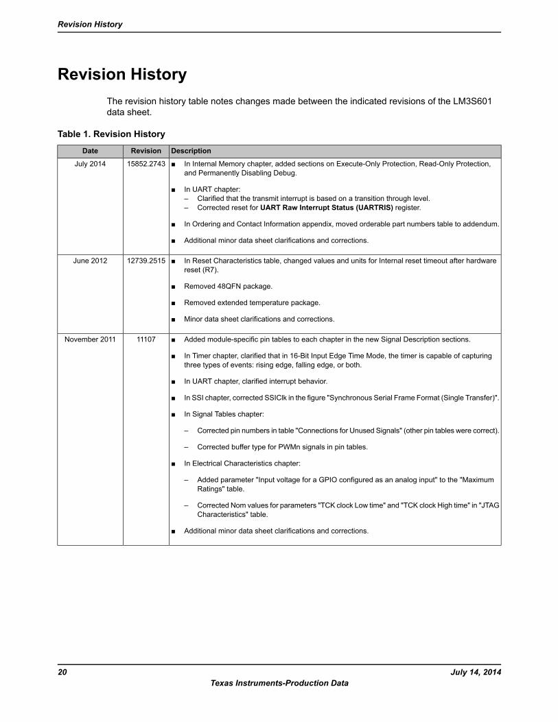
Revision HistoryThe revision history table notes changes made between the indicated revisions of the LM3S601data sheet.
Table 1. Revision History
DescriptionRevisionDate
In Internal Memory chapter, added sections on Execute-Only Protection, Read-Only Protection,and Permanently Disabling Debug.
In UART chapter:– Clarified that the transmit interrupt is based on a transition through level.– Corrected reset for UART Raw Interrupt Status (UARTRIS) register.
In Ordering and Contact Information appendix, moved orderable part numbers table to addendum.
Additional minor data sheet clarifications and corrections.
15852.2743July 2014
In Reset Characteristics table, changed values and units for Internal reset timeout after hardwarereset (R7).
Removed 48QFN package.
Removed extended temperature package.
Minor data sheet clarifications and corrections.
12739.2515June 2012
Added module-specific pin tables to each chapter in the new Signal Description sections.
In Timer chapter, clarified that in 16-Bit Input Edge Time Mode, the timer is capable of capturingthree types of events: rising edge, falling edge, or both.
In UART chapter, clarified interrupt behavior.
In SSI chapter, corrected SSIClk in the figure "Synchronous Serial Frame Format (Single Transfer)".
In Signal Tables chapter:
– Corrected pin numbers in table "Connections for Unused Signals" (other pin tables were correct).
– Corrected buffer type for PWMn signals in pin tables.
In Electrical Characteristics chapter:
– Added parameter "Input voltage for a GPIO configured as an analog input" to the "MaximumRatings" table.
– Corrected Nom values for parameters "TCK clock Low time" and "TCK clock High time" in "JTAGCharacteristics" table.
Additional minor data sheet clarifications and corrections.
11107November 2011
July 14, 201420Texas Instruments-Production Data
Revision History
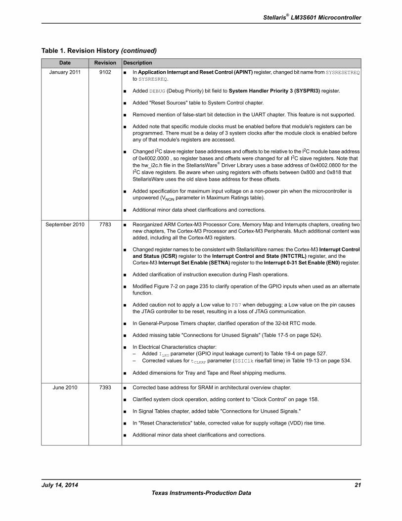
Table 1. Revision History (continued)
DescriptionRevisionDate
InApplication Interrupt andReset Control (APINT) register, changed bit name from SYSRESETREQto SYSRESREQ.
Added DEBUG (Debug Priority) bit field to System Handler Priority 3 (SYSPRI3) register.
Added "Reset Sources" table to System Control chapter.
Removed mention of false-start bit detection in the UART chapter. This feature is not supported.
Added note that specific module clocks must be enabled before that module's registers can beprogrammed. There must be a delay of 3 system clocks after the module clock is enabled beforeany of that module's registers are accessed.
Changed I2C slave register base addresses and offsets to be relative to the I2Cmodule base addressof 0x4002.0000 , so register bases and offsets were changed for all I2C slave registers. Note thatthe hw_i2c.h file in the StellarisWare® Driver Library uses a base address of 0x4002.0800 for theI2C slave registers. Be aware when using registers with offsets between 0x800 and 0x818 thatStellarisWare uses the old slave base address for these offsets.
Added specification for maximum input voltage on a non-power pin when the microcontroller isunpowered (VNON parameter in Maximum Ratings table).
Additional minor data sheet clarifications and corrections.
9102January 2011
Reorganized ARM Cortex-M3 Processor Core, Memory Map and Interrupts chapters, creating twonew chapters, The Cortex-M3 Processor and Cortex-M3 Peripherals. Much additional content wasadded, including all the Cortex-M3 registers.
Changed register names to be consistent with StellarisWare names: the Cortex-M3 Interrupt Controland Status (ICSR) register to the Interrupt Control and State (INTCTRL) register, and theCortex-M3 Interrupt Set Enable (SETNA) register to the Interrupt 0-31 Set Enable (EN0) register.
Added clarification of instruction execution during Flash operations.
Modified Figure 7-2 on page 235 to clarify operation of the GPIO inputs when used as an alternatefunction.
Added caution not to apply a Low value to PB7 when debugging; a Low value on the pin causesthe JTAG controller to be reset, resulting in a loss of JTAG communication.
In General-Purpose Timers chapter, clarified operation of the 32-bit RTC mode.
Added missing table "Connections for Unused Signals" (Table 17-5 on page 524).
In Electrical Characteristics chapter:– Added ILKG parameter (GPIO input leakage current) to Table 19-4 on page 527.– Corrected values for tCLKRF parameter (SSIClk rise/fall time) in Table 19-13 on page 534.
Added dimensions for Tray and Tape and Reel shipping mediums.
7783September 2010
Corrected base address for SRAM in architectural overview chapter.
Clarified system clock operation, adding content to “Clock Control” on page 158.
In Signal Tables chapter, added table "Connections for Unused Signals."
In "Reset Characteristics" table, corrected value for supply voltage (VDD) rise time.
Additional minor data sheet clarifications and corrections.
7393June 2010
21July 14, 2014Texas Instruments-Production Data
Stellaris® LM3S601 Microcontroller
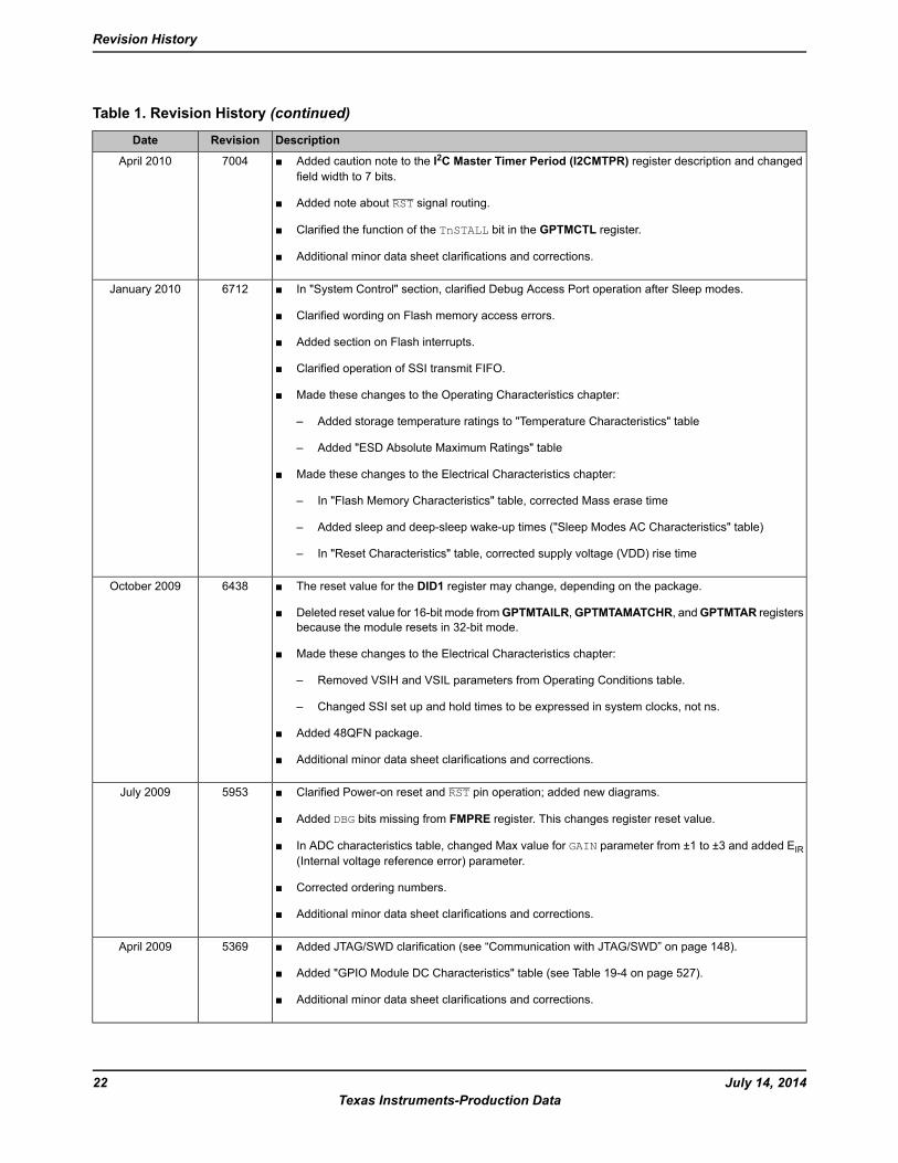
Table 1. Revision History (continued)
DescriptionRevisionDate
Added caution note to the I2C Master Timer Period (I2CMTPR) register description and changedfield width to 7 bits.
Added note about RST signal routing.
Clarified the function of the TnSTALL bit in the GPTMCTL register.
Additional minor data sheet clarifications and corrections.
7004April 2010
In "System Control" section, clarified Debug Access Port operation after Sleep modes.
Clarified wording on Flash memory access errors.
Added section on Flash interrupts.
Clarified operation of SSI transmit FIFO.
Made these changes to the Operating Characteristics chapter:
– Added storage temperature ratings to "Temperature Characteristics" table
– Added "ESD Absolute Maximum Ratings" table
Made these changes to the Electrical Characteristics chapter:
– In "Flash Memory Characteristics" table, corrected Mass erase time
– Added sleep and deep-sleep wake-up times ("Sleep Modes AC Characteristics" table)
– In "Reset Characteristics" table, corrected supply voltage (VDD) rise time
6712January 2010
The reset value for the DID1 register may change, depending on the package.
Deleted reset value for 16-bit mode fromGPTMTAILR,GPTMTAMATCHR, andGPTMTAR registersbecause the module resets in 32-bit mode.
Made these changes to the Electrical Characteristics chapter:
– Removed VSIH and VSIL parameters from Operating Conditions table.
– Changed SSI set up and hold times to be expressed in system clocks, not ns.
Added 48QFN package.
Additional minor data sheet clarifications and corrections.
6438October 2009
Clarified Power-on reset and RST pin operation; added new diagrams.
Added DBG bits missing from FMPRE register. This changes register reset value.
In ADC characteristics table, changed Max value for GAIN parameter from ±1 to ±3 and added EIR(Internal voltage reference error) parameter.
Corrected ordering numbers.
Additional minor data sheet clarifications and corrections.
5953July 2009
Added JTAG/SWD clarification (see “Communication with JTAG/SWD” on page 148).
Added "GPIO Module DC Characteristics" table (see Table 19-4 on page 527).
Additional minor data sheet clarifications and corrections.
5369April 2009
July 14, 201422Texas Instruments-Production Data
Revision History
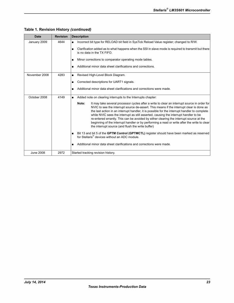
Table 1. Revision History (continued)
DescriptionRevisionDate
Incorrect bit type for RELOAD bit field in SysTick Reload Value register; changed to R/W.
Clarification added as to what happens when the SSI in slave mode is required to transmit but thereis no data in the TX FIFO.
Minor corrections to comparator operating mode tables.
Additional minor data sheet clarifications and corrections.
4644January 2009
Revised High-Level Block Diagram.
Corrected descriptions for UART1 signals.
Additional minor data sheet clarifications and corrections were made.
4283November 2008
Added note on clearing interrupts to the Interrupts chapter:
Note: It may take several processor cycles after a write to clear an interrupt source in order forNVIC to see the interrupt source de-assert. This means if the interrupt clear is done asthe last action in an interrupt handler, it is possible for the interrupt handler to completewhile NVIC sees the interrupt as still asserted, causing the interrupt handler to bere-entered errantly. This can be avoided by either clearing the interrupt source at thebeginning of the interrupt handler or by performing a read or write after the write to clearthe interrupt source (and flush the write buffer)
Bit 13 and bit 5 of the GPTM Control (GPTMCTL) register should have been marked as reservedfor Stellaris® devices without an ADC module.
Additional minor data sheet clarifications and corrections were made.
4149October 2008
Started tracking revision history.2972June 2008
23July 14, 2014Texas Instruments-Production Data
Stellaris® LM3S601 Microcontroller
About This DocumentThis data sheet provides reference information for the LM3S601 microcontroller, describing thefunctional blocks of the system-on-chip (SoC) device designed around the ARM® Cortex™-M3core.
AudienceThis manual is intended for system software developers, hardware designers, and applicationdevelopers.
About This ManualThis document is organized into sections that correspond to each major feature.
Related DocumentsThe following related documents are available on the Stellaris® web site at www.ti.com/stellaris:
Stellaris® Errata
ARM® Cortex™-M3 Errata
Cortex™-M3/M4 Instruction Set Technical User's Manual
Stellaris® Graphics Library User's Guide
Stellaris® Peripheral Driver Library User's Guide
The following related documents are also referenced:
ARM® Debug Interface V5 Architecture Specification
ARM® Embedded Trace Macrocell Architecture Specification
IEEE Standard 1149.1-Test Access Port and Boundary-Scan Architecture
This documentation list was current as of publication date. Please check the web site for additionaldocumentation, including application notes and white papers.
July 14, 201424Texas Instruments-Production Data
About This Document
Documentation ConventionsThis document uses the conventions shown in Table 2 on page 25.
Table 2. Documentation Conventions
MeaningNotation
General Register Notation
APB registers are indicated in uppercase bold. For example, PBORCTL is the Power-On andBrown-Out Reset Control register. If a register name contains a lowercase n, it represents morethan one register. For example, SRCRn represents any (or all) of the three Software Reset Controlregisters: SRCR0, SRCR1 , and SRCR2.
REGISTER
A single bit in a register.bit
Two or more consecutive and related bits.bit field
A hexadecimal increment to a register's address, relative to that module's base address as specifiedin Table 2-4 on page 62.
offset 0xnnn
Registers are numbered consecutively throughout the document to aid in referencing them. Theregister number has no meaning to software.
Register N
Register bits marked reserved are reserved for future use. In most cases, reserved bits are set to0; however, user software should not rely on the value of a reserved bit. To provide softwarecompatibility with future products, the value of a reserved bit should be preserved across aread-modify-write operation.
reserved
The range of register bits inclusive from xx to yy. For example, 31:15 means bits 15 through 31 inthat register.
yy:xx
This value in the register bit diagram indicates whether software running on the controller canchange the value of the bit field.
Register Bit/FieldTypes
Software can read this field. The bit or field is cleared by hardware after reading the bit/field.RC
Software can read this field. Always write the chip reset value.RO
Software can read or write this field.R/W
Software can read or write this field. Writing to it with any value clears the register.R/WC
Software can read or write this field. A write of a 0 to a W1C bit does not affect the bit value in theregister. A write of a 1 clears the value of the bit in the register; the remaining bits remain unchanged.This register type is primarily used for clearing interrupt status bits where the read operationprovides the interrupt status and the write of the read value clears only the interrupts being reportedat the time the register was read.
R/W1C
Software can read or write a 1 to this field. A write of a 0 to a R/W1S bit does not affect the bitvalue in the register.
R/W1S
Software can write this field. A write of a 0 to a W1C bit does not affect the bit value in the register.A write of a 1 clears the value of the bit in the register; the remaining bits remain unchanged. Aread of the register returns no meaningful data.This register is typically used to clear the corresponding bit in an interrupt register.
W1C
Only a write by software is valid; a read of the register returns no meaningful data.WO
This value in the register bit diagram shows the bit/field value after any reset, unless noted.Register Bit/FieldReset Value
Bit cleared to 0 on chip reset.0
Bit set to 1 on chip reset.1
Nondeterministic.-
Pin/Signal Notation
Pin alternate function; a pin defaults to the signal without the brackets.[ ]
Refers to the physical connection on the package.pin
Refers to the electrical signal encoding of a pin.signal
25July 14, 2014Texas Instruments-Production Data
Stellaris® LM3S601 Microcontroller
Table 2. Documentation Conventions (continued)
MeaningNotation
Change the value of the signal from the logically False state to the logically True state. For activeHigh signals, the asserted signal value is 1 (High); for active Low signals, the asserted signal valueis 0 (Low). The active polarity (High or Low) is defined by the signal name (see SIGNAL and SIGNALbelow).
assert a signal
Change the value of the signal from the logically True state to the logically False state.deassert a signal
Signal names are in uppercase and in the Courier font. An overbar on a signal name indicates thatit is active Low. To assert SIGNAL is to drive it Low; to deassert SIGNAL is to drive it High.
SIGNAL
Signal names are in uppercase and in the Courier font. An active High signal has no overbar. Toassert SIGNAL is to drive it High; to deassert SIGNAL is to drive it Low.
SIGNAL
Numbers
An uppercase X indicates any of several values is allowed, where X can be any legal pattern. Forexample, a binary value of 0X00 can be either 0100 or 0000, a hex value of 0xX is 0x0 or 0x1, andso on.
X
Hexadecimal numbers have a prefix of 0x. For example, 0x00FF is the hexadecimal number FF.All other numbers within register tables are assumed to be binary. Within conceptual information,binary numbers are indicated with a b suffix, for example, 1011b, and decimal numbers are writtenwithout a prefix or suffix.
0x
July 14, 201426Texas Instruments-Production Data
About This Document
1 Architectural OverviewThe Stellaris® family of microcontrollers—the first ARM® Cortex™-M3 based controllers—bringshigh-performance 32-bit computing to cost-sensitive embedded microcontroller applications. Thesepioneering parts deliver customers 32-bit performance at a cost equivalent to legacy 8- and 16-bitdevices, all in a package with a small footprint.
The LM3S601 microcontroller is targeted for industrial applications, including test and measurementequipment, factory automation, HVAC and building control, motion control, medical instrumentation,fire and security, and power/energy.
In addition, the LM3S601 microcontroller offers the advantages of ARM's widely availabledevelopment tools, System-on-Chip (SoC) infrastructure IP applications, and a large user community.Additionally, the microcontroller uses ARM's Thumb®-compatible Thumb-2 instruction set to reducememory requirements and, thereby, cost. Finally, the LM3S601 microcontroller is code-compatibleto all members of the extensive Stellaris family; providing flexibility to fit our customers' preciseneeds.
Texas Instruments offers a complete solution to get to market quickly, with evaluation anddevelopment boards, white papers and application notes, an easy-to-use peripheral driver library,and a strong support, sales, and distributor network. See “Ordering and ContactInformation” on page 561 for ordering information for Stellaris family devices.
1.1 Product FeaturesThe LM3S601 microcontroller includes the following product features:
32-Bit RISC Performance
– 32-bit ARM® Cortex™-M3 v7M architecture optimized for small-footprint embeddedapplications
– System timer (SysTick), providing a simple, 24-bit clear-on-write, decrementing, wrap-on-zerocounter with a flexible control mechanism
– Thumb®-compatible Thumb-2-only instruction set processor core for high code density
– 50-MHz operation
– Hardware-division and single-cycle-multiplication
– Integrated Nested Vectored Interrupt Controller (NVIC) providing deterministic interrupthandling
– 25 interrupts with eight priority levels
– Memory protection unit (MPU), providing a privileged mode for protected operating systemfunctionality
– Unaligned data access, enabling data to be efficiently packed into memory
– Atomic bit manipulation (bit-banding), delivering maximummemory utilization and streamlinedperipheral control
ARM® Cortex™-M3 Processor Core
27July 14, 2014Texas Instruments-Production Data
Stellaris® LM3S601 Microcontroller
– Compact core.
– Thumb-2 instruction set, delivering the high-performance expected of an ARM core in thememory size usually associated with 8- and 16-bit devices; typically in the range of a fewkilobytes of memory for microcontroller class applications.
– Rapid application execution through Harvard architecture characterized by separate busesfor instruction and data.
– Exceptional interrupt handling, by implementing the register manipulations required for handlingan interrupt in hardware.
– Deterministic, fast interrupt processing: always 12 cycles, or just 6 cycles with tail-chaining
– Memory protection unit (MPU) to provide a privileged mode of operation for complexapplications.
– Migration from the ARM7™ processor family for better performance and power efficiency.
– Full-featured debug solution
• Serial Wire JTAG Debug Port (SWJ-DP)
• Flash Patch and Breakpoint (FPB) unit for implementing breakpoints
• Data Watchpoint and Trigger (DWT) unit for implementing watchpoints, trigger resources,and system profiling
• Instrumentation Trace Macrocell (ITM) for support of printf style debugging
• Trace Port Interface Unit (TPIU) for bridging to a Trace Port Analyzer
– Optimized for single-cycle flash usage
– Three sleep modes with clock gating for low power
– Single-cycle multiply instruction and hardware divide
– Atomic operations
– ARM Thumb2 mixed 16-/32-bit instruction set
– 1.25 DMIPS/MHz
JTAG
– IEEE 1149.1-1990 compatible Test Access Port (TAP) controller
– Four-bit Instruction Register (IR) chain for storing JTAG instructions
– IEEE standard instructions: BYPASS, IDCODE, SAMPLE/PRELOAD, EXTEST and INTEST
– ARM additional instructions: APACC, DPACC and ABORT
– Integrated ARM Serial Wire Debug (SWD)
July 14, 201428Texas Instruments-Production Data
Architectural Overview
Internal Memory
– 32 KB single-cycle flash
• User-managed flash block protection on a 2-KB block basis
• User-managed flash data programming
• User-defined and managed flash-protection block
– 8 KB single-cycle SRAM
GPIOs
– 0-36 GPIOs, depending on configuration
– 5-V-tolerant in input configuration
– Fast toggle capable of a change every two clock cycles
– Programmable control for GPIO interrupts
• Interrupt generation masking
• Edge-triggered on rising, falling, or both
• Level-sensitive on High or Low values
– Bit masking in both read and write operations through address lines
– Pins configured as digital inputs are Schmitt-triggered.
– Programmable control for GPIO pad configuration
• Weak pull-up or pull-down resistors
• 2-mA, 4-mA, and 8-mA pad drive for digital communication
• Slew rate control for the 8-mA drive
• Open drain enables
• Digital input enables
General-Purpose Timers
– Three General-Purpose Timer Modules (GPTM), each of which provides two 16-bittimers/counters. Each GPTM can be configured to operate independently:
• As a single 32-bit timer
• As one 32-bit Real-Time Clock (RTC) to event capture
• For Pulse Width Modulation (PWM)
– 32-bit Timer modes
29July 14, 2014Texas Instruments-Production Data
Stellaris® LM3S601 Microcontroller
Programmable one-shot timer•
• Programmable periodic timer
• Real-Time Clock when using an external 32.768-KHz clock as the input
• User-enabled stalling when the controller asserts CPU Halt flag during debug
– 16-bit Timer modes
• General-purpose timer function with an 8-bit prescaler (for one-shot and periodic modesonly)
• Programmable one-shot timer
• Programmable periodic timer
• User-enabled stalling when the controller asserts CPU Halt flag during debug
– 16-bit Input Capture modes
• Input edge count capture
• Input edge time capture
– 16-bit PWM mode
• Simple PWM mode with software-programmable output inversion of the PWM signal
ARM FiRM-compliant Watchdog Timer
– 32-bit down counter with a programmable load register
– Separate watchdog clock with an enable
– Programmable interrupt generation logic with interrupt masking
– Lock register protection from runaway software
– Reset generation logic with an enable/disable
– User-enabled stalling when the controller asserts the CPU Halt flag during debug
UART
– Two fully programmable 16C550-type UARTs
– Separate 16x8 transmit (TX) and receive (RX) FIFOs to reduce CPU interrupt service loading
– Programmable baud-rate generator allowing speeds up to 3.125 Mbps
– Programmable FIFO length, including 1-byte deep operation providing conventionaldouble-buffered interface
– FIFO trigger levels of 1/8, 1/4, 1/2, 3/4, and 7/8
– Standard asynchronous communication bits for start, stop, and parity
July 14, 201430Texas Instruments-Production Data
Architectural Overview
– Line-break generation and detection
– Fully programmable serial interface characteristics
• 5, 6, 7, or 8 data bits
• Even, odd, stick, or no-parity bit generation/detection
• 1 or 2 stop bit generation
Synchronous Serial Interface (SSI)
– Master or slave operation
– Programmable clock bit rate and prescale
– Separate transmit and receive FIFOs, 16 bits wide, 8 locations deep
– Programmable interface operation for Freescale SPI, MICROWIRE, or Texas Instrumentssynchronous serial interfaces
– Programmable data frame size from 4 to 16 bits
– Internal loopback test mode for diagnostic/debug testing
I2C
– Devices on the I2C bus can be designated as either a master or a slave
• Supports both sending and receiving data as either a master or a slave
• Supports simultaneous master and slave operation
– Four I2C modes
• Master transmit
• Master receive
• Slave transmit
• Slave receive
– Two transmission speeds: Standard (100 Kbps) and Fast (400 Kbps)
– Master and slave interrupt generation
• Master generates interrupts when a transmit or receive operation completes (or abortsdue to an error)
• Slave generates interrupts when data has been sent or requested by a master
– Master with arbitration and clock synchronization, multimaster support, and 7-bit addressingmode
Analog Comparators
31July 14, 2014Texas Instruments-Production Data
Stellaris® LM3S601 Microcontroller
– Three independent integrated analog comparators
– Configurable for output to drive an output pin or generate an interrupt
– Compare external pin input to external pin input or to internal programmable voltage reference
– Compare a test voltage against any one of these voltages
• An individual external reference voltage
• A shared single external reference voltage
• A shared internal reference voltage
PWM
– Three PWM generator blocks, each with one 16-bit counter, two PWM comparators, a PWMsignal generator, a dead-band generator, and an interrupt selector
– One fault input in hardware to promote low-latency shutdown
– One 16-bit counter
• Runs in Down or Up/Down mode
• Output frequency controlled by a 16-bit load value
• Load value updates can be synchronized
• Produces output signals at zero and load value
– Two PWM comparators
• Comparator value updates can be synchronized
• Produces output signals on match
– PWM generator
• Output PWM signal is constructed based on actions taken as a result of the counter andPWM comparator output signals
• Produces two independent PWM signals
– Dead-band generator
• Produces two PWM signals with programmable dead-band delays suitable for driving ahalf-H bridge
• Can be bypassed, leaving input PWM signals unmodified
– Flexible output control block with PWM output enable of each PWM signal
• PWM output enable of each PWM signal
• Optional output inversion of each PWM signal (polarity control)
July 14, 201432Texas Instruments-Production Data
Architectural Overview
• Optional fault handling for each PWM signal
• Synchronization of timers in the PWM generator blocks
• Interrupt status summary of the PWM generator blocks
QEI
– Position integrator that tracks the encoder position
– Velocity capture using built-in timer
– The input frequency of the QEI inputs may be as high as 1/4 of the processor frequency (forexample, 12.5 MHz for a 50-MHz system)
– Interrupt generation on:
• Index pulse
• Velocity-timer expiration
• Direction change
• Quadrature error detection
Power
– On-chip Low Drop-Out (LDO) voltage regulator, with programmable output user-adjustablefrom 2.25 V to 2.75 V
– Low-power options on controller: Sleep and Deep-sleep modes
– Low-power options for peripherals: software controls shutdown of individual peripherals
– User-enabled LDO unregulated voltage detection and automatic reset
– 3.3-V supply brown-out detection and reporting via interrupt or reset
Flexible Reset Sources
– Power-on reset (POR)
– Reset pin assertion
– Brown-out (BOR) detector alerts to system power drops
– Software reset
– Watchdog timer reset
– Internal low drop-out (LDO) regulator output goes unregulated
Industrial temperature 48-pin RoHS-compliant LQFP package
33July 14, 2014Texas Instruments-Production Data
Stellaris® LM3S601 Microcontroller
1.2 Target Applications Factory automation and control
Industrial control power devices
Building and home automation
Stepper motors
Brushless DC motors
AC induction motors
1.3 High-Level Block DiagramFigure 1-1 on page 35 depicts the features on the Stellaris LM3S601 microcontroller.
July 14, 201434Texas Instruments-Production Data
Architectural Overview
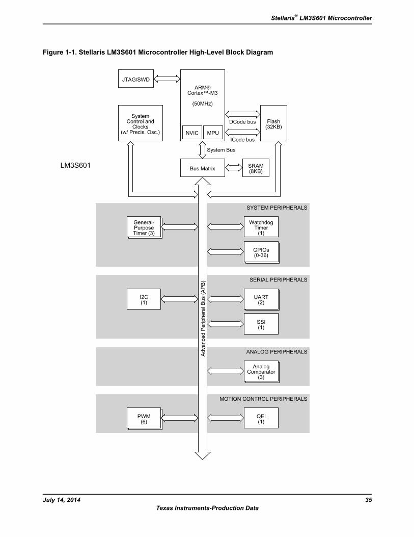
Figure 1-1. Stellaris LM3S601 Microcontroller High-Level Block Diagram
ARM®Cortex™-M3
(50MHz)
NVIC MPU
Flash(32KB)
DCode bus
ICode bus
JTAG/SWD
SystemControl andClocks
(w/ Precis. Osc.)
Bus Matrix
System Bus
SRAM(8KB)
SYSTEM PERIPHERALS
WatchdogTimer(1)
General-PurposeTimer (3)
GPIOs(0-36)
SERIAL PERIPHERALS
UART(2)
I2C(1)
SSI(1)
ANALOG PERIPHERALS
AnalogComparator
(3)
MOTION CONTROL PERIPHERALS
QEI(1)
PWM(6)
Advanced
PeripheralB
us(APB
)
LM3S601
35July 14, 2014Texas Instruments-Production Data
Stellaris® LM3S601 Microcontroller
1.4 Functional OverviewThe following sections provide an overview of the features of the LM3S601 microcontroller. Thepage number in parenthesis indicates where that feature is discussed in detail. Ordering and supportinformation can be found in “Ordering and Contact Information” on page 561.
1.4.1 ARM Cortex™-M3
1.4.1.1 Processor Core (see page 43)All members of the Stellaris product family, including the LM3S601 microcontroller, are designedaround an ARM Cortex™-M3 processor core. The ARM Cortex-M3 processor provides the core fora high-performance, low-cost platform that meets the needs of minimal memory implementation,reduced pin count, and low-power consumption, while delivering outstanding computationalperformance and exceptional system response to interrupts.
1.4.1.2 Memory Map (see page 62)A memory map lists the location of instructions and data in memory. The memory map for theLM3S601 controller can be found in Table 2-4 on page 62. Register addresses are given as ahexadecimal increment, relative to the module's base address as shown in the memory map.
1.4.1.3 System Timer (SysTick) (see page 85)Cortex-M3 includes an integrated system timer, SysTick. SysTick provides a simple, 24-bitclear-on-write, decrementing, wrap-on-zero counter with a flexible control mechanism. The countercan be used in several different ways, for example:
An RTOS tick timer which fires at a programmable rate (for example, 100 Hz) and invokes aSysTick routine.
A high-speed alarm timer using the system clock.
A variable rate alarm or signal timer—the duration is range-dependent on the reference clockused and the dynamic range of the counter.
A simple counter. Software can use this to measure time to completion and time used.
An internal clock source control based on missing/meeting durations. The COUNTFLAG bit-fieldin the control and status register can be used to determine if an action completed within a setduration, as part of a dynamic clock management control loop.
1.4.1.4 Nested Vectored Interrupt Controller (NVIC) (see page 86)The LM3S601 controller includes the ARM Nested Vectored Interrupt Controller (NVIC) on theARM®Cortex™-M3 core. The NVIC and Cortex-M3 prioritize and handle all exceptions. All exceptionsare handled in Handler Mode. The processor state is automatically stored to the stack on anexception, and automatically restored from the stack at the end of the Interrupt Service Routine(ISR). The vector is fetched in parallel to the state saving, which enables efficient interrupt entry.The processor supports tail-chaining, which enables back-to-back interrupts to be performed withoutthe overhead of state saving and restoration. Software can set eight priority levels on 7 exceptions(system handlers) and 25 interrupts.
July 14, 201436Texas Instruments-Production Data
Architectural Overview
1.4.1.5 System Control Block (SCB) (see page 88)The SCB provides system implementation information and system control, including configuration,control, and reporting of system exceptions.
1.4.1.6 Memory Protection Unit (MPU) (see page 88)The MPU supports the standard ARMv7 Protected Memory System Architecture (PMSA) model.The MPU provides full support for protection regions, overlapping protection regions, accesspermissions, and exporting memory attributes to the system.
1.4.2 Motor Control PeripheralsTo enhance motor control, the LM3S601 controller features Pulse Width Modulation (PWM) outputsand the Quadrature Encoder Interface (QEI).
1.4.2.1 PWMPulse width modulation (PWM) is a powerful technique for digitally encoding analog signal levels.High-resolution counters are used to generate a square wave, and the duty cycle of the squarewave is modulated to encode an analog signal. Typical applications include switching power suppliesand motor control.
On the LM3S601, PWM motion control functionality can be achieved through:
Dedicated, flexible motion control hardware using the PWM pins
The motion control features of the general-purpose timers using the CCP pins
PWM Pins (see page 460)
The LM3S601 PWM module consists of three PWM generator blocks and a control block. EachPWM generator block contains one timer (16-bit down or up/down counter), two comparators, aPWM signal generator, a dead-band generator, and an interrupt. The control block determines thepolarity of the PWM signals, and which signals are passed through to the pins.
Each PWM generator block produces two PWM signals that can either be independent signals ora single pair of complementary signals with dead-band delays inserted. The output of the PWMgeneration blocks are managed by the output control block before being passed to the device pins.
CCP Pins (see page 278)
TheGeneral-Purpose TimerModule's CCP (Capture Compare PWM) pins are software programmableto support a simple PWMmode with a software-programmable output inversion of the PWM signal.
Fault Pin (see page 466)
The LM3S601 PWMmodule includes one fault-condition handling input to quickly provide low-latencyshutdown and prevent damage to the motor being controlled.
1.4.2.2 QEI (see page 498)A quadrature encoder, also known as a 2-channel incremental encoder, converts linear displacementinto a pulse signal. By monitoring both the number of pulses and the relative phase of the two signals,you can track the position, direction of rotation, and speed. In addition, a third channel, or indexsignal, can be used to reset the position counter.
37July 14, 2014Texas Instruments-Production Data
Stellaris® LM3S601 Microcontroller
The Stellaris quadrature encoder with index (QEI) module interprets the code produced by aquadrature encoder wheel to integrate position over time and determine direction of rotation. Inaddition, it can capture a running estimate of the velocity of the encoder wheel.
1.4.3 Analog PeripheralsFor support of analog signals, the LM3S601 microcontroller offers three analog comparators.
1.4.3.1 Analog Comparators (see page 447)An analog comparator is a peripheral that compares two analog voltages, and provides a logicaloutput that signals the comparison result.
The LM3S601 microcontroller provides three independent integrated analog comparators that canbe configured to drive an output or generate an interrupt .
A comparator can compare a test voltage against any one of these voltages:
An individual external reference voltage
A shared single external reference voltage
A shared internal reference voltage
The comparator can provide its output to a device pin, acting as a replacement for an analogcomparator on the board, or it can be used to signal the application via interrupts to cause it to startcapturing a sample sequence.
1.4.4 Serial Communications PeripheralsThe LM3S601 controller supports both asynchronous and synchronous serial communications with:
Two fully programmable 16C550-type UARTs
One SSI module
One I2C module
1.4.4.1 UART (see page 332)A Universal Asynchronous Receiver/Transmitter (UART) is an integrated circuit used for RS-232Cserial communications, containing a transmitter (parallel-to-serial converter) and a receiver(serial-to-parallel converter), each clocked separately.
The LM3S601 controller includes two fully programmable 16C550-type UARTs that support datatransfer speeds up to 3.125 Mbps. (Although similar in functionality to a 16C550 UART, it is notregister-compatible.)
Separate 16x8 transmit (TX) and receive (RX) FIFOs reduce CPU interrupt service loading. TheUART can generate individually masked interrupts from the RX, TX, modem status, and errorconditions. The module provides a single combined interrupt when any of the interrupts are assertedand are unmasked.
1.4.4.2 SSI (see page 372)Synchronous Serial Interface (SSI) is a four-wire bi-directional full and low-speed communicationsinterface.
July 14, 201438Texas Instruments-Production Data
Architectural Overview
The LM3S601 controller includes one SSI module that provides the functionality for synchronousserial communications with peripheral devices, and can be configured to use the Freescale SPI,MICROWIRE, or TI synchronous serial interface frame formats. The size of the data frame is alsoconfigurable, and can be set between 4 and 16 bits, inclusive.
The SSI module performs serial-to-parallel conversion on data received from a peripheral device,and parallel-to-serial conversion on data transmitted to a peripheral device. The TX and RX pathsare buffered with internal FIFOs, allowing up to eight 16-bit values to be stored independently.
The SSI module can be configured as either a master or slave device. As a slave device, the SSImodule can also be configured to disable its output, which allows a master device to be coupledwith multiple slave devices.
The SSI module also includes a programmable bit rate clock divider and prescaler to generate theoutput serial clock derived from the SSI module's input clock. Bit rates are generated based on theinput clock and the maximum bit rate is determined by the connected peripheral.
1.4.4.3 I2C (see page 410)The Inter-Integrated Circuit (I2C) bus provides bi-directional data transfer through a two-wire design(a serial data line SDA and a serial clock line SCL).
The I2C bus interfaces to external I2C devices such as serial memory (RAMs and ROMs), networkingdevices, LCDs, tone generators, and so on. The I2C bus may also be used for system testing anddiagnostic purposes in product development and manufacture.
The LM3S601 controller includes one I2C module that provides the ability to communicate to otherIC devices over an I2C bus. The I2C bus supports devices that can both transmit and receive (writeand read) data.
Devices on the I2C bus can be designated as either a master or a slave. The I2C module supportsboth sending and receiving data as either a master or a slave, and also supports the simultaneousoperation as both a master and a slave. The four I2C modes are: Master Transmit, Master Receive,Slave Transmit, and Slave Receive.
A Stellaris I2C module can operate at two speeds: Standard (100 Kbps) and Fast (400 Kbps).
Both the I2C master and slave can generate interrupts. The I2C master generates interrupts whena transmit or receive operation completes (or aborts due to an error). The I2C slave generatesinterrupts when data has been sent or requested by a master.
1.4.5 System Peripherals
1.4.5.1 Programmable GPIOs (see page 230)General-purpose input/output (GPIO) pins offer flexibility for a variety of connections.
The Stellaris GPIO module is comprised of five physical GPIO blocks, each corresponding to anindividual GPIO port. The GPIO module is FiRM-compliant (compliant to the ARM Foundation IPfor Real-Time Microcontrollers specification) and supports 0-36 programmable input/output pins.The number of GPIOs available depends on the peripherals being used (see “SignalTables” on page 517 for the signals available to each GPIO pin).
The GPIO module features programmable interrupt generation as either edge-triggered orlevel-sensitive on all pins, programmable control for GPIO pad configuration, and bit masking inboth read and write operations through address lines. Pins configured as digital inputs areSchmitt-triggered.
39July 14, 2014Texas Instruments-Production Data
Stellaris® LM3S601 Microcontroller
1.4.5.2 Three Programmable Timers (see page 272)Programmable timers can be used to count or time external events that drive the Timer input pins.
The Stellaris General-Purpose Timer Module (GPTM) contains three GPTM blocks. Each GPTMblock provides two 16-bit timers/counters that can be configured to operate independently as timersor event counters, or configured to operate as one 32-bit timer or one 32-bit Real-Time Clock (RTC).
When configured in 32-bit mode, a timer can run as a Real-Time Clock (RTC), one-shot timer orperiodic timer. When in 16-bit mode, a timer can run as a one-shot timer or periodic timer, and canextend its precision by using an 8-bit prescaler. A 16-bit timer can also be configured for eventcapture or Pulse Width Modulation (PWM) generation.
1.4.5.3 Watchdog Timer (see page 308)A watchdog timer can generate an interrupt or a reset when a time-out value is reached. Thewatchdog timer is used to regain control when a system has failed due to a software error or to thefailure of an external device to respond in the expected way.
The Stellaris Watchdog Timer module consists of a 32-bit down counter, a programmable loadregister, interrupt generation logic, and a locking register.
The Watchdog Timer can be configured to generate an interrupt to the controller on its first time-out,and to generate a reset signal on its second time-out. Once theWatchdog Timer has been configured,the lock register can be written to prevent the timer configuration from being inadvertently altered.
1.4.6 Memory PeripheralsThe LM3S601 controller offers both single-cycle SRAM and single-cycle Flash memory.
1.4.6.1 SRAM (see page 212)The LM3S601 static random access memory (SRAM) controller supports 8 KB SRAM. The internalSRAM of the Stellaris devices starts at base address 0x2000.0000 of the device memory map. Toreduce the number of time-consuming read-modify-write (RMW) operations, ARM has introducedbit-banding technology in the new Cortex-M3 processor. With a bit-band-enabled processor, certainregions in the memory map (SRAM and peripheral space) can use address aliases to accessindividual bits in a single, atomic operation.
1.4.6.2 Flash (see page 213)The LM3S601 Flash controller supports 32 KB of flash memory. The flash is organized as a set of1-KB blocks that can be individually erased. Erasing a block causes the entire contents of the blockto be reset to all 1s. These blocks are paired into a set of 2-KB blocks that can be individuallyprotected. The blocks can be marked as read-only or execute-only, providing different levels of codeprotection. Read-only blocks cannot be erased or programmed, protecting the contents of thoseblocks from being modified. Execute-only blocks cannot be erased or programmed, and can onlybe read by the controller instruction fetch mechanism, protecting the contents of those blocks frombeing read by either the controller or by a debugger.
1.4.7 Additional Features
1.4.7.1 JTAG TAP Controller (see page 143)The Joint Test Action Group (JTAG) port is an IEEE standard that defines a Test Access Port andBoundary Scan Architecture for digital integrated circuits and provides a standardized serial interfacefor controlling the associated test logic. The TAP, Instruction Register (IR), and Data Registers (DR)can be used to test the interconnections of assembled printed circuit boards and obtain manufacturing
July 14, 201440Texas Instruments-Production Data
Architectural Overview
information on the components. The JTAG Port also provides a means of accessing and controllingdesign-for-test features such as I/O pin observation and control, scan testing, and debugging.
The JTAG port is composed of the standard five pins: TRST, TCK, TMS, TDI, and TDO. Data istransmitted serially into the controller on TDI and out of the controller on TDO. The interpretation ofthis data is dependent on the current state of the TAP controller. For detailed information on theoperation of the JTAG port and TAP controller, please refer to the IEEE Standard 1149.1-TestAccess Port and Boundary-Scan Architecture.
The Stellaris JTAG controller works with the ARM JTAG controller built into the Cortex-M3 core.This is implemented by multiplexing the TDO outputs from both JTAG controllers. ARM JTAGinstructions select the ARM TDO output while Stellaris JTAG instructions select the Stellaris TDOoutputs. The multiplexer is controlled by the Stellaris JTAG controller, which has comprehensiveprogramming for the ARM, Stellaris, and unimplemented JTAG instructions.
1.4.7.2 System Control and Clocks (see page 153)System control determines the overall operation of the device. It provides information about thedevice, controls the clocking of the device and individual peripherals, and handles reset detectionand reporting.
1.4.8 Hardware DetailsDetails on the pins and package can be found in the following sections:
“Pin Diagram” on page 516
“Signal Tables” on page 517
“Operating Characteristics” on page 525
“Electrical Characteristics” on page 526
“Package Information” on page 563
41July 14, 2014Texas Instruments-Production Data
Stellaris® LM3S601 Microcontroller
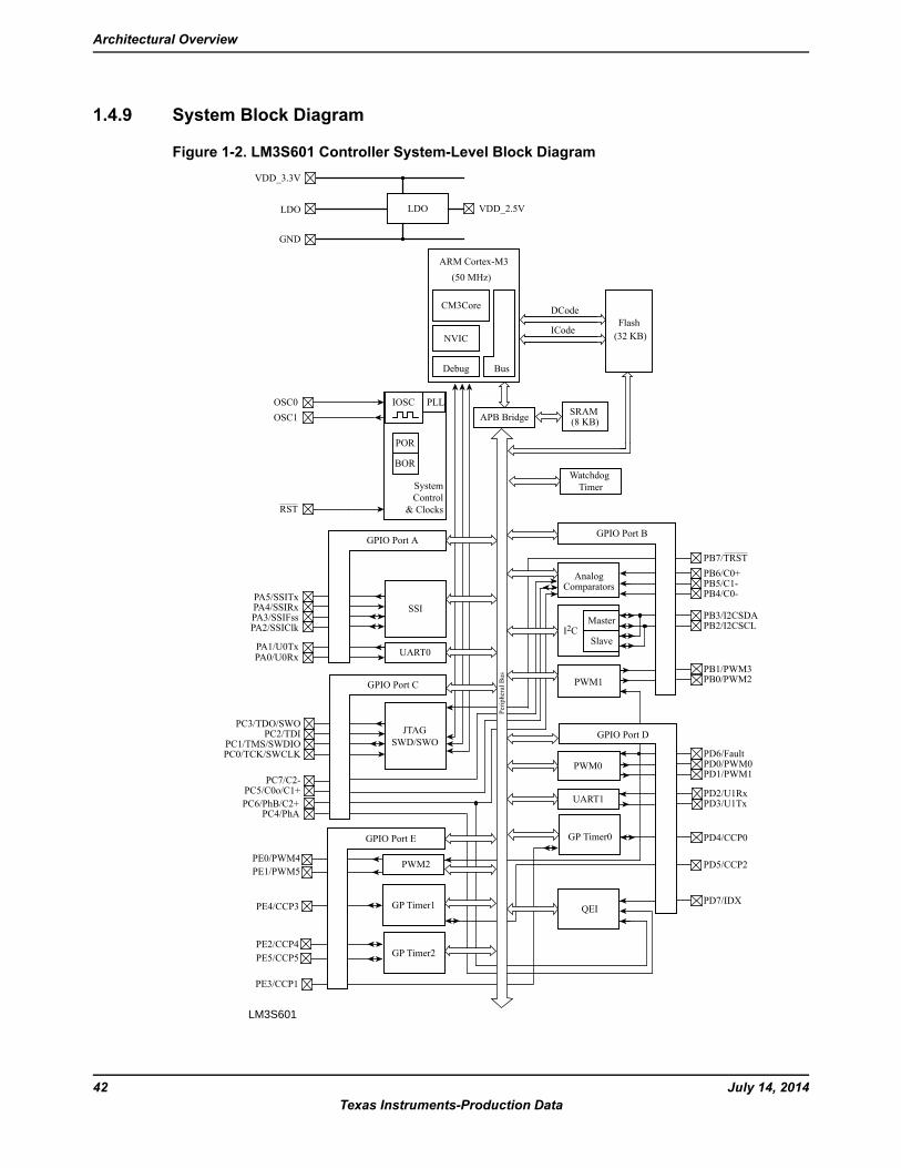
1.4.9 System Block Diagram
Figure 1-2. LM3S601 Controller System-Level Block Diagram
Flash
SRAMAPB Bridge
ICode
DCode
GND
VDD_3.3V
LDO VDD_2.5VLDO
SystemControl
& Clocks
OSC0OSC1
RST
PLL
WatchdogTimer
POR
BOR
IOSC
Debug
ARM Cortex-M3
NVIC
CM3Core
Bus
UART0
GPIO Port A
SSI
(8 KB)
(32 KB)
(50 MHz)
GPIO Port B
GPIO Port C
PB3/I2CSDAPB2/I2CSCL
PB5/C1-PB4/C0-
PB6/C0+PB7/TRST
AnalogComparators
GPIO Port E
PE0/PWM4PE1/PWM5
PWM0 PD0/PWM0PD1/PWM1
PD7/IDX
PD4/CCP0
PD6/Fault
PD5/CCP2
UART1 PD2/U1RxPD3/U1Tx
PWM1PB1/PWM3PB0/PWM2
PC5/C0o/C1+PC6/PhB/C2+
PE3/CCP1
PC4/PhA
PWM2
GP Timer1
GP Timer2
PE4/CCP3
PE2/CCP4PE5/CCP5
PC7/C2-
GP Timer0
LM3S601
Perip
heralB
us
JTAGSWD/SWOPC1/TMS/SWDIO
PC0/TCK/SWCLK
PC3/TDO/SWO
PA0/U0Rx
PA3/SSIFssPA2/SSIClk
PA5/SSITxPA4/SSIRx
PA1/U0Tx
PC2/TDI
I2CMaster
Slave
QEI
Perip
heralB
us
GPIO Port D
July 14, 201442Texas Instruments-Production Data
Architectural Overview
2 The Cortex-M3 ProcessorThe ARM® Cortex™-M3 processor provides a high-performance, low-cost platform that meets thesystem requirements of minimal memory implementation, reduced pin count, and low powerconsumption, while delivering outstanding computational performance and exceptional systemresponse to interrupts. Features include:
Compact core.
Thumb-2 instruction set, delivering the high-performance expected of an ARM core in the memorysize usually associated with 8- and 16-bit devices; typically in the range of a few kilobytes ofmemory for microcontroller class applications.
Rapid application execution through Harvard architecture characterized by separate buses forinstruction and data.
Exceptional interrupt handling, by implementing the register manipulations required for handlingan interrupt in hardware.
Deterministic, fast interrupt processing: always 12 cycles, or just 6 cycles with tail-chaining
Memory protection unit (MPU) to provide a privileged mode of operation for complex applications.
Migration from the ARM7™ processor family for better performance and power efficiency.
Full-featured debug solution
– Serial Wire JTAG Debug Port (SWJ-DP)
– Flash Patch and Breakpoint (FPB) unit for implementing breakpoints
– Data Watchpoint and Trigger (DWT) unit for implementing watchpoints, trigger resources,and system profiling
– Instrumentation Trace Macrocell (ITM) for support of printf style debugging
– Trace Port Interface Unit (TPIU) for bridging to a Trace Port Analyzer
Optimized for single-cycle flash usage
Three sleep modes with clock gating for low power
Single-cycle multiply instruction and hardware divide
Atomic operations
ARM Thumb2 mixed 16-/32-bit instruction set
1.25 DMIPS/MHz
The Stellaris® family of microcontrollers builds on this core to bring high-performance 32-bit computingto cost-sensitive embedded microcontroller applications, such as factory automation and control,industrial control power devices, building and home automation, and stepper motor control.
43July 14, 2014Texas Instruments-Production Data
Stellaris® LM3S601 Microcontroller
This chapter provides information on the Stellaris implementation of the Cortex-M3 processor,including the programming model, the memory model, the exception model, fault handling, andpower management.
For technical details on the instruction set, see theCortex™-M3/M4 Instruction Set Technical User'sManual.
2.1 Block DiagramThe Cortex-M3 processor is built on a high-performance processor core, with a 3-stage pipelineHarvard architecture, making it ideal for demanding embedded applications. The processor deliversexceptional power efficiency through an efficient instruction set and extensively optimized design,providing high-end processing hardware including a range of single-cycle and SIMD multiplicationand multiply-with-accumulate capabilities, saturating arithmetic and dedicated hardware division.
To facilitate the design of cost-sensitive devices, the Cortex-M3 processor implements tightly coupledsystem components that reduce processor area while significantly improving interrupt handling andsystem debug capabilities. The Cortex-M3 processor implements a version of the Thumb® instructionset based on Thumb-2 technology, ensuring high code density and reduced program memoryrequirements. The Cortex-M3 instruction set provides the exceptional performance expected of amodern 32-bit architecture, with the high code density of 8-bit and 16-bit microcontrollers.
The Cortex-M3 processor closely integrates a nested interrupt controller (NVIC), to deliverindustry-leading interrupt performance. The Stellaris NVIC includes a non-maskable interrupt (NMI)and provides eight interrupt priority levels. The tight integration of the processor core and NVICprovides fast execution of interrupt service routines (ISRs), dramatically reducing interrupt latency.The hardware stacking of registers and the ability to suspend load-multiple and store-multipleoperations further reduce interrupt latency. Interrupt handlers do not require any assembler stubswhich removes code overhead from the ISRs. Tail-chaining optimization also significantly reducesthe overhead when switching from one ISR to another. To optimize low-power designs, the NVICintegrates with the sleep modes, including Deep-sleep mode, which enables the entire device to berapidly powered down.
July 14, 201444Texas Instruments-Production Data
The Cortex-M3 Processor
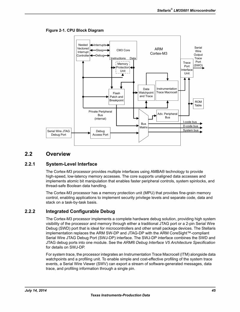
Figure 2-1. CPU Block Diagram
Private PeripheralBus
(internal)
DataWatchpointand Trace
Interrupts
Debug
Sleep
InstrumentationTrace Macrocell
TracePort
InterfaceUnit
CM3 Core
Instructions Data
FlashPatch andBreakpoint
MemoryProtection
Unit
DebugAccess Port
NestedVectoredInterruptController
Serial Wire JTAGDebug Port
BusMatrix
Adv. PeripheralBus
I-code busD-code busSystem bus
ROMTable
SerialWireOutputTracePort
(SWO)
ARMCortex-M3
2.2 Overview
2.2.1 System-Level InterfaceThe Cortex-M3 processor provides multiple interfaces using AMBA® technology to providehigh-speed, low-latency memory accesses. The core supports unaligned data accesses andimplements atomic bit manipulation that enables faster peripheral controls, system spinlocks, andthread-safe Boolean data handling.
The Cortex-M3 processor has a memory protection unit (MPU) that provides fine-grain memorycontrol, enabling applications to implement security privilege levels and separate code, data andstack on a task-by-task basis.
2.2.2 Integrated Configurable DebugThe Cortex-M3 processor implements a complete hardware debug solution, providing high systemvisibility of the processor and memory through either a traditional JTAG port or a 2-pin Serial WireDebug (SWD) port that is ideal for microcontrollers and other small package devices. The Stellarisimplementation replaces the ARM SW-DP and JTAG-DP with the ARM CoreSight™-compliantSerial Wire JTAG Debug Port (SWJ-DP) interface. The SWJ-DP interface combines the SWD andJTAG debug ports into one module. See the ARM® Debug Interface V5 Architecture Specificationfor details on SWJ-DP.
For system trace, the processor integrates an Instrumentation Trace Macrocell (ITM) alongside datawatchpoints and a profiling unit. To enable simple and cost-effective profiling of the system traceevents, a Serial Wire Viewer (SWV) can export a stream of software-generated messages, datatrace, and profiling information through a single pin.
45July 14, 2014Texas Instruments-Production Data
Stellaris® LM3S601 Microcontroller
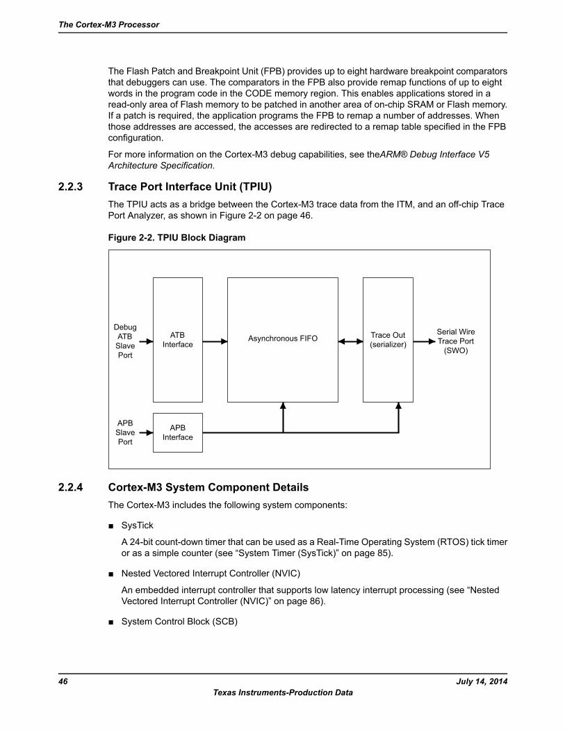
The Flash Patch and Breakpoint Unit (FPB) provides up to eight hardware breakpoint comparatorsthat debuggers can use. The comparators in the FPB also provide remap functions of up to eightwords in the program code in the CODE memory region. This enables applications stored in aread-only area of Flash memory to be patched in another area of on-chip SRAM or Flash memory.If a patch is required, the application programs the FPB to remap a number of addresses. Whenthose addresses are accessed, the accesses are redirected to a remap table specified in the FPBconfiguration.
For more information on the Cortex-M3 debug capabilities, see theARM® Debug Interface V5Architecture Specification.
2.2.3 Trace Port Interface Unit (TPIU)The TPIU acts as a bridge between the Cortex-M3 trace data from the ITM, and an off-chip TracePort Analyzer, as shown in Figure 2-2 on page 46.
Figure 2-2. TPIU Block Diagram
ATBInterface
Asynchronous FIFO
APBInterface
Trace Out(serializer)
DebugATBSlavePort
APBSlavePort
Serial WireTrace Port(SWO)
2.2.4 Cortex-M3 System Component DetailsThe Cortex-M3 includes the following system components:
SysTick
A 24-bit count-down timer that can be used as a Real-Time Operating System (RTOS) tick timeror as a simple counter (see “System Timer (SysTick)” on page 85).
Nested Vectored Interrupt Controller (NVIC)
An embedded interrupt controller that supports low latency interrupt processing (see “NestedVectored Interrupt Controller (NVIC)” on page 86).
System Control Block (SCB)
July 14, 201446Texas Instruments-Production Data
The Cortex-M3 Processor
The programming model interface to the processor. The SCB provides system implementationinformation and system control, including configuration, control, and reporting of system exceptions(see “System Control Block (SCB)” on page 88).
Memory Protection Unit (MPU)
Improves system reliability by defining the memory attributes for different memory regions. TheMPU provides up to eight different regions and an optional predefined background region (see“Memory Protection Unit (MPU)” on page 88).
2.3 Programming ModelThis section describes the Cortex-M3 programming model. In addition to the individual core registerdescriptions, information about the processor modes and privilege levels for software execution andstacks is included.
2.3.1 Processor Mode and Privilege Levels for Software ExecutionThe Cortex-M3 has two modes of operation:
Thread mode
Used to execute application software. The processor enters Thread mode when it comes out ofreset.
Handler mode
Used to handle exceptions. When the processor has finished exception processing, it returns toThread mode.
In addition, the Cortex-M3 has two privilege levels:
Unprivileged
In this mode, software has the following restrictions:
– Limited access to the MSR and MRS instructions and no use of the CPS instruction
– No access to the system timer, NVIC, or system control block
– Possibly restricted access to memory or peripherals
Privileged
In this mode, software can use all the instructions and has access to all resources.
In Thread mode, the CONTROL register (see page 61) controls whether software execution isprivileged or unprivileged. In Handler mode, software execution is always privileged.
Only privileged software can write to theCONTROL register to change the privilege level for softwareexecution in Thread mode. Unprivileged software can use the SVC instruction to make a supervisorcall to transfer control to privileged software.
2.3.2 StacksThe processor uses a full descending stack, meaning that the stack pointer indicates the last stackeditem on the memory. When the processor pushes a new item onto the stack, it decrements the stackpointer and then writes the item to the new memory location. The processor implements two stacks:
47July 14, 2014Texas Instruments-Production Data
Stellaris® LM3S601 Microcontroller
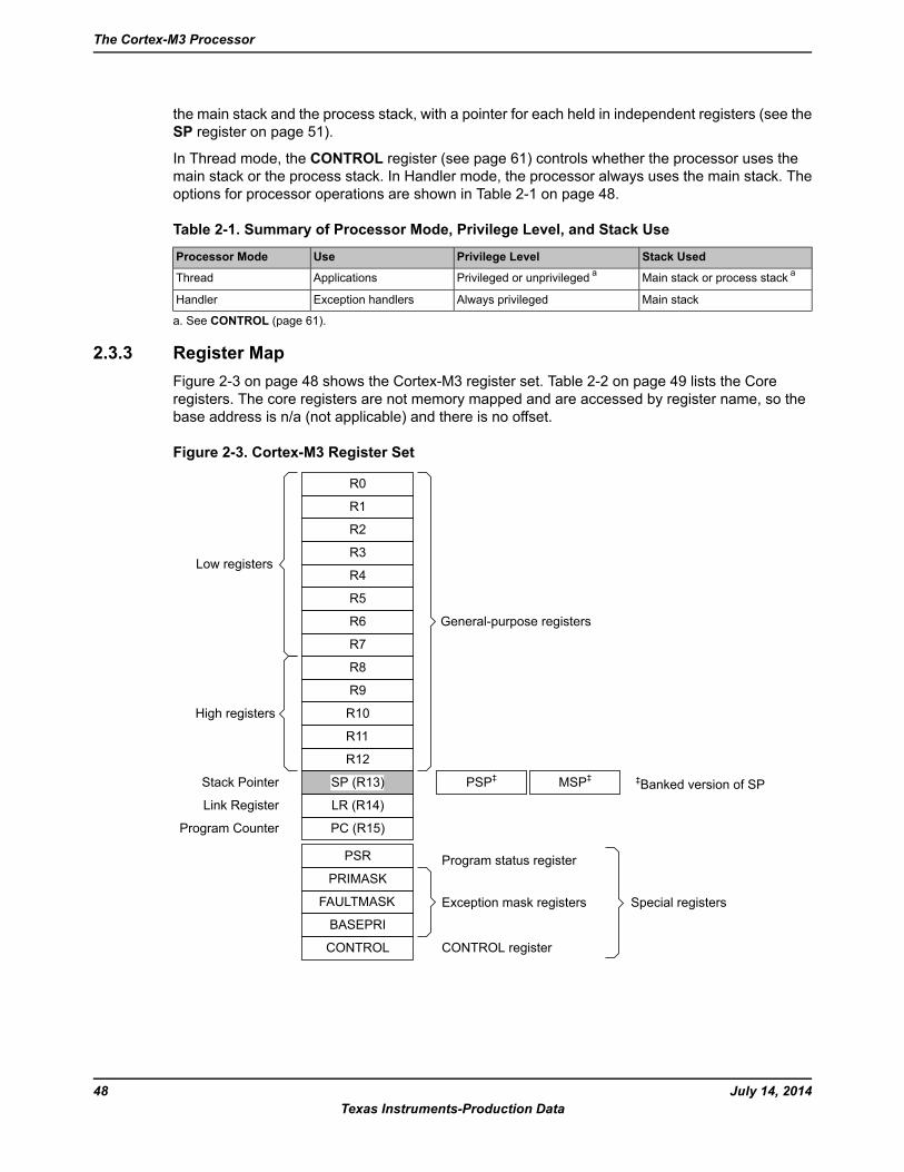
the main stack and the process stack, with a pointer for each held in independent registers (see theSP register on page 51).
In Thread mode, the CONTROL register (see page 61) controls whether the processor uses themain stack or the process stack. In Handler mode, the processor always uses the main stack. Theoptions for processor operations are shown in Table 2-1 on page 48.
Table 2-1. Summary of Processor Mode, Privilege Level, and Stack Use
Stack UsedPrivilege LevelUseProcessor Mode
Main stack or process stack aPrivileged or unprivileged aApplicationsThread
Main stackAlways privilegedException handlersHandler
a. See CONTROL (page 61).
2.3.3 Register MapFigure 2-3 on page 48 shows the Cortex-M3 register set. Table 2-2 on page 49 lists the Coreregisters. The core registers are not memory mapped and are accessed by register name, so thebase address is n/a (not applicable) and there is no offset.
Figure 2-3. Cortex-M3 Register Set
SP (R13)
LR (R14)
PC (R15)
R5
R6
R7
R0
R1
R3
R4
R2
R10
R11
R12
R8
R9
Low registers
High registers
MSP‡PSP‡
PSR
PRIMASK
FAULTMASK
BASEPRI
CONTROL
General-purpose registers
Stack Pointer
Link Register
Program Counter
Program status register
Exception mask registers
CONTROL register
Special registers
‡Banked version of SP
July 14, 201448Texas Instruments-Production Data
The Cortex-M3 Processor
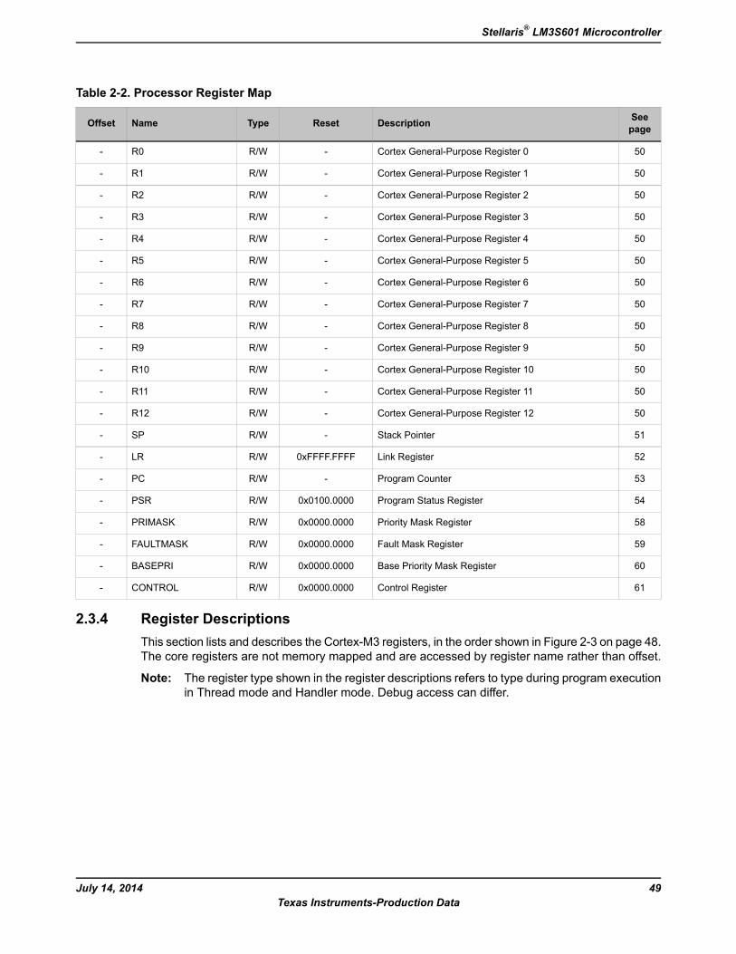
Table 2-2. Processor Register Map
SeepageDescriptionResetTypeNameOffset
50Cortex General-Purpose Register 0-R/WR0-
50Cortex General-Purpose Register 1-R/WR1-
50Cortex General-Purpose Register 2-R/WR2-
50Cortex General-Purpose Register 3-R/WR3-
50Cortex General-Purpose Register 4-R/WR4-
50Cortex General-Purpose Register 5-R/WR5-
50Cortex General-Purpose Register 6-R/WR6-
50Cortex General-Purpose Register 7-R/WR7-
50Cortex General-Purpose Register 8-R/WR8-
50Cortex General-Purpose Register 9-R/WR9-
50Cortex General-Purpose Register 10-R/WR10-
50Cortex General-Purpose Register 11-R/WR11-
50Cortex General-Purpose Register 12-R/WR12-
51Stack Pointer-R/WSP-
52Link Register0xFFFF.FFFFR/WLR-
53Program Counter-R/WPC-
54Program Status Register0x0100.0000R/WPSR-
58Priority Mask Register0x0000.0000R/WPRIMASK-
59Fault Mask Register0x0000.0000R/WFAULTMASK-
60Base Priority Mask Register0x0000.0000R/WBASEPRI-
61Control Register0x0000.0000R/WCONTROL-
2.3.4 Register DescriptionsThis section lists and describes the Cortex-M3 registers, in the order shown in Figure 2-3 on page 48.The core registers are not memory mapped and are accessed by register name rather than offset.
Note: The register type shown in the register descriptions refers to type during program executionin Thread mode and Handler mode. Debug access can differ.
49July 14, 2014Texas Instruments-Production Data
Stellaris® LM3S601 Microcontroller
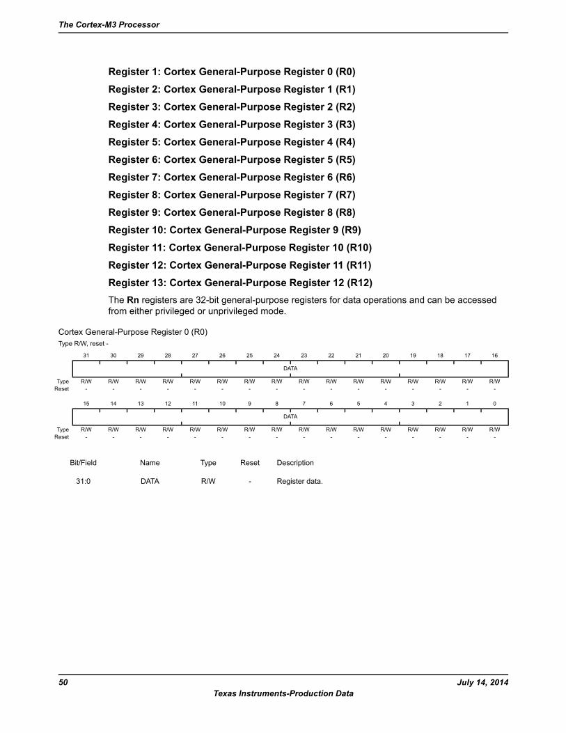
Register 1: Cortex General-Purpose Register 0 (R0)Register 2: Cortex General-Purpose Register 1 (R1)Register 3: Cortex General-Purpose Register 2 (R2)Register 4: Cortex General-Purpose Register 3 (R3)Register 5: Cortex General-Purpose Register 4 (R4)Register 6: Cortex General-Purpose Register 5 (R5)Register 7: Cortex General-Purpose Register 6 (R6)Register 8: Cortex General-Purpose Register 7 (R7)Register 9: Cortex General-Purpose Register 8 (R8)Register 10: Cortex General-Purpose Register 9 (R9)Register 11: Cortex General-Purpose Register 10 (R10)Register 12: Cortex General-Purpose Register 11 (R11)Register 13: Cortex General-Purpose Register 12 (R12)The Rn registers are 32-bit general-purpose registers for data operations and can be accessedfrom either privileged or unprivileged mode.
Cortex General-Purpose Register 0 (R0)Type R/W, reset -
16171819202122232425262728293031
DATA
R/WR/WR/WR/WR/WR/WR/WR/WR/WR/WR/WR/WR/WR/WR/WR/WType----------------Reset
0123456789101112131415
DATA
R/WR/WR/WR/WR/WR/WR/WR/WR/WR/WR/WR/WR/WR/WR/WR/WType----------------Reset
DescriptionResetTypeNameBit/Field
Register data.-R/WDATA31:0
July 14, 201450Texas Instruments-Production Data
The Cortex-M3 Processor
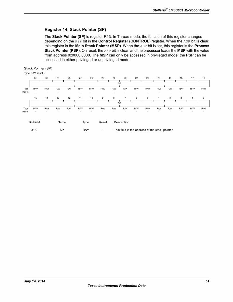
Register 14: Stack Pointer (SP)The Stack Pointer (SP) is register R13. In Thread mode, the function of this register changesdepending on the ASP bit in the Control Register (CONTROL) register. When the ASP bit is clear,this register is the Main Stack Pointer (MSP). When the ASP bit is set, this register is the ProcessStack Pointer (PSP). On reset, the ASP bit is clear, and the processor loads theMSP with the valuefrom address 0x0000.0000. The MSP can only be accessed in privileged mode; the PSP can beaccessed in either privileged or unprivileged mode.
Stack Pointer (SP)Type R/W, reset -
16171819202122232425262728293031
SP
R/WR/WR/WR/WR/WR/WR/WR/WR/WR/WR/WR/WR/WR/WR/WR/WType----------------Reset
0123456789101112131415
SP
R/WR/WR/WR/WR/WR/WR/WR/WR/WR/WR/WR/WR/WR/WR/WR/WType----------------Reset
DescriptionResetTypeNameBit/Field
This field is the address of the stack pointer.-R/WSP31:0
51July 14, 2014Texas Instruments-Production Data
Stellaris® LM3S601 Microcontroller
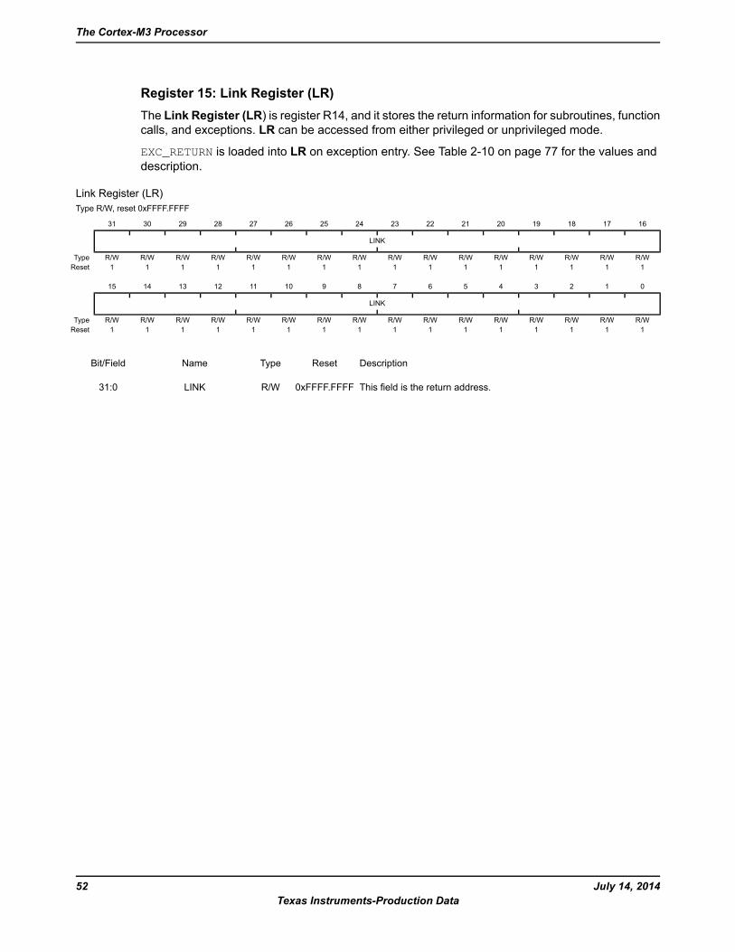
Register 15: Link Register (LR)The Link Register (LR) is register R14, and it stores the return information for subroutines, functioncalls, and exceptions. LR can be accessed from either privileged or unprivileged mode.
EXC_RETURN is loaded into LR on exception entry. See Table 2-10 on page 77 for the values anddescription.
Link Register (LR)Type R/W, reset 0xFFFF.FFFF
16171819202122232425262728293031
LINK
R/WR/WR/WR/WR/WR/WR/WR/WR/WR/WR/WR/WR/WR/WR/WR/WType1111111111111111Reset
0123456789101112131415
LINK
R/WR/WR/WR/WR/WR/WR/WR/WR/WR/WR/WR/WR/WR/WR/WR/WType1111111111111111Reset
DescriptionResetTypeNameBit/Field
This field is the return address.0xFFFF.FFFFR/WLINK31:0
July 14, 201452Texas Instruments-Production Data
The Cortex-M3 Processor
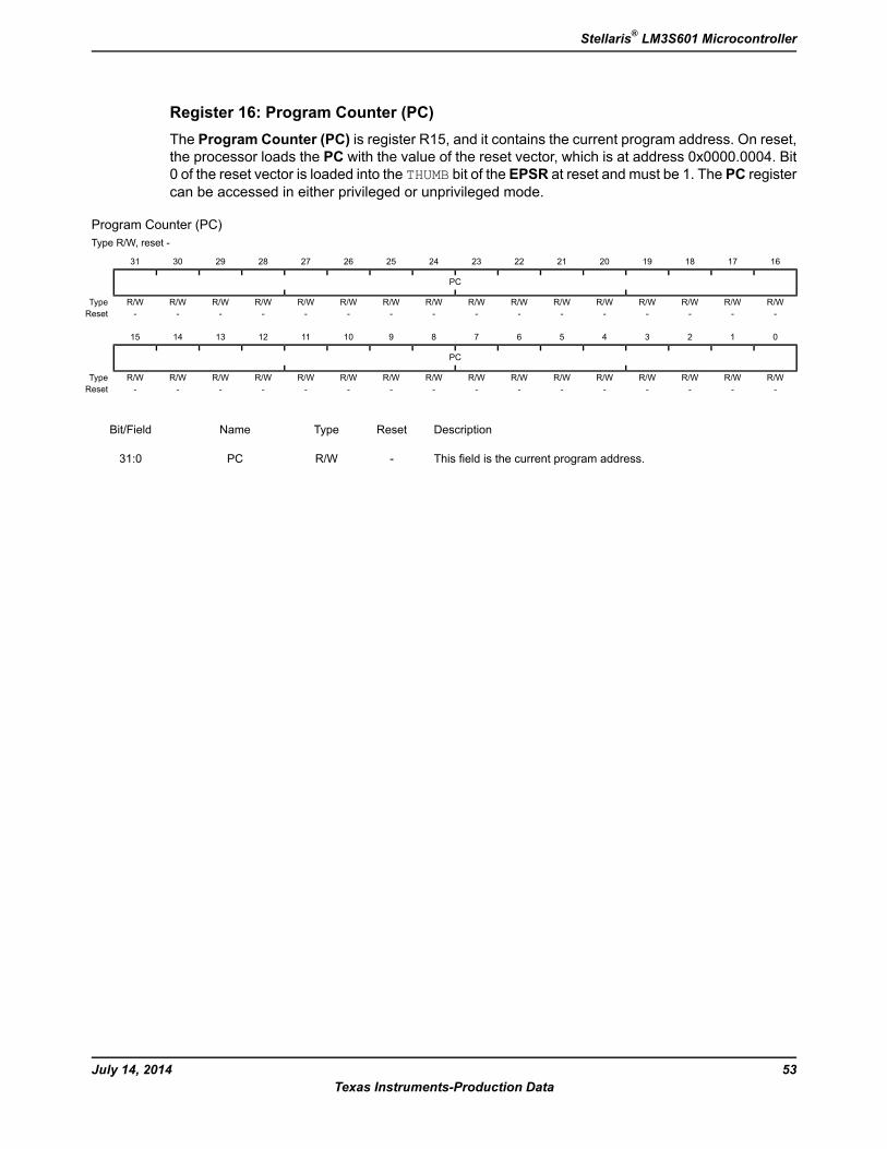
Register 16: Program Counter (PC)The Program Counter (PC) is register R15, and it contains the current program address. On reset,the processor loads the PC with the value of the reset vector, which is at address 0x0000.0004. Bit0 of the reset vector is loaded into the THUMB bit of the EPSR at reset and must be 1. The PC registercan be accessed in either privileged or unprivileged mode.
Program Counter (PC)Type R/W, reset -
16171819202122232425262728293031
PC
R/WR/WR/WR/WR/WR/WR/WR/WR/WR/WR/WR/WR/WR/WR/WR/WType----------------Reset
0123456789101112131415
PC
R/WR/WR/WR/WR/WR/WR/WR/WR/WR/WR/WR/WR/WR/WR/WR/WType----------------Reset
DescriptionResetTypeNameBit/Field
This field is the current program address.-R/WPC31:0
53July 14, 2014Texas Instruments-Production Data
Stellaris® LM3S601 Microcontroller
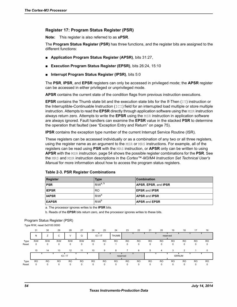
Register 17: Program Status Register (PSR)Note: This register is also referred to as xPSR.
The Program Status Register (PSR) has three functions, and the register bits are assigned to thedifferent functions:
Application Program Status Register (APSR), bits 31:27,
Execution Program Status Register (EPSR), bits 26:24, 15:10
Interrupt Program Status Register (IPSR), bits 5:0
The PSR, IPSR, and EPSR registers can only be accessed in privileged mode; the APSR registercan be accessed in either privileged or unprivileged mode.
APSR contains the current state of the condition flags from previous instruction executions.
EPSR contains the Thumb state bit and the execution state bits for the If-Then (IT) instruction orthe Interruptible-Continuable Instruction (ICI) field for an interrupted load multiple or store multipleinstruction. Attempts to read the EPSR directly through application software using the MSR instructionalways return zero. Attempts to write the EPSR using the MSR instruction in application softwareare always ignored. Fault handlers can examine the EPSR value in the stacked PSR to determinethe operation that faulted (see “Exception Entry and Return” on page 75).
IPSR contains the exception type number of the current Interrupt Service Routine (ISR).
These registers can be accessed individually or as a combination of any two or all three registers,using the register name as an argument to the MSR or MRS instructions. For example, all of theregisters can be read using PSR with the MRS instruction, or APSR only can be written to usingAPSR with the MSR instruction. page 54 shows the possible register combinations for the PSR. Seethe MRS and MSR instruction descriptions in the Cortex™-M3/M4 Instruction Set Technical User'sManual for more information about how to access the program status registers.
Table 2-3. PSR Register Combinations
CombinationTypeRegister
APSR, EPSR, and IPSRR/Wa, bPSR
EPSR and IPSRROIEPSR
APSR and IPSRR/WaIAPSR
APSR and EPSRR/WbEAPSR
a. The processor ignores writes to the IPSR bits.b. Reads of the EPSR bits return zero, and the processor ignores writes to these bits.
Program Status Register (PSR)Type R/W, reset 0x0100.0000
16171819202122232425262728293031
reservedTHUMBICI / ITQVCZN
ROROROROROROROROROROROR/WR/WR/WR/WR/WType0000000010000000Reset
0123456789101112131415
ISRNUMreservedICI / IT
ROROROROROROROROROROROROROROROROType0000000000000000Reset
July 14, 201454Texas Instruments-Production Data
The Cortex-M3 Processor
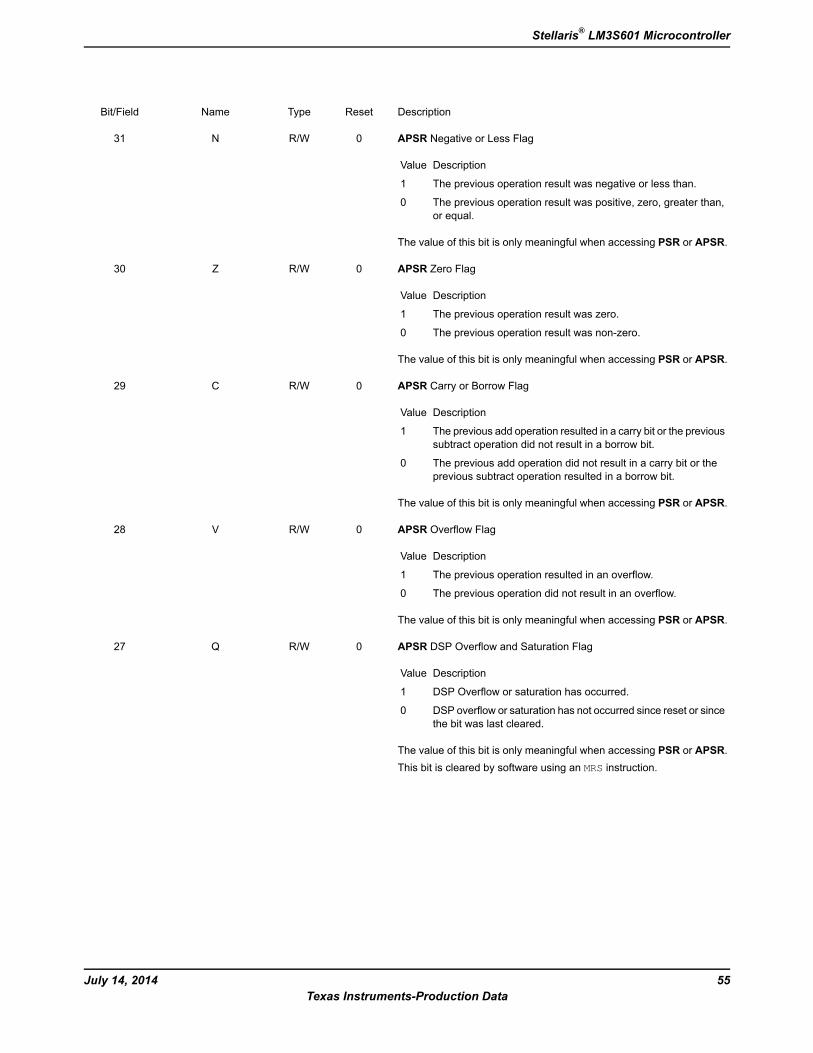
DescriptionResetTypeNameBit/Field
APSR Negative or Less Flag
DescriptionValue
The previous operation result was negative or less than.1
The previous operation result was positive, zero, greater than,or equal.
0
The value of this bit is only meaningful when accessing PSR or APSR.
0R/WN31
APSR Zero Flag
DescriptionValue
The previous operation result was zero.1
The previous operation result was non-zero.0
The value of this bit is only meaningful when accessing PSR or APSR.
0R/WZ30
APSR Carry or Borrow Flag
DescriptionValue
The previous add operation resulted in a carry bit or the previoussubtract operation did not result in a borrow bit.
1
The previous add operation did not result in a carry bit or theprevious subtract operation resulted in a borrow bit.
0
The value of this bit is only meaningful when accessing PSR or APSR.
0R/WC29
APSR Overflow Flag
DescriptionValue
The previous operation resulted in an overflow.1
The previous operation did not result in an overflow.0
The value of this bit is only meaningful when accessing PSR or APSR.
0R/WV28
APSR DSP Overflow and Saturation Flag
DescriptionValue
DSP Overflow or saturation has occurred.1
DSP overflow or saturation has not occurred since reset or sincethe bit was last cleared.
0
The value of this bit is only meaningful when accessing PSR or APSR.This bit is cleared by software using an MRS instruction.
0R/WQ27
55July 14, 2014Texas Instruments-Production Data
Stellaris® LM3S601 Microcontroller
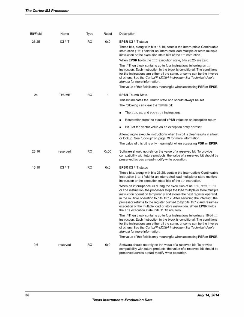
DescriptionResetTypeNameBit/Field
EPSR ICI / IT statusThese bits, along with bits 15:10, contain the Interruptible-ContinuableInstruction (ICI) field for an interrupted load multiple or store multipleinstruction or the execution state bits of the IT instruction.When EPSR holds the ICI execution state, bits 26:25 are zero.The If-Then block contains up to four instructions following an ITinstruction. Each instruction in the block is conditional. The conditionsfor the instructions are either all the same, or some can be the inverseof others. See the Cortex™-M3/M4 Instruction Set Technical User'sManual for more information.The value of this field is only meaningful when accessingPSR or EPSR.
0x0ROICI / IT26:25
EPSR Thumb StateThis bit indicates the Thumb state and should always be set.The following can clear the THUMB bit:
The BLX, BX and POPPC instructions
Restoration from the stacked xPSR value on an exception return
Bit 0 of the vector value on an exception entry or reset
Attempting to execute instructions when this bit is clear results in a faultor lockup. See “Lockup” on page 79 for more information.The value of this bit is only meaningful when accessing PSR or EPSR.
1ROTHUMB24
Software should not rely on the value of a reserved bit. To providecompatibility with future products, the value of a reserved bit should bepreserved across a read-modify-write operation.
0x00ROreserved23:16
EPSR ICI / IT statusThese bits, along with bits 26:25, contain the Interruptible-ContinuableInstruction (ICI) field for an interrupted load multiple or store multipleinstruction or the execution state bits of the IT instruction.When an interrupt occurs during the execution of an LDM, STM, PUSHor POP instruction, the processor stops the load multiple or store multipleinstruction operation temporarily and stores the next register operandin the multiple operation to bits 15:12. After servicing the interrupt, theprocessor returns to the register pointed to by bits 15:12 and resumesexecution of the multiple load or store instruction. When EPSR holdsthe ICI execution state, bits 11:10 are zero.The If-Then block contains up to four instructions following a 16-bit ITinstruction. Each instruction in the block is conditional. The conditionsfor the instructions are either all the same, or some can be the inverseof others. See the Cortex™-M3/M4 Instruction Set Technical User'sManual for more information.The value of this field is only meaningful when accessingPSR or EPSR.
0x0ROICI / IT15:10
Software should not rely on the value of a reserved bit. To providecompatibility with future products, the value of a reserved bit should bepreserved across a read-modify-write operation.
0x0ROreserved9:6
July 14, 201456Texas Instruments-Production Data
The Cortex-M3 Processor
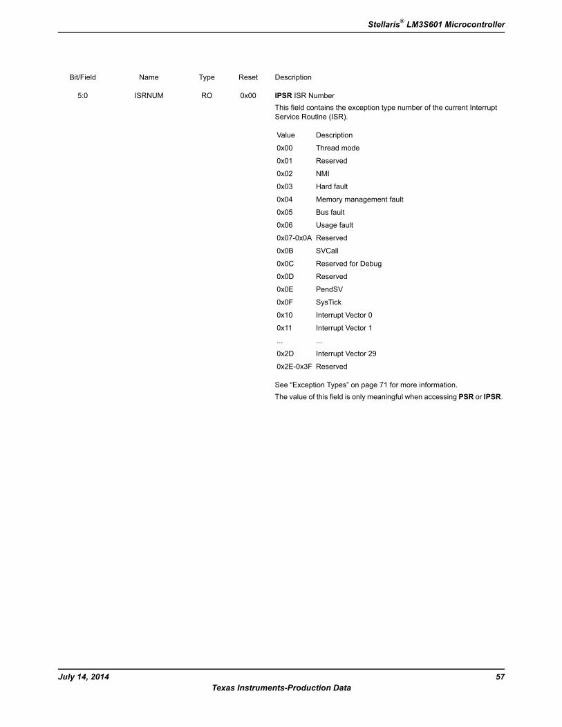
DescriptionResetTypeNameBit/Field
IPSR ISR NumberThis field contains the exception type number of the current InterruptService Routine (ISR).
DescriptionValue
Thread mode0x00
Reserved0x01
NMI0x02
Hard fault0x03
Memory management fault0x04
Bus fault0x05
Usage fault0x06
Reserved0x07-0x0A
SVCall0x0B
Reserved for Debug0x0C
Reserved0x0D
PendSV0x0E
SysTick0x0F
Interrupt Vector 00x10
Interrupt Vector 10x11
......
Interrupt Vector 290x2D
Reserved0x2E-0x3F
See “Exception Types” on page 71 for more information.The value of this field is only meaningful when accessing PSR or IPSR.
0x00ROISRNUM5:0
57July 14, 2014Texas Instruments-Production Data
Stellaris® LM3S601 Microcontroller
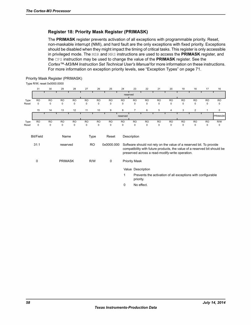
Register 18: Priority Mask Register (PRIMASK)The PRIMASK register prevents activation of all exceptions with programmable priority. Reset,non-maskable interrupt (NMI), and hard fault are the only exceptions with fixed priority. Exceptionsshould be disabled when they might impact the timing of critical tasks. This register is only accessiblein privileged mode. The MSR and MRS instructions are used to access the PRIMASK register, andthe CPS instruction may be used to change the value of the PRIMASK register. See theCortex™-M3/M4 Instruction Set Technical User's Manual for more information on these instructions.For more information on exception priority levels, see “Exception Types” on page 71.
Priority Mask Register (PRIMASK)Type R/W, reset 0x0000.0000
16171819202122232425262728293031
reserved
ROROROROROROROROROROROROROROROROType0000000000000000Reset
0123456789101112131415
PRIMASKreserved
R/WROROROROROROROROROROROROROROROType0000000000000000Reset
DescriptionResetTypeNameBit/Field
Software should not rely on the value of a reserved bit. To providecompatibility with future products, the value of a reserved bit should bepreserved across a read-modify-write operation.
0x0000.000ROreserved31:1
Priority Mask
DescriptionValue
Prevents the activation of all exceptions with configurablepriority.
1
No effect.0
0R/WPRIMASK0
July 14, 201458Texas Instruments-Production Data
The Cortex-M3 Processor
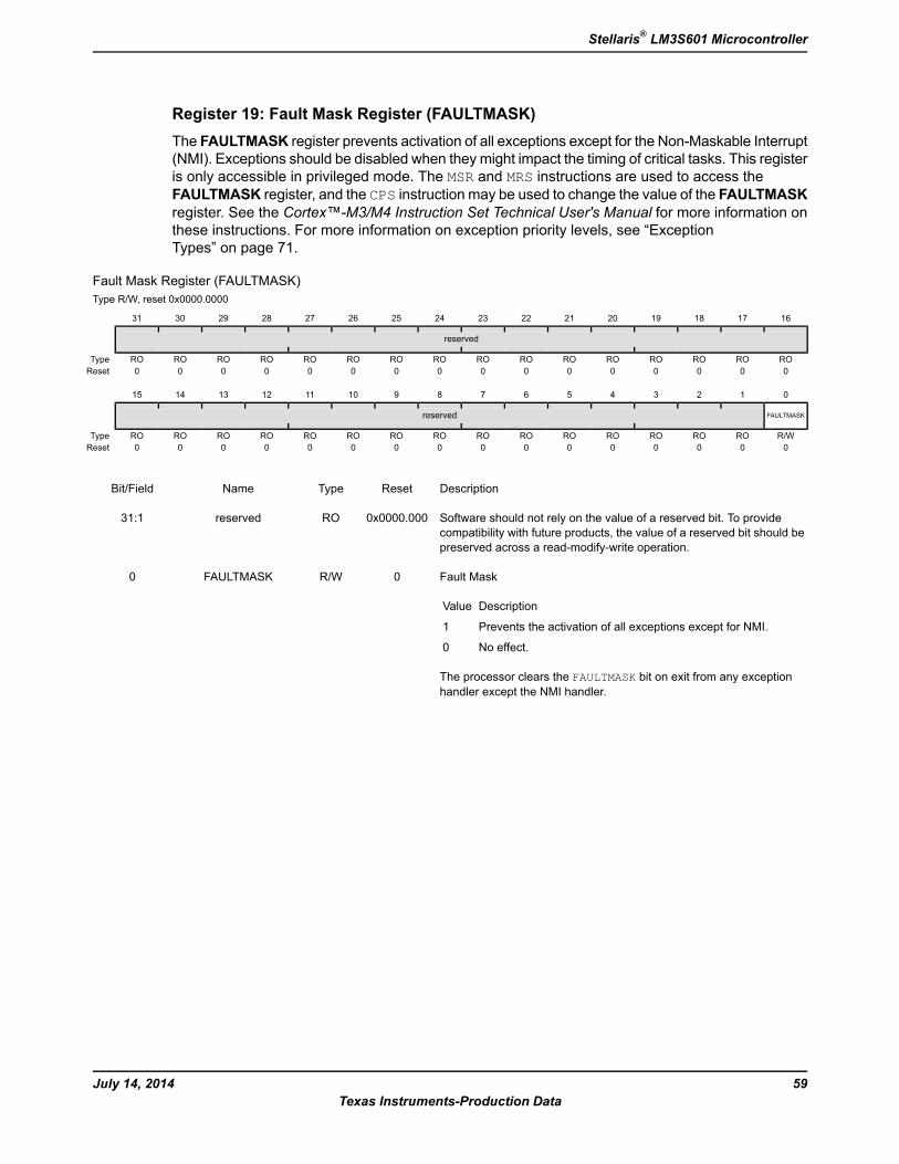
Register 19: Fault Mask Register (FAULTMASK)The FAULTMASK register prevents activation of all exceptions except for the Non-Maskable Interrupt(NMI). Exceptions should be disabled when they might impact the timing of critical tasks. This registeris only accessible in privileged mode. The MSR and MRS instructions are used to access theFAULTMASK register, and the CPS instruction may be used to change the value of the FAULTMASKregister. See the Cortex™-M3/M4 Instruction Set Technical User's Manual for more information onthese instructions. For more information on exception priority levels, see “ExceptionTypes” on page 71.
Fault Mask Register (FAULTMASK)Type R/W, reset 0x0000.0000
16171819202122232425262728293031
reserved
ROROROROROROROROROROROROROROROROType0000000000000000Reset
0123456789101112131415
FAULTMASKreserved
R/WROROROROROROROROROROROROROROROType0000000000000000Reset
DescriptionResetTypeNameBit/Field
Software should not rely on the value of a reserved bit. To providecompatibility with future products, the value of a reserved bit should bepreserved across a read-modify-write operation.
0x0000.000ROreserved31:1
Fault Mask
DescriptionValue
Prevents the activation of all exceptions except for NMI.1
No effect.0
The processor clears the FAULTMASK bit on exit from any exceptionhandler except the NMI handler.
0R/WFAULTMASK0
59July 14, 2014Texas Instruments-Production Data
Stellaris® LM3S601 Microcontroller
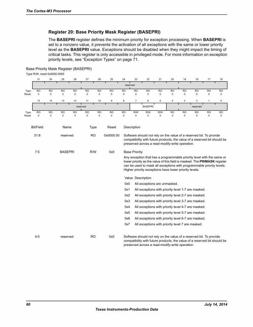
Register 20: Base Priority Mask Register (BASEPRI)The BASEPRI register defines the minimum priority for exception processing. When BASEPRI isset to a nonzero value, it prevents the activation of all exceptions with the same or lower prioritylevel as the BASEPRI value. Exceptions should be disabled when they might impact the timing ofcritical tasks. This register is only accessible in privileged mode. For more information on exceptionpriority levels, see “Exception Types” on page 71.
Base Priority Mask Register (BASEPRI)Type R/W, reset 0x0000.0000
16171819202122232425262728293031
reserved
ROROROROROROROROROROROROROROROROType0000000000000000Reset
0123456789101112131415
reservedBASEPRIreserved
ROROROROROR/WR/WR/WROROROROROROROROType0000000000000000Reset
DescriptionResetTypeNameBit/Field
Software should not rely on the value of a reserved bit. To providecompatibility with future products, the value of a reserved bit should bepreserved across a read-modify-write operation.
0x0000.00ROreserved31:8
Base PriorityAny exception that has a programmable priority level with the same orlower priority as the value of this field is masked. The PRIMASK registercan be used to mask all exceptions with programmable priority levels.Higher priority exceptions have lower priority levels.
DescriptionValue
All exceptions are unmasked.0x0
All exceptions with priority level 1-7 are masked.0x1
All exceptions with priority level 2-7 are masked.0x2
All exceptions with priority level 3-7 are masked.0x3
All exceptions with priority level 4-7 are masked.0x4
All exceptions with priority level 5-7 are masked.0x5
All exceptions with priority level 6-7 are masked.0x6
All exceptions with priority level 7 are masked.0x7
0x0R/WBASEPRI7:5
Software should not rely on the value of a reserved bit. To providecompatibility with future products, the value of a reserved bit should bepreserved across a read-modify-write operation.
0x0ROreserved4:0
July 14, 201460Texas Instruments-Production Data
The Cortex-M3 Processor
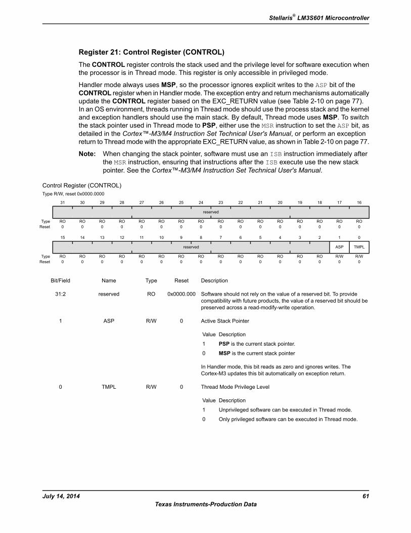
Register 21: Control Register (CONTROL)The CONTROL register controls the stack used and the privilege level for software execution whenthe processor is in Thread mode. This register is only accessible in privileged mode.
Handler mode always uses MSP, so the processor ignores explicit writes to the ASP bit of theCONTROL register when in Handler mode. The exception entry and returnmechanisms automaticallyupdate the CONTROL register based on the EXC_RETURN value (see Table 2-10 on page 77).In an OS environment, threads running in Thread mode should use the process stack and the kerneland exception handlers should use the main stack. By default, Thread mode uses MSP. To switchthe stack pointer used in Thread mode to PSP, either use the MSR instruction to set the ASP bit, asdetailed in the Cortex™-M3/M4 Instruction Set Technical User's Manual, or perform an exceptionreturn to Threadmode with the appropriate EXC_RETURN value, as shown in Table 2-10 on page 77.
Note: When changing the stack pointer, software must use an ISB instruction immediately afterthe MSR instruction, ensuring that instructions after the ISB execute use the new stackpointer. See the Cortex™-M3/M4 Instruction Set Technical User's Manual.
Control Register (CONTROL)Type R/W, reset 0x0000.0000
16171819202122232425262728293031
reserved
ROROROROROROROROROROROROROROROROType0000000000000000Reset
0123456789101112131415
TMPLASPreserved
R/WR/WROROROROROROROROROROROROROROType0000000000000000Reset
DescriptionResetTypeNameBit/Field
Software should not rely on the value of a reserved bit. To providecompatibility with future products, the value of a reserved bit should bepreserved across a read-modify-write operation.
0x0000.000ROreserved31:2
Active Stack Pointer
DescriptionValue
PSP is the current stack pointer.1
MSP is the current stack pointer0
In Handler mode, this bit reads as zero and ignores writes. TheCortex-M3 updates this bit automatically on exception return.
0R/WASP1
Thread Mode Privilege Level
DescriptionValue
Unprivileged software can be executed in Thread mode.1
Only privileged software can be executed in Thread mode.0
0R/WTMPL0
61July 14, 2014Texas Instruments-Production Data
Stellaris® LM3S601 Microcontroller
2.3.5 Exceptions and InterruptsThe Cortex-M3 processor supports interrupts and system exceptions. The processor and the NestedVectored Interrupt Controller (NVIC) prioritize and handle all exceptions. An exception changes thenormal flow of software control. The processor uses Handler mode to handle all exceptions exceptfor reset. See “Exception Entry and Return” on page 75 for more information.
The NVIC registers control interrupt handling. See “Nested Vectored Interrupt Controller(NVIC)” on page 86 for more information.
2.3.6 Data TypesThe Cortex-M3 supports 32-bit words, 16-bit halfwords, and 8-bit bytes. The processor also supports64-bit data transfer instructions. All instruction and data memory accesses are little endian. See“Memory Regions, Types and Attributes” on page 63 for more information.
2.4 Memory ModelThis section describes the processor memory map, the behavior of memory accesses, and thebit-banding features. The processor has a fixed memory map that provides up to 4 GB of addressablememory.
The memory map for the LM3S601 controller is provided in Table 2-4 on page 62. In this manual,register addresses are given as a hexadecimal increment, relative to the module’s base addressas shown in the memory map.
The regions for SRAM and peripherals include bit-band regions. Bit-banding provides atomicoperations to bit data (see “Bit-Banding” on page 66).
The processor reserves regions of the Private peripheral bus (PPB) address range for core peripheralregisters (see “Cortex-M3 Peripherals” on page 85).
Note: Within the memory map, all reserved space returns a bus fault when read or written.
Table 2-4. Memory Map
For details,see page ...
DescriptionEndStart
Memory
218On-chip Flash0x0000.7FFF0x0000.0000
-Reserved0x1FFF.FFFF0x0000.8000
212Bit-banded on-chip SRAM0x2000.1FFF0x2000.0000
-Reserved0x21FF.FFFF0x2000.2000
212Bit-band alias of bit-banded on-chip SRAM starting at0x2000.0000
0x2203.FFFF0x2200.0000
-Reserved0x3FFF.FFFF0x2204.0000
FiRM Peripherals
311Watchdog timer 00x4000.0FFF0x4000.0000
-Reserved0x4000.3FFF0x4000.1000
240GPIO Port A0x4000.4FFF0x4000.4000
240GPIO Port B0x4000.5FFF0x4000.5000
240GPIO Port C0x4000.6FFF0x4000.6000
240GPIO Port D0x4000.7FFF0x4000.7000
384SSI00x4000.8FFF0x4000.8000
July 14, 201462Texas Instruments-Production Data
The Cortex-M3 Processor
Table 2-4. Memory Map (continued)
For details,see page ...
DescriptionEndStart
-Reserved0x4000.BFFF0x4000.9000
339UART00x4000.CFFF0x4000.C000
339UART10x4000.DFFF0x4000.D000
-Reserved0x4001.FFFF0x4000.E000
Peripherals
425I2C 00x4002.0FFF0x4002.0000
-Reserved0x4002.3FFF0x4002.1000
240GPIO Port E0x4002.4FFF0x4002.4000
-Reserved0x4002.7FFF0x4002.5000
469PWM0x4002.8FFF0x4002.8000
-Reserved0x4002.BFFF0x4002.9000
503QEI00x4002.CFFF0x4002.C000
-Reserved0x4002.FFFF0x4002.D000
283Timer 00x4003.0FFF0x4003.0000
283Timer 10x4003.1FFF0x4003.1000
283Timer 20x4003.2FFF0x4003.2000
-Reserved0x4003.BFFF0x4003.3000
447Analog Comparators0x4003.CFFF0x4003.C000
-Reserved0x400F.CFFF0x4003.D000
218Flash memory control0x400F.DFFF0x400F.D000
164System control0x400F.EFFF0x400F.E000
-Reserved0x41FF.FFFF0x400F.F000
-Bit-banded alias of 0x4000.0000 through 0x400F.FFFF0x43FF.FFFF0x4200.0000
-Reserved0xDFFF.FFFF0x4400.0000
Private Peripheral Bus
45Instrumentation Trace Macrocell (ITM)0xE000.0FFF0xE000.0000
45Data Watchpoint and Trace (DWT)0xE000.1FFF0xE000.1000
45Flash Patch and Breakpoint (FPB)0xE000.2FFF0xE000.2000
-Reserved0xE000.DFFF0xE000.3000
93Cortex-M3 Peripherals (SysTick, NVIC, MPU and SCB)0xE000.EFFF0xE000.E000
-Reserved0xE003.FFFF0xE000.F000
46Trace Port Interface Unit (TPIU)0xE004.0FFF0xE004.0000
-Reserved0xFFFF.FFFF0xE004.1000
2.4.1 Memory Regions, Types and AttributesThe memory map and the programming of the MPU split the memory map into regions. Each regionhas a defined memory type, and some regions have additional memory attributes. The memorytype and attributes determine the behavior of accesses to the region.
The memory types are:
Normal: The processor can re-order transactions for efficiency and perform speculative reads.
63July 14, 2014Texas Instruments-Production Data
Stellaris® LM3S601 Microcontroller
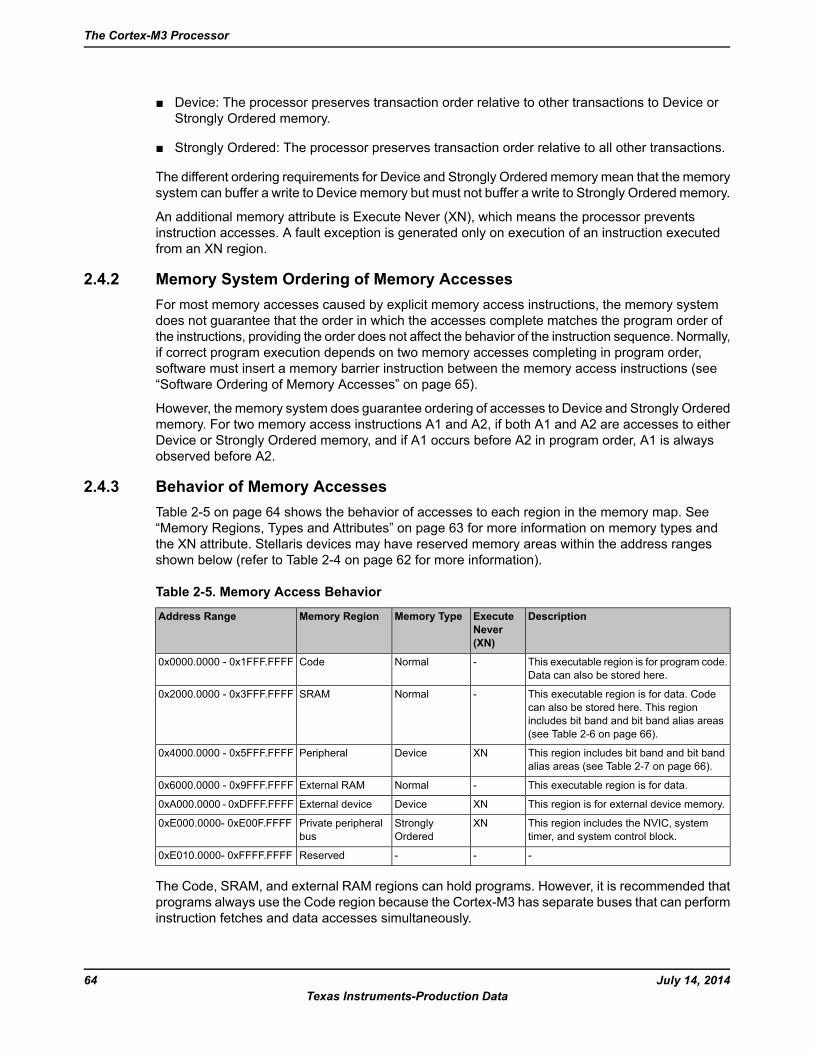
Device: The processor preserves transaction order relative to other transactions to Device orStrongly Ordered memory.
Strongly Ordered: The processor preserves transaction order relative to all other transactions.
The different ordering requirements for Device and Strongly Ordered memory mean that the memorysystem can buffer a write to Device memory but must not buffer a write to Strongly Ordered memory.
An additional memory attribute is Execute Never (XN), which means the processor preventsinstruction accesses. A fault exception is generated only on execution of an instruction executedfrom an XN region.
2.4.2 Memory System Ordering of Memory AccessesFor most memory accesses caused by explicit memory access instructions, the memory systemdoes not guarantee that the order in which the accesses complete matches the program order ofthe instructions, providing the order does not affect the behavior of the instruction sequence. Normally,if correct program execution depends on two memory accesses completing in program order,software must insert a memory barrier instruction between the memory access instructions (see“Software Ordering of Memory Accesses” on page 65).
However, the memory system does guarantee ordering of accesses to Device and Strongly Orderedmemory. For two memory access instructions A1 and A2, if both A1 and A2 are accesses to eitherDevice or Strongly Ordered memory, and if A1 occurs before A2 in program order, A1 is alwaysobserved before A2.
2.4.3 Behavior of Memory AccessesTable 2-5 on page 64 shows the behavior of accesses to each region in the memory map. See“Memory Regions, Types and Attributes” on page 63 for more information on memory types andthe XN attribute. Stellaris devices may have reserved memory areas within the address rangesshown below (refer to Table 2-4 on page 62 for more information).
Table 2-5. Memory Access Behavior
DescriptionExecuteNever(XN)
Memory TypeMemory RegionAddress Range
This executable region is for program code.Data can also be stored here.
-NormalCode0x0000.0000 - 0x1FFF.FFFF
This executable region is for data. Codecan also be stored here. This regionincludes bit band and bit band alias areas(see Table 2-6 on page 66).
-NormalSRAM0x2000.0000 - 0x3FFF.FFFF
This region includes bit band and bit bandalias areas (see Table 2-7 on page 66).
XNDevicePeripheral0x4000.0000 - 0x5FFF.FFFF
This executable region is for data.-NormalExternal RAM0x6000.0000 - 0x9FFF.FFFF
This region is for external device memory.XNDeviceExternal device0xA000.0000 - 0xDFFF.FFFF
This region includes the NVIC, systemtimer, and system control block.
XNStronglyOrdered
Private peripheralbus
0xE000.0000- 0xE00F.FFFF
---Reserved0xE010.0000- 0xFFFF.FFFF
The Code, SRAM, and external RAM regions can hold programs. However, it is recommended thatprograms always use the Code region because the Cortex-M3 has separate buses that can performinstruction fetches and data accesses simultaneously.
July 14, 201464Texas Instruments-Production Data
The Cortex-M3 Processor
The MPU can override the default memory access behavior described in this section. For moreinformation, see “Memory Protection Unit (MPU)” on page 88.
The Cortex-M3 prefetches instructions ahead of execution and speculatively prefetches from branchtarget addresses.
2.4.4 Software Ordering of Memory AccessesThe order of instructions in the program flow does not always guarantee the order of thecorresponding memory transactions for the following reasons:
The processor can reorder some memory accesses to improve efficiency, providing this doesnot affect the behavior of the instruction sequence.
The processor has multiple bus interfaces.
Memory or devices in the memory map have different wait states.
Some memory accesses are buffered or speculative.
“Memory SystemOrdering of Memory Accesses” on page 64 describes the cases where the memorysystem guarantees the order of memory accesses. Otherwise, if the order of memory accesses iscritical, software must include memory barrier instructions to force that ordering. The Cortex-M3has the following memory barrier instructions:
The Data Memory Barrier (DMB) instruction ensures that outstanding memory transactionscomplete before subsequent memory transactions.
The Data Synchronization Barrier (DSB) instruction ensures that outstanding memory transactionscomplete before subsequent instructions execute.
The Instruction Synchronization Barrier (ISB) instruction ensures that the effect of all completedmemory transactions is recognizable by subsequent instructions.
Memory barrier instructions can be used in the following situations:
MPU programming
– If the MPU settings are changed and the change must be effective on the very next instruction,use a DSB instruction to ensure the effect of the MPU takes place immediately at the end ofcontext switching.
– Use an ISB instruction to ensure the new MPU setting takes effect immediately afterprogramming the MPU region or regions, if the MPU configuration code was accessed usinga branch or call. If the MPU configuration code is entered using exception mechanisms, thenan ISB instruction is not required.
Vector table
If the program changes an entry in the vector table and then enables the corresponding exception,use a DMB instruction between the operations. The DMB instruction ensures that if the exceptionis taken immediately after being enabled, the processor uses the new exception vector.
Self-modifying code
65July 14, 2014Texas Instruments-Production Data
Stellaris® LM3S601 Microcontroller
If a program contains self-modifying code, use an ISB instruction immediately after the codemodification in the program. The ISB instruction ensures subsequent instruction execution usesthe updated program.
Memory map switching
If the system contains a memory map switching mechanism, use a DSB instruction after switchingthe memory map in the program. The DSB instruction ensures subsequent instruction executionuses the updated memory map.
Dynamic exception priority change
When an exception priority has to change when the exception is pending or active, use DSBinstructions after the change. The change then takes effect on completion of the DSB instruction.
Memory accesses to Strongly Ordered memory, such as the System Control Block, do not requirethe use of DMB instructions.
For more information on the memory barrier instructions, see the Cortex™-M3/M4 Instruction SetTechnical User's Manual.
2.4.5 Bit-BandingA bit-band region maps each word in a bit-band alias region to a single bit in the bit-band region.The bit-band regions occupy the lowest 1 MB of the SRAM and peripheral memory regions. Accessesto the 32-MB SRAM alias region map to the 1-MB SRAM bit-band region, as shown in Table2-6 on page 66. Accesses to the 32-MB peripheral alias region map to the 1-MB peripheral bit-bandregion, as shown in Table 2-7 on page 66. For the specific address range of the bit-band regions,see Table 2-4 on page 62.
Note: A word access to the SRAM or the peripheral bit-band alias region maps to a single bit inthe SRAM or peripheral bit-band region.
A word access to a bit band address results in a word access to the underlying memory,and similarly for halfword and byte accesses. This allows bit band accesses to match theaccess requirements of the underlying peripheral.
Table 2-6. SRAM Memory Bit-Banding Regions
Instruction and Data AccessesMemory RegionAddress Range
EndStart
Direct accesses to this memory range behave as SRAMmemory accesses, but this region is also bit addressablethrough bit-band alias.
SRAM bit-band region0x2000.1FFF0x2000.0000
Data accesses to this region are remapped to bit bandregion. A write operation is performed asread-modify-write. Instruction accesses are not remapped.
SRAM bit-band alias0x2203.FFFF0x2200.0000
Table 2-7. Peripheral Memory Bit-Banding Regions
Instruction and Data AccessesMemory RegionAddress Range
EndStart
Direct accesses to this memory range behave asperipheral memory accesses, but this region is also bitaddressable through bit-band alias.
Peripheral bit-bandregion
0x400F.FFFF0x4000.0000
July 14, 201466Texas Instruments-Production Data
The Cortex-M3 Processor
Table 2-7. Peripheral Memory Bit-Banding Regions (continued)
Instruction and Data AccessesMemory RegionAddress Range
EndStart
Data accesses to this region are remapped to bit bandregion. A write operation is performed asread-modify-write. Instruction accesses are not permitted.
Peripheral bit-band alias0x43FF.FFFF0x4200.0000
The following formula shows how the alias region maps onto the bit-band region:
bit_word_offset = (byte_offset x 32) + (bit_number x 4)
bit_word_addr = bit_band_base + bit_word_offset
where:
bit_word_offsetThe position of the target bit in the bit-band memory region.
bit_word_addrThe address of the word in the alias memory region that maps to the targeted bit.
bit_band_baseThe starting address of the alias region.
byte_offsetThe number of the byte in the bit-band region that contains the targeted bit.
bit_numberThe bit position, 0-7, of the targeted bit.
Figure 2-4 on page 68 shows examples of bit-band mapping between the SRAM bit-band aliasregion and the SRAM bit-band region:
The alias word at 0x23FF.FFE0 maps to bit 0 of the bit-band byte at 0x200F.FFFF:
0x23FF.FFE0 = 0x2200.0000 + (0x000F.FFFF*32) + (0*4)
The alias word at 0x23FF.FFFC maps to bit 7 of the bit-band byte at 0x200F.FFFF:
0x23FF.FFFC = 0x2200.0000 + (0x000F.FFFF*32) + (7*4)
The alias word at 0x2200.0000 maps to bit 0 of the bit-band byte at 0x2000.0000:
0x2200.0000 = 0x2200.0000 + (0*32) + (0*4)
The alias word at 0x2200.001C maps to bit 7 of the bit-band byte at 0x2000.0000:
0x2200.001C = 0x2200.0000+ (0*32) + (7*4)
67July 14, 2014Texas Instruments-Production Data
Stellaris® LM3S601 Microcontroller
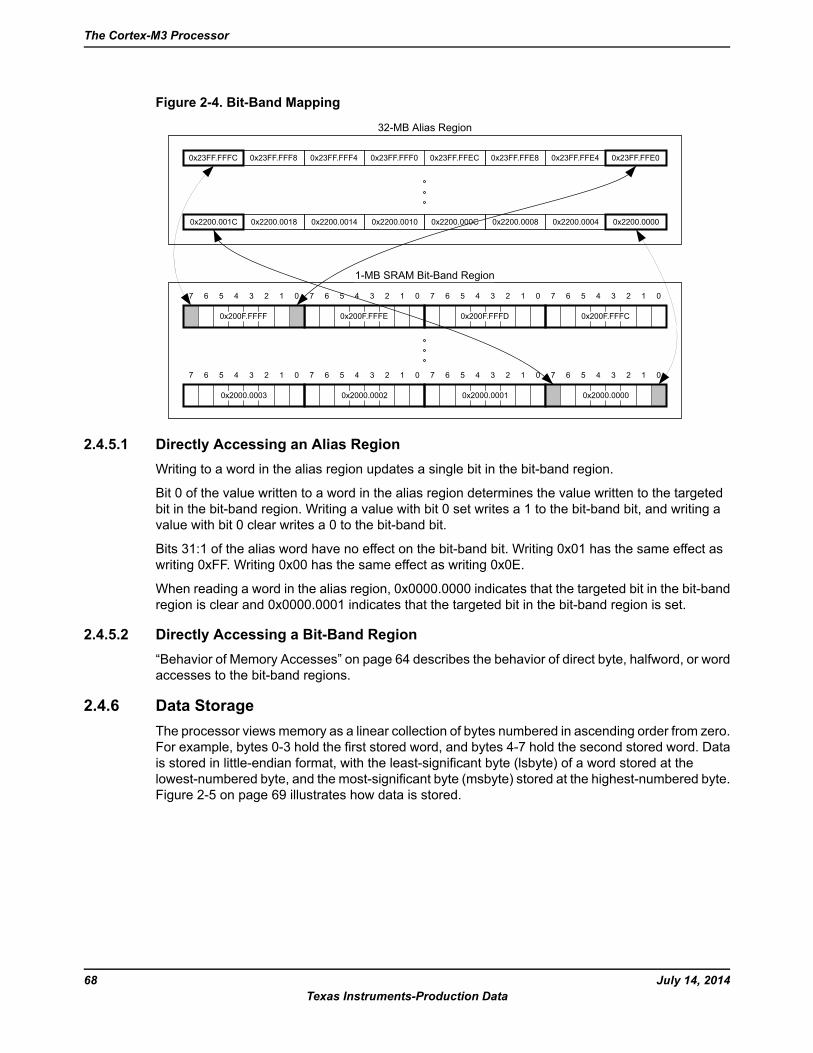
Figure 2-4. Bit-Band Mapping
0x23FF.FFE4
0x2200.0004
0x23FF.FFE00x23FF.FFE80x23FF.FFEC0x23FF.FFF00x23FF.FFF40x23FF.FFF80x23FF.FFFC
0x2200.00000x2200.00140x2200.00180x2200.001C 0x2200.00080x2200.0010 0x2200.000C
32-MB Alias Region
0
7 0
07
0x2000.00000x2000.00010x2000.00020x2000.0003
6 5 4 3 2 1 07 6 5 4 3 2 1 7 6 5 4 3 2 1 07 6 5 4 3 2 1
07 6 5 4 3 2 1 6 5 4 3 2 107 6 5 4 3 2 1 07 6 5 4 3 2 1
0x200F.FFFC0x200F.FFFD0x200F.FFFE0x200F.FFFF
1-MB SRAM Bit-Band Region
2.4.5.1 Directly Accessing an Alias RegionWriting to a word in the alias region updates a single bit in the bit-band region.
Bit 0 of the value written to a word in the alias region determines the value written to the targetedbit in the bit-band region. Writing a value with bit 0 set writes a 1 to the bit-band bit, and writing avalue with bit 0 clear writes a 0 to the bit-band bit.
Bits 31:1 of the alias word have no effect on the bit-band bit. Writing 0x01 has the same effect aswriting 0xFF. Writing 0x00 has the same effect as writing 0x0E.
When reading a word in the alias region, 0x0000.0000 indicates that the targeted bit in the bit-bandregion is clear and 0x0000.0001 indicates that the targeted bit in the bit-band region is set.
2.4.5.2 Directly Accessing a Bit-Band Region“Behavior of Memory Accesses” on page 64 describes the behavior of direct byte, halfword, or wordaccesses to the bit-band regions.
2.4.6 Data StorageThe processor views memory as a linear collection of bytes numbered in ascending order from zero.For example, bytes 0-3 hold the first stored word, and bytes 4-7 hold the second stored word. Datais stored in little-endian format, with the least-significant byte (lsbyte) of a word stored at thelowest-numbered byte, and the most-significant byte (msbyte) stored at the highest-numbered byte.Figure 2-5 on page 69 illustrates how data is stored.
July 14, 201468Texas Instruments-Production Data
The Cortex-M3 Processor
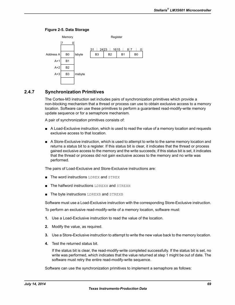
Figure 2-5. Data Storage
Memory Register
Address A
A+1
lsbyte
msbyte
A+2
A+3
07
B0B1B3 B231 2423 1615 8 7 0
B0
B1
B2
B3
2.4.7 Synchronization PrimitivesThe Cortex-M3 instruction set includes pairs of synchronization primitives which provide anon-blocking mechanism that a thread or process can use to obtain exclusive access to a memorylocation. Software can use these primitives to perform a guaranteed read-modify-write memoryupdate sequence or for a semaphore mechanism.
A pair of synchronization primitives consists of:
A Load-Exclusive instruction, which is used to read the value of a memory location and requestsexclusive access to that location.
A Store-Exclusive instruction, which is used to attempt to write to the same memory location andreturns a status bit to a register. If this status bit is clear, it indicates that the thread or processgained exclusive access to the memory and the write succeeds; if this status bit is set, it indicatesthat the thread or process did not gain exclusive access to the memory and no write wasperformed.
The pairs of Load-Exclusive and Store-Exclusive instructions are:
The word instructions LDREX and STREX
The halfword instructions LDREXH and STREXH
The byte instructions LDREXB and STREXB
Software must use a Load-Exclusive instruction with the corresponding Store-Exclusive instruction.
To perform an exclusive read-modify-write of a memory location, software must:
1. Use a Load-Exclusive instruction to read the value of the location.
2. Modify the value, as required.
3. Use a Store-Exclusive instruction to attempt to write the new value back to the memory location.
4. Test the returned status bit.
If the status bit is clear, the read-modify-write completed successfully. If the status bit is set, nowrite was performed, which indicates that the value returned at step 1 might be out of date. Thesoftware must retry the entire read-modify-write sequence.
Software can use the synchronization primitives to implement a semaphore as follows:
69July 14, 2014Texas Instruments-Production Data
Stellaris® LM3S601 Microcontroller
1. Use a Load-Exclusive instruction to read from the semaphore address to check whether thesemaphore is free.
2. If the semaphore is free, use a Store-Exclusive to write the claim value to the semaphoreaddress.
3. If the returned status bit from step 2 indicates that the Store-Exclusive succeeded, then thesoftware has claimed the semaphore. However, if the Store-Exclusive failed, another processmight have claimed the semaphore after the software performed step 1.
The Cortex-M3 includes an exclusive access monitor that tags the fact that the processor hasexecuted a Load-Exclusive instruction. The processor removes its exclusive access tag if:
It executes a CLREX instruction.
It executes a Store-Exclusive instruction, regardless of whether the write succeeds.
An exception occurs, which means the processor can resolve semaphore conflicts betweendifferent threads.
For more information about the synchronization primitive instructions, see the Cortex™-M3/M4Instruction Set Technical User's Manual.
2.5 Exception ModelThe ARM Cortex-M3 processor and the Nested Vectored Interrupt Controller (NVIC) prioritize andhandle all exceptions in Handler Mode. The processor state is automatically stored to the stack onan exception and automatically restored from the stack at the end of the Interrupt Service Routine(ISR). The vector is fetched in parallel to the state saving, enabling efficient interrupt entry. Theprocessor supports tail-chaining, which enables back-to-back interrupts to be performed without theoverhead of state saving and restoration.
Table 2-8 on page 72 lists all exception types. Software can set eight priority levels on seven ofthese exceptions (system handlers) as well as on 25 interrupts (listed in Table 2-9 on page 73).
Priorities on the system handlers are set with the NVIC System Handler Priority n (SYSPRIn)registers. Interrupts are enabled through the NVIC Interrupt Set Enable n (ENn) register andprioritized with the NVIC Interrupt Priority n (PRIn) registers. Priorities can be grouped by splittingpriority levels into preemption priorities and subpriorities. All the interrupt registers are described in“Nested Vectored Interrupt Controller (NVIC)” on page 86.
Internally, the highest user-programmable priority (0) is treated as fourth priority, after a Reset,Non-Maskable Interrupt (NMI), and a Hard Fault, in that order. Note that 0 is the default priority forall the programmable priorities.
Important: After a write to clear an interrupt source, it may take several processor cycles for theNVIC to see the interrupt source de-assert. Thus if the interrupt clear is done as thelast action in an interrupt handler, it is possible for the interrupt handler to completewhile the NVIC sees the interrupt as still asserted, causing the interrupt handler to bere-entered errantly. This situation can be avoided by either clearing the interrupt sourceat the beginning of the interrupt handler or by performing a read or write after the writeto clear the interrupt source (and flush the write buffer).
See “Nested Vectored Interrupt Controller (NVIC)” on page 86 for more information on exceptionsand interrupts.
July 14, 201470Texas Instruments-Production Data
The Cortex-M3 Processor
2.5.1 Exception StatesEach exception is in one of the following states:
Inactive. The exception is not active and not pending.
Pending. The exception is waiting to be serviced by the processor. An interrupt request from aperipheral or from software can change the state of the corresponding interrupt to pending.
Active. An exception that is being serviced by the processor but has not completed.
Note: An exception handler can interrupt the execution of another exception handler. In thiscase, both exceptions are in the active state.
Active and Pending. The exception is being serviced by the processor, and there is a pendingexception from the same source.
2.5.2 Exception TypesThe exception types are:
Reset. Reset is invoked on power up or a warm reset. The exception model treats reset as aspecial form of exception. When reset is asserted, the operation of the processor stops, potentiallyat any point in an instruction. When reset is deasserted, execution restarts from the addressprovided by the reset entry in the vector table. Execution restarts as privileged execution inThread mode.
NMI. A non-maskable Interrupt (NMI) can be signaled using the NMI signal or triggered bysoftware using the Interrupt Control and State (INTCTRL) register. This exception has thehighest priority other than reset. NMI is permanently enabled and has a fixed priority of -2. NMIscannot be masked or prevented from activation by any other exception or preempted by anyexception other than reset.
Hard Fault. A hard fault is an exception that occurs because of an error during exceptionprocessing, or because an exception cannot be managed by any other exception mechanism.Hard faults have a fixed priority of -1, meaning they have higher priority than any exception withconfigurable priority.
Memory Management Fault. Amemory management fault is an exception that occurs becauseof a memory protection related fault, including access violation and no match. The MPU or thefixed memory protection constraints determine this fault, for both instruction and data memorytransactions. This fault is used to abort instruction accesses to Execute Never (XN) memoryregions, even if the MPU is disabled.
Bus Fault. A bus fault is an exception that occurs because of a memory-related fault for aninstruction or data memory transaction such as a prefetch fault or a memory access fault. Thisfault can be enabled or disabled.
Usage Fault. A usage fault is an exception that occurs because of a fault related to instructionexecution, such as:
– An undefined instruction
– An illegal unaligned access
– Invalid state on instruction execution
71July 14, 2014Texas Instruments-Production Data
Stellaris® LM3S601 Microcontroller
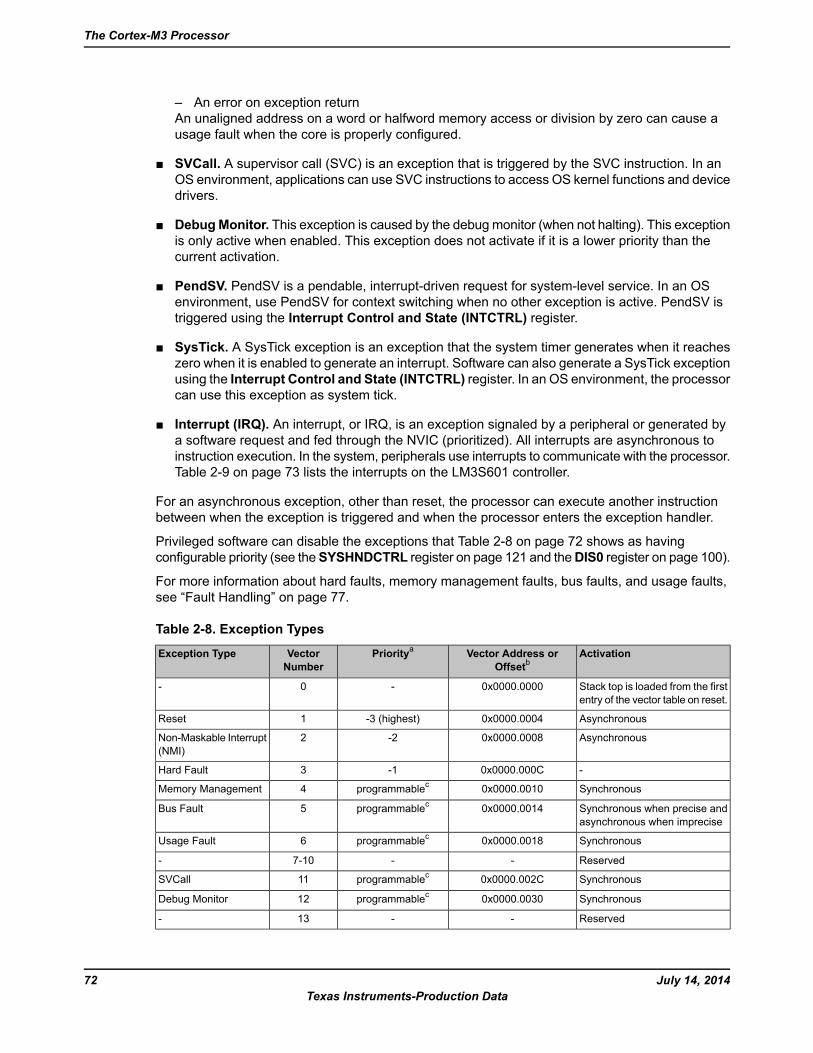
– An error on exception returnAn unaligned address on a word or halfword memory access or division by zero can cause ausage fault when the core is properly configured.
SVCall. A supervisor call (SVC) is an exception that is triggered by the SVC instruction. In anOS environment, applications can use SVC instructions to access OS kernel functions and devicedrivers.
DebugMonitor. This exception is caused by the debugmonitor (when not halting). This exceptionis only active when enabled. This exception does not activate if it is a lower priority than thecurrent activation.
PendSV. PendSV is a pendable, interrupt-driven request for system-level service. In an OSenvironment, use PendSV for context switching when no other exception is active. PendSV istriggered using the Interrupt Control and State (INTCTRL) register.
SysTick. A SysTick exception is an exception that the system timer generates when it reacheszero when it is enabled to generate an interrupt. Software can also generate a SysTick exceptionusing the Interrupt Control and State (INTCTRL) register. In an OS environment, the processorcan use this exception as system tick.
Interrupt (IRQ). An interrupt, or IRQ, is an exception signaled by a peripheral or generated bya software request and fed through the NVIC (prioritized). All interrupts are asynchronous toinstruction execution. In the system, peripherals use interrupts to communicate with the processor.Table 2-9 on page 73 lists the interrupts on the LM3S601 controller.
For an asynchronous exception, other than reset, the processor can execute another instructionbetween when the exception is triggered and when the processor enters the exception handler.
Privileged software can disable the exceptions that Table 2-8 on page 72 shows as havingconfigurable priority (see theSYSHNDCTRL register on page 121 and theDIS0 register on page 100).
For more information about hard faults, memory management faults, bus faults, and usage faults,see “Fault Handling” on page 77.
Table 2-8. Exception Types
ActivationVector Address orOffsetb
PriorityaVectorNumber
Exception Type
Stack top is loaded from the firstentry of the vector table on reset.
0x0000.0000-0-
Asynchronous0x0000.0004-3 (highest)1Reset
Asynchronous0x0000.0008-22Non-Maskable Interrupt(NMI)
-0x0000.000C-13Hard Fault
Synchronous0x0000.0010programmablec4Memory Management
Synchronous when precise andasynchronous when imprecise
0x0000.0014programmablec5Bus Fault
Synchronous0x0000.0018programmablec6Usage Fault
Reserved--7-10-
Synchronous0x0000.002Cprogrammablec11SVCall
Synchronous0x0000.0030programmablec12Debug Monitor
Reserved--13-
July 14, 201472Texas Instruments-Production Data
The Cortex-M3 Processor
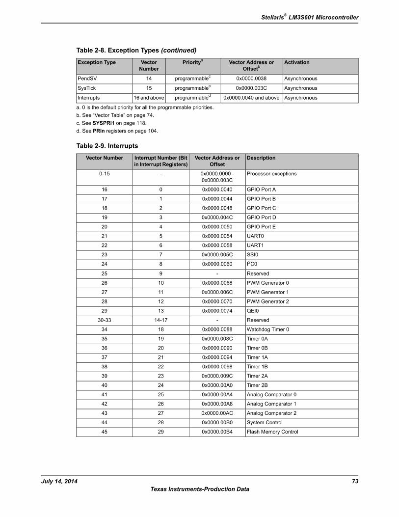
Table 2-8. Exception Types (continued)
ActivationVector Address orOffsetb
PriorityaVectorNumber
Exception Type
Asynchronous0x0000.0038programmablec14PendSV
Asynchronous0x0000.003Cprogrammablec15SysTick
Asynchronous0x0000.0040 and aboveprogrammabled16 and aboveInterrupts
a. 0 is the default priority for all the programmable priorities.b. See “Vector Table” on page 74.c. See SYSPRI1 on page 118.d. See PRIn registers on page 104.
Table 2-9. Interrupts
DescriptionVector Address orOffset
Interrupt Number (Bitin Interrupt Registers)
Vector Number
Processor exceptions0x0000.0000 -0x0000.003C
-0-15
GPIO Port A0x0000.0040016
GPIO Port B0x0000.0044117
GPIO Port C0x0000.0048218
GPIO Port D0x0000.004C319
GPIO Port E0x0000.0050420
UART00x0000.0054521
UART10x0000.0058622
SSI00x0000.005C723
I2C00x0000.0060824
Reserved-925
PWM Generator 00x0000.00681026
PWM Generator 10x0000.006C1127
PWM Generator 20x0000.00701228
QEI00x0000.00741329
Reserved-14-1730-33
Watchdog Timer 00x0000.00881834
Timer 0A0x0000.008C1935
Timer 0B0x0000.00902036
Timer 1A0x0000.00942137
Timer 1B0x0000.00982238
Timer 2A0x0000.009C2339
Timer 2B0x0000.00A02440
Analog Comparator 00x0000.00A42541
Analog Comparator 10x0000.00A82642
Analog Comparator 20x0000.00AC2743
System Control0x0000.00B02844
Flash Memory Control0x0000.00B42945
73July 14, 2014Texas Instruments-Production Data
Stellaris® LM3S601 Microcontroller
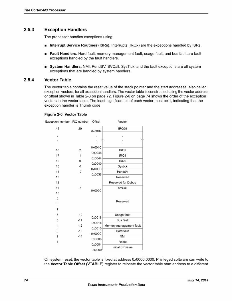
2.5.3 Exception HandlersThe processor handles exceptions using:
Interrupt Service Routines (ISRs). Interrupts (IRQx) are the exceptions handled by ISRs.
Fault Handlers. Hard fault, memory management fault, usage fault, and bus fault are faultexceptions handled by the fault handlers.
System Handlers. NMI, PendSV, SVCall, SysTick, and the fault exceptions are all systemexceptions that are handled by system handlers.
2.5.4 Vector TableThe vector table contains the reset value of the stack pointer and the start addresses, also calledexception vectors, for all exception handlers. The vector table is constructed using the vector addressor offset shown in Table 2-8 on page 72. Figure 2-6 on page 74 shows the order of the exceptionvectors in the vector table. The least-significant bit of each vector must be 1, indicating that theexception handler is Thumb code
Figure 2-6. Vector Table
Initial SP value
Reset
Hard fault
NMI
Memory management fault
Usage fault
Bus fault
0x0000
0x0004
0x0008
0x000C
0x0010
0x0014
0x0018
Reserved
SVCall
PendSV
Reserved for Debug
Systick
IRQ0
Reserved
0x002C
0x0038
0x003C
0x0040
OffsetException number
2
3
4
5
6
11
12
14
15
16
18
13
7
10
1
Vector
.
.
.
8
9
IRQ1
IRQ2
0x0044
IRQ29
170x0048
0x004C
45
.
.
.
.
.
.
0x00B4
IRQ number
-14
-13
-12
-11
-10
-5
-2
-1
0
2
1
29
On system reset, the vector table is fixed at address 0x0000.0000. Privileged software can write tothe Vector Table Offset (VTABLE) register to relocate the vector table start address to a different
July 14, 201474Texas Instruments-Production Data
The Cortex-M3 Processor
memory location, in the range 0x0000.0100 to 0x3FFF.FF00 (see “Vector Table” on page 74). Notethat when configuring the VTABLE register, the offset must be aligned on a 256-byte boundary.
2.5.5 Exception PrioritiesAs Table 2-8 on page 72 shows, all exceptions have an associated priority, with a lower priorityvalue indicating a higher priority and configurable priorities for all exceptions except Reset, Hardfault, and NMI. If software does not configure any priorities, then all exceptions with a configurablepriority have a priority of 0. For information about configuring exception priorities, see page 118 andpage 104.
Note: Configurable priority values for the Stellaris implementation are in the range 0-7. This meansthat the Reset, Hard fault, and NMI exceptions, with fixed negative priority values, alwayshave higher priority than any other exception.
For example, assigning a higher priority value to IRQ[0] and a lower priority value to IRQ[1] meansthat IRQ[1] has higher priority than IRQ[0]. If both IRQ[1] and IRQ[0] are asserted, IRQ[1] is processedbefore IRQ[0].
If multiple pending exceptions have the same priority, the pending exception with the lowest exceptionnumber takes precedence. For example, if both IRQ[0] and IRQ[1] are pending and have the samepriority, then IRQ[0] is processed before IRQ[1].
When the processor is executing an exception handler, the exception handler is preempted if ahigher priority exception occurs. If an exception occurs with the same priority as the exception beinghandled, the handler is not preempted, irrespective of the exception number. However, the statusof the new interrupt changes to pending.
2.5.6 Interrupt Priority GroupingTo increase priority control in systems with interrupts, the NVIC supports priority grouping. Thisgrouping divides each interrupt priority register entry into two fields:
An upper field that defines the group priority
A lower field that defines a subpriority within the group
Only the group priority determines preemption of interrupt exceptions. When the processor isexecuting an interrupt exception handler, another interrupt with the same group priority as theinterrupt being handled does not preempt the handler.
If multiple pending interrupts have the same group priority, the subpriority field determines the orderin which they are processed. If multiple pending interrupts have the same group priority andsubpriority, the interrupt with the lowest IRQ number is processed first.
For information about splitting the interrupt priority fields into group priority and subpriority, seepage 112.
2.5.7 Exception Entry and ReturnDescriptions of exception handling use the following terms:
Preemption.When the processor is executing an exception handler, an exception can preemptthe exception handler if its priority is higher than the priority of the exception being handled. See“Interrupt Priority Grouping” on page 75 for more information about preemption by an interrupt.When one exception preempts another, the exceptions are called nested exceptions. See“Exception Entry” on page 76 more information.
75July 14, 2014Texas Instruments-Production Data
Stellaris® LM3S601 Microcontroller
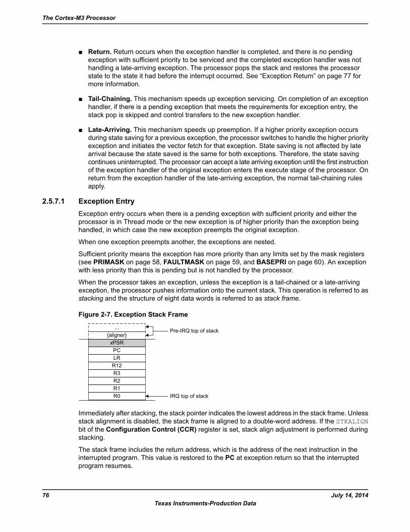
Return. Return occurs when the exception handler is completed, and there is no pendingexception with sufficient priority to be serviced and the completed exception handler was nothandling a late-arriving exception. The processor pops the stack and restores the processorstate to the state it had before the interrupt occurred. See “Exception Return” on page 77 formore information.
Tail-Chaining. This mechanism speeds up exception servicing. On completion of an exceptionhandler, if there is a pending exception that meets the requirements for exception entry, thestack pop is skipped and control transfers to the new exception handler.
Late-Arriving. This mechanism speeds up preemption. If a higher priority exception occursduring state saving for a previous exception, the processor switches to handle the higher priorityexception and initiates the vector fetch for that exception. State saving is not affected by latearrival because the state saved is the same for both exceptions. Therefore, the state savingcontinues uninterrupted. The processor can accept a late arriving exception until the first instructionof the exception handler of the original exception enters the execute stage of the processor. Onreturn from the exception handler of the late-arriving exception, the normal tail-chaining rulesapply.
2.5.7.1 Exception EntryException entry occurs when there is a pending exception with sufficient priority and either theprocessor is in Thread mode or the new exception is of higher priority than the exception beinghandled, in which case the new exception preempts the original exception.
When one exception preempts another, the exceptions are nested.
Sufficient priority means the exception has more priority than any limits set by the mask registers(see PRIMASK on page 58, FAULTMASK on page 59, and BASEPRI on page 60). An exceptionwith less priority than this is pending but is not handled by the processor.
When the processor takes an exception, unless the exception is a tail-chained or a late-arrivingexception, the processor pushes information onto the current stack. This operation is referred to asstacking and the structure of eight data words is referred to as stack frame.
Figure 2-7. Exception Stack Frame
Pre-IRQ top of stack
xPSRPCLRR12R3R2R1R0
aligner
IRQ top of stack
...
Immediately after stacking, the stack pointer indicates the lowest address in the stack frame. Unlessstack alignment is disabled, the stack frame is aligned to a double-word address. If the STKALIGNbit of the Configuration Control (CCR) register is set, stack align adjustment is performed duringstacking.
The stack frame includes the return address, which is the address of the next instruction in theinterrupted program. This value is restored to the PC at exception return so that the interruptedprogram resumes.
July 14, 201476Texas Instruments-Production Data
The Cortex-M3 Processor
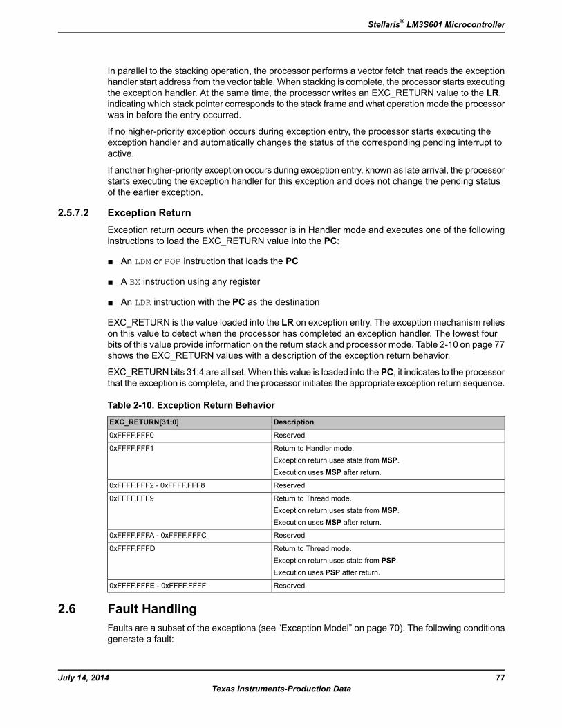
In parallel to the stacking operation, the processor performs a vector fetch that reads the exceptionhandler start address from the vector table. When stacking is complete, the processor starts executingthe exception handler. At the same time, the processor writes an EXC_RETURN value to the LR,indicating which stack pointer corresponds to the stack frame and what operation mode the processorwas in before the entry occurred.
If no higher-priority exception occurs during exception entry, the processor starts executing theexception handler and automatically changes the status of the corresponding pending interrupt toactive.
If another higher-priority exception occurs during exception entry, known as late arrival, the processorstarts executing the exception handler for this exception and does not change the pending statusof the earlier exception.
2.5.7.2 Exception ReturnException return occurs when the processor is in Handler mode and executes one of the followinginstructions to load the EXC_RETURN value into the PC:
An LDM or POP instruction that loads the PC
A BX instruction using any register
An LDR instruction with the PC as the destination
EXC_RETURN is the value loaded into the LR on exception entry. The exception mechanism relieson this value to detect when the processor has completed an exception handler. The lowest fourbits of this value provide information on the return stack and processor mode. Table 2-10 on page 77shows the EXC_RETURN values with a description of the exception return behavior.
EXC_RETURN bits 31:4 are all set. When this value is loaded into thePC, it indicates to the processorthat the exception is complete, and the processor initiates the appropriate exception return sequence.
Table 2-10. Exception Return Behavior
DescriptionEXC_RETURN[31:0]
Reserved0xFFFF.FFF0
Return to Handler mode.Exception return uses state from MSP.Execution uses MSP after return.
0xFFFF.FFF1
Reserved0xFFFF.FFF2 - 0xFFFF.FFF8
Return to Thread mode.Exception return uses state from MSP.Execution uses MSP after return.
0xFFFF.FFF9
Reserved0xFFFF.FFFA - 0xFFFF.FFFC
Return to Thread mode.Exception return uses state from PSP.Execution uses PSP after return.
0xFFFF.FFFD
Reserved0xFFFF.FFFE - 0xFFFF.FFFF
2.6 Fault HandlingFaults are a subset of the exceptions (see “Exception Model” on page 70). The following conditionsgenerate a fault:
77July 14, 2014Texas Instruments-Production Data
Stellaris® LM3S601 Microcontroller
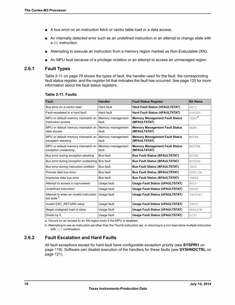
A bus error on an instruction fetch or vector table load or a data access.
An internally detected error such as an undefined instruction or an attempt to change state witha BX instruction.
Attempting to execute an instruction from a memory region marked as Non-Executable (XN).
An MPU fault because of a privilege violation or an attempt to access an unmanaged region.
2.6.1 Fault TypesTable 2-11 on page 78 shows the types of fault, the handler used for the fault, the correspondingfault status register, and the register bit that indicates the fault has occurred. See page 125 for moreinformation about the fault status registers.
Table 2-11. Faults
Bit NameFault Status RegisterHandlerFault
VECTHard Fault Status (HFAULTSTAT)Hard faultBus error on a vector read
FORCEDHard Fault Status (HFAULTSTAT)Hard faultFault escalated to a hard fault
IERR aMemory Management Fault Status(MFAULTSTAT)
Memory managementfault
MPU or default memory mismatch oninstruction access
DERRMemory Management Fault Status(MFAULTSTAT)
Memory managementfault
MPU or default memory mismatch ondata access
MSTKEMemory Management Fault Status(MFAULTSTAT)
Memory managementfault
MPU or default memory mismatch onexception stacking
MUSTKEMemory Management Fault Status(MFAULTSTAT)
Memory managementfault
MPU or default memory mismatch onexception unstacking
BSTKEBus Fault Status (BFAULTSTAT)Bus faultBus error during exception stacking
BUSTKEBus Fault Status (BFAULTSTAT)Bus faultBus error during exception unstacking
IBUSBus Fault Status (BFAULTSTAT)Bus faultBus error during instruction prefetch
PRECISEBus Fault Status (BFAULTSTAT)Bus faultPrecise data bus error
IMPREBus Fault Status (BFAULTSTAT)Bus faultImprecise data bus error
NOCPUsage Fault Status (UFAULTSTAT)Usage faultAttempt to access a coprocessor
UNDEFUsage Fault Status (UFAULTSTAT)Usage faultUndefined instruction
INVSTATUsage Fault Status (UFAULTSTAT)Usage faultAttempt to enter an invalid instructionset state b
INVPCUsage Fault Status (UFAULTSTAT)Usage faultInvalid EXC_RETURN value
UNALIGNUsage Fault Status (UFAULTSTAT)Usage faultIllegal unaligned load or store
DIV0Usage Fault Status (UFAULTSTAT)Usage faultDivide by 0
a. Occurs on an access to an XN region even if the MPU is disabled.b. Attempting to use an instruction set other than the Thumb instruction set, or returning to a non load-store-multiple instruction
with ICI continuation.
2.6.2 Fault Escalation and Hard FaultsAll fault exceptions except for hard fault have configurable exception priority (see SYSPRI1 onpage 118). Software can disable execution of the handlers for these faults (see SYSHNDCTRL onpage 121).
July 14, 201478Texas Instruments-Production Data
The Cortex-M3 Processor
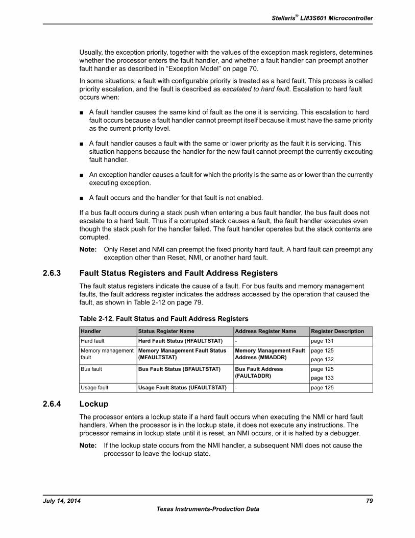
Usually, the exception priority, together with the values of the exception mask registers, determineswhether the processor enters the fault handler, and whether a fault handler can preempt anotherfault handler as described in “Exception Model” on page 70.
In some situations, a fault with configurable priority is treated as a hard fault. This process is calledpriority escalation, and the fault is described as escalated to hard fault. Escalation to hard faultoccurs when:
A fault handler causes the same kind of fault as the one it is servicing. This escalation to hardfault occurs because a fault handler cannot preempt itself because it must have the same priorityas the current priority level.
A fault handler causes a fault with the same or lower priority as the fault it is servicing. Thissituation happens because the handler for the new fault cannot preempt the currently executingfault handler.
An exception handler causes a fault for which the priority is the same as or lower than the currentlyexecuting exception.
A fault occurs and the handler for that fault is not enabled.
If a bus fault occurs during a stack push when entering a bus fault handler, the bus fault does notescalate to a hard fault. Thus if a corrupted stack causes a fault, the fault handler executes eventhough the stack push for the handler failed. The fault handler operates but the stack contents arecorrupted.
Note: Only Reset and NMI can preempt the fixed priority hard fault. A hard fault can preempt anyexception other than Reset, NMI, or another hard fault.
2.6.3 Fault Status Registers and Fault Address RegistersThe fault status registers indicate the cause of a fault. For bus faults and memory managementfaults, the fault address register indicates the address accessed by the operation that caused thefault, as shown in Table 2-12 on page 79.
Table 2-12. Fault Status and Fault Address Registers
Register DescriptionAddress Register NameStatus Register NameHandler
page 131-Hard Fault Status (HFAULTSTAT)Hard fault
page 125page 132
Memory Management FaultAddress (MMADDR)
Memory Management Fault Status(MFAULTSTAT)
Memory managementfault
page 125page 133
Bus Fault Address(FAULTADDR)
Bus Fault Status (BFAULTSTAT)Bus fault
page 125-Usage Fault Status (UFAULTSTAT)Usage fault
2.6.4 LockupThe processor enters a lockup state if a hard fault occurs when executing the NMI or hard faulthandlers. When the processor is in the lockup state, it does not execute any instructions. Theprocessor remains in lockup state until it is reset, an NMI occurs, or it is halted by a debugger.
Note: If the lockup state occurs from the NMI handler, a subsequent NMI does not cause theprocessor to leave the lockup state.
79July 14, 2014Texas Instruments-Production Data
Stellaris® LM3S601 Microcontroller
2.7 Power ManagementThe Cortex-M3 processor sleep modes reduce power consumption:
Sleep mode stops the processor clock.
Deep-sleep mode stops the system clock and switches off the PLL and Flash memory.
The SLEEPDEEP bit of the System Control (SYSCTRL) register selects which sleep mode is used(see page 114). For more information about the behavior of the sleep modes, see “SystemControl” on page 161.
This section describes the mechanisms for entering sleep mode and the conditions for waking upfrom sleep mode, both of which apply to Sleep mode and Deep-sleep mode.
2.7.1 Entering Sleep ModesThis section describes the mechanisms software can use to put the processor into one of the sleepmodes.
The system can generate spurious wake-up events, for example a debug operation wakes up theprocessor. Therefore, software must be able to put the processor back into sleep mode after suchan event. A program might have an idle loop to put the processor back to sleep mode.
2.7.1.1 Wait for InterruptThe wait for interrupt instruction, WFI, causes immediate entry to sleep mode unless the wake-upcondition is true (see “Wake Up from WFI or Sleep-on-Exit” on page 81). When the processorexecutes a WFI instruction, it stops executing instructions and enters sleep mode. See theCortex™-M3/M4 Instruction Set Technical User's Manual for more information.
2.7.1.2 Wait for EventThe wait for event instruction, WFE, causes entry to sleep mode conditional on the value of a one-bitevent register. When the processor executes a WFE instruction, it checks the event register. If theregister is 0, the processor stops executing instructions and enters sleep mode. If the register is 1,the processor clears the register and continues executing instructions without entering sleep mode.
If the event register is 1, the processor must not enter sleep mode on execution of a WFE instruction.Typically, this situation occurs if an SEV instruction has been executed. Software cannot accessthis register directly.
See the Cortex™-M3/M4 Instruction Set Technical User's Manual for more information.
2.7.1.3 Sleep-on-ExitIf the SLEEPEXIT bit of the SYSCTRL register is set, when the processor completes the executionof all exception handlers, it returns to Thread mode and immediately enters sleep mode. Thismechanism can be used in applications that only require the processor to run when an exceptionoccurs.
2.7.2 Wake Up from Sleep ModeThe conditions for the processor to wake up depend on the mechanism that cause it to enter sleepmode.
July 14, 201480Texas Instruments-Production Data
The Cortex-M3 Processor
2.7.2.1 Wake Up from WFI or Sleep-on-ExitNormally, the processor wakes up only when the NVIC detects an exception with sufficient priorityto cause exception entry. Some embedded systems might have to execute system restore tasksafter the processor wakes up and before executing an interrupt handler. Entry to the interrupt handlercan be delayed by setting the PRIMASK bit and clearing the FAULTMASK bit. If an interrupt arrivesthat is enabled and has a higher priority than current exception priority, the processor wakes up butdoes not execute the interrupt handler until the processor clears PRIMASK. For more informationabout PRIMASK and FAULTMASK, see page 58 and page 59.
2.7.2.2 Wake Up from WFEThe processor wakes up if it detects an exception with sufficient priority to cause exception entry.
In addition, if the SEVONPEND bit in the SYSCTRL register is set, any new pending interrupt triggersan event and wakes up the processor, even if the interrupt is disabled or has insufficient priority tocause exception entry. For more information about SYSCTRL, see page 114.
2.8 Instruction Set SummaryThe processor implements a version of the Thumb instruction set. Table 2-13 on page 81 lists thesupported instructions.
Note: In Table 2-13 on page 81:
Angle brackets, <>, enclose alternative forms of the operand Braces, , enclose optional operands The Operands column is not exhaustive Op2 is a flexible second operand that can be either a register or a constant Most instructions can use an optional condition code suffix
For more information on the instructions and operands, see the instruction descriptions inthe Cortex™-M3/M4 Instruction Set Technical User's Manual.
Table 2-13. Cortex-M3 Instruction Summary
FlagsBrief DescriptionOperandsMnemonic
N,Z,C,VAdd with carryRd, Rn, Op2ADC, ADCS
N,Z,C,VAddRd, Rn, Op2ADD, ADDS
N,Z,C,VAddRd, Rn , #imm12ADD, ADDW
-Load PC-relative addressRd, labelADR
N,Z,CLogical ANDRd, Rn, Op2AND, ANDS
N,Z,CArithmetic shift rightRd, Rm, <Rs|#n>ASR, ASRS
-BranchlabelB
-Bit field clearRd, #lsb, #widthBFC
-Bit field insertRd, Rn, #lsb, #widthBFI
N,Z,CBit clearRd, Rn, Op2BIC, BICS
-Breakpoint#immBKPT
-Branch with linklabelBL
-Branch indirect with linkRmBLX
-Branch indirectRmBX
-Compare and branch if non-zeroRn, labelCBNZ
81July 14, 2014Texas Instruments-Production Data
Stellaris® LM3S601 Microcontroller
Table 2-13. Cortex-M3 Instruction Summary (continued)
FlagsBrief DescriptionOperandsMnemonic
-Compare and branch if zeroRn, labelCBZ
-Clear exclusive-CLREX
-Count leading zerosRd, RmCLZ
N,Z,C,VCompare negativeRn, Op2CMN
N,Z,C,VCompareRn, Op2CMP
-Change processor state, disableinterrupts
iCPSID
-Change processor state, enableinterrupts
iCPSIE
-Data memory barrier-DMB
-Data synchronization barrier-DSB
N,Z,CExclusive ORRd, Rn, Op2EOR, EORS
-Instruction synchronization barrier-ISB
-If-Then condition block-IT
-Load multiple registers, increment afterRn!, reglistLDM
-Load multiple registers, decrementbefore
Rn!, reglistLDMDB, LDMEA
-Load multiple registers, increment afterRn!, reglistLDMFD, LDMIA
-Load register with wordRt, [Rn, #offset]LDR
-Load register with byteRt, [Rn, #offset]LDRB, LDRBT
-Load register with two bytesRt, Rt2, [Rn, #offset]LDRD
-Load register exclusiveRt, [Rn, #offset]LDREX
-Load register exclusive with byteRt, [Rn]LDREXB
-Load register exclusive with halfwordRt, [Rn]LDREXH
-Load register with halfwordRt, [Rn, #offset]LDRH, LDRHT
-Load register with signed byteRt, [Rn, #offset]LDRSB, LDRSBT
-Load register with signed halfwordRt, [Rn, #offset]LDRSH, LDRSHT
-Load register with wordRt, [Rn, #offset]LDRT
N,Z,CLogical shift leftRd, Rm, <Rs|#n>LSL, LSLS
N,Z,CLogical shift rightRd, Rm, <Rs|#n>LSR, LSRS
-Multiply with accumulate, 32-bit resultRd, Rn, Rm, RaMLA
-Multiply and subtract, 32-bit resultRd, Rn, Rm, RaMLS
N,Z,CMoveRd, Op2MOV, MOVS
N,Z,CMove 16-bit constantRd, #imm16MOV, MOVW
-Move topRd, #imm16MOVT
-Move from special register to generalregister
Rd, spec_regMRS
N,Z,C,VMove from general register to specialregister
spec_reg, RmMSR
N,ZMultiply, 32-bit resultRd, Rn, RmMUL, MULS
N,Z,CMove NOTRd, Op2MVN, MVNS
-No operation-NOP
N,Z,CLogical OR NOTRd, Rn, Op2ORN, ORNS
July 14, 201482Texas Instruments-Production Data
The Cortex-M3 Processor
Table 2-13. Cortex-M3 Instruction Summary (continued)
FlagsBrief DescriptionOperandsMnemonic
N,Z,CLogical ORRd, Rn, Op2ORR, ORRS
-Pop registers from stackreglistPOP
-Push registers onto stackreglistPUSH
-Reverse bitsRd, RnRBIT
-Reverse byte order in a wordRd, RnREV
-Reverse byte order in each halfwordRd, RnREV16
-Reverse byte order in bottom halfwordand sign extend
Rd, RnREVSH
N,Z,CRotate rightRd, Rm, <Rs|#n>ROR, RORS
N,Z,CRotate right with extendRd, RmRRX, RRXS
N,Z,C,VReverse subtractRd, Rn, Op2RSB, RSBS
N,Z,C,VSubtract with carryRd, Rn, Op2SBC, SBCS
-Signed bit field extractRd, Rn, #lsb, #widthSBFX
-Signed divideRd, Rn, RmSDIV
-Send event-SEV
-Signed multiply with accumulate(32x32+64), 64-bit result
RdLo, RdHi, Rn, RmSMLAL
-Signed multiply (32x32), 64-bit resultRdLo, RdHi, Rn, RmSMULL
QSigned saturateRd, #n, Rm ,shift #sSSAT
-Store multiple registers, increment afterRn!, reglistSTM
-Store multiple registers, decrementbefore
Rn!, reglistSTMDB, STMEA
-Store multiple registers, increment afterRn!, reglistSTMFD, STMIA
-Store register wordRt, [Rn , #offset]STR
-Store register byteRt, [Rn , #offset]STRB, STRBT
-Store register two wordsRt, Rt2, [Rn , #offset]STRD
-Store register exclusiveRt, Rt, [Rn , #offset]STREX
-Store register exclusive byteRd, Rt, [Rn]STREXB
-Store register exclusive halfwordRd, Rt, [Rn]STREXH
-Store register halfwordRt, [Rn , #offset]STRH, STRHT
-Store register signed byteRt, [Rn , #offset]STRSB, STRSBT
-Store register signed halfwordRt, [Rn , #offset]STRSH, STRSHT
-Store register wordRt, [Rn , #offset]STRT
N,Z,C,VSubtractRd, Rn, Op2SUB, SUBS
N,Z,C,VSubtract 12-bit constantRd, Rn, #imm12SUB, SUBW
-Supervisor call#immSVC
-Sign extend a byteRd, Rm ,ROR #nSXTB
-Sign extend a halfwordRd, Rm ,ROR #nSXTH
-Table branch byte[Rn, Rm]TBB
-Table branch halfword[Rn, Rm, LSL #1]TBH
N,Z,CTest equivalenceRn, Op2TEQ
N,Z,CTestRn, Op2TST
83July 14, 2014Texas Instruments-Production Data
Stellaris® LM3S601 Microcontroller
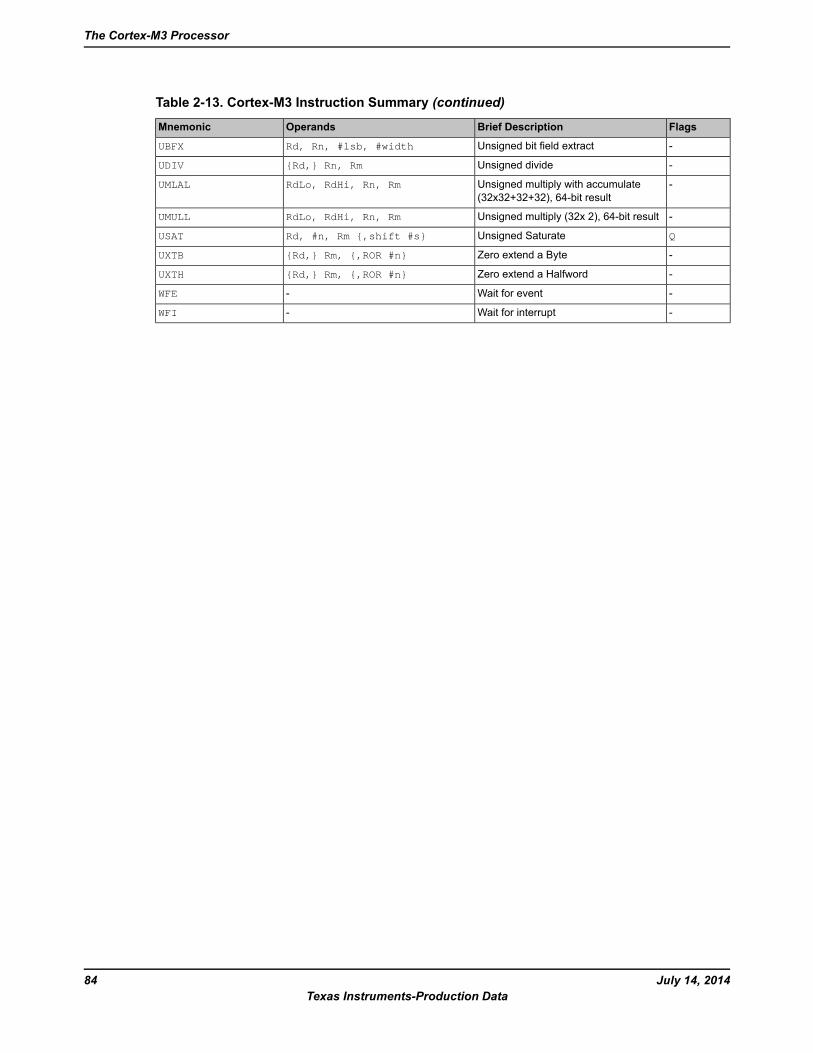
Table 2-13. Cortex-M3 Instruction Summary (continued)
FlagsBrief DescriptionOperandsMnemonic
-Unsigned bit field extractRd, Rn, #lsb, #widthUBFX
-Unsigned divideRd, Rn, RmUDIV
-Unsigned multiply with accumulate(32x32+32+32), 64-bit result
RdLo, RdHi, Rn, RmUMLAL
-Unsigned multiply (32x 2), 64-bit resultRdLo, RdHi, Rn, RmUMULL
QUnsigned SaturateRd, #n, Rm ,shift #sUSAT
-Zero extend a ByteRd, Rm, ,ROR #nUXTB
-Zero extend a HalfwordRd, Rm, ,ROR #nUXTH
-Wait for event-WFE
-Wait for interrupt-WFI
July 14, 201484Texas Instruments-Production Data
The Cortex-M3 Processor
3 Cortex-M3 PeripheralsThis chapter provides information on the Stellaris® implementation of the Cortex-M3 processorperipherals, including:
SysTick (see page 85)
Provides a simple, 24-bit clear-on-write, decrementing, wrap-on-zero counter with a flexiblecontrol mechanism.
Nested Vectored Interrupt Controller (NVIC) (see page 86)– Facilitates low-latency exception and interrupt handling– Controls power management– Implements system control registers
System Control Block (SCB) (see page 88)
Provides system implementation information and system control, including configuration, control,and reporting of system exceptions.
Memory Protection Unit (MPU) (see page 88)
Supports the standard ARMv7 ProtectedMemory System Architecture (PMSA)model. TheMPUprovides full support for protection regions, overlapping protection regions, access permissions,and exporting memory attributes to the system.
Table 3-1 on page 85 shows the address map of the Private Peripheral Bus (PPB). Some peripheralregister regions are split into two address regions, as indicated by two addresses listed.
Table 3-1. Core Peripheral Register Regions
Description (see page ...)Core PeripheralAddress
85System Timer0xE000.E010-0xE000.E01F
86Nested Vectored Interrupt Controller0xE000.E100-0xE000.E4EF0xE000.EF00-0xE000.EF03
88System Control Block0xE000.ED00-0xE000.ED3F
88Memory Protection Unit0xE000.ED90-0xE000.EDB8
3.1 Functional DescriptionThis chapter provides information on the Stellaris implementation of the Cortex-M3 processorperipherals: SysTick, NVIC, SCB and MPU.
3.1.1 System Timer (SysTick)Cortex-M3 includes an integrated system timer, SysTick, which provides a simple, 24-bitclear-on-write, decrementing, wrap-on-zero counter with a flexible control mechanism. The countercan be used in several different ways, for example as:
An RTOS tick timer that fires at a programmable rate (for example, 100 Hz) and invokes a SysTickroutine.
A high-speed alarm timer using the system clock.
85July 14, 2014Texas Instruments-Production Data
Stellaris® LM3S601 Microcontroller
A variable rate alarm or signal timer—the duration is range-dependent on the reference clockused and the dynamic range of the counter.
A simple counter used to measure time to completion and time used.
An internal clock source control based on missing/meeting durations. The COUNT bit in theSTCTRL control and status register can be used to determine if an action completed within aset duration, as part of a dynamic clock management control loop.
The timer consists of three registers:
SysTick Control and Status (STCTRL): A control and status counter to configure its clock,enable the counter, enable the SysTick interrupt, and determine counter status.
SysTick Reload Value (STRELOAD): The reload value for the counter, used to provide thecounter's wrap value.
SysTick Current Value (STCURRENT): The current value of the counter.
When enabled, the timer counts down on each clock from the reload value to zero, reloads (wraps)to the value in the STRELOAD register on the next clock edge, then decrements on subsequentclocks. Clearing the STRELOAD register disables the counter on the next wrap. When the counterreaches zero, the COUNT status bit is set. The COUNT bit clears on reads.
Writing to the STCURRENT register clears the register and the COUNT status bit. The write doesnot trigger the SysTick exception logic. On a read, the current value is the value of the register atthe time the register is accessed.
The SysTick counter runs on the system clock. If this clock signal is stopped for low power mode,the SysTick counter stops. Ensure software uses aligned word accesses to access the SysTickregisters.
Note: When the processor is halted for debugging, the counter does not decrement.
3.1.2 Nested Vectored Interrupt Controller (NVIC)This section describes the Nested Vectored Interrupt Controller (NVIC) and the registers it uses.The NVIC supports:
25 interrupts.
A programmable priority level of 0-7 for each interrupt. A higher level corresponds to a lowerpriority, so level 0 is the highest interrupt priority.
Low-latency exception and interrupt handling.
Level and pulse detection of interrupt signals.
Dynamic reprioritization of interrupts.
Grouping of priority values into group priority and subpriority fields.
Interrupt tail-chaining.
An external Non-maskable interrupt (NMI).
July 14, 201486Texas Instruments-Production Data
Cortex-M3 Peripherals
The processor automatically stacks its state on exception entry and unstacks this state on exceptionexit, with no instruction overhead, providing low latency exception handling.
3.1.2.1 Level-Sensitive and Pulse InterruptsThe processor supports both level-sensitive and pulse interrupts. Pulse interrupts are also describedas edge-triggered interrupts.
A level-sensitive interrupt is held asserted until the peripheral deasserts the interrupt signal. Typicallythis happens because the ISR accesses the peripheral, causing it to clear the interrupt request. Apulse interrupt is an interrupt signal sampled synchronously on the rising edge of the processorclock. To ensure the NVIC detects the interrupt, the peripheral must assert the interrupt signal forat least one clock cycle, during which the NVIC detects the pulse and latches the interrupt.
When the processor enters the ISR, it automatically removes the pending state from the interrupt(see “Hardware and Software Control of Interrupts” on page 87 for more information). For alevel-sensitive interrupt, if the signal is not deasserted before the processor returns from the ISR,the interrupt becomes pending again, and the processor must execute its ISR again. As a result,the peripheral can hold the interrupt signal asserted until it no longer needs servicing.
3.1.2.2 Hardware and Software Control of InterruptsThe Cortex-M3 latches all interrupts. A peripheral interrupt becomes pending for one of the followingreasons:
The NVIC detects that the interrupt signal is High and the interrupt is not active.
The NVIC detects a rising edge on the interrupt signal.
Software writes to the corresponding interrupt set-pending register bit, or to the Software TriggerInterrupt (SWTRIG) register to make a Software-Generated Interrupt pending. See the INT bitin the PEND0 register on page 101 or SWTRIG on page 106.
A pending interrupt remains pending until one of the following:
The processor enters the ISR for the interrupt, changing the state of the interrupt from pendingto active. Then:
– For a level-sensitive interrupt, when the processor returns from the ISR, the NVIC samplesthe interrupt signal. If the signal is asserted, the state of the interrupt changes to pending,which might cause the processor to immediately re-enter the ISR. Otherwise, the state of theinterrupt changes to inactive.
– For a pulse interrupt, the NVIC continues to monitor the interrupt signal, and if this is pulsedthe state of the interrupt changes to pending and active. In this case, when the processorreturns from the ISR the state of the interrupt changes to pending, which might cause theprocessor to immediately re-enter the ISR.
If the interrupt signal is not pulsed while the processor is in the ISR, when the processorreturns from the ISR the state of the interrupt changes to inactive.
Software writes to the corresponding interrupt clear-pending register bit
– For a level-sensitive interrupt, if the interrupt signal is still asserted, the state of the interruptdoes not change. Otherwise, the state of the interrupt changes to inactive.
87July 14, 2014Texas Instruments-Production Data
Stellaris® LM3S601 Microcontroller
– For a pulse interrupt, the state of the interrupt changes to inactive, if the state was pendingor to active, if the state was active and pending.
3.1.3 System Control Block (SCB)The System Control Block (SCB) provides system implementation information and system control,including configuration, control, and reporting of the system exceptions.
3.1.4 Memory Protection Unit (MPU)This section describes the Memory protection unit (MPU). The MPU divides the memory map intoa number of regions and defines the location, size, access permissions, and memory attributes ofeach region. The MPU supports independent attribute settings for each region, overlapping regions,and export of memory attributes to the system.
The memory attributes affect the behavior of memory accesses to the region. The Cortex-M3 MPUdefines eight separate memory regions, 0-7, and a background region.
When memory regions overlap, a memory access is affected by the attributes of the region with thehighest number. For example, the attributes for region 7 take precedence over the attributes of anyregion that overlaps region 7.
The background region has the same memory access attributes as the default memory map, but isaccessible from privileged software only.
The Cortex-M3 MPU memory map is unified, meaning that instruction accesses and data accesseshave the same region settings.
If a program accesses a memory location that is prohibited by the MPU, the processor generatesa memory management fault, causing a fault exception and possibly causing termination of theprocess in an OS environment. In an OS environment, the kernel can update the MPU region settingdynamically based on the process to be executed. Typically, an embedded OS uses the MPU formemory protection.
Configuration of MPU regions is based on memory types (see “Memory Regions, Types andAttributes” on page 63 for more information).
Table 3-2 on page 88 shows the possible MPU region attributes. See the section called “MPUConfiguration for a Stellaris Microcontroller” on page 92 for guidelines for programming amicrocontroller implementation.
Table 3-2. Memory Attributes Summary
DescriptionMemory Type
All accesses to Strongly Ordered memory occur in program order.Strongly Ordered
Memory-mapped peripheralsDevice
Normal memoryNormal
To avoid unexpected behavior, disable the interrupts before updating the attributes of a region thatthe interrupt handlers might access.
Ensure software uses aligned accesses of the correct size to access MPU registers:
Except for the MPU Region Attribute and Size (MPUATTR) register, all MPU registers mustbe accessed with aligned word accesses.
The MPUATTR register can be accessed with byte or aligned halfword or word accesses.
July 14, 201488Texas Instruments-Production Data
Cortex-M3 Peripherals
The processor does not support unaligned accesses to MPU registers.
When setting up the MPU, and if the MPU has previously been programmed, disable unused regionsto prevent any previous region settings from affecting the new MPU setup.
3.1.4.1 Updating an MPU RegionTo update the attributes for an MPU region, the MPU Region Number (MPUNUMBER), MPURegion Base Address (MPUBASE) and MPUATTR registers must be updated. Each register canbe programmed separately or with a multiple-word write to program all of these registers. You canuse the MPUBASEx and MPUATTRx aliases to program up to four regions simultaneously usingan STM instruction.
Updating an MPU Region Using Separate Words
This example simple code configures one region:
; R1 = region number; R2 = size/enable; R3 = attributes; R4 = address LDR R0,=MPUNUMBER ; 0xE000ED98, MPU region number register STR R1, [R0, #0x0] ; Region NumberSTR R4, [R0, #0x4] ; Region Base AddressSTRH R2, [R0, #0x8] ; Region Size and EnableSTRH R3, [R0, #0xA] ; Region Attribute
Disable a region before writing new region settings to the MPU if you have previously enabled theregion being changed. For example:
; R1 = region number; R2 = size/enable; R3 = attributes; R4 = addressLDR R0,=MPUNUMBER ; 0xE000ED98, MPU region number registerSTR R1, [R0, #0x0] ; Region NumberBIC R2, R2, #1 ; DisableSTRH R2, [R0, #0x8] ; Region Size and EnableSTR R4, [R0, #0x4] ; Region Base AddressSTRH R3, [R0, #0xA] ; Region AttributeORR R2, #1 ; EnableSTRH R2, [R0, #0x8] ; Region Size and Enable
Software must use memory barrier instructions:
Before MPU setup, if there might be outstanding memory transfers, such as buffered writes, thatmight be affected by the change in MPU settings.
After MPU setup, if it includes memory transfers that must use the new MPU settings.
However, memory barrier instructions are not required if the MPU setup process starts by enteringan exception handler, or is followed by an exception return, because the exception entry andexception return mechanism cause memory barrier behavior.
Software does not need any memory barrier instructions during MPU setup, because it accessesthe MPU through the Private Peripheral Bus (PPB), which is a Strongly Ordered memory region.
89July 14, 2014Texas Instruments-Production Data
Stellaris® LM3S601 Microcontroller
For example, if all of the memory access behavior is intended to take effect immediately after theprogramming sequence, then a DSB instruction and an ISB instruction should be used. A DSB isrequired after changing MPU settings, such as at the end of context switch. An ISB is required ifthe code that programs the MPU region or regions is entered using a branch or call. If theprogramming sequence is entered using a return from exception, or by taking an exception, thenan ISB is not required.
Updating an MPU Region Using Multi-Word Writes
The MPU can be programmed directly using multi-word writes, depending how the information isdivided. Consider the following reprogramming:
; R1 = region number; R2 = address; R3 = size, attributes in oneLDR R0, =MPUNUMBER ; 0xE000ED98, MPU region number registerSTR R1, [R0, #0x0] ; Region NumberSTR R2, [R0, #0x4] ; Region Base AddressSTR R3, [R0, #0x8] ; Region Attribute, Size and Enable
An STM instruction can be used to optimize this:
; R1 = region number; R2 = address; R3 = size, attributes in oneLDR R0, =MPUNUMBER ; 0xE000ED98, MPU region number registerSTM R0, R1-R3 ; Region number, address, attribute, size and enable
This operation can be done in two words for pre-packed information, meaning that theMPU RegionBase Address (MPUBASE) register (see page 138) contains the required region number and hasthe VALID bit set. This method can be used when the data is statically packed, for example in aboot loader:
; R1 = address and region number in one; R2 = size and attributes in oneLDR R0, =MPUBASE ; 0xE000ED9C, MPU Region Base registerSTR R1, [R0, #0x0] ; Region base address and region number combined ; with VALID (bit 4) setSTR R2, [R0, #0x4] ; Region Attribute, Size and Enable
Subregions
Regions of 256 bytes or more are divided into eight equal-sized subregions. Set the correspondingbit in the SRD field of the MPU Region Attribute and Size (MPUATTR) register (see page 140) todisable a subregion. The least-significant bit of the SRD field controls the first subregion, and themost-significant bit controls the last subregion. Disabling a subregion means another regionoverlapping the disabled range matches instead. If no other enabled region overlaps the disabledsubregion, the MPU issues a fault.
Regions of 32, 64, and 128 bytes do not support subregions. With regions of these sizes, the SRDfield must be configured to 0x00, otherwise the MPU behavior is unpredictable.
July 14, 201490Texas Instruments-Production Data
Cortex-M3 Peripherals
Example of SRD Use
Two regions with the same base address overlap. Region one is 128 KB, and region two is 512 KB.To ensure the attributes from region one apply to the first 128 KB region, configure the SRD field forregion two to 0x03 to disable the first two subregions, as Figure 3-1 on page 91 shows.
Figure 3-1. SRD Use Example
Region 1
Disabled subregionDisabled subregion
Region 2, withsubregions
Base address of both regions
Offset frombase address
064KB128KB192KB256KB320KB384KB448KB512KB
3.1.4.2 MPU Access Permission AttributesThe access permission bits, TEX, S, C, B, AP, and XN of the MPUATTR register, control access tothe corresponding memory region. If an access is made to an area of memory without the requiredpermissions, then the MPU generates a permission fault.
Table 3-3 on page 91 shows the encodings for the TEX, C, B, and S access permission bits. Allencodings are shown for completeness, however the current implementation of the Cortex-M3 doesnot support the concept of cacheability or shareability. Refer to the section called “MPUConfigurationfor a Stellaris Microcontroller” on page 92 for information on programming the MPU for Stellarisimplementations.
Table 3-3. TEX, S, C, and B Bit Field Encoding
Other AttributesShareabilityMemory TypeBCSTEX
-ShareableStrongly Ordered00xa000b
-ShareableDevice10xa000
Outer and innerwrite-through. No writeallocate.
Not shareableNormal010000
ShareableNormal011000
Not shareableNormal110000
ShareableNormal111000
Outer and innernoncacheable.
Not shareableNormal000001
ShareableNormal001001
--Reserved encoding10xa001
--Reserved encoding01xa001
Outer and innerwrite-back. Write andread allocate.
Not shareableNormal110001
ShareableNormal111001
Nonshared Device.Not shareableDevice00xa010
--Reserved encoding10xa010
--Reserved encodingxa1xa010
91July 14, 2014Texas Instruments-Production Data
Stellaris® LM3S601 Microcontroller
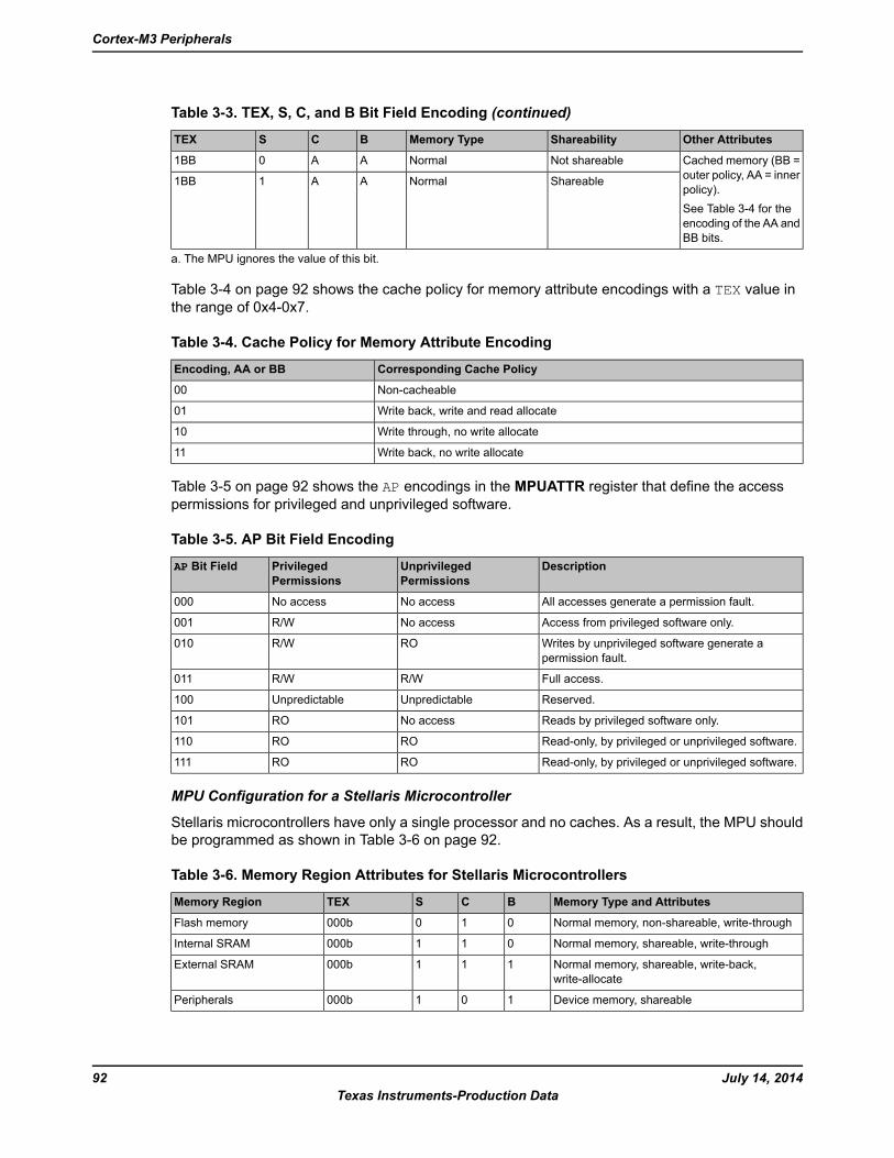
Table 3-3. TEX, S, C, and B Bit Field Encoding (continued)
Other AttributesShareabilityMemory TypeBCSTEX
Cached memory (BB =outer policy, AA = innerpolicy).See Table 3-4 for theencoding of the AA andBB bits.
Not shareableNormalAA01BB
ShareableNormalAA11BB
a. The MPU ignores the value of this bit.
Table 3-4 on page 92 shows the cache policy for memory attribute encodings with a TEX value inthe range of 0x4-0x7.
Table 3-4. Cache Policy for Memory Attribute Encoding
Corresponding Cache PolicyEncoding, AA or BB
Non-cacheable00
Write back, write and read allocate01
Write through, no write allocate10
Write back, no write allocate11
Table 3-5 on page 92 shows the AP encodings in the MPUATTR register that define the accesspermissions for privileged and unprivileged software.
Table 3-5. AP Bit Field Encoding
DescriptionUnprivilegedPermissions
PrivilegedPermissions
AP Bit Field
All accesses generate a permission fault.No accessNo access000
Access from privileged software only.No accessR/W001
Writes by unprivileged software generate apermission fault.
ROR/W010
Full access.R/WR/W011
Reserved.UnpredictableUnpredictable100
Reads by privileged software only.No accessRO101
Read-only, by privileged or unprivileged software.RORO110
Read-only, by privileged or unprivileged software.RORO111
MPU Configuration for a Stellaris Microcontroller
Stellaris microcontrollers have only a single processor and no caches. As a result, the MPU shouldbe programmed as shown in Table 3-6 on page 92.
Table 3-6. Memory Region Attributes for Stellaris Microcontrollers
Memory Type and AttributesBCSTEXMemory Region
Normal memory, non-shareable, write-through010000bFlash memory
Normal memory, shareable, write-through011000bInternal SRAM
Normal memory, shareable, write-back,write-allocate
111000bExternal SRAM
Device memory, shareable101000bPeripherals
July 14, 201492Texas Instruments-Production Data
Cortex-M3 Peripherals
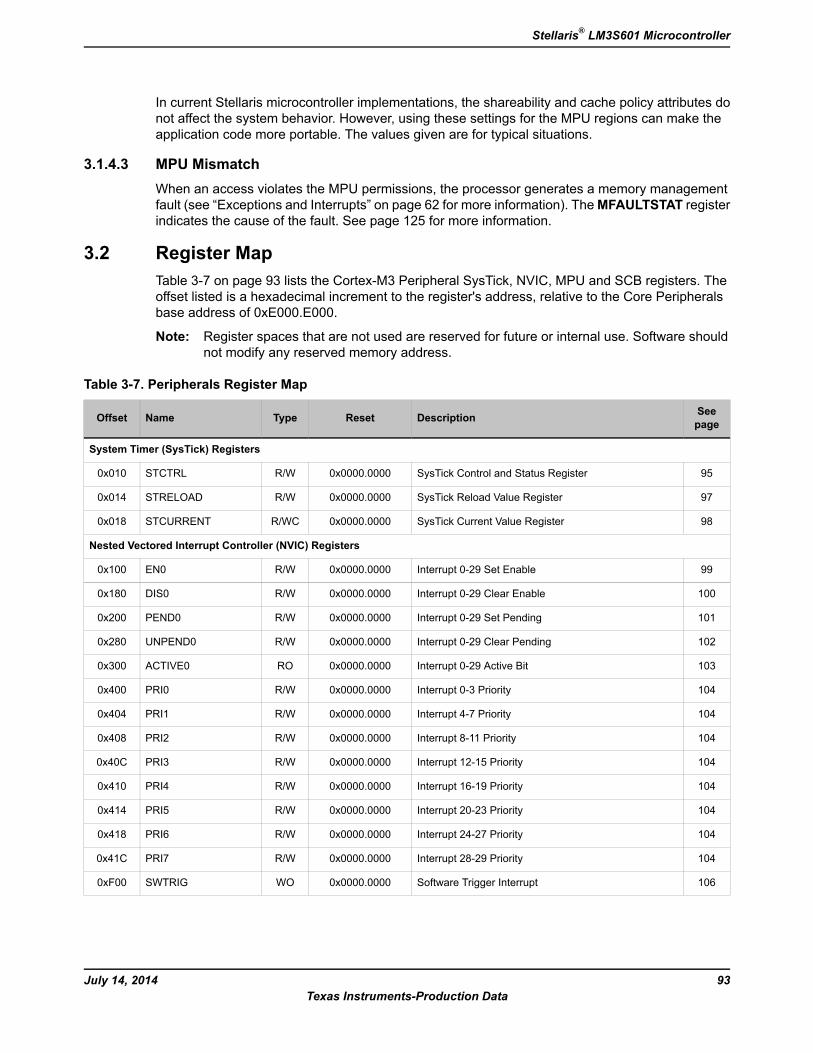
In current Stellaris microcontroller implementations, the shareability and cache policy attributes donot affect the system behavior. However, using these settings for the MPU regions can make theapplication code more portable. The values given are for typical situations.
3.1.4.3 MPU MismatchWhen an access violates the MPU permissions, the processor generates a memory managementfault (see “Exceptions and Interrupts” on page 62 for more information). TheMFAULTSTAT registerindicates the cause of the fault. See page 125 for more information.
3.2 Register MapTable 3-7 on page 93 lists the Cortex-M3 Peripheral SysTick, NVIC, MPU and SCB registers. Theoffset listed is a hexadecimal increment to the register's address, relative to the Core Peripheralsbase address of 0xE000.E000.
Note: Register spaces that are not used are reserved for future or internal use. Software shouldnot modify any reserved memory address.
Table 3-7. Peripherals Register Map
SeepageDescriptionResetTypeNameOffset
System Timer (SysTick) Registers
95SysTick Control and Status Register0x0000.0000R/WSTCTRL0x010
97SysTick Reload Value Register0x0000.0000R/WSTRELOAD0x014
98SysTick Current Value Register0x0000.0000R/WCSTCURRENT0x018
Nested Vectored Interrupt Controller (NVIC) Registers
99Interrupt 0-29 Set Enable0x0000.0000R/WEN00x100
100Interrupt 0-29 Clear Enable0x0000.0000R/WDIS00x180
101Interrupt 0-29 Set Pending0x0000.0000R/WPEND00x200
102Interrupt 0-29 Clear Pending0x0000.0000R/WUNPEND00x280
103Interrupt 0-29 Active Bit0x0000.0000ROACTIVE00x300
104Interrupt 0-3 Priority0x0000.0000R/WPRI00x400
104Interrupt 4-7 Priority0x0000.0000R/WPRI10x404
104Interrupt 8-11 Priority0x0000.0000R/WPRI20x408
104Interrupt 12-15 Priority0x0000.0000R/WPRI30x40C
104Interrupt 16-19 Priority0x0000.0000R/WPRI40x410
104Interrupt 20-23 Priority0x0000.0000R/WPRI50x414
104Interrupt 24-27 Priority0x0000.0000R/WPRI60x418
104Interrupt 28-29 Priority0x0000.0000R/WPRI70x41C
106Software Trigger Interrupt0x0000.0000WOSWTRIG0xF00
93July 14, 2014Texas Instruments-Production Data
Stellaris® LM3S601 Microcontroller
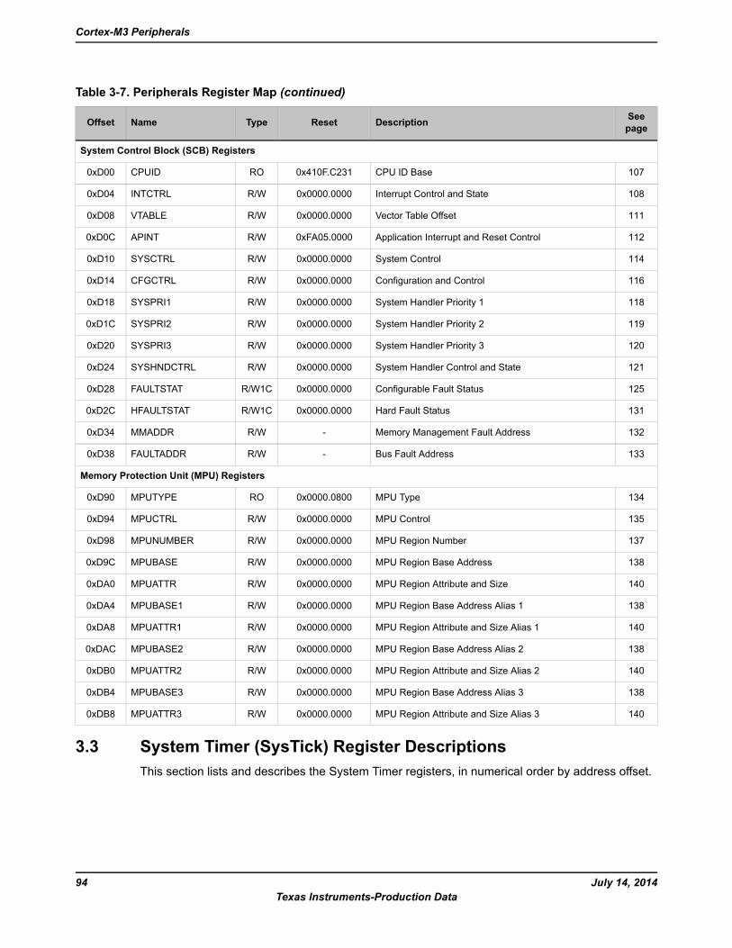
Table 3-7. Peripherals Register Map (continued)
SeepageDescriptionResetTypeNameOffset
System Control Block (SCB) Registers
107CPU ID Base0x410F.C231ROCPUID0xD00
108Interrupt Control and State0x0000.0000R/WINTCTRL0xD04
111Vector Table Offset0x0000.0000R/WVTABLE0xD08
112Application Interrupt and Reset Control0xFA05.0000R/WAPINT0xD0C
114System Control0x0000.0000R/WSYSCTRL0xD10
116Configuration and Control0x0000.0000R/WCFGCTRL0xD14
118System Handler Priority 10x0000.0000R/WSYSPRI10xD18
119System Handler Priority 20x0000.0000R/WSYSPRI20xD1C
120System Handler Priority 30x0000.0000R/WSYSPRI30xD20
121System Handler Control and State0x0000.0000R/WSYSHNDCTRL0xD24
125Configurable Fault Status0x0000.0000R/W1CFAULTSTAT0xD28
131Hard Fault Status0x0000.0000R/W1CHFAULTSTAT0xD2C
132Memory Management Fault Address-R/WMMADDR0xD34
133Bus Fault Address-R/WFAULTADDR0xD38
Memory Protection Unit (MPU) Registers
134MPU Type0x0000.0800ROMPUTYPE0xD90
135MPU Control0x0000.0000R/WMPUCTRL0xD94
137MPU Region Number0x0000.0000R/WMPUNUMBER0xD98
138MPU Region Base Address0x0000.0000R/WMPUBASE0xD9C
140MPU Region Attribute and Size0x0000.0000R/WMPUATTR0xDA0
138MPU Region Base Address Alias 10x0000.0000R/WMPUBASE10xDA4
140MPU Region Attribute and Size Alias 10x0000.0000R/WMPUATTR10xDA8
138MPU Region Base Address Alias 20x0000.0000R/WMPUBASE20xDAC
140MPU Region Attribute and Size Alias 20x0000.0000R/WMPUATTR20xDB0
138MPU Region Base Address Alias 30x0000.0000R/WMPUBASE30xDB4
140MPU Region Attribute and Size Alias 30x0000.0000R/WMPUATTR30xDB8
3.3 System Timer (SysTick) Register DescriptionsThis section lists and describes the System Timer registers, in numerical order by address offset.
July 14, 201494Texas Instruments-Production Data
Cortex-M3 Peripherals
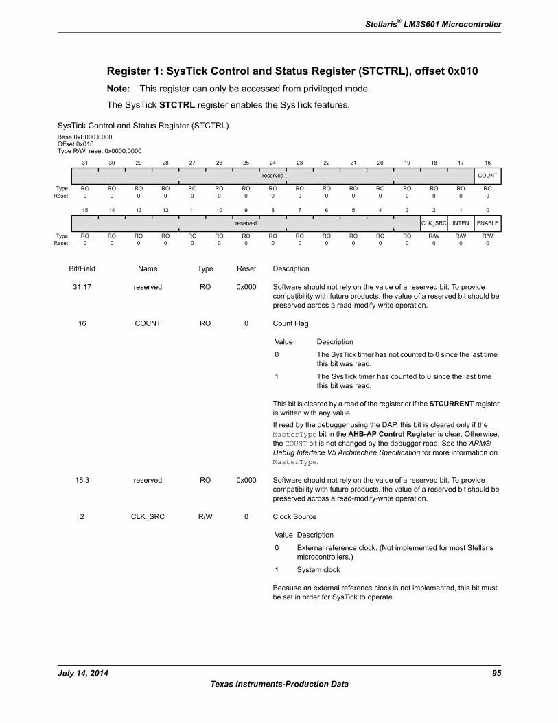
Register 1: SysTick Control and Status Register (STCTRL), offset 0x010Note: This register can only be accessed from privileged mode.
The SysTick STCTRL register enables the SysTick features.
SysTick Control and Status Register (STCTRL)Base 0xE000.E000Offset 0x010Type R/W, reset 0x0000.0000
16171819202122232425262728293031
COUNTreserved
ROROROROROROROROROROROROROROROROType0000000000000000Reset
0123456789101112131415
ENABLEINTENCLK_SRCreserved
R/WR/WR/WROROROROROROROROROROROROROType0000000000000000Reset
DescriptionResetTypeNameBit/Field
Software should not rely on the value of a reserved bit. To providecompatibility with future products, the value of a reserved bit should bepreserved across a read-modify-write operation.
0x000ROreserved31:17
Count Flag
DescriptionValue
The SysTick timer has not counted to 0 since the last timethis bit was read.
0
The SysTick timer has counted to 0 since the last timethis bit was read.
1
This bit is cleared by a read of the register or if the STCURRENT registeris written with any value.If read by the debugger using the DAP, this bit is cleared only if theMasterType bit in the AHB-AP Control Register is clear. Otherwise,the COUNT bit is not changed by the debugger read. See the ARM®Debug Interface V5 Architecture Specification for more information onMasterType.
0ROCOUNT16
Software should not rely on the value of a reserved bit. To providecompatibility with future products, the value of a reserved bit should bepreserved across a read-modify-write operation.
0x000ROreserved15:3
Clock Source
DescriptionValue
External reference clock. (Not implemented for most Stellarismicrocontrollers.)
0
System clock1
Because an external reference clock is not implemented, this bit mustbe set in order for SysTick to operate.
0R/WCLK_SRC2
95July 14, 2014Texas Instruments-Production Data
Stellaris® LM3S601 Microcontroller
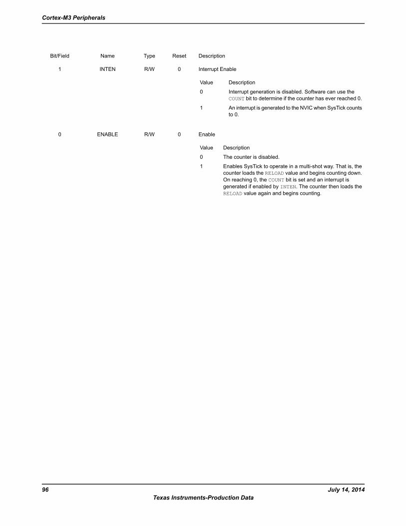
DescriptionResetTypeNameBit/Field
Interrupt Enable
DescriptionValue
Interrupt generation is disabled. Software can use theCOUNT bit to determine if the counter has ever reached 0.
0
An interrupt is generated to the NVIC when SysTick countsto 0.
1
0R/WINTEN1
Enable
DescriptionValue
The counter is disabled.0
Enables SysTick to operate in a multi-shot way. That is, thecounter loads the RELOAD value and begins counting down.On reaching 0, the COUNT bit is set and an interrupt isgenerated if enabled by INTEN. The counter then loads theRELOAD value again and begins counting.
1
0R/WENABLE0
July 14, 201496Texas Instruments-Production Data
Cortex-M3 Peripherals
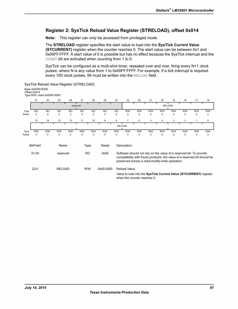
Register 2: SysTick Reload Value Register (STRELOAD), offset 0x014Note: This register can only be accessed from privileged mode.
The STRELOAD register specifies the start value to load into the SysTick Current Value(STCURRENT) register when the counter reaches 0. The start value can be between 0x1 and0x00FF.FFFF. A start value of 0 is possible but has no effect because the SysTick interrupt and theCOUNT bit are activated when counting from 1 to 0.
SysTick can be configured as a multi-shot timer, repeated over and over, firing every N+1 clockpulses, where N is any value from 1 to 0x00FF.FFFF. For example, if a tick interrupt is requiredevery 100 clock pulses, 99 must be written into the RELOAD field.
SysTick Reload Value Register (STRELOAD)Base 0xE000.E000Offset 0x014Type R/W, reset 0x0000.0000
16171819202122232425262728293031
RELOADreserved
R/WR/WR/WR/WR/WR/WR/WR/WROROROROROROROROType0000000000000000Reset
0123456789101112131415
RELOAD
R/WR/WR/WR/WR/WR/WR/WR/WR/WR/WR/WR/WR/WR/WR/WR/WType0000000000000000Reset
DescriptionResetTypeNameBit/Field
Software should not rely on the value of a reserved bit. To providecompatibility with future products, the value of a reserved bit should bepreserved across a read-modify-write operation.
0x00ROreserved31:24
Reload ValueValue to load into the SysTick Current Value (STCURRENT) registerwhen the counter reaches 0.
0x00.0000R/WRELOAD23:0
97July 14, 2014Texas Instruments-Production Data
Stellaris® LM3S601 Microcontroller
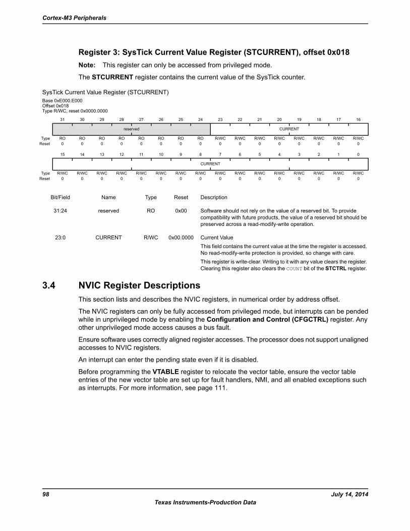
Register 3: SysTick Current Value Register (STCURRENT), offset 0x018Note: This register can only be accessed from privileged mode.
The STCURRENT register contains the current value of the SysTick counter.
SysTick Current Value Register (STCURRENT)Base 0xE000.E000Offset 0x018Type R/WC, reset 0x0000.0000
16171819202122232425262728293031
CURRENTreserved
R/WCR/WCR/WCR/WCR/WCR/WCR/WCR/WCROROROROROROROROType0000000000000000Reset
0123456789101112131415
CURRENT
R/WCR/WCR/WCR/WCR/WCR/WCR/WCR/WCR/WCR/WCR/WCR/WCR/WCR/WCR/WCR/WCType0000000000000000Reset
DescriptionResetTypeNameBit/Field
Software should not rely on the value of a reserved bit. To providecompatibility with future products, the value of a reserved bit should bepreserved across a read-modify-write operation.
0x00ROreserved31:24
Current ValueThis field contains the current value at the time the register is accessed.No read-modify-write protection is provided, so change with care.This register is write-clear. Writing to it with any value clears the register.Clearing this register also clears the COUNT bit of the STCTRL register.
0x00.0000R/WCCURRENT23:0
3.4 NVIC Register DescriptionsThis section lists and describes the NVIC registers, in numerical order by address offset.
The NVIC registers can only be fully accessed from privileged mode, but interrupts can be pendedwhile in unprivileged mode by enabling the Configuration and Control (CFGCTRL) register. Anyother unprivileged mode access causes a bus fault.
Ensure software uses correctly aligned register accesses. The processor does not support unalignedaccesses to NVIC registers.
An interrupt can enter the pending state even if it is disabled.
Before programming the VTABLE register to relocate the vector table, ensure the vector tableentries of the new vector table are set up for fault handlers, NMI, and all enabled exceptions suchas interrupts. For more information, see page 111.
July 14, 201498Texas Instruments-Production Data
Cortex-M3 Peripherals
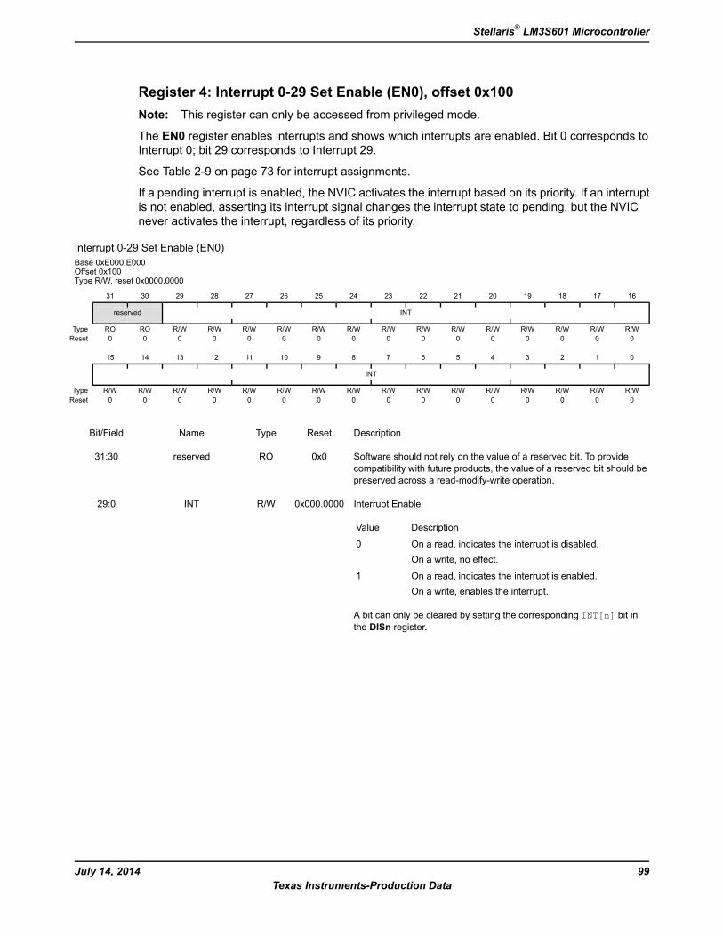
Register 4: Interrupt 0-29 Set Enable (EN0), offset 0x100Note: This register can only be accessed from privileged mode.
The EN0 register enables interrupts and shows which interrupts are enabled. Bit 0 corresponds toInterrupt 0; bit 29 corresponds to Interrupt 29.
See Table 2-9 on page 73 for interrupt assignments.
If a pending interrupt is enabled, the NVIC activates the interrupt based on its priority. If an interruptis not enabled, asserting its interrupt signal changes the interrupt state to pending, but the NVICnever activates the interrupt, regardless of its priority.
Interrupt 0-29 Set Enable (EN0)Base 0xE000.E000Offset 0x100Type R/W, reset 0x0000.0000
16171819202122232425262728293031
INTreserved
R/WR/WR/WR/WR/WR/WR/WR/WR/WR/WR/WR/WR/WR/WROROType0000000000000000Reset
0123456789101112131415
INT
R/WR/WR/WR/WR/WR/WR/WR/WR/WR/WR/WR/WR/WR/WR/WR/WType0000000000000000Reset
DescriptionResetTypeNameBit/Field
Software should not rely on the value of a reserved bit. To providecompatibility with future products, the value of a reserved bit should bepreserved across a read-modify-write operation.
0x0ROreserved31:30
Interrupt Enable
DescriptionValue
On a read, indicates the interrupt is disabled.On a write, no effect.
0
On a read, indicates the interrupt is enabled.On a write, enables the interrupt.
1
A bit can only be cleared by setting the corresponding INT[n] bit inthe DISn register.
0x000.0000R/WINT29:0
99July 14, 2014Texas Instruments-Production Data
Stellaris® LM3S601 Microcontroller
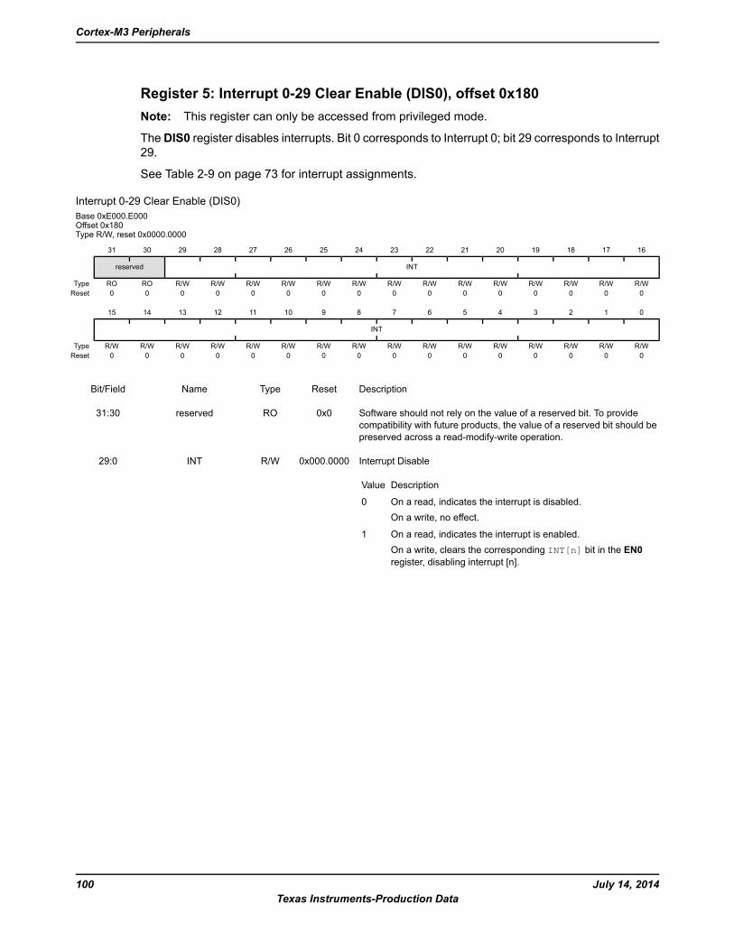
Register 5: Interrupt 0-29 Clear Enable (DIS0), offset 0x180Note: This register can only be accessed from privileged mode.
TheDIS0 register disables interrupts. Bit 0 corresponds to Interrupt 0; bit 29 corresponds to Interrupt29.
See Table 2-9 on page 73 for interrupt assignments.
Interrupt 0-29 Clear Enable (DIS0)Base 0xE000.E000Offset 0x180Type R/W, reset 0x0000.0000
16171819202122232425262728293031
INTreserved
R/WR/WR/WR/WR/WR/WR/WR/WR/WR/WR/WR/WR/WR/WROROType0000000000000000Reset
0123456789101112131415
INT
R/WR/WR/WR/WR/WR/WR/WR/WR/WR/WR/WR/WR/WR/WR/WR/WType0000000000000000Reset
DescriptionResetTypeNameBit/Field
Software should not rely on the value of a reserved bit. To providecompatibility with future products, the value of a reserved bit should bepreserved across a read-modify-write operation.
0x0ROreserved31:30
Interrupt Disable
DescriptionValue
On a read, indicates the interrupt is disabled.On a write, no effect.
0
On a read, indicates the interrupt is enabled.On a write, clears the corresponding INT[n] bit in the EN0register, disabling interrupt [n].
1
0x000.0000R/WINT29:0
July 14, 2014100Texas Instruments-Production Data
Cortex-M3 Peripherals
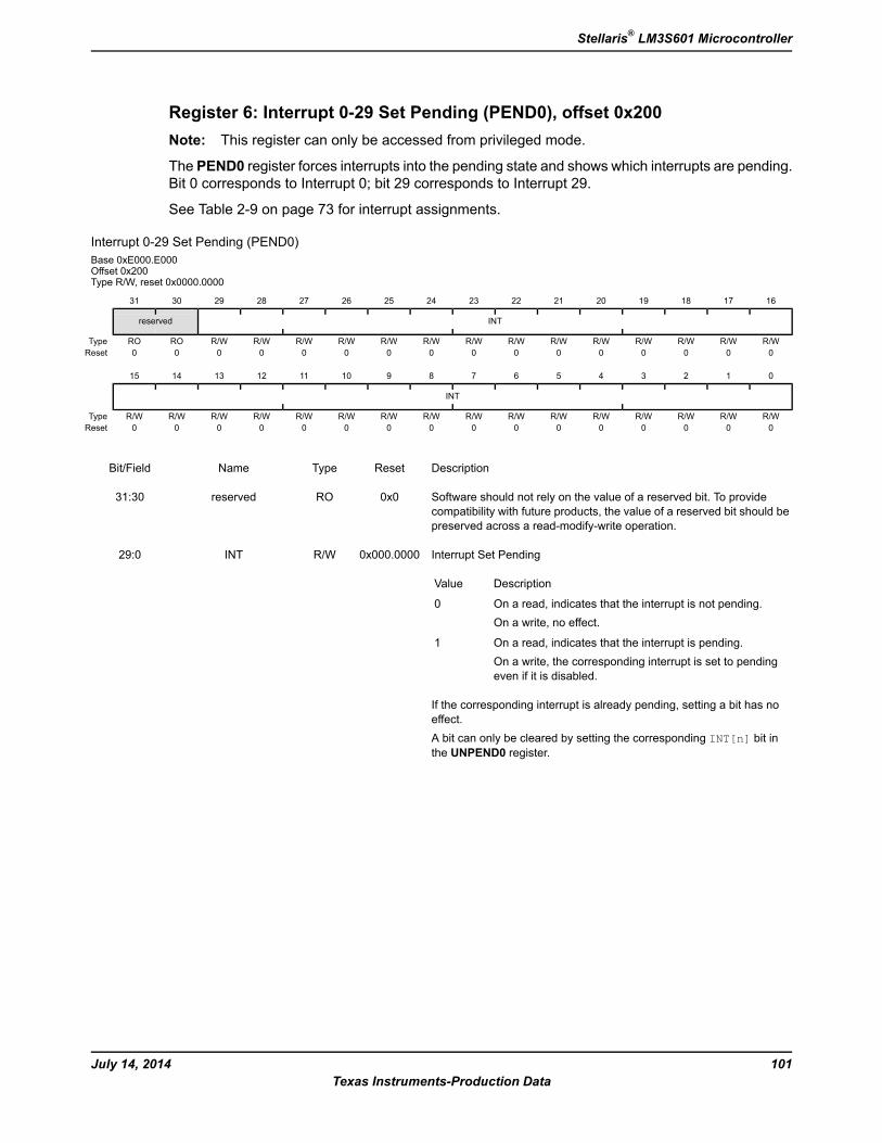
Register 6: Interrupt 0-29 Set Pending (PEND0), offset 0x200Note: This register can only be accessed from privileged mode.
The PEND0 register forces interrupts into the pending state and shows which interrupts are pending.Bit 0 corresponds to Interrupt 0; bit 29 corresponds to Interrupt 29.
See Table 2-9 on page 73 for interrupt assignments.
Interrupt 0-29 Set Pending (PEND0)Base 0xE000.E000Offset 0x200Type R/W, reset 0x0000.0000
16171819202122232425262728293031
INTreserved
R/WR/WR/WR/WR/WR/WR/WR/WR/WR/WR/WR/WR/WR/WROROType0000000000000000Reset
0123456789101112131415
INT
R/WR/WR/WR/WR/WR/WR/WR/WR/WR/WR/WR/WR/WR/WR/WR/WType0000000000000000Reset
DescriptionResetTypeNameBit/Field
Software should not rely on the value of a reserved bit. To providecompatibility with future products, the value of a reserved bit should bepreserved across a read-modify-write operation.
0x0ROreserved31:30
Interrupt Set Pending
DescriptionValue
On a read, indicates that the interrupt is not pending.On a write, no effect.
0
On a read, indicates that the interrupt is pending.On a write, the corresponding interrupt is set to pendingeven if it is disabled.
1
If the corresponding interrupt is already pending, setting a bit has noeffect.A bit can only be cleared by setting the corresponding INT[n] bit inthe UNPEND0 register.
0x000.0000R/WINT29:0
101July 14, 2014Texas Instruments-Production Data
Stellaris® LM3S601 Microcontroller
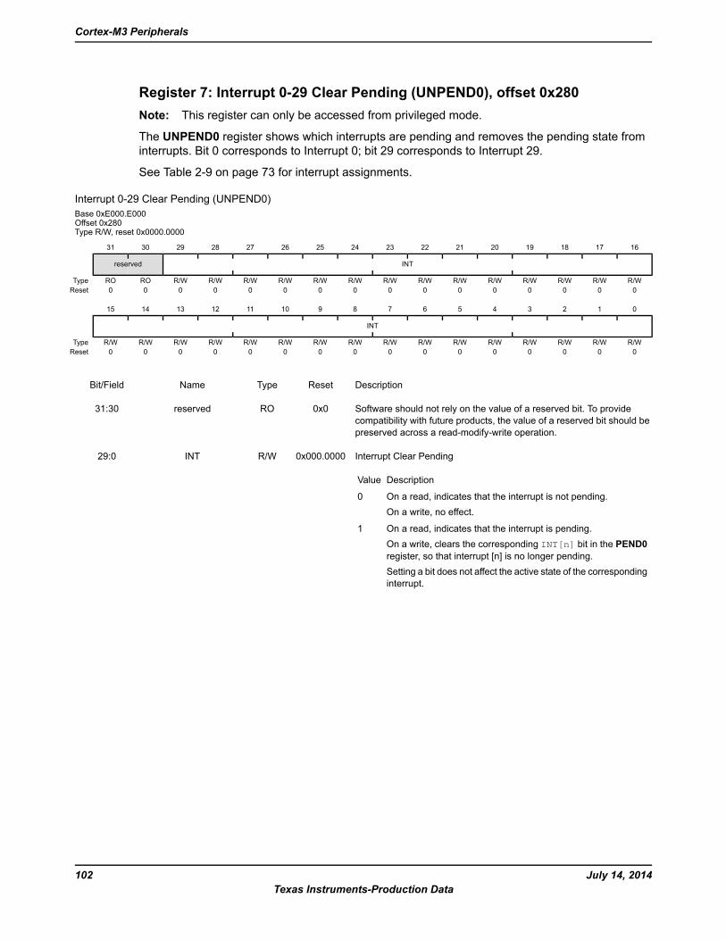
Register 7: Interrupt 0-29 Clear Pending (UNPEND0), offset 0x280Note: This register can only be accessed from privileged mode.
The UNPEND0 register shows which interrupts are pending and removes the pending state frominterrupts. Bit 0 corresponds to Interrupt 0; bit 29 corresponds to Interrupt 29.
See Table 2-9 on page 73 for interrupt assignments.
Interrupt 0-29 Clear Pending (UNPEND0)Base 0xE000.E000Offset 0x280Type R/W, reset 0x0000.0000
16171819202122232425262728293031
INTreserved
R/WR/WR/WR/WR/WR/WR/WR/WR/WR/WR/WR/WR/WR/WROROType0000000000000000Reset
0123456789101112131415
INT
R/WR/WR/WR/WR/WR/WR/WR/WR/WR/WR/WR/WR/WR/WR/WR/WType0000000000000000Reset
DescriptionResetTypeNameBit/Field
Software should not rely on the value of a reserved bit. To providecompatibility with future products, the value of a reserved bit should bepreserved across a read-modify-write operation.
0x0ROreserved31:30
Interrupt Clear Pending
DescriptionValue
On a read, indicates that the interrupt is not pending.On a write, no effect.
0
On a read, indicates that the interrupt is pending.On a write, clears the corresponding INT[n] bit in the PEND0register, so that interrupt [n] is no longer pending.Setting a bit does not affect the active state of the correspondinginterrupt.
1
0x000.0000R/WINT29:0
July 14, 2014102Texas Instruments-Production Data
Cortex-M3 Peripherals
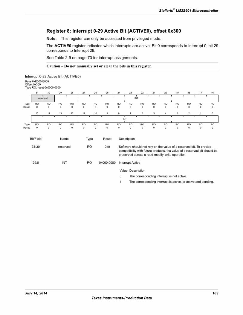
Register 8: Interrupt 0-29 Active Bit (ACTIVE0), offset 0x300Note: This register can only be accessed from privileged mode.
The ACTIVE0 register indicates which interrupts are active. Bit 0 corresponds to Interrupt 0; bit 29corresponds to Interrupt 29.
See Table 2-9 on page 73 for interrupt assignments.
Caution – Do not manually set or clear the bits in this register.
Interrupt 0-29 Active Bit (ACTIVE0)Base 0xE000.E000Offset 0x300Type RO, reset 0x0000.0000
16171819202122232425262728293031
INTreserved
ROROROROROROROROROROROROROROROROType0000000000000000Reset
0123456789101112131415
INT
ROROROROROROROROROROROROROROROROType0000000000000000Reset
DescriptionResetTypeNameBit/Field
Software should not rely on the value of a reserved bit. To providecompatibility with future products, the value of a reserved bit should bepreserved across a read-modify-write operation.
0x0ROreserved31:30
Interrupt Active
DescriptionValue
The corresponding interrupt is not active.0
The corresponding interrupt is active, or active and pending.1
0x000.0000ROINT29:0
103July 14, 2014Texas Instruments-Production Data
Stellaris® LM3S601 Microcontroller
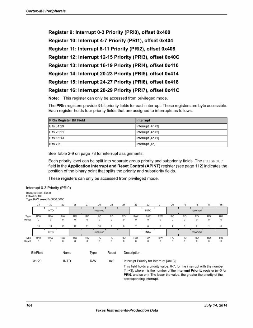
Register 9: Interrupt 0-3 Priority (PRI0), offset 0x400Register 10: Interrupt 4-7 Priority (PRI1), offset 0x404Register 11: Interrupt 8-11 Priority (PRI2), offset 0x408Register 12: Interrupt 12-15 Priority (PRI3), offset 0x40CRegister 13: Interrupt 16-19 Priority (PRI4), offset 0x410Register 14: Interrupt 20-23 Priority (PRI5), offset 0x414Register 15: Interrupt 24-27 Priority (PRI6), offset 0x418Register 16: Interrupt 28-29 Priority (PRI7), offset 0x41CNote: This register can only be accessed from privileged mode.
The PRIn registers provide 3-bit priority fields for each interrupt. These registers are byte accessible.Each register holds four priority fields that are assigned to interrupts as follows:
InterruptPRIn Register Bit Field
Interrupt [4n+3]Bits 31:29
Interrupt [4n+2]Bits 23:21
Interrupt [4n+1]Bits 15:13
Interrupt [4n]Bits 7:5
See Table 2-9 on page 73 for interrupt assignments.
Each priority level can be split into separate group priority and subpriority fields. The PRIGROUPfield in the Application Interrupt and Reset Control (APINT) register (see page 112) indicates theposition of the binary point that splits the priority and subpriority fields.
These registers can only be accessed from privileged mode.
Interrupt 0-3 Priority (PRI0)Base 0xE000.E000Offset 0x400Type R/W, reset 0x0000.0000
16171819202122232425262728293031
reservedINTCreservedINTD
ROROROROROR/WR/WR/WROROROROROR/WR/WR/WType0000000000000000Reset
0123456789101112131415
reservedINTAreservedINTB
ROROROROROR/WR/WR/WROROROROROR/WR/WR/WType0000000000000000Reset
DescriptionResetTypeNameBit/Field
Interrupt Priority for Interrupt [4n+3]This field holds a priority value, 0-7, for the interrupt with the number[4n+3], where n is the number of the Interrupt Priority register (n=0 forPRI0, and so on). The lower the value, the greater the priority of thecorresponding interrupt.
0x0R/WINTD31:29
July 14, 2014104Texas Instruments-Production Data
Cortex-M3 Peripherals
DescriptionResetTypeNameBit/Field
Software should not rely on the value of a reserved bit. To providecompatibility with future products, the value of a reserved bit should bepreserved across a read-modify-write operation.
0x0ROreserved28:24
Interrupt Priority for Interrupt [4n+2]This field holds a priority value, 0-7, for the interrupt with the number[4n+2], where n is the number of the Interrupt Priority register (n=0 forPRI0, and so on). The lower the value, the greater the priority of thecorresponding interrupt.
0x0R/WINTC23:21
Software should not rely on the value of a reserved bit. To providecompatibility with future products, the value of a reserved bit should bepreserved across a read-modify-write operation.
0x0ROreserved20:16
Interrupt Priority for Interrupt [4n+1]This field holds a priority value, 0-7, for the interrupt with the number[4n+1], where n is the number of the Interrupt Priority register (n=0 forPRI0, and so on). The lower the value, the greater the priority of thecorresponding interrupt.
0x0R/WINTB15:13
Software should not rely on the value of a reserved bit. To providecompatibility with future products, the value of a reserved bit should bepreserved across a read-modify-write operation.
0x0ROreserved12:8
Interrupt Priority for Interrupt [4n]This field holds a priority value, 0-7, for the interrupt with the number[4n], where n is the number of the Interrupt Priority register (n=0 forPRI0, and so on). The lower the value, the greater the priority of thecorresponding interrupt.
0x0R/WINTA7:5
Software should not rely on the value of a reserved bit. To providecompatibility with future products, the value of a reserved bit should bepreserved across a read-modify-write operation.
0x0ROreserved4:0
105July 14, 2014Texas Instruments-Production Data
Stellaris® LM3S601 Microcontroller
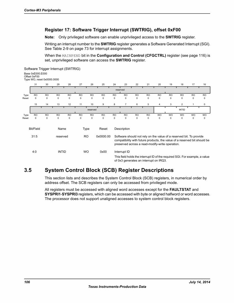
Register 17: Software Trigger Interrupt (SWTRIG), offset 0xF00Note: Only privileged software can enable unprivileged access to the SWTRIG register.
Writing an interrupt number to the SWTRIG register generates a Software Generated Interrupt (SGI).See Table 2-9 on page 73 for interrupt assignments.
When the MAINPEND bit in the Configuration and Control (CFGCTRL) register (see page 116) isset, unprivileged software can access the SWTRIG register.
Software Trigger Interrupt (SWTRIG)Base 0xE000.E000Offset 0xF00Type WO, reset 0x0000.0000
16171819202122232425262728293031
reserved
ROROROROROROROROROROROROROROROROType0000000000000000Reset
0123456789101112131415
INTIDreserved
WOWOWOWOWOROROROROROROROROROROROType0000000000000000Reset
DescriptionResetTypeNameBit/Field
Software should not rely on the value of a reserved bit. To providecompatibility with future products, the value of a reserved bit should bepreserved across a read-modify-write operation.
0x0000.00ROreserved31:5
Interrupt IDThis field holds the interrupt ID of the required SGI. For example, a valueof 0x3 generates an interrupt on IRQ3.
0x00WOINTID4:0
3.5 System Control Block (SCB) Register DescriptionsThis section lists and describes the System Control Block (SCB) registers, in numerical order byaddress offset. The SCB registers can only be accessed from privileged mode.
All registers must be accessed with aligned word accesses except for the FAULTSTAT andSYSPRI1-SYSPRI3 registers, which can be accessed with byte or aligned halfword or word accesses.The processor does not support unaligned accesses to system control block registers.
July 14, 2014106Texas Instruments-Production Data
Cortex-M3 Peripherals
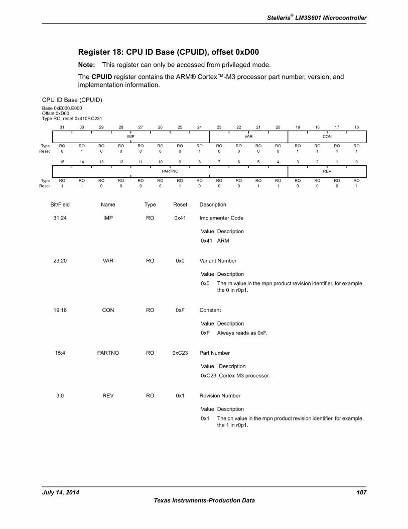
Register 18: CPU ID Base (CPUID), offset 0xD00Note: This register can only be accessed from privileged mode.
The CPUID register contains the ARM® Cortex™-M3 processor part number, version, andimplementation information.
CPU ID Base (CPUID)Base 0xE000.E000Offset 0xD00Type RO, reset 0x410F.C231
16171819202122232425262728293031
CONVARIMP
ROROROROROROROROROROROROROROROROType1111000010000010Reset
0123456789101112131415
REVPARTNO
ROROROROROROROROROROROROROROROROType1000110001000011Reset
DescriptionResetTypeNameBit/Field
Implementer Code
DescriptionValue
ARM0x41
0x41ROIMP31:24
Variant Number
DescriptionValue
The rn value in the rnpn product revision identifier, for example,the 0 in r0p1.
0x0
0x0ROVAR23:20
Constant
DescriptionValue
Always reads as 0xF.0xF
0xFROCON19:16
Part Number
DescriptionValue
Cortex-M3 processor.0xC23
0xC23ROPARTNO15:4
Revision Number
DescriptionValue
The pn value in the rnpn product revision identifier, for example,the 1 in r0p1.
0x1
0x1ROREV3:0
107July 14, 2014Texas Instruments-Production Data
Stellaris® LM3S601 Microcontroller
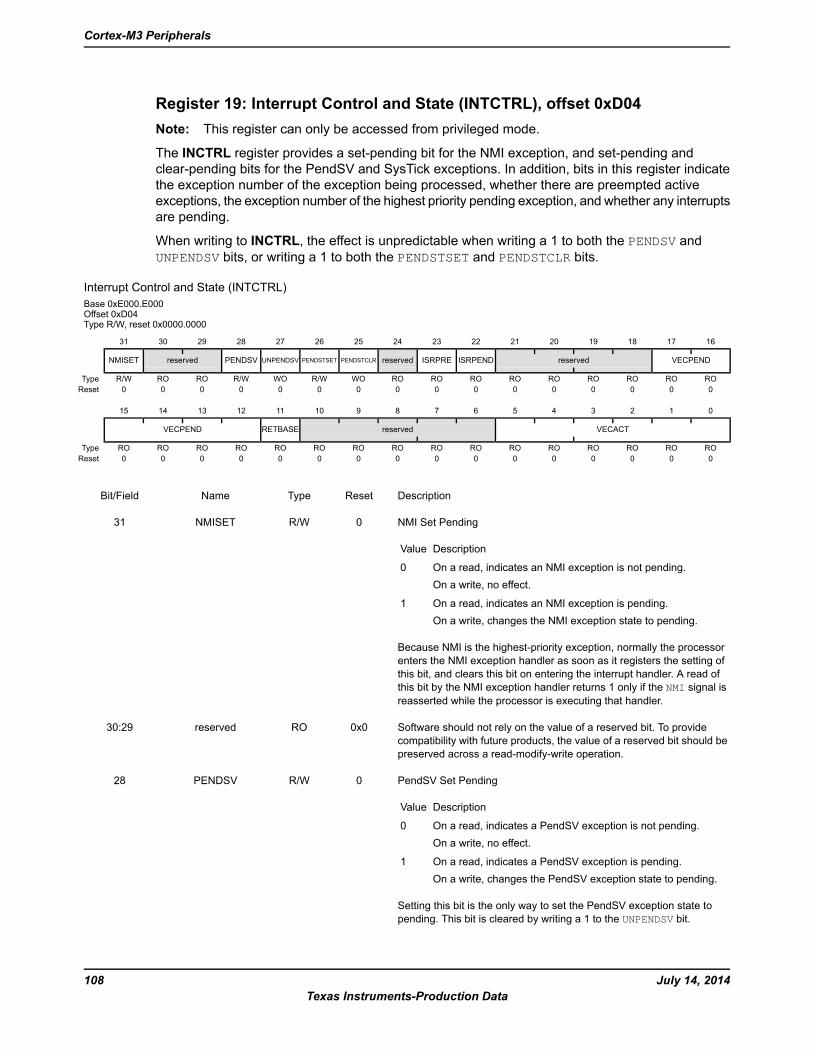
Register 19: Interrupt Control and State (INTCTRL), offset 0xD04Note: This register can only be accessed from privileged mode.
The INCTRL register provides a set-pending bit for the NMI exception, and set-pending andclear-pending bits for the PendSV and SysTick exceptions. In addition, bits in this register indicatethe exception number of the exception being processed, whether there are preempted activeexceptions, the exception number of the highest priority pending exception, and whether any interruptsare pending.
When writing to INCTRL, the effect is unpredictable when writing a 1 to both the PENDSV andUNPENDSV bits, or writing a 1 to both the PENDSTSET and PENDSTCLR bits.
Interrupt Control and State (INTCTRL)Base 0xE000.E000Offset 0xD04Type R/W, reset 0x0000.0000
16171819202122232425262728293031
VECPENDreservedISRPENDISRPREreservedPENDSTCLRPENDSTSETUNPENDSVPENDSVreservedNMISET
ROROROROROROROROROWOR/WWOR/WROROR/WType0000000000000000Reset
0123456789101112131415
VECACTreservedRETBASEVECPEND
ROROROROROROROROROROROROROROROROType0000000000000000Reset
DescriptionResetTypeNameBit/Field
NMI Set Pending
DescriptionValue
On a read, indicates an NMI exception is not pending.On a write, no effect.
0
On a read, indicates an NMI exception is pending.On a write, changes the NMI exception state to pending.
1
Because NMI is the highest-priority exception, normally the processorenters the NMI exception handler as soon as it registers the setting ofthis bit, and clears this bit on entering the interrupt handler. A read ofthis bit by the NMI exception handler returns 1 only if the NMI signal isreasserted while the processor is executing that handler.
0R/WNMISET31
Software should not rely on the value of a reserved bit. To providecompatibility with future products, the value of a reserved bit should bepreserved across a read-modify-write operation.
0x0ROreserved30:29
PendSV Set Pending
DescriptionValue
On a read, indicates a PendSV exception is not pending.On a write, no effect.
0
On a read, indicates a PendSV exception is pending.On a write, changes the PendSV exception state to pending.
1
Setting this bit is the only way to set the PendSV exception state topending. This bit is cleared by writing a 1 to the UNPENDSV bit.
0R/WPENDSV28
July 14, 2014108Texas Instruments-Production Data
Cortex-M3 Peripherals
DescriptionResetTypeNameBit/Field
PendSV Clear Pending
DescriptionValue
On a write, no effect.0
On a write, removes the pending state from the PendSVexception.
1
This bit is write only; on a register read, its value is unknown.
0WOUNPENDSV27
SysTick Set Pending
DescriptionValue
On a read, indicates a SysTick exception is not pending.On a write, no effect.
0
On a read, indicates a SysTick exception is pending.On a write, changes the SysTick exception state to pending.
1
This bit is cleared by writing a 1 to the PENDSTCLR bit.
0R/WPENDSTSET26
SysTick Clear Pending
DescriptionValue
On a write, no effect.0
On a write, removes the pending state from the SysTickexception.
1
This bit is write only; on a register read, its value is unknown.
0WOPENDSTCLR25
Software should not rely on the value of a reserved bit. To providecompatibility with future products, the value of a reserved bit should bepreserved across a read-modify-write operation.
0ROreserved24
Debug Interrupt Handling
DescriptionValue
The release from halt does not take an interrupt.0
The release from halt takes an interrupt.1
This bit is only meaningful in Debug mode and reads as zero when theprocessor is not in Debug mode.
0ROISRPRE23
Interrupt Pending
DescriptionValue
No interrupt is pending.0
An interrupt is pending.1
This bit provides status for all interrupts excluding NMI and Faults.
0ROISRPEND22
Software should not rely on the value of a reserved bit. To providecompatibility with future products, the value of a reserved bit should bepreserved across a read-modify-write operation.
0x0ROreserved21:18
109July 14, 2014Texas Instruments-Production Data
Stellaris® LM3S601 Microcontroller
DescriptionResetTypeNameBit/Field
Interrupt Pending Vector NumberThis field contains the exception number of the highest priority pendingenabled exception. The value indicated by this field includes the effectof the BASEPRI and FAULTMASK registers, but not any effect of thePRIMASK register.
DescriptionValue
No exceptions are pending0x00
Reserved0x01
NMI0x02
Hard fault0x03
Memory management fault0x04
Bus fault0x05
Usage fault0x06
Reserved0x07-0x0A
SVCall0x0B
Reserved for Debug0x0C
Reserved0x0D
PendSV0x0E
SysTick0x0F
Interrupt Vector 00x10
Interrupt Vector 10x11
......
Interrupt Vector 290x2D
Reserved0x2E-0x3F
0x00ROVECPEND17:12
Return to Base
DescriptionValue
There are preempted active exceptions to execute.0
There are no active exceptions, or the currently executingexception is the only active exception.
1
This bit provides status for all interrupts excluding NMI and Faults. Thisbit only has meaning if the processor is currently executing an ISR (theInterrupt Program Status (IPSR) register is non-zero).
0RORETBASE11
Software should not rely on the value of a reserved bit. To providecompatibility with future products, the value of a reserved bit should bepreserved across a read-modify-write operation.
0x0ROreserved10:6
Interrupt Pending Vector NumberThis field contains the active exception number. The exception numberscan be found in the description for the VECPEND field. If this field is clear,the processor is in Thread mode. This field contains the same value asthe ISRNUM field in the IPSR register.Subtract 16 from this value to obtain the IRQ number required to indexinto the Interrupt Set Enable (ENn), Interrupt Clear Enable (DISn),Interrupt Set Pending (PENDn), Interrupt Clear Pending (UNPENDn),and Interrupt Priority (PRIn) registers (see page 54).
0x00ROVECACT5:0
July 14, 2014110Texas Instruments-Production Data
Cortex-M3 Peripherals
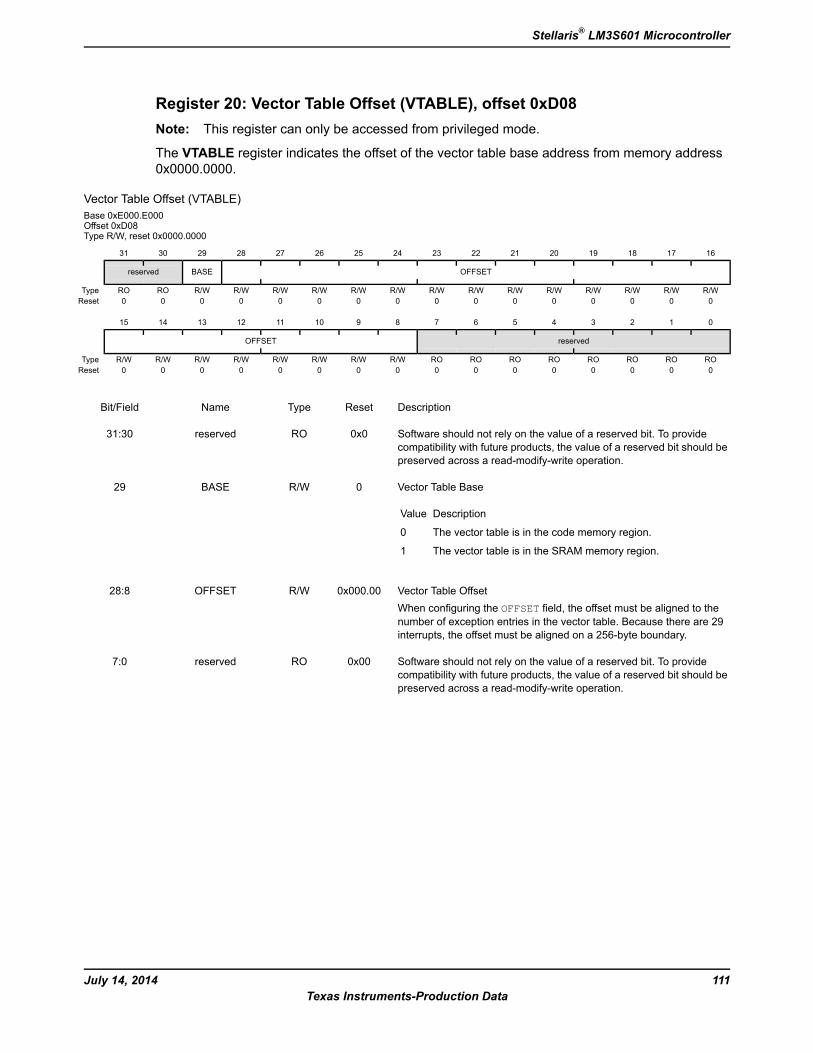
Register 20: Vector Table Offset (VTABLE), offset 0xD08Note: This register can only be accessed from privileged mode.
The VTABLE register indicates the offset of the vector table base address from memory address0x0000.0000.
Vector Table Offset (VTABLE)Base 0xE000.E000Offset 0xD08Type R/W, reset 0x0000.0000
16171819202122232425262728293031
OFFSETBASEreserved
R/WR/WR/WR/WR/WR/WR/WR/WR/WR/WR/WR/WR/WR/WROROType0000000000000000Reset
0123456789101112131415
reservedOFFSET
ROROROROROROROROR/WR/WR/WR/WR/WR/WR/WR/WType0000000000000000Reset
DescriptionResetTypeNameBit/Field
Software should not rely on the value of a reserved bit. To providecompatibility with future products, the value of a reserved bit should bepreserved across a read-modify-write operation.
0x0ROreserved31:30
Vector Table Base
DescriptionValue
The vector table is in the code memory region.0
The vector table is in the SRAM memory region.1
0R/WBASE29
Vector Table OffsetWhen configuring the OFFSET field, the offset must be aligned to thenumber of exception entries in the vector table. Because there are 29interrupts, the offset must be aligned on a 256-byte boundary.
0x000.00R/WOFFSET28:8
Software should not rely on the value of a reserved bit. To providecompatibility with future products, the value of a reserved bit should bepreserved across a read-modify-write operation.
0x00ROreserved7:0
111July 14, 2014Texas Instruments-Production Data
Stellaris® LM3S601 Microcontroller
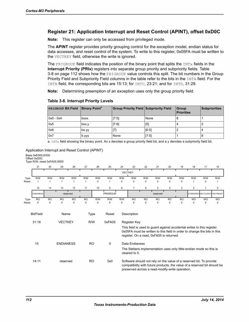
Register 21: Application Interrupt and Reset Control (APINT), offset 0xD0CNote: This register can only be accessed from privileged mode.
The APINT register provides priority grouping control for the exception model, endian status fordata accesses, and reset control of the system. To write to this register, 0x05FA must be written tothe VECTKEY field, otherwise the write is ignored.
The PRIGROUP field indicates the position of the binary point that splits the INTx fields in theInterrupt Priority (PRIx) registers into separate group priority and subpriority fields. Table3-8 on page 112 shows how the PRIGROUP value controls this split. The bit numbers in the GroupPriority Field and Subpriority Field columns in the table refer to the bits in the INTA field. For theINTB field, the corresponding bits are 15:13; for INTC, 23:21; and for INTD, 31:29.
Note: Determining preemption of an exception uses only the group priority field.
Table 3-8. Interrupt Priority Levels
SubprioritiesGroupPriorities
Subpriority FieldGroup Priority FieldBinary PointaPRIGROUP Bit Field
18None[7:5]bxxx.0x0 - 0x4
24[5][7:6]bxx.y0x5
42[6:5][7]bx.yy0x6
81[7:5]Noneb.yyy0x7
a. INTx field showing the binary point. An x denotes a group priority field bit, and a y denotes a subpriority field bit.
Application Interrupt and Reset Control (APINT)Base 0xE000.E000Offset 0xD0CType R/W, reset 0xFA05.0000
16171819202122232425262728293031
VECTKEY
R/WR/WR/WR/WR/WR/WR/WR/WR/WR/WR/WR/WR/WR/WR/WR/WType1010000001011111Reset
0123456789101112131415
VECTRESETVECTCLRACTSYSRESREQreservedPRIGROUPreservedENDIANESS
WOWOWOROROROROROR/WR/WR/WROROROROROType0000000000000000Reset
DescriptionResetTypeNameBit/Field
Register KeyThis field is used to guard against accidental writes to this register.0x05FA must be written to this field in order to change the bits in thisregister. On a read, 0xFA05 is returned.
0xFA05R/WVECTKEY31:16
Data EndianessThe Stellaris implementation uses only little-endian mode so this iscleared to 0.
0ROENDIANESS15
Software should not rely on the value of a reserved bit. To providecompatibility with future products, the value of a reserved bit should bepreserved across a read-modify-write operation.
0x0ROreserved14:11
July 14, 2014112Texas Instruments-Production Data
Cortex-M3 Peripherals
DescriptionResetTypeNameBit/Field
Interrupt Priority GroupingThis field determines the split of group priority from subpriority (seeTable 3-8 on page 112 for more information).
0x0R/WPRIGROUP10:8
Software should not rely on the value of a reserved bit. To providecompatibility with future products, the value of a reserved bit should bepreserved across a read-modify-write operation.
0x0ROreserved7:3
System Reset Request
DescriptionValue
No effect.0
Resets the core and all on-chip peripherals except the Debuginterface.
1
This bit is automatically cleared during the reset of the core and readsas 0.
0WOSYSRESREQ2
Clear Active NMI / FaultThis bit is reserved for Debug use and reads as 0. This bit must bewritten as a 0, otherwise behavior is unpredictable.
0WOVECTCLRACT1
System ResetThis bit is reserved for Debug use and reads as 0. This bit must bewritten as a 0, otherwise behavior is unpredictable.
0WOVECTRESET0
113July 14, 2014Texas Instruments-Production Data
Stellaris® LM3S601 Microcontroller
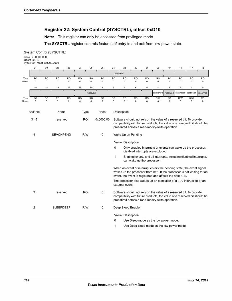
Register 22: System Control (SYSCTRL), offset 0xD10Note: This register can only be accessed from privileged mode.
The SYSCTRL register controls features of entry to and exit from low-power state.
System Control (SYSCTRL)Base 0xE000.E000Offset 0xD10Type R/W, reset 0x0000.0000
16171819202122232425262728293031
reserved
ROROROROROROROROROROROROROROROROType0000000000000000Reset
0123456789101112131415
reservedSLEEPEXITSLEEPDEEPreservedSEVONPENDreserved
ROR/WR/WROR/WROROROROROROROROROROROType0000000000000000Reset
DescriptionResetTypeNameBit/Field
Software should not rely on the value of a reserved bit. To providecompatibility with future products, the value of a reserved bit should bepreserved across a read-modify-write operation.
0x0000.00ROreserved31:5
Wake Up on Pending
DescriptionValue
Only enabled interrupts or events can wake up the processor;disabled interrupts are excluded.
0
Enabled events and all interrupts, including disabled interrupts,can wake up the processor.
1
When an event or interrupt enters the pending state, the event signalwakes up the processor from WFE. If the processor is not waiting for anevent, the event is registered and affects the next WFE.The processor also wakes up on execution of a SEV instruction or anexternal event.
0R/WSEVONPEND4
Software should not rely on the value of a reserved bit. To providecompatibility with future products, the value of a reserved bit should bepreserved across a read-modify-write operation.
0ROreserved3
Deep Sleep Enable
DescriptionValue
Use Sleep mode as the low power mode.0
Use Deep-sleep mode as the low power mode.1
0R/WSLEEPDEEP2
July 14, 2014114Texas Instruments-Production Data
Cortex-M3 Peripherals
DescriptionResetTypeNameBit/Field
Sleep on ISR Exit
DescriptionValue
When returning from Handler mode to Thread mode, do notsleep when returning to Thread mode.
0
When returning fromHandler mode to Threadmode, enter sleepor deep sleep on return from an ISR.
1
Setting this bit enables an interrupt-driven application to avoid returningto an empty main application.
0R/WSLEEPEXIT1
Software should not rely on the value of a reserved bit. To providecompatibility with future products, the value of a reserved bit should bepreserved across a read-modify-write operation.
0ROreserved0
115July 14, 2014Texas Instruments-Production Data
Stellaris® LM3S601 Microcontroller
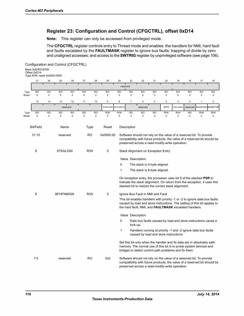
Register 23: Configuration and Control (CFGCTRL), offset 0xD14Note: This register can only be accessed from privileged mode.
The CFGCTRL register controls entry to Thread mode and enables: the handlers for NMI, hard faultand faults escalated by the FAULTMASK register to ignore bus faults; trapping of divide by zeroand unaligned accesses; and access to theSWTRIG register by unprivileged software (see page 106).
Configuration and Control (CFGCTRL)Base 0xE000.E000Offset 0xD14Type R/W, reset 0x0000.0000
16171819202122232425262728293031
reserved
ROROROROROROROROROROROROROROROROType0000000000000000Reset
0123456789101112131415
BASETHRMAINPENDreservedUNALIGNEDDIV0reservedBFHFNMIGNSTKALIGNreserved
R/WR/WROR/WR/WROROROR/WR/WROROROROROROType0000000000000000Reset
DescriptionResetTypeNameBit/Field
Software should not rely on the value of a reserved bit. To providecompatibility with future products, the value of a reserved bit should bepreserved across a read-modify-write operation.
0x0000.00ROreserved31:10
Stack Alignment on Exception Entry
DescriptionValue
The stack is 4-byte aligned.0
The stack is 8-byte aligned.1
On exception entry, the processor uses bit 9 of the stacked PSR toindicate the stack alignment. On return from the exception, it uses thisstacked bit to restore the correct stack alignment.
0R/WSTKALIGN9
Ignore Bus Fault in NMI and FaultThis bit enables handlers with priority -1 or -2 to ignore data bus faultscaused by load and store instructions. The setting of this bit applies tothe hard fault, NMI, and FAULTMASK escalated handlers.
DescriptionValue
Data bus faults caused by load and store instructions cause alock-up.
0
Handlers running at priority -1 and -2 ignore data bus faultscaused by load and store instructions.
1
Set this bit only when the handler and its data are in absolutely safememory. The normal use of this bit is to probe system devices andbridges to detect control path problems and fix them.
0R/WBFHFNMIGN8
Software should not rely on the value of a reserved bit. To providecompatibility with future products, the value of a reserved bit should bepreserved across a read-modify-write operation.
0x0ROreserved7:5
July 14, 2014116Texas Instruments-Production Data
Cortex-M3 Peripherals
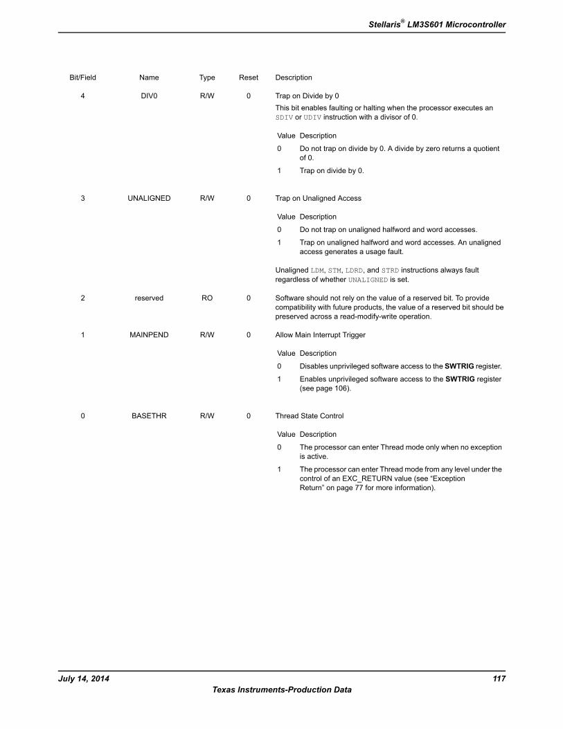
DescriptionResetTypeNameBit/Field
Trap on Divide by 0This bit enables faulting or halting when the processor executes anSDIV or UDIV instruction with a divisor of 0.
DescriptionValue
Do not trap on divide by 0. A divide by zero returns a quotientof 0.
0
Trap on divide by 0.1
0R/WDIV04
Trap on Unaligned Access
DescriptionValue
Do not trap on unaligned halfword and word accesses.0
Trap on unaligned halfword and word accesses. An unalignedaccess generates a usage fault.
1
Unaligned LDM, STM, LDRD, and STRD instructions always faultregardless of whether UNALIGNED is set.
0R/WUNALIGNED3
Software should not rely on the value of a reserved bit. To providecompatibility with future products, the value of a reserved bit should bepreserved across a read-modify-write operation.
0ROreserved2
Allow Main Interrupt Trigger
DescriptionValue
Disables unprivileged software access to the SWTRIG register.0
Enables unprivileged software access to the SWTRIG register(see page 106).
1
0R/WMAINPEND1
Thread State Control
DescriptionValue
The processor can enter Thread mode only when no exceptionis active.
0
The processor can enter Thread mode from any level under thecontrol of an EXC_RETURN value (see “ExceptionReturn” on page 77 for more information).
1
0R/WBASETHR0
117July 14, 2014Texas Instruments-Production Data
Stellaris® LM3S601 Microcontroller
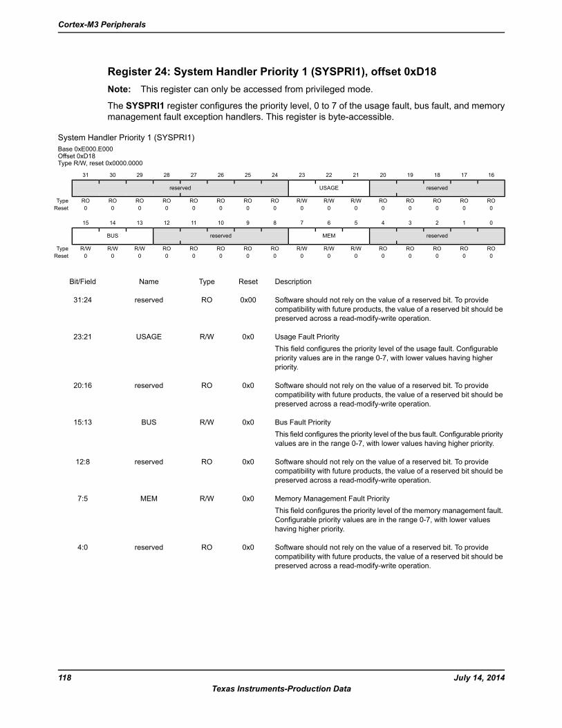
Register 24: System Handler Priority 1 (SYSPRI1), offset 0xD18Note: This register can only be accessed from privileged mode.
The SYSPRI1 register configures the priority level, 0 to 7 of the usage fault, bus fault, and memorymanagement fault exception handlers. This register is byte-accessible.
System Handler Priority 1 (SYSPRI1)Base 0xE000.E000Offset 0xD18Type R/W, reset 0x0000.0000
16171819202122232425262728293031
reservedUSAGEreserved
ROROROROROR/WR/WR/WROROROROROROROROType0000000000000000Reset
0123456789101112131415
reservedMEMreservedBUS
ROROROROROR/WR/WR/WROROROROROR/WR/WR/WType0000000000000000Reset
DescriptionResetTypeNameBit/Field
Software should not rely on the value of a reserved bit. To providecompatibility with future products, the value of a reserved bit should bepreserved across a read-modify-write operation.
0x00ROreserved31:24
Usage Fault PriorityThis field configures the priority level of the usage fault. Configurablepriority values are in the range 0-7, with lower values having higherpriority.
0x0R/WUSAGE23:21
Software should not rely on the value of a reserved bit. To providecompatibility with future products, the value of a reserved bit should bepreserved across a read-modify-write operation.
0x0ROreserved20:16
Bus Fault PriorityThis field configures the priority level of the bus fault. Configurable priorityvalues are in the range 0-7, with lower values having higher priority.
0x0R/WBUS15:13
Software should not rely on the value of a reserved bit. To providecompatibility with future products, the value of a reserved bit should bepreserved across a read-modify-write operation.
0x0ROreserved12:8
Memory Management Fault PriorityThis field configures the priority level of the memory management fault.Configurable priority values are in the range 0-7, with lower valueshaving higher priority.
0x0R/WMEM7:5
Software should not rely on the value of a reserved bit. To providecompatibility with future products, the value of a reserved bit should bepreserved across a read-modify-write operation.
0x0ROreserved4:0
July 14, 2014118Texas Instruments-Production Data
Cortex-M3 Peripherals
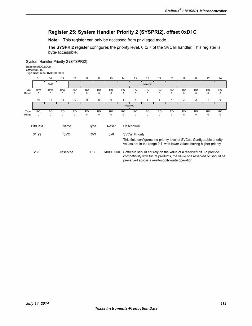
Register 25: System Handler Priority 2 (SYSPRI2), offset 0xD1CNote: This register can only be accessed from privileged mode.
The SYSPRI2 register configures the priority level, 0 to 7 of the SVCall handler. This register isbyte-accessible.
System Handler Priority 2 (SYSPRI2)Base 0xE000.E000Offset 0xD1CType R/W, reset 0x0000.0000
16171819202122232425262728293031
reservedSVC
ROROROROROROROROROROROROROR/WR/WR/WType0000000000000000Reset
0123456789101112131415
reserved
ROROROROROROROROROROROROROROROROType0000000000000000Reset
DescriptionResetTypeNameBit/Field
SVCall PriorityThis field configures the priority level of SVCall. Configurable priorityvalues are in the range 0-7, with lower values having higher priority.
0x0R/WSVC31:29
Software should not rely on the value of a reserved bit. To providecompatibility with future products, the value of a reserved bit should bepreserved across a read-modify-write operation.
0x000.0000ROreserved28:0
119July 14, 2014Texas Instruments-Production Data
Stellaris® LM3S601 Microcontroller
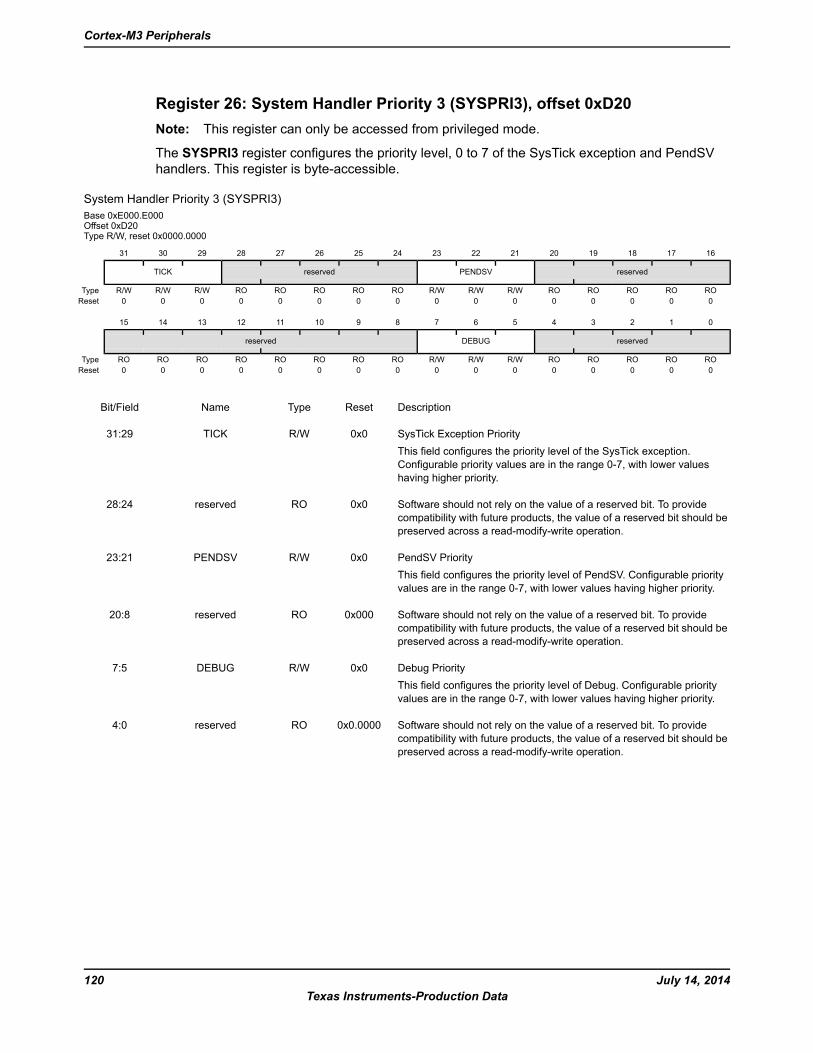
Register 26: System Handler Priority 3 (SYSPRI3), offset 0xD20Note: This register can only be accessed from privileged mode.
The SYSPRI3 register configures the priority level, 0 to 7 of the SysTick exception and PendSVhandlers. This register is byte-accessible.
System Handler Priority 3 (SYSPRI3)Base 0xE000.E000Offset 0xD20Type R/W, reset 0x0000.0000
16171819202122232425262728293031
reservedPENDSVreservedTICK
ROROROROROR/WR/WR/WROROROROROR/WR/WR/WType0000000000000000Reset
0123456789101112131415
reservedDEBUGreserved
ROROROROROR/WR/WR/WROROROROROROROROType0000000000000000Reset
DescriptionResetTypeNameBit/Field
SysTick Exception PriorityThis field configures the priority level of the SysTick exception.Configurable priority values are in the range 0-7, with lower valueshaving higher priority.
0x0R/WTICK31:29
Software should not rely on the value of a reserved bit. To providecompatibility with future products, the value of a reserved bit should bepreserved across a read-modify-write operation.
0x0ROreserved28:24
PendSV PriorityThis field configures the priority level of PendSV. Configurable priorityvalues are in the range 0-7, with lower values having higher priority.
0x0R/WPENDSV23:21
Software should not rely on the value of a reserved bit. To providecompatibility with future products, the value of a reserved bit should bepreserved across a read-modify-write operation.
0x000ROreserved20:8
Debug PriorityThis field configures the priority level of Debug. Configurable priorityvalues are in the range 0-7, with lower values having higher priority.
0x0R/WDEBUG7:5
Software should not rely on the value of a reserved bit. To providecompatibility with future products, the value of a reserved bit should bepreserved across a read-modify-write operation.
0x0.0000ROreserved4:0
July 14, 2014120Texas Instruments-Production Data
Cortex-M3 Peripherals
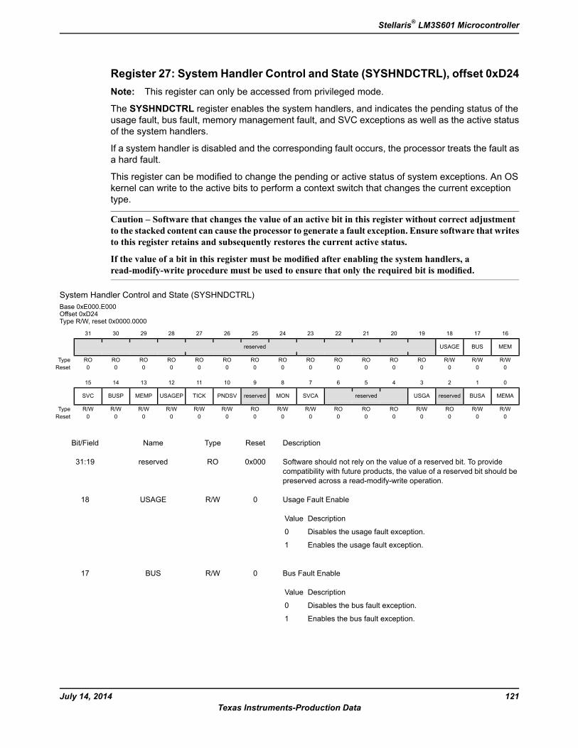
Register 27: System Handler Control and State (SYSHNDCTRL), offset 0xD24Note: This register can only be accessed from privileged mode.
The SYSHNDCTRL register enables the system handlers, and indicates the pending status of theusage fault, bus fault, memory management fault, and SVC exceptions as well as the active statusof the system handlers.
If a system handler is disabled and the corresponding fault occurs, the processor treats the fault asa hard fault.
This register can be modified to change the pending or active status of system exceptions. An OSkernel can write to the active bits to perform a context switch that changes the current exceptiontype.
Caution – Software that changes the value of an active bit in this register without correct adjustmentto the stacked content can cause the processor to generate a fault exception. Ensure software that writesto this register retains and subsequently restores the current active status.
If the value of a bit in this register must be modified after enabling the system handlers, aread-modify-write procedure must be used to ensure that only the required bit is modified.
System Handler Control and State (SYSHNDCTRL)Base 0xE000.E000Offset 0xD24Type R/W, reset 0x0000.0000
16171819202122232425262728293031
MEMBUSUSAGEreserved
R/WR/WR/WROROROROROROROROROROROROROType0000000000000000Reset
0123456789101112131415
MEMABUSAreservedUSGAreservedSVCAMONreservedPNDSVTICKUSAGEPMEMPBUSPSVC
R/WR/WROR/WROROROR/WR/WROR/WR/WR/WR/WR/WR/WType0000000000000000Reset
DescriptionResetTypeNameBit/Field
Software should not rely on the value of a reserved bit. To providecompatibility with future products, the value of a reserved bit should bepreserved across a read-modify-write operation.
0x000ROreserved31:19
Usage Fault Enable
DescriptionValue
Disables the usage fault exception.0
Enables the usage fault exception.1
0R/WUSAGE18
Bus Fault Enable
DescriptionValue
Disables the bus fault exception.0
Enables the bus fault exception.1
0R/WBUS17
121July 14, 2014Texas Instruments-Production Data
Stellaris® LM3S601 Microcontroller
DescriptionResetTypeNameBit/Field
Memory Management Fault Enable
DescriptionValue
Disables the memory management fault exception.0
Enables the memory management fault exception.1
0R/WMEM16
SVC Call Pending
DescriptionValue
An SVC call exception is not pending.0
An SVC call exception is pending.1
This bit can be modified to change the pending status of the SVC callexception.
0R/WSVC15
Bus Fault Pending
DescriptionValue
A bus fault exception is not pending.0
A bus fault exception is pending.1
This bit can be modified to change the pending status of the bus faultexception.
0R/WBUSP14
Memory Management Fault Pending
DescriptionValue
A memory management fault exception is not pending.0
A memory management fault exception is pending.1
This bit can be modified to change the pending status of the memorymanagement fault exception.
0R/WMEMP13
Usage Fault Pending
DescriptionValue
A usage fault exception is not pending.0
A usage fault exception is pending.1
This bit can be modified to change the pending status of the usage faultexception.
0R/WUSAGEP12
SysTick Exception Active
DescriptionValue
A SysTick exception is not active.0
A SysTick exception is active.1
This bit can be modified to change the active status of the SysTickexception, however, see the Caution above before setting this bit.
0R/WTICK11
July 14, 2014122Texas Instruments-Production Data
Cortex-M3 Peripherals
DescriptionResetTypeNameBit/Field
PendSV Exception Active
DescriptionValue
A PendSV exception is not active.0
A PendSV exception is active.1
This bit can be modified to change the active status of the PendSVexception, however, see the Caution above before setting this bit.
0R/WPNDSV10
Software should not rely on the value of a reserved bit. To providecompatibility with future products, the value of a reserved bit should bepreserved across a read-modify-write operation.
0ROreserved9
Debug Monitor Active
DescriptionValue
The Debug monitor is not active.0
The Debug monitor is active.1
0R/WMON8
SVC Call Active
DescriptionValue
SVC call is not active.0
SVC call is active.1
This bit can be modified to change the active status of the SVC callexception, however, see the Caution above before setting this bit.
0R/WSVCA7
Software should not rely on the value of a reserved bit. To providecompatibility with future products, the value of a reserved bit should bepreserved across a read-modify-write operation.
0x0ROreserved6:4
Usage Fault Active
DescriptionValue
Usage fault is not active.0
Usage fault is active.1
This bit can be modified to change the active status of the usage faultexception, however, see the Caution above before setting this bit.
0R/WUSGA3
Software should not rely on the value of a reserved bit. To providecompatibility with future products, the value of a reserved bit should bepreserved across a read-modify-write operation.
0ROreserved2
Bus Fault Active
DescriptionValue
Bus fault is not active.0
Bus fault is active.1
This bit can be modified to change the active status of the bus faultexception, however, see the Caution above before setting this bit.
0R/WBUSA1
123July 14, 2014Texas Instruments-Production Data
Stellaris® LM3S601 Microcontroller
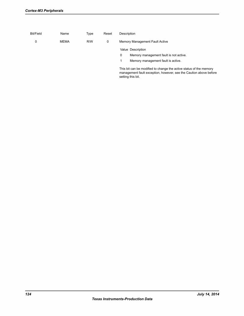
DescriptionResetTypeNameBit/Field
Memory Management Fault Active
DescriptionValue
Memory management fault is not active.0
Memory management fault is active.1
This bit can be modified to change the active status of the memorymanagement fault exception, however, see the Caution above beforesetting this bit.
0R/WMEMA0
July 14, 2014124Texas Instruments-Production Data
Cortex-M3 Peripherals
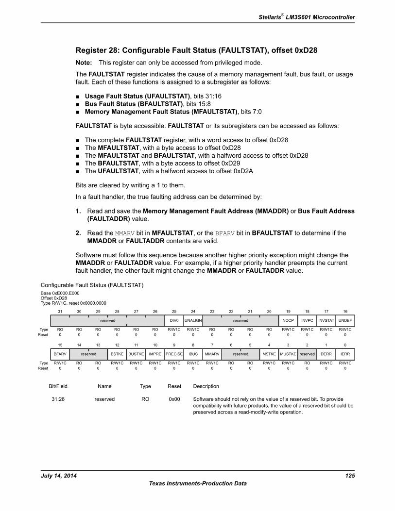
Register 28: Configurable Fault Status (FAULTSTAT), offset 0xD28Note: This register can only be accessed from privileged mode.
The FAULTSTAT register indicates the cause of a memory management fault, bus fault, or usagefault. Each of these functions is assigned to a subregister as follows:
Usage Fault Status (UFAULTSTAT), bits 31:16 Bus Fault Status (BFAULTSTAT), bits 15:8 Memory Management Fault Status (MFAULTSTAT), bits 7:0
FAULTSTAT is byte accessible. FAULTSTAT or its subregisters can be accessed as follows:
The complete FAULTSTAT register, with a word access to offset 0xD28 The MFAULTSTAT, with a byte access to offset 0xD28 The MFAULTSTAT and BFAULTSTAT, with a halfword access to offset 0xD28 The BFAULTSTAT, with a byte access to offset 0xD29 The UFAULTSTAT, with a halfword access to offset 0xD2A
Bits are cleared by writing a 1 to them.
In a fault handler, the true faulting address can be determined by:
1. Read and save the Memory Management Fault Address (MMADDR) or Bus Fault Address(FAULTADDR) value.
2. Read the MMARV bit in MFAULTSTAT, or the BFARV bit in BFAULTSTAT to determine if theMMADDR or FAULTADDR contents are valid.
Software must follow this sequence because another higher priority exception might change theMMADDR or FAULTADDR value. For example, if a higher priority handler preempts the currentfault handler, the other fault might change the MMADDR or FAULTADDR value.
Configurable Fault Status (FAULTSTAT)Base 0xE000.E000Offset 0xD28Type R/W1C, reset 0x0000.0000
16171819202122232425262728293031
UNDEFINVSTATINVPCNOCPreservedUNALIGNDIV0reserved
R/W1CR/W1CR/W1CR/W1CROROROROR/W1CR/W1CROROROROROROType0000000000000000Reset
0123456789101112131415
IERRDERRreservedMUSTKEMSTKEreservedMMARVIBUSPRECISEIMPREBUSTKEBSTKEreservedBFARV
R/W1CR/W1CROR/W1CR/W1CROROR/W1CR/W1CR/W1CR/W1CR/W1CR/W1CROROR/W1CType0000000000000000Reset
DescriptionResetTypeNameBit/Field
Software should not rely on the value of a reserved bit. To providecompatibility with future products, the value of a reserved bit should bepreserved across a read-modify-write operation.
0x00ROreserved31:26
125July 14, 2014Texas Instruments-Production Data
Stellaris® LM3S601 Microcontroller
DescriptionResetTypeNameBit/Field
Divide-by-Zero Usage Fault
DescriptionValue
No divide-by-zero fault has occurred, or divide-by-zero trappingis not enabled.
0
The processor has executed an SDIV or UDIV instruction witha divisor of 0.
1
When this bit is set, the PC value stacked for the exception return pointsto the instruction that performed the divide by zero.Trapping on divide-by-zero is enabled by setting the DIV0 bit in theConfiguration and Control (CFGCTRL) register (see page 116).This bit is cleared by writing a 1 to it.
0R/W1CDIV025
Unaligned Access Usage Fault
DescriptionValue
No unaligned access fault has occurred, or unaligned accesstrapping is not enabled.
0
The processor has made an unaligned memory access.1
Unaligned LDM, STM, LDRD, and STRD instructions always faultregardless of the configuration of this bit.Trapping on unaligned access is enabled by setting the UNALIGNED bitin the CFGCTRL register (see page 116).This bit is cleared by writing a 1 to it.
0R/W1CUNALIGN24
Software should not rely on the value of a reserved bit. To providecompatibility with future products, the value of a reserved bit should bepreserved across a read-modify-write operation.
0x00ROreserved23:20
No Coprocessor Usage Fault
DescriptionValue
A usage fault has not been caused by attempting to access acoprocessor.
0
The processor has attempted to access a coprocessor.1
This bit is cleared by writing a 1 to it.
0R/W1CNOCP19
Invalid PC Load Usage Fault
DescriptionValue
A usage fault has not been caused by attempting to load aninvalid PC value.
0
The processor has attempted an illegal load of EXC_RETURNto the PC as a result of an invalid context or an invalidEXC_RETURN value.
1
When this bit is set, the PC value stacked for the exception return pointsto the instruction that tried to perform the illegal load of the PC.This bit is cleared by writing a 1 to it.
0R/W1CINVPC18
July 14, 2014126Texas Instruments-Production Data
Cortex-M3 Peripherals
DescriptionResetTypeNameBit/Field
Invalid State Usage Fault
DescriptionValue
A usage fault has not been caused by an invalid state.0
The processor has attempted to execute an instruction thatmakes illegal use of the EPSR register.
1
When this bit is set, the PC value stacked for the exception return pointsto the instruction that attempted the illegal use of the ExecutionProgram Status Register (EPSR) register.This bit is not set if an undefined instruction uses the EPSR register.This bit is cleared by writing a 1 to it.
0R/W1CINVSTAT17
Undefined Instruction Usage Fault
DescriptionValue
A usage fault has not been caused by an undefined instruction.0
The processor has attempted to execute an undefinedinstruction.
1
When this bit is set, the PC value stacked for the exception return pointsto the undefined instruction.An undefined instruction is an instruction that the processor cannotdecode.This bit is cleared by writing a 1 to it.
0R/W1CUNDEF16
Bus Fault Address Register Valid
DescriptionValue
The value in the Bus Fault Address (FAULTADDR) registeris not a valid fault address.
0
The FAULTADDR register is holding a valid fault address.1
This bit is set after a bus fault, where the address is known. Other faultscan clear this bit, such as a memory management fault occurring later.If a bus fault occurs and is escalated to a hard fault because of priority,the hard fault handler must clear this bit. This action prevents problemsif returning to a stacked active bus fault handler whose FAULTADDRregister value has been overwritten.This bit is cleared by writing a 1 to it.
0R/W1CBFARV15
Software should not rely on the value of a reserved bit. To providecompatibility with future products, the value of a reserved bit should bepreserved across a read-modify-write operation.
0ROreserved14:13
127July 14, 2014Texas Instruments-Production Data
Stellaris® LM3S601 Microcontroller
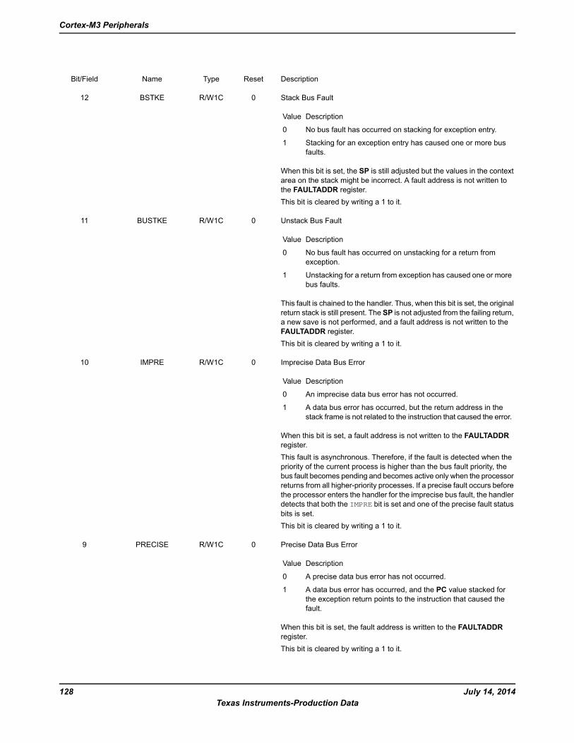
DescriptionResetTypeNameBit/Field
Stack Bus Fault
DescriptionValue
No bus fault has occurred on stacking for exception entry.0
Stacking for an exception entry has caused one or more busfaults.
1
When this bit is set, the SP is still adjusted but the values in the contextarea on the stack might be incorrect. A fault address is not written tothe FAULTADDR register.This bit is cleared by writing a 1 to it.
0R/W1CBSTKE12
Unstack Bus Fault
DescriptionValue
No bus fault has occurred on unstacking for a return fromexception.
0
Unstacking for a return from exception has caused one or morebus faults.
1
This fault is chained to the handler. Thus, when this bit is set, the originalreturn stack is still present. The SP is not adjusted from the failing return,a new save is not performed, and a fault address is not written to theFAULTADDR register.This bit is cleared by writing a 1 to it.
0R/W1CBUSTKE11
Imprecise Data Bus Error
DescriptionValue
An imprecise data bus error has not occurred.0
A data bus error has occurred, but the return address in thestack frame is not related to the instruction that caused the error.
1
When this bit is set, a fault address is not written to the FAULTADDRregister.This fault is asynchronous. Therefore, if the fault is detected when thepriority of the current process is higher than the bus fault priority, thebus fault becomes pending and becomes active only when the processorreturns from all higher-priority processes. If a precise fault occurs beforethe processor enters the handler for the imprecise bus fault, the handlerdetects that both the IMPRE bit is set and one of the precise fault statusbits is set.This bit is cleared by writing a 1 to it.
0R/W1CIMPRE10
Precise Data Bus Error
DescriptionValue
A precise data bus error has not occurred.0
A data bus error has occurred, and the PC value stacked forthe exception return points to the instruction that caused thefault.
1
When this bit is set, the fault address is written to the FAULTADDRregister.This bit is cleared by writing a 1 to it.
0R/W1CPRECISE9
July 14, 2014128Texas Instruments-Production Data
Cortex-M3 Peripherals
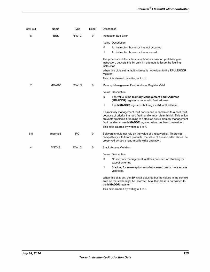
DescriptionResetTypeNameBit/Field
Instruction Bus Error
DescriptionValue
An instruction bus error has not occurred.0
An instruction bus error has occurred.1
The processor detects the instruction bus error on prefetching aninstruction, but sets this bit only if it attempts to issue the faultinginstruction.When this bit is set, a fault address is not written to the FAULTADDRregister.This bit is cleared by writing a 1 to it.
0R/W1CIBUS8
Memory Management Fault Address Register Valid
DescriptionValue
The value in the Memory Management Fault Address(MMADDR) register is not a valid fault address.
0
The MMADDR register is holding a valid fault address.1
If a memory management fault occurs and is escalated to a hard faultbecause of priority, the hard fault handler must clear this bit. This actionprevents problems if returning to a stacked active memory managementfault handler whose MMADDR register value has been overwritten.This bit is cleared by writing a 1 to it.
0R/W1CMMARV7
Software should not rely on the value of a reserved bit. To providecompatibility with future products, the value of a reserved bit should bepreserved across a read-modify-write operation.
0ROreserved6:5
Stack Access Violation
DescriptionValue
No memory management fault has occurred on stacking forexception entry.
0
Stacking for an exception entry has caused one or more accessviolations.
1
When this bit is set, the SP is still adjusted but the values in the contextarea on the stack might be incorrect. A fault address is not written tothe MMADDR register.This bit is cleared by writing a 1 to it.
0R/W1CMSTKE4
129July 14, 2014Texas Instruments-Production Data
Stellaris® LM3S601 Microcontroller
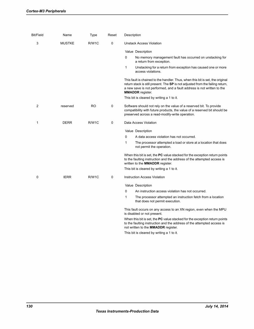
DescriptionResetTypeNameBit/Field
Unstack Access Violation
DescriptionValue
No memory management fault has occurred on unstacking fora return from exception.
0
Unstacking for a return from exception has caused one or moreaccess violations.
1
This fault is chained to the handler. Thus, when this bit is set, the originalreturn stack is still present. The SP is not adjusted from the failing return,a new save is not performed, and a fault address is not written to theMMADDR register.This bit is cleared by writing a 1 to it.
0R/W1CMUSTKE3
Software should not rely on the value of a reserved bit. To providecompatibility with future products, the value of a reserved bit should bepreserved across a read-modify-write operation.
0ROreserved2
Data Access Violation
DescriptionValue
A data access violation has not occurred.0
The processor attempted a load or store at a location that doesnot permit the operation.
1
When this bit is set, the PC value stacked for the exception return pointsto the faulting instruction and the address of the attempted access iswritten to the MMADDR register.This bit is cleared by writing a 1 to it.
0R/W1CDERR1
Instruction Access Violation
DescriptionValue
An instruction access violation has not occurred.0
The processor attempted an instruction fetch from a locationthat does not permit execution.
1
This fault occurs on any access to an XN region, even when the MPUis disabled or not present.When this bit is set, the PC value stacked for the exception return pointsto the faulting instruction and the address of the attempted access isnot written to the MMADDR register.This bit is cleared by writing a 1 to it.
0R/W1CIERR0
July 14, 2014130Texas Instruments-Production Data
Cortex-M3 Peripherals
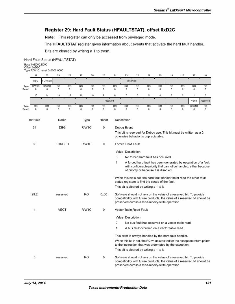
Register 29: Hard Fault Status (HFAULTSTAT), offset 0xD2CNote: This register can only be accessed from privileged mode.
The HFAULTSTAT register gives information about events that activate the hard fault handler.
Bits are cleared by writing a 1 to them.
Hard Fault Status (HFAULTSTAT)Base 0xE000.E000Offset 0xD2CType R/W1C, reset 0x0000.0000
16171819202122232425262728293031
reservedFORCEDDBG
ROROROROROROROROROROROROROROR/W1CR/W1CType0000000000000000Reset
0123456789101112131415
reservedVECTreserved
ROR/W1CROROROROROROROROROROROROROROType0000000000000000Reset
DescriptionResetTypeNameBit/Field
Debug EventThis bit is reserved for Debug use. This bit must be written as a 0,otherwise behavior is unpredictable.
0R/W1CDBG31
Forced Hard Fault
DescriptionValue
No forced hard fault has occurred.0
A forced hard fault has been generated by escalation of a faultwith configurable priority that cannot be handled, either becauseof priority or because it is disabled.
1
When this bit is set, the hard fault handler must read the other faultstatus registers to find the cause of the fault.This bit is cleared by writing a 1 to it.
0R/W1CFORCED30
Software should not rely on the value of a reserved bit. To providecompatibility with future products, the value of a reserved bit should bepreserved across a read-modify-write operation.
0x00ROreserved29:2
Vector Table Read Fault
DescriptionValue
No bus fault has occurred on a vector table read.0
A bus fault occurred on a vector table read.1
This error is always handled by the hard fault handler.When this bit is set, the PC value stacked for the exception return pointsto the instruction that was preempted by the exception.This bit is cleared by writing a 1 to it.
0R/W1CVECT1
Software should not rely on the value of a reserved bit. To providecompatibility with future products, the value of a reserved bit should bepreserved across a read-modify-write operation.
0ROreserved0
131July 14, 2014Texas Instruments-Production Data
Stellaris® LM3S601 Microcontroller
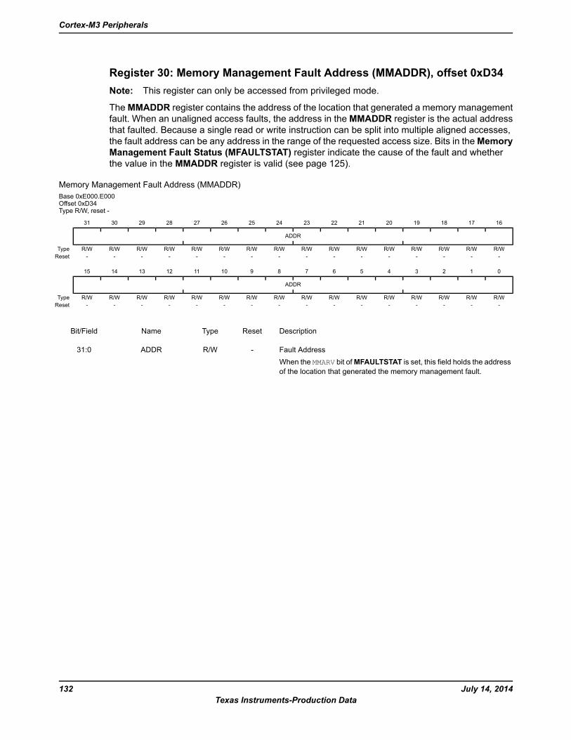
Register 30: Memory Management Fault Address (MMADDR), offset 0xD34Note: This register can only be accessed from privileged mode.
TheMMADDR register contains the address of the location that generated a memory managementfault. When an unaligned access faults, the address in theMMADDR register is the actual addressthat faulted. Because a single read or write instruction can be split into multiple aligned accesses,the fault address can be any address in the range of the requested access size. Bits in theMemoryManagement Fault Status (MFAULTSTAT) register indicate the cause of the fault and whetherthe value in the MMADDR register is valid (see page 125).
Memory Management Fault Address (MMADDR)Base 0xE000.E000Offset 0xD34Type R/W, reset -
16171819202122232425262728293031
ADDR
R/WR/WR/WR/WR/WR/WR/WR/WR/WR/WR/WR/WR/WR/WR/WR/WType----------------Reset
0123456789101112131415
ADDR
R/WR/WR/WR/WR/WR/WR/WR/WR/WR/WR/WR/WR/WR/WR/WR/WType----------------Reset
DescriptionResetTypeNameBit/Field
Fault AddressWhen the MMARV bit ofMFAULTSTAT is set, this field holds the addressof the location that generated the memory management fault.
-R/WADDR31:0
July 14, 2014132Texas Instruments-Production Data
Cortex-M3 Peripherals
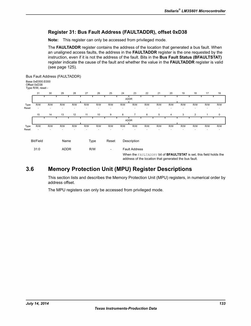
Register 31: Bus Fault Address (FAULTADDR), offset 0xD38Note: This register can only be accessed from privileged mode.
The FAULTADDR register contains the address of the location that generated a bus fault. Whenan unaligned access faults, the address in the FAULTADDR register is the one requested by theinstruction, even if it is not the address of the fault. Bits in the Bus Fault Status (BFAULTSTAT)register indicate the cause of the fault and whether the value in the FAULTADDR register is valid(see page 125).
Bus Fault Address (FAULTADDR)Base 0xE000.E000Offset 0xD38Type R/W, reset -
16171819202122232425262728293031
ADDR
R/WR/WR/WR/WR/WR/WR/WR/WR/WR/WR/WR/WR/WR/WR/WR/WType----------------Reset
0123456789101112131415
ADDR
R/WR/WR/WR/WR/WR/WR/WR/WR/WR/WR/WR/WR/WR/WR/WR/WType----------------Reset
DescriptionResetTypeNameBit/Field
Fault AddressWhen the FAULTADDRV bit of BFAULTSTAT is set, this field holds theaddress of the location that generated the bus fault.
-R/WADDR31:0
3.6 Memory Protection Unit (MPU) Register DescriptionsThis section lists and describes the Memory Protection Unit (MPU) registers, in numerical order byaddress offset.
The MPU registers can only be accessed from privileged mode.
133July 14, 2014Texas Instruments-Production Data
Stellaris® LM3S601 Microcontroller
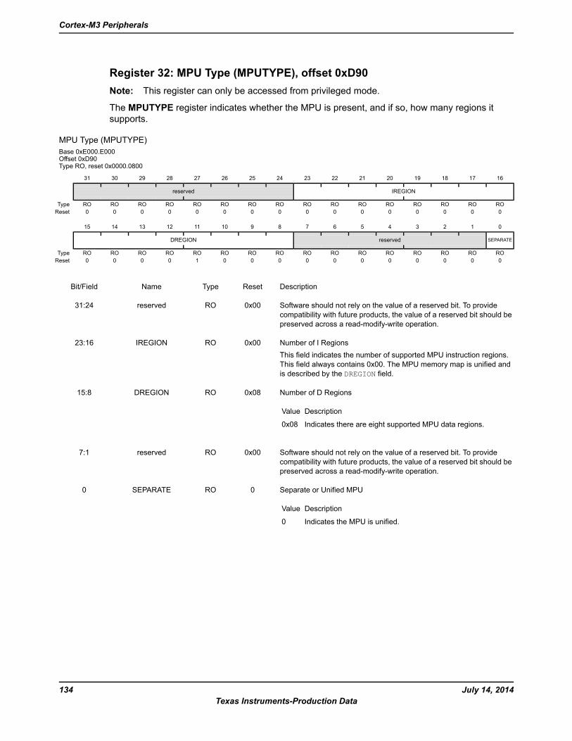
Register 32: MPU Type (MPUTYPE), offset 0xD90Note: This register can only be accessed from privileged mode.
The MPUTYPE register indicates whether the MPU is present, and if so, how many regions itsupports.
MPU Type (MPUTYPE)Base 0xE000.E000Offset 0xD90Type RO, reset 0x0000.0800
16171819202122232425262728293031
IREGIONreserved
ROROROROROROROROROROROROROROROROType0000000000000000Reset
0123456789101112131415
SEPARATEreservedDREGION
ROROROROROROROROROROROROROROROROType0000000000010000Reset
DescriptionResetTypeNameBit/Field
Software should not rely on the value of a reserved bit. To providecompatibility with future products, the value of a reserved bit should bepreserved across a read-modify-write operation.
0x00ROreserved31:24
Number of I RegionsThis field indicates the number of supported MPU instruction regions.This field always contains 0x00. The MPU memory map is unified andis described by the DREGION field.
0x00ROIREGION23:16
Number of D Regions
DescriptionValue
Indicates there are eight supported MPU data regions.0x08
0x08RODREGION15:8
Software should not rely on the value of a reserved bit. To providecompatibility with future products, the value of a reserved bit should bepreserved across a read-modify-write operation.
0x00ROreserved7:1
Separate or Unified MPU
DescriptionValue
Indicates the MPU is unified.0
0ROSEPARATE0
July 14, 2014134Texas Instruments-Production Data
Cortex-M3 Peripherals
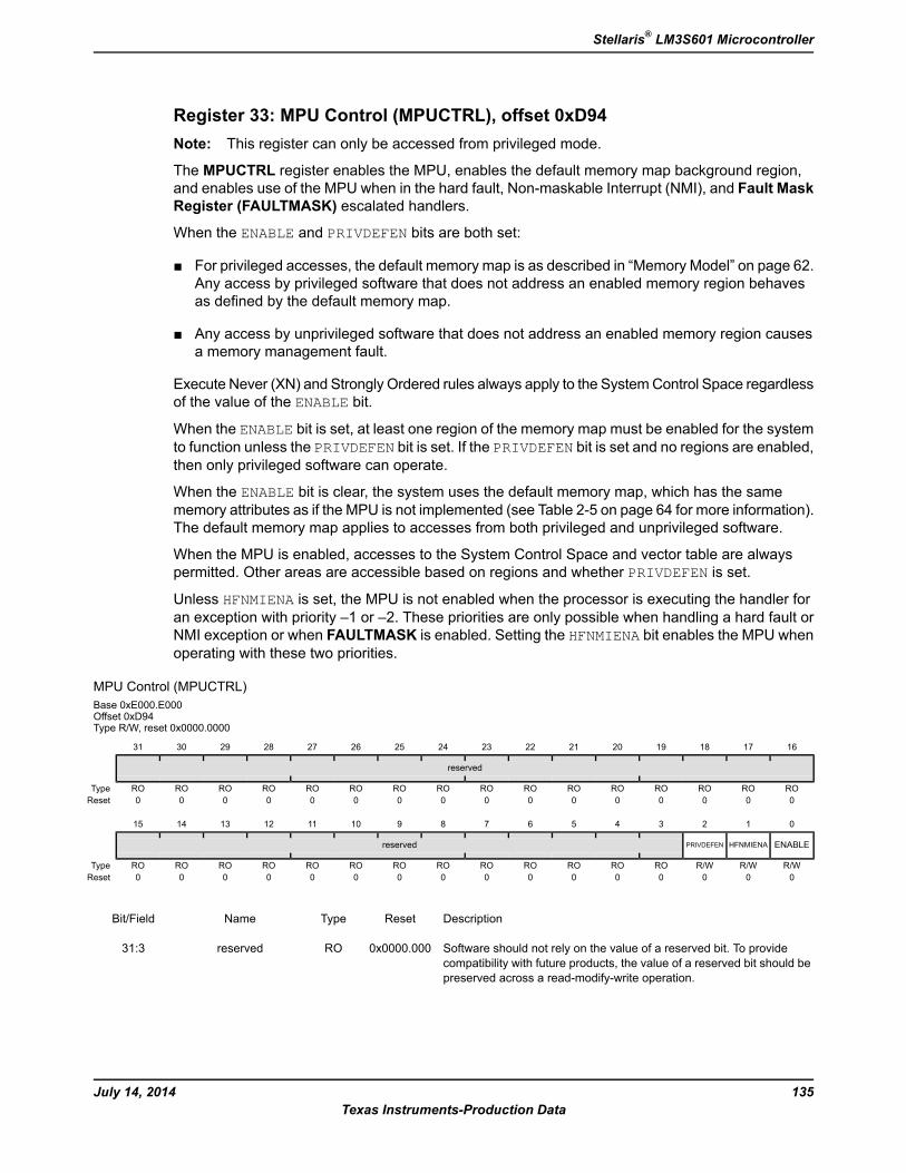
Register 33: MPU Control (MPUCTRL), offset 0xD94Note: This register can only be accessed from privileged mode.
The MPUCTRL register enables the MPU, enables the default memory map background region,and enables use of the MPU when in the hard fault, Non-maskable Interrupt (NMI), and Fault MaskRegister (FAULTMASK) escalated handlers.
When the ENABLE and PRIVDEFEN bits are both set:
For privileged accesses, the default memory map is as described in “Memory Model” on page 62.Any access by privileged software that does not address an enabled memory region behavesas defined by the default memory map.
Any access by unprivileged software that does not address an enabled memory region causesa memory management fault.
Execute Never (XN) and Strongly Ordered rules always apply to the SystemControl Space regardlessof the value of the ENABLE bit.
When the ENABLE bit is set, at least one region of the memory map must be enabled for the systemto function unless the PRIVDEFEN bit is set. If the PRIVDEFEN bit is set and no regions are enabled,then only privileged software can operate.
When the ENABLE bit is clear, the system uses the default memory map, which has the samememory attributes as if the MPU is not implemented (see Table 2-5 on page 64 for more information).The default memory map applies to accesses from both privileged and unprivileged software.
When the MPU is enabled, accesses to the System Control Space and vector table are alwayspermitted. Other areas are accessible based on regions and whether PRIVDEFEN is set.
Unless HFNMIENA is set, the MPU is not enabled when the processor is executing the handler foran exception with priority –1 or –2. These priorities are only possible when handling a hard fault orNMI exception or when FAULTMASK is enabled. Setting the HFNMIENA bit enables the MPU whenoperating with these two priorities.
MPU Control (MPUCTRL)Base 0xE000.E000Offset 0xD94Type R/W, reset 0x0000.0000
16171819202122232425262728293031
reserved
ROROROROROROROROROROROROROROROROType0000000000000000Reset
0123456789101112131415
ENABLEHFNMIENAPRIVDEFENreserved
R/WR/WR/WROROROROROROROROROROROROROType0000000000000000Reset
DescriptionResetTypeNameBit/Field
Software should not rely on the value of a reserved bit. To providecompatibility with future products, the value of a reserved bit should bepreserved across a read-modify-write operation.
0x0000.000ROreserved31:3
135July 14, 2014Texas Instruments-Production Data
Stellaris® LM3S601 Microcontroller
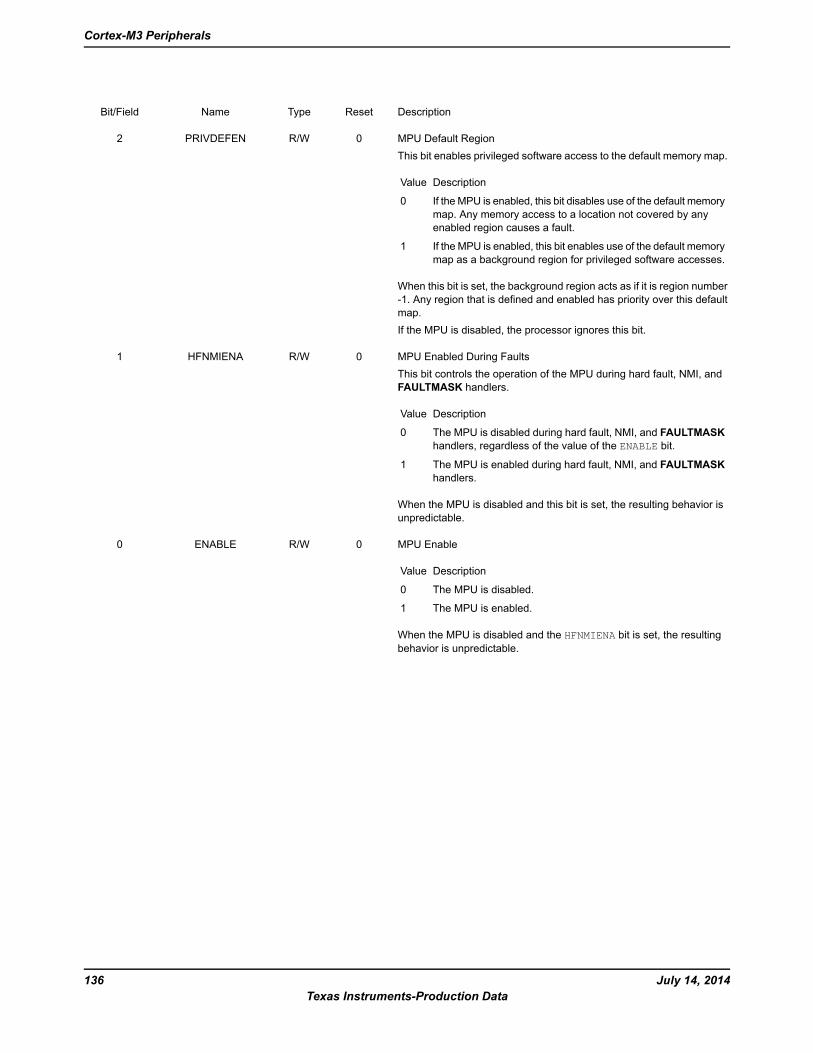
DescriptionResetTypeNameBit/Field
MPU Default RegionThis bit enables privileged software access to the default memory map.
DescriptionValue
If the MPU is enabled, this bit disables use of the default memorymap. Any memory access to a location not covered by anyenabled region causes a fault.
0
If the MPU is enabled, this bit enables use of the default memorymap as a background region for privileged software accesses.
1
When this bit is set, the background region acts as if it is region number-1. Any region that is defined and enabled has priority over this defaultmap.If the MPU is disabled, the processor ignores this bit.
0R/WPRIVDEFEN2
MPU Enabled During FaultsThis bit controls the operation of the MPU during hard fault, NMI, andFAULTMASK handlers.
DescriptionValue
The MPU is disabled during hard fault, NMI, and FAULTMASKhandlers, regardless of the value of the ENABLE bit.
0
The MPU is enabled during hard fault, NMI, and FAULTMASKhandlers.
1
When the MPU is disabled and this bit is set, the resulting behavior isunpredictable.
0R/WHFNMIENA1
MPU Enable
DescriptionValue
The MPU is disabled.0
The MPU is enabled.1
When the MPU is disabled and the HFNMIENA bit is set, the resultingbehavior is unpredictable.
0R/WENABLE0
July 14, 2014136Texas Instruments-Production Data
Cortex-M3 Peripherals
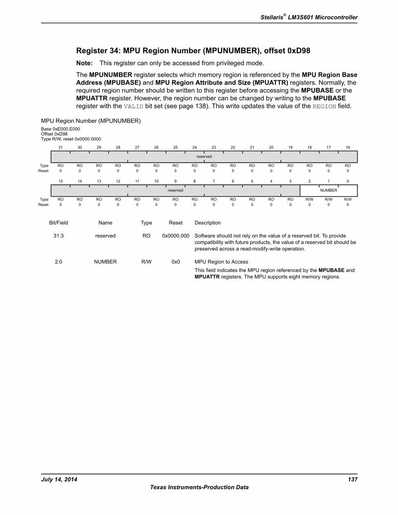
Register 34: MPU Region Number (MPUNUMBER), offset 0xD98Note: This register can only be accessed from privileged mode.
The MPUNUMBER register selects which memory region is referenced by the MPU Region BaseAddress (MPUBASE) and MPU Region Attribute and Size (MPUATTR) registers. Normally, therequired region number should be written to this register before accessing the MPUBASE or theMPUATTR register. However, the region number can be changed by writing to the MPUBASEregister with the VALID bit set (see page 138). This write updates the value of the REGION field.
MPU Region Number (MPUNUMBER)Base 0xE000.E000Offset 0xD98Type R/W, reset 0x0000.0000
16171819202122232425262728293031
reserved
ROROROROROROROROROROROROROROROROType0000000000000000Reset
0123456789101112131415
NUMBERreserved
R/WR/WR/WROROROROROROROROROROROROROType0000000000000000Reset
DescriptionResetTypeNameBit/Field
Software should not rely on the value of a reserved bit. To providecompatibility with future products, the value of a reserved bit should bepreserved across a read-modify-write operation.
0x0000.000ROreserved31:3
MPU Region to AccessThis field indicates the MPU region referenced by the MPUBASE andMPUATTR registers. The MPU supports eight memory regions.
0x0R/WNUMBER2:0
137July 14, 2014Texas Instruments-Production Data
Stellaris® LM3S601 Microcontroller
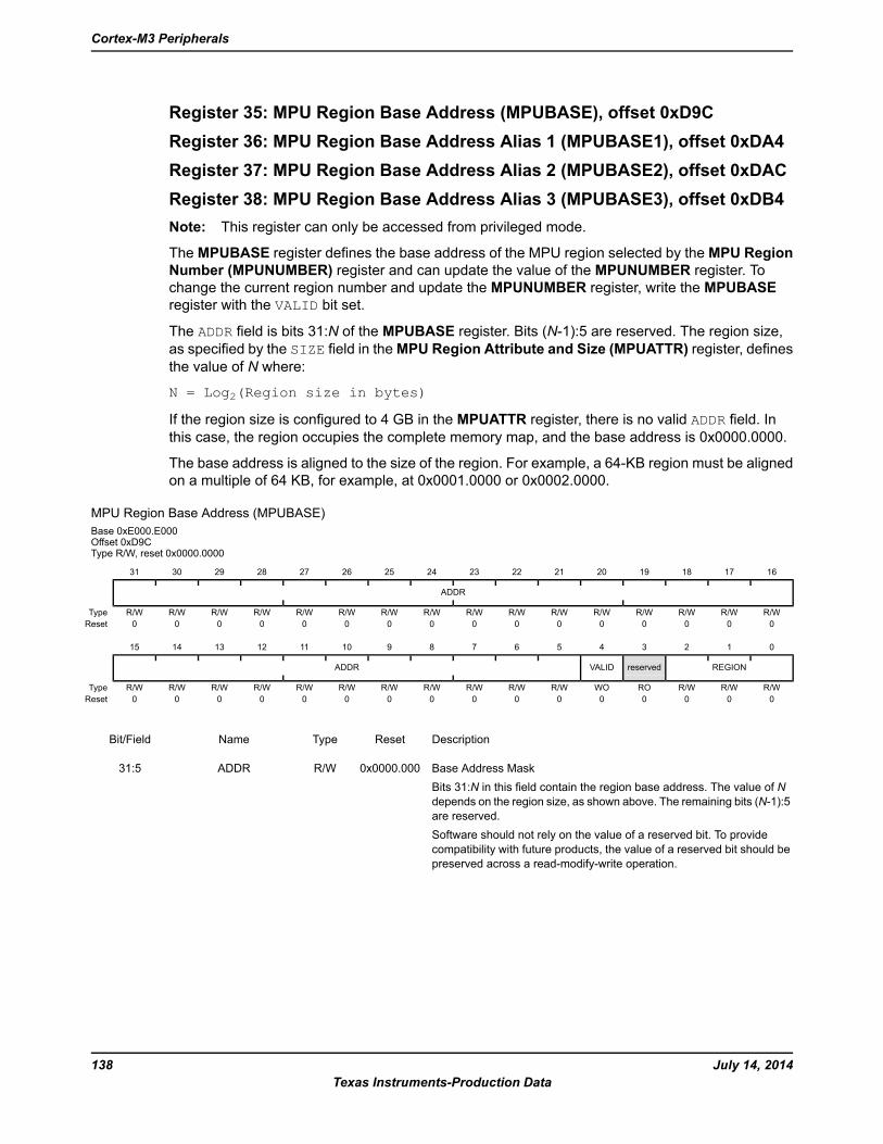
Register 35: MPU Region Base Address (MPUBASE), offset 0xD9CRegister 36: MPU Region Base Address Alias 1 (MPUBASE1), offset 0xDA4Register 37: MPU Region Base Address Alias 2 (MPUBASE2), offset 0xDACRegister 38: MPU Region Base Address Alias 3 (MPUBASE3), offset 0xDB4Note: This register can only be accessed from privileged mode.
The MPUBASE register defines the base address of the MPU region selected by the MPU RegionNumber (MPUNUMBER) register and can update the value of the MPUNUMBER register. Tochange the current region number and update the MPUNUMBER register, write the MPUBASEregister with the VALID bit set.
The ADDR field is bits 31:N of the MPUBASE register. Bits (N-1):5 are reserved. The region size,as specified by the SIZE field in theMPU Region Attribute and Size (MPUATTR) register, definesthe value of N where:
N = Log2(Region size in bytes)
If the region size is configured to 4 GB in the MPUATTR register, there is no valid ADDR field. Inthis case, the region occupies the complete memory map, and the base address is 0x0000.0000.
The base address is aligned to the size of the region. For example, a 64-KB region must be alignedon a multiple of 64 KB, for example, at 0x0001.0000 or 0x0002.0000.
MPU Region Base Address (MPUBASE)Base 0xE000.E000Offset 0xD9CType R/W, reset 0x0000.0000
16171819202122232425262728293031
ADDR
R/WR/WR/WR/WR/WR/WR/WR/WR/WR/WR/WR/WR/WR/WR/WR/WType0000000000000000Reset
0123456789101112131415
REGIONreservedVALIDADDR
R/WR/WR/WROWOR/WR/WR/WR/WR/WR/WR/WR/WR/WR/WR/WType0000000000000000Reset
DescriptionResetTypeNameBit/Field
Base Address MaskBits 31:N in this field contain the region base address. The value of Ndepends on the region size, as shown above. The remaining bits (N-1):5are reserved.Software should not rely on the value of a reserved bit. To providecompatibility with future products, the value of a reserved bit should bepreserved across a read-modify-write operation.
0x0000.000R/WADDR31:5
July 14, 2014138Texas Instruments-Production Data
Cortex-M3 Peripherals
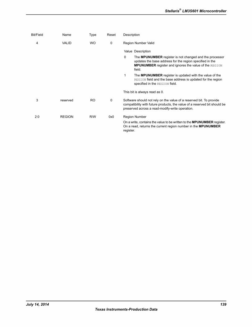
DescriptionResetTypeNameBit/Field
Region Number Valid
DescriptionValue
The MPUNUMBER register is not changed and the processorupdates the base address for the region specified in theMPUNUMBER register and ignores the value of the REGIONfield.
0
The MPUNUMBER register is updated with the value of theREGION field and the base address is updated for the regionspecified in the REGION field.
1
This bit is always read as 0.
0WOVALID4
Software should not rely on the value of a reserved bit. To providecompatibility with future products, the value of a reserved bit should bepreserved across a read-modify-write operation.
0ROreserved3
Region NumberOn a write, contains the value to be written to theMPUNUMBER register.On a read, returns the current region number in the MPUNUMBERregister.
0x0R/WREGION2:0
139July 14, 2014Texas Instruments-Production Data
Stellaris® LM3S601 Microcontroller
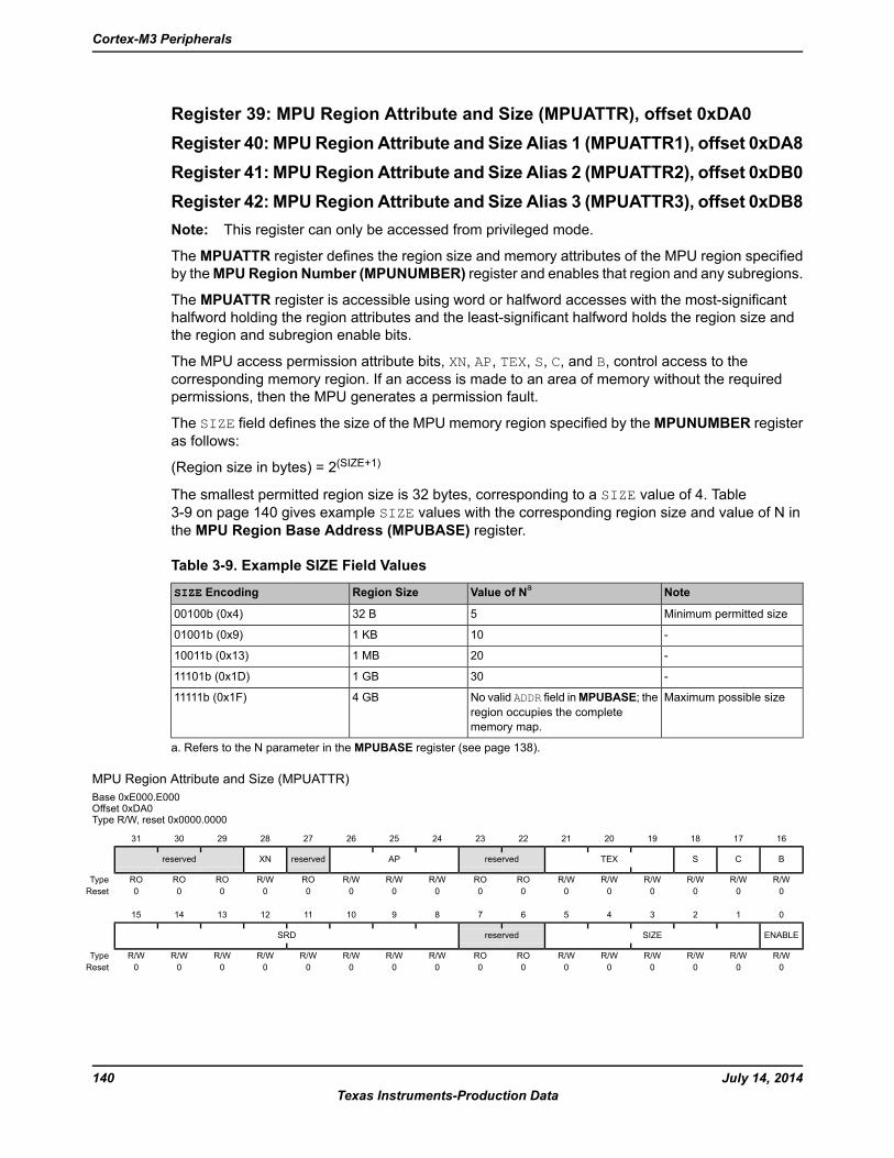
Register 39: MPU Region Attribute and Size (MPUATTR), offset 0xDA0Register 40: MPURegion Attribute and Size Alias 1 (MPUATTR1), offset 0xDA8Register 41: MPURegion Attribute and Size Alias 2 (MPUATTR2), offset 0xDB0Register 42: MPURegion Attribute and Size Alias 3 (MPUATTR3), offset 0xDB8Note: This register can only be accessed from privileged mode.
The MPUATTR register defines the region size and memory attributes of the MPU region specifiedby theMPURegion Number (MPUNUMBER) register and enables that region and any subregions.
The MPUATTR register is accessible using word or halfword accesses with the most-significanthalfword holding the region attributes and the least-significant halfword holds the region size andthe region and subregion enable bits.
The MPU access permission attribute bits, XN, AP, TEX, S, C, and B, control access to thecorresponding memory region. If an access is made to an area of memory without the requiredpermissions, then the MPU generates a permission fault.
The SIZE field defines the size of the MPU memory region specified by theMPUNUMBER registeras follows:
(Region size in bytes) = 2(SIZE+1)
The smallest permitted region size is 32 bytes, corresponding to a SIZE value of 4. Table3-9 on page 140 gives example SIZE values with the corresponding region size and value of N inthe MPU Region Base Address (MPUBASE) register.
Table 3-9. Example SIZE Field Values
NoteValue of NaRegion SizeSIZE Encoding
Minimum permitted size532 B00100b (0x4)
-101 KB01001b (0x9)
-201 MB10011b (0x13)
-301 GB11101b (0x1D)
Maximum possible sizeNo valid ADDR field inMPUBASE; theregion occupies the completememory map.
4 GB11111b (0x1F)
a. Refers to the N parameter in the MPUBASE register (see page 138).
MPU Region Attribute and Size (MPUATTR)Base 0xE000.E000Offset 0xDA0Type R/W, reset 0x0000.0000
16171819202122232425262728293031
BCSTEXreservedAPreservedXNreserved
R/WR/WR/WR/WR/WR/WROROR/WR/WR/WROR/WROROROType0000000000000000Reset
0123456789101112131415
ENABLESIZEreservedSRD
R/WR/WR/WR/WR/WR/WROROR/WR/WR/WR/WR/WR/WR/WR/WType0000000000000000Reset
July 14, 2014140Texas Instruments-Production Data
Cortex-M3 Peripherals
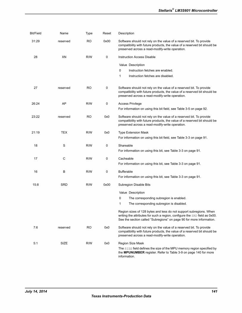
DescriptionResetTypeNameBit/Field
Software should not rely on the value of a reserved bit. To providecompatibility with future products, the value of a reserved bit should bepreserved across a read-modify-write operation.
0x00ROreserved31:29
Instruction Access Disable
DescriptionValue
Instruction fetches are enabled.0
Instruction fetches are disabled.1
0R/WXN28
Software should not rely on the value of a reserved bit. To providecompatibility with future products, the value of a reserved bit should bepreserved across a read-modify-write operation.
0ROreserved27
Access PrivilegeFor information on using this bit field, see Table 3-5 on page 92.
0R/WAP26:24
Software should not rely on the value of a reserved bit. To providecompatibility with future products, the value of a reserved bit should bepreserved across a read-modify-write operation.
0x0ROreserved23:22
Type Extension MaskFor information on using this bit field, see Table 3-3 on page 91.
0x0R/WTEX21:19
ShareableFor information on using this bit, see Table 3-3 on page 91.
0R/WS18
CacheableFor information on using this bit, see Table 3-3 on page 91.
0R/WC17
BufferableFor information on using this bit, see Table 3-3 on page 91.
0R/WB16
Subregion Disable Bits
DescriptionValue
The corresponding subregion is enabled.0
The corresponding subregion is disabled.1
Region sizes of 128 bytes and less do not support subregions. Whenwriting the attributes for such a region, configure the SRD field as 0x00.See the section called “Subregions” on page 90 for more information.
0x00R/WSRD15:8
Software should not rely on the value of a reserved bit. To providecompatibility with future products, the value of a reserved bit should bepreserved across a read-modify-write operation.
0x0ROreserved7:6
Region Size MaskThe SIZE field defines the size of the MPU memory region specified bythe MPUNUMBER register. Refer to Table 3-9 on page 140 for moreinformation.
0x0R/WSIZE5:1
141July 14, 2014Texas Instruments-Production Data
Stellaris® LM3S601 Microcontroller

DescriptionResetTypeNameBit/Field
Region Enable
DescriptionValue
The region is disabled.0
The region is enabled.1
0R/WENABLE0
July 14, 2014142Texas Instruments-Production Data
Cortex-M3 Peripherals
4 JTAG InterfaceThe Joint Test Action Group (JTAG) port is an IEEE standard that defines a Test Access Port andBoundary Scan Architecture for digital integrated circuits and provides a standardized serial interfacefor controlling the associated test logic. The TAP, Instruction Register (IR), and Data Registers (DR)can be used to test the interconnections of assembled printed circuit boards and obtain manufacturinginformation on the components. The JTAG Port also provides a means of accessing and controllingdesign-for-test features such as I/O pin observation and control, scan testing, and debugging.
The JTAG port is comprised of five pins: TRST, TCK, TMS, TDI, and TDO. Data is transmitted seriallyinto the controller on TDI and out of the controller on TDO. The interpretation of this data is dependenton the current state of the TAP controller. For detailed information on the operation of the JTAGport and TAP controller, please refer to the IEEE Standard 1149.1-Test Access Port andBoundary-Scan Architecture.
The Stellaris® JTAG controller works with the ARM JTAG controller built into the Cortex-M3 core.This is implemented by multiplexing the TDO outputs from both JTAG controllers. ARM JTAGinstructions select the ARM TDO output while Stellaris JTAG instructions select the Stellaris TDOoutputs. The multiplexer is controlled by the Stellaris JTAG controller, which has comprehensiveprogramming for the ARM, Stellaris, and unimplemented JTAG instructions.
The Stellaris JTAG module has the following features:
IEEE 1149.1-1990 compatible Test Access Port (TAP) controller
Four-bit Instruction Register (IR) chain for storing JTAG instructions
IEEE standard instructions: BYPASS, IDCODE, SAMPLE/PRELOAD, EXTEST and INTEST
ARM additional instructions: APACC, DPACC and ABORT
Integrated ARM Serial Wire Debug (SWD)
See the ARM® Debug Interface V5 Architecture Specification for more information on the ARMJTAG controller.
143July 14, 2014Texas Instruments-Production Data
Stellaris® LM3S601 Microcontroller
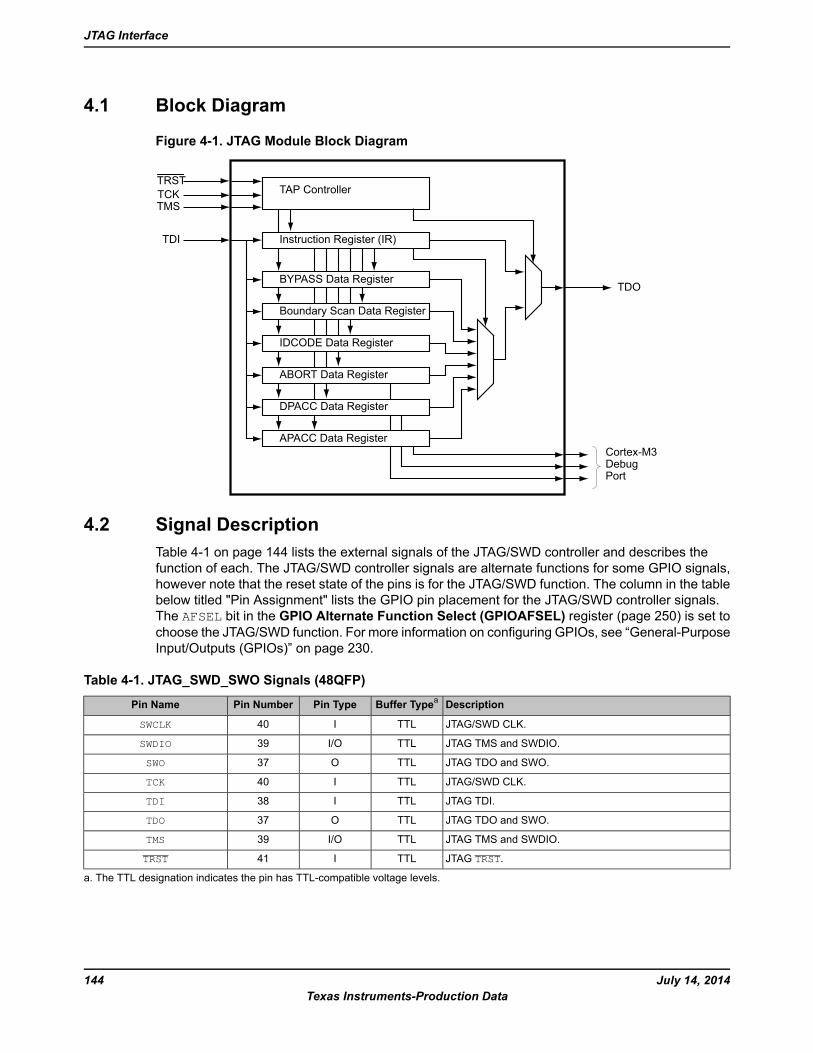
4.1 Block Diagram
Figure 4-1. JTAG Module Block Diagram
Instruction Register (IR)
TAP Controller
BYPASS Data Register
Boundary Scan Data Register
IDCODE Data Register
ABORT Data Register
DPACC Data Register
APACC Data Register
TCKTMS
TDI
TDO
Cortex-M3DebugPort
TRST
4.2 Signal DescriptionTable 4-1 on page 144 lists the external signals of the JTAG/SWD controller and describes thefunction of each. The JTAG/SWD controller signals are alternate functions for some GPIO signals,however note that the reset state of the pins is for the JTAG/SWD function. The column in the tablebelow titled "Pin Assignment" lists the GPIO pin placement for the JTAG/SWD controller signals.The AFSEL bit in the GPIO Alternate Function Select (GPIOAFSEL) register (page 250) is set tochoose the JTAG/SWD function. For more information on configuring GPIOs, see “General-PurposeInput/Outputs (GPIOs)” on page 230.
Table 4-1. JTAG_SWD_SWO Signals (48QFP)
DescriptionBuffer TypeaPin TypePin NumberPin Name
JTAG/SWD CLK.TTLI40SWCLK
JTAG TMS and SWDIO.TTLI/O39SWDIO
JTAG TDO and SWO.TTLO37SWO
JTAG/SWD CLK.TTLI40TCK
JTAG TDI.TTLI38TDI
JTAG TDO and SWO.TTLO37TDO
JTAG TMS and SWDIO.TTLI/O39TMS
JTAG TRST.TTLI41TRST
a. The TTL designation indicates the pin has TTL-compatible voltage levels.
July 14, 2014144Texas Instruments-Production Data
JTAG Interface
4.3 Functional DescriptionA high-level conceptual drawing of the JTAGmodule is shown in Figure 4-1 on page 144. The JTAGmodule is composed of the Test Access Port (TAP) controller and serial shift chains with parallelupdate registers. The TAP controller is a simple state machine controlled by the TRST, TCK andTMS inputs. The current state of the TAP controller depends on the current value of TRST and thesequence of values captured on TMS at the rising edge of TCK. The TAP controller determines whenthe serial shift chains capture new data, shift data from TDI towards TDO, and update the parallelload registers. The current state of the TAP controller also determines whether the InstructionRegister (IR) chain or one of the Data Register (DR) chains is being accessed.
The serial shift chains with parallel load registers are comprised of a single Instruction Register (IR)chain and multiple Data Register (DR) chains. The current instruction loaded in the parallel loadregister determines which DR chain is captured, shifted, or updated during the sequencing of theTAP controller.
Some instructions, like EXTEST and INTEST, operate on data currently in a DR chain and do notcapture, shift, or update any of the chains. Instructions that are not implemented decode to theBYPASS instruction to ensure that the serial path between TDI and TDO is always connected (seeTable 4-3 on page 149 for a list of implemented instructions).
See “JTAG and Boundary Scan” on page 529 for JTAG timing diagrams.
4.3.1 JTAG Interface PinsThe JTAG interface consists of five standard pins: TRST,TCK, TMS, TDI, and TDO. These pins andtheir associated reset state are given in Table 4-2 on page 145. Detailed information on each pinfollows.
Table 4-2. JTAG Port Pins Reset State
Drive ValueDrive StrengthInternal Pull-DownInternal Pull-UpData DirectionPin Name
N/AN/ADisabledEnabledInputTRST
N/AN/ADisabledEnabledInputTCK
N/AN/ADisabledEnabledInputTMS
N/AN/ADisabledEnabledInputTDI
High-Z2-mA driverDisabledEnabledOutputTDO
4.3.1.1 Test Reset Input (TRST)The TRST pin is an asynchronous active Low input signal for initializing and resetting the JTAG TAPcontroller and associated JTAG circuitry. When TRST is asserted, the TAP controller resets to theTest-Logic-Reset state and remains there while TRST is asserted. When the TAP controller entersthe Test-Logic-Reset state, the JTAG Instruction Register (IR) resets to the default instruction,IDCODE.
By default, the internal pull-up resistor on the TRST pin is enabled after reset. Changes to the pull-upresistor settings on GPIO Port B should ensure that the internal pull-up resistor remains enabledon PB7/TRST; otherwise JTAG communication could be lost.
4.3.1.2 Test Clock Input (TCK)The TCK pin is the clock for the JTAG module. This clock is provided so the test logic can operateindependently of any other system clocks. In addition, it ensures that multiple JTAG TAP controllersthat are daisy-chained together can synchronously communicate serial test data between
145July 14, 2014Texas Instruments-Production Data
Stellaris® LM3S601 Microcontroller
components. During normal operation, TCK is driven by a free-running clock with a nominal 50%duty cycle. When necessary, TCK can be stopped at 0 or 1 for extended periods of time. While TCKis stopped at 0 or 1, the state of the TAP controller does not change and data in the JTAG Instructionand Data Registers is not lost.
By default, the internal pull-up resistor on the TCK pin is enabled after reset. This assures that noclocking occurs if the pin is not driven from an external source. The internal pull-up and pull-downresistors can be turned off to save internal power as long as the TCK pin is constantly being drivenby an external source.
4.3.1.3 Test Mode Select (TMS)The TMS pin selects the next state of the JTAG TAP controller. TMS is sampled on the rising edgeof TCK. Depending on the current TAP state and the sampled value of TMS, the next state is entered.Because the TMS pin is sampled on the rising edge of TCK, the IEEE Standard 1149.1 expects thevalue on TMS to change on the falling edge of TCK.
Holding TMS high for five consecutive TCK cycles drives the TAP controller state machine to theTest-Logic-Reset state. When the TAP controller enters the Test-Logic-Reset state, the JTAGInstruction Register (IR) resets to the default instruction, IDCODE. Therefore, this sequence canbe used as a reset mechanism, similar to asserting TRST. The JTAG Test Access Port state machinecan be seen in its entirety in Figure 4-2 on page 147.
By default, the internal pull-up resistor on the TMS pin is enabled after reset. Changes to the pull-upresistor settings on GPIO Port C should ensure that the internal pull-up resistor remains enabledon PC1/TMS; otherwise JTAG communication could be lost.
4.3.1.4 Test Data Input (TDI)The TDI pin provides a stream of serial information to the IR chain and the DR chains. TDI issampled on the rising edge of TCK and, depending on the current TAP state and the currentinstruction, presents this data to the proper shift register chain. Because the TDI pin is sampled onthe rising edge of TCK, the IEEE Standard 1149.1 expects the value on TDI to change on the fallingedge of TCK.
By default, the internal pull-up resistor on the TDI pin is enabled after reset. Changes to the pull-upresistor settings on GPIO Port C should ensure that the internal pull-up resistor remains enabledon PC2/TDI; otherwise JTAG communication could be lost.
4.3.1.5 Test Data Output (TDO)The TDO pin provides an output stream of serial information from the IR chain or the DR chains.The value of TDO depends on the current TAP state, the current instruction, and the data in thechain being accessed. In order to save power when the JTAG port is not being used, the TDO pinis placed in an inactive drive state when not actively shifting out data. Because TDO can be connectedto the TDI of another controller in a daisy-chain configuration, the IEEE Standard 1149.1 expectsthe value on TDO to change on the falling edge of TCK.
By default, the internal pull-up resistor on the TDO pin is enabled after reset. This assures that thepin remains at a constant logic level when the JTAG port is not being used. The internal pull-up andpull-down resistors can be turned off to save internal power if a High-Z output value is acceptableduring certain TAP controller states.
4.3.2 JTAG TAP ControllerThe JTAG TAP controller state machine is shown in Figure 4-2 on page 147. The TAP controllerstate machine is reset to the Test-Logic-Reset state on the assertion of a Power-On-Reset (POR)
July 14, 2014146Texas Instruments-Production Data
JTAG Interface
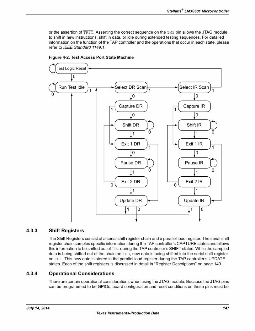
or the assertion of TRST. Asserting the correct sequence on the TMS pin allows the JTAG moduleto shift in new instructions, shift in data, or idle during extended testing sequences. For detailedinformation on the function of the TAP controller and the operations that occur in each state, pleaserefer to IEEE Standard 1149.1.
Figure 4-2. Test Access Port State Machine
Test Logic Reset
Run Test Idle Select DR Scan Select IR Scan
Capture DR Capture IR
Shift DR Shift IR
Exit 1 DR Exit 1 IR
Exit 2 DR Exit 2 IR
Pause DR Pause IR
Update DR Update IR
1 11
1 1
1
1 1
1 1
1 1
1 1
1 10 0
00
00
0 0
0 0
0 0
00
0
0
4.3.3 Shift RegistersThe Shift Registers consist of a serial shift register chain and a parallel load register. The serial shiftregister chain samples specific information during the TAP controller’s CAPTURE states and allowsthis information to be shifted out of TDO during the TAP controller’s SHIFT states. While the sampleddata is being shifted out of the chain on TDO, new data is being shifted into the serial shift registeron TDI. This new data is stored in the parallel load register during the TAP controller’s UPDATEstates. Each of the shift registers is discussed in detail in “Register Descriptions” on page 149.
4.3.4 Operational ConsiderationsThere are certain operational considerations when using the JTAGmodule. Because the JTAG pinscan be programmed to be GPIOs, board configuration and reset conditions on these pins must be
147July 14, 2014Texas Instruments-Production Data
Stellaris® LM3S601 Microcontroller
considered. In addition, because the JTAG module has integrated ARM Serial Wire Debug, themethod for switching between these two operational modes is described below.
4.3.4.1 GPIO FunctionalityWhen the microcontroller is reset with either a POR or RST, the JTAG port pins default to their JTAGconfigurations. The default configuration includes enabling the pull-up resistors (setting GPIOPURto 1 for PB7 and PC[3:0]) and enabling the alternate hardware function (setting GPIOAFSEL to1 for PB7 and PC[3:0]) on the JTAG pins.
It is possible for software to configure these pins as GPIOs after reset by writing 0s to PB7 andPC[3:0] in the GPIOAFSEL register. If the user does not require the JTAG port for debugging orboard-level testing, this provides five more GPIOs for use in the design.
Caution – If the JTAGpins are used asGPIOs in a design, PB7 and PC2 cannot have external pull-downresistors connected to both of them at the same time. If both pins are pulled Low during reset, thecontroller has unpredictable behavior. If this happens, remove one or both of the pull-down resistors,and apply RST or power-cycle the part.
It is possible to create a software sequence that prevents the debugger from connecting to the Stellarismicrocontroller. If the program code loaded into flash immediately changes the JTAG pins to theirGPIO functionality, the debugger may not have enough time to connect and halt the controller beforethe JTAG pin functionality switches. This may lock the debugger out of the part. This can be avoidedwith a software routine that restores JTAG functionality based on an external or software trigger.
4.3.4.2 Communication with JTAG/SWDBecause the debug clock and the system clock can be running at different frequencies, care mustbe taken to maintain reliable communication with the JTAG/SWD interface. In the Capture-DR state,the result of the previous transaction, if any, is returned, together with a 3-bit ACK response. Softwareshould check the ACK response to see if the previous operation has completed before initiating anew transaction. Alternatively, if the system clock is at least 8 times faster than the debug clock(TCK or SWCLK), the previous operation has enough time to complete and the ACK bits do not haveto be checked.
4.3.4.3 ARM Serial Wire Debug (SWD)In order to seamlessly integrate the ARM Serial Wire Debug (SWD) functionality, a serial-wiredebugger must be able to connect to the Cortex-M3 core without having to perform, or have anyknowledge of, JTAG cycles. This is accomplished with a SWD preamble that is issued before theSWD session begins.
The switching preamble used to enable the SWD interface of the SWJ-DP module starts with theTAP controller in the Test-Logic-Reset state. From here, the preamble sequences the TAP controllerthrough the following states: Run Test Idle, Select DR, Select IR, Capture IR, Exit1 IR, Update IR,Run Test Idle, Select DR, Select IR, Capture IR, Exit1 IR, Update IR, Run Test Idle, Select DR,Select IR, and Test-Logic-Reset states.
Stepping through the JTAG TAP Instruction Register (IR) load sequences of the TAP state machinetwice without shifting in a new instruction enables the SWD interface and disables the JTAG interface.For more information on this operation and the SWD interface, see the ARM® Debug Interface V5Architecture Specification.
Because this sequence is a valid series of JTAG operations that could be issued, the ARM JTAGTAP controller is not fully compliant to the IEEE Standard 1149.1. This is the only instance wherethe ARM JTAG TAP controller does not meet full compliance with the specification. Due to the low
July 14, 2014148Texas Instruments-Production Data
JTAG Interface
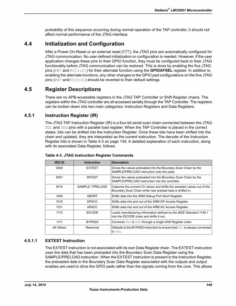
probability of this sequence occurring during normal operation of the TAP controller, it should notaffect normal performance of the JTAG interface.
4.4 Initialization and ConfigurationAfter a Power-On-Reset or an external reset (RST), the JTAG pins are automatically configured forJTAG communication. No user-defined initialization or configuration is needed. However, if the userapplication changes these pins to their GPIO function, they must be configured back to their JTAGfunctionality before JTAG communication can be restored. This is done by enabling the five JTAGpins (PB7 and PC[3:0]) for their alternate function using the GPIOAFSEL register. In addition toenabling the alternate functions, any other changes to the GPIO pad configurations on the five JTAGpins (PB7 andPC[3:0]) should be reverted to their default settings.
4.5 Register DescriptionsThere are no APB-accessible registers in the JTAG TAP Controller or Shift Register chains. Theregisters within the JTAG controller are all accessed serially through the TAP Controller. The registerscan be broken down into two main categories: Instruction Registers and Data Registers.
4.5.1 Instruction Register (IR)The JTAG TAP Instruction Register (IR) is a four-bit serial scan chain connected between the JTAGTDI and TDO pins with a parallel load register. When the TAP Controller is placed in the correctstates, bits can be shifted into the Instruction Register. Once these bits have been shifted into thechain and updated, they are interpreted as the current instruction. The decode of the InstructionRegister bits is shown in Table 4-3 on page 149. A detailed explanation of each instruction, alongwith its associated Data Register, follows.
Table 4-3. JTAG Instruction Register Commands
DescriptionInstructionIR[3:0]
Drives the values preloaded into the Boundary Scan Chain by theSAMPLE/PRELOAD instruction onto the pads.
EXTEST0000
Drives the values preloaded into the Boundary Scan Chain by theSAMPLE/PRELOAD instruction into the controller.
INTEST0001
Captures the current I/O values and shifts the sampled values out of theBoundary Scan Chain while new preload data is shifted in.
SAMPLE / PRELOAD0010
Shifts data into the ARM Debug Port Abort Register.ABORT1000
Shifts data into and out of the ARM DP Access Register.DPACC1010
Shifts data into and out of the ARM AC Access Register.APACC1011
Loads manufacturing information defined by the IEEE Standard 1149.1into the IDCODE chain and shifts it out.
IDCODE1110
Connects TDI to TDO through a single Shift Register chain.BYPASS1111
Defaults to the BYPASS instruction to ensure that TDI is always connectedto TDO.
ReservedAll Others
4.5.1.1 EXTEST InstructionThe EXTEST instruction is not associated with its own Data Register chain. The EXTEST instructionuses the data that has been preloaded into the Boundary Scan Data Register using theSAMPLE/PRELOAD instruction. When the EXTEST instruction is present in the Instruction Register,the preloaded data in the Boundary Scan Data Register associated with the outputs and outputenables are used to drive the GPIO pads rather than the signals coming from the core. This allows
149July 14, 2014Texas Instruments-Production Data
Stellaris® LM3S601 Microcontroller
tests to be developed that drive known values out of the controller, which can be used to verifyconnectivity. While the EXTEST instruction is present in the Instruction Register, the Boundary ScanData Register can be accessed to sample and shift out the current data and load new data into theBoundary Scan Data Register.
4.5.1.2 INTEST InstructionThe INTEST instruction is not associated with its own Data Register chain. The INTEST instructionuses the data that has been preloaded into the Boundary Scan Data Register using theSAMPLE/PRELOAD instruction. When the INTEST instruction is present in the Instruction Register,the preloaded data in the Boundary Scan Data Register associated with the inputs are used to drivethe signals going into the core rather than the signals coming from the GPIO pads. This allows teststo be developed that drive known values into the controller, which can be used for testing. It isimportant to note that although the RST input pin is on the Boundary Scan Data Register chain, itis only observable. While the INTEXT instruction is present in the Instruction Register, the BoundaryScan Data Register can be accessed to sample and shift out the current data and load new datainto the Boundary Scan Data Register.
4.5.1.3 SAMPLE/PRELOAD InstructionThe SAMPLE/PRELOAD instruction connects the Boundary Scan Data Register chain betweenTDI and TDO. This instruction samples the current state of the pad pins for observation and preloadsnew test data. Each GPIO pad has an associated input, output, and output enable signal. When theTAP controller enters the Capture DR state during this instruction, the input, output, and output-enablesignals to each of the GPIO pads are captured. These samples are serially shifted out of TDO whilethe TAP controller is in the Shift DR state and can be used for observation or comparison in varioustests.
While these samples of the inputs, outputs, and output enables are being shifted out of the BoundaryScan Data Register, new data is being shifted into the Boundary Scan Data Register from TDI.Once the new data has been shifted into the Boundary Scan Data Register, the data is saved in theparallel load registers when the TAP controller enters the Update DR state. This update of theparallel load register preloads data into the Boundary Scan Data Register that is associated witheach input, output, and output enable. This preloaded data can be used with the EXTEST andINTEST instructions to drive data into or out of the controller. Please see “Boundary Scan DataRegister” on page 152 for more information.
4.5.1.4 ABORT InstructionThe ABORT instruction connects the associated ABORT Data Register chain between TDI andTDO. This instruction provides read and write access to the ABORT Register of the ARM DebugAccess Port (DAP). Shifting the proper data into this Data Register clears various error bits or initiatesa DAP abort of a previous request. Please see the “ABORT Data Register” on page 152 for moreinformation.
4.5.1.5 DPACC InstructionThe DPACC instruction connects the associated DPACC Data Register chain between TDI andTDO. This instruction provides read and write access to the DPACC Register of the ARM DebugAccess Port (DAP). Shifting the proper data into this register and reading the data output from thisregister allows read and write access to the ARM debug and status registers. Please see “DPACCData Register” on page 152 for more information.
July 14, 2014150Texas Instruments-Production Data
JTAG Interface
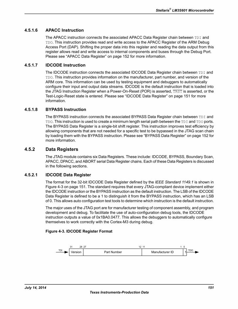
4.5.1.6 APACC InstructionThe APACC instruction connects the associated APACC Data Register chain between TDI andTDO. This instruction provides read and write access to the APACC Register of the ARM DebugAccess Port (DAP). Shifting the proper data into this register and reading the data output from thisregister allows read and write access to internal components and buses through the Debug Port.Please see “APACC Data Register” on page 152 for more information.
4.5.1.7 IDCODE InstructionThe IDCODE instruction connects the associated IDCODE Data Register chain between TDI andTDO. This instruction provides information on the manufacturer, part number, and version of theARM core. This information can be used by testing equipment and debuggers to automaticallyconfigure their input and output data streams. IDCODE is the default instruction that is loaded intothe JTAG Instruction Register when a Power-On-Reset (POR) is asserted, TRST is asserted, or theTest-Logic-Reset state is entered. Please see “IDCODE Data Register” on page 151 for moreinformation.
4.5.1.8 BYPASS InstructionThe BYPASS instruction connects the associated BYPASS Data Register chain between TDI andTDO. This instruction is used to create a minimum length serial path between the TDI and TDO ports.The BYPASS Data Register is a single-bit shift register. This instruction improves test efficiency byallowing components that are not needed for a specific test to be bypassed in the JTAG scan chainby loading them with the BYPASS instruction. Please see “BYPASS Data Register” on page 152 formore information.
4.5.2 Data RegistersThe JTAGmodule contains six Data Registers. These include: IDCODE, BYPASS, Boundary Scan,APACC, DPACC, and ABORT serial Data Register chains. Each of these Data Registers is discussedin the following sections.
4.5.2.1 IDCODE Data RegisterThe format for the 32-bit IDCODE Data Register defined by the IEEE Standard 1149.1 is shown inFigure 4-3 on page 151. The standard requires that every JTAG-compliant device implement eitherthe IDCODE instruction or the BYPASS instruction as the default instruction. The LSB of the IDCODEData Register is defined to be a 1 to distinguish it from the BYPASS instruction, which has an LSBof 0. This allows auto configuration test tools to determine which instruction is the default instruction.
The major uses of the JTAG port are for manufacturer testing of component assembly, and programdevelopment and debug. To facilitate the use of auto-configuration debug tools, the IDCODEinstruction outputs a value of 0x1BA0.0477. This allows the debuggers to automatically configurethemselves to work correctly with the Cortex-M3 during debug.
Figure 4-3. IDCODE Register Format
Version Part Number Manufacturer ID 1
31 28 27 12 11 1 0TDOTDI
151July 14, 2014Texas Instruments-Production Data
Stellaris® LM3S601 Microcontroller
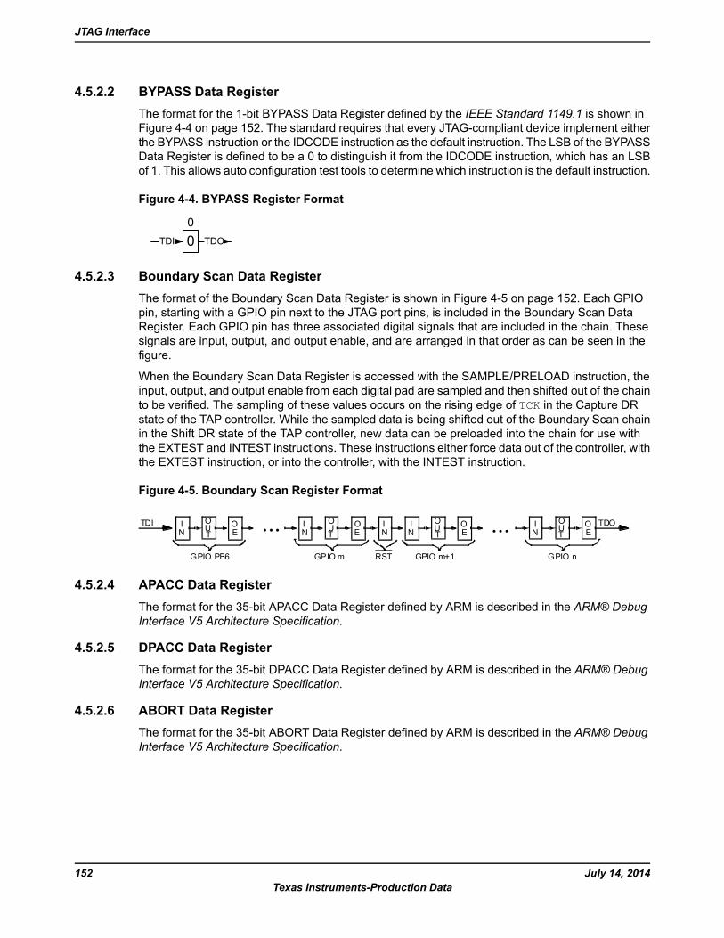
4.5.2.2 BYPASS Data RegisterThe format for the 1-bit BYPASS Data Register defined by the IEEE Standard 1149.1 is shown inFigure 4-4 on page 152. The standard requires that every JTAG-compliant device implement eitherthe BYPASS instruction or the IDCODE instruction as the default instruction. The LSB of the BYPASSData Register is defined to be a 0 to distinguish it from the IDCODE instruction, which has an LSBof 1. This allows auto configuration test tools to determine which instruction is the default instruction.
Figure 4-4. BYPASS Register Format
0 TDOTDI
0
4.5.2.3 Boundary Scan Data RegisterThe format of the Boundary Scan Data Register is shown in Figure 4-5 on page 152. Each GPIOpin, starting with a GPIO pin next to the JTAG port pins, is included in the Boundary Scan DataRegister. Each GPIO pin has three associated digital signals that are included in the chain. Thesesignals are input, output, and output enable, and are arranged in that order as can be seen in thefigure.
When the Boundary Scan Data Register is accessed with the SAMPLE/PRELOAD instruction, theinput, output, and output enable from each digital pad are sampled and then shifted out of the chainto be verified. The sampling of these values occurs on the rising edge of TCK in the Capture DRstate of the TAP controller. While the sampled data is being shifted out of the Boundary Scan chainin the Shift DR state of the TAP controller, new data can be preloaded into the chain for use withthe EXTEST and INTEST instructions. These instructions either force data out of the controller, withthe EXTEST instruction, or into the controller, with the INTEST instruction.
Figure 4-5. Boundary Scan Register Format
O TDOTDI OIN EU
TOOI
N EUT
OOIN EU
TOOI
N EUT
IN... ...
RSTGPIO PB6 GPIO m GPIO m+1 GPIO n
4.5.2.4 APACC Data RegisterThe format for the 35-bit APACC Data Register defined by ARM is described in the ARM® DebugInterface V5 Architecture Specification.
4.5.2.5 DPACC Data RegisterThe format for the 35-bit DPACC Data Register defined by ARM is described in the ARM® DebugInterface V5 Architecture Specification.
4.5.2.6 ABORT Data RegisterThe format for the 35-bit ABORT Data Register defined by ARM is described in the ARM® DebugInterface V5 Architecture Specification.
July 14, 2014152Texas Instruments-Production Data
JTAG Interface
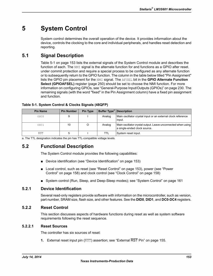
5 System ControlSystem control determines the overall operation of the device. It provides information about thedevice, controls the clocking to the core and individual peripherals, and handles reset detection andreporting.
5.1 Signal DescriptionTable 5-1 on page 153 lists the external signals of the System Control module and describes thefunction of each. The NMI signal is the alternate function for and functions as a GPIO after reset.under commit protection and require a special process to be configured as any alternate functionor to subsequently return to the GPIO function. The column in the table below titled "Pin Assignment"lists the GPIO pin placement for the NMI signal. The AFSEL bit in the GPIO Alternate FunctionSelect (GPIOAFSEL) register (page 250) should be set to choose the NMI function. For moreinformation on configuring GPIOs, see “General-Purpose Input/Outputs (GPIOs)” on page 230. Theremaining signals (with the word "fixed" in the Pin Assignment column) have a fixed pin assignmentand function.
Table 5-1. System Control & Clocks Signals (48QFP)
DescriptionBuffer TypeaPin TypePin NumberPin Name
Main oscillator crystal input or an external clock referenceinput.
AnalogI9OSC0
Main oscillator crystal output. Leave unconnected when usinga single-ended clock source.
AnalogO10OSC1
System reset input.TTLI5RST
a. The TTL designation indicates the pin has TTL-compatible voltage levels.
5.2 Functional DescriptionThe System Control module provides the following capabilities:
Device identification (see “Device Identification” on page 153)
Local control, such as reset (see “Reset Control” on page 153), power (see “PowerControl” on page 158) and clock control (see “Clock Control” on page 158)
System control (Run, Sleep, and Deep-Sleep modes); see “System Control” on page 161
5.2.1 Device IdentificationSeveral read-only registers provide software with information on the microcontroller, such as version,part number, SRAM size, flash size, and other features. See theDID0,DID1, andDC0-DC4 registers.
5.2.2 Reset ControlThis section discusses aspects of hardware functions during reset as well as system softwarerequirements following the reset sequence.
5.2.2.1 Reset SourcesThe controller has six sources of reset:
1. External reset input pin (RST) assertion; see “External RST Pin” on page 155.
153July 14, 2014Texas Instruments-Production Data
Stellaris® LM3S601 Microcontroller
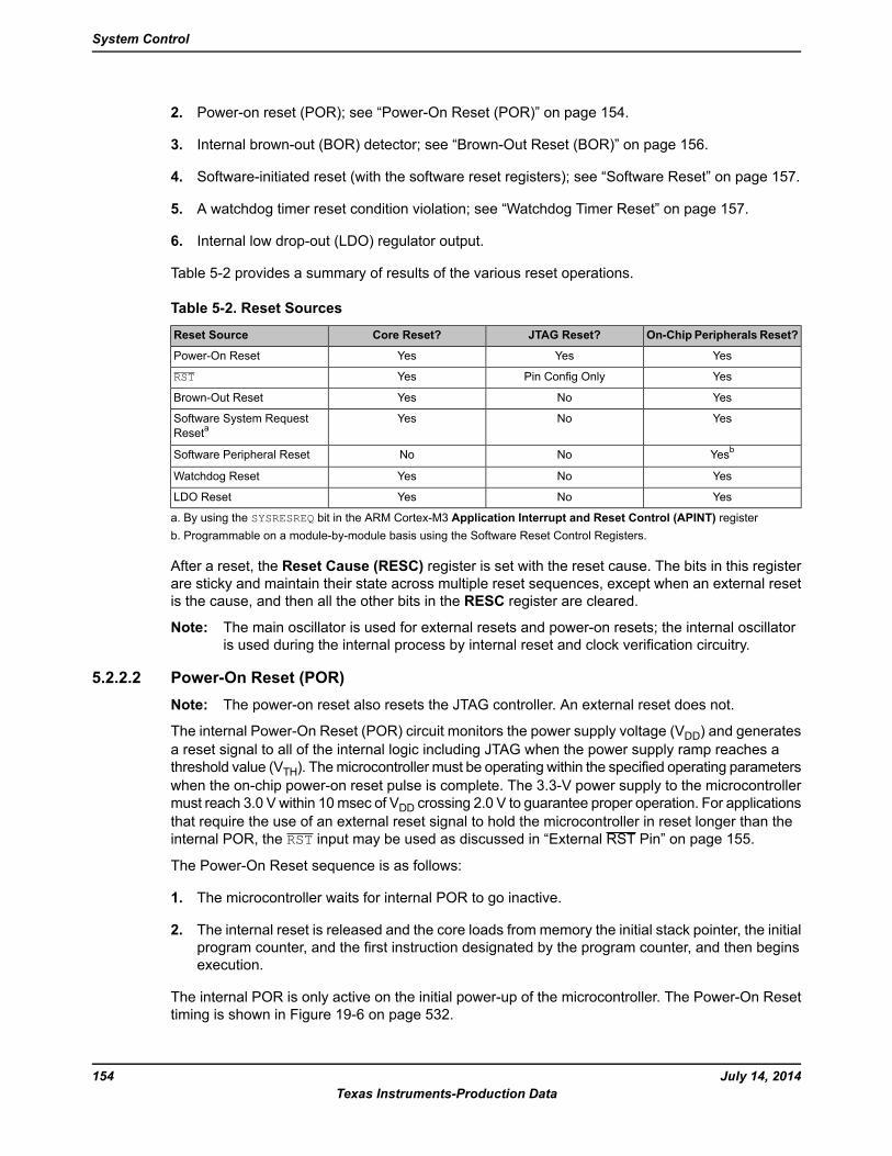
2. Power-on reset (POR); see “Power-On Reset (POR)” on page 154.
3. Internal brown-out (BOR) detector; see “Brown-Out Reset (BOR)” on page 156.
4. Software-initiated reset (with the software reset registers); see “Software Reset” on page 157.
5. A watchdog timer reset condition violation; see “Watchdog Timer Reset” on page 157.
6. Internal low drop-out (LDO) regulator output.
Table 5-2 provides a summary of results of the various reset operations.
Table 5-2. Reset Sources
On-Chip Peripherals Reset?JTAG Reset?Core Reset?Reset Source
YesYesYesPower-On Reset
YesPin Config OnlyYesRST
YesNoYesBrown-Out Reset
YesNoYesSoftware System RequestReseta
YesbNoNoSoftware Peripheral Reset
YesNoYesWatchdog Reset
YesNoYesLDO Reset
a. By using the SYSRESREQ bit in the ARM Cortex-M3 Application Interrupt and Reset Control (APINT) registerb. Programmable on a module-by-module basis using the Software Reset Control Registers.
After a reset, the Reset Cause (RESC) register is set with the reset cause. The bits in this registerare sticky and maintain their state across multiple reset sequences, except when an external resetis the cause, and then all the other bits in the RESC register are cleared.
Note: The main oscillator is used for external resets and power-on resets; the internal oscillatoris used during the internal process by internal reset and clock verification circuitry.
5.2.2.2 Power-On Reset (POR)Note: The power-on reset also resets the JTAG controller. An external reset does not.
The internal Power-On Reset (POR) circuit monitors the power supply voltage (VDD) and generatesa reset signal to all of the internal logic including JTAG when the power supply ramp reaches athreshold value (VTH). Themicrocontroller must be operating within the specified operating parameterswhen the on-chip power-on reset pulse is complete. The 3.3-V power supply to the microcontrollermust reach 3.0 V within 10msec of VDD crossing 2.0 V to guarantee proper operation. For applicationsthat require the use of an external reset signal to hold the microcontroller in reset longer than theinternal POR, the RST input may be used as discussed in “External RST Pin” on page 155.
The Power-On Reset sequence is as follows:
1. The microcontroller waits for internal POR to go inactive.
2. The internal reset is released and the core loads from memory the initial stack pointer, the initialprogram counter, and the first instruction designated by the program counter, and then beginsexecution.
The internal POR is only active on the initial power-up of the microcontroller. The Power-On Resettiming is shown in Figure 19-6 on page 532.
July 14, 2014154Texas Instruments-Production Data
System Control
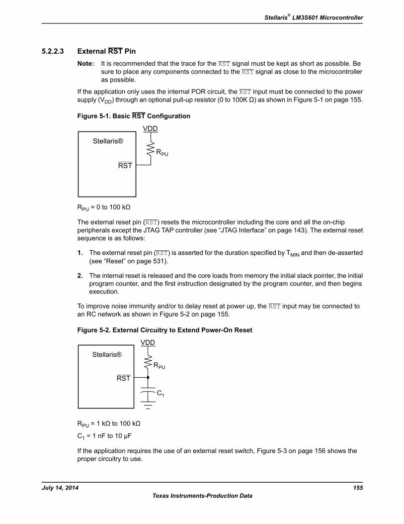
5.2.2.3 External RST PinNote: It is recommended that the trace for the RST signal must be kept as short as possible. Be
sure to place any components connected to the RST signal as close to the microcontrolleras possible.
If the application only uses the internal POR circuit, the RST input must be connected to the powersupply (VDD) through an optional pull-up resistor (0 to 100K Ω) as shown in Figure 5-1 on page 155.
Figure 5-1. Basic RST Configuration
PU
RST
Stellaris®R
VDD
RPU = 0 to 100 kΩ
The external reset pin (RST) resets the microcontroller including the core and all the on-chipperipherals except the JTAG TAP controller (see “JTAG Interface” on page 143). The external resetsequence is as follows:
1. The external reset pin (RST) is asserted for the duration specified by TMIN and then de-asserted(see “Reset” on page 531).
2. The internal reset is released and the core loads from memory the initial stack pointer, the initialprogram counter, and the first instruction designated by the program counter, and then beginsexecution.
To improve noise immunity and/or to delay reset at power up, the RST input may be connected toan RC network as shown in Figure 5-2 on page 155.
Figure 5-2. External Circuitry to Extend Power-On Reset
PU
C1
RST
Stellaris®R
VDD
RPU = 1 kΩ to 100 kΩ
C1 = 1 nF to 10 µF
If the application requires the use of an external reset switch, Figure 5-3 on page 156 shows theproper circuitry to use.
155July 14, 2014Texas Instruments-Production Data
Stellaris® LM3S601 Microcontroller
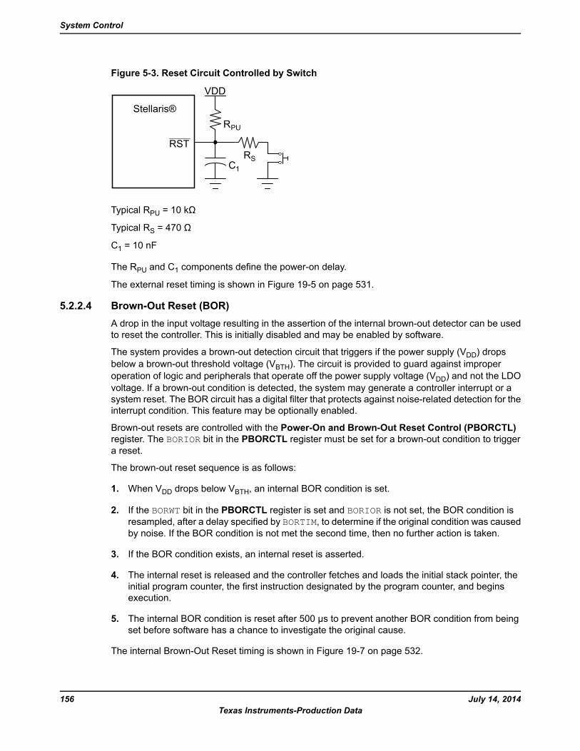
Figure 5-3. Reset Circuit Controlled by Switch
PU
C1
RS
RST
Stellaris®R
VDD
Typical RPU = 10 kΩ
Typical RS = 470 Ω
C1 = 10 nF
The RPU and C1 components define the power-on delay.
The external reset timing is shown in Figure 19-5 on page 531.
5.2.2.4 Brown-Out Reset (BOR)A drop in the input voltage resulting in the assertion of the internal brown-out detector can be usedto reset the controller. This is initially disabled and may be enabled by software.
The system provides a brown-out detection circuit that triggers if the power supply (VDD) dropsbelow a brown-out threshold voltage (VBTH). The circuit is provided to guard against improperoperation of logic and peripherals that operate off the power supply voltage (VDD) and not the LDOvoltage. If a brown-out condition is detected, the system may generate a controller interrupt or asystem reset. The BOR circuit has a digital filter that protects against noise-related detection for theinterrupt condition. This feature may be optionally enabled.
Brown-out resets are controlled with the Power-On and Brown-Out Reset Control (PBORCTL)register. The BORIOR bit in the PBORCTL register must be set for a brown-out condition to triggera reset.
The brown-out reset sequence is as follows:
1. When VDD drops below VBTH, an internal BOR condition is set.
2. If the BORWT bit in the PBORCTL register is set and BORIOR is not set, the BOR condition isresampled, after a delay specified by BORTIM, to determine if the original condition was causedby noise. If the BOR condition is not met the second time, then no further action is taken.
3. If the BOR condition exists, an internal reset is asserted.
4. The internal reset is released and the controller fetches and loads the initial stack pointer, theinitial program counter, the first instruction designated by the program counter, and beginsexecution.
5. The internal BOR condition is reset after 500 µs to prevent another BOR condition from beingset before software has a chance to investigate the original cause.
The internal Brown-Out Reset timing is shown in Figure 19-7 on page 532.
July 14, 2014156Texas Instruments-Production Data
System Control
5.2.2.5 Software ResetSoftware can reset a specific peripheral or generate a reset to the entire system .
Peripherals can be individually reset by software via three registers that control reset signals to eachperipheral (see the SRCRn registers). If the bit position corresponding to a peripheral is set andsubsequently cleared, the peripheral is reset. The encoding of the reset registers is consistent withthe encoding of the clock gating control for peripherals and on-chip functions (see “SystemControl” on page 161). Note that all reset signals for all clocks of the specified unit are asserted asa result of a software-initiated reset.
The entire system can be reset by software by setting the SYSRESETREQ bit in the Cortex-M3Application Interrupt and Reset Control register resets the entire system including the core. Thesoftware-initiated system reset sequence is as follows:
1. A software system reset is initiated by writing the SYSRESETREQ bit in the ARM Cortex-M3Application Interrupt and Reset Control register.
2. An internal reset is asserted.
3. The internal reset is deasserted and the controller loads from memory the initial stack pointer,the initial program counter, and the first instruction designated by the program counter, andthen begins execution.
The software-initiated system reset timing is shown in Figure 19-8 on page 532.
5.2.2.6 Watchdog Timer ResetThe watchdog timer module's function is to prevent system hangs. The watchdog timer can beconfigured to generate an interrupt to the controller on its first time-out, and to generate a resetsignal on its second time-out.
After the first time-out event, the 32-bit counter is reloaded with the value of theWatchdog TimerLoad (WDTLOAD) register, and the timer resumes counting down from that value. If the timer countsdown to its zero state again before the first time-out interrupt is cleared, and the reset signal hasbeen enabled, the watchdog timer asserts its reset signal to the system. The watchdog timer resetsequence is as follows:
1. The watchdog timer times out for the second time without being serviced.
2. An internal reset is asserted.
3. The internal reset is released and the controller loads from memory the initial stack pointer, theinitial program counter, the first instruction designated by the program counter, and beginsexecution.
The watchdog reset timing is shown in Figure 19-9 on page 533.
5.2.2.7 Low Drop-Out (LDO)A reset can be initiated when the internal low drop-out (LDO) regulator output goes unregulated.This is initially disabled and may be enabled by software. LDO is controlled with the LDO PowerControl (LDOPCTL) register. The LDO reset sequence is as follows:
1. LDO goes unregulated and the LDOARST bit in the LDOARST register is set.
2. An internal reset is asserted.
157July 14, 2014Texas Instruments-Production Data
Stellaris® LM3S601 Microcontroller
3. The internal reset is released and the controller fetches and loads the initial stack pointer, theinitial program counter, the first instruction designated by the program counter, and beginsexecution.
The LDO reset timing is shown in Figure 19-10 on page 533.
5.2.3 Power ControlThe Stellaris® microcontroller provides an integrated LDO regulator that is used to provide powerto the majority of the controller's internal logic. For power reduction, the LDO regulator providessoftware a mechanism to adjust the regulated value, in small increments (VSTEP), over the rangeof 2.25 V to 2.75 V (inclusive)—or 2.5 V ± 10%. The adjustment is made by changing the value ofthe VADJ field in the LDO Power Control (LDOPCTL) register.
5.2.4 Clock ControlSystem control determines the control of clocks in this part.
5.2.4.1 Fundamental Clock SourcesThere are multiple clock sources for use in the device:
Internal Oscillator (IOSC). The internal oscillator is an on-chip clock source. It does not requirethe use of any external components. The frequency of the internal oscillator is 12 MHz ± 30%.
Main Oscillator (MOSC). The main oscillator provides a frequency-accurate clock source byone of two means: an external single-ended clock source is connected to the OSC0 input pin, oran external crystal is connected across the OSC0 input and OSC1 output pins. The crystal valueallowed depends on whether the main oscillator is used as the clock reference source to thePLL. If so, the crystal must be one of the supported frequencies between 3.579545 MHz through8.192 MHz (inclusive). If the PLL is not being used, the crystal may be any one of the supportedfrequencies between 1 MHz and 8.192 MHz. The single-ended clock source range is from DCthrough the specified speed of the device. The supported crystals are listed in the XTAL bit fieldin the RCC register (see page 173).
The internal system clock (SysClk), is derived from any of the above sources plus two others: theoutput of the main internal PLL, and the internal oscillator divided by four (3 MHz ± 30%). Thefrequency of the PLL clock reference must be in the range of 3.579545MHz to 8.192 MHz (inclusive).Table 5-3 on page 158 shows how the various clock sources can be used in a system.
Table 5-3. Clock Source Options
Used as SysClk?Drive PLL?Clock Source
BYPASS = 1, OSCSRC = 0x1YesBYPASS = 0, OSCSRC = 0x1YesInternal Oscillator (12 MHz)
BYPASS = 1, OSCSRC = 0x2YesBYPASS = 0, OSCSRC = 0x2YesInternal Oscillator divide by 4 (3MHz)
BYPASS = 1, OSCSRC = 0x0YesBYPASS = 0, OSCSRC = 0x0YesMain Oscillator
5.2.4.2 Clock ConfigurationNearly all of the control for the clocks is provided by the Run-Mode Clock Configuration (RCC)register. This register controls the following clock functionality:
Source of clocks in sleep and deep-sleep modes
July 14, 2014158Texas Instruments-Production Data
System Control
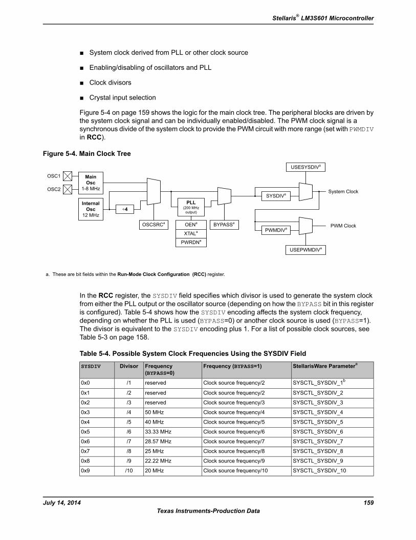
System clock derived from PLL or other clock source
Enabling/disabling of oscillators and PLL
Clock divisors
Crystal input selection
Figure 5-4 on page 159 shows the logic for the main clock tree. The peripheral blocks are driven bythe system clock signal and can be individually enabled/disabled. The PWM clock signal is asynchronous divide of the system clock to provide the PWM circuit with more range (set with PWMDIVin RCC).
Figure 5-4. Main Clock Tree
MainOsc
1-8 MHz
InternalOsc
12 MHz÷4
OSCSRCa
OSC1
OSC2
PLL(200 MHzoutput)
BYPASSa
SYSDIVa
USESYSDIVa
System Clock
PWMDIVa
USEPWMDIVa
PWM ClockOENa
XTALa
PWRDNa
a. These are bit fields within the Run-Mode Clock Configuration (RCC) register.
In the RCC register, the SYSDIV field specifies which divisor is used to generate the system clockfrom either the PLL output or the oscillator source (depending on how the BYPASS bit in this registeris configured). Table 5-4 shows how the SYSDIV encoding affects the system clock frequency,depending on whether the PLL is used (BYPASS=0) or another clock source is used (BYPASS=1).The divisor is equivalent to the SYSDIV encoding plus 1. For a list of possible clock sources, seeTable 5-3 on page 158.
Table 5-4. Possible System Clock Frequencies Using the SYSDIV Field
StellarisWare ParameteraFrequency (BYPASS=1)Frequency(BYPASS=0)
DivisorSYSDIV
SYSCTL_SYSDIV_1bClock source frequency/2reserved/10x0
SYSCTL_SYSDIV_2Clock source frequency/2reserved/20x1
SYSCTL_SYSDIV_3Clock source frequency/3reserved/30x2
SYSCTL_SYSDIV_4Clock source frequency/450 MHz/40x3
SYSCTL_SYSDIV_5Clock source frequency/540 MHz/50x4
SYSCTL_SYSDIV_6Clock source frequency/633.33 MHz/60x5
SYSCTL_SYSDIV_7Clock source frequency/728.57 MHz/70x6
SYSCTL_SYSDIV_8Clock source frequency/825 MHz/80x7
SYSCTL_SYSDIV_9Clock source frequency/922.22 MHz/90x8
SYSCTL_SYSDIV_10Clock source frequency/1020 MHz/100x9
159July 14, 2014Texas Instruments-Production Data
Stellaris® LM3S601 Microcontroller
Table 5-4. Possible System Clock Frequencies Using the SYSDIV Field (continued)
StellarisWare ParameteraFrequency (BYPASS=1)Frequency(BYPASS=0)
DivisorSYSDIV
SYSCTL_SYSDIV_11Clock source frequency/1118.18 MHz/110xA
SYSCTL_SYSDIV_12Clock source frequency/1216.67 MHz/120xB
SYSCTL_SYSDIV_13Clock source frequency/1315.38 MHz/130xC
SYSCTL_SYSDIV_14Clock source frequency/1414.29 MHz/140xD
SYSCTL_SYSDIV_15Clock source frequency/1513.33 MHz/150xE
SYSCTL_SYSDIV_16Clock source frequency/1612.5 MHz (default)/160xF
a. This parameter is used in functions such as SysCtlClockSet() in the Stellaris Peripheral Driver Library.b. SYSCTL_SYSDIV_1 does not set the USESYSDIV bit. As a result, using this parameter without enabling the PLL results
in the system clock having the same frequency as the clock source.
5.2.4.3 Crystal Configuration for the Main Oscillator (MOSC)The main oscillator supports the use of a select number of crystals. If the main oscillator is used bythe PLL as a reference clock, the supported range of crystals is 3.579545 to 8.192 MHz, otherwise,the range of supported crystals is 1 to 8.192 MHz.
The XTAL bit in the RCC register (see page 173) describes the available crystal choices and defaultprogramming values.
Software configures the RCC register XTAL field with the crystal number. If the PLL is used in thedesign, the XTAL field value is internally translated to the PLL settings.
5.2.4.4 Main PLL Frequency ConfigurationThe main PLL is disabled by default during power-on reset and is enabled later by software ifrequired. Software configures the main PLL input reference clock source, specifies the output divisorto set the system clock frequency, and enables the main PLL to drive the output.
If the main oscillator provides the clock reference to the main PLL, the translation provided byhardware and used to program the PLL is available for software in the XTAL to PLL Translation(PLLCFG) register (see page 177). The internal translation provides a translation within ± 1% of thetargeted PLL VCO frequency.
The Crystal Value field (XTAL) in theRun-Mode Clock Configuration (RCC) register (see page 173)describes the available crystal choices and default programming of the PLLCFG register. Any timethe XTAL field changes, the new settings are translated and the internal PLL settings are updated.
5.2.4.5 PLL ModesThe PLL has two modes of operation: Normal and Power-Down
Normal: The PLL multiplies the input clock reference and drives the output.
Power-Down: Most of the PLL internal circuitry is disabled and the PLL does not drive the output.
The modes are programmed using the RCC register fields (see page 173).
5.2.4.6 PLL OperationIf a PLL configuration is changed, the PLL output frequency is unstable until it reconverges (relocks)to the new setting. The time between the configuration change and relock is TREADY (see Table19-7 on page 529). During the relock time, the affected PLL is not usable as a clock reference.
July 14, 2014160Texas Instruments-Production Data
System Control
PLL is changed by one of the following:
Change to the XTAL value in the RCC register—writes of the same value do not cause a relock.
Change in the PLL from Power-Down to Normal mode.
A counter is defined to measure the TREADY requirement. The counter is clocked by the mainoscillator. The range of the main oscillator has been taken into account and the down counter is setto 0x1200 (that is, ~600 μs at an 8.192 MHz external oscillator clock). Hardware is provided to keepthe PLL from being used as a system clock until the TREADY condition is met after one of the twochanges above. It is the user's responsibility to have a stable clock source (like the main oscillator)before the RCC register is switched to use the PLL.
If the main PLL is enabled and the system clock is switched to use the PLL in one step, the systemcontrol hardware continues to clock the controller from the oscillator selected by the RCC registeruntil the main PLL is stable (TREADY time met), after which it changes to the PLL. Software can usemany methods to ensure that the system is clocked from the main PLL, including periodically pollingthe PLLLRIS bit in the Raw Interrupt Status (RIS) register, and enabling the PLL Lock interrupt.
5.2.4.7 Clock Verification TimersThere are three identical clock verification circuits that can be enabled though software. The circuitchecks the faster clock by a slower clock using timers:
The main oscillator checks the PLL.
The main oscillator checks the internal oscillator.
The internal oscillator divided by 64 checks the main oscillator.
If the verification timer function is enabled and a failure is detected, the main clock tree is immediatelyswitched to a working clock and an interrupt is generated to the controller. Software can thendetermine the course of action to take. The actual failure indication and clock switching does notclear without a write to the CLKVCLR register, an external reset, or a POR reset. The clockverification timers are controlled by the PLLVER , IOSCVER , and MOSCVER bits in the RCC register.
5.2.5 System ControlFor power-savings purposes, the RCGCn , SCGCn , and DCGCn registers control the clock gatinglogic for each peripheral or block in the system while the controller is in Run, Sleep, and Deep-Sleepmode, respectively. TheDC1 ,DC2 andDC4 registers act as a write mask for theRCGCn , SCGCn,and DCGCn registers.
There are three levels of operation for the device defined as:
Run Mode. In Run mode, the controller actively executes code. Run mode provides normaloperation of the processor and all of the peripherals that are currently enabled by the RCGCnregisters. The system clock can be any of the available clock sources including the PLL.
Sleep Mode. In Sleep mode, the clock frequency of the active peripherals is unchanged, but theprocessor and the memory subsystem are not clocked and therefore no longer execute code.Sleep mode is entered by the Cortex-M3 core executing a WFI(Wait for Interrupt)instruction. Any properly configured interrupt event in the system will bring the processor backinto Run mode. See “Power Management” on page 80 for more details.
161July 14, 2014Texas Instruments-Production Data
Stellaris® LM3S601 Microcontroller
Peripherals are clocked that are enabled in theSCGCn register when auto-clock gating is enabled(see theRCC register) or theRCGCn register when the auto-clock gating is disabled. The systemclock has the same source and frequency as that during Run mode.
Deep-Sleep Mode. In Deep-Sleep mode, the clock frequency of the active peripherals maychange (depending on the Run mode clock configuration) in addition to the processor clock beingstopped. An interrupt returns the device to Run mode from one of the sleep modes. Deep-Sleepmode is entered by first writing the Deep Sleep Enable bit in the ARM Cortex-M3 NVIC systemcontrol register and then executing a WFI instruction. Any properly configured interrupt event inthe system will bring the processor back into Run mode. See “Power Management” on page 80for more details.
The Cortex-M3 processor core and the memory subsystem are not clocked. Peripherals areclocked that are enabled in theDCGCn register when auto-clock gating is enabled (see theRCCregister) or the RCGCn register when auto-clock gating is disabled. The system clock source isthe main oscillator by default or the internal oscillator specified in the DSLPCLKCFG register ifone is enabled. When the DSLPCLKCFG register is used, the internal oscillator is powered up,if necessary, and the main oscillator is powered down. If the PLL is running at the time of theWFI instruction, hardware will power the PLL down. When the Deep-Sleep exit event occurs,hardware brings the system clock back to the source and frequency it had at the onset ofDeep-Sleep mode before enabling the clocks that had been stopped during the Deep-Sleepduration.
Caution – If the Cortex-M3 Debug Access Port (DAP) has been enabled, and the device wakes from alow power sleep or deep-sleep mode, the core may start executing code before all clocks to peripheralshave been restored to their run mode configuration. The DAP is usually enabled by software toolsaccessing the JTAG or SWD interface when debugging or flash programming. If this condition occurs,a Hard Fault is triggered when software accesses a peripheral with an invalid clock.
A software delay loop can be used at the beginning of the interrupt routine that is used to wake up asystem from aWFI (Wait For Interrupt) instruction. This stalls the execution of any code that accessesa peripheral register that might cause a fault. This loop can be removed for production software as theDAP is most likely not enabled during normal execution.
Because the DAP is disabled by default (power on reset), the user can also power-cycle the device. TheDAP is not enabled unless it is enabled through the JTAG or SWD interface.
5.3 Initialization and ConfigurationThe PLL is configured using direct register writes to the RCC register. The steps required tosuccessfully change the PLL-based system clock are:
1. Bypass the PLL and system clock divider by setting the BYPASS bit and clearing the USESYSbit in the RCC register. This configures the system to run off a “raw” clock source and allowsfor the new PLL configuration to be validated before switching the system clock to the PLL.
2. Select the crystal value (XTAL) and oscillator source (OSCSRC), and clear the PWRDN and OENbits in RCC. Setting the XTAL field automatically pulls valid PLL configuration data for theappropriate crystal, and clearing the PWRDN and OEN bits powers and enables the PLL and itsoutput.
3. Select the desired system divider (SYSDIV) inRCC and set the USESYS bit inRCC. The SYSDIVfield determines the system frequency for the microcontroller.
July 14, 2014162Texas Instruments-Production Data
System Control
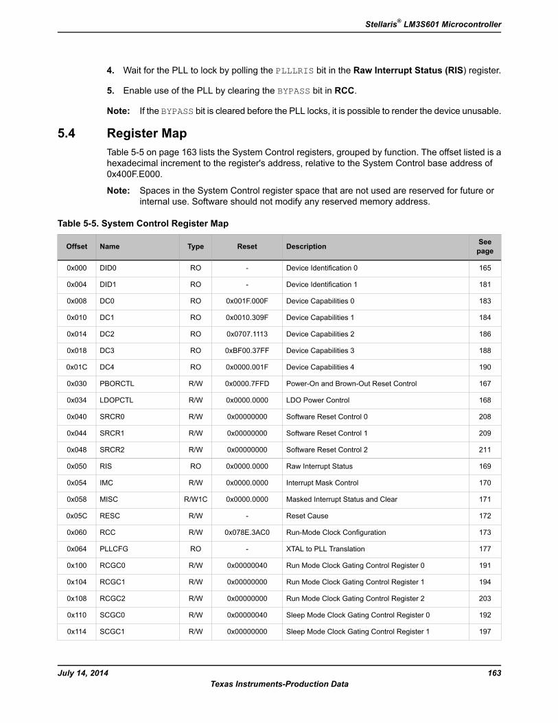
4. Wait for the PLL to lock by polling the PLLLRIS bit in the Raw Interrupt Status (RIS) register.
5. Enable use of the PLL by clearing the BYPASS bit in RCC.
Note: If the BYPASS bit is cleared before the PLL locks, it is possible to render the device unusable.
5.4 Register MapTable 5-5 on page 163 lists the System Control registers, grouped by function. The offset listed is ahexadecimal increment to the register's address, relative to the System Control base address of0x400F.E000.
Note: Spaces in the System Control register space that are not used are reserved for future orinternal use. Software should not modify any reserved memory address.
Table 5-5. System Control Register Map
SeepageDescriptionResetTypeNameOffset
165Device Identification 0-RODID00x000
181Device Identification 1-RODID10x004
183Device Capabilities 00x001F.000FRODC00x008
184Device Capabilities 10x0010.309FRODC10x010
186Device Capabilities 20x0707.1113RODC20x014
188Device Capabilities 30xBF00.37FFRODC30x018
190Device Capabilities 40x0000.001FRODC40x01C
167Power-On and Brown-Out Reset Control0x0000.7FFDR/WPBORCTL0x030
168LDO Power Control0x0000.0000R/WLDOPCTL0x034
208Software Reset Control 00x00000000R/WSRCR00x040
209Software Reset Control 10x00000000R/WSRCR10x044
211Software Reset Control 20x00000000R/WSRCR20x048
169Raw Interrupt Status0x0000.0000RORIS0x050
170Interrupt Mask Control0x0000.0000R/WIMC0x054
171Masked Interrupt Status and Clear0x0000.0000R/W1CMISC0x058
172Reset Cause-R/WRESC0x05C
173Run-Mode Clock Configuration0x078E.3AC0R/WRCC0x060
177XTAL to PLL Translation-ROPLLCFG0x064
191Run Mode Clock Gating Control Register 00x00000040R/WRCGC00x100
194Run Mode Clock Gating Control Register 10x00000000R/WRCGC10x104
203Run Mode Clock Gating Control Register 20x00000000R/WRCGC20x108
192Sleep Mode Clock Gating Control Register 00x00000040R/WSCGC00x110
197Sleep Mode Clock Gating Control Register 10x00000000R/WSCGC10x114
163July 14, 2014Texas Instruments-Production Data
Stellaris® LM3S601 Microcontroller
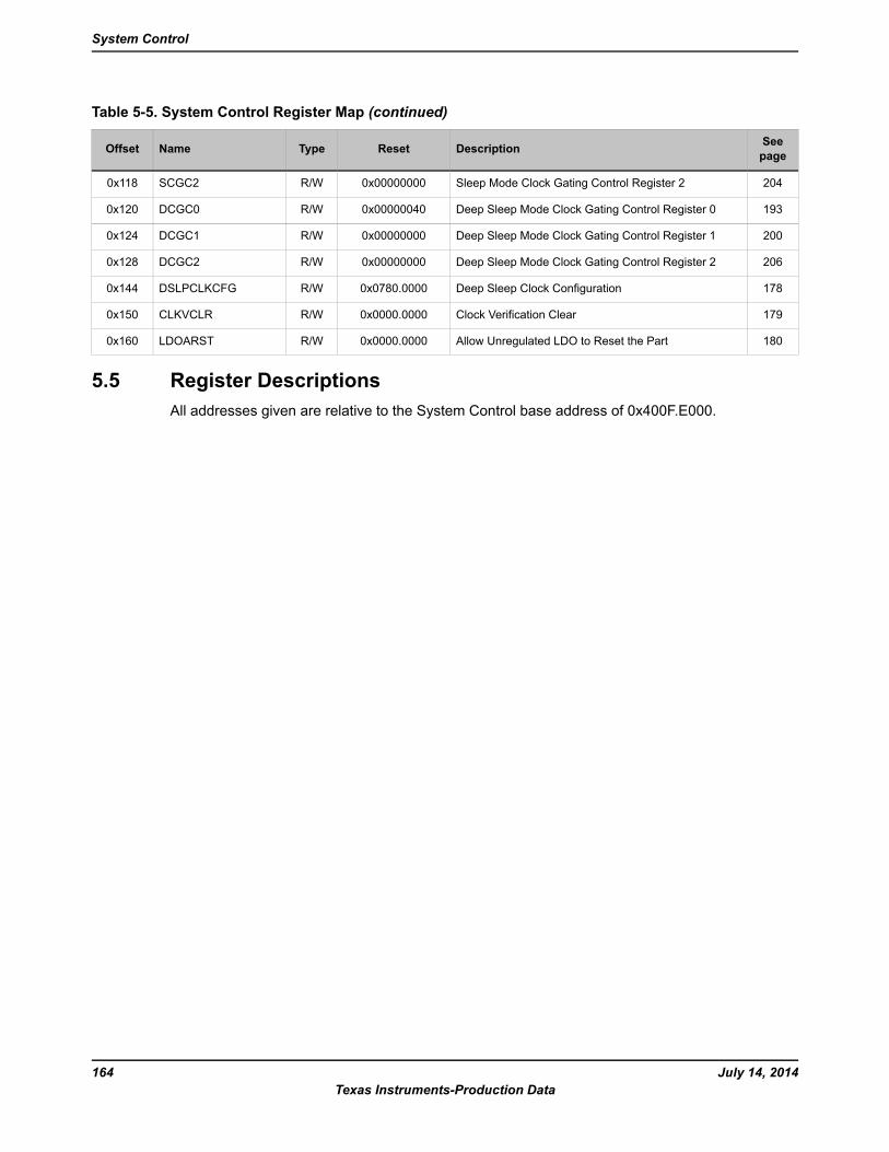
Table 5-5. System Control Register Map (continued)
SeepageDescriptionResetTypeNameOffset
204Sleep Mode Clock Gating Control Register 20x00000000R/WSCGC20x118
193Deep Sleep Mode Clock Gating Control Register 00x00000040R/WDCGC00x120
200Deep Sleep Mode Clock Gating Control Register 10x00000000R/WDCGC10x124
206Deep Sleep Mode Clock Gating Control Register 20x00000000R/WDCGC20x128
178Deep Sleep Clock Configuration0x0780.0000R/WDSLPCLKCFG0x144
179Clock Verification Clear0x0000.0000R/WCLKVCLR0x150
180Allow Unregulated LDO to Reset the Part0x0000.0000R/WLDOARST0x160
5.5 Register DescriptionsAll addresses given are relative to the System Control base address of 0x400F.E000.
July 14, 2014164Texas Instruments-Production Data
System Control
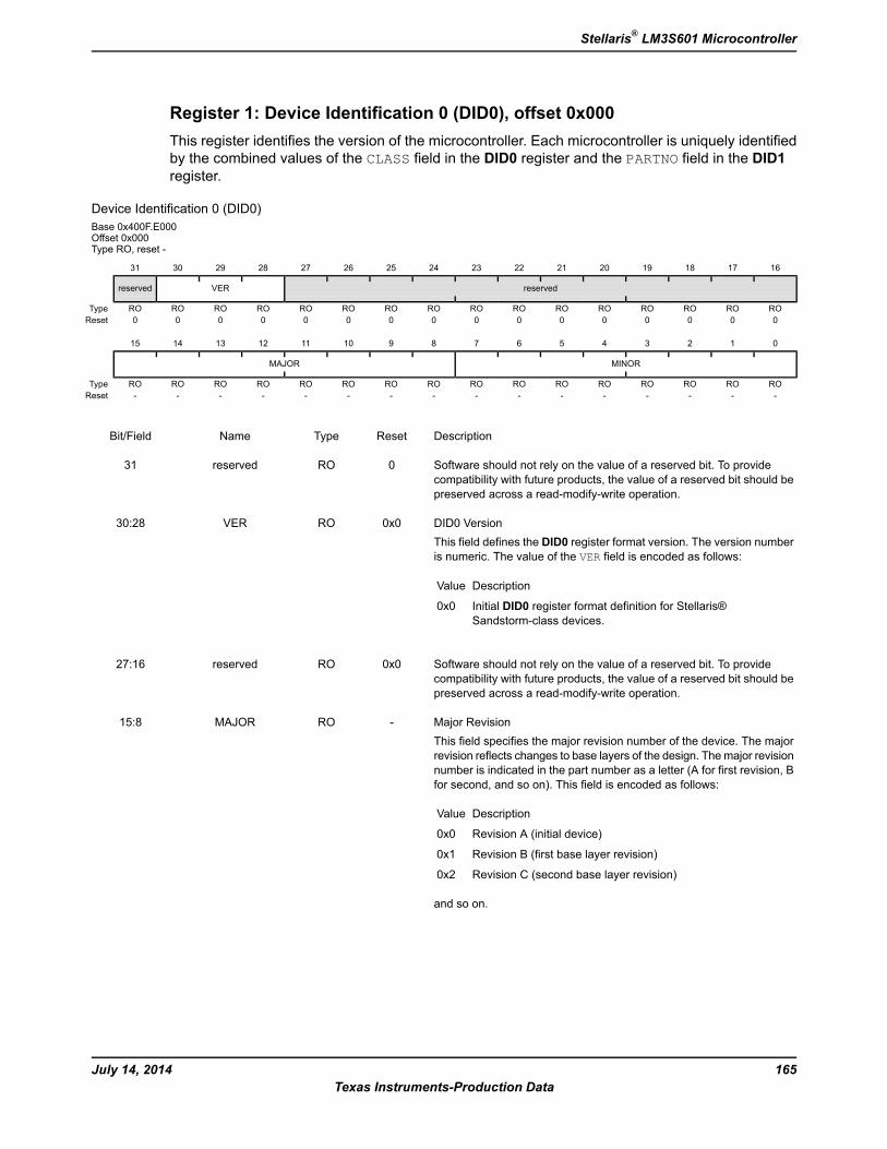
Register 1: Device Identification 0 (DID0), offset 0x000This register identifies the version of the microcontroller. Each microcontroller is uniquely identifiedby the combined values of the CLASS field in the DID0 register and the PARTNO field in the DID1register.
Device Identification 0 (DID0)Base 0x400F.E000Offset 0x000Type RO, reset -
16171819202122232425262728293031
reservedVERreserved
ROROROROROROROROROROROROROROROROType0000000000000000Reset
0123456789101112131415
MINORMAJOR
ROROROROROROROROROROROROROROROROType----------------Reset
DescriptionResetTypeNameBit/Field
Software should not rely on the value of a reserved bit. To providecompatibility with future products, the value of a reserved bit should bepreserved across a read-modify-write operation.
0ROreserved31
DID0 VersionThis field defines the DID0 register format version. The version numberis numeric. The value of the VER field is encoded as follows:
DescriptionValue
Initial DID0 register format definition for Stellaris®Sandstorm-class devices.
0x0
0x0ROVER30:28
Software should not rely on the value of a reserved bit. To providecompatibility with future products, the value of a reserved bit should bepreserved across a read-modify-write operation.
0x0ROreserved27:16
Major RevisionThis field specifies the major revision number of the device. The majorrevision reflects changes to base layers of the design. Themajor revisionnumber is indicated in the part number as a letter (A for first revision, Bfor second, and so on). This field is encoded as follows:
DescriptionValue
Revision A (initial device)0x0
Revision B (first base layer revision)0x1
Revision C (second base layer revision)0x2
and so on.
-ROMAJOR15:8
165July 14, 2014Texas Instruments-Production Data
Stellaris® LM3S601 Microcontroller
DescriptionResetTypeNameBit/Field
Minor RevisionThis field specifies the minor revision number of the device. The minorrevision reflects changes to the metal layers of the design. The MINORfield value is reset when the MAJOR field is changed. This field is numericand is encoded as follows:
DescriptionValue
Initial device, or a major revision update.0x0
First metal layer change.0x1
Second metal layer change.0x2
and so on.
-ROMINOR7:0
July 14, 2014166Texas Instruments-Production Data
System Control
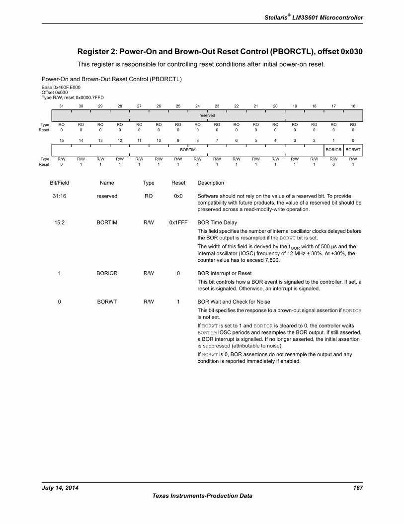
Register 2: Power-On and Brown-Out Reset Control (PBORCTL), offset 0x030This register is responsible for controlling reset conditions after initial power-on reset.
Power-On and Brown-Out Reset Control (PBORCTL)Base 0x400F.E000Offset 0x030Type R/W, reset 0x0000.7FFD
16171819202122232425262728293031
reserved
ROROROROROROROROROROROROROROROROType0000000000000000Reset
0123456789101112131415
BORWTBORIORBORTIM
R/WR/WR/WR/WR/WR/WR/WR/WR/WR/WR/WR/WR/WR/WR/WR/WType1011111111111110Reset
DescriptionResetTypeNameBit/Field
Software should not rely on the value of a reserved bit. To providecompatibility with future products, the value of a reserved bit should bepreserved across a read-modify-write operation.
0x0ROreserved31:16
BOR Time DelayThis field specifies the number of internal oscillator clocks delayed beforethe BOR output is resampled if the BORWT bit is set.The width of this field is derived by the t BOR width of 500 μs and theinternal oscillator (IOSC) frequency of 12 MHz ± 30%. At +30%, thecounter value has to exceed 7,800.
0x1FFFR/WBORTIM15:2
BOR Interrupt or ResetThis bit controls how a BOR event is signaled to the controller. If set, areset is signaled. Otherwise, an interrupt is signaled.
0R/WBORIOR1
BOR Wait and Check for NoiseThis bit specifies the response to a brown-out signal assertion if BORIORis not set.If BORWT is set to 1 and BORIOR is cleared to 0, the controller waitsBORTIM IOSC periods and resamples the BOR output. If still asserted,a BOR interrupt is signalled. If no longer asserted, the initial assertionis suppressed (attributable to noise).If BORWT is 0, BOR assertions do not resample the output and anycondition is reported immediately if enabled.
1R/WBORWT0
167July 14, 2014Texas Instruments-Production Data
Stellaris® LM3S601 Microcontroller
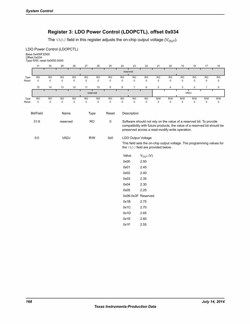
Register 3: LDO Power Control (LDOPCTL), offset 0x034The VADJ field in this register adjusts the on-chip output voltage (VOUT).
LDO Power Control (LDOPCTL)Base 0x400F.E000Offset 0x034Type R/W, reset 0x0000.0000
16171819202122232425262728293031
reserved
ROROROROROROROROROROROROROROROROType0000000000000000Reset
0123456789101112131415
VADJreserved
R/WR/WR/WR/WR/WR/WROROROROROROROROROROType0000000000000000Reset
DescriptionResetTypeNameBit/Field
Software should not rely on the value of a reserved bit. To providecompatibility with future products, the value of a reserved bit should bepreserved across a read-modify-write operation.
0ROreserved31:6
LDO Output VoltageThis field sets the on-chip output voltage. The programming values forthe VADJ field are provided below.
VOUT (V)Value
2.500x00
2.450x01
2.400x02
2.350x03
2.300x04
2.250x05
Reserved0x06-0x3F
2.750x1B
2.700x1C
2.650x1D
2.600x1E
2.550x1F
0x0R/WVADJ5:0
July 14, 2014168Texas Instruments-Production Data
System Control
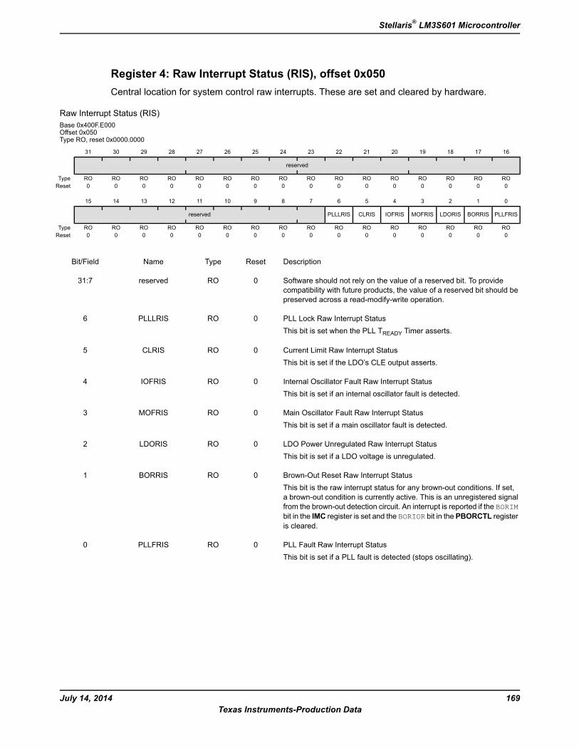
Register 4: Raw Interrupt Status (RIS), offset 0x050Central location for system control raw interrupts. These are set and cleared by hardware.
Raw Interrupt Status (RIS)Base 0x400F.E000Offset 0x050Type RO, reset 0x0000.0000
16171819202122232425262728293031
reserved
ROROROROROROROROROROROROROROROROType0000000000000000Reset
0123456789101112131415
PLLFRISBORRISLDORISMOFRISIOFRISCLRISPLLLRISreserved
ROROROROROROROROROROROROROROROROType0000000000000000Reset
DescriptionResetTypeNameBit/Field
Software should not rely on the value of a reserved bit. To providecompatibility with future products, the value of a reserved bit should bepreserved across a read-modify-write operation.
0ROreserved31:7
PLL Lock Raw Interrupt StatusThis bit is set when the PLL TREADY Timer asserts.
0ROPLLLRIS6
Current Limit Raw Interrupt StatusThis bit is set if the LDO’s CLE output asserts.
0ROCLRIS5
Internal Oscillator Fault Raw Interrupt StatusThis bit is set if an internal oscillator fault is detected.
0ROIOFRIS4
Main Oscillator Fault Raw Interrupt StatusThis bit is set if a main oscillator fault is detected.
0ROMOFRIS3
LDO Power Unregulated Raw Interrupt StatusThis bit is set if a LDO voltage is unregulated.
0ROLDORIS2
Brown-Out Reset Raw Interrupt StatusThis bit is the raw interrupt status for any brown-out conditions. If set,a brown-out condition is currently active. This is an unregistered signalfrom the brown-out detection circuit. An interrupt is reported if the BORIMbit in the IMC register is set and the BORIOR bit in the PBORCTL registeris cleared.
0ROBORRIS1
PLL Fault Raw Interrupt StatusThis bit is set if a PLL fault is detected (stops oscillating).
0ROPLLFRIS0
169July 14, 2014Texas Instruments-Production Data
Stellaris® LM3S601 Microcontroller
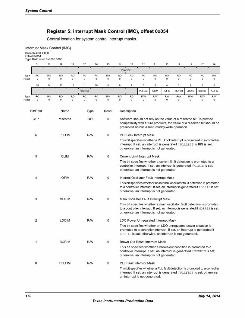
Register 5: Interrupt Mask Control (IMC), offset 0x054Central location for system control interrupt masks.
Interrupt Mask Control (IMC)Base 0x400F.E000Offset 0x054Type R/W, reset 0x0000.0000
16171819202122232425262728293031
reserved
ROROROROROROROROROROROROROROROROType0000000000000000Reset
0123456789101112131415
PLLFIMBORIMLDOIMMOFIMIOFIMCLIMPLLLIMreserved
R/WR/WR/WR/WR/WR/WR/WROROROROROROROROROType0000000000000000Reset
DescriptionResetTypeNameBit/Field
Software should not rely on the value of a reserved bit. To providecompatibility with future products, the value of a reserved bit should bepreserved across a read-modify-write operation.
0ROreserved31:7
PLL Lock Interrupt MaskThis bit specifies whether a PLL Lock interrupt is promoted to a controllerinterrupt. If set, an interrupt is generated if PLLLRIS in RIS is set;otherwise, an interrupt is not generated.
0R/WPLLLIM6
Current Limit Interrupt MaskThis bit specifies whether a current limit detection is promoted to acontroller interrupt. If set, an interrupt is generated if CLRIS is set;otherwise, an interrupt is not generated.
0R/WCLIM5
Internal Oscillator Fault Interrupt MaskThis bit specifies whether an internal oscillator fault detection is promotedto a controller interrupt. If set, an interrupt is generated if IOFRIS is set;otherwise, an interrupt is not generated.
0R/WIOFIM4
Main Oscillator Fault Interrupt MaskThis bit specifies whether a main oscillator fault detection is promotedto a controller interrupt. If set, an interrupt is generated if MOFRIS is set;otherwise, an interrupt is not generated.
0R/WMOFIM3
LDO Power Unregulated Interrupt MaskThis bit specifies whether an LDO unregulated power situation ispromoted to a controller interrupt. If set, an interrupt is generated ifLDORIS is set; otherwise, an interrupt is not generated.
0R/WLDOIM2
Brown-Out Reset Interrupt MaskThis bit specifies whether a brown-out condition is promoted to acontroller interrupt. If set, an interrupt is generated if BORRIS is set;otherwise, an interrupt is not generated.
0R/WBORIM1
PLL Fault Interrupt MaskThis bit specifies whether a PLL fault detection is promoted to a controllerinterrupt. If set, an interrupt is generated if PLLFRIS is set; otherwise,an interrupt is not generated.
0R/WPLLFIM0
July 14, 2014170Texas Instruments-Production Data
System Control
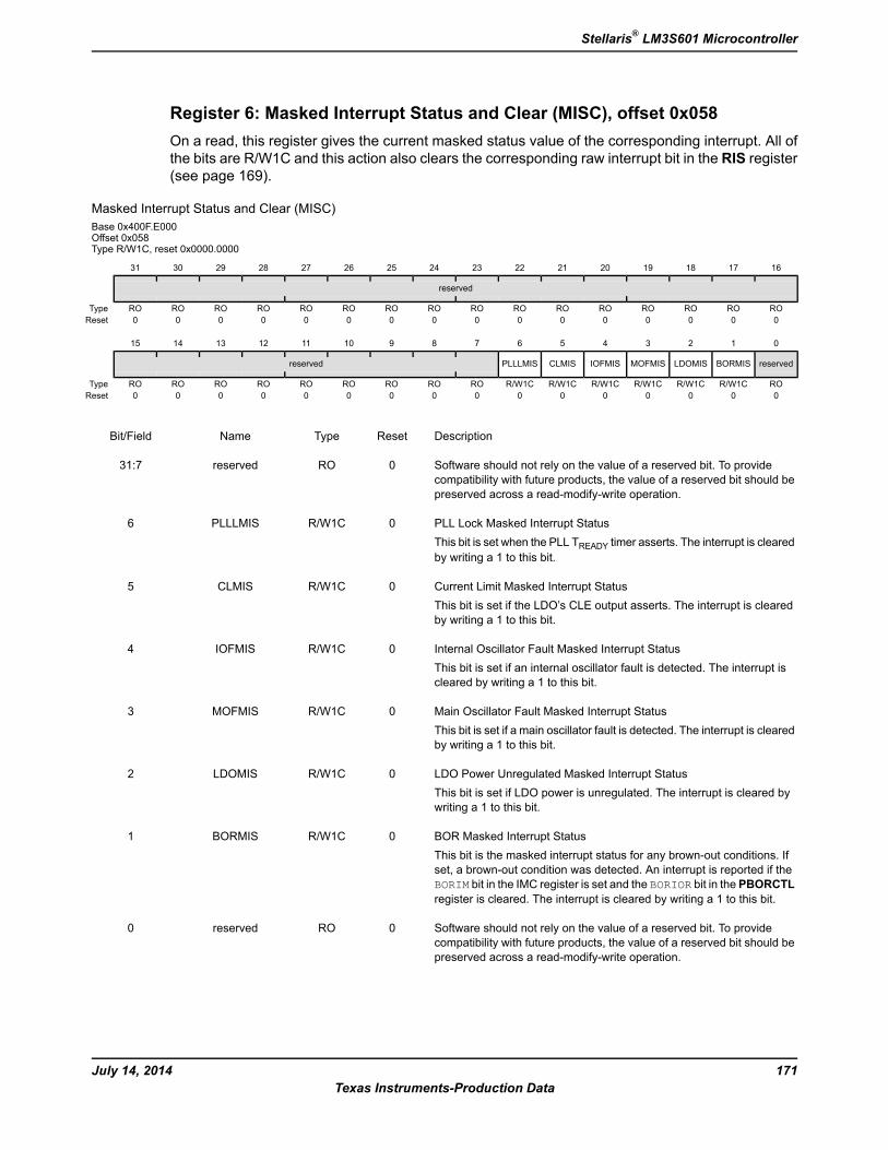
Register 6: Masked Interrupt Status and Clear (MISC), offset 0x058On a read, this register gives the current masked status value of the corresponding interrupt. All ofthe bits are R/W1C and this action also clears the corresponding raw interrupt bit in the RIS register(see page 169).
Masked Interrupt Status and Clear (MISC)Base 0x400F.E000Offset 0x058Type R/W1C, reset 0x0000.0000
16171819202122232425262728293031
reserved
ROROROROROROROROROROROROROROROROType0000000000000000Reset
0123456789101112131415
reservedBORMISLDOMISMOFMISIOFMISCLMISPLLLMISreserved
ROR/W1CR/W1CR/W1CR/W1CR/W1CR/W1CROROROROROROROROROType0000000000000000Reset
DescriptionResetTypeNameBit/Field
Software should not rely on the value of a reserved bit. To providecompatibility with future products, the value of a reserved bit should bepreserved across a read-modify-write operation.
0ROreserved31:7
PLL Lock Masked Interrupt StatusThis bit is set when the PLL TREADY timer asserts. The interrupt is clearedby writing a 1 to this bit.
0R/W1CPLLLMIS6
Current Limit Masked Interrupt StatusThis bit is set if the LDO’s CLE output asserts. The interrupt is clearedby writing a 1 to this bit.
0R/W1CCLMIS5
Internal Oscillator Fault Masked Interrupt StatusThis bit is set if an internal oscillator fault is detected. The interrupt iscleared by writing a 1 to this bit.
0R/W1CIOFMIS4
Main Oscillator Fault Masked Interrupt StatusThis bit is set if a main oscillator fault is detected. The interrupt is clearedby writing a 1 to this bit.
0R/W1CMOFMIS3
LDO Power Unregulated Masked Interrupt StatusThis bit is set if LDO power is unregulated. The interrupt is cleared bywriting a 1 to this bit.
0R/W1CLDOMIS2
BOR Masked Interrupt StatusThis bit is the masked interrupt status for any brown-out conditions. Ifset, a brown-out condition was detected. An interrupt is reported if theBORIM bit in the IMC register is set and the BORIOR bit in the PBORCTLregister is cleared. The interrupt is cleared by writing a 1 to this bit.
0R/W1CBORMIS1
Software should not rely on the value of a reserved bit. To providecompatibility with future products, the value of a reserved bit should bepreserved across a read-modify-write operation.
0ROreserved0
171July 14, 2014Texas Instruments-Production Data
Stellaris® LM3S601 Microcontroller
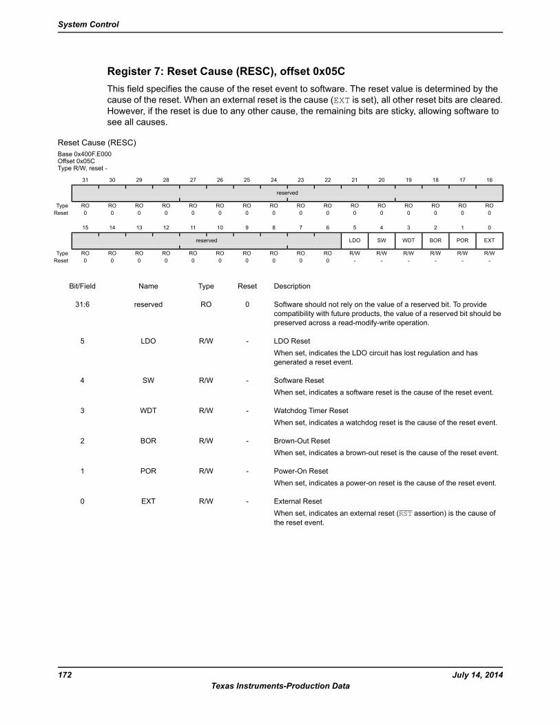
Register 7: Reset Cause (RESC), offset 0x05CThis field specifies the cause of the reset event to software. The reset value is determined by thecause of the reset. When an external reset is the cause (EXT is set), all other reset bits are cleared.However, if the reset is due to any other cause, the remaining bits are sticky, allowing software tosee all causes.
Reset Cause (RESC)Base 0x400F.E000Offset 0x05CType R/W, reset -
16171819202122232425262728293031
reserved
ROROROROROROROROROROROROROROROROType0000000000000000Reset
0123456789101112131415
EXTPORBORWDTSWLDOreserved
R/WR/WR/WR/WR/WR/WROROROROROROROROROROType------0000000000Reset
DescriptionResetTypeNameBit/Field
Software should not rely on the value of a reserved bit. To providecompatibility with future products, the value of a reserved bit should bepreserved across a read-modify-write operation.
0ROreserved31:6
LDO ResetWhen set, indicates the LDO circuit has lost regulation and hasgenerated a reset event.
-R/WLDO5
Software ResetWhen set, indicates a software reset is the cause of the reset event.
-R/WSW4
Watchdog Timer ResetWhen set, indicates a watchdog reset is the cause of the reset event.
-R/WWDT3
Brown-Out ResetWhen set, indicates a brown-out reset is the cause of the reset event.
-R/WBOR2
Power-On ResetWhen set, indicates a power-on reset is the cause of the reset event.
-R/WPOR1
External ResetWhen set, indicates an external reset (RST assertion) is the cause ofthe reset event.
-R/WEXT0
July 14, 2014172Texas Instruments-Production Data
System Control
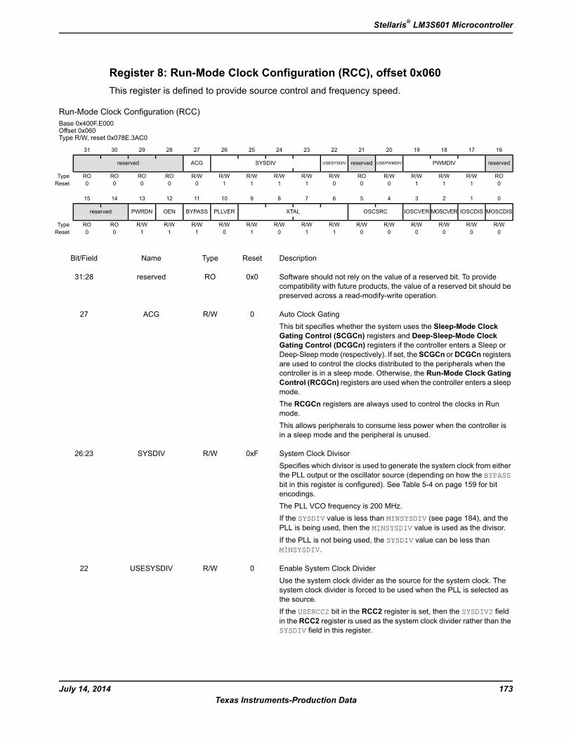
Register 8: Run-Mode Clock Configuration (RCC), offset 0x060This register is defined to provide source control and frequency speed.
Run-Mode Clock Configuration (RCC)Base 0x400F.E000Offset 0x060Type R/W, reset 0x078E.3AC0
16171819202122232425262728293031
reservedPWMDIVUSEPWMDIVreservedUSESYSDIVSYSDIVACGreserved
ROR/WR/WR/WR/WROR/WR/WR/WR/WR/WR/WROROROROType0111000111100000Reset
0123456789101112131415
MOSCDISIOSCDISMOSCVERIOSCVEROSCSRCXTALPLLVERBYPASSOENPWRDNreserved
R/WR/WR/WR/WR/WR/WR/WR/WR/WR/WR/WR/WR/WR/WROROType0000001101011100Reset
DescriptionResetTypeNameBit/Field
Software should not rely on the value of a reserved bit. To providecompatibility with future products, the value of a reserved bit should bepreserved across a read-modify-write operation.
0x0ROreserved31:28
Auto Clock GatingThis bit specifies whether the system uses the Sleep-Mode ClockGating Control (SCGCn) registers and Deep-Sleep-Mode ClockGating Control (DCGCn) registers if the controller enters a Sleep orDeep-Sleep mode (respectively). If set, the SCGCn orDCGCn registersare used to control the clocks distributed to the peripherals when thecontroller is in a sleep mode. Otherwise, the Run-Mode Clock GatingControl (RCGCn) registers are used when the controller enters a sleepmode.The RCGCn registers are always used to control the clocks in Runmode.This allows peripherals to consume less power when the controller isin a sleep mode and the peripheral is unused.
0R/WACG27
System Clock DivisorSpecifies which divisor is used to generate the system clock from eitherthe PLL output or the oscillator source (depending on how the BYPASSbit in this register is configured). See Table 5-4 on page 159 for bitencodings.The PLL VCO frequency is 200 MHz.If the SYSDIV value is less than MINSYSDIV (see page 184), and thePLL is being used, then the MINSYSDIV value is used as the divisor.If the PLL is not being used, the SYSDIV value can be less thanMINSYSDIV.
0xFR/WSYSDIV26:23
Enable System Clock DividerUse the system clock divider as the source for the system clock. Thesystem clock divider is forced to be used when the PLL is selected asthe source.If the USERCC2 bit in the RCC2 register is set, then the SYSDIV2 fieldin the RCC2 register is used as the system clock divider rather than theSYSDIV field in this register.
0R/WUSESYSDIV22
173July 14, 2014Texas Instruments-Production Data
Stellaris® LM3S601 Microcontroller
DescriptionResetTypeNameBit/Field
Software should not rely on the value of a reserved bit. To providecompatibility with future products, the value of a reserved bit should bepreserved across a read-modify-write operation.
0ROreserved21
Enable PWM Clock DivisorUse the PWM clock divider as the source for the PWM clock.
0R/WUSEPWMDIV20
PWM Unit Clock DivisorThis field specifies the binary divisor used to predivide the system clockdown for use as the timing reference for the PWM module. This clockis only power 2 divide and rising edge is synchronous without phaseshift from the system clock.
DivisorValue
/20x0
/40x1
/80x2
/160x3
/320x4
/640x5
/640x6
/64 (default)0x7
0x7R/WPWMDIV19:17
Software should not rely on the value of a reserved bit. To providecompatibility with future products, the value of a reserved bit should bepreserved across a read-modify-write operation.
0ROreserved16:14
PLL Power DownThis bit connects to the PLL PWRDN input. The reset value of 1 powersdown the PLL. See Table 5-6 on page 176 for PLL mode control.
1R/WPWRDN13
PLL Output EnableThis bit specifies whether the PLL output driver is enabled. If cleared,the driver transmits the PLL clock to the output. Otherwise, the PLLclock does not oscillate outside the PLL module.
Note: Both PWRDN and OEN must be cleared to run the PLL.
1R/WOEN12
PLL BypassChooses whether the system clock is derived from the PLL output orthe OSC source. If set, the clock that drives the system is the OSCsource. Otherwise, the clock that drives the system is the PLL outputclock divided by the system divider.See Table 5-4 on page 159 for programming guidelines.
1R/WBYPASS11
PLL VerificationThis bit controls the PLL verification timer function. If set, the verificationtimer is enabled and an interrupt is generated if the PLL becomesinoperative. Otherwise, the verification timer is not enabled.
0R/WPLLVER10
July 14, 2014174Texas Instruments-Production Data
System Control
DescriptionResetTypeNameBit/Field
Crystal ValueThis field specifies the crystal value attached to the main oscillator. Theencoding for this field is provided below.
Crystal Frequency (MHz) Usingthe PLL
Crystal Frequency (MHz) NotUsing the PLL
Value
reserved1.0000x0
reserved1.84320x1
reserved2.0000x2
reserved2.45760x3
3.579545 MHz0x4
3.6864 MHz0x5
4 MHz0x6
4.096 MHz0x7
4.9152 MHz0x8
5 MHz0x9
5.12 MHz0xA
6 MHz (reset value)0xB
6.144 MHz0xC
7.3728 MHz0xD
8 MHz0xE
8.192 MHz0xF
0xBR/WXTAL9:6
Oscillator SourceSelects the input source for the OSC. The values are:
Input SourceValue
MOSCMain oscillator (default)
0x0
IOSCInternal oscillator
0x1
IOSC/4Internal oscillator / 4 (this is necessary if used as input to PLL)
0x2
reserved0x3
0x0R/WOSCSRC5:4
Internal Oscillator Verification TimerThis bit controls the internal oscillator verification timer function. If set,the verification timer is enabled and an interrupt is generated if the timerbecomes inoperative. Otherwise, the verification timer is not enabled.
0R/WIOSCVER3
Main Oscillator Verification TimerThis bit controls the main oscillator verification timer function. If set, theverification timer is enabled and an interrupt is generated if the timerbecomes inoperative. Otherwise, the verification timer is not enabled.
0R/WMOSCVER2
175July 14, 2014Texas Instruments-Production Data
Stellaris® LM3S601 Microcontroller
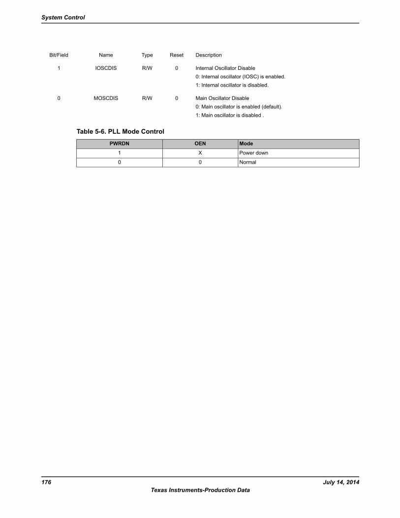
DescriptionResetTypeNameBit/Field
Internal Oscillator Disable0: Internal oscillator (IOSC) is enabled.1: Internal oscillator is disabled.
0R/WIOSCDIS1
Main Oscillator Disable0: Main oscillator is enabled (default).1: Main oscillator is disabled .
0R/WMOSCDIS0
Table 5-6. PLL Mode Control
ModeOENPWRDN
Power downX1
Normal00
July 14, 2014176Texas Instruments-Production Data
System Control
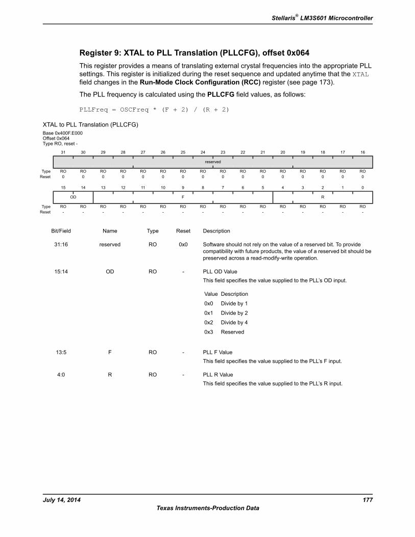
Register 9: XTAL to PLL Translation (PLLCFG), offset 0x064This register provides a means of translating external crystal frequencies into the appropriate PLLsettings. This register is initialized during the reset sequence and updated anytime that the XTALfield changes in the Run-Mode Clock Configuration (RCC) register (see page 173).
The PLL frequency is calculated using the PLLCFG field values, as follows:
PLLFreq = OSCFreq * (F + 2) / (R + 2)
XTAL to PLL Translation (PLLCFG)Base 0x400F.E000Offset 0x064Type RO, reset -
16171819202122232425262728293031
reserved
ROROROROROROROROROROROROROROROROType0000000000000000Reset
0123456789101112131415
RFOD
ROROROROROROROROROROROROROROROROType----------------Reset
DescriptionResetTypeNameBit/Field
Software should not rely on the value of a reserved bit. To providecompatibility with future products, the value of a reserved bit should bepreserved across a read-modify-write operation.
0x0ROreserved31:16
PLL OD ValueThis field specifies the value supplied to the PLL’s OD input.
DescriptionValue
Divide by 10x0
Divide by 20x1
Divide by 40x2
Reserved0x3
-ROOD15:14
PLL F ValueThis field specifies the value supplied to the PLL’s F input.
-ROF13:5
PLL R ValueThis field specifies the value supplied to the PLL’s R input.
-ROR4:0
177July 14, 2014Texas Instruments-Production Data
Stellaris® LM3S601 Microcontroller
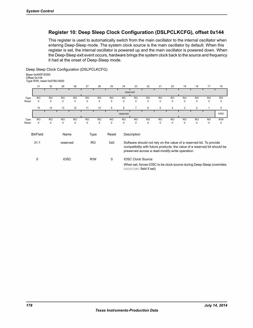
Register 10: Deep Sleep Clock Configuration (DSLPCLKCFG), offset 0x144This register is used to automatically switch from the main oscillator to the internal oscillator whenentering Deep-Sleep mode. The system clock source is the main oscillator by default. When thisregister is set, the internal oscillator is powered up and the main oscillator is powered down. Whenthe Deep-Sleep exit event occurs, hardware brings the system clock back to the source and frequencyit had at the onset of Deep-Sleep mode.
Deep Sleep Clock Configuration (DSLPCLKCFG)Base 0x400F.E000Offset 0x144Type R/W, reset 0x0780.0000
16171819202122232425262728293031
reserved
ROROROROROROROROROROROROROROROROType0000000000000000Reset
0123456789101112131415
IOSCreserved
R/WROROROROROROROROROROROROROROROType0000000000000000Reset
DescriptionResetTypeNameBit/Field
Software should not rely on the value of a reserved bit. To providecompatibility with future products, the value of a reserved bit should bepreserved across a read-modify-write operation.
0x0ROreserved31:1
IOSC Clock SourceWhen set, forces IOSC to be clock source during Deep-Sleep (overridesDSOSCSRC field if set)
0R/WIOSC0
July 14, 2014178Texas Instruments-Production Data
System Control
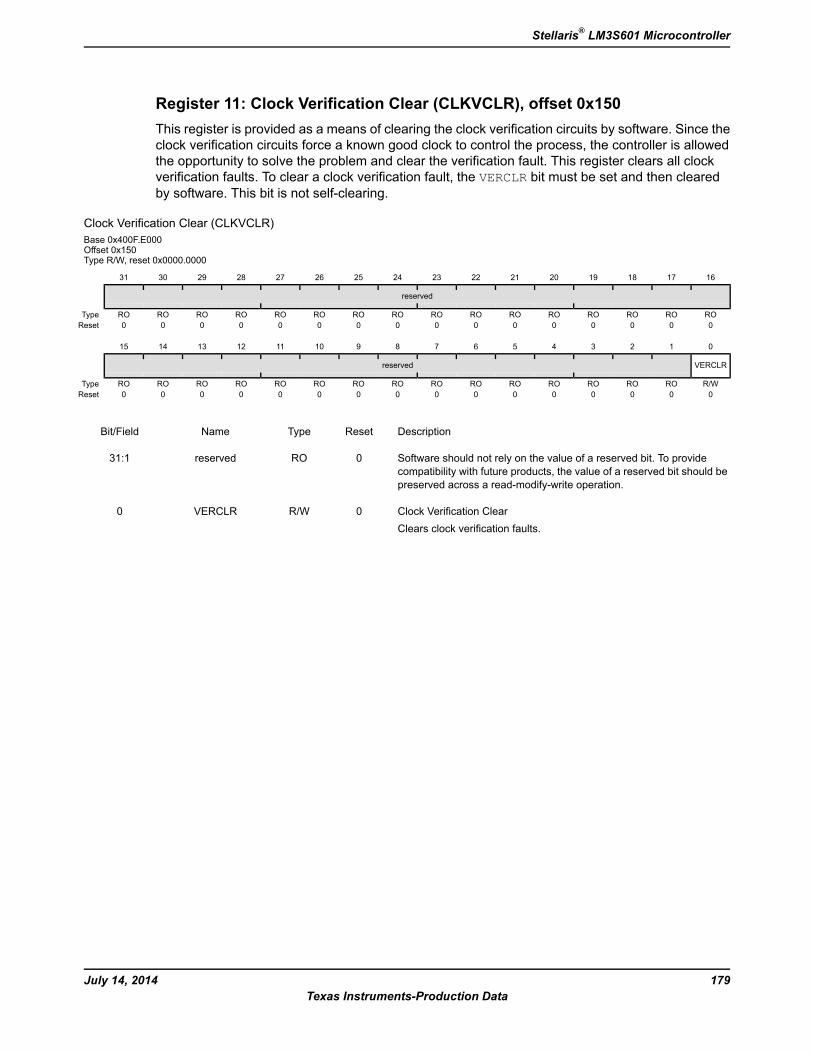
Register 11: Clock Verification Clear (CLKVCLR), offset 0x150This register is provided as a means of clearing the clock verification circuits by software. Since theclock verification circuits force a known good clock to control the process, the controller is allowedthe opportunity to solve the problem and clear the verification fault. This register clears all clockverification faults. To clear a clock verification fault, the VERCLR bit must be set and then clearedby software. This bit is not self-clearing.
Clock Verification Clear (CLKVCLR)Base 0x400F.E000Offset 0x150Type R/W, reset 0x0000.0000
16171819202122232425262728293031
reserved
ROROROROROROROROROROROROROROROROType0000000000000000Reset
0123456789101112131415
VERCLRreserved
R/WROROROROROROROROROROROROROROROType0000000000000000Reset
DescriptionResetTypeNameBit/Field
Software should not rely on the value of a reserved bit. To providecompatibility with future products, the value of a reserved bit should bepreserved across a read-modify-write operation.
0ROreserved31:1
Clock Verification ClearClears clock verification faults.
0R/WVERCLR0
179July 14, 2014Texas Instruments-Production Data
Stellaris® LM3S601 Microcontroller
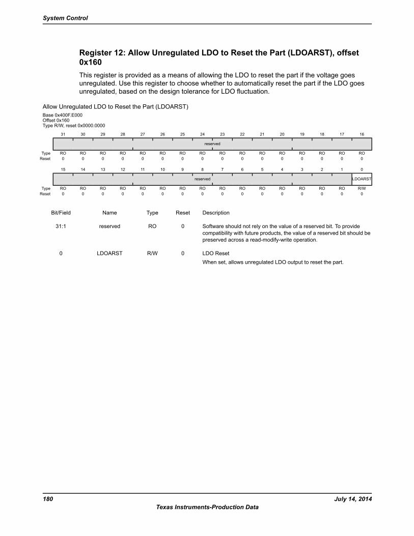
Register 12: Allow Unregulated LDO to Reset the Part (LDOARST), offset0x160This register is provided as a means of allowing the LDO to reset the part if the voltage goesunregulated. Use this register to choose whether to automatically reset the part if the LDO goesunregulated, based on the design tolerance for LDO fluctuation.
Allow Unregulated LDO to Reset the Part (LDOARST)Base 0x400F.E000Offset 0x160Type R/W, reset 0x0000.0000
16171819202122232425262728293031
reserved
ROROROROROROROROROROROROROROROROType0000000000000000Reset
0123456789101112131415
LDOARSTreserved
R/WROROROROROROROROROROROROROROROType0000000000000000Reset
DescriptionResetTypeNameBit/Field
Software should not rely on the value of a reserved bit. To providecompatibility with future products, the value of a reserved bit should bepreserved across a read-modify-write operation.
0ROreserved31:1
LDO ResetWhen set, allows unregulated LDO output to reset the part.
0R/WLDOARST0
July 14, 2014180Texas Instruments-Production Data
System Control
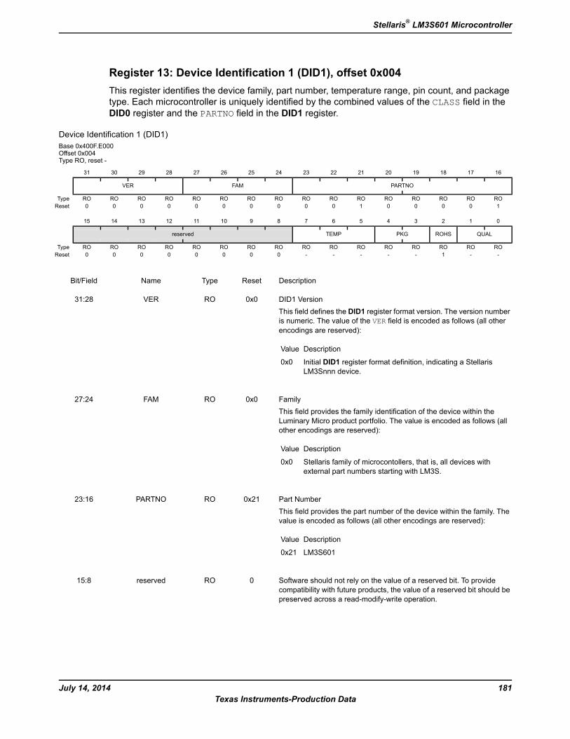
Register 13: Device Identification 1 (DID1), offset 0x004This register identifies the device family, part number, temperature range, pin count, and packagetype. Each microcontroller is uniquely identified by the combined values of the CLASS field in theDID0 register and the PARTNO field in the DID1 register.
Device Identification 1 (DID1)Base 0x400F.E000Offset 0x004Type RO, reset -
16171819202122232425262728293031
PARTNOFAMVER
ROROROROROROROROROROROROROROROROType1000010000000000Reset
0123456789101112131415
QUALROHSPKGTEMPreserved
ROROROROROROROROROROROROROROROROType--1-----00000000Reset
DescriptionResetTypeNameBit/Field
DID1 VersionThis field defines the DID1 register format version. The version numberis numeric. The value of the VER field is encoded as follows (all otherencodings are reserved):
DescriptionValue
Initial DID1 register format definition, indicating a StellarisLM3Snnn device.
0x0
0x0ROVER31:28
FamilyThis field provides the family identification of the device within theLuminary Micro product portfolio. The value is encoded as follows (allother encodings are reserved):
DescriptionValue
Stellaris family of microcontollers, that is, all devices withexternal part numbers starting with LM3S.
0x0
0x0ROFAM27:24
Part NumberThis field provides the part number of the device within the family. Thevalue is encoded as follows (all other encodings are reserved):
DescriptionValue
LM3S6010x21
0x21ROPARTNO23:16
Software should not rely on the value of a reserved bit. To providecompatibility with future products, the value of a reserved bit should bepreserved across a read-modify-write operation.
0ROreserved15:8
181July 14, 2014Texas Instruments-Production Data
Stellaris® LM3S601 Microcontroller
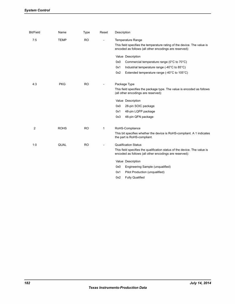
DescriptionResetTypeNameBit/Field
Temperature RangeThis field specifies the temperature rating of the device. The value isencoded as follows (all other encodings are reserved):
DescriptionValue
Commercial temperature range (0°C to 70°C)0x0
Industrial temperature range (-40°C to 85°C)0x1
Extended temperature range (-40°C to 105°C)0x2
-ROTEMP7:5
Package TypeThis field specifies the package type. The value is encoded as follows(all other encodings are reserved):
DescriptionValue
28-pin SOIC package0x0
48-pin LQFP package0x1
48-pin QFN package0x3
-ROPKG4:3
RoHS-ComplianceThis bit specifies whether the device is RoHS-compliant. A 1 indicatesthe part is RoHS-compliant.
1ROROHS2
Qualification StatusThis field specifies the qualification status of the device. The value isencoded as follows (all other encodings are reserved):
DescriptionValue
Engineering Sample (unqualified)0x0
Pilot Production (unqualified)0x1
Fully Qualified0x2
-ROQUAL1:0
July 14, 2014182Texas Instruments-Production Data
System Control
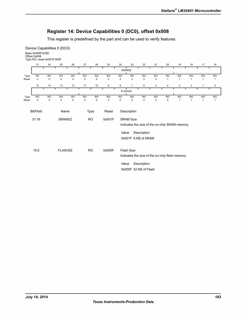
Register 14: Device Capabilities 0 (DC0), offset 0x008This register is predefined by the part and can be used to verify features.
Device Capabilities 0 (DC0)Base 0x400F.E000Offset 0x008Type RO, reset 0x001F.000F
16171819202122232425262728293031
SRAMSZ
ROROROROROROROROROROROROROROROROType1111100000000000Reset
0123456789101112131415
FLASHSZ
ROROROROROROROROROROROROROROROROType1111000000000000Reset
DescriptionResetTypeNameBit/Field
SRAM SizeIndicates the size of the on-chip SRAM memory.
DescriptionValue
8 KB of SRAM0x001F
0x001FROSRAMSZ31:16
Flash SizeIndicates the size of the on-chip flash memory.
DescriptionValue
32 KB of Flash0x000F
0x000FROFLASHSZ15:0
183July 14, 2014Texas Instruments-Production Data
Stellaris® LM3S601 Microcontroller
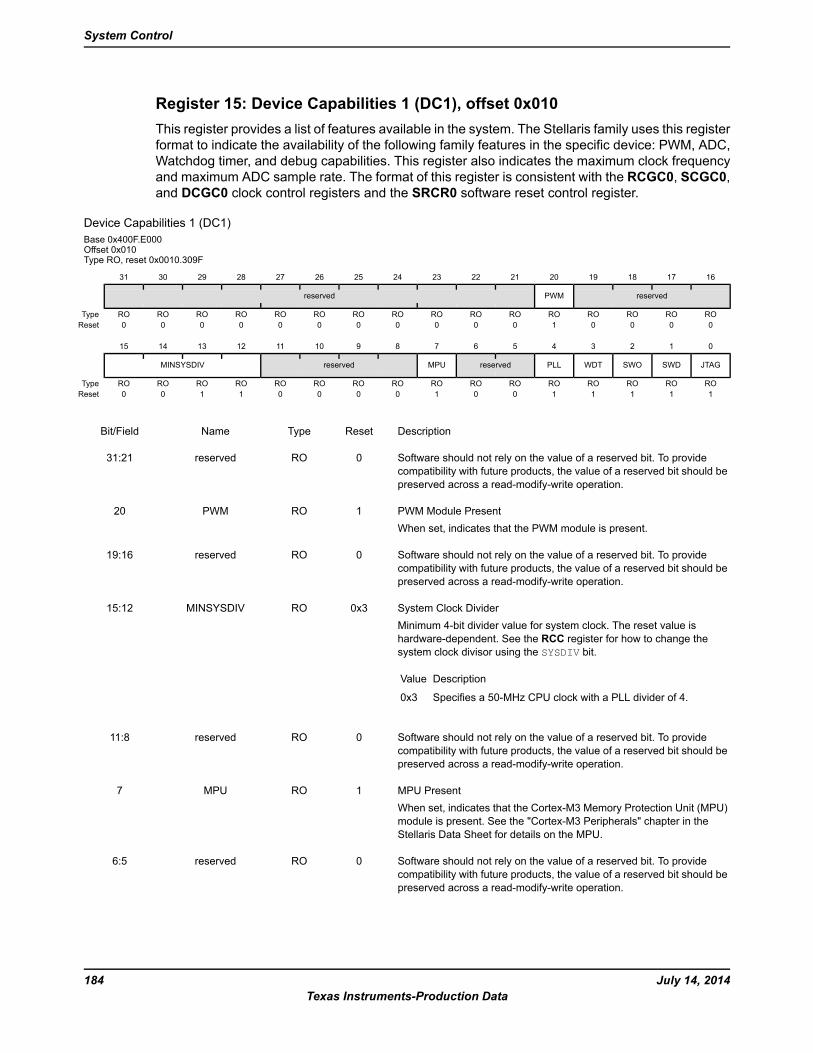
Register 15: Device Capabilities 1 (DC1), offset 0x010This register provides a list of features available in the system. The Stellaris family uses this registerformat to indicate the availability of the following family features in the specific device: PWM, ADC,Watchdog timer, and debug capabilities. This register also indicates the maximum clock frequencyand maximum ADC sample rate. The format of this register is consistent with the RCGC0, SCGC0,and DCGC0 clock control registers and the SRCR0 software reset control register.
Device Capabilities 1 (DC1)Base 0x400F.E000Offset 0x010Type RO, reset 0x0010.309F
16171819202122232425262728293031
reservedPWMreserved
ROROROROROROROROROROROROROROROROType0000100000000000Reset
0123456789101112131415
JTAGSWDSWOWDTPLLreservedMPUreservedMINSYSDIV
ROROROROROROROROROROROROROROROROType1111100100001100Reset
DescriptionResetTypeNameBit/Field
Software should not rely on the value of a reserved bit. To providecompatibility with future products, the value of a reserved bit should bepreserved across a read-modify-write operation.
0ROreserved31:21
PWM Module PresentWhen set, indicates that the PWM module is present.
1ROPWM20
Software should not rely on the value of a reserved bit. To providecompatibility with future products, the value of a reserved bit should bepreserved across a read-modify-write operation.
0ROreserved19:16
System Clock DividerMinimum 4-bit divider value for system clock. The reset value ishardware-dependent. See the RCC register for how to change thesystem clock divisor using the SYSDIV bit.
DescriptionValue
Specifies a 50-MHz CPU clock with a PLL divider of 4.0x3
0x3ROMINSYSDIV15:12
Software should not rely on the value of a reserved bit. To providecompatibility with future products, the value of a reserved bit should bepreserved across a read-modify-write operation.
0ROreserved11:8
MPU PresentWhen set, indicates that the Cortex-M3 Memory Protection Unit (MPU)module is present. See the "Cortex-M3 Peripherals" chapter in theStellaris Data Sheet for details on the MPU.
1ROMPU7
Software should not rely on the value of a reserved bit. To providecompatibility with future products, the value of a reserved bit should bepreserved across a read-modify-write operation.
0ROreserved6:5
July 14, 2014184Texas Instruments-Production Data
System Control
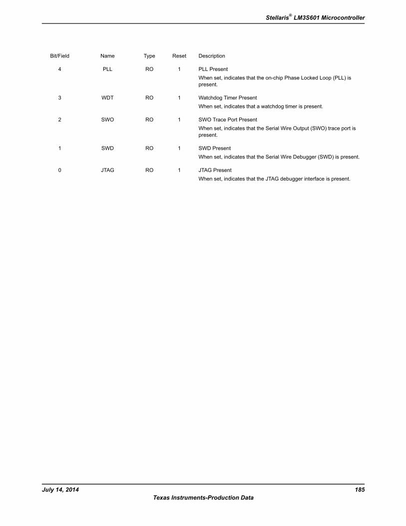
DescriptionResetTypeNameBit/Field
PLL PresentWhen set, indicates that the on-chip Phase Locked Loop (PLL) ispresent.
1ROPLL4
Watchdog Timer PresentWhen set, indicates that a watchdog timer is present.
1ROWDT3
SWO Trace Port PresentWhen set, indicates that the Serial Wire Output (SWO) trace port ispresent.
1ROSWO2
SWD PresentWhen set, indicates that the Serial Wire Debugger (SWD) is present.
1ROSWD1
JTAG PresentWhen set, indicates that the JTAG debugger interface is present.
1ROJTAG0
185July 14, 2014Texas Instruments-Production Data
Stellaris® LM3S601 Microcontroller
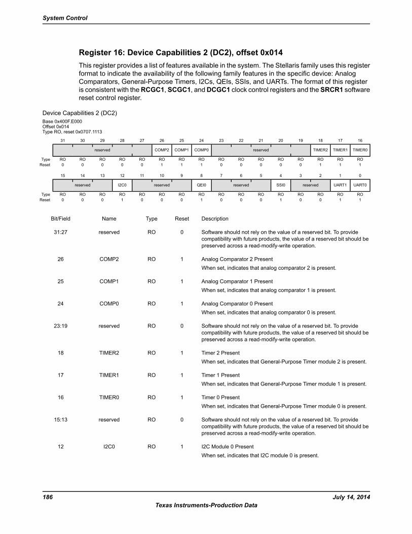
Register 16: Device Capabilities 2 (DC2), offset 0x014This register provides a list of features available in the system. The Stellaris family uses this registerformat to indicate the availability of the following family features in the specific device: AnalogComparators, General-Purpose Timers, I2Cs, QEIs, SSIs, and UARTs. The format of this registeris consistent with theRCGC1, SCGC1, andDCGC1 clock control registers and theSRCR1 softwarereset control register.
Device Capabilities 2 (DC2)Base 0x400F.E000Offset 0x014Type RO, reset 0x0707.1113
16171819202122232425262728293031
TIMER0TIMER1TIMER2reservedCOMP0COMP1COMP2reserved
ROROROROROROROROROROROROROROROROType1110000011100000Reset
0123456789101112131415
UART0UART1reservedSSI0reservedQEI0reservedI2C0reserved
ROROROROROROROROROROROROROROROROType1100100010001000Reset
DescriptionResetTypeNameBit/Field
Software should not rely on the value of a reserved bit. To providecompatibility with future products, the value of a reserved bit should bepreserved across a read-modify-write operation.
0ROreserved31:27
Analog Comparator 2 PresentWhen set, indicates that analog comparator 2 is present.
1ROCOMP226
Analog Comparator 1 PresentWhen set, indicates that analog comparator 1 is present.
1ROCOMP125
Analog Comparator 0 PresentWhen set, indicates that analog comparator 0 is present.
1ROCOMP024
Software should not rely on the value of a reserved bit. To providecompatibility with future products, the value of a reserved bit should bepreserved across a read-modify-write operation.
0ROreserved23:19
Timer 2 PresentWhen set, indicates that General-Purpose Timer module 2 is present.
1ROTIMER218
Timer 1 PresentWhen set, indicates that General-Purpose Timer module 1 is present.
1ROTIMER117
Timer 0 PresentWhen set, indicates that General-Purpose Timer module 0 is present.
1ROTIMER016
Software should not rely on the value of a reserved bit. To providecompatibility with future products, the value of a reserved bit should bepreserved across a read-modify-write operation.
0ROreserved15:13
I2C Module 0 PresentWhen set, indicates that I2C module 0 is present.
1ROI2C012
July 14, 2014186Texas Instruments-Production Data
System Control
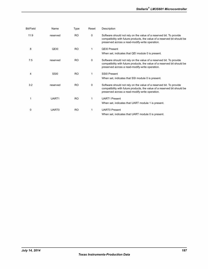
DescriptionResetTypeNameBit/Field
Software should not rely on the value of a reserved bit. To providecompatibility with future products, the value of a reserved bit should bepreserved across a read-modify-write operation.
0ROreserved11:9
QEI0 PresentWhen set, indicates that QEI module 0 is present.
1ROQEI08
Software should not rely on the value of a reserved bit. To providecompatibility with future products, the value of a reserved bit should bepreserved across a read-modify-write operation.
0ROreserved7:5
SSI0 PresentWhen set, indicates that SSI module 0 is present.
1ROSSI04
Software should not rely on the value of a reserved bit. To providecompatibility with future products, the value of a reserved bit should bepreserved across a read-modify-write operation.
0ROreserved3:2
UART1 PresentWhen set, indicates that UART module 1 is present.
1ROUART11
UART0 PresentWhen set, indicates that UART module 0 is present.
1ROUART00
187July 14, 2014Texas Instruments-Production Data
Stellaris® LM3S601 Microcontroller
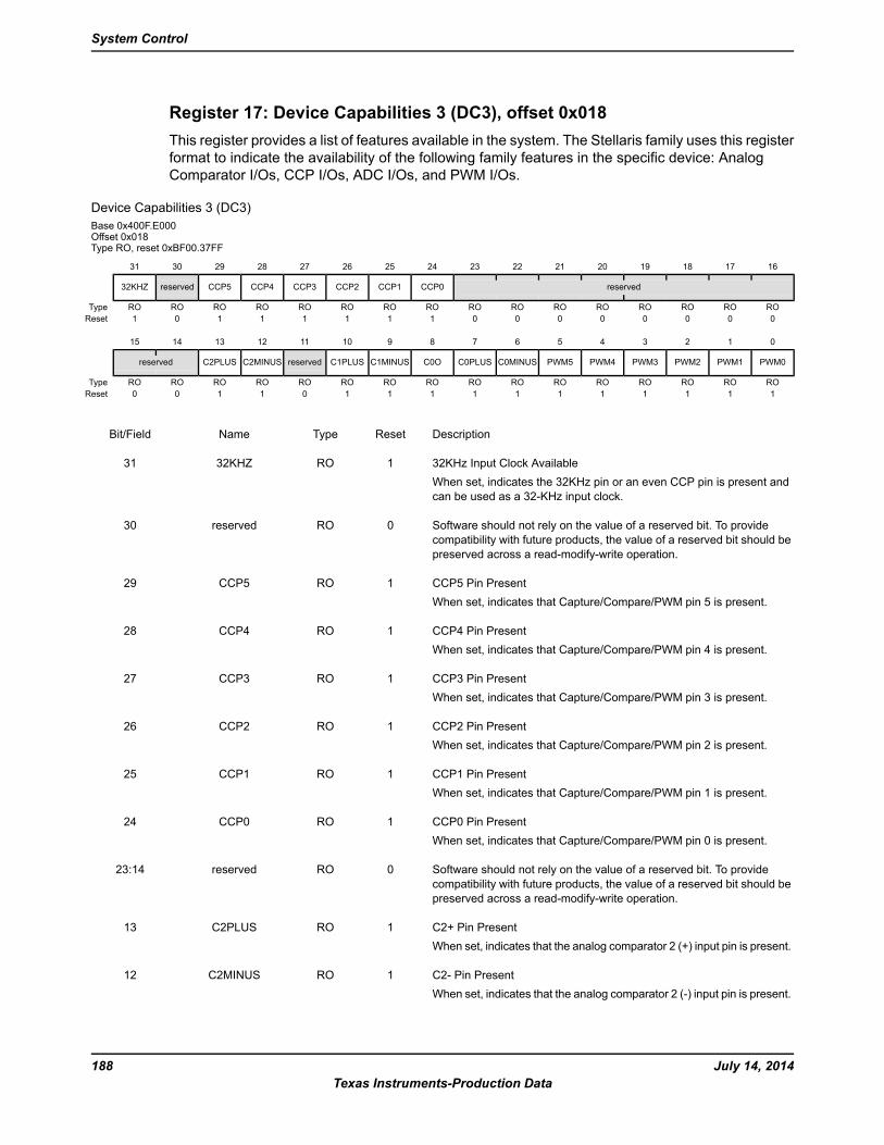
Register 17: Device Capabilities 3 (DC3), offset 0x018This register provides a list of features available in the system. The Stellaris family uses this registerformat to indicate the availability of the following family features in the specific device: AnalogComparator I/Os, CCP I/Os, ADC I/Os, and PWM I/Os.
Device Capabilities 3 (DC3)Base 0x400F.E000Offset 0x018Type RO, reset 0xBF00.37FF
16171819202122232425262728293031
reservedCCP0CCP1CCP2CCP3CCP4CCP5reserved32KHZ
ROROROROROROROROROROROROROROROROType0000000011111101Reset
0123456789101112131415
PWM0PWM1PWM2PWM3PWM4PWM5C0MINUSC0PLUSC0OC1MINUSC1PLUSreservedC2MINUSC2PLUSreserved
ROROROROROROROROROROROROROROROROType1111111111101100Reset
DescriptionResetTypeNameBit/Field
32KHz Input Clock AvailableWhen set, indicates the 32KHz pin or an even CCP pin is present andcan be used as a 32-KHz input clock.
1RO32KHZ31
Software should not rely on the value of a reserved bit. To providecompatibility with future products, the value of a reserved bit should bepreserved across a read-modify-write operation.
0ROreserved30
CCP5 Pin PresentWhen set, indicates that Capture/Compare/PWM pin 5 is present.
1ROCCP529
CCP4 Pin PresentWhen set, indicates that Capture/Compare/PWM pin 4 is present.
1ROCCP428
CCP3 Pin PresentWhen set, indicates that Capture/Compare/PWM pin 3 is present.
1ROCCP327
CCP2 Pin PresentWhen set, indicates that Capture/Compare/PWM pin 2 is present.
1ROCCP226
CCP1 Pin PresentWhen set, indicates that Capture/Compare/PWM pin 1 is present.
1ROCCP125
CCP0 Pin PresentWhen set, indicates that Capture/Compare/PWM pin 0 is present.
1ROCCP024
Software should not rely on the value of a reserved bit. To providecompatibility with future products, the value of a reserved bit should bepreserved across a read-modify-write operation.
0ROreserved23:14
C2+ Pin PresentWhen set, indicates that the analog comparator 2 (+) input pin is present.
1ROC2PLUS13
C2- Pin PresentWhen set, indicates that the analog comparator 2 (-) input pin is present.
1ROC2MINUS12
July 14, 2014188Texas Instruments-Production Data
System Control
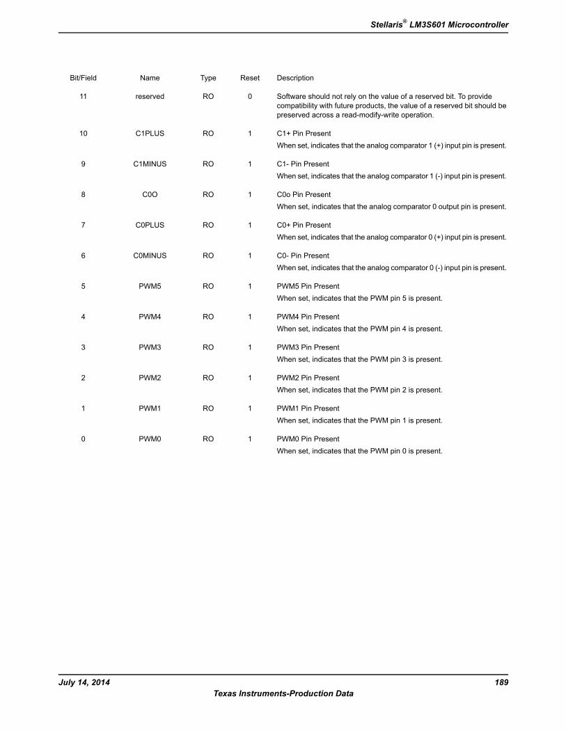
DescriptionResetTypeNameBit/Field
Software should not rely on the value of a reserved bit. To providecompatibility with future products, the value of a reserved bit should bepreserved across a read-modify-write operation.
0ROreserved11
C1+ Pin PresentWhen set, indicates that the analog comparator 1 (+) input pin is present.
1ROC1PLUS10
C1- Pin PresentWhen set, indicates that the analog comparator 1 (-) input pin is present.
1ROC1MINUS9
C0o Pin PresentWhen set, indicates that the analog comparator 0 output pin is present.
1ROC0O8
C0+ Pin PresentWhen set, indicates that the analog comparator 0 (+) input pin is present.
1ROC0PLUS7
C0- Pin PresentWhen set, indicates that the analog comparator 0 (-) input pin is present.
1ROC0MINUS6
PWM5 Pin PresentWhen set, indicates that the PWM pin 5 is present.
1ROPWM55
PWM4 Pin PresentWhen set, indicates that the PWM pin 4 is present.
1ROPWM44
PWM3 Pin PresentWhen set, indicates that the PWM pin 3 is present.
1ROPWM33
PWM2 Pin PresentWhen set, indicates that the PWM pin 2 is present.
1ROPWM22
PWM1 Pin PresentWhen set, indicates that the PWM pin 1 is present.
1ROPWM11
PWM0 Pin PresentWhen set, indicates that the PWM pin 0 is present.
1ROPWM00
189July 14, 2014Texas Instruments-Production Data
Stellaris® LM3S601 Microcontroller
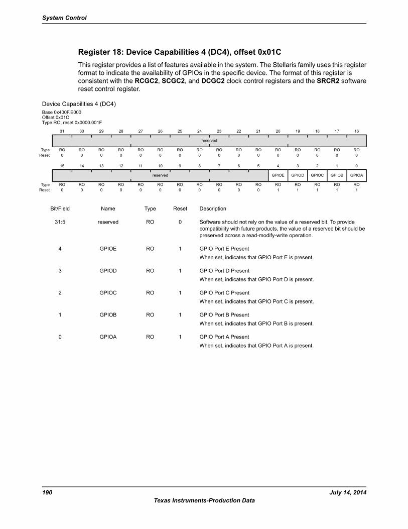
Register 18: Device Capabilities 4 (DC4), offset 0x01CThis register provides a list of features available in the system. The Stellaris family uses this registerformat to indicate the availability of GPIOs in the specific device. The format of this register isconsistent with the RCGC2, SCGC2, and DCGC2 clock control registers and the SRCR2 softwarereset control register.
Device Capabilities 4 (DC4)Base 0x400F.E000Offset 0x01CType RO, reset 0x0000.001F
16171819202122232425262728293031
reserved
ROROROROROROROROROROROROROROROROType0000000000000000Reset
0123456789101112131415
GPIOAGPIOBGPIOCGPIODGPIOEreserved
ROROROROROROROROROROROROROROROROType1111100000000000Reset
DescriptionResetTypeNameBit/Field
Software should not rely on the value of a reserved bit. To providecompatibility with future products, the value of a reserved bit should bepreserved across a read-modify-write operation.
0ROreserved31:5
GPIO Port E PresentWhen set, indicates that GPIO Port E is present.
1ROGPIOE4
GPIO Port D PresentWhen set, indicates that GPIO Port D is present.
1ROGPIOD3
GPIO Port C PresentWhen set, indicates that GPIO Port C is present.
1ROGPIOC2
GPIO Port B PresentWhen set, indicates that GPIO Port B is present.
1ROGPIOB1
GPIO Port A PresentWhen set, indicates that GPIO Port A is present.
1ROGPIOA0
July 14, 2014190Texas Instruments-Production Data
System Control
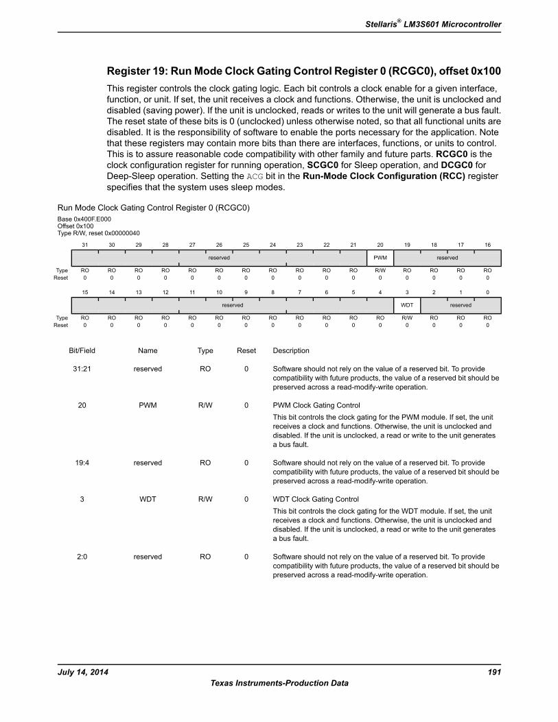
Register 19: RunMode Clock Gating Control Register 0 (RCGC0), offset 0x100This register controls the clock gating logic. Each bit controls a clock enable for a given interface,function, or unit. If set, the unit receives a clock and functions. Otherwise, the unit is unclocked anddisabled (saving power). If the unit is unclocked, reads or writes to the unit will generate a bus fault.The reset state of these bits is 0 (unclocked) unless otherwise noted, so that all functional units aredisabled. It is the responsibility of software to enable the ports necessary for the application. Notethat these registers may contain more bits than there are interfaces, functions, or units to control.This is to assure reasonable code compatibility with other family and future parts. RCGC0 is theclock configuration register for running operation, SCGC0 for Sleep operation, and DCGC0 forDeep-Sleep operation. Setting the ACG bit in the Run-Mode Clock Configuration (RCC) registerspecifies that the system uses sleep modes.
Run Mode Clock Gating Control Register 0 (RCGC0)Base 0x400F.E000Offset 0x100Type R/W, reset 0x00000040
16171819202122232425262728293031
reservedPWMreserved
ROROROROR/WROROROROROROROROROROROType0000000000000000Reset
0123456789101112131415
reservedWDTreserved
ROROROR/WROROROROROROROROROROROROType0000000000000000Reset
DescriptionResetTypeNameBit/Field
Software should not rely on the value of a reserved bit. To providecompatibility with future products, the value of a reserved bit should bepreserved across a read-modify-write operation.
0ROreserved31:21
PWM Clock Gating ControlThis bit controls the clock gating for the PWM module. If set, the unitreceives a clock and functions. Otherwise, the unit is unclocked anddisabled. If the unit is unclocked, a read or write to the unit generatesa bus fault.
0R/WPWM20
Software should not rely on the value of a reserved bit. To providecompatibility with future products, the value of a reserved bit should bepreserved across a read-modify-write operation.
0ROreserved19:4
WDT Clock Gating ControlThis bit controls the clock gating for the WDT module. If set, the unitreceives a clock and functions. Otherwise, the unit is unclocked anddisabled. If the unit is unclocked, a read or write to the unit generatesa bus fault.
0R/WWDT3
Software should not rely on the value of a reserved bit. To providecompatibility with future products, the value of a reserved bit should bepreserved across a read-modify-write operation.
0ROreserved2:0
191July 14, 2014Texas Instruments-Production Data
Stellaris® LM3S601 Microcontroller
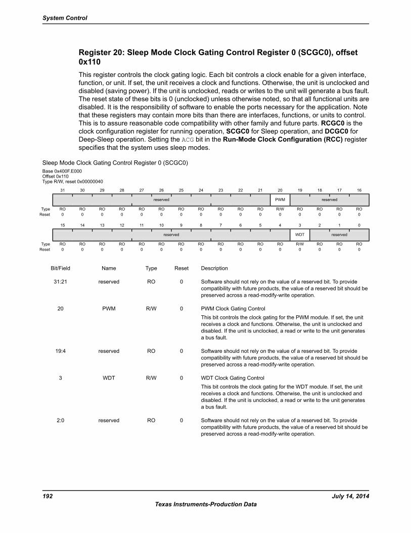
Register 20: Sleep Mode Clock Gating Control Register 0 (SCGC0), offset0x110This register controls the clock gating logic. Each bit controls a clock enable for a given interface,function, or unit. If set, the unit receives a clock and functions. Otherwise, the unit is unclocked anddisabled (saving power). If the unit is unclocked, reads or writes to the unit will generate a bus fault.The reset state of these bits is 0 (unclocked) unless otherwise noted, so that all functional units aredisabled. It is the responsibility of software to enable the ports necessary for the application. Notethat these registers may contain more bits than there are interfaces, functions, or units to control.This is to assure reasonable code compatibility with other family and future parts. RCGC0 is theclock configuration register for running operation, SCGC0 for Sleep operation, and DCGC0 forDeep-Sleep operation. Setting the ACG bit in the Run-Mode Clock Configuration (RCC) registerspecifies that the system uses sleep modes.
Sleep Mode Clock Gating Control Register 0 (SCGC0)Base 0x400F.E000Offset 0x110Type R/W, reset 0x00000040
16171819202122232425262728293031
reservedPWMreserved
ROROROROR/WROROROROROROROROROROROType0000000000000000Reset
0123456789101112131415
reservedWDTreserved
ROROROR/WROROROROROROROROROROROROType0000000000000000Reset
DescriptionResetTypeNameBit/Field
Software should not rely on the value of a reserved bit. To providecompatibility with future products, the value of a reserved bit should bepreserved across a read-modify-write operation.
0ROreserved31:21
PWM Clock Gating ControlThis bit controls the clock gating for the PWM module. If set, the unitreceives a clock and functions. Otherwise, the unit is unclocked anddisabled. If the unit is unclocked, a read or write to the unit generatesa bus fault.
0R/WPWM20
Software should not rely on the value of a reserved bit. To providecompatibility with future products, the value of a reserved bit should bepreserved across a read-modify-write operation.
0ROreserved19:4
WDT Clock Gating ControlThis bit controls the clock gating for the WDT module. If set, the unitreceives a clock and functions. Otherwise, the unit is unclocked anddisabled. If the unit is unclocked, a read or write to the unit generatesa bus fault.
0R/WWDT3
Software should not rely on the value of a reserved bit. To providecompatibility with future products, the value of a reserved bit should bepreserved across a read-modify-write operation.
0ROreserved2:0
July 14, 2014192Texas Instruments-Production Data
System Control
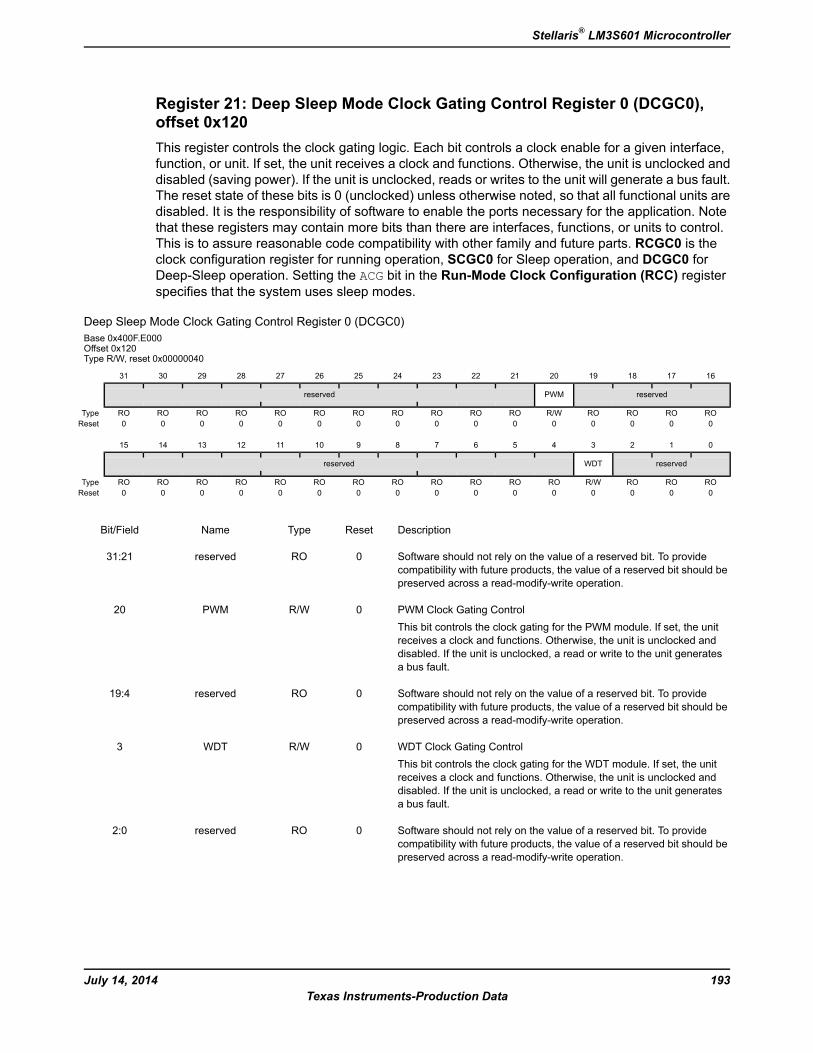
Register 21: Deep Sleep Mode Clock Gating Control Register 0 (DCGC0),offset 0x120This register controls the clock gating logic. Each bit controls a clock enable for a given interface,function, or unit. If set, the unit receives a clock and functions. Otherwise, the unit is unclocked anddisabled (saving power). If the unit is unclocked, reads or writes to the unit will generate a bus fault.The reset state of these bits is 0 (unclocked) unless otherwise noted, so that all functional units aredisabled. It is the responsibility of software to enable the ports necessary for the application. Notethat these registers may contain more bits than there are interfaces, functions, or units to control.This is to assure reasonable code compatibility with other family and future parts. RCGC0 is theclock configuration register for running operation, SCGC0 for Sleep operation, and DCGC0 forDeep-Sleep operation. Setting the ACG bit in the Run-Mode Clock Configuration (RCC) registerspecifies that the system uses sleep modes.
Deep Sleep Mode Clock Gating Control Register 0 (DCGC0)Base 0x400F.E000Offset 0x120Type R/W, reset 0x00000040
16171819202122232425262728293031
reservedPWMreserved
ROROROROR/WROROROROROROROROROROROType0000000000000000Reset
0123456789101112131415
reservedWDTreserved
ROROROR/WROROROROROROROROROROROROType0000000000000000Reset
DescriptionResetTypeNameBit/Field
Software should not rely on the value of a reserved bit. To providecompatibility with future products, the value of a reserved bit should bepreserved across a read-modify-write operation.
0ROreserved31:21
PWM Clock Gating ControlThis bit controls the clock gating for the PWM module. If set, the unitreceives a clock and functions. Otherwise, the unit is unclocked anddisabled. If the unit is unclocked, a read or write to the unit generatesa bus fault.
0R/WPWM20
Software should not rely on the value of a reserved bit. To providecompatibility with future products, the value of a reserved bit should bepreserved across a read-modify-write operation.
0ROreserved19:4
WDT Clock Gating ControlThis bit controls the clock gating for the WDT module. If set, the unitreceives a clock and functions. Otherwise, the unit is unclocked anddisabled. If the unit is unclocked, a read or write to the unit generatesa bus fault.
0R/WWDT3
Software should not rely on the value of a reserved bit. To providecompatibility with future products, the value of a reserved bit should bepreserved across a read-modify-write operation.
0ROreserved2:0
193July 14, 2014Texas Instruments-Production Data
Stellaris® LM3S601 Microcontroller
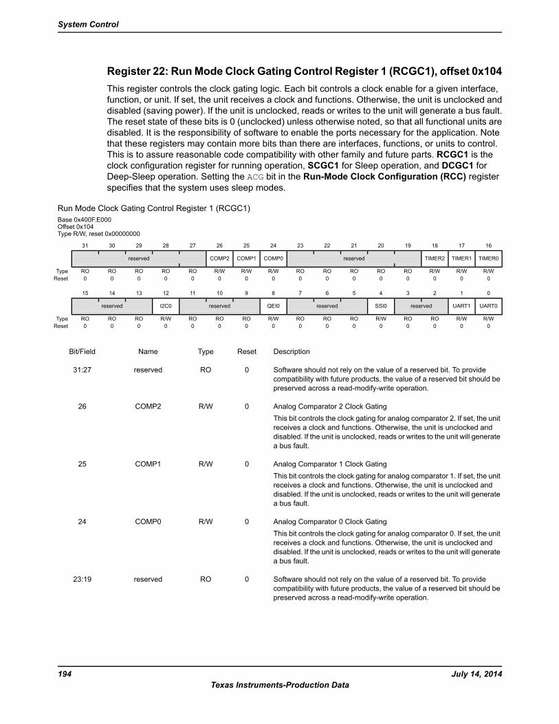
Register 22: RunMode Clock Gating Control Register 1 (RCGC1), offset 0x104This register controls the clock gating logic. Each bit controls a clock enable for a given interface,function, or unit. If set, the unit receives a clock and functions. Otherwise, the unit is unclocked anddisabled (saving power). If the unit is unclocked, reads or writes to the unit will generate a bus fault.The reset state of these bits is 0 (unclocked) unless otherwise noted, so that all functional units aredisabled. It is the responsibility of software to enable the ports necessary for the application. Notethat these registers may contain more bits than there are interfaces, functions, or units to control.This is to assure reasonable code compatibility with other family and future parts. RCGC1 is theclock configuration register for running operation, SCGC1 for Sleep operation, and DCGC1 forDeep-Sleep operation. Setting the ACG bit in the Run-Mode Clock Configuration (RCC) registerspecifies that the system uses sleep modes.
Run Mode Clock Gating Control Register 1 (RCGC1)Base 0x400F.E000Offset 0x104Type R/W, reset 0x00000000
16171819202122232425262728293031
TIMER0TIMER1TIMER2reservedCOMP0COMP1COMP2reserved
R/WR/WR/WROROROROROR/WR/WR/WROROROROROType0000000000000000Reset
0123456789101112131415
UART0UART1reservedSSI0reservedQEI0reservedI2C0reserved
R/WR/WROROR/WROROROR/WROROROR/WROROROType0000000000000000Reset
DescriptionResetTypeNameBit/Field
Software should not rely on the value of a reserved bit. To providecompatibility with future products, the value of a reserved bit should bepreserved across a read-modify-write operation.
0ROreserved31:27
Analog Comparator 2 Clock GatingThis bit controls the clock gating for analog comparator 2. If set, the unitreceives a clock and functions. Otherwise, the unit is unclocked anddisabled. If the unit is unclocked, reads or writes to the unit will generatea bus fault.
0R/WCOMP226
Analog Comparator 1 Clock GatingThis bit controls the clock gating for analog comparator 1. If set, the unitreceives a clock and functions. Otherwise, the unit is unclocked anddisabled. If the unit is unclocked, reads or writes to the unit will generatea bus fault.
0R/WCOMP125
Analog Comparator 0 Clock GatingThis bit controls the clock gating for analog comparator 0. If set, the unitreceives a clock and functions. Otherwise, the unit is unclocked anddisabled. If the unit is unclocked, reads or writes to the unit will generatea bus fault.
0R/WCOMP024
Software should not rely on the value of a reserved bit. To providecompatibility with future products, the value of a reserved bit should bepreserved across a read-modify-write operation.
0ROreserved23:19
July 14, 2014194Texas Instruments-Production Data
System Control

DescriptionResetTypeNameBit/Field
Timer 2 Clock Gating ControlThis bit controls the clock gating for General-Purpose Timer module 2.If set, the unit receives a clock and functions. Otherwise, the unit isunclocked and disabled. If the unit is unclocked, reads or writes to theunit will generate a bus fault.
0R/WTIMER218
Timer 1 Clock Gating ControlThis bit controls the clock gating for General-Purpose Timer module 1.If set, the unit receives a clock and functions. Otherwise, the unit isunclocked and disabled. If the unit is unclocked, reads or writes to theunit will generate a bus fault.
0R/WTIMER117
Timer 0 Clock Gating ControlThis bit controls the clock gating for General-Purpose Timer module 0.If set, the unit receives a clock and functions. Otherwise, the unit isunclocked and disabled. If the unit is unclocked, reads or writes to theunit will generate a bus fault.
0R/WTIMER016
Software should not rely on the value of a reserved bit. To providecompatibility with future products, the value of a reserved bit should bepreserved across a read-modify-write operation.
0ROreserved15:13
I2C0 Clock Gating ControlThis bit controls the clock gating for I2Cmodule 0. If set, the unit receivesa clock and functions. Otherwise, the unit is unclocked and disabled. Ifthe unit is unclocked, reads or writes to the unit will generate a bus fault.
0R/WI2C012
Software should not rely on the value of a reserved bit. To providecompatibility with future products, the value of a reserved bit should bepreserved across a read-modify-write operation.
0ROreserved11:9
QEI0 Clock Gating ControlThis bit controls the clock gating for QEI module 0. If set, the unitreceives a clock and functions. Otherwise, the unit is unclocked anddisabled. If the unit is unclocked, reads or writes to the unit will generatea bus fault.
0R/WQEI08
Software should not rely on the value of a reserved bit. To providecompatibility with future products, the value of a reserved bit should bepreserved across a read-modify-write operation.
0ROreserved7:5
SSI0 Clock Gating ControlThis bit controls the clock gating for SSI module 0. If set, the unit receivesa clock and functions. Otherwise, the unit is unclocked and disabled. Ifthe unit is unclocked, reads or writes to the unit will generate a bus fault.
0R/WSSI04
Software should not rely on the value of a reserved bit. To providecompatibility with future products, the value of a reserved bit should bepreserved across a read-modify-write operation.
0ROreserved3:2
UART1 Clock Gating ControlThis bit controls the clock gating for UART module 1. If set, the unitreceives a clock and functions. Otherwise, the unit is unclocked anddisabled. If the unit is unclocked, reads or writes to the unit will generatea bus fault.
0R/WUART11
195July 14, 2014Texas Instruments-Production Data
Stellaris® LM3S601 Microcontroller

DescriptionResetTypeNameBit/Field
UART0 Clock Gating ControlThis bit controls the clock gating for UART module 0. If set, the unitreceives a clock and functions. Otherwise, the unit is unclocked anddisabled. If the unit is unclocked, reads or writes to the unit will generatea bus fault.
0R/WUART00
July 14, 2014196Texas Instruments-Production Data
System Control
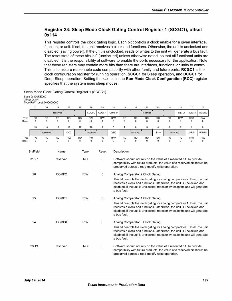
Register 23: Sleep Mode Clock Gating Control Register 1 (SCGC1), offset0x114This register controls the clock gating logic. Each bit controls a clock enable for a given interface,function, or unit. If set, the unit receives a clock and functions. Otherwise, the unit is unclocked anddisabled (saving power). If the unit is unclocked, reads or writes to the unit will generate a bus fault.The reset state of these bits is 0 (unclocked) unless otherwise noted, so that all functional units aredisabled. It is the responsibility of software to enable the ports necessary for the application. Notethat these registers may contain more bits than there are interfaces, functions, or units to control.This is to assure reasonable code compatibility with other family and future parts. RCGC1 is theclock configuration register for running operation, SCGC1 for Sleep operation, and DCGC1 forDeep-Sleep operation. Setting the ACG bit in the Run-Mode Clock Configuration (RCC) registerspecifies that the system uses sleep modes.
Sleep Mode Clock Gating Control Register 1 (SCGC1)Base 0x400F.E000Offset 0x114Type R/W, reset 0x00000000
16171819202122232425262728293031
TIMER0TIMER1TIMER2reservedCOMP0COMP1COMP2reserved
R/WR/WR/WROROROROROR/WR/WR/WROROROROROType0000000000000000Reset
0123456789101112131415
UART0UART1reservedSSI0reservedQEI0reservedI2C0reserved
R/WR/WROROR/WROROROR/WROROROR/WROROROType0000000000000000Reset
DescriptionResetTypeNameBit/Field
Software should not rely on the value of a reserved bit. To providecompatibility with future products, the value of a reserved bit should bepreserved across a read-modify-write operation.
0ROreserved31:27
Analog Comparator 2 Clock GatingThis bit controls the clock gating for analog comparator 2. If set, the unitreceives a clock and functions. Otherwise, the unit is unclocked anddisabled. If the unit is unclocked, reads or writes to the unit will generatea bus fault.
0R/WCOMP226
Analog Comparator 1 Clock GatingThis bit controls the clock gating for analog comparator 1. If set, the unitreceives a clock and functions. Otherwise, the unit is unclocked anddisabled. If the unit is unclocked, reads or writes to the unit will generatea bus fault.
0R/WCOMP125
Analog Comparator 0 Clock GatingThis bit controls the clock gating for analog comparator 0. If set, the unitreceives a clock and functions. Otherwise, the unit is unclocked anddisabled. If the unit is unclocked, reads or writes to the unit will generatea bus fault.
0R/WCOMP024
Software should not rely on the value of a reserved bit. To providecompatibility with future products, the value of a reserved bit should bepreserved across a read-modify-write operation.
0ROreserved23:19
197July 14, 2014Texas Instruments-Production Data
Stellaris® LM3S601 Microcontroller
DescriptionResetTypeNameBit/Field
Timer 2 Clock Gating ControlThis bit controls the clock gating for General-Purpose Timer module 2.If set, the unit receives a clock and functions. Otherwise, the unit isunclocked and disabled. If the unit is unclocked, reads or writes to theunit will generate a bus fault.
0R/WTIMER218
Timer 1 Clock Gating ControlThis bit controls the clock gating for General-Purpose Timer module 1.If set, the unit receives a clock and functions. Otherwise, the unit isunclocked and disabled. If the unit is unclocked, reads or writes to theunit will generate a bus fault.
0R/WTIMER117
Timer 0 Clock Gating ControlThis bit controls the clock gating for General-Purpose Timer module 0.If set, the unit receives a clock and functions. Otherwise, the unit isunclocked and disabled. If the unit is unclocked, reads or writes to theunit will generate a bus fault.
0R/WTIMER016
Software should not rely on the value of a reserved bit. To providecompatibility with future products, the value of a reserved bit should bepreserved across a read-modify-write operation.
0ROreserved15:13
I2C0 Clock Gating ControlThis bit controls the clock gating for I2Cmodule 0. If set, the unit receivesa clock and functions. Otherwise, the unit is unclocked and disabled. Ifthe unit is unclocked, reads or writes to the unit will generate a bus fault.
0R/WI2C012
Software should not rely on the value of a reserved bit. To providecompatibility with future products, the value of a reserved bit should bepreserved across a read-modify-write operation.
0ROreserved11:9
QEI0 Clock Gating ControlThis bit controls the clock gating for QEI module 0. If set, the unitreceives a clock and functions. Otherwise, the unit is unclocked anddisabled. If the unit is unclocked, reads or writes to the unit will generatea bus fault.
0R/WQEI08
Software should not rely on the value of a reserved bit. To providecompatibility with future products, the value of a reserved bit should bepreserved across a read-modify-write operation.
0ROreserved7:5
SSI0 Clock Gating ControlThis bit controls the clock gating for SSI module 0. If set, the unit receivesa clock and functions. Otherwise, the unit is unclocked and disabled. Ifthe unit is unclocked, reads or writes to the unit will generate a bus fault.
0R/WSSI04
Software should not rely on the value of a reserved bit. To providecompatibility with future products, the value of a reserved bit should bepreserved across a read-modify-write operation.
0ROreserved3:2
UART1 Clock Gating ControlThis bit controls the clock gating for UART module 1. If set, the unitreceives a clock and functions. Otherwise, the unit is unclocked anddisabled. If the unit is unclocked, reads or writes to the unit will generatea bus fault.
0R/WUART11
July 14, 2014198Texas Instruments-Production Data
System Control

DescriptionResetTypeNameBit/Field
UART0 Clock Gating ControlThis bit controls the clock gating for UART module 0. If set, the unitreceives a clock and functions. Otherwise, the unit is unclocked anddisabled. If the unit is unclocked, reads or writes to the unit will generatea bus fault.
0R/WUART00
199July 14, 2014Texas Instruments-Production Data
Stellaris® LM3S601 Microcontroller

Register 24: Deep Sleep Mode Clock Gating Control Register 1 (DCGC1),offset 0x124This register controls the clock gating logic. Each bit controls a clock enable for a given interface,function, or unit. If set, the unit receives a clock and functions. Otherwise, the unit is unclocked anddisabled (saving power). If the unit is unclocked, reads or writes to the unit will generate a bus fault.The reset state of these bits is 0 (unclocked) unless otherwise noted, so that all functional units aredisabled. It is the responsibility of software to enable the ports necessary for the application. Notethat these registers may contain more bits than there are interfaces, functions, or units to control.This is to assure reasonable code compatibility with other family and future parts. RCGC1 is theclock configuration register for running operation, SCGC1 for Sleep operation, and DCGC1 forDeep-Sleep operation. Setting the ACG bit in the Run-Mode Clock Configuration (RCC) registerspecifies that the system uses sleep modes.
Deep Sleep Mode Clock Gating Control Register 1 (DCGC1)Base 0x400F.E000Offset 0x124Type R/W, reset 0x00000000
16171819202122232425262728293031
TIMER0TIMER1TIMER2reservedCOMP0COMP1COMP2reserved
R/WR/WR/WROROROROROR/WR/WR/WROROROROROType0000000000000000Reset
0123456789101112131415
UART0UART1reservedSSI0reservedQEI0reservedI2C0reserved
R/WR/WROROR/WROROROR/WROROROR/WROROROType0000000000000000Reset
DescriptionResetTypeNameBit/Field
Software should not rely on the value of a reserved bit. To providecompatibility with future products, the value of a reserved bit should bepreserved across a read-modify-write operation.
0ROreserved31:27
Analog Comparator 2 Clock GatingThis bit controls the clock gating for analog comparator 2. If set, the unitreceives a clock and functions. Otherwise, the unit is unclocked anddisabled. If the unit is unclocked, reads or writes to the unit will generatea bus fault.
0R/WCOMP226
Analog Comparator 1 Clock GatingThis bit controls the clock gating for analog comparator 1. If set, the unitreceives a clock and functions. Otherwise, the unit is unclocked anddisabled. If the unit is unclocked, reads or writes to the unit will generatea bus fault.
0R/WCOMP125
Analog Comparator 0 Clock GatingThis bit controls the clock gating for analog comparator 0. If set, the unitreceives a clock and functions. Otherwise, the unit is unclocked anddisabled. If the unit is unclocked, reads or writes to the unit will generatea bus fault.
0R/WCOMP024
Software should not rely on the value of a reserved bit. To providecompatibility with future products, the value of a reserved bit should bepreserved across a read-modify-write operation.
0ROreserved23:19
July 14, 2014200Texas Instruments-Production Data
System Control
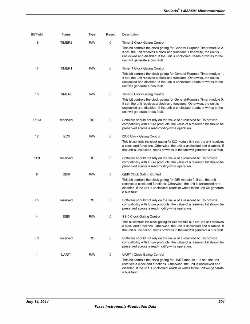
DescriptionResetTypeNameBit/Field
Timer 2 Clock Gating ControlThis bit controls the clock gating for General-Purpose Timer module 2.If set, the unit receives a clock and functions. Otherwise, the unit isunclocked and disabled. If the unit is unclocked, reads or writes to theunit will generate a bus fault.
0R/WTIMER218
Timer 1 Clock Gating ControlThis bit controls the clock gating for General-Purpose Timer module 1.If set, the unit receives a clock and functions. Otherwise, the unit isunclocked and disabled. If the unit is unclocked, reads or writes to theunit will generate a bus fault.
0R/WTIMER117
Timer 0 Clock Gating ControlThis bit controls the clock gating for General-Purpose Timer module 0.If set, the unit receives a clock and functions. Otherwise, the unit isunclocked and disabled. If the unit is unclocked, reads or writes to theunit will generate a bus fault.
0R/WTIMER016
Software should not rely on the value of a reserved bit. To providecompatibility with future products, the value of a reserved bit should bepreserved across a read-modify-write operation.
0ROreserved15:13
I2C0 Clock Gating ControlThis bit controls the clock gating for I2Cmodule 0. If set, the unit receivesa clock and functions. Otherwise, the unit is unclocked and disabled. Ifthe unit is unclocked, reads or writes to the unit will generate a bus fault.
0R/WI2C012
Software should not rely on the value of a reserved bit. To providecompatibility with future products, the value of a reserved bit should bepreserved across a read-modify-write operation.
0ROreserved11:9
QEI0 Clock Gating ControlThis bit controls the clock gating for QEI module 0. If set, the unitreceives a clock and functions. Otherwise, the unit is unclocked anddisabled. If the unit is unclocked, reads or writes to the unit will generatea bus fault.
0R/WQEI08
Software should not rely on the value of a reserved bit. To providecompatibility with future products, the value of a reserved bit should bepreserved across a read-modify-write operation.
0ROreserved7:5
SSI0 Clock Gating ControlThis bit controls the clock gating for SSI module 0. If set, the unit receivesa clock and functions. Otherwise, the unit is unclocked and disabled. Ifthe unit is unclocked, reads or writes to the unit will generate a bus fault.
0R/WSSI04
Software should not rely on the value of a reserved bit. To providecompatibility with future products, the value of a reserved bit should bepreserved across a read-modify-write operation.
0ROreserved3:2
UART1 Clock Gating ControlThis bit controls the clock gating for UART module 1. If set, the unitreceives a clock and functions. Otherwise, the unit is unclocked anddisabled. If the unit is unclocked, reads or writes to the unit will generatea bus fault.
0R/WUART11
201July 14, 2014Texas Instruments-Production Data
Stellaris® LM3S601 Microcontroller

DescriptionResetTypeNameBit/Field
UART0 Clock Gating ControlThis bit controls the clock gating for UART module 0. If set, the unitreceives a clock and functions. Otherwise, the unit is unclocked anddisabled. If the unit is unclocked, reads or writes to the unit will generatea bus fault.
0R/WUART00
July 14, 2014202Texas Instruments-Production Data
System Control
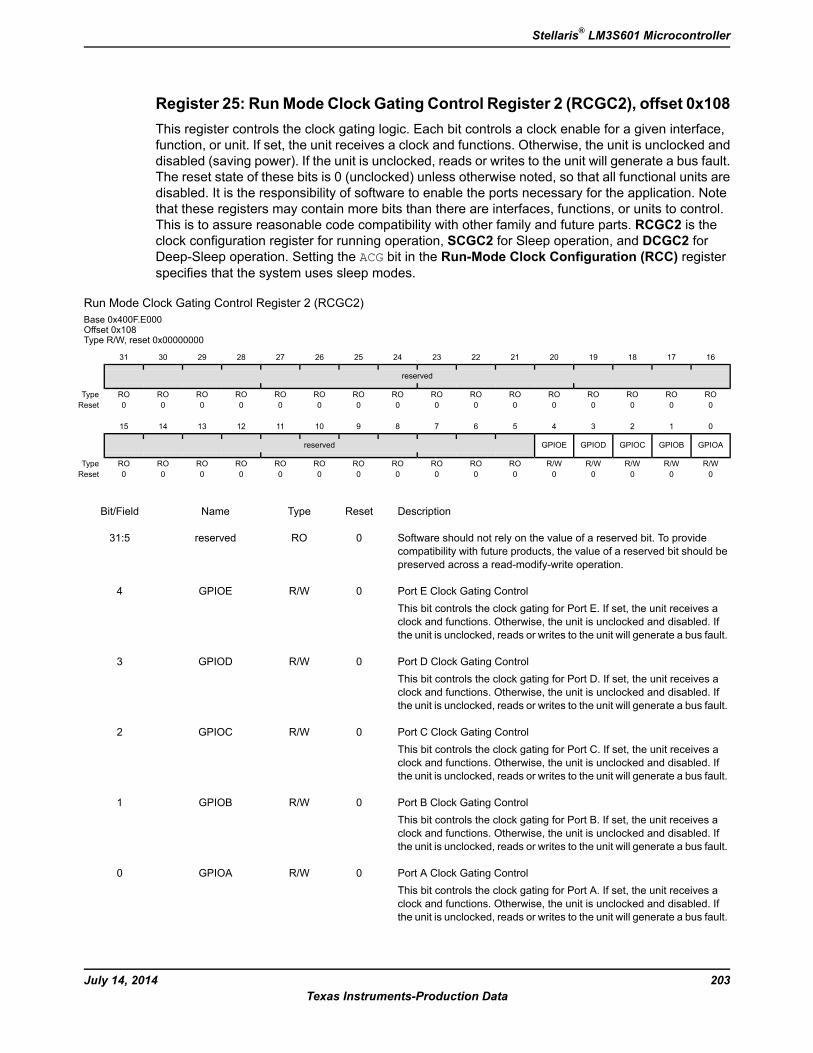
Register 25: RunMode Clock Gating Control Register 2 (RCGC2), offset 0x108This register controls the clock gating logic. Each bit controls a clock enable for a given interface,function, or unit. If set, the unit receives a clock and functions. Otherwise, the unit is unclocked anddisabled (saving power). If the unit is unclocked, reads or writes to the unit will generate a bus fault.The reset state of these bits is 0 (unclocked) unless otherwise noted, so that all functional units aredisabled. It is the responsibility of software to enable the ports necessary for the application. Notethat these registers may contain more bits than there are interfaces, functions, or units to control.This is to assure reasonable code compatibility with other family and future parts. RCGC2 is theclock configuration register for running operation, SCGC2 for Sleep operation, and DCGC2 forDeep-Sleep operation. Setting the ACG bit in the Run-Mode Clock Configuration (RCC) registerspecifies that the system uses sleep modes.
Run Mode Clock Gating Control Register 2 (RCGC2)Base 0x400F.E000Offset 0x108Type R/W, reset 0x00000000
16171819202122232425262728293031
reserved
ROROROROROROROROROROROROROROROROType0000000000000000Reset
0123456789101112131415
GPIOAGPIOBGPIOCGPIODGPIOEreserved
R/WR/WR/WR/WR/WROROROROROROROROROROROType0000000000000000Reset
DescriptionResetTypeNameBit/Field
Software should not rely on the value of a reserved bit. To providecompatibility with future products, the value of a reserved bit should bepreserved across a read-modify-write operation.
0ROreserved31:5
Port E Clock Gating ControlThis bit controls the clock gating for Port E. If set, the unit receives aclock and functions. Otherwise, the unit is unclocked and disabled. Ifthe unit is unclocked, reads or writes to the unit will generate a bus fault.
0R/WGPIOE4
Port D Clock Gating ControlThis bit controls the clock gating for Port D. If set, the unit receives aclock and functions. Otherwise, the unit is unclocked and disabled. Ifthe unit is unclocked, reads or writes to the unit will generate a bus fault.
0R/WGPIOD3
Port C Clock Gating ControlThis bit controls the clock gating for Port C. If set, the unit receives aclock and functions. Otherwise, the unit is unclocked and disabled. Ifthe unit is unclocked, reads or writes to the unit will generate a bus fault.
0R/WGPIOC2
Port B Clock Gating ControlThis bit controls the clock gating for Port B. If set, the unit receives aclock and functions. Otherwise, the unit is unclocked and disabled. Ifthe unit is unclocked, reads or writes to the unit will generate a bus fault.
0R/WGPIOB1
Port A Clock Gating ControlThis bit controls the clock gating for Port A. If set, the unit receives aclock and functions. Otherwise, the unit is unclocked and disabled. Ifthe unit is unclocked, reads or writes to the unit will generate a bus fault.
0R/WGPIOA0
203July 14, 2014Texas Instruments-Production Data
Stellaris® LM3S601 Microcontroller

Register 26: Sleep Mode Clock Gating Control Register 2 (SCGC2), offset0x118This register controls the clock gating logic. Each bit controls a clock enable for a given interface,function, or unit. If set, the unit receives a clock and functions. Otherwise, the unit is unclocked anddisabled (saving power). If the unit is unclocked, reads or writes to the unit will generate a bus fault.The reset state of these bits is 0 (unclocked) unless otherwise noted, so that all functional units aredisabled. It is the responsibility of software to enable the ports necessary for the application. Notethat these registers may contain more bits than there are interfaces, functions, or units to control.This is to assure reasonable code compatibility with other family and future parts. RCGC2 is theclock configuration register for running operation, SCGC2 for Sleep operation, and DCGC2 forDeep-Sleep operation. Setting the ACG bit in the Run-Mode Clock Configuration (RCC) registerspecifies that the system uses sleep modes.
Sleep Mode Clock Gating Control Register 2 (SCGC2)Base 0x400F.E000Offset 0x118Type R/W, reset 0x00000000
16171819202122232425262728293031
reserved
ROROROROROROROROROROROROROROROROType0000000000000000Reset
0123456789101112131415
GPIOAGPIOBGPIOCGPIODGPIOEreserved
R/WR/WR/WR/WR/WROROROROROROROROROROROType0000000000000000Reset
DescriptionResetTypeNameBit/Field
Software should not rely on the value of a reserved bit. To providecompatibility with future products, the value of a reserved bit should bepreserved across a read-modify-write operation.
0ROreserved31:5
Port E Clock Gating ControlThis bit controls the clock gating for Port E. If set, the unit receives aclock and functions. Otherwise, the unit is unclocked and disabled. Ifthe unit is unclocked, reads or writes to the unit will generate a bus fault.
0R/WGPIOE4
Port D Clock Gating ControlThis bit controls the clock gating for Port D. If set, the unit receives aclock and functions. Otherwise, the unit is unclocked and disabled. Ifthe unit is unclocked, reads or writes to the unit will generate a bus fault.
0R/WGPIOD3
Port C Clock Gating ControlThis bit controls the clock gating for Port C. If set, the unit receives aclock and functions. Otherwise, the unit is unclocked and disabled. Ifthe unit is unclocked, reads or writes to the unit will generate a bus fault.
0R/WGPIOC2
Port B Clock Gating ControlThis bit controls the clock gating for Port B. If set, the unit receives aclock and functions. Otherwise, the unit is unclocked and disabled. Ifthe unit is unclocked, reads or writes to the unit will generate a bus fault.
0R/WGPIOB1
July 14, 2014204Texas Instruments-Production Data
System Control
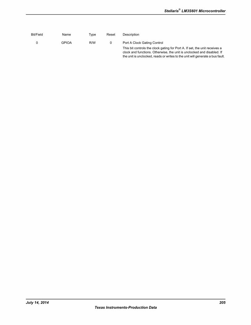
DescriptionResetTypeNameBit/Field
Port A Clock Gating ControlThis bit controls the clock gating for Port A. If set, the unit receives aclock and functions. Otherwise, the unit is unclocked and disabled. Ifthe unit is unclocked, reads or writes to the unit will generate a bus fault.
0R/WGPIOA0
205July 14, 2014Texas Instruments-Production Data
Stellaris® LM3S601 Microcontroller
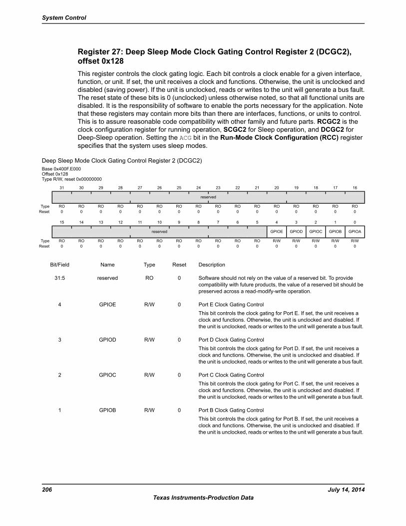
Register 27: Deep Sleep Mode Clock Gating Control Register 2 (DCGC2),offset 0x128This register controls the clock gating logic. Each bit controls a clock enable for a given interface,function, or unit. If set, the unit receives a clock and functions. Otherwise, the unit is unclocked anddisabled (saving power). If the unit is unclocked, reads or writes to the unit will generate a bus fault.The reset state of these bits is 0 (unclocked) unless otherwise noted, so that all functional units aredisabled. It is the responsibility of software to enable the ports necessary for the application. Notethat these registers may contain more bits than there are interfaces, functions, or units to control.This is to assure reasonable code compatibility with other family and future parts. RCGC2 is theclock configuration register for running operation, SCGC2 for Sleep operation, and DCGC2 forDeep-Sleep operation. Setting the ACG bit in the Run-Mode Clock Configuration (RCC) registerspecifies that the system uses sleep modes.
Deep Sleep Mode Clock Gating Control Register 2 (DCGC2)Base 0x400F.E000Offset 0x128Type R/W, reset 0x00000000
16171819202122232425262728293031
reserved
ROROROROROROROROROROROROROROROROType0000000000000000Reset
0123456789101112131415
GPIOAGPIOBGPIOCGPIODGPIOEreserved
R/WR/WR/WR/WR/WROROROROROROROROROROROType0000000000000000Reset
DescriptionResetTypeNameBit/Field
Software should not rely on the value of a reserved bit. To providecompatibility with future products, the value of a reserved bit should bepreserved across a read-modify-write operation.
0ROreserved31:5
Port E Clock Gating ControlThis bit controls the clock gating for Port E. If set, the unit receives aclock and functions. Otherwise, the unit is unclocked and disabled. Ifthe unit is unclocked, reads or writes to the unit will generate a bus fault.
0R/WGPIOE4
Port D Clock Gating ControlThis bit controls the clock gating for Port D. If set, the unit receives aclock and functions. Otherwise, the unit is unclocked and disabled. Ifthe unit is unclocked, reads or writes to the unit will generate a bus fault.
0R/WGPIOD3
Port C Clock Gating ControlThis bit controls the clock gating for Port C. If set, the unit receives aclock and functions. Otherwise, the unit is unclocked and disabled. Ifthe unit is unclocked, reads or writes to the unit will generate a bus fault.
0R/WGPIOC2
Port B Clock Gating ControlThis bit controls the clock gating for Port B. If set, the unit receives aclock and functions. Otherwise, the unit is unclocked and disabled. Ifthe unit is unclocked, reads or writes to the unit will generate a bus fault.
0R/WGPIOB1
July 14, 2014206Texas Instruments-Production Data
System Control

DescriptionResetTypeNameBit/Field
Port A Clock Gating ControlThis bit controls the clock gating for Port A. If set, the unit receives aclock and functions. Otherwise, the unit is unclocked and disabled. Ifthe unit is unclocked, reads or writes to the unit will generate a bus fault.
0R/WGPIOA0
207July 14, 2014Texas Instruments-Production Data
Stellaris® LM3S601 Microcontroller
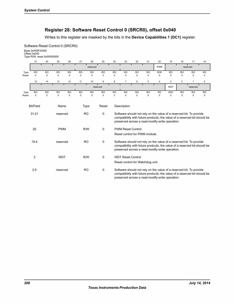
Register 28: Software Reset Control 0 (SRCR0), offset 0x040Writes to this register are masked by the bits in the Device Capabilities 1 (DC1) register.
Software Reset Control 0 (SRCR0)Base 0x400F.E000Offset 0x040Type R/W, reset 0x00000000
16171819202122232425262728293031
reservedPWMreserved
ROROROROR/WROROROROROROROROROROROType0000000000000000Reset
0123456789101112131415
reservedWDTreserved
ROROROR/WROROROROROROROROROROROROType0000000000000000Reset
DescriptionResetTypeNameBit/Field
Software should not rely on the value of a reserved bit. To providecompatibility with future products, the value of a reserved bit should bepreserved across a read-modify-write operation.
0ROreserved31:21
PWM Reset ControlReset control for PWM module.
0R/WPWM20
Software should not rely on the value of a reserved bit. To providecompatibility with future products, the value of a reserved bit should bepreserved across a read-modify-write operation.
0ROreserved19:4
WDT Reset ControlReset control for Watchdog unit.
0R/WWDT3
Software should not rely on the value of a reserved bit. To providecompatibility with future products, the value of a reserved bit should bepreserved across a read-modify-write operation.
0ROreserved2:0
July 14, 2014208Texas Instruments-Production Data
System Control
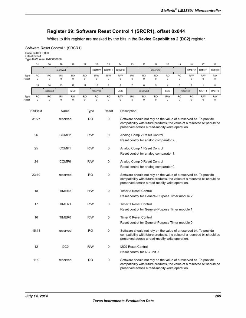
Register 29: Software Reset Control 1 (SRCR1), offset 0x044Writes to this register are masked by the bits in the Device Capabilities 2 (DC2) register.
Software Reset Control 1 (SRCR1)Base 0x400F.E000Offset 0x044Type R/W, reset 0x00000000
16171819202122232425262728293031
TIMER0TIMER1TIMER2reservedCOMP0COMP1COMP2reserved
R/WR/WR/WROROROROROR/WR/WR/WROROROROROType0000000000000000Reset
0123456789101112131415
UART0UART1reservedSSI0reservedQEI0reservedI2C0reserved
R/WR/WROROR/WROROROR/WROROROR/WROROROType0000000000000000Reset
DescriptionResetTypeNameBit/Field
Software should not rely on the value of a reserved bit. To providecompatibility with future products, the value of a reserved bit should bepreserved across a read-modify-write operation.
0ROreserved31:27
Analog Comp 2 Reset ControlReset control for analog comparator 2.
0R/WCOMP226
Analog Comp 1 Reset ControlReset control for analog comparator 1.
0R/WCOMP125
Analog Comp 0 Reset ControlReset control for analog comparator 0.
0R/WCOMP024
Software should not rely on the value of a reserved bit. To providecompatibility with future products, the value of a reserved bit should bepreserved across a read-modify-write operation.
0ROreserved23:19
Timer 2 Reset ControlReset control for General-Purpose Timer module 2.
0R/WTIMER218
Timer 1 Reset ControlReset control for General-Purpose Timer module 1.
0R/WTIMER117
Timer 0 Reset ControlReset control for General-Purpose Timer module 0.
0R/WTIMER016
Software should not rely on the value of a reserved bit. To providecompatibility with future products, the value of a reserved bit should bepreserved across a read-modify-write operation.
0ROreserved15:13
I2C0 Reset ControlReset control for I2C unit 0.
0R/WI2C012
Software should not rely on the value of a reserved bit. To providecompatibility with future products, the value of a reserved bit should bepreserved across a read-modify-write operation.
0ROreserved11:9
209July 14, 2014Texas Instruments-Production Data
Stellaris® LM3S601 Microcontroller
DescriptionResetTypeNameBit/Field
QEI0 Reset ControlReset control for QEI unit 0.
0R/WQEI08
Software should not rely on the value of a reserved bit. To providecompatibility with future products, the value of a reserved bit should bepreserved across a read-modify-write operation.
0ROreserved7:5
SSI0 Reset ControlReset control for SSI unit 0.
0R/WSSI04
Software should not rely on the value of a reserved bit. To providecompatibility with future products, the value of a reserved bit should bepreserved across a read-modify-write operation.
0ROreserved3:2
UART1 Reset ControlReset control for UART unit 1.
0R/WUART11
UART0 Reset ControlReset control for UART unit 0.
0R/WUART00
July 14, 2014210Texas Instruments-Production Data
System Control
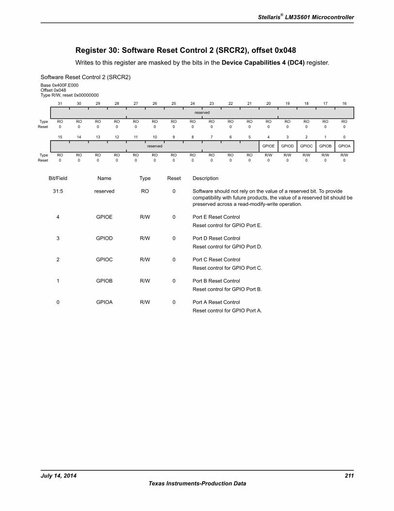
Register 30: Software Reset Control 2 (SRCR2), offset 0x048Writes to this register are masked by the bits in the Device Capabilities 4 (DC4) register.
Software Reset Control 2 (SRCR2)Base 0x400F.E000Offset 0x048Type R/W, reset 0x00000000
16171819202122232425262728293031
reserved
ROROROROROROROROROROROROROROROROType0000000000000000Reset
0123456789101112131415
GPIOAGPIOBGPIOCGPIODGPIOEreserved
R/WR/WR/WR/WR/WROROROROROROROROROROROType0000000000000000Reset
DescriptionResetTypeNameBit/Field
Software should not rely on the value of a reserved bit. To providecompatibility with future products, the value of a reserved bit should bepreserved across a read-modify-write operation.
0ROreserved31:5
Port E Reset ControlReset control for GPIO Port E.
0R/WGPIOE4
Port D Reset ControlReset control for GPIO Port D.
0R/WGPIOD3
Port C Reset ControlReset control for GPIO Port C.
0R/WGPIOC2
Port B Reset ControlReset control for GPIO Port B.
0R/WGPIOB1
Port A Reset ControlReset control for GPIO Port A.
0R/WGPIOA0
211July 14, 2014Texas Instruments-Production Data
Stellaris® LM3S601 Microcontroller
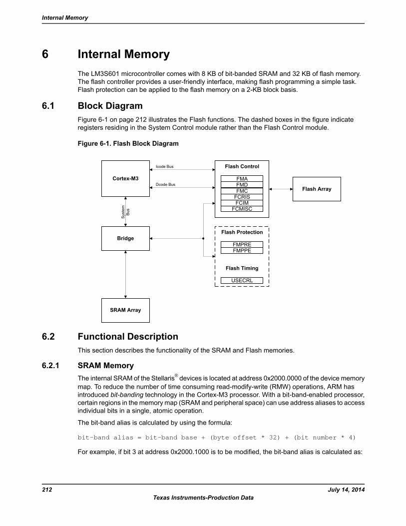
6 Internal MemoryThe LM3S601 microcontroller comes with 8 KB of bit-banded SRAM and 32 KB of flash memory.The flash controller provides a user-friendly interface, making flash programming a simple task.Flash protection can be applied to the flash memory on a 2-KB block basis.
6.1 Block DiagramFigure 6-1 on page 212 illustrates the Flash functions. The dashed boxes in the figure indicateregisters residing in the System Control module rather than the Flash Control module.
Figure 6-1. Flash Block Diagram
Flash Control
FMAFMD
FCIMFCMISC
Flash Array
Cortex-M3
Bridge
SRAM Array
System
Bus
Icode Bus
Dcode Bus
Flash Protection
FMPREFMPPE
Flash Timing
USECRL
FMCFCRIS
6.2 Functional DescriptionThis section describes the functionality of the SRAM and Flash memories.
6.2.1 SRAM MemoryThe internal SRAM of the Stellaris® devices is located at address 0x2000.0000 of the device memorymap. To reduce the number of time consuming read-modify-write (RMW) operations, ARM hasintroduced bit-banding technology in the Cortex-M3 processor. With a bit-band-enabled processor,certain regions in thememory map (SRAM and peripheral space) can use address aliases to accessindividual bits in a single, atomic operation.
The bit-band alias is calculated by using the formula:
bit-band alias = bit-band base + (byte offset * 32) + (bit number * 4)
For example, if bit 3 at address 0x2000.1000 is to be modified, the bit-band alias is calculated as:
July 14, 2014212Texas Instruments-Production Data
Internal Memory
0x2200.0000 + (0x1000 * 32) + (3 * 4) = 0x2202.000C
With the alias address calculated, an instruction performing a read/write to address 0x2202.000Callows direct access to only bit 3 of the byte at address 0x2000.1000.
For details about bit-banding, see “Bit-Banding” on page 66.
6.2.2 Flash MemoryThe flash is organized as a set of 1-KB blocks that can be individually erased. Erasing a blockcauses the entire contents of the block to be reset to all 1s. An individual 32-bit word can beprogrammed to change bits that are currently 1 to a 0. These blocks are paired into a set of 2-KBblocks that can be individually protected. The protection allows blocks to be marked as read-onlyor execute-only, providing different levels of code protection. Read-only blocks cannot be erasedor programmed, protecting the contents of those blocks from being modified. Execute-only blockscannot be erased or programmed, and can only be read by the controller instruction fetch mechanism,protecting the contents of those blocks from being read by either the controller or by a debugger.
See also “Serial Flash Loader” on page 537 for a preprogrammed flash-resident utility used todownload code to the flash memory of a device without the use of a debug interface.
6.2.2.1 Flash Memory TimingThe timing for the flash is automatically handled by the flash controller. However, in order to do so,it must know the clock rate of the system in order to time its internal signals properly. The numberof clock cycles per microsecond must be provided to the flash controller for it to accomplish thistiming. It is software's responsibility to keep the flash controller updated with this information via theUSec Reload (USECRL) register.
On reset, theUSECRL register is loaded with a value that configures the flash timing so that it workswith the maximum clock rate of the part. If software changes the system operating frequency, thenew operating frequency minus 1 (in MHz) must be loaded into USECRL before any flashmodifications are attempted. For example, if the device is operating at a speed of 20 MHz, a valueof 0x13 (20-1) must be written to the USECRL register.
6.2.2.2 Flash Memory ProtectionThe user is provided two forms of flash protection per 2-KB flash blocks in two 32-bit wideregisters.The protection policy for each form is controlled by individual bits (per policy per block) inthe FMPPEn and FMPREn registers.
Flash Memory Protection Program Enable (FMPPEn): If set, the block may be programmed(written) or erased. If cleared, the block may not be changed.
Flash Memory Protection Read Enable (FMPREn): If a bit is set, the corresponding block maybe executed or read by software or debuggers. If a bit is cleared, the corresponding block mayonly be executed, and contents of the memory block are prohibited from being read as data.
The policies may be combined as shown in Table 6-1 on page 213.
Table 6-1. Flash Protection Policy Combinations
ProtectionFMPREnFMPPEn
Execute-only protection. The block may only be executed and may not be written or erased.This mode is used to protect code.
00
213July 14, 2014Texas Instruments-Production Data
Stellaris® LM3S601 Microcontroller
Table 6-1. Flash Protection Policy Combinations (continued)
ProtectionFMPREnFMPPEn
The block may be written, erased or executed, but not read. This combination is unlikely tobe used.
01
Read-only protection. The block may be read or executed but may not be written or erased.This mode is used to lock the block from further modification while allowing any read orexecute access.
10
No protection. The block may be written, erased, executed or read.11
A Flashmemory access that attempts to read a read-protected block (FMPREn bit is set) is prohibitedand generates a bus fault. A Flash memory access that attempts to program or erase aprogram-protected block (FMPPEn bit is set) is prohibited and can optionally generate an interrupt(by setting the AMASK bit in the Flash Controller Interrupt Mask (FCIM) register) to alert softwaredevelopers of poorly behaving software during the development and debug phases.
The factory settings for the FMPREn and FMPPEn registers are a value of 1 for all implementedbanks. These settings create a policy of open access and programmability. The register bits maybe changed by clearing the specific register bit. The changes are not permanent until the registeris committed (saved), at which point the bit change is permanent. If a bit is changed from a 1 to a0 and not committed, it may be restored by executing a power-on reset sequence. The changesare committed using the Flash Memory Control (FMC) register.
6.2.2.3 Execute-Only ProtectionExecute-only protection prevents both modification and visibility to a protected flash block. Thismode is intended to be used in situations where a device requires debug capability, yet portions ofthe application space must be protected from external access. An example of this is a companywho wishes to sell Stellaris devices with their proprietary software pre-programmed, yet allow theend user to add custom code to an unprotected region of the flash (such as a motor control modulewith a customizable motor configuration section in flash).
Literal data introduces a complication to the protection mechanism. When C code is compiled andlinked, literal data (constants, and so on) is typically placed in the text section, between functions,by the compiler. The literal data is accessed at run time through the use of the LDR instruction,which loads the data from memory using a PC-relative memory address. The execution of the LDRinstruction generates a read transaction across the Cortex-M3's DCode bus, which is subject to theexecute-only protection mechanism. If the accessed block is marked as execute only, the transactionis blocked, and the processor is prevented from loading the constant data and, therefore, inhibitingcorrect execution. Therefore, using execute-only protection requires that literal data be handleddifferently. There are three ways to address this:
1. Use a compiler that allows literal data to be collected into a separate section that is put into oneor more read-enabled flash blocks. Note that the LDR instruction may use a PC-relativeaddress–-in which case the literal pool cannot be located outside the span of the offset–-or thesoftware may reserve a register to point to the base address of the literal pool and the LDRoffset is relative to the beginning of the pool.
2. Use a compiler that generates literal data from arithmetic instruction immediate data andsubsequent computation.
3. Use method 1 or 2, but in assembly language, if the compiler does not support either method.
July 14, 2014214Texas Instruments-Production Data
Internal Memory
6.2.2.4 Read-Only ProtectionRead-only protection prevents the contents of the flash block from being re-programmed, while stillallowing the content to be read by processor or the debug interface. Note that if a FMPREn bit iscleared, all read accesses to the Flash memory block are disallowed, including any data accesses.Care must be taken not to store required data in a Flash memory block that has the associatedFMPREn bit cleared.
The read-only mode does not prevent read access to the stored program, but it does provideprotection against accidental (or malicious) erasure or programming. Read-only is especially usefulfor utilities like the boot loader when the debug interface is permanently disabled. In suchcombinations, the boot loader, which provides access control to the Flash memory, is protectedfrom being erased or modified.
6.2.2.5 Permanently Disabling DebugFor extremely sensitive applications, the debug interface to the processor and peripherals can bepermanently disabled, blocking all accesses to the device through the JTAG or SWD interfaces.With the debug interface disabled, it is still possible to perform standard IEEE instructions (such asboundary scan operations), but access to the processor and peripherals is blocked.
The two most-significant bits of the FMPRE register are the DBG bits, and control whether or not thedebug interface is turned on or off. Since the DBG bits are part of the FMPRE register, the user losesthe capability to mark the upper two flash blocks in a 64 KB flash device as execute-only.
The debug interface should not be permanently disabled without providing some mechanism–-suchas the boot loader–-to provide customer-installable updates or bug fixes. Disabling the debuginterface is permanent and cannot be reversed.
6.2.2.6 InterruptsThe Flash memory controller can generate interrupts when the following conditions are observed:
Programming Interrupt - signals when a program or erase action is complete.
Access Interrupt - signals when a program or erase action has been attempted on a 2-kB blockof memory that is protected by its corresponding FMPPEn bit.
The interrupt events that can trigger a controller-level interrupt are defined in the Flash ControllerMasked Interrupt Status (FCMIS) register (see page 224) by setting the corresponding MASK bits.If interrupts are not used, the raw interrupt status is always visible via the Flash Controller RawInterrupt Status (FCRIS) register (see page 223).
Interrupts are always cleared (for both the FCMIS and FCRIS registers) by writing a 1 to thecorresponding bit in the Flash Controller Masked Interrupt Status and Clear (FCMISC) register(see page 225).
6.2.2.7 Flash Memory Protection by Disabling Debug AccessFlash memory may also be protected by permanently disabling access to the Debug Access Port(DAP) through the JTAG and SWD interfaces. Access is disabled by clearing the DBG field of theFMPRE register.
If the DBG field in the Flash Memory Protection Read Enable (FMPRE) register is programmedto 0x2, access to the DAP is enabled through the JTAG and SWD interfaces. If clear, access to theDAP is disabled. The DBG field programming becomes permanent and irreversible after a commitsequence is performed.
215July 14, 2014Texas Instruments-Production Data
Stellaris® LM3S601 Microcontroller
In the initial state provided from the factory, access is enabled in order to facilitate code developmentand debug. Access to the DAP may be disabled at the end of the manufacturing flow, once all testshave passed and software has been loaded. This change does not take effect until the next power-upof the device. Note that it is recommended that disabling access to the DAP be combined with amechanism for providing end-user installable updates (if necessary) such as the Stellaris boot loader.
Important: Once the DBG field is cleared and committed, this field can never be restored to thefactory-programmed value—whichmeans the JTAG/SWD interface to the debugmodulecan never be re-enabled. This sequence does NOT disable the JTAG controller, it onlydisables the access of the DAP through the JTAG or SWD interfaces. The JTAG interfaceremains functional and access to the Test Access Port remains enabled, allowing theuser to execute the IEEE JTAG-defined instructions (for example, to perform boundaryscan operations).
When using the FMPRE bits to protect Flash memory from being read as data (to mark sets of 2-KBblocks of Flash memory as execute-only), these one-time-programmable bits should be written atthe same time that the debug disable bits are programmed. Mechanisms to execute the one-timecode sequence to disable all debug access include:
Selecting the debug disable option in the Stellaris boot loader
Loading the debug disable sequence into SRAM and running it once from SRAM afterprogramming the final end application code into Flash memory
6.3 Flash Memory Initialization and ConfigurationThis section shows examples for using the flash controller to perform various operations on thecontents of the flash memory.
6.3.1 Changing Flash Protection BitsAs discussed in “Flash Memory Protection” on page 213, changes to the protection bits must becommitted before they take effect. The sequence below is used change and commit a block protectionbit in the FMPRE or FMPPE registers. The sequence to change and commit a bit in software is asfollows:
1. The FlashMemory ProtectionReadEnable (FMPRE) and FlashMemory Protection ProgramEnable (FMPPE) registers are written, changing the intended bit(s). The action of these changescan be tested by software while in this state.
2. The FlashMemory Address (FMA) register (see page 219) bit 0 is set to 1 if the FMPPE registeris to be committed; otherwise, a 0 commits the FMPRE register.
3. The Flash Memory Control (FMC) register (see page 221) is written with the COMT bit set. Thisinitiates a write sequence and commits the changes.
There is a special sequence to change and commit the DBG bits in the Flash Memory ProtectionRead Enable (FMPRE) register. This sequence also sets and commits any changes from 1 to 0 inthe block protection bits (for execute-only) in the FMPRE register.
1. The FlashMemory Protection Read Enable (FMPRE) register is written, changing the intendedbit(s). The action of these changes can be tested by software while in this state.
2. The Flash Memory Address (FMA) register (see page 219) is written with a value of 0x900.
July 14, 2014216Texas Instruments-Production Data
Internal Memory
3. The Flash Memory Control (FMC) register (see page 221) is written with the COMT bit set. Thisinitiates a write sequence and commits the changes.
Below is an example code sequence to permanently disable the JTAG and SWD interface to thedebug module using DriverLib:
#include "hw_types.h"#include "hw_flash.h"voidpermanently_disable_jtag_swd(void) // // Clear the DBG field of the FMPRE register. Note that the value // used in this instance does not affect the state of the BlockN // bits, but were the value different, all bits in the FMPRE are // affected by this function! // HWREG(FLASH_FMPRE) &= 0x3fffffff; // // The following sequence activates the one-time // programming of the FMPRE register. // HWREG(FLASH_FMA) = 0x900; HWREG(FLASH_FMC) = (FLASH_FMC_WRKEY | FLASH_FMC_COMT); // // Wait until the operation is complete. // while (HWREG(FLASH_FMC) & FLASH_FMC_COMT)
6.3.2 Flash ProgrammingThe Stellaris devices provide a user-friendly interface for flash programming. All erase/programoperations are handled via three registers: FMA, FMD, and FMC.
During a Flash memory operation (write, page erase, or mass erase) access to the Flash memoryis inhibited. As a result, instruction and literal fetches are held off until the Flash memory operationis complete. If instruction execution is required during a Flash memory operation, the code that isexecuting must be placed in SRAM and executed from there while the flash operation is in progress.
6.3.2.1 To program a 32-bit word
1. Write source data to the FMD register.
2. Write the target address to the FMA register.
3. Write the flash write key and the WRITE bit (a value of 0xA442.0001) to the FMC register.
4. Poll the FMC register until the WRITE bit is cleared.
6.3.2.2 To perform an erase of a 1-KB page
1. Write the page address to the FMA register.
217July 14, 2014Texas Instruments-Production Data
Stellaris® LM3S601 Microcontroller
2. Write the flash write key and the ERASE bit (a value of 0xA442.0002) to the FMC register.
3. Poll the FMC register until the ERASE bit is cleared.
6.3.2.3 To perform a mass erase of the flash
1. Write the flash write key and the MERASE bit (a value of 0xA442.0004) to the FMC register.
2. Poll the FMC register until the MERASE bit is cleared.
6.4 Register MapTable 6-2 on page 218 lists the Flash memory and control registers. The offset listed is a hexadecimalincrement to the register's address. The FMA, FMD, FMC, FCRIS, FCIM, and FCMISC registeroffsets are relative to the Flash memory control base address of 0x400F.D000. The Flash memoryprotection register offsets are relative to the System Control base address of 0x400F.E000.
Table 6-2. Flash Register Map
SeepageDescriptionResetTypeNameOffset
Flash Memory Control Registers (Flash Control Offset)
219Flash Memory Address0x0000.0000R/WFMA0x000
220Flash Memory Data0x0000.0000R/WFMD0x004
221Flash Memory Control0x0000.0000R/WFMC0x008
223Flash Controller Raw Interrupt Status0x0000.0000ROFCRIS0x00C
224Flash Controller Interrupt Mask0x0000.0000R/WFCIM0x010
225Flash Controller Masked Interrupt Status and Clear0x0000.0000R/W1CFCMISC0x014
Flash Memory Protection Registers (System Control Offset)
228Flash Memory Protection Read Enable0x8000.FFFFR/WFMPRE0x130
229Flash Memory Protection Program Enable0x0000.FFFFR/WFMPPE0x134
227USec Reload0x31R/WUSECRL0x140
6.5 Flash Register Descriptions (Flash Control Offset)This section lists and describes the Flash Memory registers, in numerical order by address offset.Registers in this section are relative to the Flash control base address of 0x400F.D000.
July 14, 2014218Texas Instruments-Production Data
Internal Memory
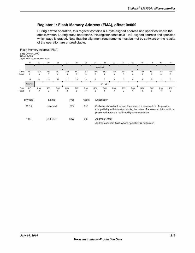
Register 1: Flash Memory Address (FMA), offset 0x000During a write operation, this register contains a 4-byte-aligned address and specifies where thedata is written. During erase operations, this register contains a 1 KB-aligned address and specifieswhich page is erased. Note that the alignment requirements must be met by software or the resultsof the operation are unpredictable.
Flash Memory Address (FMA)Base 0x400F.D000Offset 0x000Type R/W, reset 0x0000.0000
16171819202122232425262728293031
reserved
ROROROROROROROROROROROROROROROROType0000000000000000Reset
0123456789101112131415
OFFSETreserved
R/WR/WR/WR/WR/WR/WR/WR/WR/WR/WR/WR/WR/WR/WR/WROType0000000000000000Reset
DescriptionResetTypeNameBit/Field
Software should not rely on the value of a reserved bit. To providecompatibility with future products, the value of a reserved bit should bepreserved across a read-modify-write operation.
0x0ROreserved31:15
Address OffsetAddress offset in flash where operation is performed.
0x0R/WOFFSET14:0
219July 14, 2014Texas Instruments-Production Data
Stellaris® LM3S601 Microcontroller
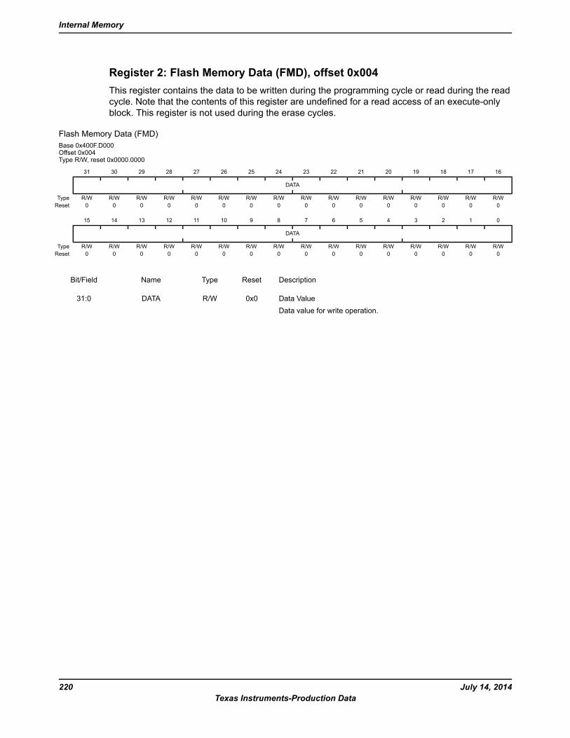
Register 2: Flash Memory Data (FMD), offset 0x004This register contains the data to be written during the programming cycle or read during the readcycle. Note that the contents of this register are undefined for a read access of an execute-onlyblock. This register is not used during the erase cycles.
Flash Memory Data (FMD)Base 0x400F.D000Offset 0x004Type R/W, reset 0x0000.0000
16171819202122232425262728293031
DATA
R/WR/WR/WR/WR/WR/WR/WR/WR/WR/WR/WR/WR/WR/WR/WR/WType0000000000000000Reset
0123456789101112131415
DATA
R/WR/WR/WR/WR/WR/WR/WR/WR/WR/WR/WR/WR/WR/WR/WR/WType0000000000000000Reset
DescriptionResetTypeNameBit/Field
Data ValueData value for write operation.
0x0R/WDATA31:0
July 14, 2014220Texas Instruments-Production Data
Internal Memory
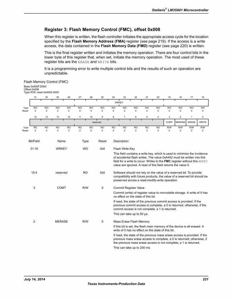
Register 3: Flash Memory Control (FMC), offset 0x008When this register is written, the flash controller initiates the appropriate access cycle for the locationspecified by the Flash Memory Address (FMA) register (see page 219). If the access is a writeaccess, the data contained in the Flash Memory Data (FMD) register (see page 220) is written.
This is the final register written and initiates the memory operation. There are four control bits in thelower byte of this register that, when set, initiate the memory operation. The most used of theseregister bits are the ERASE and WRITE bits.
It is a programming error to write multiple control bits and the results of such an operation areunpredictable.
Flash Memory Control (FMC)Base 0x400F.D000Offset 0x008Type R/W, reset 0x0000.0000
16171819202122232425262728293031
WRKEY
WOWOWOWOWOWOWOWOWOWOWOWOWOWOWOWOType0000000000000000Reset
0123456789101112131415
WRITEERASEMERASECOMTreserved
R/WR/WR/WR/WROROROROROROROROROROROROType0000000000000000Reset
DescriptionResetTypeNameBit/Field
Flash Write KeyThis field contains a write key, which is used to minimize the incidenceof accidental flash writes. The value 0xA442 must be written into thisfield for a write to occur. Writes to the FMC register without this WRKEYvalue are ignored. A read of this field returns the value 0.
0x0WOWRKEY31:16
Software should not rely on the value of a reserved bit. To providecompatibility with future products, the value of a reserved bit should bepreserved across a read-modify-write operation.
0x0ROreserved15:4
Commit Register ValueCommit (write) of register value to nonvolatile storage. A write of 0 hasno effect on the state of this bit.If read, the state of the previous commit access is provided. If theprevious commit access is complete, a 0 is returned; otherwise, if thecommit access is not complete, a 1 is returned.This can take up to 50 μs.
0R/WCOMT3
Mass Erase Flash MemoryIf this bit is set, the flash main memory of the device is all erased. Awrite of 0 has no effect on the state of this bit.If read, the state of the previous mass erase access is provided. If theprevious mass erase access is complete, a 0 is returned; otherwise, ifthe previous mass erase access is not complete, a 1 is returned.This can take up to 250 ms.
0R/WMERASE2
221July 14, 2014Texas Instruments-Production Data
Stellaris® LM3S601 Microcontroller
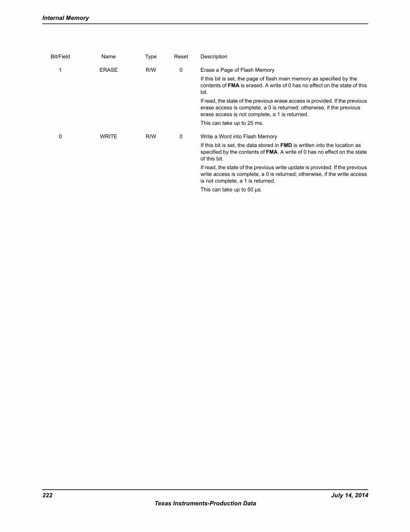
DescriptionResetTypeNameBit/Field
Erase a Page of Flash MemoryIf this bit is set, the page of flash main memory as specified by thecontents of FMA is erased. A write of 0 has no effect on the state of thisbit.If read, the state of the previous erase access is provided. If the previouserase access is complete, a 0 is returned; otherwise, if the previouserase access is not complete, a 1 is returned.This can take up to 25 ms.
0R/WERASE1
Write a Word into Flash MemoryIf this bit is set, the data stored in FMD is written into the location asspecified by the contents of FMA. A write of 0 has no effect on the stateof this bit.If read, the state of the previous write update is provided. If the previouswrite access is complete, a 0 is returned; otherwise, if the write accessis not complete, a 1 is returned.This can take up to 50 µs.
0R/WWRITE0
July 14, 2014222Texas Instruments-Production Data
Internal Memory
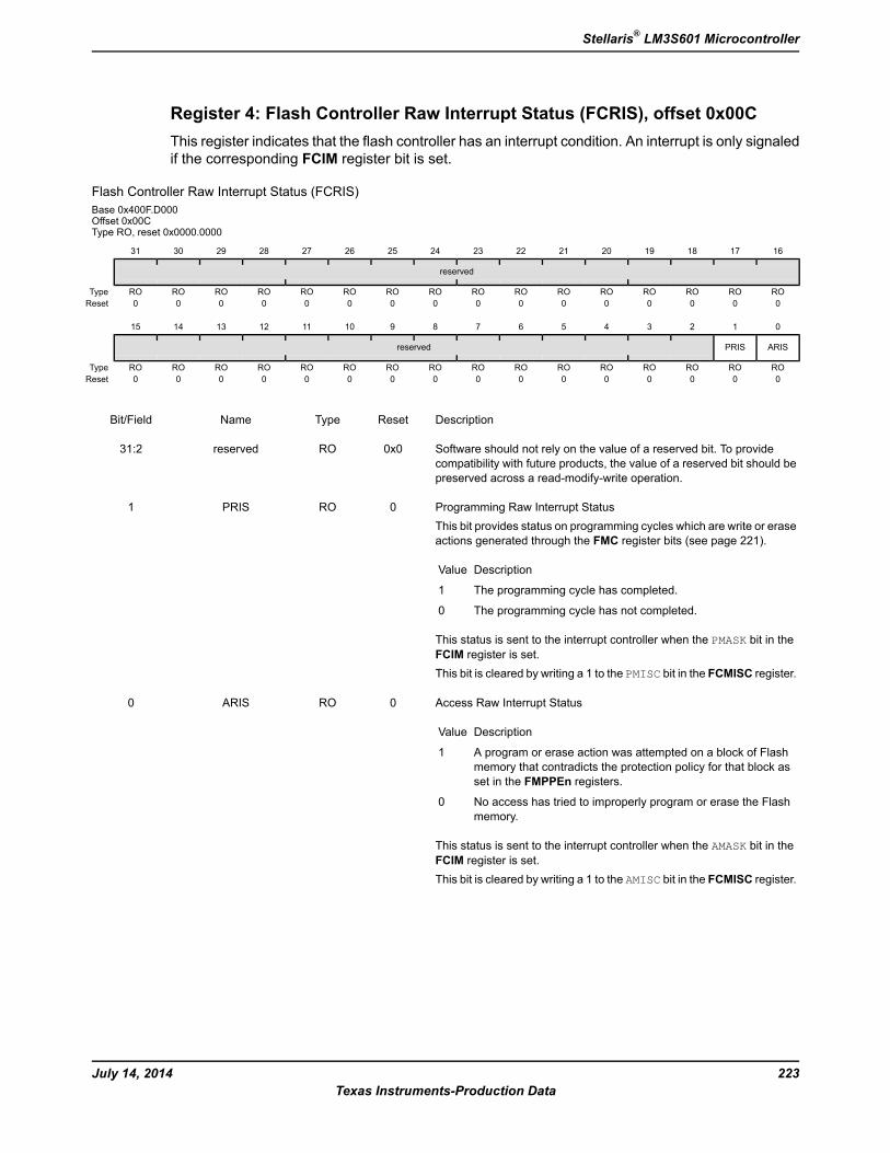
Register 4: Flash Controller Raw Interrupt Status (FCRIS), offset 0x00CThis register indicates that the flash controller has an interrupt condition. An interrupt is only signaledif the corresponding FCIM register bit is set.
Flash Controller Raw Interrupt Status (FCRIS)Base 0x400F.D000Offset 0x00CType RO, reset 0x0000.0000
16171819202122232425262728293031
reserved
ROROROROROROROROROROROROROROROROType0000000000000000Reset
0123456789101112131415
ARISPRISreserved
ROROROROROROROROROROROROROROROROType0000000000000000Reset
DescriptionResetTypeNameBit/Field
Software should not rely on the value of a reserved bit. To providecompatibility with future products, the value of a reserved bit should bepreserved across a read-modify-write operation.
0x0ROreserved31:2
Programming Raw Interrupt StatusThis bit provides status on programming cycles which are write or eraseactions generated through the FMC register bits (see page 221).
DescriptionValue
The programming cycle has completed.1
The programming cycle has not completed.0
This status is sent to the interrupt controller when the PMASK bit in theFCIM register is set.This bit is cleared by writing a 1 to the PMISC bit in the FCMISC register.
0ROPRIS1
Access Raw Interrupt Status
DescriptionValue
A program or erase action was attempted on a block of Flashmemory that contradicts the protection policy for that block asset in the FMPPEn registers.
1
No access has tried to improperly program or erase the Flashmemory.
0
This status is sent to the interrupt controller when the AMASK bit in theFCIM register is set.This bit is cleared by writing a 1 to the AMISC bit in the FCMISC register.
0ROARIS0
223July 14, 2014Texas Instruments-Production Data
Stellaris® LM3S601 Microcontroller
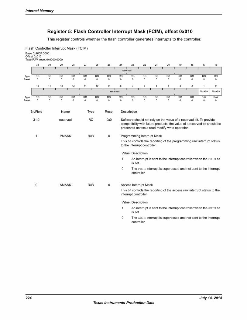
Register 5: Flash Controller Interrupt Mask (FCIM), offset 0x010This register controls whether the flash controller generates interrupts to the controller.
Flash Controller Interrupt Mask (FCIM)Base 0x400F.D000Offset 0x010Type R/W, reset 0x0000.0000
16171819202122232425262728293031
reserved
ROROROROROROROROROROROROROROROROType0000000000000000Reset
0123456789101112131415
AMASKPMASKreserved
R/WR/WROROROROROROROROROROROROROROType0000000000000000Reset
DescriptionResetTypeNameBit/Field
Software should not rely on the value of a reserved bit. To providecompatibility with future products, the value of a reserved bit should bepreserved across a read-modify-write operation.
0x0ROreserved31:2
Programming Interrupt MaskThis bit controls the reporting of the programming raw interrupt statusto the interrupt controller.
DescriptionValue
An interrupt is sent to the interrupt controller when the PRIS bitis set.
1
The PRIS interrupt is suppressed and not sent to the interruptcontroller.
0
0R/WPMASK1
Access Interrupt MaskThis bit controls the reporting of the access raw interrupt status to theinterrupt controller.
DescriptionValue
An interrupt is sent to the interrupt controller when the ARIS bitis set.
1
The ARIS interrupt is suppressed and not sent to the interruptcontroller.
0
0R/WAMASK0
July 14, 2014224Texas Instruments-Production Data
Internal Memory
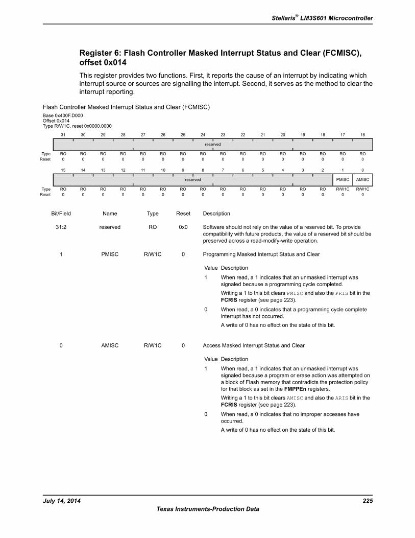
Register 6: Flash Controller Masked Interrupt Status and Clear (FCMISC),offset 0x014This register provides two functions. First, it reports the cause of an interrupt by indicating whichinterrupt source or sources are signalling the interrupt. Second, it serves as the method to clear theinterrupt reporting.
Flash Controller Masked Interrupt Status and Clear (FCMISC)Base 0x400F.D000Offset 0x014Type R/W1C, reset 0x0000.0000
16171819202122232425262728293031
reserved
ROROROROROROROROROROROROROROROROType0000000000000000Reset
0123456789101112131415
AMISCPMISCreserved
R/W1CR/W1CROROROROROROROROROROROROROROType0000000000000000Reset
DescriptionResetTypeNameBit/Field
Software should not rely on the value of a reserved bit. To providecompatibility with future products, the value of a reserved bit should bepreserved across a read-modify-write operation.
0x0ROreserved31:2
Programming Masked Interrupt Status and Clear
DescriptionValue
When read, a 1 indicates that an unmasked interrupt wassignaled because a programming cycle completed.Writing a 1 to this bit clears PMISC and also the PRIS bit in theFCRIS register (see page 223).
1
When read, a 0 indicates that a programming cycle completeinterrupt has not occurred.A write of 0 has no effect on the state of this bit.
0
0R/W1CPMISC1
Access Masked Interrupt Status and Clear
DescriptionValue
When read, a 1 indicates that an unmasked interrupt wassignaled because a program or erase action was attempted ona block of Flash memory that contradicts the protection policyfor that block as set in the FMPPEn registers.Writing a 1 to this bit clears AMISC and also the ARIS bit in theFCRIS register (see page 223).
1
When read, a 0 indicates that no improper accesses haveoccurred.A write of 0 has no effect on the state of this bit.
0
0R/W1CAMISC0
225July 14, 2014Texas Instruments-Production Data
Stellaris® LM3S601 Microcontroller
6.6 Flash Register Descriptions (System Control Offset)The remainder of this section lists and describes the Flash Memory registers, in numerical order byaddress offset. Registers in this section are relative to the System Control base address of0x400F.E000.
July 14, 2014226Texas Instruments-Production Data
Internal Memory
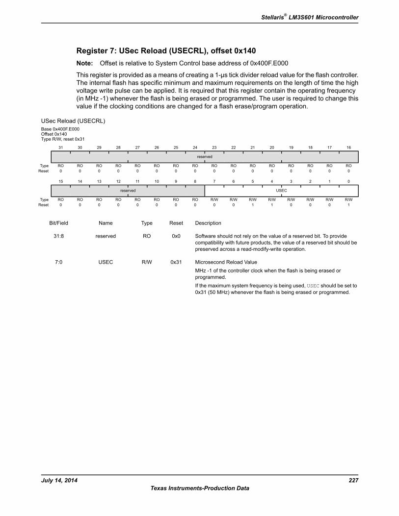
Register 7: USec Reload (USECRL), offset 0x140Note: Offset is relative to System Control base address of 0x400F.E000
This register is provided as a means of creating a 1-μs tick divider reload value for the flash controller.The internal flash has specific minimum and maximum requirements on the length of time the highvoltage write pulse can be applied. It is required that this register contain the operating frequency(in MHz -1) whenever the flash is being erased or programmed. The user is required to change thisvalue if the clocking conditions are changed for a flash erase/program operation.
USec Reload (USECRL)Base 0x400F.E000Offset 0x140Type R/W, reset 0x31
16171819202122232425262728293031
reserved
ROROROROROROROROROROROROROROROROType0000000000000000Reset
0123456789101112131415
USECreserved
R/WR/WR/WR/WR/WR/WR/WR/WROROROROROROROROType1000110000000000Reset
DescriptionResetTypeNameBit/Field
Software should not rely on the value of a reserved bit. To providecompatibility with future products, the value of a reserved bit should bepreserved across a read-modify-write operation.
0x0ROreserved31:8
Microsecond Reload ValueMHz -1 of the controller clock when the flash is being erased orprogrammed.If the maximum system frequency is being used, USEC should be set to0x31 (50 MHz) whenever the flash is being erased or programmed.
0x31R/WUSEC7:0
227July 14, 2014Texas Instruments-Production Data
Stellaris® LM3S601 Microcontroller
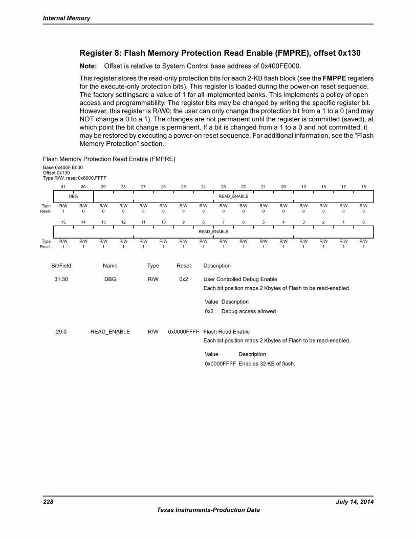
Register 8: Flash Memory Protection Read Enable (FMPRE), offset 0x130Note: Offset is relative to System Control base address of 0x400FE000.
This register stores the read-only protection bits for each 2-KB flash block (see the FMPPE registersfor the execute-only protection bits). This register is loaded during the power-on reset sequence.The factory settingsare a value of 1 for all implemented banks. This implements a policy of openaccess and programmability. The register bits may be changed by writing the specific register bit.However, this register is R/W0; the user can only change the protection bit from a 1 to a 0 (and mayNOT change a 0 to a 1). The changes are not permanent until the register is committed (saved), atwhich point the bit change is permanent. If a bit is changed from a 1 to a 0 and not committed, itmay be restored by executing a power-on reset sequence. For additional information, see the “FlashMemory Protection” section.
Flash Memory Protection Read Enable (FMPRE)Base 0x400F.E000Offset 0x130Type R/W, reset 0x8000.FFFF
16171819202122232425262728293031
READ_ENABLEDBG
R/WR/WR/WR/WR/WR/WR/WR/WR/WR/WR/WR/WR/WR/WR/WR/WType0000000000000001Reset
0123456789101112131415
READ_ENABLE
R/WR/WR/WR/WR/WR/WR/WR/WR/WR/WR/WR/WR/WR/WR/WR/WType1111111111111111Reset
DescriptionResetTypeNameBit/Field
User Controlled Debug EnableEach bit position maps 2 Kbytes of Flash to be read-enabled.
DescriptionValue
Debug access allowed0x2
0x2R/WDBG31:30
Flash Read EnableEach bit position maps 2 Kbytes of Flash to be read-enabled.
DescriptionValue
Enables 32 KB of flash.0x0000FFFF
0x0000FFFFR/WREAD_ENABLE29:0
July 14, 2014228Texas Instruments-Production Data
Internal Memory
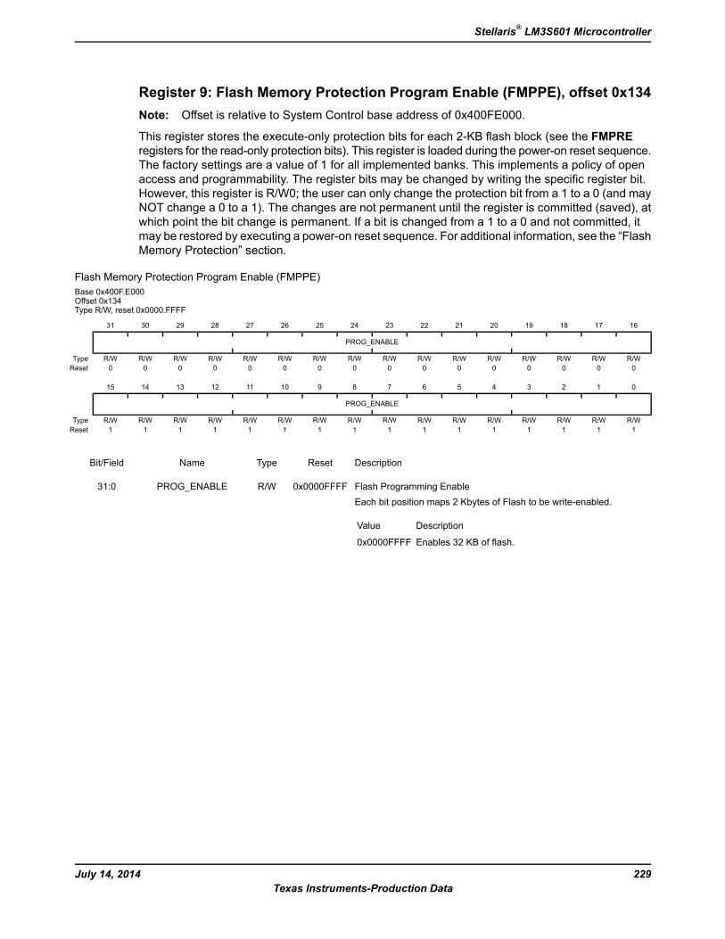
Register 9: Flash Memory Protection Program Enable (FMPPE), offset 0x134Note: Offset is relative to System Control base address of 0x400FE000.
This register stores the execute-only protection bits for each 2-KB flash block (see the FMPREregisters for the read-only protection bits). This register is loaded during the power-on reset sequence.The factory settings are a value of 1 for all implemented banks. This implements a policy of openaccess and programmability. The register bits may be changed by writing the specific register bit.However, this register is R/W0; the user can only change the protection bit from a 1 to a 0 (and mayNOT change a 0 to a 1). The changes are not permanent until the register is committed (saved), atwhich point the bit change is permanent. If a bit is changed from a 1 to a 0 and not committed, itmay be restored by executing a power-on reset sequence. For additional information, see the “FlashMemory Protection” section.
Flash Memory Protection Program Enable (FMPPE)Base 0x400F.E000Offset 0x134Type R/W, reset 0x0000.FFFF
16171819202122232425262728293031
PROG_ENABLE
R/WR/WR/WR/WR/WR/WR/WR/WR/WR/WR/WR/WR/WR/WR/WR/WType0000000000000000Reset
0123456789101112131415
PROG_ENABLE
R/WR/WR/WR/WR/WR/WR/WR/WR/WR/WR/WR/WR/WR/WR/WR/WType1111111111111111Reset
DescriptionResetTypeNameBit/Field
Flash Programming EnableEach bit position maps 2 Kbytes of Flash to be write-enabled.
DescriptionValue
Enables 32 KB of flash.0x0000FFFF
0x0000FFFFR/WPROG_ENABLE31:0
229July 14, 2014Texas Instruments-Production Data
Stellaris® LM3S601 Microcontroller
7 General-Purpose Input/Outputs (GPIOs)The GPIO module is composed of five physical GPIO blocks, each corresponding to an individualGPIO port (Port A, Port B, Port C, Port D, Port E). The GPIO module supports 0-36 programmableinput/output pins, depending on the peripherals being used.
The GPIO module has the following features:
0-36 GPIOs, depending on configuration
5-V-tolerant in input configuration
Fast toggle capable of a change every two clock cycles
Programmable control for GPIO interrupts
– Interrupt generation masking
– Edge-triggered on rising, falling, or both
– Level-sensitive on High or Low values
Bit masking in both read and write operations through address lines
Pins configured as digital inputs are Schmitt-triggered.
Programmable control for GPIO pad configuration
– Weak pull-up or pull-down resistors
– 2-mA, 4-mA, and 8-mA pad drive for digital communication
– Slew rate control for the 8-mA drive
– Open drain enables
– Digital input enables
July 14, 2014230Texas Instruments-Production Data
General-Purpose Input/Outputs (GPIOs)
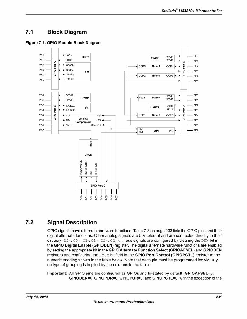
7.1 Block Diagram
Figure 7-1. GPIO Module Block Diagram
GPIOPo
rtD
SSIClk
SSIFss
UART0
SSI
PWM1
I2CSCLI2CSDA
I2C
AnalogComparators
C2-
PWM4PWM5
U1RxU1Tx
PWM0PWM1
PhBPhA
TCK/SWCLK
TMS/SWDIO
TDI
TDO/SWO
TRST
PWM2
JTAG
CCP5 Timer2 CCP4
CCP2 Timer1 CCP3
CCP1 Timer0 CCP0
UART1
Fault PWM0
IDXQEI
PA0
PA1
PA2
PA3
PA4
PA5
PE0
PE1
PE2
PE3
PE4
PE5
PB0
PB1
PB2
PB3
PB4
PB5
PB6
PB7
PD0
PD1
PD2
PD3
PD4
PD5
PD6
PD7
PC0
PC1
PC2
PC3
PC4
PC5
PC6
PC7
GPIOPo
rtE
GPIOPo
rtA
GPIOPo
rtB
GPIO Port C
U0Rx
U0Tx
SSIRx
SSITx
PWM2
PWM3
C0-
C1-
C0+
C2+
C0o/C1+
7.2 Signal DescriptionGPIO signals have alternate hardware functions. Table 7-3 on page 233 lists the GPIO pins and theirdigital alternate functions. Other analog signals are 5-V tolerant and are connected directly to theircircuitry (C0-, C0+, C1-, C1+, C2-, C2+). These signals are configured by clearing the DEN bit intheGPIO Digital Enable (GPIODEN) register. The digital alternate hardware functions are enabledby setting the appropriate bit in theGPIO Alternate Function Select (GPIOAFSEL) andGPIODENregisters and configuring the PMCx bit field in the GPIO Port Control (GPIOPCTL) register to thenumeric enoding shown in the table below. Note that each pin must be programmed individually;no type of grouping is implied by the columns in the table.
Important: All GPIO pins are configured as GPIOs and tri-stated by default (GPIOAFSEL=0,GPIODEN=0,GPIOPDR=0,GPIOPUR=0, andGPIOPCTL=0, with the exception of the
231July 14, 2014Texas Instruments-Production Data
Stellaris® LM3S601 Microcontroller
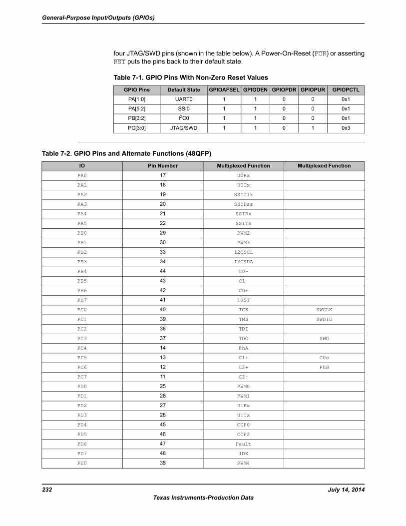
four JTAG/SWD pins (shown in the table below). A Power-On-Reset (POR) or assertingRST puts the pins back to their default state.
Table 7-1. GPIO Pins With Non-Zero Reset Values
GPIOPCTLGPIOPURGPIOPDRGPIODENGPIOAFSELDefault StateGPIO Pins
0x10011UART0PA[1:0]
0x10011SSI0PA[5:2]
0x10011I2C0PB[3:2]
0x31011JTAG/SWDPC[3:0]
Table 7-2. GPIO Pins and Alternate Functions (48QFP)
Multiplexed FunctionMultiplexed FunctionPin NumberIO
U0Rx17PA0
U0Tx18PA1
SSIClk19PA2
SSIFss20PA3
SSIRx21PA4
SSITx22PA5
PWM229PB0
PWM330PB1
I2CSCL33PB2
I2CSDA34PB3
C0-44PB4
C1-43PB5
C0+42PB6
TRST41PB7
SWCLKTCK40PC0
SWDIOTMS39PC1
TDI38PC2
SWOTDO37PC3
PhA14PC4
C0oC1+13PC5
PhBC2+12PC6
C2-11PC7
PWM025PD0
PWM126PD1
U1Rx27PD2
U1Tx28PD3
CCP045PD4
CCP246PD5
Fault47PD6
IDX48PD7
PWM435PE0
July 14, 2014232Texas Instruments-Production Data
General-Purpose Input/Outputs (GPIOs)
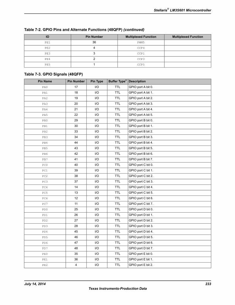
Table 7-2. GPIO Pins and Alternate Functions (48QFP) (continued)
Multiplexed FunctionMultiplexed FunctionPin NumberIO
PWM536PE1
CCP44PE2
CCP13PE3
CCP32PE4
CCP51PE5
Table 7-3. GPIO Signals (48QFP)
DescriptionBuffer TypeaPin TypePin NumberPin Name
GPIO port A bit 0.TTLI/O17PA0
GPIO port A bit 1.TTLI/O18PA1
GPIO port A bit 2.TTLI/O19PA2
GPIO port A bit 3.TTLI/O20PA3
GPIO port A bit 4.TTLI/O21PA4
GPIO port A bit 5.TTLI/O22PA5
GPIO port B bit 0.TTLI/O29PB0
GPIO port B bit 1.TTLI/O30PB1
GPIO port B bit 2.TTLI/O33PB2
GPIO port B bit 3.TTLI/O34PB3
GPIO port B bit 4.TTLI/O44PB4
GPIO port B bit 5.TTLI/O43PB5
GPIO port B bit 6.TTLI/O42PB6
GPIO port B bit 7.TTLI/O41PB7
GPIO port C bit 0.TTLI/O40PC0
GPIO port C bit 1.TTLI/O39PC1
GPIO port C bit 2.TTLI/O38PC2
GPIO port C bit 3.TTLI/O37PC3
GPIO port C bit 4.TTLI/O14PC4
GPIO port C bit 5.TTLI/O13PC5
GPIO port C bit 6.TTLI/O12PC6
GPIO port C bit 7.TTLI/O11PC7
GPIO port D bit 0.TTLI/O25PD0
GPIO port D bit 1.TTLI/O26PD1
GPIO port D bit 2.TTLI/O27PD2
GPIO port D bit 3.TTLI/O28PD3
GPIO port D bit 4.TTLI/O45PD4
GPIO port D bit 5.TTLI/O46PD5
GPIO port D bit 6.TTLI/O47PD6
GPIO port D bit 7.TTLI/O48PD7
GPIO port E bit 0.TTLI/O35PE0
GPIO port E bit 1.TTLI/O36PE1
GPIO port E bit 2.TTLI/O4PE2
233July 14, 2014Texas Instruments-Production Data
Stellaris® LM3S601 Microcontroller
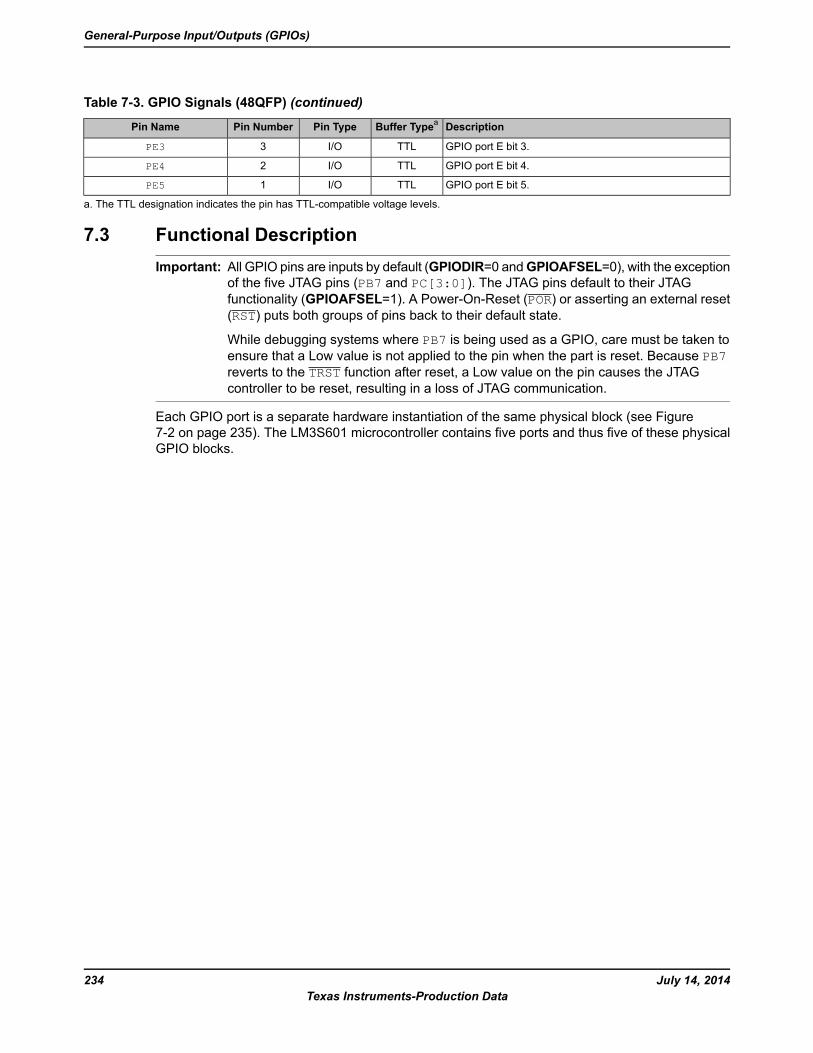
Table 7-3. GPIO Signals (48QFP) (continued)
DescriptionBuffer TypeaPin TypePin NumberPin Name
GPIO port E bit 3.TTLI/O3PE3
GPIO port E bit 4.TTLI/O2PE4
GPIO port E bit 5.TTLI/O1PE5
a. The TTL designation indicates the pin has TTL-compatible voltage levels.
7.3 Functional DescriptionImportant: All GPIO pins are inputs by default (GPIODIR=0 andGPIOAFSEL=0), with the exception
of the five JTAG pins (PB7 and PC[3:0]). The JTAG pins default to their JTAGfunctionality (GPIOAFSEL=1). A Power-On-Reset (POR) or asserting an external reset(RST) puts both groups of pins back to their default state.
While debugging systems where PB7 is being used as a GPIO, care must be taken toensure that a Low value is not applied to the pin when the part is reset. Because PB7reverts to the TRST function after reset, a Low value on the pin causes the JTAGcontroller to be reset, resulting in a loss of JTAG communication.
Each GPIO port is a separate hardware instantiation of the same physical block (see Figure7-2 on page 235). The LM3S601 microcontroller contains five ports and thus five of these physicalGPIO blocks.
July 14, 2014234Texas Instruments-Production Data
General-Purpose Input/Outputs (GPIOs)
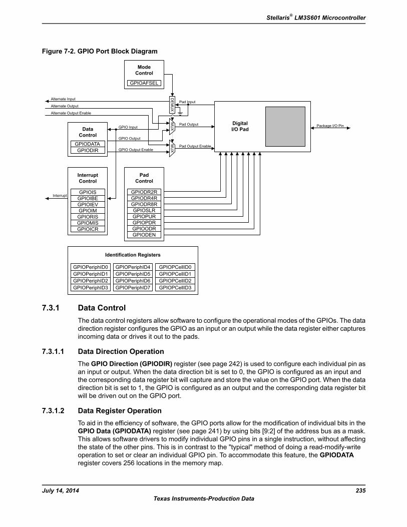
Figure 7-2. GPIO Port Block Diagram
Alternate Input
Alternate Output
Alternate Output Enable
Interrupt
GPIO Input
GPIO Output
GPIO Output Enable
Pad Output
Pad Output Enable
Package I/O PinData
Control
GPIOISGPIOIBEGPIOIEVGPIOIMGPIORISGPIOMISGPIOICR
InterruptControl
GPIODR2RGPIODR4RGPIODR8RGPIOSLRGPIOPURGPIOPDRGPIOODRGPIODEN
PadControl
GPIOPeriphID0GPIOPeriphID1GPIOPeriphID2GPIOPeriphID3
GPIOPeriphID4GPIOPeriphID5GPIOPeriphID6GPIOPeriphID7
GPIOPCellID0GPIOPCellID1GPIOPCellID2GPIOPCellID3
Identification Registers
GPIOAFSEL
ModeControl
MUX
MUX
DEMUX
DigitalI/O Pad
Pad Input
GPIODATAGPIODIR
7.3.1 Data ControlThe data control registers allow software to configure the operational modes of the GPIOs. The datadirection register configures the GPIO as an input or an output while the data register either capturesincoming data or drives it out to the pads.
7.3.1.1 Data Direction OperationThe GPIO Direction (GPIODIR) register (see page 242) is used to configure each individual pin asan input or output. When the data direction bit is set to 0, the GPIO is configured as an input andthe corresponding data register bit will capture and store the value on the GPIO port. When the datadirection bit is set to 1, the GPIO is configured as an output and the corresponding data register bitwill be driven out on the GPIO port.
7.3.1.2 Data Register OperationTo aid in the efficiency of software, the GPIO ports allow for the modification of individual bits in theGPIO Data (GPIODATA) register (see page 241) by using bits [9:2] of the address bus as a mask.This allows software drivers to modify individual GPIO pins in a single instruction, without affectingthe state of the other pins. This is in contrast to the "typical" method of doing a read-modify-writeoperation to set or clear an individual GPIO pin. To accommodate this feature, the GPIODATAregister covers 256 locations in the memory map.
235July 14, 2014Texas Instruments-Production Data
Stellaris® LM3S601 Microcontroller
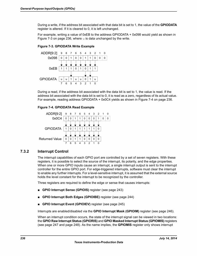
During a write, if the address bit associated with that data bit is set to 1, the value of the GPIODATAregister is altered. If it is cleared to 0, it is left unchanged.
For example, writing a value of 0xEB to the address GPIODATA + 0x098 would yield as shown inFigure 7-3 on page 236, where u is data unchanged by the write.
Figure 7-3. GPIODATA Write Example
0 10 0 1 10 0 0
u 1u u 0 1u u
9 8 7 6 5 4 3 2 1 0
1 11 0 0 11 1
7 6 5 4 3 2 1 0GPIODATA
0xEB
0x098ADDR[9:2]
0
During a read, if the address bit associated with the data bit is set to 1, the value is read. If theaddress bit associated with the data bit is set to 0, it is read as a zero, regardless of its actual value.For example, reading address GPIODATA + 0x0C4 yields as shown in Figure 7-4 on page 236.
Figure 7-4. GPIODATA Read Example
0 10 1 0 00 1 0 0
0 10 1 0 00 0
9 8 7 6 5 4 3 2 1 0
0 11 1 1 11 0
7 6 5 4 3 2 1 0Returned Value
GPIODATA
0x0C4ADDR[9:2]
7.3.2 Interrupt ControlThe interrupt capabilities of each GPIO port are controlled by a set of seven registers. With theseregisters, it is possible to select the source of the interrupt, its polarity, and the edge properties.When one or more GPIO inputs cause an interrupt, a single interrupt output is sent to the interruptcontroller for the entire GPIO port. For edge-triggered interrupts, software must clear the interruptto enable any further interrupts. For a level-sensitive interrupt, it is assumed that the external sourceholds the level constant for the interrupt to be recognized by the controller.
Three registers are required to define the edge or sense that causes interrupts:
GPIO Interrupt Sense (GPIOIS) register (see page 243)
GPIO Interrupt Both Edges (GPIOIBE) register (see page 244)
GPIO Interrupt Event (GPIOIEV) register (see page 245)
Interrupts are enabled/disabled via the GPIO Interrupt Mask (GPIOIM) register (see page 246).
When an interrupt condition occurs, the state of the interrupt signal can be viewed in two locations:theGPIORaw Interrupt Status (GPIORIS) andGPIOMasked Interrupt Status (GPIOMIS) registers(see page 247 and page 248). As the name implies, the GPIOMIS register only shows interrupt
July 14, 2014236Texas Instruments-Production Data
General-Purpose Input/Outputs (GPIOs)
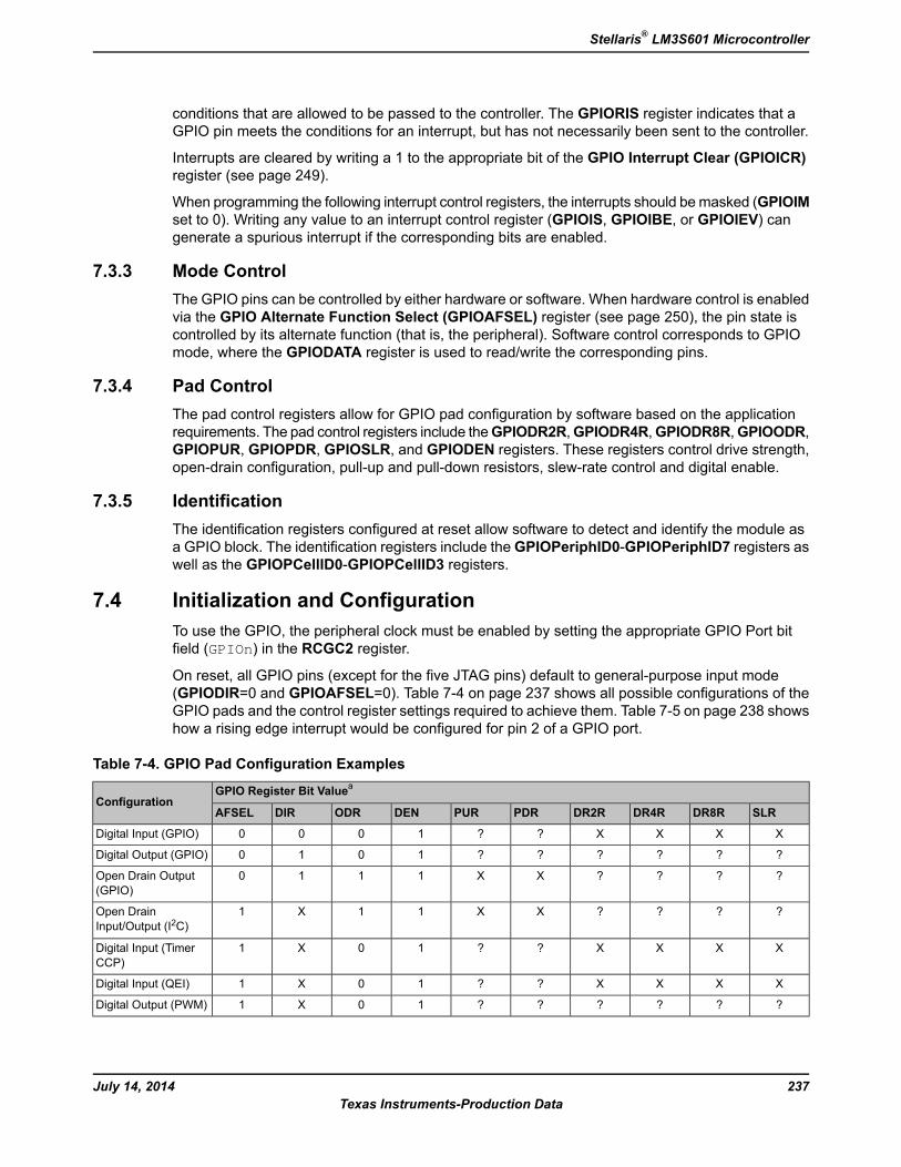
conditions that are allowed to be passed to the controller. The GPIORIS register indicates that aGPIO pin meets the conditions for an interrupt, but has not necessarily been sent to the controller.
Interrupts are cleared by writing a 1 to the appropriate bit of the GPIO Interrupt Clear (GPIOICR)register (see page 249).
When programming the following interrupt control registers, the interrupts should bemasked (GPIOIMset to 0). Writing any value to an interrupt control register (GPIOIS, GPIOIBE, or GPIOIEV) cangenerate a spurious interrupt if the corresponding bits are enabled.
7.3.3 Mode ControlThe GPIO pins can be controlled by either hardware or software. When hardware control is enabledvia the GPIO Alternate Function Select (GPIOAFSEL) register (see page 250), the pin state iscontrolled by its alternate function (that is, the peripheral). Software control corresponds to GPIOmode, where the GPIODATA register is used to read/write the corresponding pins.
7.3.4 Pad ControlThe pad control registers allow for GPIO pad configuration by software based on the applicationrequirements. The pad control registers include theGPIODR2R,GPIODR4R,GPIODR8R,GPIOODR,GPIOPUR, GPIOPDR, GPIOSLR, and GPIODEN registers. These registers control drive strength,open-drain configuration, pull-up and pull-down resistors, slew-rate control and digital enable.
7.3.5 IdentificationThe identification registers configured at reset allow software to detect and identify the module asa GPIO block. The identification registers include theGPIOPeriphID0-GPIOPeriphID7 registers aswell as the GPIOPCellID0-GPIOPCellID3 registers.
7.4 Initialization and ConfigurationTo use the GPIO, the peripheral clock must be enabled by setting the appropriate GPIO Port bitfield (GPIOn) in the RCGC2 register.
On reset, all GPIO pins (except for the five JTAG pins) default to general-purpose input mode(GPIODIR=0 and GPIOAFSEL=0). Table 7-4 on page 237 shows all possible configurations of theGPIO pads and the control register settings required to achieve them. Table 7-5 on page 238 showshow a rising edge interrupt would be configured for pin 2 of a GPIO port.
Table 7-4. GPIO Pad Configuration Examples
GPIO Register Bit ValueaConfiguration
SLRDR8RDR4RDR2RPDRPURDENODRDIRAFSEL
XXXX??1000Digital Input (GPIO)
??????1010Digital Output (GPIO)
????XX1110Open Drain Output(GPIO)
????XX11X1Open DrainInput/Output (I2C)
XXXX??10X1Digital Input (TimerCCP)
XXXX??10X1Digital Input (QEI)
??????10X1Digital Output (PWM)
237July 14, 2014Texas Instruments-Production Data
Stellaris® LM3S601 Microcontroller
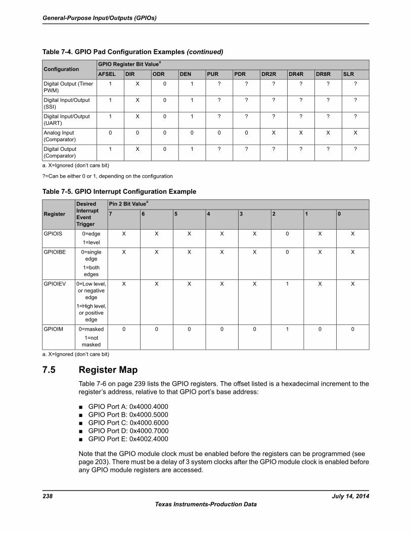
Table 7-4. GPIO Pad Configuration Examples (continued)
GPIO Register Bit ValueaConfiguration
SLRDR8RDR4RDR2RPDRPURDENODRDIRAFSEL
??????10X1Digital Output (TimerPWM)
??????10X1Digital Input/Output(SSI)
??????10X1Digital Input/Output(UART)
XXXX000000Analog Input(Comparator)
??????10X1Digital Output(Comparator)
a. X=Ignored (don’t care bit)
?=Can be either 0 or 1, depending on the configuration
Table 7-5. GPIO Interrupt Configuration Example
Pin 2 Bit ValueaDesiredInterruptEventTrigger
Register 01234567
XX0XXXXX0=edge1=level
GPIOIS
XX0XXXXX0=singleedge1=bothedges
GPIOIBE
XX1XXXXX0=Low level,or negative
edge1=High level,or positiveedge
GPIOIEV
001000000=masked1=notmasked
GPIOIM
a. X=Ignored (don’t care bit)
7.5 Register MapTable 7-6 on page 239 lists the GPIO registers. The offset listed is a hexadecimal increment to theregister’s address, relative to that GPIO port’s base address:
GPIO Port A: 0x4000.4000 GPIO Port B: 0x4000.5000 GPIO Port C: 0x4000.6000 GPIO Port D: 0x4000.7000 GPIO Port E: 0x4002.4000
Note that the GPIO module clock must be enabled before the registers can be programmed (seepage 203). There must be a delay of 3 system clocks after the GPIOmodule clock is enabled beforeany GPIO module registers are accessed.
July 14, 2014238Texas Instruments-Production Data
General-Purpose Input/Outputs (GPIOs)
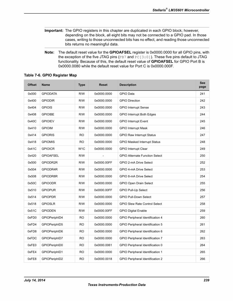
Important: The GPIO registers in this chapter are duplicated in each GPIO block; however,depending on the block, all eight bits may not be connected to a GPIO pad. In thosecases, writing to those unconnected bits has no effect, and reading those unconnectedbits returns no meaningful data.
Note: The default reset value for the GPIOAFSEL register is 0x0000.0000 for all GPIO pins, withthe exception of the five JTAG pins (PB7 and PC[3:0]). These five pins default to JTAGfunctionality. Because of this, the default reset value of GPIOAFSEL for GPIO Port B is0x0000.0080 while the default reset value for Port C is 0x0000.000F.
Table 7-6. GPIO Register Map
SeepageDescriptionResetTypeNameOffset
241GPIO Data0x0000.0000R/WGPIODATA0x000
242GPIO Direction0x0000.0000R/WGPIODIR0x400
243GPIO Interrupt Sense0x0000.0000R/WGPIOIS0x404
244GPIO Interrupt Both Edges0x0000.0000R/WGPIOIBE0x408
245GPIO Interrupt Event0x0000.0000R/WGPIOIEV0x40C
246GPIO Interrupt Mask0x0000.0000R/WGPIOIM0x410
247GPIO Raw Interrupt Status0x0000.0000ROGPIORIS0x414
248GPIO Masked Interrupt Status0x0000.0000ROGPIOMIS0x418
249GPIO Interrupt Clear0x0000.0000W1CGPIOICR0x41C
250GPIO Alternate Function Select-R/WGPIOAFSEL0x420
252GPIO 2-mA Drive Select0x0000.00FFR/WGPIODR2R0x500
253GPIO 4-mA Drive Select0x0000.0000R/WGPIODR4R0x504
254GPIO 8-mA Drive Select0x0000.0000R/WGPIODR8R0x508
255GPIO Open Drain Select0x0000.0000R/WGPIOODR0x50C
256GPIO Pull-Up Select0x0000.00FFR/WGPIOPUR0x510
257GPIO Pull-Down Select0x0000.0000R/WGPIOPDR0x514
258GPIO Slew Rate Control Select0x0000.0000R/WGPIOSLR0x518
259GPIO Digital Enable0x0000.00FFR/WGPIODEN0x51C
260GPIO Peripheral Identification 40x0000.0000ROGPIOPeriphID40xFD0
261GPIO Peripheral Identification 50x0000.0000ROGPIOPeriphID50xFD4
262GPIO Peripheral Identification 60x0000.0000ROGPIOPeriphID60xFD8
263GPIO Peripheral Identification 70x0000.0000ROGPIOPeriphID70xFDC
264GPIO Peripheral Identification 00x0000.0061ROGPIOPeriphID00xFE0
265GPIO Peripheral Identification 10x0000.0000ROGPIOPeriphID10xFE4
266GPIO Peripheral Identification 20x0000.0018ROGPIOPeriphID20xFE8
239July 14, 2014Texas Instruments-Production Data
Stellaris® LM3S601 Microcontroller
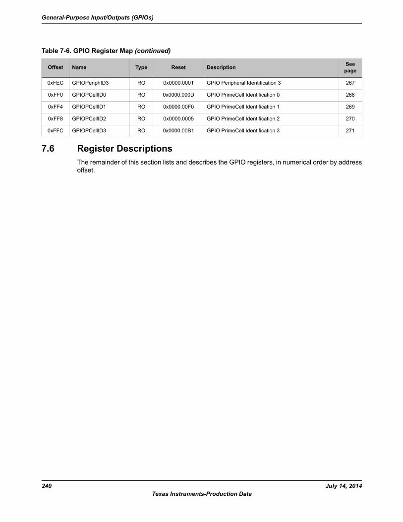
Table 7-6. GPIO Register Map (continued)
SeepageDescriptionResetTypeNameOffset
267GPIO Peripheral Identification 30x0000.0001ROGPIOPeriphID30xFEC
268GPIO PrimeCell Identification 00x0000.000DROGPIOPCellID00xFF0
269GPIO PrimeCell Identification 10x0000.00F0ROGPIOPCellID10xFF4
270GPIO PrimeCell Identification 20x0000.0005ROGPIOPCellID20xFF8
271GPIO PrimeCell Identification 30x0000.00B1ROGPIOPCellID30xFFC
7.6 Register DescriptionsThe remainder of this section lists and describes the GPIO registers, in numerical order by addressoffset.
July 14, 2014240Texas Instruments-Production Data
General-Purpose Input/Outputs (GPIOs)
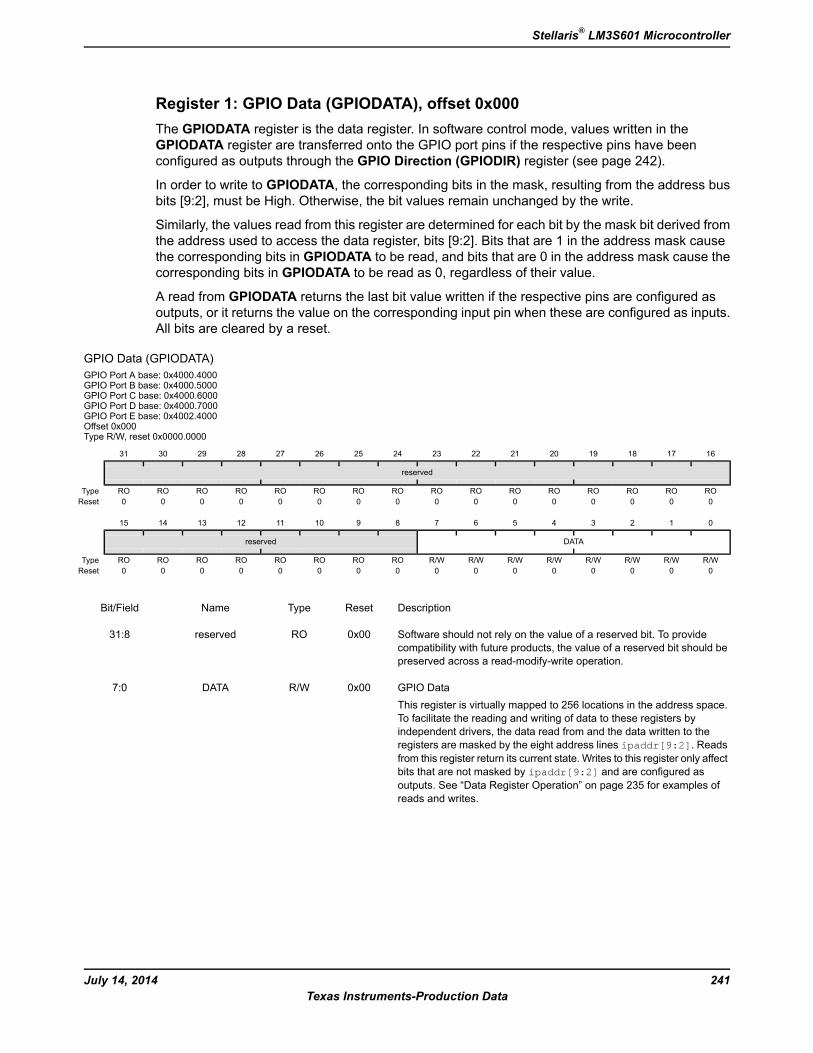
Register 1: GPIO Data (GPIODATA), offset 0x000The GPIODATA register is the data register. In software control mode, values written in theGPIODATA register are transferred onto the GPIO port pins if the respective pins have beenconfigured as outputs through the GPIO Direction (GPIODIR) register (see page 242).
In order to write to GPIODATA, the corresponding bits in the mask, resulting from the address busbits [9:2], must be High. Otherwise, the bit values remain unchanged by the write.
Similarly, the values read from this register are determined for each bit by the mask bit derived fromthe address used to access the data register, bits [9:2]. Bits that are 1 in the address mask causethe corresponding bits in GPIODATA to be read, and bits that are 0 in the address mask cause thecorresponding bits in GPIODATA to be read as 0, regardless of their value.
A read from GPIODATA returns the last bit value written if the respective pins are configured asoutputs, or it returns the value on the corresponding input pin when these are configured as inputs.All bits are cleared by a reset.
GPIO Data (GPIODATA)GPIO Port A base: 0x4000.4000GPIO Port B base: 0x4000.5000GPIO Port C base: 0x4000.6000GPIO Port D base: 0x4000.7000GPIO Port E base: 0x4002.4000Offset 0x000Type R/W, reset 0x0000.0000
16171819202122232425262728293031
reserved
ROROROROROROROROROROROROROROROROType0000000000000000Reset
0123456789101112131415
DATAreserved
R/WR/WR/WR/WR/WR/WR/WR/WROROROROROROROROType0000000000000000Reset
DescriptionResetTypeNameBit/Field
Software should not rely on the value of a reserved bit. To providecompatibility with future products, the value of a reserved bit should bepreserved across a read-modify-write operation.
0x00ROreserved31:8
GPIO DataThis register is virtually mapped to 256 locations in the address space.To facilitate the reading and writing of data to these registers byindependent drivers, the data read from and the data written to theregisters are masked by the eight address lines ipaddr[9:2]. Readsfrom this register return its current state. Writes to this register only affectbits that are not masked by ipaddr[9:2] and are configured asoutputs. See “Data Register Operation” on page 235 for examples ofreads and writes.
0x00R/WDATA7:0
241July 14, 2014Texas Instruments-Production Data
Stellaris® LM3S601 Microcontroller
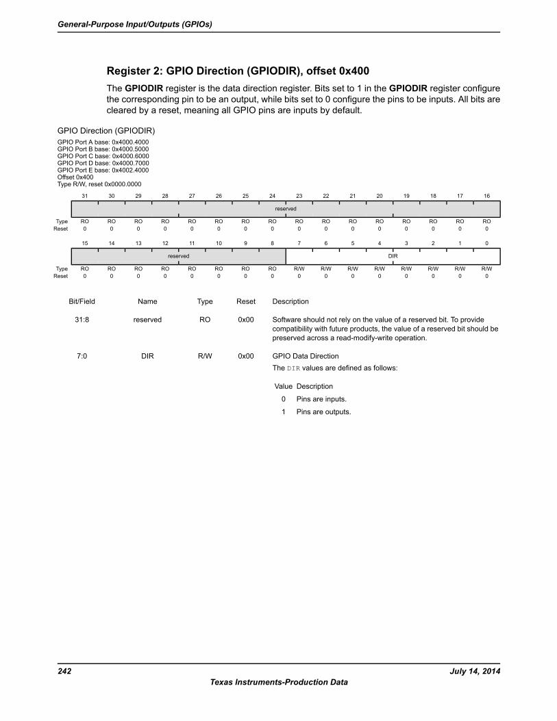
Register 2: GPIO Direction (GPIODIR), offset 0x400The GPIODIR register is the data direction register. Bits set to 1 in the GPIODIR register configurethe corresponding pin to be an output, while bits set to 0 configure the pins to be inputs. All bits arecleared by a reset, meaning all GPIO pins are inputs by default.
GPIO Direction (GPIODIR)GPIO Port A base: 0x4000.4000GPIO Port B base: 0x4000.5000GPIO Port C base: 0x4000.6000GPIO Port D base: 0x4000.7000GPIO Port E base: 0x4002.4000Offset 0x400Type R/W, reset 0x0000.0000
16171819202122232425262728293031
reserved
ROROROROROROROROROROROROROROROROType0000000000000000Reset
0123456789101112131415
DIRreserved
R/WR/WR/WR/WR/WR/WR/WR/WROROROROROROROROType0000000000000000Reset
DescriptionResetTypeNameBit/Field
Software should not rely on the value of a reserved bit. To providecompatibility with future products, the value of a reserved bit should bepreserved across a read-modify-write operation.
0x00ROreserved31:8
GPIO Data DirectionThe DIR values are defined as follows:
DescriptionValue
Pins are inputs.0
Pins are outputs.1
0x00R/WDIR7:0
July 14, 2014242Texas Instruments-Production Data
General-Purpose Input/Outputs (GPIOs)
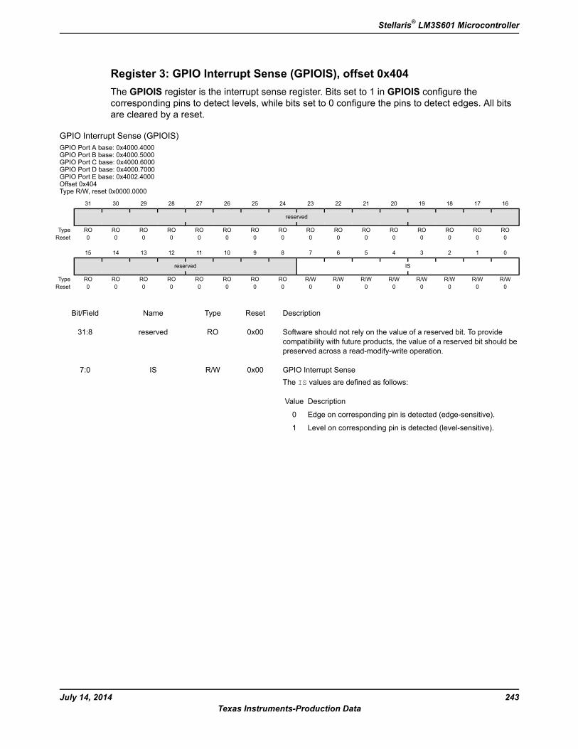
Register 3: GPIO Interrupt Sense (GPIOIS), offset 0x404The GPIOIS register is the interrupt sense register. Bits set to 1 in GPIOIS configure thecorresponding pins to detect levels, while bits set to 0 configure the pins to detect edges. All bitsare cleared by a reset.
GPIO Interrupt Sense (GPIOIS)GPIO Port A base: 0x4000.4000GPIO Port B base: 0x4000.5000GPIO Port C base: 0x4000.6000GPIO Port D base: 0x4000.7000GPIO Port E base: 0x4002.4000Offset 0x404Type R/W, reset 0x0000.0000
16171819202122232425262728293031
reserved
ROROROROROROROROROROROROROROROROType0000000000000000Reset
0123456789101112131415
ISreserved
R/WR/WR/WR/WR/WR/WR/WR/WROROROROROROROROType0000000000000000Reset
DescriptionResetTypeNameBit/Field
Software should not rely on the value of a reserved bit. To providecompatibility with future products, the value of a reserved bit should bepreserved across a read-modify-write operation.
0x00ROreserved31:8
GPIO Interrupt SenseThe IS values are defined as follows:
DescriptionValue
Edge on corresponding pin is detected (edge-sensitive).0
Level on corresponding pin is detected (level-sensitive).1
0x00R/WIS7:0
243July 14, 2014Texas Instruments-Production Data
Stellaris® LM3S601 Microcontroller
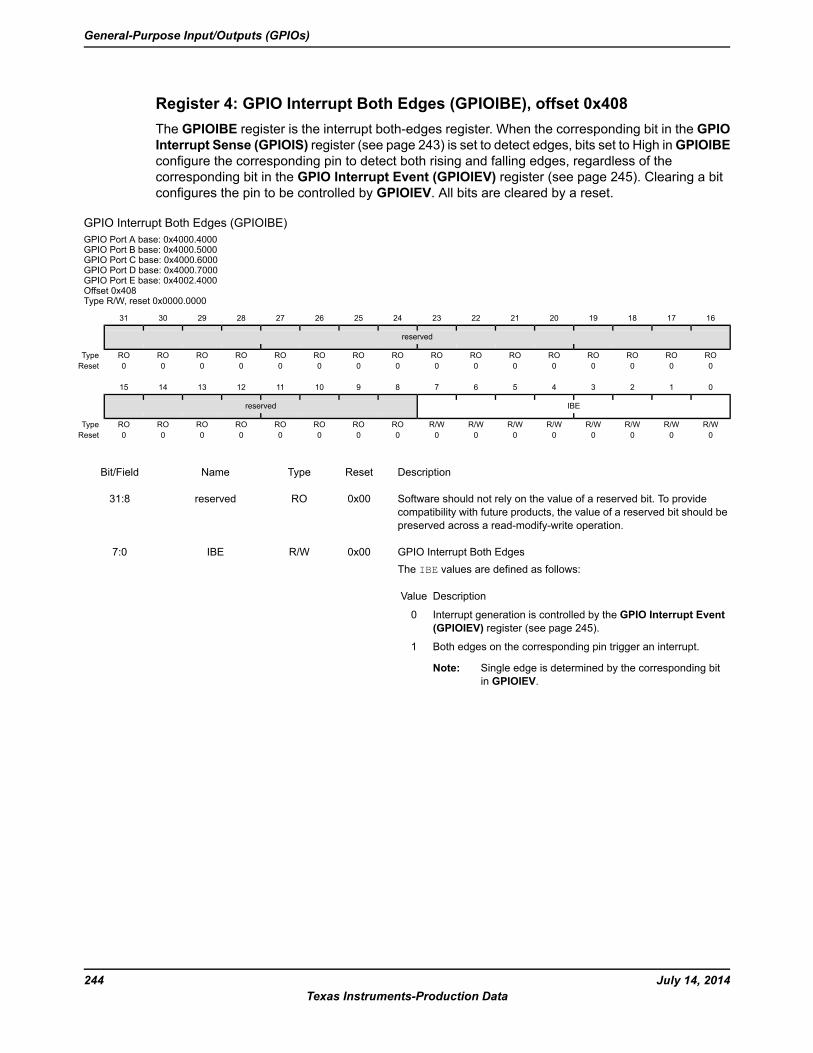
Register 4: GPIO Interrupt Both Edges (GPIOIBE), offset 0x408The GPIOIBE register is the interrupt both-edges register. When the corresponding bit in the GPIOInterrupt Sense (GPIOIS) register (see page 243) is set to detect edges, bits set to High inGPIOIBEconfigure the corresponding pin to detect both rising and falling edges, regardless of thecorresponding bit in the GPIO Interrupt Event (GPIOIEV) register (see page 245). Clearing a bitconfigures the pin to be controlled by GPIOIEV. All bits are cleared by a reset.
GPIO Interrupt Both Edges (GPIOIBE)GPIO Port A base: 0x4000.4000GPIO Port B base: 0x4000.5000GPIO Port C base: 0x4000.6000GPIO Port D base: 0x4000.7000GPIO Port E base: 0x4002.4000Offset 0x408Type R/W, reset 0x0000.0000
16171819202122232425262728293031
reserved
ROROROROROROROROROROROROROROROROType0000000000000000Reset
0123456789101112131415
IBEreserved
R/WR/WR/WR/WR/WR/WR/WR/WROROROROROROROROType0000000000000000Reset
DescriptionResetTypeNameBit/Field
Software should not rely on the value of a reserved bit. To providecompatibility with future products, the value of a reserved bit should bepreserved across a read-modify-write operation.
0x00ROreserved31:8
GPIO Interrupt Both EdgesThe IBE values are defined as follows:
DescriptionValue
Interrupt generation is controlled by the GPIO Interrupt Event(GPIOIEV) register (see page 245).
0
Both edges on the corresponding pin trigger an interrupt.1
Note: Single edge is determined by the corresponding bitin GPIOIEV.
0x00R/WIBE7:0
July 14, 2014244Texas Instruments-Production Data
General-Purpose Input/Outputs (GPIOs)

Register 5: GPIO Interrupt Event (GPIOIEV), offset 0x40CThe GPIOIEV register is the interrupt event register. Bits set to High in GPIOIEV configure thecorresponding pin to detect rising edges or high levels, depending on the corresponding bit valuein the GPIO Interrupt Sense (GPIOIS) register (see page 243). Clearing a bit configures the pin todetect falling edges or low levels, depending on the corresponding bit value in GPIOIS. All bits arecleared by a reset.
GPIO Interrupt Event (GPIOIEV)GPIO Port A base: 0x4000.4000GPIO Port B base: 0x4000.5000GPIO Port C base: 0x4000.6000GPIO Port D base: 0x4000.7000GPIO Port E base: 0x4002.4000Offset 0x40CType R/W, reset 0x0000.0000
16171819202122232425262728293031
reserved
ROROROROROROROROROROROROROROROROType0000000000000000Reset
0123456789101112131415
IEVreserved
R/WR/WR/WR/WR/WR/WR/WR/WROROROROROROROROType0000000000000000Reset
DescriptionResetTypeNameBit/Field
Software should not rely on the value of a reserved bit. To providecompatibility with future products, the value of a reserved bit should bepreserved across a read-modify-write operation.
0x00ROreserved31:8
GPIO Interrupt EventThe IEV values are defined as follows:
DescriptionValue
Falling edge or Low levels on corresponding pins triggerinterrupts.
0
Rising edge or High levels on corresponding pins triggerinterrupts.
1
0x00R/WIEV7:0
245July 14, 2014Texas Instruments-Production Data
Stellaris® LM3S601 Microcontroller
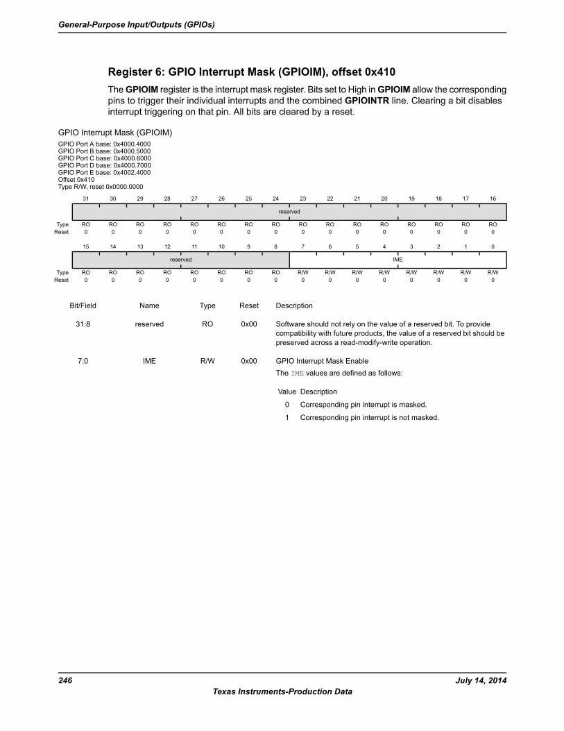
Register 6: GPIO Interrupt Mask (GPIOIM), offset 0x410TheGPIOIM register is the interrupt mask register. Bits set to High inGPIOIM allow the correspondingpins to trigger their individual interrupts and the combined GPIOINTR line. Clearing a bit disablesinterrupt triggering on that pin. All bits are cleared by a reset.
GPIO Interrupt Mask (GPIOIM)GPIO Port A base: 0x4000.4000GPIO Port B base: 0x4000.5000GPIO Port C base: 0x4000.6000GPIO Port D base: 0x4000.7000GPIO Port E base: 0x4002.4000Offset 0x410Type R/W, reset 0x0000.0000
16171819202122232425262728293031
reserved
ROROROROROROROROROROROROROROROROType0000000000000000Reset
0123456789101112131415
IMEreserved
R/WR/WR/WR/WR/WR/WR/WR/WROROROROROROROROType0000000000000000Reset
DescriptionResetTypeNameBit/Field
Software should not rely on the value of a reserved bit. To providecompatibility with future products, the value of a reserved bit should bepreserved across a read-modify-write operation.
0x00ROreserved31:8
GPIO Interrupt Mask EnableThe IME values are defined as follows:
DescriptionValue
Corresponding pin interrupt is masked.0
Corresponding pin interrupt is not masked.1
0x00R/WIME7:0
July 14, 2014246Texas Instruments-Production Data
General-Purpose Input/Outputs (GPIOs)
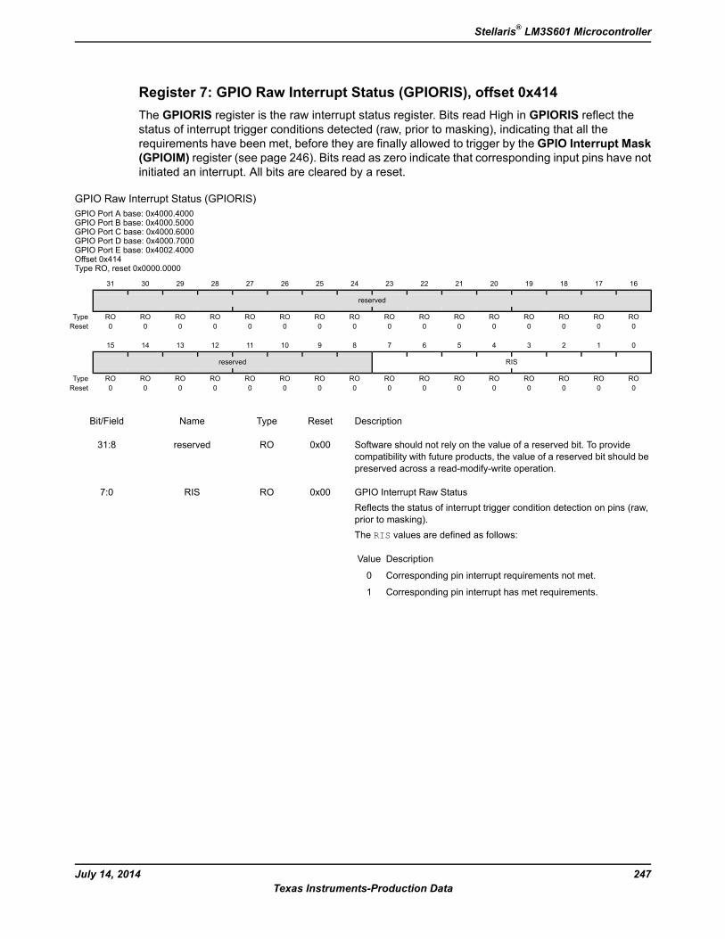
Register 7: GPIO Raw Interrupt Status (GPIORIS), offset 0x414The GPIORIS register is the raw interrupt status register. Bits read High in GPIORIS reflect thestatus of interrupt trigger conditions detected (raw, prior to masking), indicating that all therequirements have been met, before they are finally allowed to trigger by the GPIO Interrupt Mask(GPIOIM) register (see page 246). Bits read as zero indicate that corresponding input pins have notinitiated an interrupt. All bits are cleared by a reset.
GPIO Raw Interrupt Status (GPIORIS)GPIO Port A base: 0x4000.4000GPIO Port B base: 0x4000.5000GPIO Port C base: 0x4000.6000GPIO Port D base: 0x4000.7000GPIO Port E base: 0x4002.4000Offset 0x414Type RO, reset 0x0000.0000
16171819202122232425262728293031
reserved
ROROROROROROROROROROROROROROROROType0000000000000000Reset
0123456789101112131415
RISreserved
ROROROROROROROROROROROROROROROROType0000000000000000Reset
DescriptionResetTypeNameBit/Field
Software should not rely on the value of a reserved bit. To providecompatibility with future products, the value of a reserved bit should bepreserved across a read-modify-write operation.
0x00ROreserved31:8
GPIO Interrupt Raw StatusReflects the status of interrupt trigger condition detection on pins (raw,prior to masking).The RIS values are defined as follows:
DescriptionValue
Corresponding pin interrupt requirements not met.0
Corresponding pin interrupt has met requirements.1
0x00RORIS7:0
247July 14, 2014Texas Instruments-Production Data
Stellaris® LM3S601 Microcontroller
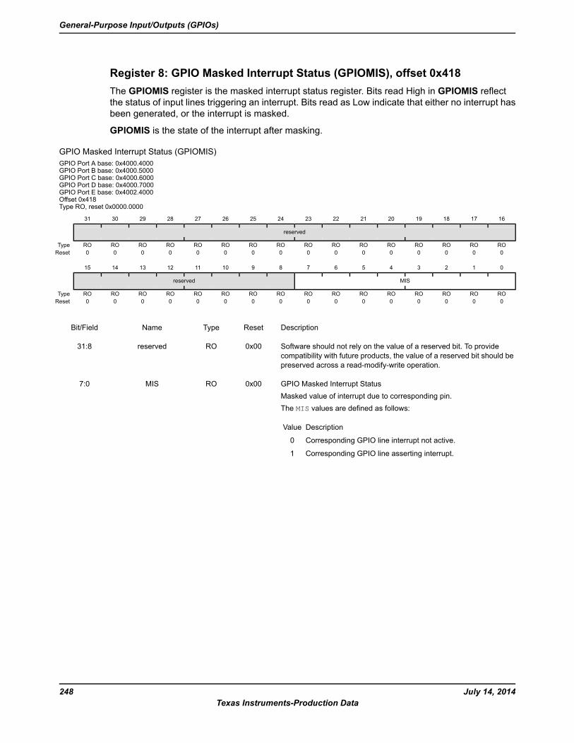
Register 8: GPIO Masked Interrupt Status (GPIOMIS), offset 0x418The GPIOMIS register is the masked interrupt status register. Bits read High in GPIOMIS reflectthe status of input lines triggering an interrupt. Bits read as Low indicate that either no interrupt hasbeen generated, or the interrupt is masked.
GPIOMIS is the state of the interrupt after masking.
GPIO Masked Interrupt Status (GPIOMIS)GPIO Port A base: 0x4000.4000GPIO Port B base: 0x4000.5000GPIO Port C base: 0x4000.6000GPIO Port D base: 0x4000.7000GPIO Port E base: 0x4002.4000Offset 0x418Type RO, reset 0x0000.0000
16171819202122232425262728293031
reserved
ROROROROROROROROROROROROROROROROType0000000000000000Reset
0123456789101112131415
MISreserved
ROROROROROROROROROROROROROROROROType0000000000000000Reset
DescriptionResetTypeNameBit/Field
Software should not rely on the value of a reserved bit. To providecompatibility with future products, the value of a reserved bit should bepreserved across a read-modify-write operation.
0x00ROreserved31:8
GPIO Masked Interrupt StatusMasked value of interrupt due to corresponding pin.The MIS values are defined as follows:
DescriptionValue
Corresponding GPIO line interrupt not active.0
Corresponding GPIO line asserting interrupt.1
0x00ROMIS7:0
July 14, 2014248Texas Instruments-Production Data
General-Purpose Input/Outputs (GPIOs)
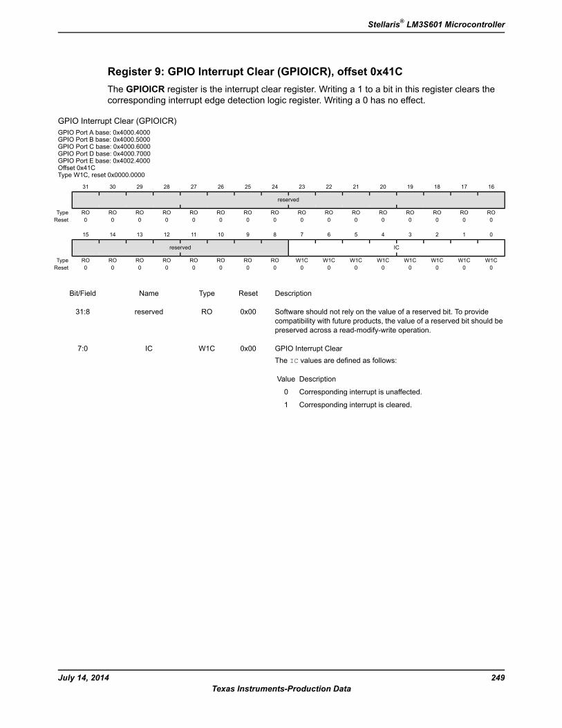
Register 9: GPIO Interrupt Clear (GPIOICR), offset 0x41CThe GPIOICR register is the interrupt clear register. Writing a 1 to a bit in this register clears thecorresponding interrupt edge detection logic register. Writing a 0 has no effect.
GPIO Interrupt Clear (GPIOICR)GPIO Port A base: 0x4000.4000GPIO Port B base: 0x4000.5000GPIO Port C base: 0x4000.6000GPIO Port D base: 0x4000.7000GPIO Port E base: 0x4002.4000Offset 0x41CType W1C, reset 0x0000.0000
16171819202122232425262728293031
reserved
ROROROROROROROROROROROROROROROROType0000000000000000Reset
0123456789101112131415
ICreserved
W1CW1CW1CW1CW1CW1CW1CW1CROROROROROROROROType0000000000000000Reset
DescriptionResetTypeNameBit/Field
Software should not rely on the value of a reserved bit. To providecompatibility with future products, the value of a reserved bit should bepreserved across a read-modify-write operation.
0x00ROreserved31:8
GPIO Interrupt ClearThe IC values are defined as follows:
DescriptionValue
Corresponding interrupt is unaffected.0
Corresponding interrupt is cleared.1
0x00W1CIC7:0
249July 14, 2014Texas Instruments-Production Data
Stellaris® LM3S601 Microcontroller
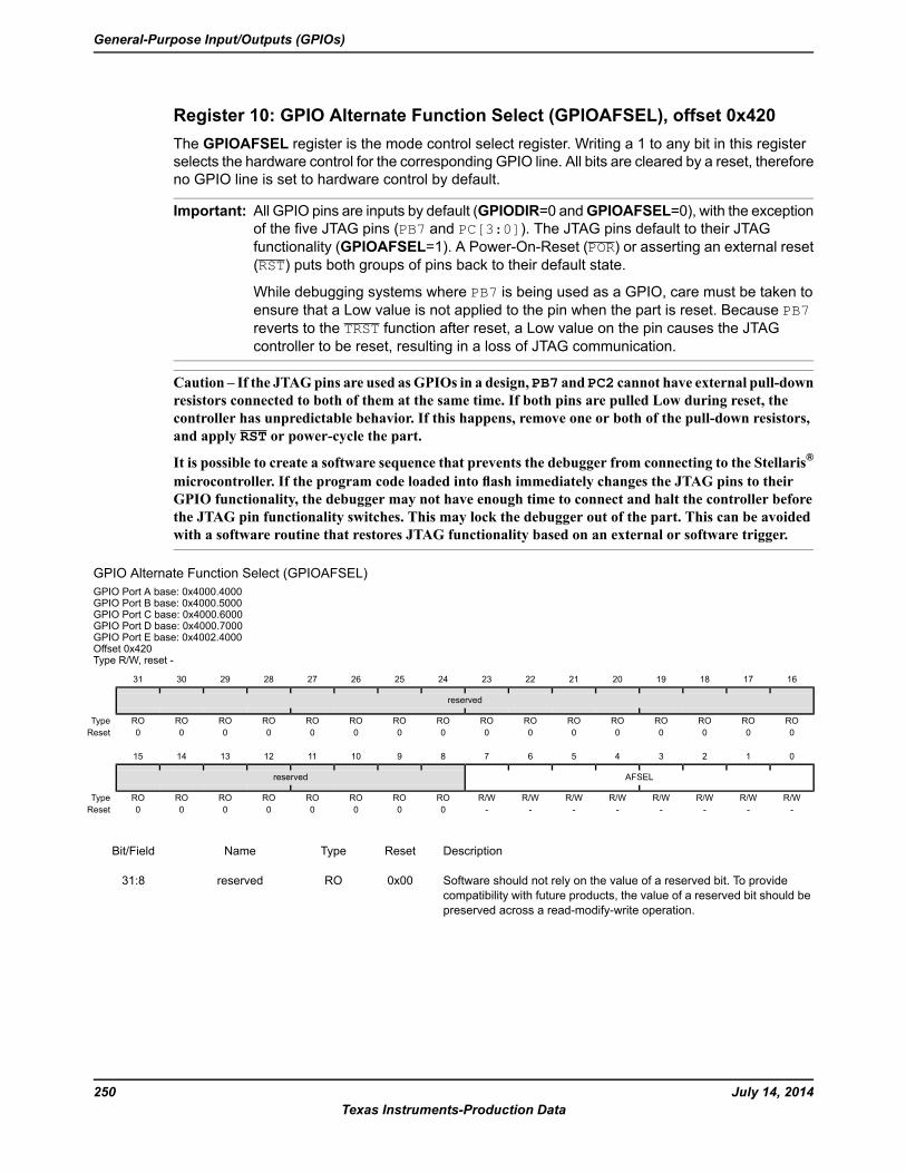
Register 10: GPIO Alternate Function Select (GPIOAFSEL), offset 0x420The GPIOAFSEL register is the mode control select register. Writing a 1 to any bit in this registerselects the hardware control for the corresponding GPIO line. All bits are cleared by a reset, thereforeno GPIO line is set to hardware control by default.
Important: All GPIO pins are inputs by default (GPIODIR=0 andGPIOAFSEL=0), with the exceptionof the five JTAG pins (PB7 and PC[3:0]). The JTAG pins default to their JTAGfunctionality (GPIOAFSEL=1). A Power-On-Reset (POR) or asserting an external reset(RST) puts both groups of pins back to their default state.
While debugging systems where PB7 is being used as a GPIO, care must be taken toensure that a Low value is not applied to the pin when the part is reset. Because PB7reverts to the TRST function after reset, a Low value on the pin causes the JTAGcontroller to be reset, resulting in a loss of JTAG communication.
Caution – If the JTAGpins are used asGPIOs in a design, PB7 and PC2 cannot have external pull-downresistors connected to both of them at the same time. If both pins are pulled Low during reset, thecontroller has unpredictable behavior. If this happens, remove one or both of the pull-down resistors,and apply RST or power-cycle the part.
It is possible to create a software sequence that prevents the debugger from connecting to the Stellaris®
microcontroller. If the program code loaded into flash immediately changes the JTAG pins to theirGPIO functionality, the debugger may not have enough time to connect and halt the controller beforethe JTAG pin functionality switches. This may lock the debugger out of the part. This can be avoidedwith a software routine that restores JTAG functionality based on an external or software trigger.
GPIO Alternate Function Select (GPIOAFSEL)GPIO Port A base: 0x4000.4000GPIO Port B base: 0x4000.5000GPIO Port C base: 0x4000.6000GPIO Port D base: 0x4000.7000GPIO Port E base: 0x4002.4000Offset 0x420Type R/W, reset -
16171819202122232425262728293031
reserved
ROROROROROROROROROROROROROROROROType0000000000000000Reset
0123456789101112131415
AFSELreserved
R/WR/WR/WR/WR/WR/WR/WR/WROROROROROROROROType--------00000000Reset
DescriptionResetTypeNameBit/Field
Software should not rely on the value of a reserved bit. To providecompatibility with future products, the value of a reserved bit should bepreserved across a read-modify-write operation.
0x00ROreserved31:8
July 14, 2014250Texas Instruments-Production Data
General-Purpose Input/Outputs (GPIOs)
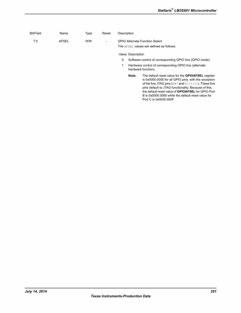
DescriptionResetTypeNameBit/Field
GPIO Alternate Function SelectThe AFSEL values are defined as follows:
DescriptionValue
Software control of corresponding GPIO line (GPIO mode).0
Hardware control of corresponding GPIO line (alternatehardware function).
1
Note: The default reset value for the GPIOAFSEL registeris 0x0000.0000 for all GPIO pins, with the exceptionof the five JTAG pins (PB7 and PC[3:0]). These fivepins default to JTAG functionality. Because of this,the default reset value ofGPIOAFSEL for GPIO PortB is 0x0000.0080 while the default reset value forPort C is 0x0000.000F.
-R/WAFSEL7:0
251July 14, 2014Texas Instruments-Production Data
Stellaris® LM3S601 Microcontroller
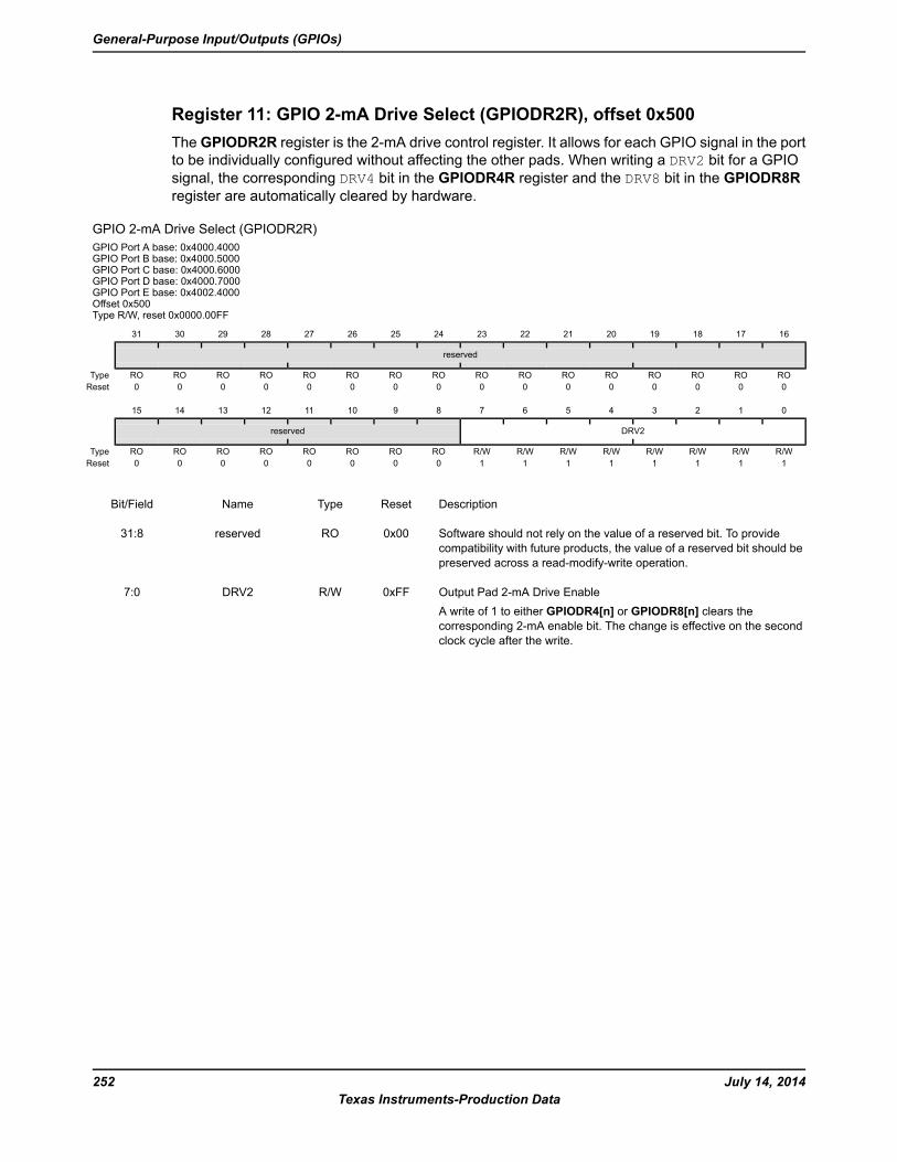
Register 11: GPIO 2-mA Drive Select (GPIODR2R), offset 0x500The GPIODR2R register is the 2-mA drive control register. It allows for each GPIO signal in the portto be individually configured without affecting the other pads. When writing a DRV2 bit for a GPIOsignal, the corresponding DRV4 bit in the GPIODR4R register and the DRV8 bit in the GPIODR8Rregister are automatically cleared by hardware.
GPIO 2-mA Drive Select (GPIODR2R)GPIO Port A base: 0x4000.4000GPIO Port B base: 0x4000.5000GPIO Port C base: 0x4000.6000GPIO Port D base: 0x4000.7000GPIO Port E base: 0x4002.4000Offset 0x500Type R/W, reset 0x0000.00FF
16171819202122232425262728293031
reserved
ROROROROROROROROROROROROROROROROType0000000000000000Reset
0123456789101112131415
DRV2reserved
R/WR/WR/WR/WR/WR/WR/WR/WROROROROROROROROType1111111100000000Reset
DescriptionResetTypeNameBit/Field
Software should not rely on the value of a reserved bit. To providecompatibility with future products, the value of a reserved bit should bepreserved across a read-modify-write operation.
0x00ROreserved31:8
Output Pad 2-mA Drive EnableA write of 1 to either GPIODR4[n] or GPIODR8[n] clears thecorresponding 2-mA enable bit. The change is effective on the secondclock cycle after the write.
0xFFR/WDRV27:0
July 14, 2014252Texas Instruments-Production Data
General-Purpose Input/Outputs (GPIOs)
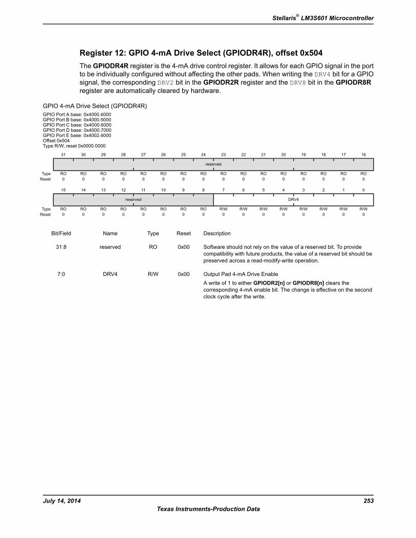
Register 12: GPIO 4-mA Drive Select (GPIODR4R), offset 0x504The GPIODR4R register is the 4-mA drive control register. It allows for each GPIO signal in the portto be individually configured without affecting the other pads. When writing the DRV4 bit for a GPIOsignal, the corresponding DRV2 bit in the GPIODR2R register and the DRV8 bit in the GPIODR8Rregister are automatically cleared by hardware.
GPIO 4-mA Drive Select (GPIODR4R)GPIO Port A base: 0x4000.4000GPIO Port B base: 0x4000.5000GPIO Port C base: 0x4000.6000GPIO Port D base: 0x4000.7000GPIO Port E base: 0x4002.4000Offset 0x504Type R/W, reset 0x0000.0000
16171819202122232425262728293031
reserved
ROROROROROROROROROROROROROROROROType0000000000000000Reset
0123456789101112131415
DRV4reserved
R/WR/WR/WR/WR/WR/WR/WR/WROROROROROROROROType0000000000000000Reset
DescriptionResetTypeNameBit/Field
Software should not rely on the value of a reserved bit. To providecompatibility with future products, the value of a reserved bit should bepreserved across a read-modify-write operation.
0x00ROreserved31:8
Output Pad 4-mA Drive EnableA write of 1 to either GPIODR2[n] or GPIODR8[n] clears thecorresponding 4-mA enable bit. The change is effective on the secondclock cycle after the write.
0x00R/WDRV47:0
253July 14, 2014Texas Instruments-Production Data
Stellaris® LM3S601 Microcontroller

Register 13: GPIO 8-mA Drive Select (GPIODR8R), offset 0x508The GPIODR8R register is the 8-mA drive control register. It allows for each GPIO signal in the portto be individually configured without affecting the other pads. When writing the DRV8 bit for a GPIOsignal, the corresponding DRV2 bit in the GPIODR2R register and the DRV4 bit in the GPIODR4Rregister are automatically cleared by hardware.
GPIO 8-mA Drive Select (GPIODR8R)GPIO Port A base: 0x4000.4000GPIO Port B base: 0x4000.5000GPIO Port C base: 0x4000.6000GPIO Port D base: 0x4000.7000GPIO Port E base: 0x4002.4000Offset 0x508Type R/W, reset 0x0000.0000
16171819202122232425262728293031
reserved
ROROROROROROROROROROROROROROROROType0000000000000000Reset
0123456789101112131415
DRV8reserved
R/WR/WR/WR/WR/WR/WR/WR/WROROROROROROROROType0000000000000000Reset
DescriptionResetTypeNameBit/Field
Software should not rely on the value of a reserved bit. To providecompatibility with future products, the value of a reserved bit should bepreserved across a read-modify-write operation.
0x00ROreserved31:8
Output Pad 8-mA Drive EnableA write of 1 to either GPIODR2[n] or GPIODR4[n] clears thecorresponding 8-mA enable bit. The change is effective on the secondclock cycle after the write.
0x00R/WDRV87:0
July 14, 2014254Texas Instruments-Production Data
General-Purpose Input/Outputs (GPIOs)
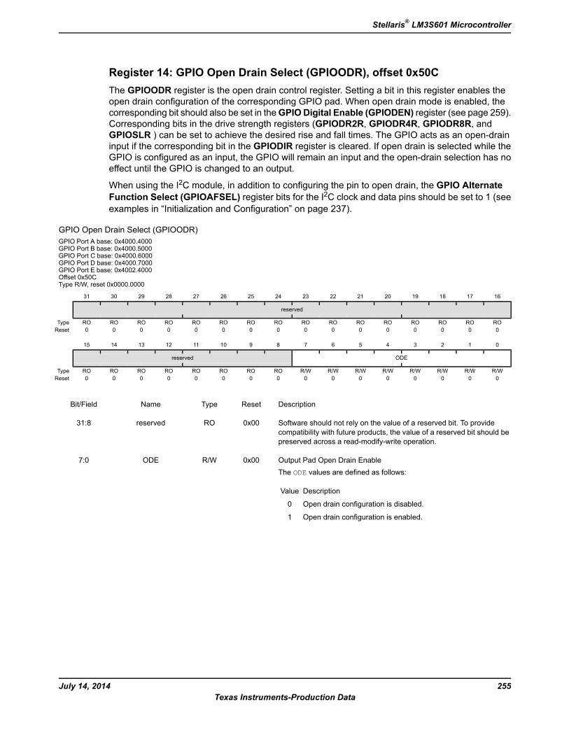
Register 14: GPIO Open Drain Select (GPIOODR), offset 0x50CThe GPIOODR register is the open drain control register. Setting a bit in this register enables theopen drain configuration of the corresponding GPIO pad. When open drain mode is enabled, thecorresponding bit should also be set in theGPIODigital Enable (GPIODEN) register (see page 259).Corresponding bits in the drive strength registers (GPIODR2R, GPIODR4R, GPIODR8R, andGPIOSLR ) can be set to achieve the desired rise and fall times. The GPIO acts as an open-draininput if the corresponding bit in the GPIODIR register is cleared. If open drain is selected while theGPIO is configured as an input, the GPIO will remain an input and the open-drain selection has noeffect until the GPIO is changed to an output.
When using the I2C module, in addition to configuring the pin to open drain, the GPIO AlternateFunction Select (GPIOAFSEL) register bits for the I2C clock and data pins should be set to 1 (seeexamples in “Initialization and Configuration” on page 237).
GPIO Open Drain Select (GPIOODR)GPIO Port A base: 0x4000.4000GPIO Port B base: 0x4000.5000GPIO Port C base: 0x4000.6000GPIO Port D base: 0x4000.7000GPIO Port E base: 0x4002.4000Offset 0x50CType R/W, reset 0x0000.0000
16171819202122232425262728293031
reserved
ROROROROROROROROROROROROROROROROType0000000000000000Reset
0123456789101112131415
ODEreserved
R/WR/WR/WR/WR/WR/WR/WR/WROROROROROROROROType0000000000000000Reset
DescriptionResetTypeNameBit/Field
Software should not rely on the value of a reserved bit. To providecompatibility with future products, the value of a reserved bit should bepreserved across a read-modify-write operation.
0x00ROreserved31:8
Output Pad Open Drain EnableThe ODE values are defined as follows:
DescriptionValue
Open drain configuration is disabled.0
Open drain configuration is enabled.1
0x00R/WODE7:0
255July 14, 2014Texas Instruments-Production Data
Stellaris® LM3S601 Microcontroller
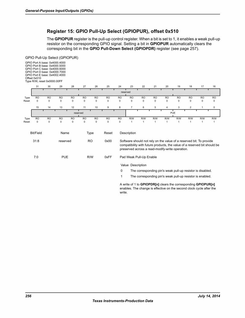
Register 15: GPIO Pull-Up Select (GPIOPUR), offset 0x510TheGPIOPUR register is the pull-up control register. When a bit is set to 1, it enables a weak pull-upresistor on the corresponding GPIO signal. Setting a bit in GPIOPUR automatically clears thecorresponding bit in the GPIO Pull-Down Select (GPIOPDR) register (see page 257).
GPIO Pull-Up Select (GPIOPUR)GPIO Port A base: 0x4000.4000GPIO Port B base: 0x4000.5000GPIO Port C base: 0x4000.6000GPIO Port D base: 0x4000.7000GPIO Port E base: 0x4002.4000Offset 0x510Type R/W, reset 0x0000.00FF
16171819202122232425262728293031
reserved
ROROROROROROROROROROROROROROROROType0000000000000000Reset
0123456789101112131415
PUEreserved
R/WR/WR/WR/WR/WR/WR/WR/WROROROROROROROROType1111111100000000Reset
DescriptionResetTypeNameBit/Field
Software should not rely on the value of a reserved bit. To providecompatibility with future products, the value of a reserved bit should bepreserved across a read-modify-write operation.
0x00ROreserved31:8
Pad Weak Pull-Up Enable
DescriptionValue
The corresponding pin's weak pull-up resistor is disabled.0
The corresponding pin's weak pull-up resistor is enabled.1
A write of 1 to GPIOPDR[n] clears the corresponding GPIOPUR[n]enables. The change is effective on the second clock cycle after thewrite.
0xFFR/WPUE7:0
July 14, 2014256Texas Instruments-Production Data
General-Purpose Input/Outputs (GPIOs)
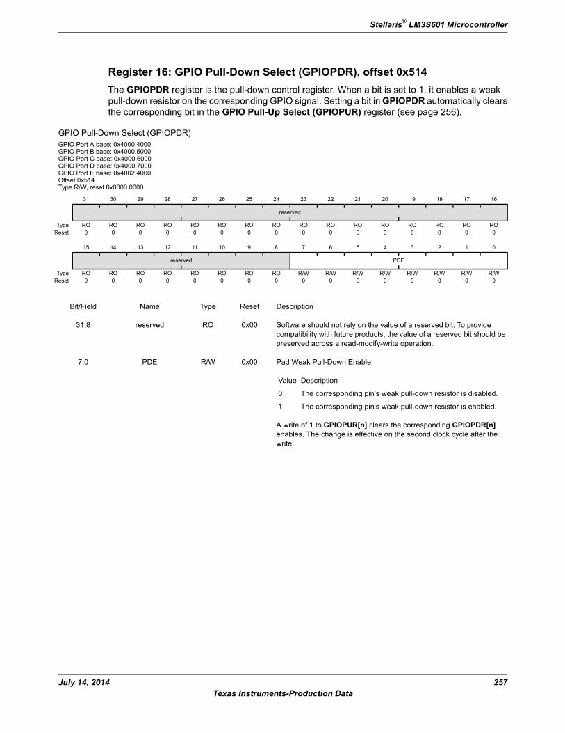
Register 16: GPIO Pull-Down Select (GPIOPDR), offset 0x514The GPIOPDR register is the pull-down control register. When a bit is set to 1, it enables a weakpull-down resistor on the corresponding GPIO signal. Setting a bit inGPIOPDR automatically clearsthe corresponding bit in the GPIO Pull-Up Select (GPIOPUR) register (see page 256).
GPIO Pull-Down Select (GPIOPDR)GPIO Port A base: 0x4000.4000GPIO Port B base: 0x4000.5000GPIO Port C base: 0x4000.6000GPIO Port D base: 0x4000.7000GPIO Port E base: 0x4002.4000Offset 0x514Type R/W, reset 0x0000.0000
16171819202122232425262728293031
reserved
ROROROROROROROROROROROROROROROROType0000000000000000Reset
0123456789101112131415
PDEreserved
R/WR/WR/WR/WR/WR/WR/WR/WROROROROROROROROType0000000000000000Reset
DescriptionResetTypeNameBit/Field
Software should not rely on the value of a reserved bit. To providecompatibility with future products, the value of a reserved bit should bepreserved across a read-modify-write operation.
0x00ROreserved31:8
Pad Weak Pull-Down Enable
DescriptionValue
The corresponding pin's weak pull-down resistor is disabled.0
The corresponding pin's weak pull-down resistor is enabled.1
A write of 1 to GPIOPUR[n] clears the corresponding GPIOPDR[n]enables. The change is effective on the second clock cycle after thewrite.
0x00R/WPDE7:0
257July 14, 2014Texas Instruments-Production Data
Stellaris® LM3S601 Microcontroller
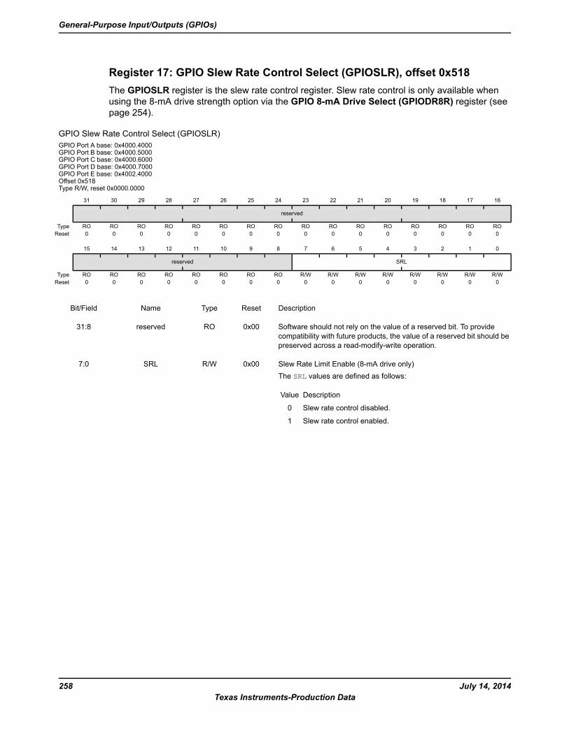
Register 17: GPIO Slew Rate Control Select (GPIOSLR), offset 0x518The GPIOSLR register is the slew rate control register. Slew rate control is only available whenusing the 8-mA drive strength option via the GPIO 8-mA Drive Select (GPIODR8R) register (seepage 254).
GPIO Slew Rate Control Select (GPIOSLR)GPIO Port A base: 0x4000.4000GPIO Port B base: 0x4000.5000GPIO Port C base: 0x4000.6000GPIO Port D base: 0x4000.7000GPIO Port E base: 0x4002.4000Offset 0x518Type R/W, reset 0x0000.0000
16171819202122232425262728293031
reserved
ROROROROROROROROROROROROROROROROType0000000000000000Reset
0123456789101112131415
SRLreserved
R/WR/WR/WR/WR/WR/WR/WR/WROROROROROROROROType0000000000000000Reset
DescriptionResetTypeNameBit/Field
Software should not rely on the value of a reserved bit. To providecompatibility with future products, the value of a reserved bit should bepreserved across a read-modify-write operation.
0x00ROreserved31:8
Slew Rate Limit Enable (8-mA drive only)The SRL values are defined as follows:
DescriptionValue
Slew rate control disabled.0
Slew rate control enabled.1
0x00R/WSRL7:0
July 14, 2014258Texas Instruments-Production Data
General-Purpose Input/Outputs (GPIOs)
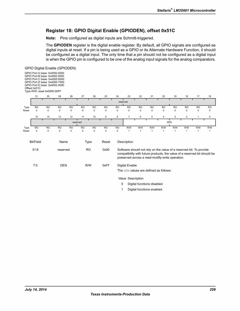
Register 18: GPIO Digital Enable (GPIODEN), offset 0x51CNote: Pins configured as digital inputs are Schmitt-triggered.
The GPIODEN register is the digital enable register. By default, all GPIO signals are configured asdigital inputs at reset. If a pin is being used as a GPIO or its Alternate Hardware Function, it shouldbe configured as a digital input. The only time that a pin should not be configured as a digital inputis when the GPIO pin is configured to be one of the analog input signals for the analog comparators.
GPIO Digital Enable (GPIODEN)GPIO Port A base: 0x4000.4000GPIO Port B base: 0x4000.5000GPIO Port C base: 0x4000.6000GPIO Port D base: 0x4000.7000GPIO Port E base: 0x4002.4000Offset 0x51CType R/W, reset 0x0000.00FF
16171819202122232425262728293031
reserved
ROROROROROROROROROROROROROROROROType0000000000000000Reset
0123456789101112131415
DENreserved
R/WR/WR/WR/WR/WR/WR/WR/WROROROROROROROROType1111111100000000Reset
DescriptionResetTypeNameBit/Field
Software should not rely on the value of a reserved bit. To providecompatibility with future products, the value of a reserved bit should bepreserved across a read-modify-write operation.
0x00ROreserved31:8
Digital EnableThe DEN values are defined as follows:
DescriptionValue
Digital functions disabled.0
Digital functions enabled.1
0xFFR/WDEN7:0
259July 14, 2014Texas Instruments-Production Data
Stellaris® LM3S601 Microcontroller
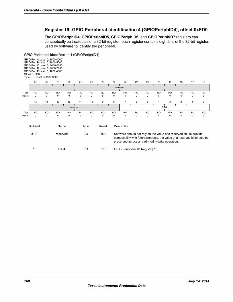
Register 19: GPIO Peripheral Identification 4 (GPIOPeriphID4), offset 0xFD0The GPIOPeriphID4, GPIOPeriphID5, GPIOPeriphID6, and GPIOPeriphID7 registers canconceptually be treated as one 32-bit register; each register contains eight bits of the 32-bit register,used by software to identify the peripheral.
GPIO Peripheral Identification 4 (GPIOPeriphID4)GPIO Port A base: 0x4000.4000GPIO Port B base: 0x4000.5000GPIO Port C base: 0x4000.6000GPIO Port D base: 0x4000.7000GPIO Port E base: 0x4002.4000Offset 0xFD0Type RO, reset 0x0000.0000
16171819202122232425262728293031
reserved
ROROROROROROROROROROROROROROROROType0000000000000000Reset
0123456789101112131415
PID4reserved
ROROROROROROROROROROROROROROROROType0000000000000000Reset
DescriptionResetTypeNameBit/Field
Software should not rely on the value of a reserved bit. To providecompatibility with future products, the value of a reserved bit should bepreserved across a read-modify-write operation.
0x00ROreserved31:8
GPIO Peripheral ID Register[7:0]0x00ROPID47:0
July 14, 2014260Texas Instruments-Production Data
General-Purpose Input/Outputs (GPIOs)

Register 20: GPIO Peripheral Identification 5 (GPIOPeriphID5), offset 0xFD4The GPIOPeriphID4, GPIOPeriphID5, GPIOPeriphID6, and GPIOPeriphID7 registers canconceptually be treated as one 32-bit register; each register contains eight bits of the 32-bit register,used by software to identify the peripheral.
GPIO Peripheral Identification 5 (GPIOPeriphID5)GPIO Port A base: 0x4000.4000GPIO Port B base: 0x4000.5000GPIO Port C base: 0x4000.6000GPIO Port D base: 0x4000.7000GPIO Port E base: 0x4002.4000Offset 0xFD4Type RO, reset 0x0000.0000
16171819202122232425262728293031
reserved
ROROROROROROROROROROROROROROROROType0000000000000000Reset
0123456789101112131415
PID5reserved
ROROROROROROROROROROROROROROROROType0000000000000000Reset
DescriptionResetTypeNameBit/Field
Software should not rely on the value of a reserved bit. To providecompatibility with future products, the value of a reserved bit should bepreserved across a read-modify-write operation.
0x00ROreserved31:8
GPIO Peripheral ID Register[15:8]0x00ROPID57:0
261July 14, 2014Texas Instruments-Production Data
Stellaris® LM3S601 Microcontroller

Register 21: GPIO Peripheral Identification 6 (GPIOPeriphID6), offset 0xFD8The GPIOPeriphID4, GPIOPeriphID5, GPIOPeriphID6, and GPIOPeriphID7 registers canconceptually be treated as one 32-bit register; each register contains eight bits of the 32-bit register,used by software to identify the peripheral.
GPIO Peripheral Identification 6 (GPIOPeriphID6)GPIO Port A base: 0x4000.4000GPIO Port B base: 0x4000.5000GPIO Port C base: 0x4000.6000GPIO Port D base: 0x4000.7000GPIO Port E base: 0x4002.4000Offset 0xFD8Type RO, reset 0x0000.0000
16171819202122232425262728293031
reserved
ROROROROROROROROROROROROROROROROType0000000000000000Reset
0123456789101112131415
PID6reserved
ROROROROROROROROROROROROROROROROType0000000000000000Reset
DescriptionResetTypeNameBit/Field
Software should not rely on the value of a reserved bit. To providecompatibility with future products, the value of a reserved bit should bepreserved across a read-modify-write operation.
0x00ROreserved31:8
GPIO Peripheral ID Register[23:16]0x00ROPID67:0
July 14, 2014262Texas Instruments-Production Data
General-Purpose Input/Outputs (GPIOs)
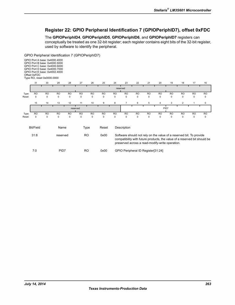
Register 22: GPIO Peripheral Identification 7 (GPIOPeriphID7), offset 0xFDCThe GPIOPeriphID4, GPIOPeriphID5, GPIOPeriphID6, and GPIOPeriphID7 registers canconceptually be treated as one 32-bit register; each register contains eight bits of the 32-bit register,used by software to identify the peripheral.
GPIO Peripheral Identification 7 (GPIOPeriphID7)GPIO Port A base: 0x4000.4000GPIO Port B base: 0x4000.5000GPIO Port C base: 0x4000.6000GPIO Port D base: 0x4000.7000GPIO Port E base: 0x4002.4000Offset 0xFDCType RO, reset 0x0000.0000
16171819202122232425262728293031
reserved
ROROROROROROROROROROROROROROROROType0000000000000000Reset
0123456789101112131415
PID7reserved
ROROROROROROROROROROROROROROROROType0000000000000000Reset
DescriptionResetTypeNameBit/Field
Software should not rely on the value of a reserved bit. To providecompatibility with future products, the value of a reserved bit should bepreserved across a read-modify-write operation.
0x00ROreserved31:8
GPIO Peripheral ID Register[31:24]0x00ROPID77:0
263July 14, 2014Texas Instruments-Production Data
Stellaris® LM3S601 Microcontroller

Register 23: GPIO Peripheral Identification 0 (GPIOPeriphID0), offset 0xFE0The GPIOPeriphID0, GPIOPeriphID1, GPIOPeriphID2, and GPIOPeriphID3 registers canconceptually be treated as one 32-bit register; each register contains eight bits of the 32-bit register,used by software to identify the peripheral.
GPIO Peripheral Identification 0 (GPIOPeriphID0)GPIO Port A base: 0x4000.4000GPIO Port B base: 0x4000.5000GPIO Port C base: 0x4000.6000GPIO Port D base: 0x4000.7000GPIO Port E base: 0x4002.4000Offset 0xFE0Type RO, reset 0x0000.0061
16171819202122232425262728293031
reserved
ROROROROROROROROROROROROROROROROType0000000000000000Reset
0123456789101112131415
PID0reserved
ROROROROROROROROROROROROROROROROType1000011000000000Reset
DescriptionResetTypeNameBit/Field
Software should not rely on the value of a reserved bit. To providecompatibility with future products, the value of a reserved bit should bepreserved across a read-modify-write operation.
0x00ROreserved31:8
GPIO Peripheral ID Register[7:0]Can be used by software to identify the presence of this peripheral.
0x61ROPID07:0
July 14, 2014264Texas Instruments-Production Data
General-Purpose Input/Outputs (GPIOs)
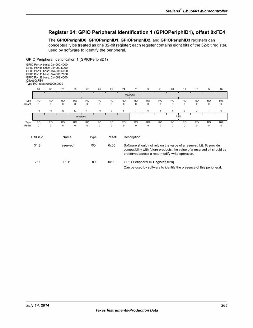
Register 24: GPIO Peripheral Identification 1 (GPIOPeriphID1), offset 0xFE4The GPIOPeriphID0, GPIOPeriphID1, GPIOPeriphID2, and GPIOPeriphID3 registers canconceptually be treated as one 32-bit register; each register contains eight bits of the 32-bit register,used by software to identify the peripheral.
GPIO Peripheral Identification 1 (GPIOPeriphID1)GPIO Port A base: 0x4000.4000GPIO Port B base: 0x4000.5000GPIO Port C base: 0x4000.6000GPIO Port D base: 0x4000.7000GPIO Port E base: 0x4002.4000Offset 0xFE4Type RO, reset 0x0000.0000
16171819202122232425262728293031
reserved
ROROROROROROROROROROROROROROROROType0000000000000000Reset
0123456789101112131415
PID1reserved
ROROROROROROROROROROROROROROROROType0000000000000000Reset
DescriptionResetTypeNameBit/Field
Software should not rely on the value of a reserved bit. To providecompatibility with future products, the value of a reserved bit should bepreserved across a read-modify-write operation.
0x00ROreserved31:8
GPIO Peripheral ID Register[15:8]Can be used by software to identify the presence of this peripheral.
0x00ROPID17:0
265July 14, 2014Texas Instruments-Production Data
Stellaris® LM3S601 Microcontroller
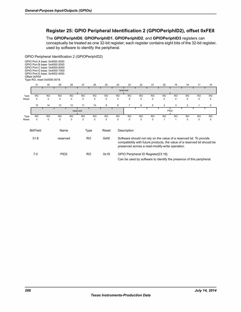
Register 25: GPIO Peripheral Identification 2 (GPIOPeriphID2), offset 0xFE8The GPIOPeriphID0, GPIOPeriphID1, GPIOPeriphID2, and GPIOPeriphID3 registers canconceptually be treated as one 32-bit register; each register contains eight bits of the 32-bit register,used by software to identify the peripheral.
GPIO Peripheral Identification 2 (GPIOPeriphID2)GPIO Port A base: 0x4000.4000GPIO Port B base: 0x4000.5000GPIO Port C base: 0x4000.6000GPIO Port D base: 0x4000.7000GPIO Port E base: 0x4002.4000Offset 0xFE8Type RO, reset 0x0000.0018
16171819202122232425262728293031
reserved
ROROROROROROROROROROROROROROROROType0000000000000000Reset
0123456789101112131415
PID2reserved
ROROROROROROROROROROROROROROROROType0001100000000000Reset
DescriptionResetTypeNameBit/Field
Software should not rely on the value of a reserved bit. To providecompatibility with future products, the value of a reserved bit should bepreserved across a read-modify-write operation.
0x00ROreserved31:8
GPIO Peripheral ID Register[23:16]Can be used by software to identify the presence of this peripheral.
0x18ROPID27:0
July 14, 2014266Texas Instruments-Production Data
General-Purpose Input/Outputs (GPIOs)

Register 26: GPIO Peripheral Identification 3 (GPIOPeriphID3), offset 0xFECThe GPIOPeriphID0, GPIOPeriphID1, GPIOPeriphID2, and GPIOPeriphID3 registers canconceptually be treated as one 32-bit register; each register contains eight bits of the 32-bit register,used by software to identify the peripheral.
GPIO Peripheral Identification 3 (GPIOPeriphID3)GPIO Port A base: 0x4000.4000GPIO Port B base: 0x4000.5000GPIO Port C base: 0x4000.6000GPIO Port D base: 0x4000.7000GPIO Port E base: 0x4002.4000Offset 0xFECType RO, reset 0x0000.0001
16171819202122232425262728293031
reserved
ROROROROROROROROROROROROROROROROType0000000000000000Reset
0123456789101112131415
PID3reserved
ROROROROROROROROROROROROROROROROType1000000000000000Reset
DescriptionResetTypeNameBit/Field
Software should not rely on the value of a reserved bit. To providecompatibility with future products, the value of a reserved bit should bepreserved across a read-modify-write operation.
0x00ROreserved31:8
GPIO Peripheral ID Register[31:24]Can be used by software to identify the presence of this peripheral.
0x01ROPID37:0
267July 14, 2014Texas Instruments-Production Data
Stellaris® LM3S601 Microcontroller

Register 27: GPIO PrimeCell Identification 0 (GPIOPCellID0), offset 0xFF0TheGPIOPCellID0,GPIOPCellID1,GPIOPCellID2, andGPIOPCellID3 registers are four 8-bit wideregisters, that can conceptually be treated as one 32-bit register. The register is used as a standardcross-peripheral identification system.
GPIO PrimeCell Identification 0 (GPIOPCellID0)GPIO Port A base: 0x4000.4000GPIO Port B base: 0x4000.5000GPIO Port C base: 0x4000.6000GPIO Port D base: 0x4000.7000GPIO Port E base: 0x4002.4000Offset 0xFF0Type RO, reset 0x0000.000D
16171819202122232425262728293031
reserved
ROROROROROROROROROROROROROROROROType0000000000000000Reset
0123456789101112131415
CID0reserved
ROROROROROROROROROROROROROROROROType1011000000000000Reset
DescriptionResetTypeNameBit/Field
Software should not rely on the value of a reserved bit. To providecompatibility with future products, the value of a reserved bit should bepreserved across a read-modify-write operation.
0x00ROreserved31:8
GPIO PrimeCell ID Register[7:0]Provides software a standard cross-peripheral identification system.
0x0DROCID07:0
July 14, 2014268Texas Instruments-Production Data
General-Purpose Input/Outputs (GPIOs)

Register 28: GPIO PrimeCell Identification 1 (GPIOPCellID1), offset 0xFF4TheGPIOPCellID0,GPIOPCellID1,GPIOPCellID2, andGPIOPCellID3 registers are four 8-bit wideregisters, that can conceptually be treated as one 32-bit register. The register is used as a standardcross-peripheral identification system.
GPIO PrimeCell Identification 1 (GPIOPCellID1)GPIO Port A base: 0x4000.4000GPIO Port B base: 0x4000.5000GPIO Port C base: 0x4000.6000GPIO Port D base: 0x4000.7000GPIO Port E base: 0x4002.4000Offset 0xFF4Type RO, reset 0x0000.00F0
16171819202122232425262728293031
reserved
ROROROROROROROROROROROROROROROROType0000000000000000Reset
0123456789101112131415
CID1reserved
ROROROROROROROROROROROROROROROROType0000111100000000Reset
DescriptionResetTypeNameBit/Field
Software should not rely on the value of a reserved bit. To providecompatibility with future products, the value of a reserved bit should bepreserved across a read-modify-write operation.
0x00ROreserved31:8
GPIO PrimeCell ID Register[15:8]Provides software a standard cross-peripheral identification system.
0xF0ROCID17:0
269July 14, 2014Texas Instruments-Production Data
Stellaris® LM3S601 Microcontroller

Register 29: GPIO PrimeCell Identification 2 (GPIOPCellID2), offset 0xFF8TheGPIOPCellID0,GPIOPCellID1,GPIOPCellID2, andGPIOPCellID3 registers are four 8-bit wideregisters, that can conceptually be treated as one 32-bit register. The register is used as a standardcross-peripheral identification system.
GPIO PrimeCell Identification 2 (GPIOPCellID2)GPIO Port A base: 0x4000.4000GPIO Port B base: 0x4000.5000GPIO Port C base: 0x4000.6000GPIO Port D base: 0x4000.7000GPIO Port E base: 0x4002.4000Offset 0xFF8Type RO, reset 0x0000.0005
16171819202122232425262728293031
reserved
ROROROROROROROROROROROROROROROROType0000000000000000Reset
0123456789101112131415
CID2reserved
ROROROROROROROROROROROROROROROROType1010000000000000Reset
DescriptionResetTypeNameBit/Field
Software should not rely on the value of a reserved bit. To providecompatibility with future products, the value of a reserved bit should bepreserved across a read-modify-write operation.
0x00ROreserved31:8
GPIO PrimeCell ID Register[23:16]Provides software a standard cross-peripheral identification system.
0x05ROCID27:0
July 14, 2014270Texas Instruments-Production Data
General-Purpose Input/Outputs (GPIOs)
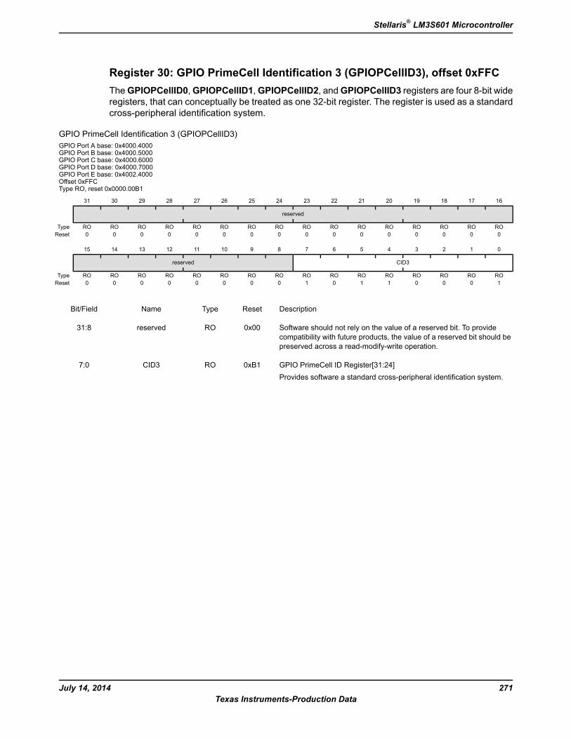
Register 30: GPIO PrimeCell Identification 3 (GPIOPCellID3), offset 0xFFCTheGPIOPCellID0,GPIOPCellID1,GPIOPCellID2, andGPIOPCellID3 registers are four 8-bit wideregisters, that can conceptually be treated as one 32-bit register. The register is used as a standardcross-peripheral identification system.
GPIO PrimeCell Identification 3 (GPIOPCellID3)GPIO Port A base: 0x4000.4000GPIO Port B base: 0x4000.5000GPIO Port C base: 0x4000.6000GPIO Port D base: 0x4000.7000GPIO Port E base: 0x4002.4000Offset 0xFFCType RO, reset 0x0000.00B1
16171819202122232425262728293031
reserved
ROROROROROROROROROROROROROROROROType0000000000000000Reset
0123456789101112131415
CID3reserved
ROROROROROROROROROROROROROROROROType1000110100000000Reset
DescriptionResetTypeNameBit/Field
Software should not rely on the value of a reserved bit. To providecompatibility with future products, the value of a reserved bit should bepreserved across a read-modify-write operation.
0x00ROreserved31:8
GPIO PrimeCell ID Register[31:24]Provides software a standard cross-peripheral identification system.
0xB1ROCID37:0
271July 14, 2014Texas Instruments-Production Data
Stellaris® LM3S601 Microcontroller
8 General-Purpose TimersProgrammable timers can be used to count or time external events that drive the Timer input pins.The Stellaris® General-Purpose Timer Module (GPTM) contains three GPTM blocks (Timer0, Timer1,and Timer 2). Each GPTM block provides two 16-bit timers/counters (referred to as TimerA andTimerB) that can be configured to operate independently as timers or event counters, or configuredto operate as one 32-bit timer or one 32-bit Real-Time Clock (RTC).
The GPT Module is one timing resource available on the Stellaris microcontrollers. Other timerresources include the System Timer (SysTick) (see 85) and the PWM timer in the PWM module(see “PWM Timer” on page 462).
The General-Purpose Timers provide the following features:
Three General-Purpose Timer Modules (GPTM), each of which provides two 16-bittimers/counters. Each GPTM can be configured to operate independently:
– As a single 32-bit timer
– As one 32-bit Real-Time Clock (RTC) to event capture
– For Pulse Width Modulation (PWM)
32-bit Timer modes
– Programmable one-shot timer
– Programmable periodic timer
– Real-Time Clock when using an external 32.768-KHz clock as the input
– User-enabled stalling when the controller asserts CPU Halt flag during debug
16-bit Timer modes
– General-purpose timer function with an 8-bit prescaler (for one-shot and periodic modes only)
– Programmable one-shot timer
– Programmable periodic timer
– User-enabled stalling when the controller asserts CPU Halt flag during debug
16-bit Input Capture modes
– Input edge count capture
– Input edge time capture
16-bit PWM mode
– Simple PWM mode with software-programmable output inversion of the PWM signal
July 14, 2014272Texas Instruments-Production Data
General-Purpose Timers
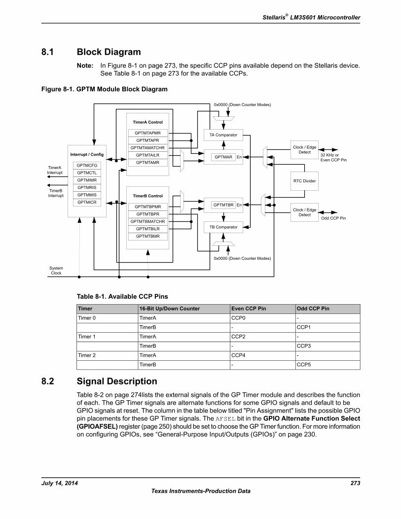
8.1 Block DiagramNote: In Figure 8-1 on page 273, the specific CCP pins available depend on the Stellaris device.
See Table 8-1 on page 273 for the available CCPs.
Figure 8-1. GPTM Module Block Diagram
TA Comparator
TB Comparator
GPTMTBR
GPTMAR
Clock / EdgeDetect
RTC Divider
Clock / EdgeDetect
TimerAInterrupt
TimerBInterrupt
SystemClock
0x0000 (Down Counter Modes)
0x0000 (Down Counter Modes)
32 KHz orEven CCP Pin
Odd CCP Pin
En
En
TimerA Control
GPTMTAPMR
GPTMTAILR
GPTMTAMATCHR
GPTMTAPR
GPTMTAMR
TimerB Control
GPTMTBPMR
GPTMTBILR
GPTMTBMATCHR
GPTMTBPR
GPTMTBMR
Interrupt / Config
GPTMCFG
GPTMRIS
GPTMICR
GPTMMIS
GPTMIMR
GPTMCTL
Table 8-1. Available CCP Pins
Odd CCP PinEven CCP Pin16-Bit Up/Down CounterTimer
-CCP0TimerATimer 0
CCP1-TimerB
-CCP2TimerATimer 1
CCP3-TimerB
-CCP4TimerATimer 2
CCP5-TimerB
8.2 Signal DescriptionTable 8-2 on page 274lists the external signals of the GP Timer module and describes the functionof each. The GP Timer signals are alternate functions for some GPIO signals and default to beGPIO signals at reset. The column in the table below titled "Pin Assignment" lists the possible GPIOpin placements for these GP Timer signals. The AFSEL bit in the GPIO Alternate Function Select(GPIOAFSEL) register (page 250) should be set to choose theGPTimer function. Formore informationon configuring GPIOs, see “General-Purpose Input/Outputs (GPIOs)” on page 230.
273July 14, 2014Texas Instruments-Production Data
Stellaris® LM3S601 Microcontroller
Table 8-2. General-Purpose Timers Signals (48QFP)
DescriptionBuffer TypeaPin TypePin NumberPin Name
Capture/Compare/PWM 0.TTLI/O45CCP0
Capture/Compare/PWM 1.TTLI/O3CCP1
Capture/Compare/PWM 2.TTLI/O46CCP2
Capture/Compare/PWM 3.TTLI/O2CCP3
Capture/Compare/PWM 4.TTLI/O4CCP4
Capture/Compare/PWM 5.TTLI/O1CCP5
a. The TTL designation indicates the pin has TTL-compatible voltage levels.
8.3 Functional DescriptionThe main components of each GPTM block are two free-running 16-bit up/down counters (referredto as TimerA and TimerB), two 16-bit match registers, two prescaler match registers, and two 16-bitload/initialization registers and their associated control functions. The exact functionality of eachGPTM is controlled by software and configured through the register interface.
Software configures the GPTM using theGPTMConfiguration (GPTMCFG) register (see page 284),the GPTM TimerA Mode (GPTMTAMR) register (see page 285), and the GPTM TimerB Mode(GPTMTBMR) register (see page 287). When in one of the 32-bit modes, the timer can only act asa 32-bit timer. However, when configured in 16-bit mode, the GPTM can have its two 16-bit timersconfigured in any combination of the 16-bit modes.
8.3.1 GPTM Reset ConditionsAfter reset has been applied to the GPTM module, the module is in an inactive state, and all controlregisters are cleared and in their default states. Counters TimerA and TimerB are initialized to0xFFFF, along with their corresponding load registers: the GPTM TimerA Interval Load(GPTMTAILR) register (see page 298) and theGPTMTimerB Interval Load (GPTMTBILR) register(see page 299). The prescale counters are initialized to 0x00: the GPTM TimerA Prescale(GPTMTAPR) register (see page 302) and theGPTMTimerB Prescale (GPTMTBPR) register (seepage 303).
8.3.2 32-Bit Timer Operating ModesThis section describes the three GPTM 32-bit timer modes (One-Shot, Periodic, and RTC) and theirconfiguration.
The GPTM is placed into 32-bit mode by writing a 0 (One-Shot/Periodic 32-bit timer mode) or a 1(RTCmode) to theGPTMConfiguration (GPTMCFG) register. In both configurations, certain GPTMregisters are concatenated to form pseudo 32-bit registers. These registers include:
GPTM TimerA Interval Load (GPTMTAILR) register [15:0], see page 298
GPTM TimerB Interval Load (GPTMTBILR) register [15:0], see page 299
GPTM TimerA (GPTMTAR) register [15:0], see page 306
GPTM TimerB (GPTMTBR) register [15:0], see page 307
In the 32-bit modes, the GPTM translates a 32-bit write access to GPTMTAILR into a write accessto both GPTMTAILR and GPTMTBILR. The resulting word ordering for such a write operation is:
GPTMTBILR[15:0]:GPTMTAILR[15:0]
July 14, 2014274Texas Instruments-Production Data
General-Purpose Timers
Likewise, a read access to GPTMTAR returns the value:
GPTMTBR[15:0]:GPTMTAR[15:0]
8.3.2.1 32-Bit One-Shot/Periodic Timer ModeIn 32-bit one-shot and periodic timer modes, the concatenated versions of the TimerA and TimerBregisters are configured as a 32-bit down-counter. The selection of one-shot or periodic mode isdetermined by the value written to the TAMR field of theGPTM TimerAMode (GPTMTAMR) register(see page 285), and there is no need to write to the GPTM TimerB Mode (GPTMTBMR) register.
When software writes the TAEN bit in the GPTM Control (GPTMCTL) register (see page 289), thetimer begins counting down from its preloaded value. Once the 0x0000.0000 state is reached, thetimer reloads its start value from the concatenated GPTMTAILR on the next cycle. If configured tobe a one-shot timer, the timer stops counting and clears the TAEN bit in the GPTMCTL register. Ifconfigured as a periodic timer, it continues counting.
In addition to reloading the count value, the GPTM generates interrupts and triggers when it reachesthe 0x000.0000 state. The GPTM sets the TATORIS bit in the GPTM Raw Interrupt Status(GPTMRIS) register (see page 294), and holds it until it is cleared by writing the GPTM InterruptClear (GPTMICR) register (see page 296). If the time-out interrupt is enabled in theGPTM InterruptMask (GPTMIMR) register (see page 292), theGPTMalso sets the TATOMIS bit in theGPTMMaskedInterrupt Status (GPTMMIS) register (see page 295).
If software reloads theGPTMTAILR register while the counter is running, the counter loads the newvalue on the next clock cycle and continues counting from the new value.
If the TASTALL bit in the GPTMCTL register is set, the timer freezes counting while the processoris halted by the debugger. The timer resumes counting when the processor resumes execution.
8.3.2.2 32-Bit Real-Time Clock Timer ModeIn Real-Time Clock (RTC) mode, the concatenated versions of the TimerA and TimerB registersare configured as a 32-bit up-counter. When RTC mode is selected for the first time, the counter isloaded with a value of 0x0000.0001. All subsequent load values must be written to theGPTMTimerAMatch (GPTMTAMATCHR) register (see page 300) by the controller.
The input clock on an even CCP input is required to be 32.768 KHz in RTC mode. The clock signalis then divided down to a 1 Hz rate and is passed along to the input of the 32-bit counter.
When software writes the TAEN bit inthe GPTMCTL register, the counter starts counting up from itspreloaded value of 0x0000.0001. When the current count value matches the preloaded value in theGPTMTAMATCHR register, it rolls over to a value of 0x0000.0000 and continues counting untileither a hardware reset, or it is disabled by software (clearing the TAEN bit). When a match occurs,the GPTM asserts the RTCRIS bit in GPTMRIS. If the RTC interrupt is enabled in GPTMIMR, theGPTM also sets the RTCMIS bit in GPTMMIS and generates a controller interrupt. The status flagsare cleared by writing the RTCCINT bit in GPTMICR.
If the TASTALL and/or TBSTALL bits in the GPTMCTL register are set, the timer does not freeze ifthe RTCEN bit is set in GPTMCTL.
8.3.3 16-Bit Timer Operating ModesThe GPTM is placed into global 16-bit mode by writing a value of 0x4 to the GPTM Configuration(GPTMCFG) register (see page 284). This section describes each of the GPTM 16-bit modes ofoperation. TimerA and TimerB have identical modes, so a single description is given using an n toreference both.
275July 14, 2014Texas Instruments-Production Data
Stellaris® LM3S601 Microcontroller
8.3.3.1 16-Bit One-Shot/Periodic Timer ModeIn 16-bit one-shot and periodic timer modes, the timer is configured as a 16-bit down-counter withan optional 8-bit prescaler that effectively extends the counting range of the timer to 24 bits. Theselection of one-shot or periodic mode is determined by the value written to the TnMR field of theGPTMTnMR register. The optional prescaler is loaded into theGPTMTimern Prescale (GPTMTnPR)register.
When software writes the TnEN bit in the GPTMCTL register, the timer begins counting down fromits preloaded value. Once the 0x0000 state is reached, the timer reloads its start value fromGPTMTnILR andGPTMTnPR on the next cycle. If configured to be a one-shot timer, the timer stopscounting and clears the TnEN bit in the GPTMCTL register. If configured as a periodic timer, itcontinues counting.
In addition to reloading the count value, the timer generates interrupts and triggers when it reachesthe 0x0000 state. The GPTM sets the TnTORIS bit in the GPTMRIS register, and holds it until it iscleared by writing theGPTMICR register. If the time-out interrupt is enabled inGPTMIMR, the GPTMalso sets the TnTOMIS bit in GPTMISR and generates a controller interrupt.
If software reloads theGPTMTAILR register while the counter is running, the counter loads the newvalue on the next clock cycle and continues counting from the new value.
If the TnSTALL bit in the GPTMCTL register is set, the timer freezes counting while the processoris halted by the debugger. The timer resumes counting when the processor resumes execution.
The following example shows a variety of configurations for a 16-bit free running timer while usingthe prescaler. All values assume a 50-MHz clock with Tc=20 ns (clock period).
Table 8-3. 16-Bit Timer With Prescaler Configurations
UnitsMax Time#Clock (T c)aPrescale
mS1.3107100000000
mS2.6214200000001
mS3.9322300000010
------------------
mS332.922925411111101
mS334.233625511111110
mS335.544325611111111
a. Tc is the clock period.
8.3.3.2 16-Bit Input Edge Count ModeNote: For rising-edge detection, the input signal must be High for at least two system clock periods
following the rising edge. Similarly, for falling-edge detection, the input signal must be Lowfor at least two system clock periods following the falling edge. Based on this criteria, themaximum input frequency for edge detection is 1/4 of the system frequency.
Note: The prescaler is not available in 16-Bit Input Edge Count mode.
In Edge Count mode, the timer is configured as a down-counter capable of capturing three typesof events: rising edge, falling edge, or both. To place the timer in Edge Count mode, the TnCMR bitof the GPTMTnMR register must be set to 0. The type of edge that the timer counts is determinedby the TnEVENT fields of the GPTMCTL register. During initialization, the GPTM Timern Match(GPTMTnMATCHR) register is configured so that the difference between the value in theGPTMTnILR register and the GPTMTnMATCHR register equals the number of edge events thatmust be counted.
July 14, 2014276Texas Instruments-Production Data
General-Purpose Timers
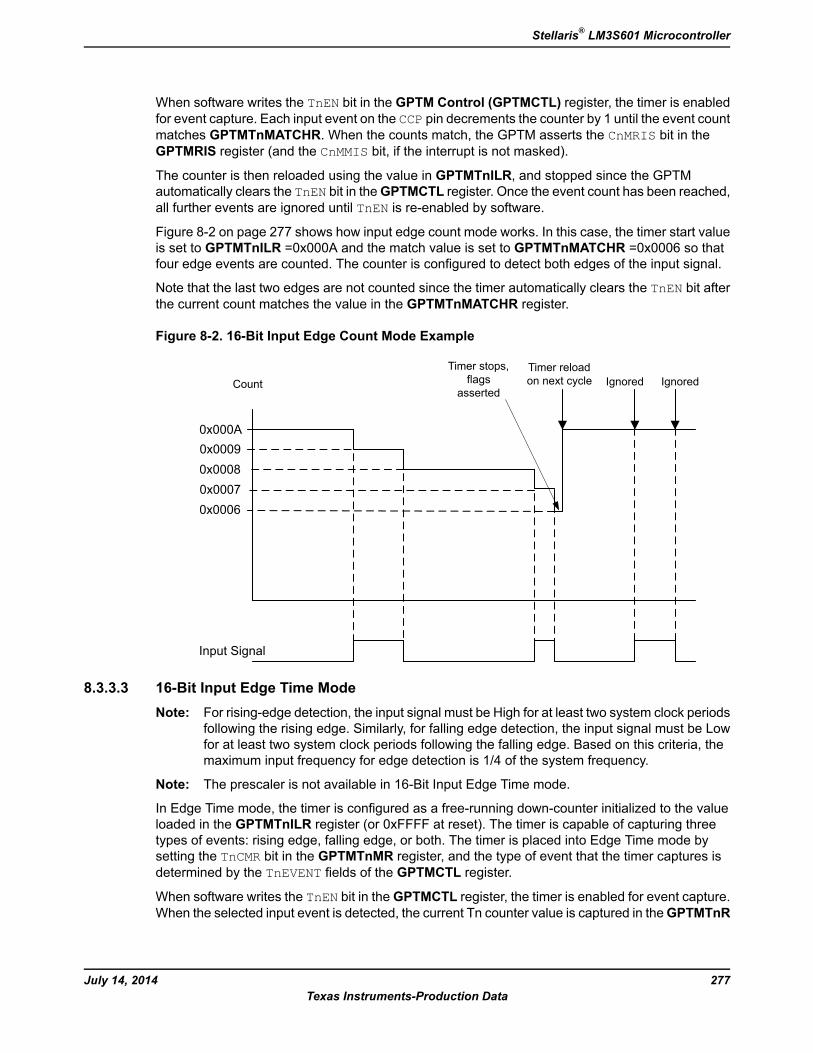
When software writes the TnEN bit in the GPTM Control (GPTMCTL) register, the timer is enabledfor event capture. Each input event on the CCP pin decrements the counter by 1 until the event countmatches GPTMTnMATCHR. When the counts match, the GPTM asserts the CnMRIS bit in theGPTMRIS register (and the CnMMIS bit, if the interrupt is not masked).
The counter is then reloaded using the value in GPTMTnILR, and stopped since the GPTMautomatically clears the TnEN bit in theGPTMCTL register. Once the event count has been reached,all further events are ignored until TnEN is re-enabled by software.
Figure 8-2 on page 277 shows how input edge count mode works. In this case, the timer start valueis set to GPTMTnILR =0x000A and the match value is set to GPTMTnMATCHR =0x0006 so thatfour edge events are counted. The counter is configured to detect both edges of the input signal.
Note that the last two edges are not counted since the timer automatically clears the TnEN bit afterthe current count matches the value in the GPTMTnMATCHR register.
Figure 8-2. 16-Bit Input Edge Count Mode Example
Input Signal
Timer stops,flags
asserted
Timer reloadon next cycle Ignored IgnoredCount
0x000A
0x00060x00070x00080x0009
8.3.3.3 16-Bit Input Edge Time ModeNote: For rising-edge detection, the input signal must be High for at least two system clock periods
following the rising edge. Similarly, for falling edge detection, the input signal must be Lowfor at least two system clock periods following the falling edge. Based on this criteria, themaximum input frequency for edge detection is 1/4 of the system frequency.
Note: The prescaler is not available in 16-Bit Input Edge Time mode.
In Edge Time mode, the timer is configured as a free-running down-counter initialized to the valueloaded in the GPTMTnILR register (or 0xFFFF at reset). The timer is capable of capturing threetypes of events: rising edge, falling edge, or both. The timer is placed into Edge Time mode bysetting the TnCMR bit in the GPTMTnMR register, and the type of event that the timer captures isdetermined by the TnEVENT fields of the GPTMCTL register.
When software writes the TnEN bit in theGPTMCTL register, the timer is enabled for event capture.When the selected input event is detected, the current Tn counter value is captured in theGPTMTnR
277July 14, 2014Texas Instruments-Production Data
Stellaris® LM3S601 Microcontroller
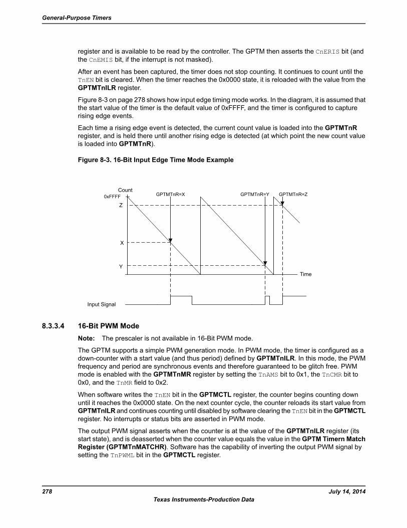
register and is available to be read by the controller. The GPTM then asserts the CnERIS bit (andthe CnEMIS bit, if the interrupt is not masked).
After an event has been captured, the timer does not stop counting. It continues to count until theTnEN bit is cleared. When the timer reaches the 0x0000 state, it is reloaded with the value from theGPTMTnILR register.
Figure 8-3 on page 278 shows how input edge timing mode works. In the diagram, it is assumed thatthe start value of the timer is the default value of 0xFFFF, and the timer is configured to capturerising edge events.
Each time a rising edge event is detected, the current count value is loaded into the GPTMTnRregister, and is held there until another rising edge is detected (at which point the new count valueis loaded into GPTMTnR).
Figure 8-3. 16-Bit Input Edge Time Mode Example
GPTMTnR=Y
Input Signal
Time
CountGPTMTnR=X GPTMTnR=Z
Z
X
Y
0xFFFF
8.3.3.4 16-Bit PWM ModeNote: The prescaler is not available in 16-Bit PWM mode.
The GPTM supports a simple PWM generation mode. In PWM mode, the timer is configured as adown-counter with a start value (and thus period) defined by GPTMTnILR. In this mode, the PWMfrequency and period are synchronous events and therefore guaranteed to be glitch free. PWMmode is enabled with the GPTMTnMR register by setting the TnAMS bit to 0x1, the TnCMR bit to0x0, and the TnMR field to 0x2.
When software writes the TnEN bit in the GPTMCTL register, the counter begins counting downuntil it reaches the 0x0000 state. On the next counter cycle, the counter reloads its start value fromGPTMTnILR and continues counting until disabled by software clearing the TnEN bit in theGPTMCTLregister. No interrupts or status bits are asserted in PWM mode.
The output PWM signal asserts when the counter is at the value of the GPTMTnILR register (itsstart state), and is deasserted when the counter value equals the value in theGPTM Timern MatchRegister (GPTMTnMATCHR). Software has the capability of inverting the output PWM signal bysetting the TnPWML bit in the GPTMCTL register.
July 14, 2014278Texas Instruments-Production Data
General-Purpose Timers
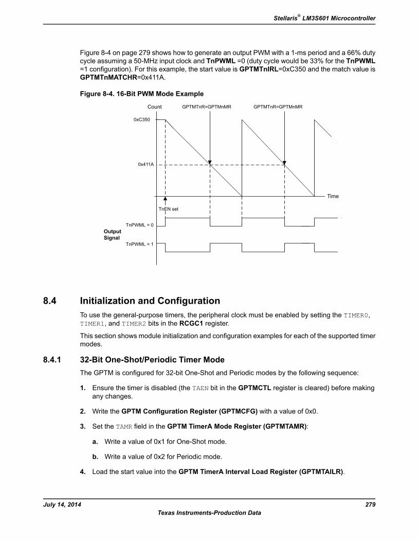
Figure 8-4 on page 279 shows how to generate an output PWM with a 1-ms period and a 66% dutycycle assuming a 50-MHz input clock and TnPWML =0 (duty cycle would be 33% for the TnPWML=1 configuration). For this example, the start value is GPTMTnIRL=0xC350 and the match value isGPTMTnMATCHR=0x411A.
Figure 8-4. 16-Bit PWM Mode Example
OutputSignal
Time
Count GPTMTnR=GPTMnMR GPTMTnR=GPTMnMR
0xC350
0x411A
TnPWML = 0
TnPWML = 1
TnEN set
8.4 Initialization and ConfigurationTo use the general-purpose timers, the peripheral clock must be enabled by setting the TIMER0,TIMER1, and TIMER2 bits in the RCGC1 register.
This section shows module initialization and configuration examples for each of the supported timermodes.
8.4.1 32-Bit One-Shot/Periodic Timer ModeThe GPTM is configured for 32-bit One-Shot and Periodic modes by the following sequence:
1. Ensure the timer is disabled (the TAEN bit in the GPTMCTL register is cleared) before makingany changes.
2. Write the GPTM Configuration Register (GPTMCFG) with a value of 0x0.
3. Set the TAMR field in the GPTM TimerA Mode Register (GPTMTAMR):
a. Write a value of 0x1 for One-Shot mode.
b. Write a value of 0x2 for Periodic mode.
4. Load the start value into the GPTM TimerA Interval Load Register (GPTMTAILR).
279July 14, 2014Texas Instruments-Production Data
Stellaris® LM3S601 Microcontroller
5. If interrupts are required, set the TATOIM bit in theGPTM Interrupt Mask Register (GPTMIMR).
6. Set the TAEN bit in the GPTMCTL register to enable the timer and start counting.
7. Poll the TATORIS bit in theGPTMRIS register or wait for the interrupt to be generated (if enabled).In both cases, the status flags are cleared by writing a 1 to the TATOCINT bit of the GPTMInterrupt Clear Register (GPTMICR).
In One-Shot mode, the timer stops counting after step 7 on page 280. To re-enable the timer, repeatthe sequence. A timer configured in Periodic mode does not stop counting after it times out.
8.4.2 32-Bit Real-Time Clock (RTC) ModeTo use the RTC mode, the timer must have a 32.768-KHz input signal on an even CCP input. Toenable the RTC feature, follow these steps:
1. Ensure the timer is disabled (the TAEN bit is cleared) before making any changes.
2. Write the GPTM Configuration Register (GPTMCFG) with a value of 0x1.
3. Write the desired match value to the GPTM TimerA Match Register (GPTMTAMATCHR).
4. Set/clear the RTCEN bit in the GPTM Control Register (GPTMCTL) as desired.
5. If interrupts are required, set the RTCIM bit in theGPTM Interrupt Mask Register (GPTMIMR).
6. Set the TAEN bit in the GPTMCTL register to enable the timer and start counting.
When the timer count equals the value in the GPTMTAMATCHR register, the GPTM asserts theRTCRIS bit in theGPTMRIS register and continues counting until Timer A is disabled or a hardwarereset. The interrupt is cleared by writing the RTCCINT bit in the GPTMICR register.
8.4.3 16-Bit One-Shot/Periodic Timer ModeA timer is configured for 16-bit One-Shot and Periodic modes by the following sequence:
1. Ensure the timer is disabled (the TnEN bit is cleared) before making any changes.
2. Write the GPTM Configuration Register (GPTMCFG) with a value of 0x4.
3. Set the TnMR field in the GPTM Timer Mode (GPTMTnMR) register:
a. Write a value of 0x1 for One-Shot mode.
b. Write a value of 0x2 for Periodic mode.
4. If a prescaler is to be used, write the prescale value to the GPTM Timern Prescale Register(GPTMTnPR).
5. Load the start value into the GPTM Timer Interval Load Register (GPTMTnILR).
6. If interrupts are required, set the TnTOIM bit in theGPTM Interrupt Mask Register (GPTMIMR).
7. Set the TnEN bit in the GPTM Control Register (GPTMCTL) to enable the timer and startcounting.
July 14, 2014280Texas Instruments-Production Data
General-Purpose Timers
8. Poll the TnTORIS bit in theGPTMRIS register or wait for the interrupt to be generated (if enabled).In both cases, the status flags are cleared by writing a 1 to the TnTOCINT bit of the GPTMInterrupt Clear Register (GPTMICR).
In One-Shot mode, the timer stops counting after step 8 on page 281. To re-enable the timer, repeatthe sequence. A timer configured in Periodic mode does not stop counting after it times out.
8.4.4 16-Bit Input Edge Count ModeA timer is configured to Input Edge Count mode by the following sequence:
1. Ensure the timer is disabled (the TnEN bit is cleared) before making any changes.
2. Write the GPTM Configuration (GPTMCFG) register with a value of 0x4.
3. In the GPTM Timer Mode (GPTMTnMR) register, write the TnCMR field to 0x0 and the TnMRfield to 0x3.
4. Configure the type of event(s) that the timer captures by writing the TnEVENT field of the GPTMControl (GPTMCTL) register.
5. Load the timer start value into the GPTM Timern Interval Load (GPTMTnILR) register.
6. Load the desired event count into the GPTM Timern Match (GPTMTnMATCHR) register.
7. If interrupts are required, set the CnMIM bit in the GPTM Interrupt Mask (GPTMIMR) register.
8. Set the TnEN bit in theGPTMCTL register to enable the timer and begin waiting for edge events.
9. Poll the CnMRIS bit in theGPTMRIS register or wait for the interrupt to be generated (if enabled).In both cases, the status flags are cleared by writing a 1 to the CnMCINT bit of the GPTMInterrupt Clear (GPTMICR) register.
In Input Edge Count Mode, the timer stops after the desired number of edge events has beendetected. To re-enable the timer, ensure that the TnEN bit is cleared and repeat step 4 on page 281through step 9 on page 281.
8.4.5 16-Bit Input Edge Timing ModeA timer is configured to Input Edge Timing mode by the following sequence:
1. Ensure the timer is disabled (the TnEN bit is cleared) before making any changes.
2. Write the GPTM Configuration (GPTMCFG) register with a value of 0x4.
3. In the GPTM Timer Mode (GPTMTnMR) register, write the TnCMR field to 0x1 and the TnMRfield to 0x3.
4. Configure the type of event that the timer captures by writing the TnEVENT field of the GPTMControl (GPTMCTL) register.
5. Load the timer start value into the GPTM Timern Interval Load (GPTMTnILR) register.
6. If interrupts are required, set the CnEIM bit in the GPTM Interrupt Mask (GPTMIMR) register.
7. Set the TnEN bit in theGPTMControl (GPTMCTL) register to enable the timer and start counting.
281July 14, 2014Texas Instruments-Production Data
Stellaris® LM3S601 Microcontroller
8. Poll the CnERIS bit in theGPTMRIS register or wait for the interrupt to be generated (if enabled).In both cases, the status flags are cleared by writing a 1 to the CnECINT bit of the GPTMInterrupt Clear (GPTMICR) register. The time at which the event happened can be obtainedby reading the GPTM Timern (GPTMTnR) register.
In Input Edge Timing mode, the timer continues running after an edge event has been detected,but the timer interval can be changed at any time by writing the GPTMTnILR register. The changetakes effect at the next cycle after the write.
8.4.6 16-Bit PWM ModeA timer is configured to PWM mode using the following sequence:
1. Ensure the timer is disabled (the TnEN bit is cleared) before making any changes.
2. Write the GPTM Configuration (GPTMCFG) register with a value of 0x4.
3. In the GPTM Timer Mode (GPTMTnMR) register, set the TnAMS bit to 0x1, the TnCMR bit to0x0, and the TnMR field to 0x2.
4. Configure the output state of the PWM signal (whether or not it is inverted) in the TnPWML fieldof the GPTM Control (GPTMCTL) register.
5. Load the timer start value into the GPTM Timern Interval Load (GPTMTnILR) register.
6. Load the GPTM Timern Match (GPTMTnMATCHR) register with the desired value.
7. Set the TnEN bit in the GPTM Control (GPTMCTL) register to enable the timer and begingeneration of the output PWM signal.
In PWM Timing mode, the timer continues running after the PWM signal has been generated. ThePWM period can be adjusted at any time by writing the GPTMTnILR register, and the change takeseffect at the next cycle after the write.
8.5 Register MapTable 8-4 on page 282 lists the GPTM registers. The offset listed is a hexadecimal increment to theregister’s address, relative to that timer’s base address:
Timer0: 0x4003.0000 Timer1: 0x4003.1000 Timer2: 0x4003.2000
Note that the Timer module clock must be enabled before the registers can be programmed (seepage 194). There must be a delay of 3 system clocks after the Timer module clock is enabled beforeany Timer module registers are accessed.
Table 8-4. Timers Register Map
SeepageDescriptionResetTypeNameOffset
284GPTM Configuration0x0000.0000R/WGPTMCFG0x000
285GPTM TimerA Mode0x0000.0000R/WGPTMTAMR0x004
July 14, 2014282Texas Instruments-Production Data
General-Purpose Timers
Table 8-4. Timers Register Map (continued)
SeepageDescriptionResetTypeNameOffset
287GPTM TimerB Mode0x0000.0000R/WGPTMTBMR0x008
289GPTM Control0x0000.0000R/WGPTMCTL0x00C
292GPTM Interrupt Mask0x0000.0000R/WGPTMIMR0x018
294GPTM Raw Interrupt Status0x0000.0000ROGPTMRIS0x01C
295GPTM Masked Interrupt Status0x0000.0000ROGPTMMIS0x020
296GPTM Interrupt Clear0x0000.0000W1CGPTMICR0x024
298GPTM TimerA Interval Load0xFFFF.FFFFR/WGPTMTAILR0x028
299GPTM TimerB Interval Load0x0000.FFFFR/WGPTMTBILR0x02C
300GPTM TimerA Match0xFFFF.FFFFR/WGPTMTAMATCHR0x030
301GPTM TimerB Match0x0000.FFFFR/WGPTMTBMATCHR0x034
302GPTM TimerA Prescale0x0000.0000R/WGPTMTAPR0x038
303GPTM TimerB Prescale0x0000.0000R/WGPTMTBPR0x03C
304GPTM TimerA Prescale Match0x0000.0000R/WGPTMTAPMR0x040
305GPTM TimerB Prescale Match0x0000.0000R/WGPTMTBPMR0x044
306GPTM TimerA0xFFFF.FFFFROGPTMTAR0x048
307GPTM TimerB0x0000.FFFFROGPTMTBR0x04C
8.6 Register DescriptionsThe remainder of this section lists and describes the GPTM registers, in numerical order by addressoffset.
283July 14, 2014Texas Instruments-Production Data
Stellaris® LM3S601 Microcontroller
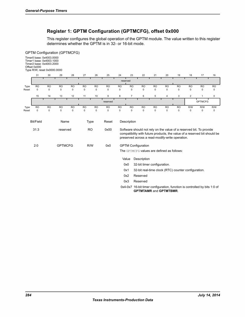
Register 1: GPTM Configuration (GPTMCFG), offset 0x000This register configures the global operation of the GPTM module. The value written to this registerdetermines whether the GPTM is in 32- or 16-bit mode.
GPTM Configuration (GPTMCFG)Timer0 base: 0x4003.0000Timer1 base: 0x4003.1000Timer2 base: 0x4003.2000Offset 0x000Type R/W, reset 0x0000.0000
16171819202122232425262728293031
reserved
ROROROROROROROROROROROROROROROROType0000000000000000Reset
0123456789101112131415
GPTMCFGreserved
R/WR/WR/WROROROROROROROROROROROROROType0000000000000000Reset
DescriptionResetTypeNameBit/Field
Software should not rely on the value of a reserved bit. To providecompatibility with future products, the value of a reserved bit should bepreserved across a read-modify-write operation.
0x00ROreserved31:3
GPTM ConfigurationThe GPTMCFG values are defined as follows:
DescriptionValue
32-bit timer configuration.0x0
32-bit real-time clock (RTC) counter configuration.0x1
Reserved0x2
Reserved0x3
16-bit timer configuration, function is controlled by bits 1:0 ofGPTMTAMR and GPTMTBMR.
0x4-0x7
0x0R/WGPTMCFG2:0
July 14, 2014284Texas Instruments-Production Data
General-Purpose Timers
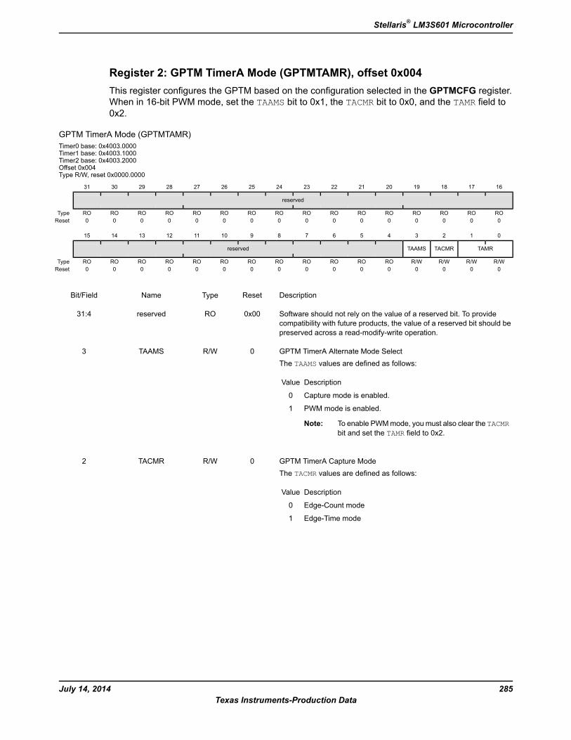
Register 2: GPTM TimerA Mode (GPTMTAMR), offset 0x004This register configures the GPTM based on the configuration selected in the GPTMCFG register.When in 16-bit PWM mode, set the TAAMS bit to 0x1, the TACMR bit to 0x0, and the TAMR field to0x2.
GPTM TimerA Mode (GPTMTAMR)Timer0 base: 0x4003.0000Timer1 base: 0x4003.1000Timer2 base: 0x4003.2000Offset 0x004Type R/W, reset 0x0000.0000
16171819202122232425262728293031
reserved
ROROROROROROROROROROROROROROROROType0000000000000000Reset
0123456789101112131415
TAMRTACMRTAAMSreserved
R/WR/WR/WR/WROROROROROROROROROROROROType0000000000000000Reset
DescriptionResetTypeNameBit/Field
Software should not rely on the value of a reserved bit. To providecompatibility with future products, the value of a reserved bit should bepreserved across a read-modify-write operation.
0x00ROreserved31:4
GPTM TimerA Alternate Mode SelectThe TAAMS values are defined as follows:
DescriptionValue
Capture mode is enabled.0
PWM mode is enabled.1
Note: To enable PWMmode, youmust also clear the TACMRbit and set the TAMR field to 0x2.
0R/WTAAMS3
GPTM TimerA Capture ModeThe TACMR values are defined as follows:
DescriptionValue
Edge-Count mode0
Edge-Time mode1
0R/WTACMR2
285July 14, 2014Texas Instruments-Production Data
Stellaris® LM3S601 Microcontroller
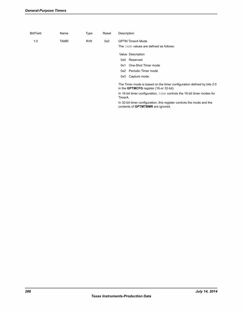
DescriptionResetTypeNameBit/Field
GPTM TimerA ModeThe TAMR values are defined as follows:
DescriptionValue
Reserved0x0
One-Shot Timer mode0x1
Periodic Timer mode0x2
Capture mode0x3
The Timer mode is based on the timer configuration defined by bits 2:0in the GPTMCFG register (16-or 32-bit).In 16-bit timer configuration, TAMR controls the 16-bit timer modes forTimerA.In 32-bit timer configuration, this register controls the mode and thecontents of GPTMTBMR are ignored.
0x0R/WTAMR1:0
July 14, 2014286Texas Instruments-Production Data
General-Purpose Timers

Register 3: GPTM TimerB Mode (GPTMTBMR), offset 0x008This register configures the GPTM based on the configuration selected in the GPTMCFG register.When in 16-bit PWM mode, set the TBAMS bit to 0x1, the TBCMR bit to 0x0, and the TBMR field to0x2.
GPTM TimerB Mode (GPTMTBMR)Timer0 base: 0x4003.0000Timer1 base: 0x4003.1000Timer2 base: 0x4003.2000Offset 0x008Type R/W, reset 0x0000.0000
16171819202122232425262728293031
reserved
ROROROROROROROROROROROROROROROROType0000000000000000Reset
0123456789101112131415
TBMRTBCMRTBAMSreserved
R/WR/WR/WR/WROROROROROROROROROROROROType0000000000000000Reset
DescriptionResetTypeNameBit/Field
Software should not rely on the value of a reserved bit. To providecompatibility with future products, the value of a reserved bit should bepreserved across a read-modify-write operation.
0x00ROreserved31:4
GPTM TimerB Alternate Mode SelectThe TBAMS values are defined as follows:
DescriptionValue
Capture mode is enabled.0
PWM mode is enabled.1
Note: To enable PWMmode, youmust also clear the TBCMRbit and set the TBMR field to 0x2.
0R/WTBAMS3
GPTM TimerB Capture ModeThe TBCMR values are defined as follows:
DescriptionValue
Edge-Count mode0
Edge-Time mode1
0R/WTBCMR2
287July 14, 2014Texas Instruments-Production Data
Stellaris® LM3S601 Microcontroller
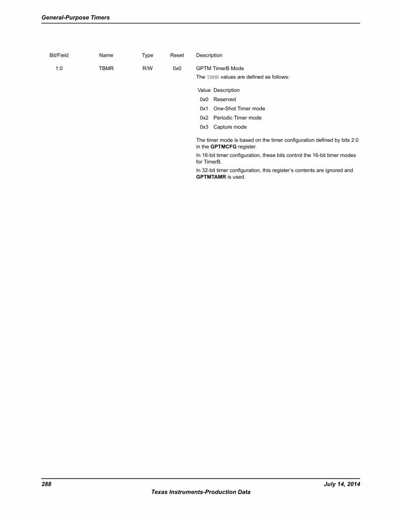
DescriptionResetTypeNameBit/Field
GPTM TimerB ModeThe TBMR values are defined as follows:
DescriptionValue
Reserved0x0
One-Shot Timer mode0x1
Periodic Timer mode0x2
Capture mode0x3
The timer mode is based on the timer configuration defined by bits 2:0in the GPTMCFG register.In 16-bit timer configuration, these bits control the 16-bit timer modesfor TimerB.In 32-bit timer configuration, this register’s contents are ignored andGPTMTAMR is used.
0x0R/WTBMR1:0
July 14, 2014288Texas Instruments-Production Data
General-Purpose Timers
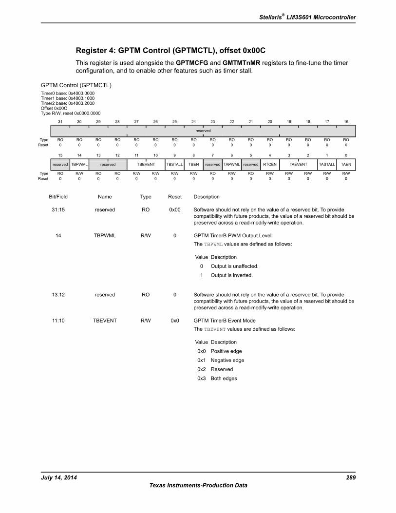
Register 4: GPTM Control (GPTMCTL), offset 0x00CThis register is used alongside the GPTMCFG and GMTMTnMR registers to fine-tune the timerconfiguration, and to enable other features such as timer stall.
GPTM Control (GPTMCTL)Timer0 base: 0x4003.0000Timer1 base: 0x4003.1000Timer2 base: 0x4003.2000Offset 0x00CType R/W, reset 0x0000.0000
16171819202122232425262728293031
reserved
ROROROROROROROROROROROROROROROROType0000000000000000Reset
0123456789101112131415
TAENTASTALLTAEVENTRTCENreservedTAPWMLreservedTBENTBSTALLTBEVENTreservedTBPWMLreserved
R/WR/WR/WR/WR/WROR/WROR/WR/WR/WR/WROROR/WROType0000000000000000Reset
DescriptionResetTypeNameBit/Field
Software should not rely on the value of a reserved bit. To providecompatibility with future products, the value of a reserved bit should bepreserved across a read-modify-write operation.
0x00ROreserved31:15
GPTM TimerB PWM Output LevelThe TBPWML values are defined as follows:
DescriptionValue
Output is unaffected.0
Output is inverted.1
0R/WTBPWML14
Software should not rely on the value of a reserved bit. To providecompatibility with future products, the value of a reserved bit should bepreserved across a read-modify-write operation.
0ROreserved13:12
GPTM TimerB Event ModeThe TBEVENT values are defined as follows:
DescriptionValue
Positive edge0x0
Negative edge0x1
Reserved0x2
Both edges0x3
0x0R/WTBEVENT11:10
289July 14, 2014Texas Instruments-Production Data
Stellaris® LM3S601 Microcontroller
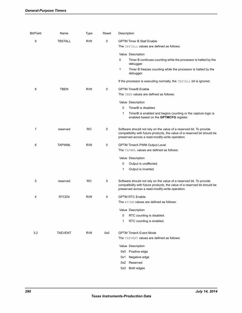
DescriptionResetTypeNameBit/Field
GPTM Timer B Stall EnableThe TBSTALL values are defined as follows:
DescriptionValue
Timer B continues counting while the processor is halted by thedebugger.
0
Timer B freezes counting while the processor is halted by thedebugger.
1
If the processor is executing normally, the TBSTALL bit is ignored.
0R/WTBSTALL9
GPTM TimerB EnableThe TBEN values are defined as follows:
DescriptionValue
TimerB is disabled.0
TimerB is enabled and begins counting or the capture logic isenabled based on the GPTMCFG register.
1
0R/WTBEN8
Software should not rely on the value of a reserved bit. To providecompatibility with future products, the value of a reserved bit should bepreserved across a read-modify-write operation.
0ROreserved7
GPTM TimerA PWM Output LevelThe TAPWML values are defined as follows:
DescriptionValue
Output is unaffected.0
Output is inverted.1
0R/WTAPWML6
Software should not rely on the value of a reserved bit. To providecompatibility with future products, the value of a reserved bit should bepreserved across a read-modify-write operation.
0ROreserved5
GPTM RTC EnableThe RTCEN values are defined as follows:
DescriptionValue
RTC counting is disabled.0
RTC counting is enabled.1
0R/WRTCEN4
GPTM TimerA Event ModeThe TAEVENT values are defined as follows:
DescriptionValue
Positive edge0x0
Negative edge0x1
Reserved0x2
Both edges0x3
0x0R/WTAEVENT3:2
July 14, 2014290Texas Instruments-Production Data
General-Purpose Timers
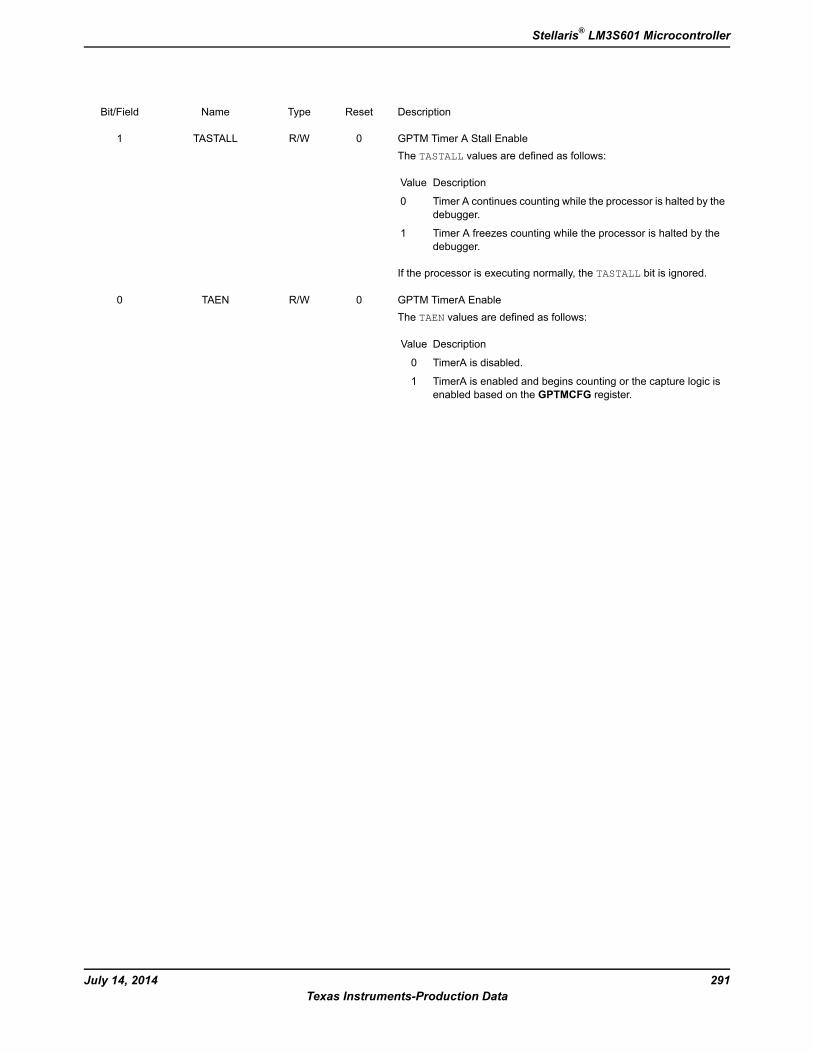
DescriptionResetTypeNameBit/Field
GPTM Timer A Stall EnableThe TASTALL values are defined as follows:
DescriptionValue
Timer A continues counting while the processor is halted by thedebugger.
0
Timer A freezes counting while the processor is halted by thedebugger.
1
If the processor is executing normally, the TASTALL bit is ignored.
0R/WTASTALL1
GPTM TimerA EnableThe TAEN values are defined as follows:
DescriptionValue
TimerA is disabled.0
TimerA is enabled and begins counting or the capture logic isenabled based on the GPTMCFG register.
1
0R/WTAEN0
291July 14, 2014Texas Instruments-Production Data
Stellaris® LM3S601 Microcontroller
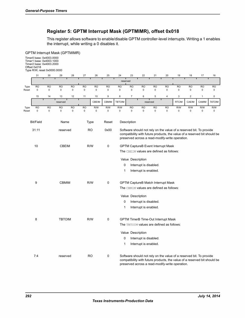
Register 5: GPTM Interrupt Mask (GPTMIMR), offset 0x018This register allows software to enable/disable GPTM controller-level interrupts. Writing a 1 enablesthe interrupt, while writing a 0 disables it.
GPTM Interrupt Mask (GPTMIMR)Timer0 base: 0x4003.0000Timer1 base: 0x4003.1000Timer2 base: 0x4003.2000Offset 0x018Type R/W, reset 0x0000.0000
16171819202122232425262728293031
reserved
ROROROROROROROROROROROROROROROROType0000000000000000Reset
0123456789101112131415
TATOIMCAMIMCAEIMRTCIMreservedTBTOIMCBMIMCBEIMreserved
R/WR/WR/WR/WROROROROR/WR/WR/WROROROROROType0000000000000000Reset
DescriptionResetTypeNameBit/Field
Software should not rely on the value of a reserved bit. To providecompatibility with future products, the value of a reserved bit should bepreserved across a read-modify-write operation.
0x00ROreserved31:11
GPTM CaptureB Event Interrupt MaskThe CBEIM values are defined as follows:
DescriptionValue
Interrupt is disabled.0
Interrupt is enabled.1
0R/WCBEIM10
GPTM CaptureB Match Interrupt MaskThe CBMIM values are defined as follows:
DescriptionValue
Interrupt is disabled.0
Interrupt is enabled.1
0R/WCBMIM9
GPTM TimerB Time-Out Interrupt MaskThe TBTOIM values are defined as follows:
DescriptionValue
Interrupt is disabled.0
Interrupt is enabled.1
0R/WTBTOIM8
Software should not rely on the value of a reserved bit. To providecompatibility with future products, the value of a reserved bit should bepreserved across a read-modify-write operation.
0ROreserved7:4
July 14, 2014292Texas Instruments-Production Data
General-Purpose Timers
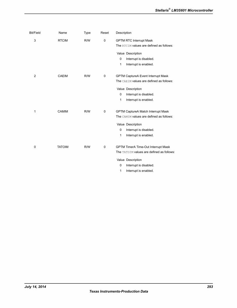
DescriptionResetTypeNameBit/Field
GPTM RTC Interrupt MaskThe RTCIM values are defined as follows:
DescriptionValue
Interrupt is disabled.0
Interrupt is enabled.1
0R/WRTCIM3
GPTM CaptureA Event Interrupt MaskThe CAEIM values are defined as follows:
DescriptionValue
Interrupt is disabled.0
Interrupt is enabled.1
0R/WCAEIM2
GPTM CaptureA Match Interrupt MaskThe CAMIM values are defined as follows:
DescriptionValue
Interrupt is disabled.0
Interrupt is enabled.1
0R/WCAMIM1
GPTM TimerA Time-Out Interrupt MaskThe TATOIM values are defined as follows:
DescriptionValue
Interrupt is disabled.0
Interrupt is enabled.1
0R/WTATOIM0
293July 14, 2014Texas Instruments-Production Data
Stellaris® LM3S601 Microcontroller
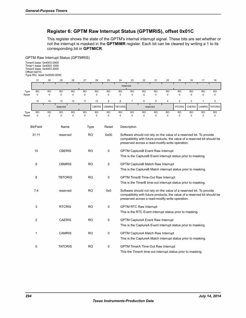
Register 6: GPTM Raw Interrupt Status (GPTMRIS), offset 0x01CThis register shows the state of the GPTM's internal interrupt signal. These bits are set whether ornot the interrupt is masked in the GPTMIMR register. Each bit can be cleared by writing a 1 to itscorresponding bit in GPTMICR.
GPTM Raw Interrupt Status (GPTMRIS)Timer0 base: 0x4003.0000Timer1 base: 0x4003.1000Timer2 base: 0x4003.2000Offset 0x01CType RO, reset 0x0000.0000
16171819202122232425262728293031
reserved
ROROROROROROROROROROROROROROROROType0000000000000000Reset
0123456789101112131415
TATORISCAMRISCAERISRTCRISreservedTBTORISCBMRISCBERISreserved
ROROROROROROROROROROROROROROROROType0000000000000000Reset
DescriptionResetTypeNameBit/Field
Software should not rely on the value of a reserved bit. To providecompatibility with future products, the value of a reserved bit should bepreserved across a read-modify-write operation.
0x00ROreserved31:11
GPTM CaptureB Event Raw InterruptThis is the CaptureB Event interrupt status prior to masking.
0ROCBERIS10
GPTM CaptureB Match Raw InterruptThis is the CaptureB Match interrupt status prior to masking.
0ROCBMRIS9
GPTM TimerB Time-Out Raw InterruptThis is the TimerB time-out interrupt status prior to masking.
0ROTBTORIS8
Software should not rely on the value of a reserved bit. To providecompatibility with future products, the value of a reserved bit should bepreserved across a read-modify-write operation.
0x0ROreserved7:4
GPTM RTC Raw InterruptThis is the RTC Event interrupt status prior to masking.
0RORTCRIS3
GPTM CaptureA Event Raw InterruptThis is the CaptureA Event interrupt status prior to masking.
0ROCAERIS2
GPTM CaptureA Match Raw InterruptThis is the CaptureA Match interrupt status prior to masking.
0ROCAMRIS1
GPTM TimerA Time-Out Raw InterruptThis the TimerA time-out interrupt status prior to masking.
0ROTATORIS0
July 14, 2014294Texas Instruments-Production Data
General-Purpose Timers
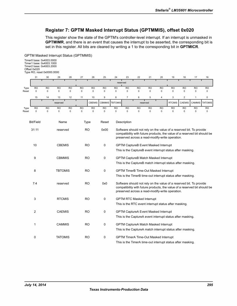
Register 7: GPTM Masked Interrupt Status (GPTMMIS), offset 0x020This register show the state of the GPTM's controller-level interrupt. If an interrupt is unmasked inGPTMIMR, and there is an event that causes the interrupt to be asserted, the corresponding bit isset in this register. All bits are cleared by writing a 1 to the corresponding bit in GPTMICR.
GPTM Masked Interrupt Status (GPTMMIS)Timer0 base: 0x4003.0000Timer1 base: 0x4003.1000Timer2 base: 0x4003.2000Offset 0x020Type RO, reset 0x0000.0000
16171819202122232425262728293031
reserved
ROROROROROROROROROROROROROROROROType0000000000000000Reset
0123456789101112131415
TATOMISCAMMISCAEMISRTCMISreservedTBTOMISCBMMISCBEMISreserved
ROROROROROROROROROROROROROROROROType0000000000000000Reset
DescriptionResetTypeNameBit/Field
Software should not rely on the value of a reserved bit. To providecompatibility with future products, the value of a reserved bit should bepreserved across a read-modify-write operation.
0x00ROreserved31:11
GPTM CaptureB Event Masked InterruptThis is the CaptureB event interrupt status after masking.
0ROCBEMIS10
GPTM CaptureB Match Masked InterruptThis is the CaptureB match interrupt status after masking.
0ROCBMMIS9
GPTM TimerB Time-Out Masked InterruptThis is the TimerB time-out interrupt status after masking.
0ROTBTOMIS8
Software should not rely on the value of a reserved bit. To providecompatibility with future products, the value of a reserved bit should bepreserved across a read-modify-write operation.
0x0ROreserved7:4
GPTM RTC Masked InterruptThis is the RTC event interrupt status after masking.
0RORTCMIS3
GPTM CaptureA Event Masked InterruptThis is the CaptureA event interrupt status after masking.
0ROCAEMIS2
GPTM CaptureA Match Masked InterruptThis is the CaptureA match interrupt status after masking.
0ROCAMMIS1
GPTM TimerA Time-Out Masked InterruptThis is the TimerA time-out interrupt status after masking.
0ROTATOMIS0
295July 14, 2014Texas Instruments-Production Data
Stellaris® LM3S601 Microcontroller
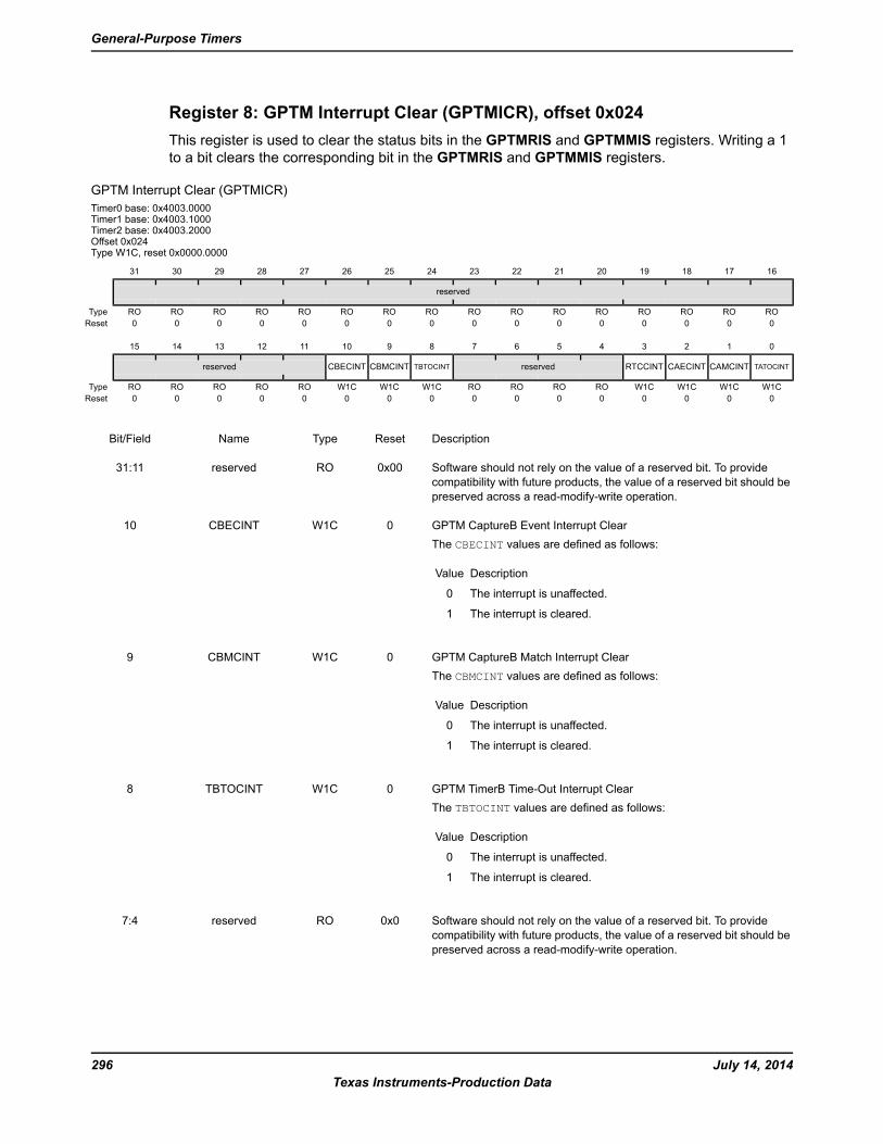
Register 8: GPTM Interrupt Clear (GPTMICR), offset 0x024This register is used to clear the status bits in the GPTMRIS and GPTMMIS registers. Writing a 1to a bit clears the corresponding bit in the GPTMRIS and GPTMMIS registers.
GPTM Interrupt Clear (GPTMICR)Timer0 base: 0x4003.0000Timer1 base: 0x4003.1000Timer2 base: 0x4003.2000Offset 0x024Type W1C, reset 0x0000.0000
16171819202122232425262728293031
reserved
ROROROROROROROROROROROROROROROROType0000000000000000Reset
0123456789101112131415
TATOCINTCAMCINTCAECINTRTCCINTreservedTBTOCINTCBMCINTCBECINTreserved
W1CW1CW1CW1CROROROROW1CW1CW1CROROROROROType0000000000000000Reset
DescriptionResetTypeNameBit/Field
Software should not rely on the value of a reserved bit. To providecompatibility with future products, the value of a reserved bit should bepreserved across a read-modify-write operation.
0x00ROreserved31:11
GPTM CaptureB Event Interrupt ClearThe CBECINT values are defined as follows:
DescriptionValue
The interrupt is unaffected.0
The interrupt is cleared.1
0W1CCBECINT10
GPTM CaptureB Match Interrupt ClearThe CBMCINT values are defined as follows:
DescriptionValue
The interrupt is unaffected.0
The interrupt is cleared.1
0W1CCBMCINT9
GPTM TimerB Time-Out Interrupt ClearThe TBTOCINT values are defined as follows:
DescriptionValue
The interrupt is unaffected.0
The interrupt is cleared.1
0W1CTBTOCINT8
Software should not rely on the value of a reserved bit. To providecompatibility with future products, the value of a reserved bit should bepreserved across a read-modify-write operation.
0x0ROreserved7:4
July 14, 2014296Texas Instruments-Production Data
General-Purpose Timers
DescriptionResetTypeNameBit/Field
GPTM RTC Interrupt ClearThe RTCCINT values are defined as follows:
DescriptionValue
The interrupt is unaffected.0
The interrupt is cleared.1
0W1CRTCCINT3
GPTM CaptureA Event Interrupt ClearThe CAECINT values are defined as follows:
DescriptionValue
The interrupt is unaffected.0
The interrupt is cleared.1
0W1CCAECINT2
GPTM CaptureA Match Interrupt ClearThe CAMCINT values are defined as follows:
DescriptionValue
The interrupt is unaffected.0
The interrupt is cleared.1
0W1CCAMCINT1
GPTM TimerA Time-Out Interrupt ClearThe TATOCINT values are defined as follows:
DescriptionValue
The interrupt is unaffected.0
The interrupt is cleared.1
0W1CTATOCINT0
297July 14, 2014Texas Instruments-Production Data
Stellaris® LM3S601 Microcontroller
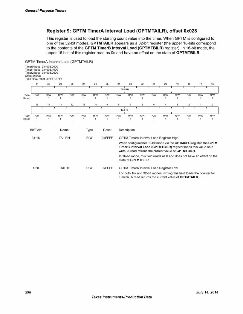
Register 9: GPTM TimerA Interval Load (GPTMTAILR), offset 0x028This register is used to load the starting count value into the timer. When GPTM is configured toone of the 32-bit modes, GPTMTAILR appears as a 32-bit register (the upper 16-bits correspondto the contents of the GPTM TimerB Interval Load (GPTMTBILR) register). In 16-bit mode, theupper 16 bits of this register read as 0s and have no effect on the state of GPTMTBILR.
GPTM TimerA Interval Load (GPTMTAILR)Timer0 base: 0x4003.0000Timer1 base: 0x4003.1000Timer2 base: 0x4003.2000Offset 0x028Type R/W, reset 0xFFFF.FFFF
16171819202122232425262728293031
TAILRH
R/WR/WR/WR/WR/WR/WR/WR/WR/WR/WR/WR/WR/WR/WR/WR/WType1111111111111111Reset
0123456789101112131415
TAILRL
R/WR/WR/WR/WR/WR/WR/WR/WR/WR/WR/WR/WR/WR/WR/WR/WType1111111111111111Reset
DescriptionResetTypeNameBit/Field
GPTM TimerA Interval Load Register HighWhen configured for 32-bit mode via theGPTMCFG register, theGPTMTimerB Interval Load (GPTMTBILR) register loads this value on awrite. A read returns the current value of GPTMTBILR.In 16-bit mode, this field reads as 0 and does not have an effect on thestate of GPTMTBILR.
0xFFFFR/WTAILRH31:16
GPTM TimerA Interval Load Register LowFor both 16- and 32-bit modes, writing this field loads the counter forTimerA. A read returns the current value of GPTMTAILR.
0xFFFFR/WTAILRL15:0
July 14, 2014298Texas Instruments-Production Data
General-Purpose Timers
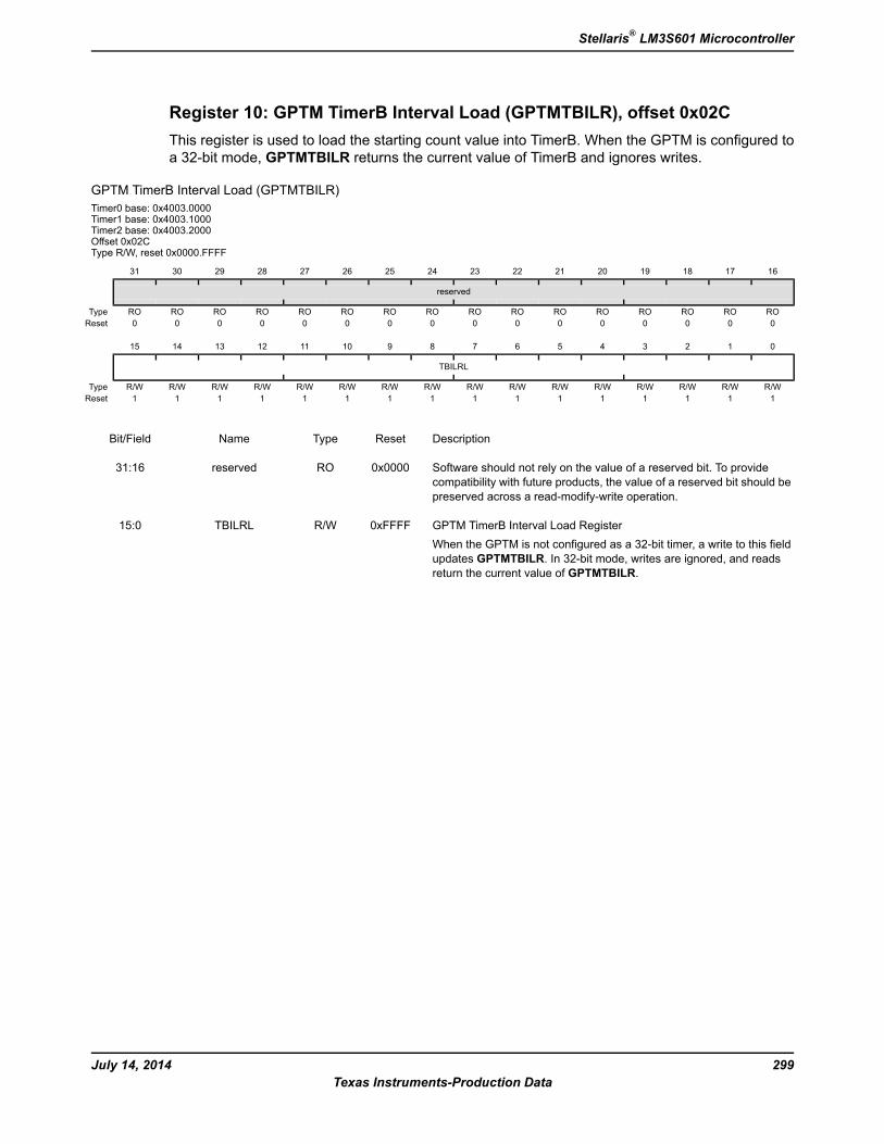
Register 10: GPTM TimerB Interval Load (GPTMTBILR), offset 0x02CThis register is used to load the starting count value into TimerB. When the GPTM is configured toa 32-bit mode, GPTMTBILR returns the current value of TimerB and ignores writes.
GPTM TimerB Interval Load (GPTMTBILR)Timer0 base: 0x4003.0000Timer1 base: 0x4003.1000Timer2 base: 0x4003.2000Offset 0x02CType R/W, reset 0x0000.FFFF
16171819202122232425262728293031
reserved
ROROROROROROROROROROROROROROROROType0000000000000000Reset
0123456789101112131415
TBILRL
R/WR/WR/WR/WR/WR/WR/WR/WR/WR/WR/WR/WR/WR/WR/WR/WType1111111111111111Reset
DescriptionResetTypeNameBit/Field
Software should not rely on the value of a reserved bit. To providecompatibility with future products, the value of a reserved bit should bepreserved across a read-modify-write operation.
0x0000ROreserved31:16
GPTM TimerB Interval Load RegisterWhen the GPTM is not configured as a 32-bit timer, a write to this fieldupdates GPTMTBILR. In 32-bit mode, writes are ignored, and readsreturn the current value of GPTMTBILR.
0xFFFFR/WTBILRL15:0
299July 14, 2014Texas Instruments-Production Data
Stellaris® LM3S601 Microcontroller
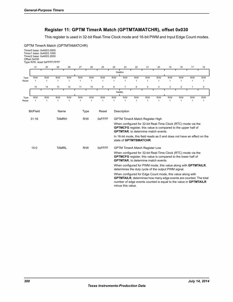
Register 11: GPTM TimerA Match (GPTMTAMATCHR), offset 0x030This register is used in 32-bit Real-Time Clock mode and 16-bit PWM and Input Edge Count modes.
GPTM TimerA Match (GPTMTAMATCHR)Timer0 base: 0x4003.0000Timer1 base: 0x4003.1000Timer2 base: 0x4003.2000Offset 0x030Type R/W, reset 0xFFFF.FFFF
16171819202122232425262728293031
TAMRH
R/WR/WR/WR/WR/WR/WR/WR/WR/WR/WR/WR/WR/WR/WR/WR/WType1111111111111111Reset
0123456789101112131415
TAMRL
R/WR/WR/WR/WR/WR/WR/WR/WR/WR/WR/WR/WR/WR/WR/WR/WType1111111111111111Reset
DescriptionResetTypeNameBit/Field
GPTM TimerA Match Register HighWhen configured for 32-bit Real-Time Clock (RTC) mode via theGPTMCFG register, this value is compared to the upper half ofGPTMTAR, to determine match events.In 16-bit mode, this field reads as 0 and does not have an effect on thestate of GPTMTBMATCHR.
0xFFFFR/WTAMRH31:16
GPTM TimerA Match Register LowWhen configured for 32-bit Real-Time Clock (RTC) mode via theGPTMCFG register, this value is compared to the lower half ofGPTMTAR, to determine match events.When configured for PWM mode, this value along with GPTMTAILR,determines the duty cycle of the output PWM signal.When configured for Edge Count mode, this value along withGPTMTAILR, determines howmany edge events are counted. The totalnumber of edge events counted is equal to the value in GPTMTAILRminus this value.
0xFFFFR/WTAMRL15:0
July 14, 2014300Texas Instruments-Production Data
General-Purpose Timers
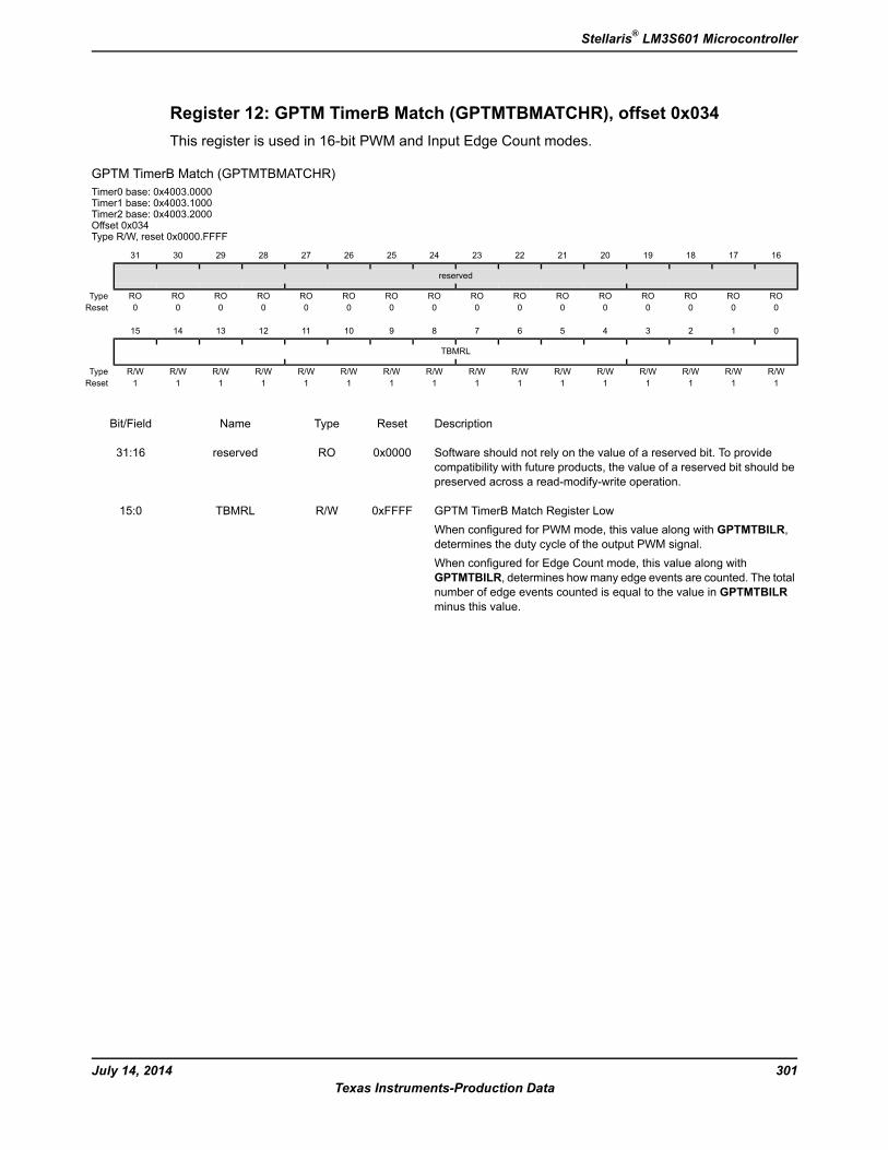
Register 12: GPTM TimerB Match (GPTMTBMATCHR), offset 0x034This register is used in 16-bit PWM and Input Edge Count modes.
GPTM TimerB Match (GPTMTBMATCHR)Timer0 base: 0x4003.0000Timer1 base: 0x4003.1000Timer2 base: 0x4003.2000Offset 0x034Type R/W, reset 0x0000.FFFF
16171819202122232425262728293031
reserved
ROROROROROROROROROROROROROROROROType0000000000000000Reset
0123456789101112131415
TBMRL
R/WR/WR/WR/WR/WR/WR/WR/WR/WR/WR/WR/WR/WR/WR/WR/WType1111111111111111Reset
DescriptionResetTypeNameBit/Field
Software should not rely on the value of a reserved bit. To providecompatibility with future products, the value of a reserved bit should bepreserved across a read-modify-write operation.
0x0000ROreserved31:16
GPTM TimerB Match Register LowWhen configured for PWM mode, this value along with GPTMTBILR,determines the duty cycle of the output PWM signal.When configured for Edge Count mode, this value along withGPTMTBILR, determines howmany edge events are counted. The totalnumber of edge events counted is equal to the value in GPTMTBILRminus this value.
0xFFFFR/WTBMRL15:0
301July 14, 2014Texas Instruments-Production Data
Stellaris® LM3S601 Microcontroller
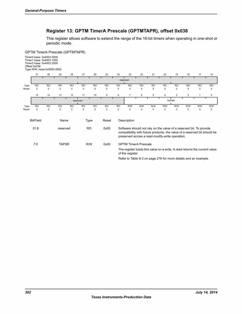
Register 13: GPTM TimerA Prescale (GPTMTAPR), offset 0x038This register allows software to extend the range of the 16-bit timers when operating in one-shot orperiodic mode.
GPTM TimerA Prescale (GPTMTAPR)Timer0 base: 0x4003.0000Timer1 base: 0x4003.1000Timer2 base: 0x4003.2000Offset 0x038Type R/W, reset 0x0000.0000
16171819202122232425262728293031
reserved
ROROROROROROROROROROROROROROROROType0000000000000000Reset
0123456789101112131415
TAPSRreserved
R/WR/WR/WR/WR/WR/WR/WR/WROROROROROROROROType0000000000000000Reset
DescriptionResetTypeNameBit/Field
Software should not rely on the value of a reserved bit. To providecompatibility with future products, the value of a reserved bit should bepreserved across a read-modify-write operation.
0x00ROreserved31:8
GPTM TimerA PrescaleThe register loads this value on a write. A read returns the current valueof the register.Refer to Table 8-3 on page 276 for more details and an example.
0x00R/WTAPSR7:0
July 14, 2014302Texas Instruments-Production Data
General-Purpose Timers
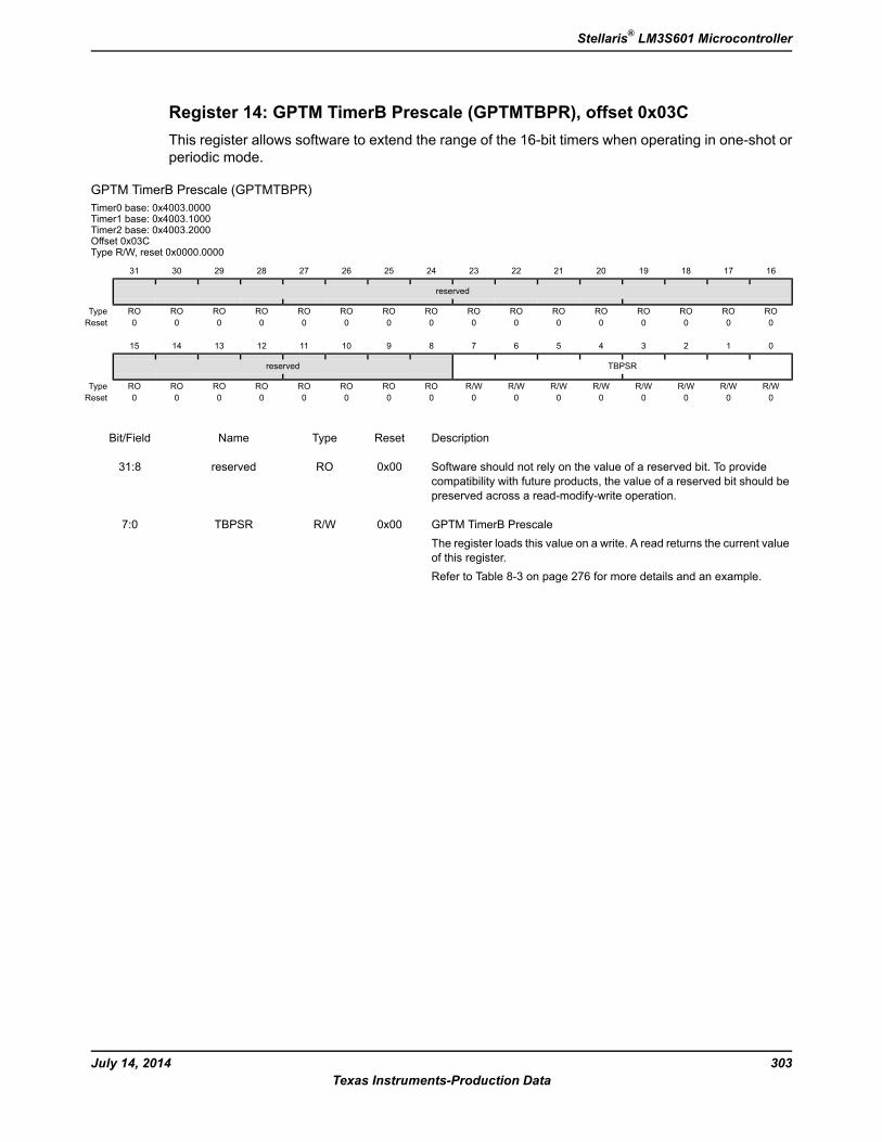
Register 14: GPTM TimerB Prescale (GPTMTBPR), offset 0x03CThis register allows software to extend the range of the 16-bit timers when operating in one-shot orperiodic mode.
GPTM TimerB Prescale (GPTMTBPR)Timer0 base: 0x4003.0000Timer1 base: 0x4003.1000Timer2 base: 0x4003.2000Offset 0x03CType R/W, reset 0x0000.0000
16171819202122232425262728293031
reserved
ROROROROROROROROROROROROROROROROType0000000000000000Reset
0123456789101112131415
TBPSRreserved
R/WR/WR/WR/WR/WR/WR/WR/WROROROROROROROROType0000000000000000Reset
DescriptionResetTypeNameBit/Field
Software should not rely on the value of a reserved bit. To providecompatibility with future products, the value of a reserved bit should bepreserved across a read-modify-write operation.
0x00ROreserved31:8
GPTM TimerB PrescaleThe register loads this value on a write. A read returns the current valueof this register.Refer to Table 8-3 on page 276 for more details and an example.
0x00R/WTBPSR7:0
303July 14, 2014Texas Instruments-Production Data
Stellaris® LM3S601 Microcontroller
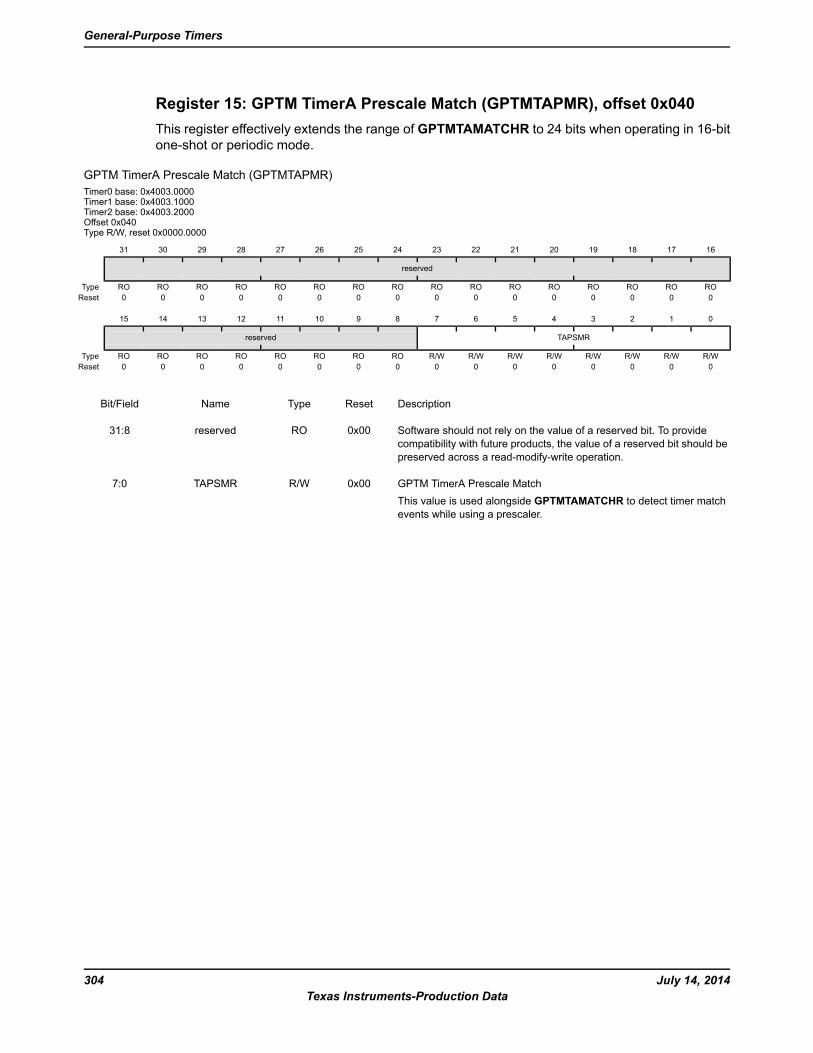
Register 15: GPTM TimerA Prescale Match (GPTMTAPMR), offset 0x040This register effectively extends the range of GPTMTAMATCHR to 24 bits when operating in 16-bitone-shot or periodic mode.
GPTM TimerA Prescale Match (GPTMTAPMR)Timer0 base: 0x4003.0000Timer1 base: 0x4003.1000Timer2 base: 0x4003.2000Offset 0x040Type R/W, reset 0x0000.0000
16171819202122232425262728293031
reserved
ROROROROROROROROROROROROROROROROType0000000000000000Reset
0123456789101112131415
TAPSMRreserved
R/WR/WR/WR/WR/WR/WR/WR/WROROROROROROROROType0000000000000000Reset
DescriptionResetTypeNameBit/Field
Software should not rely on the value of a reserved bit. To providecompatibility with future products, the value of a reserved bit should bepreserved across a read-modify-write operation.
0x00ROreserved31:8
GPTM TimerA Prescale MatchThis value is used alongside GPTMTAMATCHR to detect timer matchevents while using a prescaler.
0x00R/WTAPSMR7:0
July 14, 2014304Texas Instruments-Production Data
General-Purpose Timers
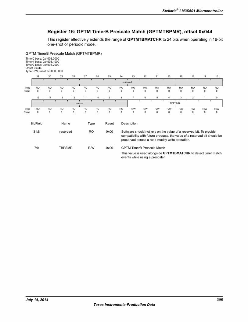
Register 16: GPTM TimerB Prescale Match (GPTMTBPMR), offset 0x044This register effectively extends the range of GPTMTBMATCHR to 24 bits when operating in 16-bitone-shot or periodic mode.
GPTM TimerB Prescale Match (GPTMTBPMR)Timer0 base: 0x4003.0000Timer1 base: 0x4003.1000Timer2 base: 0x4003.2000Offset 0x044Type R/W, reset 0x0000.0000
16171819202122232425262728293031
reserved
ROROROROROROROROROROROROROROROROType0000000000000000Reset
0123456789101112131415
TBPSMRreserved
R/WR/WR/WR/WR/WR/WR/WR/WROROROROROROROROType0000000000000000Reset
DescriptionResetTypeNameBit/Field
Software should not rely on the value of a reserved bit. To providecompatibility with future products, the value of a reserved bit should bepreserved across a read-modify-write operation.
0x00ROreserved31:8
GPTM TimerB Prescale MatchThis value is used alongside GPTMTBMATCHR to detect timer matchevents while using a prescaler.
0x00R/WTBPSMR7:0
305July 14, 2014Texas Instruments-Production Data
Stellaris® LM3S601 Microcontroller
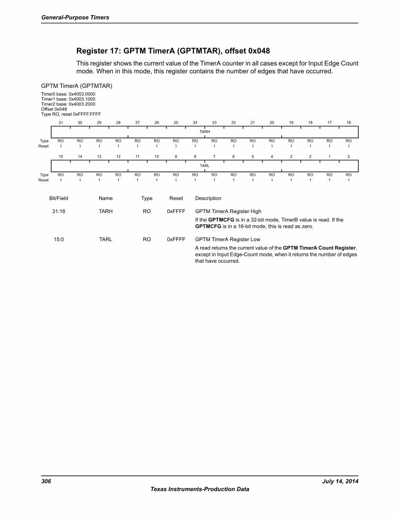
Register 17: GPTM TimerA (GPTMTAR), offset 0x048This register shows the current value of the TimerA counter in all cases except for Input Edge Countmode. When in this mode, this register contains the number of edges that have occurred.
GPTM TimerA (GPTMTAR)Timer0 base: 0x4003.0000Timer1 base: 0x4003.1000Timer2 base: 0x4003.2000Offset 0x048Type RO, reset 0xFFFF.FFFF
16171819202122232425262728293031
TARH
ROROROROROROROROROROROROROROROROType1111111111111111Reset
0123456789101112131415
TARL
ROROROROROROROROROROROROROROROROType1111111111111111Reset
DescriptionResetTypeNameBit/Field
GPTM TimerA Register HighIf the GPTMCFG is in a 32-bit mode, TimerB value is read. If theGPTMCFG is in a 16-bit mode, this is read as zero.
0xFFFFROTARH31:16
GPTM TimerA Register LowA read returns the current value of the GPTM TimerA Count Register,except in Input Edge-Count mode, when it returns the number of edgesthat have occurred.
0xFFFFROTARL15:0
July 14, 2014306Texas Instruments-Production Data
General-Purpose Timers
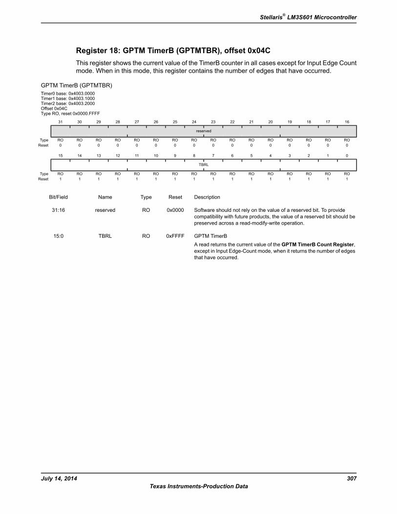
Register 18: GPTM TimerB (GPTMTBR), offset 0x04CThis register shows the current value of the TimerB counter in all cases except for Input Edge Countmode. When in this mode, this register contains the number of edges that have occurred.
GPTM TimerB (GPTMTBR)Timer0 base: 0x4003.0000Timer1 base: 0x4003.1000Timer2 base: 0x4003.2000Offset 0x04CType RO, reset 0x0000.FFFF
16171819202122232425262728293031
reserved
ROROROROROROROROROROROROROROROROType0000000000000000Reset
0123456789101112131415
TBRL
ROROROROROROROROROROROROROROROROType1111111111111111Reset
DescriptionResetTypeNameBit/Field
Software should not rely on the value of a reserved bit. To providecompatibility with future products, the value of a reserved bit should bepreserved across a read-modify-write operation.
0x0000ROreserved31:16
GPTM TimerBA read returns the current value of the GPTM TimerB Count Register,except in Input Edge-Count mode, when it returns the number of edgesthat have occurred.
0xFFFFROTBRL15:0
307July 14, 2014Texas Instruments-Production Data
Stellaris® LM3S601 Microcontroller
9 Watchdog TimerA watchdog timer can generate nonmaskable interrupts (NMIs) or a reset when a time-out value isreached. The watchdog timer is used to regain control when a system has failed due to a softwareerror or due to the failure of an external device to respond in the expected way.
The Stellaris® Watchdog Timer module has the following features:
32-bit down counter with a programmable load register
Separate watchdog clock with an enable
Programmable interrupt generation logic with interrupt masking
Lock register protection from runaway software
Reset generation logic with an enable/disable
User-enabled stalling when the controller asserts the CPU Halt flag during debug
TheWatchdog Timer can be configured to generate an interrupt to the controller on its first time-out,and to generate a reset signal on its second time-out. Once theWatchdog Timer has been configured,the lock register can be written to prevent the timer configuration from being inadvertently altered.
July 14, 2014308Texas Instruments-Production Data
Watchdog Timer
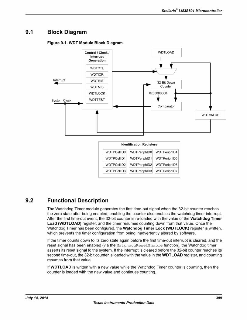
9.1 Block Diagram
Figure 9-1. WDT Module Block Diagram
Control / Clock /InterruptGeneration
WDTCTL
WDTICR
WDTRIS
WDTMIS
WDTLOCK
WDTTEST
WDTLOAD
WDTVALUE
Comparator
32-Bit DownCounter
0x00000000
Interrupt
System Clock
Identification Registers
WDTPCellID0 WDTPeriphID0 WDTPeriphID4
WDTPCellID1 WDTPeriphID1 WDTPeriphID5
WDTPCellID2 WDTPeriphID2 WDTPeriphID6
WDTPCellID3 WDTPeriphID3 WDTPeriphID7
9.2 Functional DescriptionThe Watchdog Timer module generates the first time-out signal when the 32-bit counter reachesthe zero state after being enabled; enabling the counter also enables the watchdog timer interrupt.After the first time-out event, the 32-bit counter is re-loaded with the value of theWatchdog TimerLoad (WDTLOAD) register, and the timer resumes counting down from that value. Once theWatchdog Timer has been configured, theWatchdog Timer Lock (WDTLOCK) register is written,which prevents the timer configuration from being inadvertently altered by software.
If the timer counts down to its zero state again before the first time-out interrupt is cleared, and thereset signal has been enabled (via the WatchdogResetEnable function), the Watchdog timerasserts its reset signal to the system. If the interrupt is cleared before the 32-bit counter reaches itssecond time-out, the 32-bit counter is loaded with the value in theWDTLOAD register, and countingresumes from that value.
IfWDTLOAD is written with a new value while the Watchdog Timer counter is counting, then thecounter is loaded with the new value and continues counting.
309July 14, 2014Texas Instruments-Production Data
Stellaris® LM3S601 Microcontroller
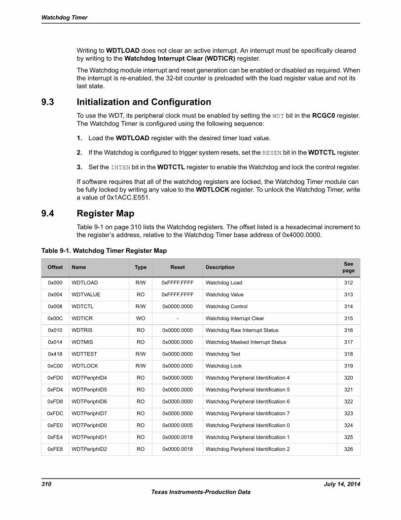
Writing toWDTLOAD does not clear an active interrupt. An interrupt must be specifically clearedby writing to theWatchdog Interrupt Clear (WDTICR) register.
TheWatchdog module interrupt and reset generation can be enabled or disabled as required. Whenthe interrupt is re-enabled, the 32-bit counter is preloaded with the load register value and not itslast state.
9.3 Initialization and ConfigurationTo use the WDT, its peripheral clock must be enabled by setting the WDT bit in the RCGC0 register.The Watchdog Timer is configured using the following sequence:
1. Load theWDTLOAD register with the desired timer load value.
2. If theWatchdog is configured to trigger system resets, set the RESEN bit in theWDTCTL register.
3. Set the INTEN bit in theWDTCTL register to enable the Watchdog and lock the control register.
If software requires that all of the watchdog registers are locked, the Watchdog Timer module canbe fully locked by writing any value to theWDTLOCK register. To unlock the Watchdog Timer, writea value of 0x1ACC.E551.
9.4 Register MapTable 9-1 on page 310 lists the Watchdog registers. The offset listed is a hexadecimal increment tothe register’s address, relative to the Watchdog Timer base address of 0x4000.0000.
Table 9-1. Watchdog Timer Register Map
SeepageDescriptionResetTypeNameOffset
312Watchdog Load0xFFFF.FFFFR/WWDTLOAD0x000
313Watchdog Value0xFFFF.FFFFROWDTVALUE0x004
314Watchdog Control0x0000.0000R/WWDTCTL0x008
315Watchdog Interrupt Clear-WOWDTICR0x00C
316Watchdog Raw Interrupt Status0x0000.0000ROWDTRIS0x010
317Watchdog Masked Interrupt Status0x0000.0000ROWDTMIS0x014
318Watchdog Test0x0000.0000R/WWDTTEST0x418
319Watchdog Lock0x0000.0000R/WWDTLOCK0xC00
320Watchdog Peripheral Identification 40x0000.0000ROWDTPeriphID40xFD0
321Watchdog Peripheral Identification 50x0000.0000ROWDTPeriphID50xFD4
322Watchdog Peripheral Identification 60x0000.0000ROWDTPeriphID60xFD8
323Watchdog Peripheral Identification 70x0000.0000ROWDTPeriphID70xFDC
324Watchdog Peripheral Identification 00x0000.0005ROWDTPeriphID00xFE0
325Watchdog Peripheral Identification 10x0000.0018ROWDTPeriphID10xFE4
326Watchdog Peripheral Identification 20x0000.0018ROWDTPeriphID20xFE8
July 14, 2014310Texas Instruments-Production Data
Watchdog Timer
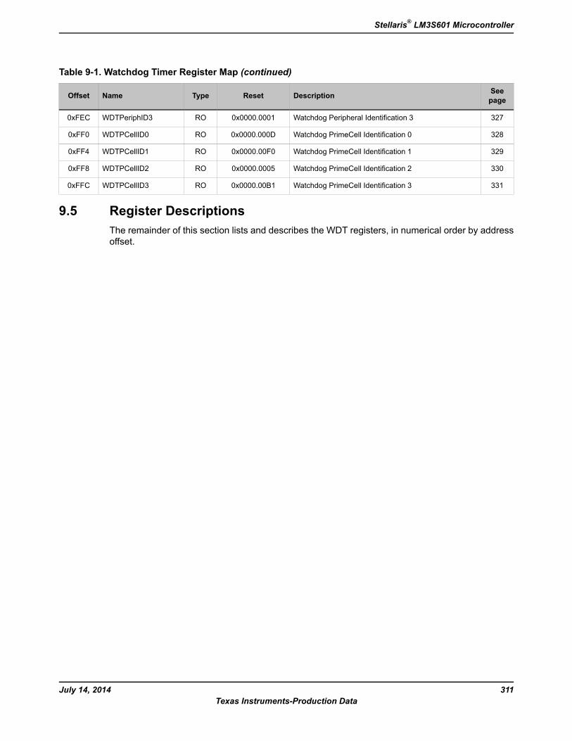
Table 9-1. Watchdog Timer Register Map (continued)
SeepageDescriptionResetTypeNameOffset
327Watchdog Peripheral Identification 30x0000.0001ROWDTPeriphID30xFEC
328Watchdog PrimeCell Identification 00x0000.000DROWDTPCellID00xFF0
329Watchdog PrimeCell Identification 10x0000.00F0ROWDTPCellID10xFF4
330Watchdog PrimeCell Identification 20x0000.0005ROWDTPCellID20xFF8
331Watchdog PrimeCell Identification 30x0000.00B1ROWDTPCellID30xFFC
9.5 Register DescriptionsThe remainder of this section lists and describes the WDT registers, in numerical order by addressoffset.
311July 14, 2014Texas Instruments-Production Data
Stellaris® LM3S601 Microcontroller
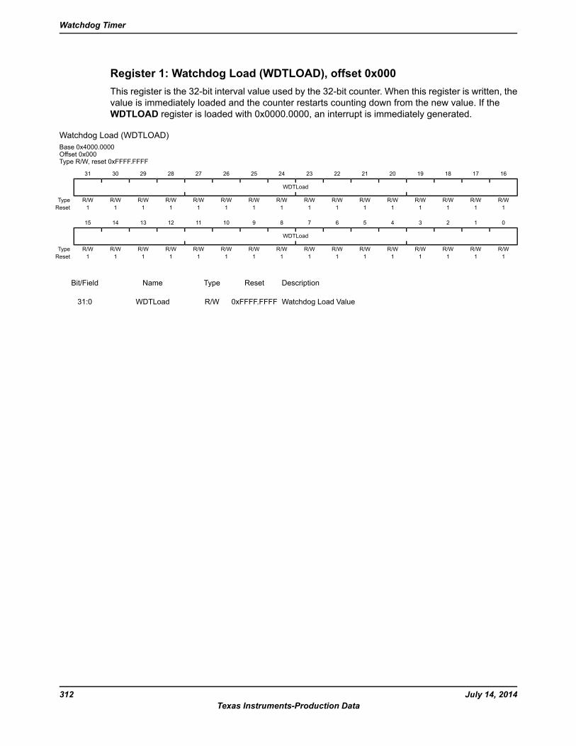
Register 1: Watchdog Load (WDTLOAD), offset 0x000This register is the 32-bit interval value used by the 32-bit counter. When this register is written, thevalue is immediately loaded and the counter restarts counting down from the new value. If theWDTLOAD register is loaded with 0x0000.0000, an interrupt is immediately generated.
Watchdog Load (WDTLOAD)Base 0x4000.0000Offset 0x000Type R/W, reset 0xFFFF.FFFF
16171819202122232425262728293031
WDTLoad
R/WR/WR/WR/WR/WR/WR/WR/WR/WR/WR/WR/WR/WR/WR/WR/WType1111111111111111Reset
0123456789101112131415
WDTLoad
R/WR/WR/WR/WR/WR/WR/WR/WR/WR/WR/WR/WR/WR/WR/WR/WType1111111111111111Reset
DescriptionResetTypeNameBit/Field
Watchdog Load Value0xFFFF.FFFFR/WWDTLoad31:0
July 14, 2014312Texas Instruments-Production Data
Watchdog Timer
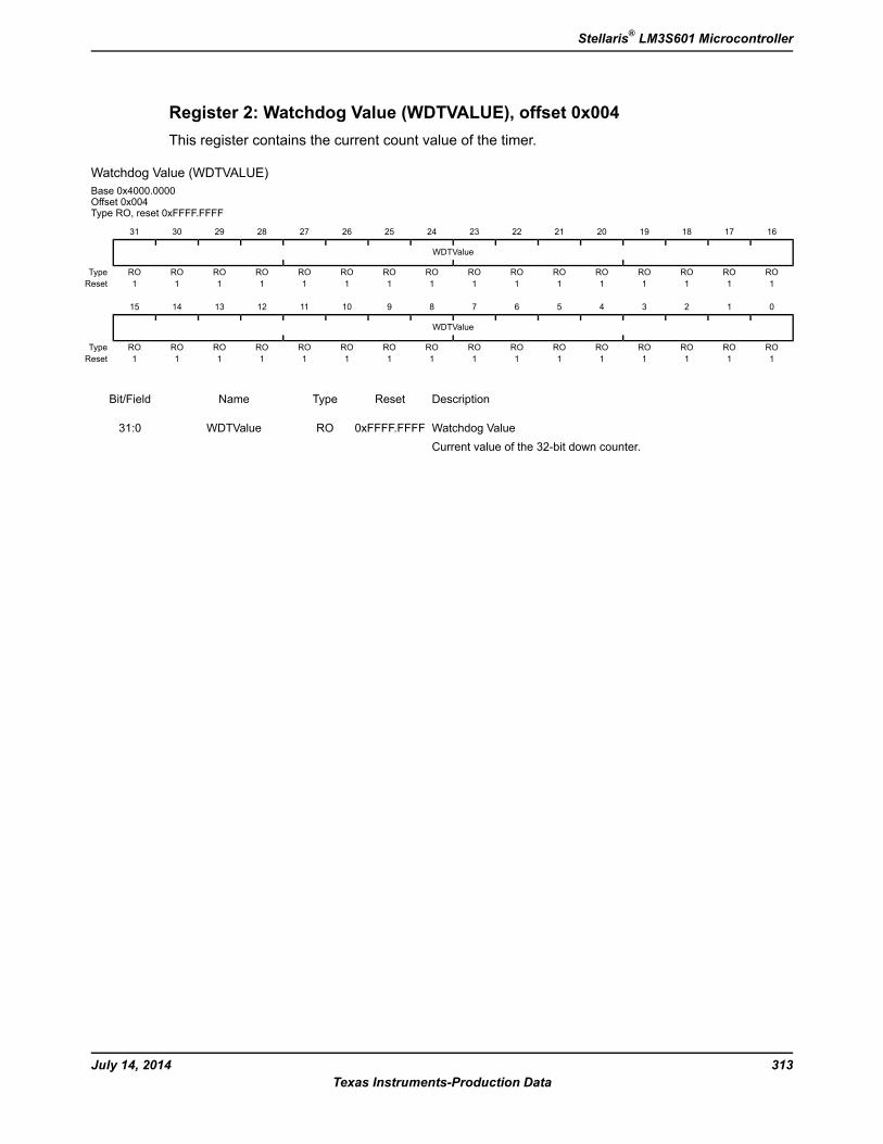
Register 2: Watchdog Value (WDTVALUE), offset 0x004This register contains the current count value of the timer.
Watchdog Value (WDTVALUE)Base 0x4000.0000Offset 0x004Type RO, reset 0xFFFF.FFFF
16171819202122232425262728293031
WDTValue
ROROROROROROROROROROROROROROROROType1111111111111111Reset
0123456789101112131415
WDTValue
ROROROROROROROROROROROROROROROROType1111111111111111Reset
DescriptionResetTypeNameBit/Field
Watchdog ValueCurrent value of the 32-bit down counter.
0xFFFF.FFFFROWDTValue31:0
313July 14, 2014Texas Instruments-Production Data
Stellaris® LM3S601 Microcontroller
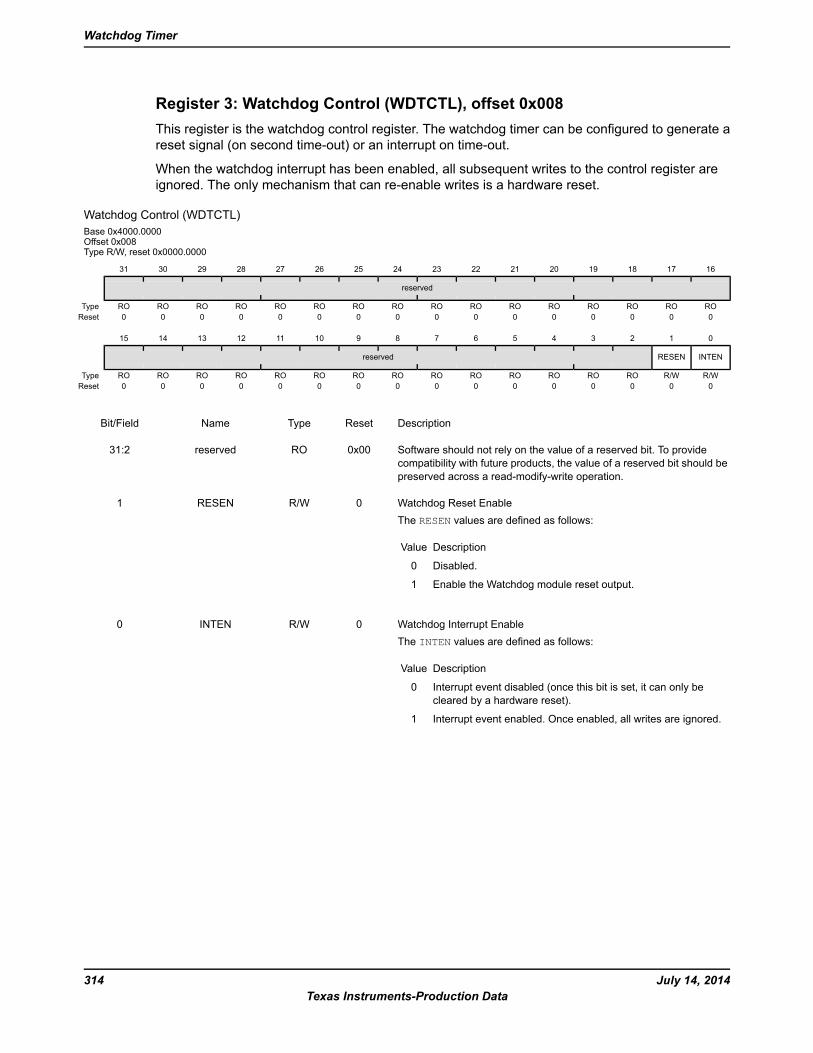
Register 3: Watchdog Control (WDTCTL), offset 0x008This register is the watchdog control register. The watchdog timer can be configured to generate areset signal (on second time-out) or an interrupt on time-out.
When the watchdog interrupt has been enabled, all subsequent writes to the control register areignored. The only mechanism that can re-enable writes is a hardware reset.
Watchdog Control (WDTCTL)Base 0x4000.0000Offset 0x008Type R/W, reset 0x0000.0000
16171819202122232425262728293031
reserved
ROROROROROROROROROROROROROROROROType0000000000000000Reset
0123456789101112131415
INTENRESENreserved
R/WR/WROROROROROROROROROROROROROROType0000000000000000Reset
DescriptionResetTypeNameBit/Field
Software should not rely on the value of a reserved bit. To providecompatibility with future products, the value of a reserved bit should bepreserved across a read-modify-write operation.
0x00ROreserved31:2
Watchdog Reset EnableThe RESEN values are defined as follows:
DescriptionValue
Disabled.0
Enable the Watchdog module reset output.1
0R/WRESEN1
Watchdog Interrupt EnableThe INTEN values are defined as follows:
DescriptionValue
Interrupt event disabled (once this bit is set, it can only becleared by a hardware reset).
0
Interrupt event enabled. Once enabled, all writes are ignored.1
0R/WINTEN0
July 14, 2014314Texas Instruments-Production Data
Watchdog Timer
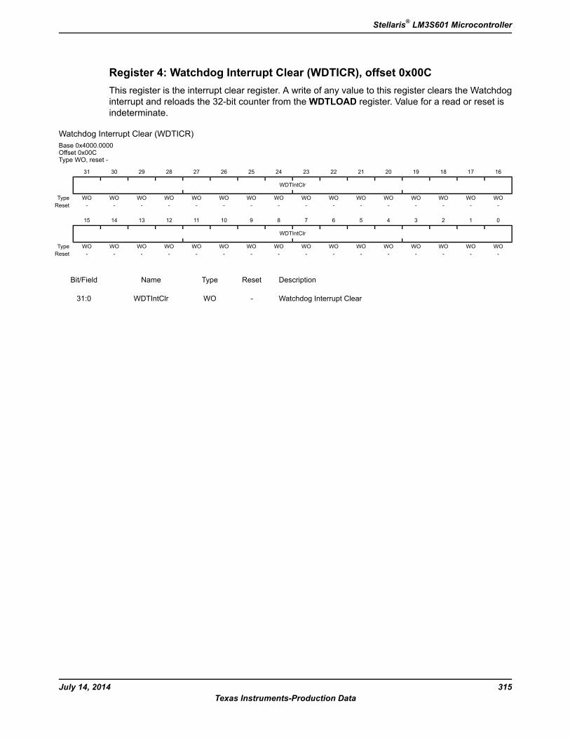
Register 4: Watchdog Interrupt Clear (WDTICR), offset 0x00CThis register is the interrupt clear register. A write of any value to this register clears the Watchdoginterrupt and reloads the 32-bit counter from theWDTLOAD register. Value for a read or reset isindeterminate.
Watchdog Interrupt Clear (WDTICR)Base 0x4000.0000Offset 0x00CType WO, reset -
16171819202122232425262728293031
WDTIntClr
WOWOWOWOWOWOWOWOWOWOWOWOWOWOWOWOType----------------Reset
0123456789101112131415
WDTIntClr
WOWOWOWOWOWOWOWOWOWOWOWOWOWOWOWOType----------------Reset
DescriptionResetTypeNameBit/Field
Watchdog Interrupt Clear-WOWDTIntClr31:0
315July 14, 2014Texas Instruments-Production Data
Stellaris® LM3S601 Microcontroller
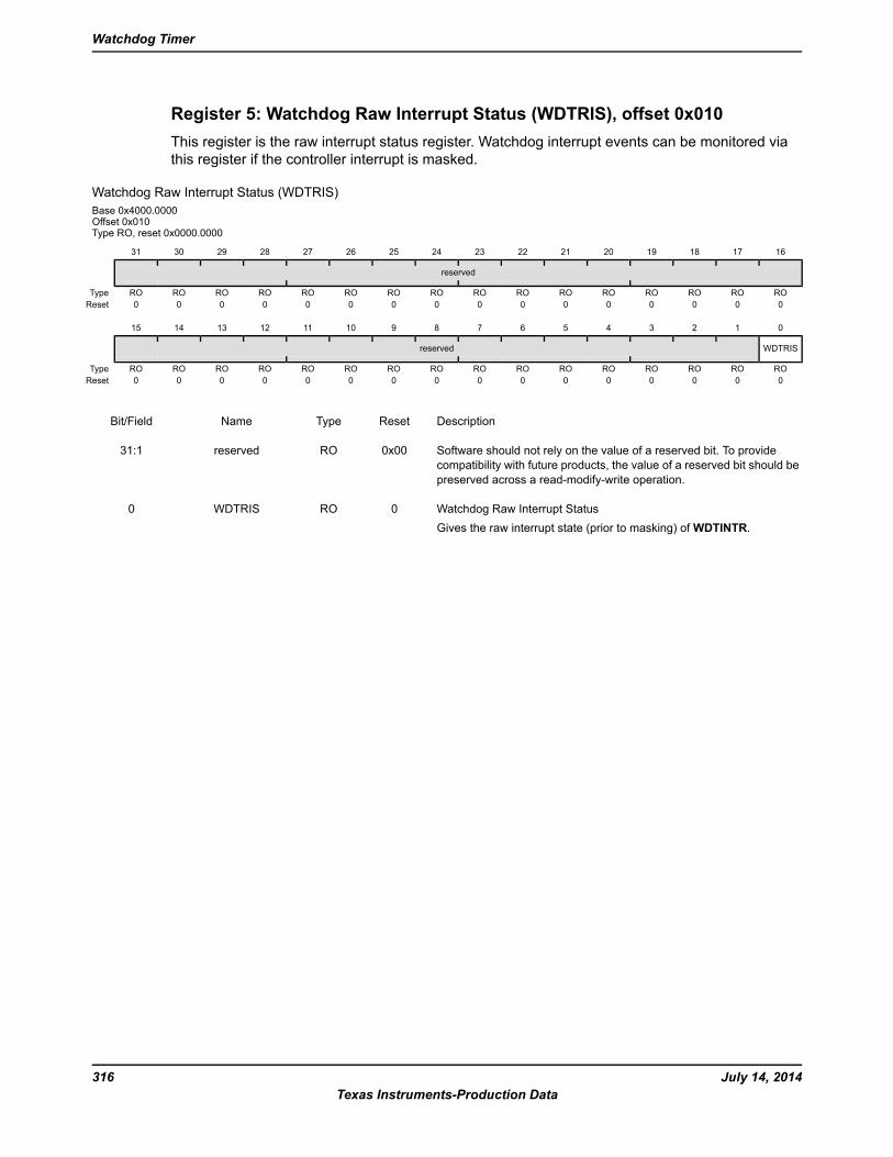
Register 5: Watchdog Raw Interrupt Status (WDTRIS), offset 0x010This register is the raw interrupt status register. Watchdog interrupt events can be monitored viathis register if the controller interrupt is masked.
Watchdog Raw Interrupt Status (WDTRIS)Base 0x4000.0000Offset 0x010Type RO, reset 0x0000.0000
16171819202122232425262728293031
reserved
ROROROROROROROROROROROROROROROROType0000000000000000Reset
0123456789101112131415
WDTRISreserved
ROROROROROROROROROROROROROROROROType0000000000000000Reset
DescriptionResetTypeNameBit/Field
Software should not rely on the value of a reserved bit. To providecompatibility with future products, the value of a reserved bit should bepreserved across a read-modify-write operation.
0x00ROreserved31:1
Watchdog Raw Interrupt StatusGives the raw interrupt state (prior to masking) ofWDTINTR.
0ROWDTRIS0
July 14, 2014316Texas Instruments-Production Data
Watchdog Timer
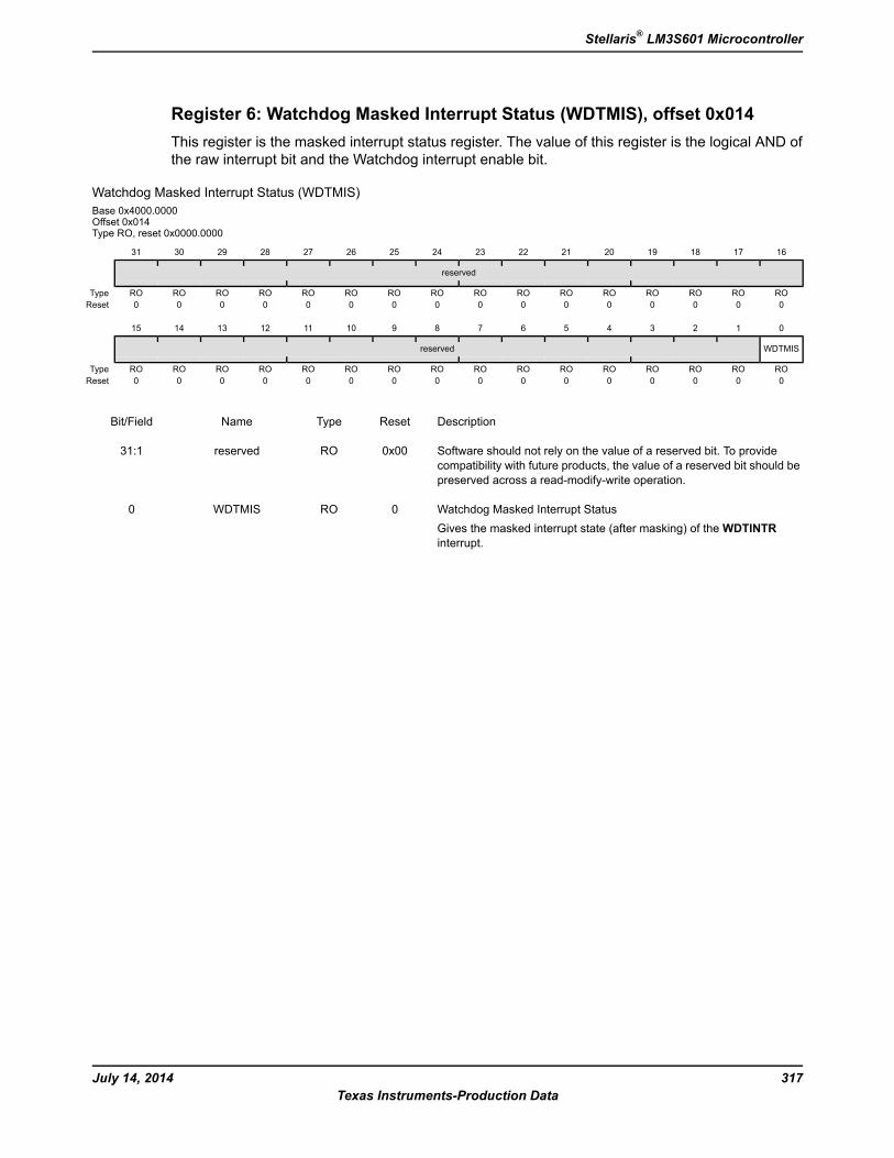
Register 6: Watchdog Masked Interrupt Status (WDTMIS), offset 0x014This register is the masked interrupt status register. The value of this register is the logical AND ofthe raw interrupt bit and the Watchdog interrupt enable bit.
Watchdog Masked Interrupt Status (WDTMIS)Base 0x4000.0000Offset 0x014Type RO, reset 0x0000.0000
16171819202122232425262728293031
reserved
ROROROROROROROROROROROROROROROROType0000000000000000Reset
0123456789101112131415
WDTMISreserved
ROROROROROROROROROROROROROROROROType0000000000000000Reset
DescriptionResetTypeNameBit/Field
Software should not rely on the value of a reserved bit. To providecompatibility with future products, the value of a reserved bit should bepreserved across a read-modify-write operation.
0x00ROreserved31:1
Watchdog Masked Interrupt StatusGives the masked interrupt state (after masking) of theWDTINTRinterrupt.
0ROWDTMIS0
317July 14, 2014Texas Instruments-Production Data
Stellaris® LM3S601 Microcontroller
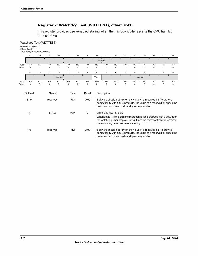
Register 7: Watchdog Test (WDTTEST), offset 0x418This register provides user-enabled stalling when the microcontroller asserts the CPU halt flagduring debug.
Watchdog Test (WDTTEST)Base 0x4000.0000Offset 0x418Type R/W, reset 0x0000.0000
16171819202122232425262728293031
reserved
ROROROROROROROROROROROROROROROROType0000000000000000Reset
0123456789101112131415
reservedSTALLreserved
ROROROROROROROROR/WROROROROROROROType0000000000000000Reset
DescriptionResetTypeNameBit/Field
Software should not rely on the value of a reserved bit. To providecompatibility with future products, the value of a reserved bit should bepreserved across a read-modify-write operation.
0x00ROreserved31:9
Watchdog Stall EnableWhen set to 1, if the Stellaris microcontroller is stopped with a debugger,the watchdog timer stops counting. Once the microcontroller is restarted,the watchdog timer resumes counting.
0R/WSTALL8
Software should not rely on the value of a reserved bit. To providecompatibility with future products, the value of a reserved bit should bepreserved across a read-modify-write operation.
0x00ROreserved7:0
July 14, 2014318Texas Instruments-Production Data
Watchdog Timer
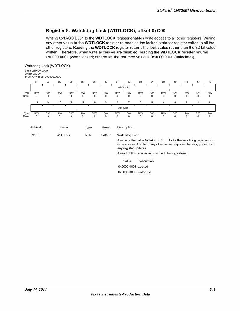
Register 8: Watchdog Lock (WDTLOCK), offset 0xC00Writing 0x1ACC.E551 to theWDTLOCK register enables write access to all other registers. Writingany other value to theWDTLOCK register re-enables the locked state for register writes to all theother registers. Reading theWDTLOCK register returns the lock status rather than the 32-bit valuewritten. Therefore, when write accesses are disabled, reading theWDTLOCK register returns0x0000.0001 (when locked; otherwise, the returned value is 0x0000.0000 (unlocked)).
Watchdog Lock (WDTLOCK)Base 0x4000.0000Offset 0xC00Type R/W, reset 0x0000.0000
16171819202122232425262728293031
WDTLock
R/WR/WR/WR/WR/WR/WR/WR/WR/WR/WR/WR/WR/WR/WR/WR/WType0000000000000000Reset
0123456789101112131415
WDTLock
R/WR/WR/WR/WR/WR/WR/WR/WR/WR/WR/WR/WR/WR/WR/WR/WType0000000000000000Reset
DescriptionResetTypeNameBit/Field
Watchdog LockA write of the value 0x1ACC.E551 unlocks the watchdog registers forwrite access. A write of any other value reapplies the lock, preventingany register updates.A read of this register returns the following values:
DescriptionValue
Locked0x0000.0001
Unlocked0x0000.0000
0x0000R/WWDTLock31:0
319July 14, 2014Texas Instruments-Production Data
Stellaris® LM3S601 Microcontroller

Register 9:Watchdog Peripheral Identification 4 (WDTPeriphID4), offset 0xFD0TheWDTPeriphIDn registers are hard-coded and the fields within the register determine the resetvalue.
Watchdog Peripheral Identification 4 (WDTPeriphID4)Base 0x4000.0000Offset 0xFD0Type RO, reset 0x0000.0000
16171819202122232425262728293031
reserved
ROROROROROROROROROROROROROROROROType0000000000000000Reset
0123456789101112131415
PID4reserved
ROROROROROROROROROROROROROROROROType0000000000000000Reset
DescriptionResetTypeNameBit/Field
Software should not rely on the value of a reserved bit. To providecompatibility with future products, the value of a reserved bit should bepreserved across a read-modify-write operation.
0x00ROreserved31:8
WDT Peripheral ID Register[7:0]0x00ROPID47:0
July 14, 2014320Texas Instruments-Production Data
Watchdog Timer
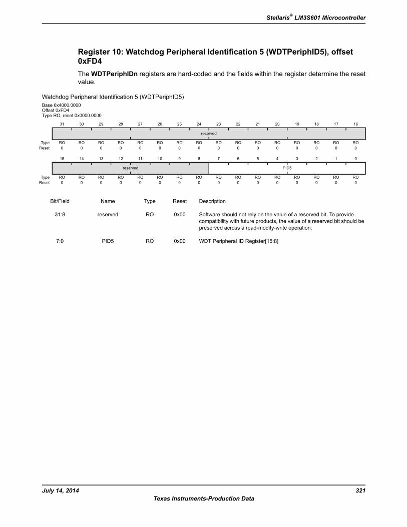
Register 10: Watchdog Peripheral Identification 5 (WDTPeriphID5), offset0xFD4TheWDTPeriphIDn registers are hard-coded and the fields within the register determine the resetvalue.
Watchdog Peripheral Identification 5 (WDTPeriphID5)Base 0x4000.0000Offset 0xFD4Type RO, reset 0x0000.0000
16171819202122232425262728293031
reserved
ROROROROROROROROROROROROROROROROType0000000000000000Reset
0123456789101112131415
PID5reserved
ROROROROROROROROROROROROROROROROType0000000000000000Reset
DescriptionResetTypeNameBit/Field
Software should not rely on the value of a reserved bit. To providecompatibility with future products, the value of a reserved bit should bepreserved across a read-modify-write operation.
0x00ROreserved31:8
WDT Peripheral ID Register[15:8]0x00ROPID57:0
321July 14, 2014Texas Instruments-Production Data
Stellaris® LM3S601 Microcontroller

Register 11: Watchdog Peripheral Identification 6 (WDTPeriphID6), offset0xFD8TheWDTPeriphIDn registers are hard-coded and the fields within the register determine the resetvalue.
Watchdog Peripheral Identification 6 (WDTPeriphID6)Base 0x4000.0000Offset 0xFD8Type RO, reset 0x0000.0000
16171819202122232425262728293031
reserved
ROROROROROROROROROROROROROROROROType0000000000000000Reset
0123456789101112131415
PID6reserved
ROROROROROROROROROROROROROROROROType0000000000000000Reset
DescriptionResetTypeNameBit/Field
Software should not rely on the value of a reserved bit. To providecompatibility with future products, the value of a reserved bit should bepreserved across a read-modify-write operation.
0x00ROreserved31:8
WDT Peripheral ID Register[23:16]0x00ROPID67:0
July 14, 2014322Texas Instruments-Production Data
Watchdog Timer

Register 12: Watchdog Peripheral Identification 7 (WDTPeriphID7), offset0xFDCTheWDTPeriphIDn registers are hard-coded and the fields within the register determine the resetvalue.
Watchdog Peripheral Identification 7 (WDTPeriphID7)Base 0x4000.0000Offset 0xFDCType RO, reset 0x0000.0000
16171819202122232425262728293031
reserved
ROROROROROROROROROROROROROROROROType0000000000000000Reset
0123456789101112131415
PID7reserved
ROROROROROROROROROROROROROROROROType0000000000000000Reset
DescriptionResetTypeNameBit/Field
Software should not rely on the value of a reserved bit. To providecompatibility with future products, the value of a reserved bit should bepreserved across a read-modify-write operation.
0x00ROreserved31:8
WDT Peripheral ID Register[31:24]0x00ROPID77:0
323July 14, 2014Texas Instruments-Production Data
Stellaris® LM3S601 Microcontroller
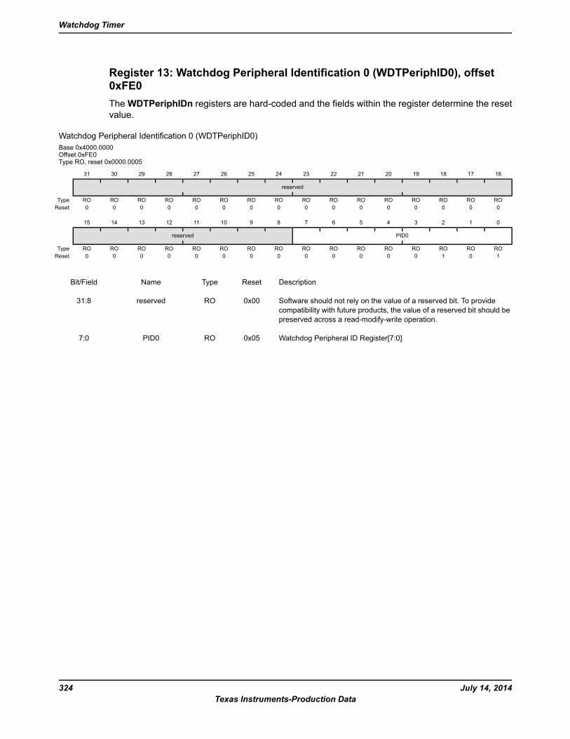
Register 13: Watchdog Peripheral Identification 0 (WDTPeriphID0), offset0xFE0TheWDTPeriphIDn registers are hard-coded and the fields within the register determine the resetvalue.
Watchdog Peripheral Identification 0 (WDTPeriphID0)Base 0x4000.0000Offset 0xFE0Type RO, reset 0x0000.0005
16171819202122232425262728293031
reserved
ROROROROROROROROROROROROROROROROType0000000000000000Reset
0123456789101112131415
PID0reserved
ROROROROROROROROROROROROROROROROType1010000000000000Reset
DescriptionResetTypeNameBit/Field
Software should not rely on the value of a reserved bit. To providecompatibility with future products, the value of a reserved bit should bepreserved across a read-modify-write operation.
0x00ROreserved31:8
Watchdog Peripheral ID Register[7:0]0x05ROPID07:0
July 14, 2014324Texas Instruments-Production Data
Watchdog Timer

Register 14: Watchdog Peripheral Identification 1 (WDTPeriphID1), offset0xFE4TheWDTPeriphIDn registers are hard-coded and the fields within the register determine the resetvalue.
Watchdog Peripheral Identification 1 (WDTPeriphID1)Base 0x4000.0000Offset 0xFE4Type RO, reset 0x0000.0018
16171819202122232425262728293031
reserved
ROROROROROROROROROROROROROROROROType0000000000000000Reset
0123456789101112131415
PID1reserved
ROROROROROROROROROROROROROROROROType0001100000000000Reset
DescriptionResetTypeNameBit/Field
Software should not rely on the value of a reserved bit. To providecompatibility with future products, the value of a reserved bit should bepreserved across a read-modify-write operation.
0x00ROreserved31:8
Watchdog Peripheral ID Register[15:8]0x18ROPID17:0
325July 14, 2014Texas Instruments-Production Data
Stellaris® LM3S601 Microcontroller

Register 15: Watchdog Peripheral Identification 2 (WDTPeriphID2), offset0xFE8TheWDTPeriphIDn registers are hard-coded and the fields within the register determine the resetvalue.
Watchdog Peripheral Identification 2 (WDTPeriphID2)Base 0x4000.0000Offset 0xFE8Type RO, reset 0x0000.0018
16171819202122232425262728293031
reserved
ROROROROROROROROROROROROROROROROType0000000000000000Reset
0123456789101112131415
PID2reserved
ROROROROROROROROROROROROROROROROType0001100000000000Reset
DescriptionResetTypeNameBit/Field
Software should not rely on the value of a reserved bit. To providecompatibility with future products, the value of a reserved bit should bepreserved across a read-modify-write operation.
0x00ROreserved31:8
Watchdog Peripheral ID Register[23:16]0x18ROPID27:0
July 14, 2014326Texas Instruments-Production Data
Watchdog Timer
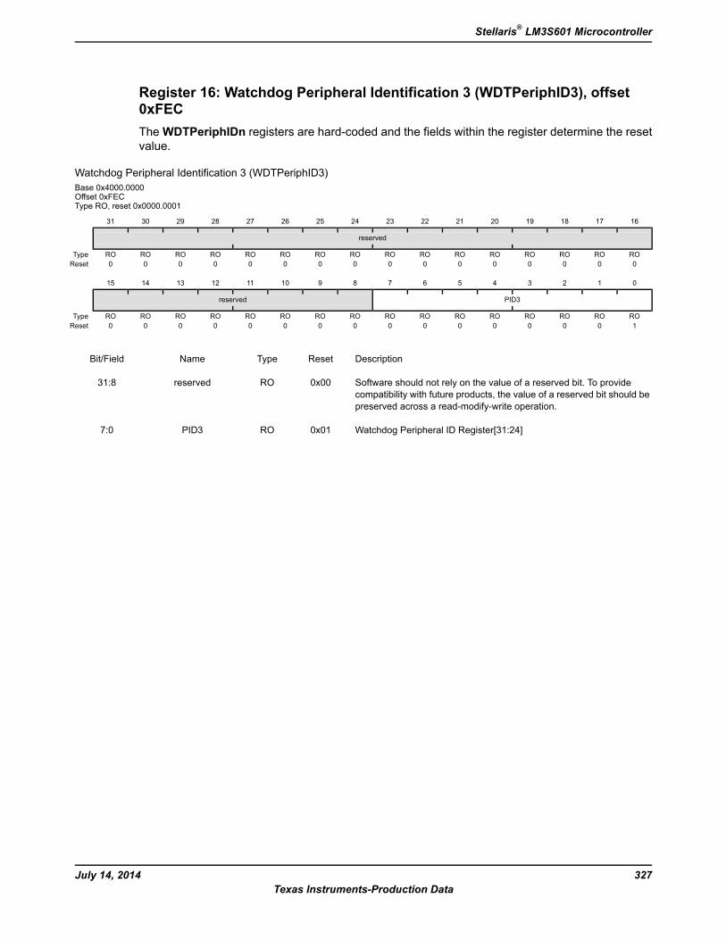
Register 16: Watchdog Peripheral Identification 3 (WDTPeriphID3), offset0xFECTheWDTPeriphIDn registers are hard-coded and the fields within the register determine the resetvalue.
Watchdog Peripheral Identification 3 (WDTPeriphID3)Base 0x4000.0000Offset 0xFECType RO, reset 0x0000.0001
16171819202122232425262728293031
reserved
ROROROROROROROROROROROROROROROROType0000000000000000Reset
0123456789101112131415
PID3reserved
ROROROROROROROROROROROROROROROROType1000000000000000Reset
DescriptionResetTypeNameBit/Field
Software should not rely on the value of a reserved bit. To providecompatibility with future products, the value of a reserved bit should bepreserved across a read-modify-write operation.
0x00ROreserved31:8
Watchdog Peripheral ID Register[31:24]0x01ROPID37:0
327July 14, 2014Texas Instruments-Production Data
Stellaris® LM3S601 Microcontroller

Register 17: Watchdog PrimeCell Identification 0 (WDTPCellID0), offset 0xFF0TheWDTPCellIDn registers are hard-coded and the fields within the register determine the resetvalue.
Watchdog PrimeCell Identification 0 (WDTPCellID0)Base 0x4000.0000Offset 0xFF0Type RO, reset 0x0000.000D
16171819202122232425262728293031
reserved
ROROROROROROROROROROROROROROROROType0000000000000000Reset
0123456789101112131415
CID0reserved
ROROROROROROROROROROROROROROROROType1011000000000000Reset
DescriptionResetTypeNameBit/Field
Software should not rely on the value of a reserved bit. To providecompatibility with future products, the value of a reserved bit should bepreserved across a read-modify-write operation.
0x00ROreserved31:8
Watchdog PrimeCell ID Register[7:0]0x0DROCID07:0
July 14, 2014328Texas Instruments-Production Data
Watchdog Timer
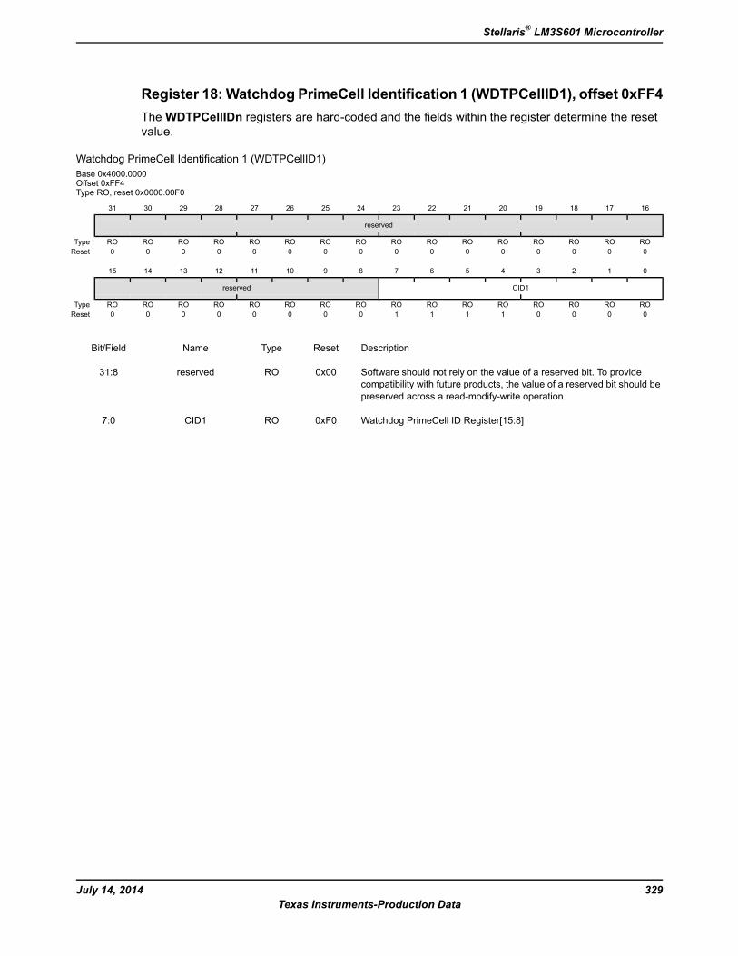
Register 18: Watchdog PrimeCell Identification 1 (WDTPCellID1), offset 0xFF4TheWDTPCellIDn registers are hard-coded and the fields within the register determine the resetvalue.
Watchdog PrimeCell Identification 1 (WDTPCellID1)Base 0x4000.0000Offset 0xFF4Type RO, reset 0x0000.00F0
16171819202122232425262728293031
reserved
ROROROROROROROROROROROROROROROROType0000000000000000Reset
0123456789101112131415
CID1reserved
ROROROROROROROROROROROROROROROROType0000111100000000Reset
DescriptionResetTypeNameBit/Field
Software should not rely on the value of a reserved bit. To providecompatibility with future products, the value of a reserved bit should bepreserved across a read-modify-write operation.
0x00ROreserved31:8
Watchdog PrimeCell ID Register[15:8]0xF0ROCID17:0
329July 14, 2014Texas Instruments-Production Data
Stellaris® LM3S601 Microcontroller
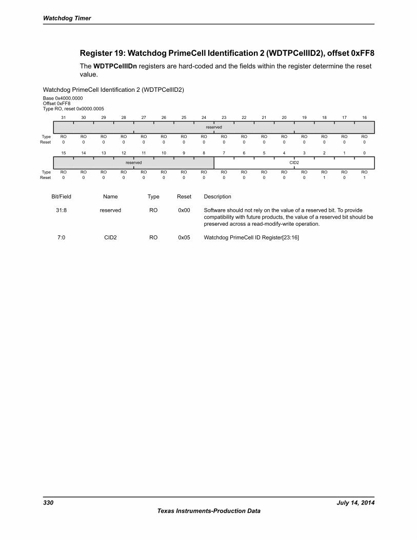
Register 19: Watchdog PrimeCell Identification 2 (WDTPCellID2), offset 0xFF8TheWDTPCellIDn registers are hard-coded and the fields within the register determine the resetvalue.
Watchdog PrimeCell Identification 2 (WDTPCellID2)Base 0x4000.0000Offset 0xFF8Type RO, reset 0x0000.0005
16171819202122232425262728293031
reserved
ROROROROROROROROROROROROROROROROType0000000000000000Reset
0123456789101112131415
CID2reserved
ROROROROROROROROROROROROROROROROType1010000000000000Reset
DescriptionResetTypeNameBit/Field
Software should not rely on the value of a reserved bit. To providecompatibility with future products, the value of a reserved bit should bepreserved across a read-modify-write operation.
0x00ROreserved31:8
Watchdog PrimeCell ID Register[23:16]0x05ROCID27:0
July 14, 2014330Texas Instruments-Production Data
Watchdog Timer
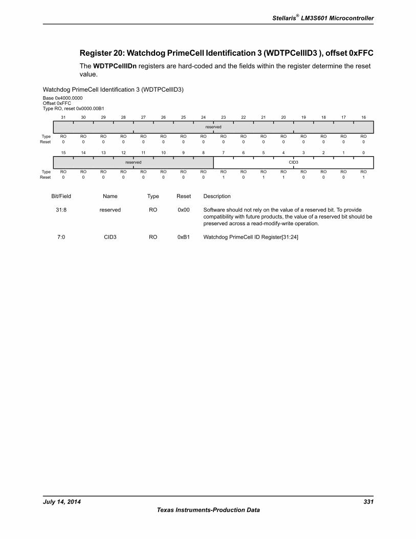
Register 20:Watchdog PrimeCell Identification 3 (WDTPCellID3 ), offset 0xFFCTheWDTPCellIDn registers are hard-coded and the fields within the register determine the resetvalue.
Watchdog PrimeCell Identification 3 (WDTPCellID3)Base 0x4000.0000Offset 0xFFCType RO, reset 0x0000.00B1
16171819202122232425262728293031
reserved
ROROROROROROROROROROROROROROROROType0000000000000000Reset
0123456789101112131415
CID3reserved
ROROROROROROROROROROROROROROROROType1000110100000000Reset
DescriptionResetTypeNameBit/Field
Software should not rely on the value of a reserved bit. To providecompatibility with future products, the value of a reserved bit should bepreserved across a read-modify-write operation.
0x00ROreserved31:8
Watchdog PrimeCell ID Register[31:24]0xB1ROCID37:0
331July 14, 2014Texas Instruments-Production Data
Stellaris® LM3S601 Microcontroller
10 Universal Asynchronous Receivers/Transmitters(UARTs)Each Stellaris® Universal Asynchronous Receiver/Transmitter (UART) has the following features:
Two fully programmable 16C550-type UARTs
Separate 16x8 transmit (TX) and receive (RX) FIFOs to reduce CPU interrupt service loading
Programmable baud-rate generator allowing speeds up to 3.125 Mbps
Programmable FIFO length, including 1-byte deep operation providing conventionaldouble-buffered interface
FIFO trigger levels of 1/8, 1/4, 1/2, 3/4, and 7/8
Standard asynchronous communication bits for start, stop, and parity
Line-break generation and detection
Fully programmable serial interface characteristics
– 5, 6, 7, or 8 data bits
– Even, odd, stick, or no-parity bit generation/detection
– 1 or 2 stop bit generation
July 14, 2014332Texas Instruments-Production Data
Universal Asynchronous Receivers/Transmitters (UARTs)
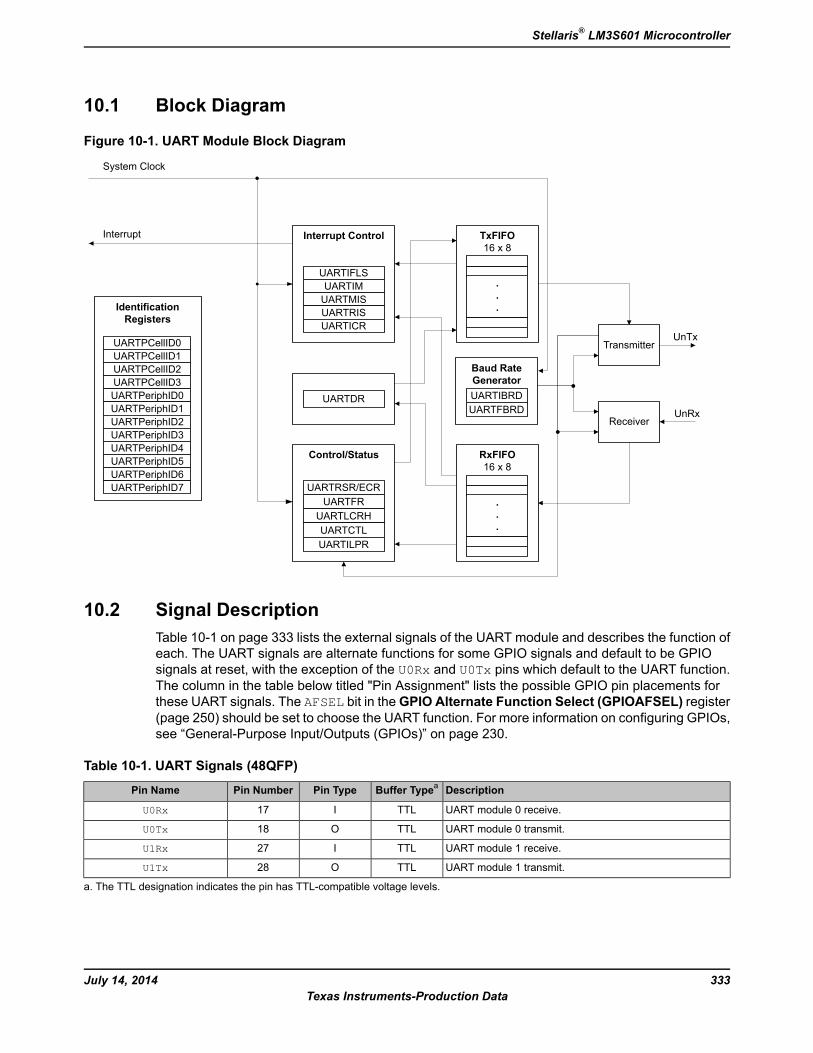
10.1 Block Diagram
Figure 10-1. UART Module Block Diagram
TxFIFO16 x 8
.
.
.
RxFIFO16 x 8
.
.
.
IdentificationRegisters
UARTPCellID0UARTPCellID1UARTPCellID2UARTPCellID3UARTPeriphID0UARTPeriphID1UARTPeriphID2UARTPeriphID3UARTPeriphID4UARTPeriphID5UARTPeriphID6UARTPeriphID7
Interrupt Control
UARTDR
Control/Status
Transmitter
Baud RateGenerator
Receiver
UnTx
UnRx
System Clock
Interrupt
UARTRSR/ECRUARTFR
UARTLCRHUARTCTLUARTILPR
UARTIFLSUARTIMUARTMISUARTRISUARTICR
UARTIBRDUARTFBRD
10.2 Signal DescriptionTable 10-1 on page 333 lists the external signals of the UART module and describes the function ofeach. The UART signals are alternate functions for some GPIO signals and default to be GPIOsignals at reset, with the exception of the U0Rx and U0Tx pins which default to the UART function.The column in the table below titled "Pin Assignment" lists the possible GPIO pin placements forthese UART signals. The AFSEL bit in theGPIO Alternate Function Select (GPIOAFSEL) register(page 250) should be set to choose the UART function. For more information on configuring GPIOs,see “General-Purpose Input/Outputs (GPIOs)” on page 230.
Table 10-1. UART Signals (48QFP)
DescriptionBuffer TypeaPin TypePin NumberPin Name
UART module 0 receive.TTLI17U0Rx
UART module 0 transmit.TTLO18U0Tx
UART module 1 receive.TTLI27U1Rx
UART module 1 transmit.TTLO28U1Tx
a. The TTL designation indicates the pin has TTL-compatible voltage levels.
333July 14, 2014Texas Instruments-Production Data
Stellaris® LM3S601 Microcontroller
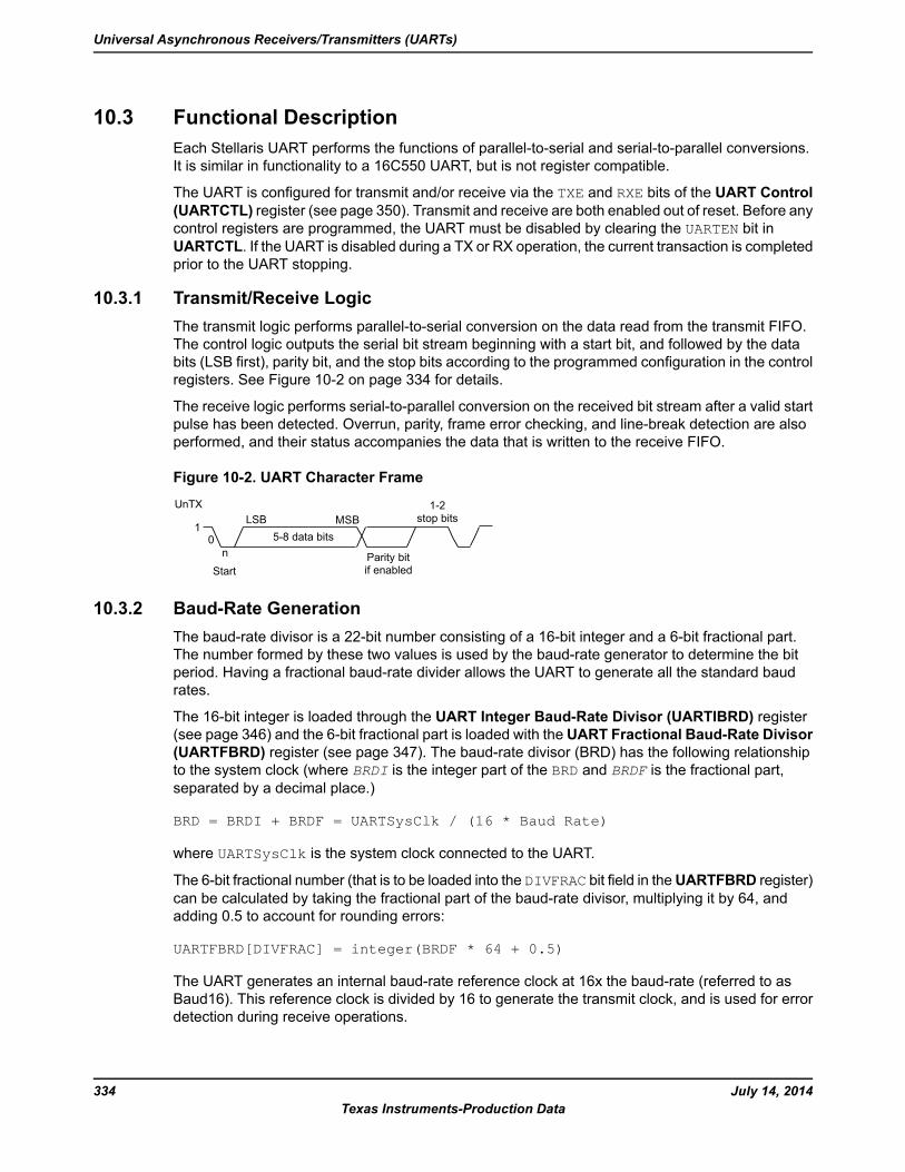
10.3 Functional DescriptionEach Stellaris UART performs the functions of parallel-to-serial and serial-to-parallel conversions.It is similar in functionality to a 16C550 UART, but is not register compatible.
The UART is configured for transmit and/or receive via the TXE and RXE bits of the UART Control(UARTCTL) register (see page 350). Transmit and receive are both enabled out of reset. Before anycontrol registers are programmed, the UART must be disabled by clearing the UARTEN bit inUARTCTL. If the UART is disabled during a TX or RX operation, the current transaction is completedprior to the UART stopping.
10.3.1 Transmit/Receive LogicThe transmit logic performs parallel-to-serial conversion on the data read from the transmit FIFO.The control logic outputs the serial bit stream beginning with a start bit, and followed by the databits (LSB first), parity bit, and the stop bits according to the programmed configuration in the controlregisters. See Figure 10-2 on page 334 for details.
The receive logic performs serial-to-parallel conversion on the received bit stream after a valid startpulse has been detected. Overrun, parity, frame error checking, and line-break detection are alsoperformed, and their status accompanies the data that is written to the receive FIFO.
Figure 10-2. UART Character Frame
10 5-8 data bits
LSB MSB
Parity bitif enabled
1-2stop bits
UnTX
n
Start
10.3.2 Baud-Rate GenerationThe baud-rate divisor is a 22-bit number consisting of a 16-bit integer and a 6-bit fractional part.The number formed by these two values is used by the baud-rate generator to determine the bitperiod. Having a fractional baud-rate divider allows the UART to generate all the standard baudrates.
The 16-bit integer is loaded through the UART Integer Baud-Rate Divisor (UARTIBRD) register(see page 346) and the 6-bit fractional part is loaded with the UART Fractional Baud-Rate Divisor(UARTFBRD) register (see page 347). The baud-rate divisor (BRD) has the following relationshipto the system clock (where BRDI is the integer part of the BRD and BRDF is the fractional part,separated by a decimal place.)
BRD = BRDI + BRDF = UARTSysClk / (16 * Baud Rate)
where UARTSysClk is the system clock connected to the UART.
The 6-bit fractional number (that is to be loaded into the DIVFRAC bit field in theUARTFBRD register)can be calculated by taking the fractional part of the baud-rate divisor, multiplying it by 64, andadding 0.5 to account for rounding errors:
UARTFBRD[DIVFRAC] = integer(BRDF * 64 + 0.5)
The UART generates an internal baud-rate reference clock at 16x the baud-rate (referred to asBaud16). This reference clock is divided by 16 to generate the transmit clock, and is used for errordetection during receive operations.
July 14, 2014334Texas Instruments-Production Data
Universal Asynchronous Receivers/Transmitters (UARTs)
Along with theUARTLineControl, HighByte (UARTLCRH) register (see page 348), theUARTIBRDand UARTFBRD registers form an internal 30-bit register. This internal register is only updatedwhen a write operation to UARTLCRH is performed, so any changes to the baud-rate divisor mustbe followed by a write to the UARTLCRH register for the changes to take effect.
To update the baud-rate registers, there are four possible sequences:
UARTIBRD write, UARTFBRD write, and UARTLCRH write
UARTFBRD write, UARTIBRD write, and UARTLCRH write
UARTIBRD write and UARTLCRH write
UARTFBRD write and UARTLCRH write
10.3.3 Data TransmissionData received or transmitted is stored in two 16-byte FIFOs, though the receive FIFO has an extrafour bits per character for status information. For transmission, data is written into the transmit FIFO.If the UART is enabled, it causes a data frame to start transmitting with the parameters indicatedin theUARTLCRH register. Data continues to be transmitted until there is no data left in the transmitFIFO. The BUSY bit in the UART Flag (UARTFR) register (see page 344) is asserted as soon asdata is written to the transmit FIFO (that is, if the FIFO is non-empty) and remains asserted whiledata is being transmitted. The BUSY bit is negated only when the transmit FIFO is empty, and thelast character has been transmitted from the shift register, including the stop bits. The UART canindicate that it is busy even though the UART may no longer be enabled.
When the receiver is idle (the UnRx is continuously 1) and the data input goes Low (a start bit hasbeen received), the receive counter begins running and data is sampled on the eighth cycle ofBaud16 (described in “Transmit/Receive Logic” on page 334).
The start bit is valid and recognized if UnRx is still low on the eighth cycle of Baud16, otherwise itis ignored. After a valid start bit is detected, successive data bits are sampled on every 16th cycleof Baud16 (that is, one bit period later) according to the programmed length of the data characters.The parity bit is then checked if parity mode was enabled. Data length and parity are defined in theUARTLCRH register.
Lastly, a valid stop bit is confirmed if UnRx is High, otherwise a framing error has occurred. Whena full word is received, the data is stored in the receive FIFO, with any error bits associated withthat word.
10.3.4 FIFO OperationThe UART has two 16-entry FIFOs; one for transmit and one for receive. Both FIFOs are accessedvia the UART Data (UARTDR) register (see page 340). Read operations of the UARTDR registerreturn a 12-bit value consisting of 8 data bits and 4 error flags while write operations place 8-bit datain the transmit FIFO.
Out of reset, both FIFOs are disabled and act as 1-byte-deep holding registers. The FIFOs areenabled by setting the FEN bit in UARTLCRH (page 348).
FIFO status can be monitored via theUART Flag (UARTFR) register (see page 344) and theUARTReceive Status (UARTRSR) register. Hardware monitors empty, full and overrun conditions. TheUARTFR register contains empty and full flags (TXFE, TXFF, RXFE, and RXFF bits) and theUARTRSR register shows overrun status via the OE bit.
335July 14, 2014Texas Instruments-Production Data
Stellaris® LM3S601 Microcontroller
The trigger points at which the FIFOs generate interrupts is controlled via the UART Interrupt FIFOLevel Select (UARTIFLS) register (see page 352). Both FIFOs can be individually configured totrigger interrupts at different levels. Available configurations include 1/8, ¼, ½, ¾, and 7/8. Forexample, if the ¼ option is selected for the receive FIFO, the UART generates a receive interruptafter 4 data bytes are received. Out of reset, both FIFOs are configured to trigger an interrupt at the½ mark.
10.3.5 InterruptsThe UART can generate interrupts when the following conditions are observed:
Overrun Error
Break Error
Parity Error
Framing Error
Receive Timeout
Transmit (when condition defined in the TXIFLSEL bit in the UARTIFLS register is met)
Receive (when condition defined in the RXIFLSEL bit in the UARTIFLS register is met)
All of the interrupt events are ORed together before being sent to the interrupt controller, so theUART can only generate a single interrupt request to the controller at any given time. Software canservice multiple interrupt events in a single interrupt service routine by reading the UART MaskedInterrupt Status (UARTMIS) register (see page 357).
The interrupt events that can trigger a controller-level interrupt are defined in the UART InterruptMask (UARTIM ) register (see page 354) by setting the corresponding IM bit to 1. If interrupts arenot used, the raw interrupt status is always visible via the UART Raw Interrupt Status (UARTRIS)register (see page 356).
Interrupts are always cleared (for both the UARTMIS and UARTRIS registers) by setting thecorresponding bit in the UART Interrupt Clear (UARTICR) register (see page 358).
The receive interrupt changes state when one of the following events occurs:
If the FIFOs are enabled and the receive FIFO reaches the programmed trigger level, the RXRISbit is set. The receive interrupt is cleared by reading data from the receive FIFO until it becomesless than the trigger level, or by clearing the interrupt by writing a 1 to the RXIC bit.
If the FIFOs are disabled (have a depth of one location) and data is received thereby filling thelocation, the RXRIS bit is set. The receive interrupt is cleared by performing a single read of thereceive FIFO, or by clearing the interrupt by writing a 1 to the RXIC bit.
The transmit interrupt changes state when one of the following events occurs:
If the FIFOs are enabled and the transmit FIFO progresses through the programmed triggerlevel, the TXRIS bit is set. The transmit interrupt is based on a transition through level, thereforethe FIFOmust be written past the programmed trigger level otherwise no further transmit interruptswill be generated. The transmit interrupt is cleared by writing data to the transmit FIFO until itbecomes greater than the trigger level, or by clearing the interrupt by writing a 1 to the TXIC bit.
July 14, 2014336Texas Instruments-Production Data
Universal Asynchronous Receivers/Transmitters (UARTs)
If the FIFOs are disabled (have a depth of one location) and there is no data present in thetransmitters single location, the TXRIS bit is set. It is cleared by performing a single write to thetransmit FIFO, or by clearing the interrupt by writing a 1 to the TXIC bit.
10.3.6 Loopback OperationThe UART can be placed into an internal loopback mode for diagnostic or debug work. This isaccomplished by setting the LBE bit in the UARTCTL register (see page 350). In loopback mode,data transmitted on UnTx is received on the UnRx input.
10.4 Initialization and ConfigurationTo use the UARTs, the peripheral clock must be enabled by setting the UART0 or UART1 bits in theRCGC1 register.
This section discusses the steps that are required to use a UART module. For this example, theUART clock is assumed to be 20 MHz and the desired UART configuration is:
115200 baud rate
Data length of 8 bits
One stop bit
No parity
FIFOs disabled
No interrupts
The first thing to consider when programming the UART is the baud-rate divisor (BRD), since theUARTIBRD and UARTFBRD registers must be written before the UARTLCRH register. Using theequation described in “Baud-Rate Generation” on page 334, the BRD can be calculated:
BRD = 20,000,000 / (16 * 115,200) = 10.8507
which means that the DIVINT field of the UARTIBRD register (see page 346) should be set to 10.The value to be loaded into the UARTFBRD register (see page 347) is calculated by the equation:
UARTFBRD[DIVFRAC] = integer(0.8507 * 64 + 0.5) = 54
With the BRD values in hand, the UART configuration is written to the module in the following order:
1. Disable the UART by clearing the UARTEN bit in the UARTCTL register.
2. Write the integer portion of the BRD to the UARTIBRD register.
3. Write the fractional portion of the BRD to the UARTFBRD register.
4. Write the desired serial parameters to the UARTLCRH register (in this case, a value of0x0000.0060).
5. Enable the UART by setting the UARTEN bit in the UARTCTL register.
337July 14, 2014Texas Instruments-Production Data
Stellaris® LM3S601 Microcontroller
10.5 Register MapTable 10-2 on page 338 lists the UART registers. The offset listed is a hexadecimal increment to theregister’s address, relative to that UART’s base address:
UART0: 0x4000.C000 UART1: 0x4000.D000
Note that the UART module clock must be enabled before the registers can be programmed (seepage 194). There must be a delay of 3 system clocks after the UARTmodule clock is enabled beforeany UART module registers are accessed.
Note: The UART must be disabled (see the UARTEN bit in the UARTCTL register on page 350)before any of the control registers are reprogrammed. When the UART is disabled duringa TX or RX operation, the current transaction is completed prior to the UART stopping.
Table 10-2. UART Register Map
SeepageDescriptionResetTypeNameOffset
340UART Data0x0000.0000R/WUARTDR0x000
342UART Receive Status/Error Clear0x0000.0000R/WUARTRSR/UARTECR0x004
344UART Flag0x0000.0090ROUARTFR0x018
346UART Integer Baud-Rate Divisor0x0000.0000R/WUARTIBRD0x024
347UART Fractional Baud-Rate Divisor0x0000.0000R/WUARTFBRD0x028
348UART Line Control0x0000.0000R/WUARTLCRH0x02C
350UART Control0x0000.0300R/WUARTCTL0x030
352UART Interrupt FIFO Level Select0x0000.0012R/WUARTIFLS0x034
354UART Interrupt Mask0x0000.0000R/WUARTIM0x038
356UART Raw Interrupt Status0x0000.0000ROUARTRIS0x03C
357UART Masked Interrupt Status0x0000.0000ROUARTMIS0x040
358UART Interrupt Clear0x0000.0000W1CUARTICR0x044
360UART Peripheral Identification 40x0000.0000ROUARTPeriphID40xFD0
361UART Peripheral Identification 50x0000.0000ROUARTPeriphID50xFD4
362UART Peripheral Identification 60x0000.0000ROUARTPeriphID60xFD8
363UART Peripheral Identification 70x0000.0000ROUARTPeriphID70xFDC
364UART Peripheral Identification 00x0000.0011ROUARTPeriphID00xFE0
365UART Peripheral Identification 10x0000.0000ROUARTPeriphID10xFE4
366UART Peripheral Identification 20x0000.0018ROUARTPeriphID20xFE8
367UART Peripheral Identification 30x0000.0001ROUARTPeriphID30xFEC
368UART PrimeCell Identification 00x0000.000DROUARTPCellID00xFF0
369UART PrimeCell Identification 10x0000.00F0ROUARTPCellID10xFF4
July 14, 2014338Texas Instruments-Production Data
Universal Asynchronous Receivers/Transmitters (UARTs)
Table 10-2. UART Register Map (continued)
SeepageDescriptionResetTypeNameOffset
370UART PrimeCell Identification 20x0000.0005ROUARTPCellID20xFF8
371UART PrimeCell Identification 30x0000.00B1ROUARTPCellID30xFFC
10.6 Register DescriptionsThe remainder of this section lists and describes the UART registers, in numerical order by addressoffset.
339July 14, 2014Texas Instruments-Production Data
Stellaris® LM3S601 Microcontroller
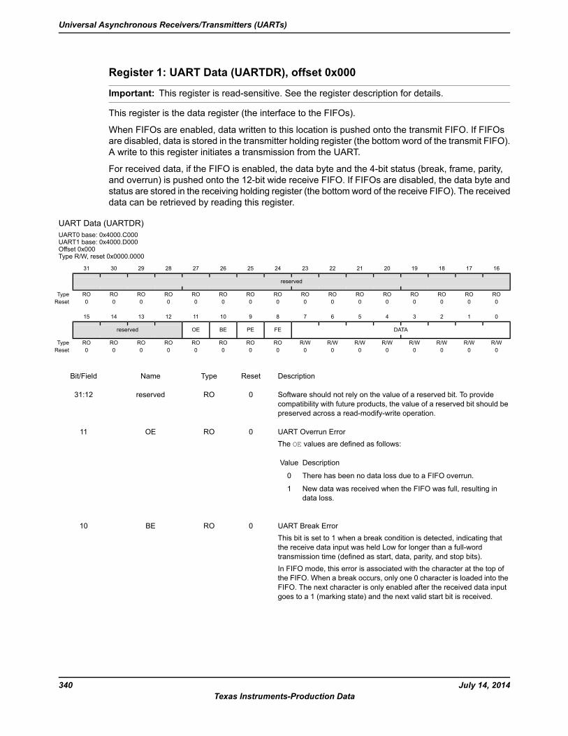
Register 1: UART Data (UARTDR), offset 0x000
Important: This register is read-sensitive. See the register description for details.
This register is the data register (the interface to the FIFOs).
When FIFOs are enabled, data written to this location is pushed onto the transmit FIFO. If FIFOsare disabled, data is stored in the transmitter holding register (the bottom word of the transmit FIFO).A write to this register initiates a transmission from the UART.
For received data, if the FIFO is enabled, the data byte and the 4-bit status (break, frame, parity,and overrun) is pushed onto the 12-bit wide receive FIFO. If FIFOs are disabled, the data byte andstatus are stored in the receiving holding register (the bottom word of the receive FIFO). The receiveddata can be retrieved by reading this register.
UART Data (UARTDR)UART0 base: 0x4000.C000UART1 base: 0x4000.D000Offset 0x000Type R/W, reset 0x0000.0000
16171819202122232425262728293031
reserved
ROROROROROROROROROROROROROROROROType0000000000000000Reset
0123456789101112131415
DATAFEPEBEOEreserved
R/WR/WR/WR/WR/WR/WR/WR/WROROROROROROROROType0000000000000000Reset
DescriptionResetTypeNameBit/Field
Software should not rely on the value of a reserved bit. To providecompatibility with future products, the value of a reserved bit should bepreserved across a read-modify-write operation.
0ROreserved31:12
UART Overrun ErrorThe OE values are defined as follows:
DescriptionValue
There has been no data loss due to a FIFO overrun.0
New data was received when the FIFO was full, resulting indata loss.
1
0ROOE11
UART Break ErrorThis bit is set to 1 when a break condition is detected, indicating thatthe receive data input was held Low for longer than a full-wordtransmission time (defined as start, data, parity, and stop bits).In FIFO mode, this error is associated with the character at the top ofthe FIFO. When a break occurs, only one 0 character is loaded into theFIFO. The next character is only enabled after the received data inputgoes to a 1 (marking state) and the next valid start bit is received.
0ROBE10
July 14, 2014340Texas Instruments-Production Data
Universal Asynchronous Receivers/Transmitters (UARTs)
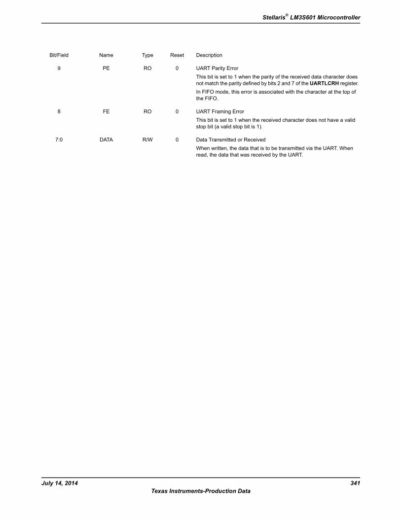
DescriptionResetTypeNameBit/Field
UART Parity ErrorThis bit is set to 1 when the parity of the received data character doesnot match the parity defined by bits 2 and 7 of the UARTLCRH register.In FIFO mode, this error is associated with the character at the top ofthe FIFO.
0ROPE9
UART Framing ErrorThis bit is set to 1 when the received character does not have a validstop bit (a valid stop bit is 1).
0ROFE8
Data Transmitted or ReceivedWhen written, the data that is to be transmitted via the UART. Whenread, the data that was received by the UART.
0R/WDATA7:0
341July 14, 2014Texas Instruments-Production Data
Stellaris® LM3S601 Microcontroller
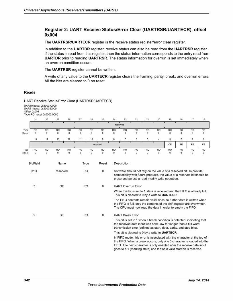
Register 2: UART Receive Status/Error Clear (UARTRSR/UARTECR), offset0x004The UARTRSR/UARTECR register is the receive status register/error clear register.
In addition to the UARTDR register, receive status can also be read from the UARTRSR register.If the status is read from this register, then the status information corresponds to the entry read fromUARTDR prior to reading UARTRSR. The status information for overrun is set immediately whenan overrun condition occurs.
The UARTRSR register cannot be written.
A write of any value to the UARTECR register clears the framing, parity, break, and overrun errors.All the bits are cleared to 0 on reset.
Reads
UART Receive Status/Error Clear (UARTRSR/UARTECR)UART0 base: 0x4000.C000UART1 base: 0x4000.D000Offset 0x004Type RO, reset 0x0000.0000
16171819202122232425262728293031
reserved
ROROROROROROROROROROROROROROROROType0000000000000000Reset
0123456789101112131415
FEPEBEOEreserved
ROROROROROROROROROROROROROROROROType0000000000000000Reset
DescriptionResetTypeNameBit/Field
Software should not rely on the value of a reserved bit. To providecompatibility with future products, the value of a reserved bit should bepreserved across a read-modify-write operation.
0ROreserved31:4
UART Overrun ErrorWhen this bit is set to 1, data is received and the FIFO is already full.This bit is cleared to 0 by a write to UARTECR.The FIFO contents remain valid since no further data is written whenthe FIFO is full, only the contents of the shift register are overwritten.The CPU must now read the data in order to empty the FIFO.
0ROOE3
UART Break ErrorThis bit is set to 1 when a break condition is detected, indicating thatthe received data input was held Low for longer than a full-wordtransmission time (defined as start, data, parity, and stop bits).This bit is cleared to 0 by a write to UARTECR.In FIFO mode, this error is associated with the character at the top ofthe FIFO. When a break occurs, only one 0 character is loaded into theFIFO. The next character is only enabled after the receive data inputgoes to a 1 (marking state) and the next valid start bit is received.
0ROBE2
July 14, 2014342Texas Instruments-Production Data
Universal Asynchronous Receivers/Transmitters (UARTs)
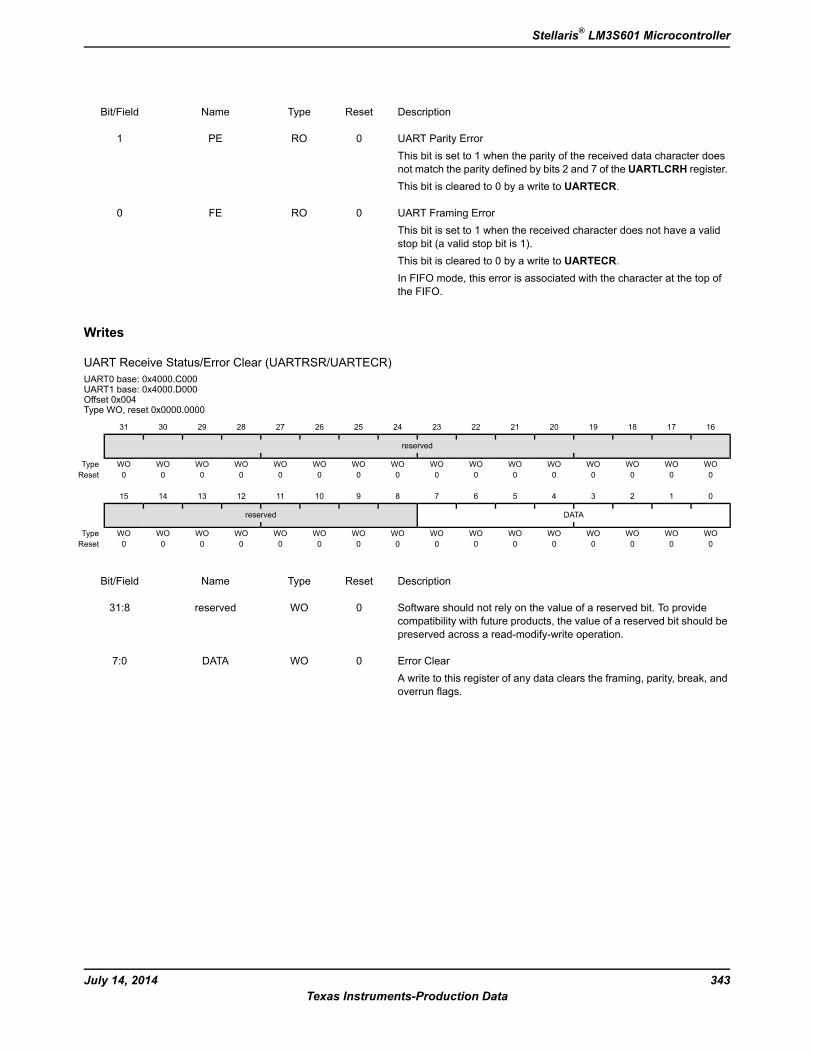
DescriptionResetTypeNameBit/Field
UART Parity ErrorThis bit is set to 1 when the parity of the received data character doesnot match the parity defined by bits 2 and 7 of the UARTLCRH register.This bit is cleared to 0 by a write to UARTECR.
0ROPE1
UART Framing ErrorThis bit is set to 1 when the received character does not have a validstop bit (a valid stop bit is 1).This bit is cleared to 0 by a write to UARTECR.In FIFO mode, this error is associated with the character at the top ofthe FIFO.
0ROFE0
Writes
UART Receive Status/Error Clear (UARTRSR/UARTECR)UART0 base: 0x4000.C000UART1 base: 0x4000.D000Offset 0x004Type WO, reset 0x0000.0000
16171819202122232425262728293031
reserved
WOWOWOWOWOWOWOWOWOWOWOWOWOWOWOWOType0000000000000000Reset
0123456789101112131415
DATAreserved
WOWOWOWOWOWOWOWOWOWOWOWOWOWOWOWOType0000000000000000Reset
DescriptionResetTypeNameBit/Field
Software should not rely on the value of a reserved bit. To providecompatibility with future products, the value of a reserved bit should bepreserved across a read-modify-write operation.
0WOreserved31:8
Error ClearA write to this register of any data clears the framing, parity, break, andoverrun flags.
0WODATA7:0
343July 14, 2014Texas Instruments-Production Data
Stellaris® LM3S601 Microcontroller
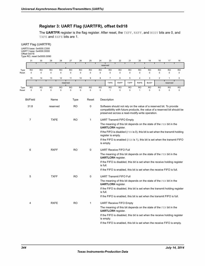
Register 3: UART Flag (UARTFR), offset 0x018The UARTFR register is the flag register. After reset, the TXFF, RXFF, and BUSY bits are 0, andTXFE and RXFE bits are 1.
UART Flag (UARTFR)UART0 base: 0x4000.C000UART1 base: 0x4000.D000Offset 0x018Type RO, reset 0x0000.0090
16171819202122232425262728293031
reserved
ROROROROROROROROROROROROROROROROType0000000000000000Reset
0123456789101112131415
reservedBUSYRXFETXFFRXFFTXFEreserved
ROROROROROROROROROROROROROROROROType0000100100000000Reset
DescriptionResetTypeNameBit/Field
Software should not rely on the value of a reserved bit. To providecompatibility with future products, the value of a reserved bit should bepreserved across a read-modify-write operation.
0ROreserved31:8
UART Transmit FIFO EmptyThe meaning of this bit depends on the state of the FEN bit in theUARTLCRH register.If the FIFO is disabled (FEN is 0), this bit is set when the transmit holdingregister is empty.If the FIFO is enabled (FEN is 1), this bit is set when the transmit FIFOis empty.
1ROTXFE7
UART Receive FIFO FullThe meaning of this bit depends on the state of the FEN bit in theUARTLCRH register.If the FIFO is disabled, this bit is set when the receive holding registeris full.If the FIFO is enabled, this bit is set when the receive FIFO is full.
0RORXFF6
UART Transmit FIFO FullThe meaning of this bit depends on the state of the FEN bit in theUARTLCRH register.If the FIFO is disabled, this bit is set when the transmit holding registeris full.If the FIFO is enabled, this bit is set when the transmit FIFO is full.
0ROTXFF5
UART Receive FIFO EmptyThe meaning of this bit depends on the state of the FEN bit in theUARTLCRH register.If the FIFO is disabled, this bit is set when the receive holding registeris empty.If the FIFO is enabled, this bit is set when the receive FIFO is empty.
1RORXFE4
July 14, 2014344Texas Instruments-Production Data
Universal Asynchronous Receivers/Transmitters (UARTs)
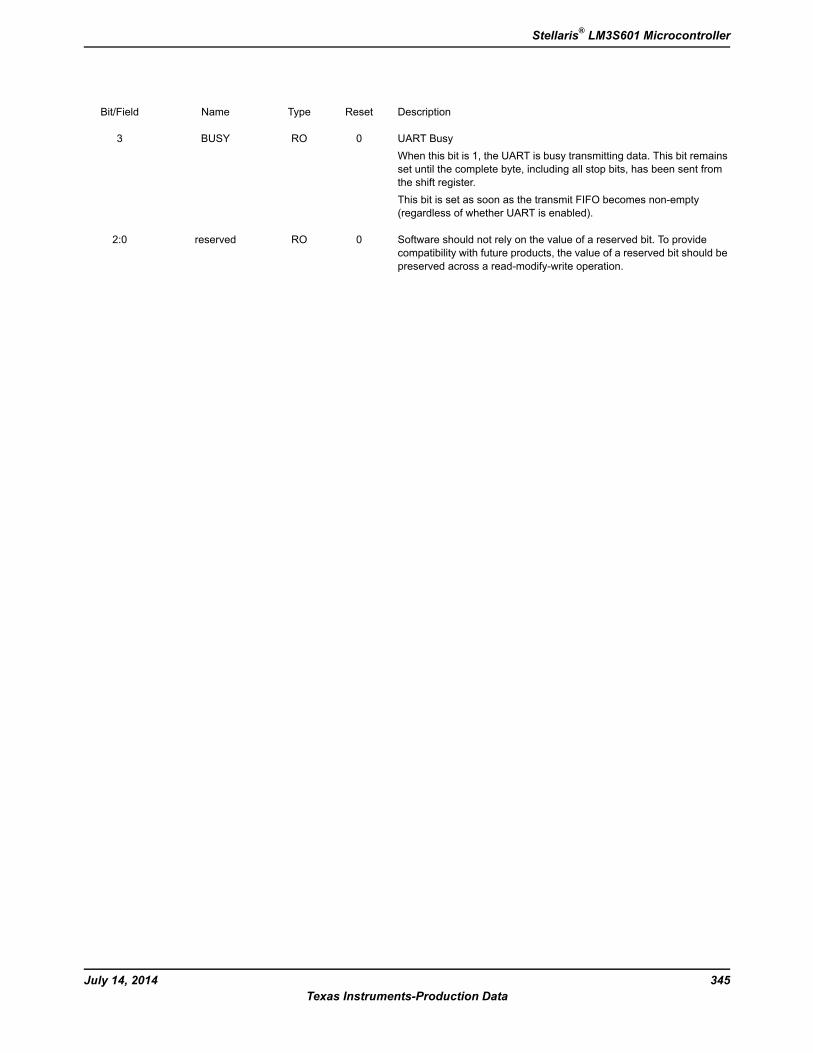
DescriptionResetTypeNameBit/Field
UART BusyWhen this bit is 1, the UART is busy transmitting data. This bit remainsset until the complete byte, including all stop bits, has been sent fromthe shift register.This bit is set as soon as the transmit FIFO becomes non-empty(regardless of whether UART is enabled).
0ROBUSY3
Software should not rely on the value of a reserved bit. To providecompatibility with future products, the value of a reserved bit should bepreserved across a read-modify-write operation.
0ROreserved2:0
345July 14, 2014Texas Instruments-Production Data
Stellaris® LM3S601 Microcontroller
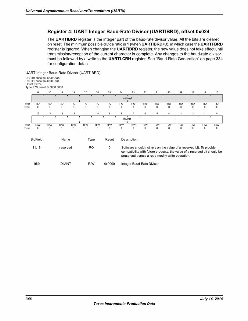
Register 4: UART Integer Baud-Rate Divisor (UARTIBRD), offset 0x024The UARTIBRD register is the integer part of the baud-rate divisor value. All the bits are clearedon reset. Theminimum possible divide ratio is 1 (whenUARTIBRD=0), in which case theUARTFBRDregister is ignored. When changing the UARTIBRD register, the new value does not take effect untiltransmission/reception of the current character is complete. Any changes to the baud-rate divisormust be followed by a write to the UARTLCRH register. See “Baud-Rate Generation” on page 334for configuration details.
UART Integer Baud-Rate Divisor (UARTIBRD)UART0 base: 0x4000.C000UART1 base: 0x4000.D000Offset 0x024Type R/W, reset 0x0000.0000
16171819202122232425262728293031
reserved
ROROROROROROROROROROROROROROROROType0000000000000000Reset
0123456789101112131415
DIVINT
R/WR/WR/WR/WR/WR/WR/WR/WR/WR/WR/WR/WR/WR/WR/WR/WType0000000000000000Reset
DescriptionResetTypeNameBit/Field
Software should not rely on the value of a reserved bit. To providecompatibility with future products, the value of a reserved bit should bepreserved across a read-modify-write operation.
0ROreserved31:16
Integer Baud-Rate Divisor0x0000R/WDIVINT15:0
July 14, 2014346Texas Instruments-Production Data
Universal Asynchronous Receivers/Transmitters (UARTs)
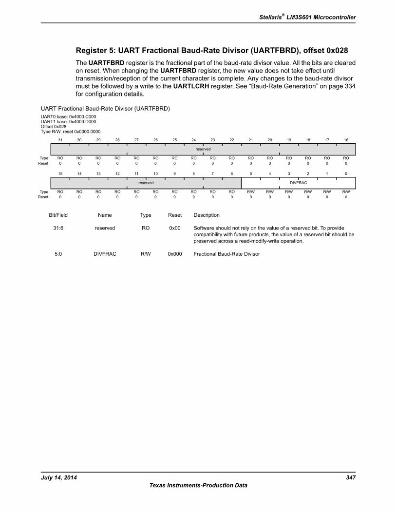
Register 5: UART Fractional Baud-Rate Divisor (UARTFBRD), offset 0x028The UARTFBRD register is the fractional part of the baud-rate divisor value. All the bits are clearedon reset. When changing the UARTFBRD register, the new value does not take effect untiltransmission/reception of the current character is complete. Any changes to the baud-rate divisormust be followed by a write to the UARTLCRH register. See “Baud-Rate Generation” on page 334for configuration details.
UART Fractional Baud-Rate Divisor (UARTFBRD)UART0 base: 0x4000.C000UART1 base: 0x4000.D000Offset 0x028Type R/W, reset 0x0000.0000
16171819202122232425262728293031
reserved
ROROROROROROROROROROROROROROROROType0000000000000000Reset
0123456789101112131415
DIVFRACreserved
R/WR/WR/WR/WR/WR/WROROROROROROROROROROType0000000000000000Reset
DescriptionResetTypeNameBit/Field
Software should not rely on the value of a reserved bit. To providecompatibility with future products, the value of a reserved bit should bepreserved across a read-modify-write operation.
0x00ROreserved31:6
Fractional Baud-Rate Divisor0x000R/WDIVFRAC5:0
347July 14, 2014Texas Instruments-Production Data
Stellaris® LM3S601 Microcontroller
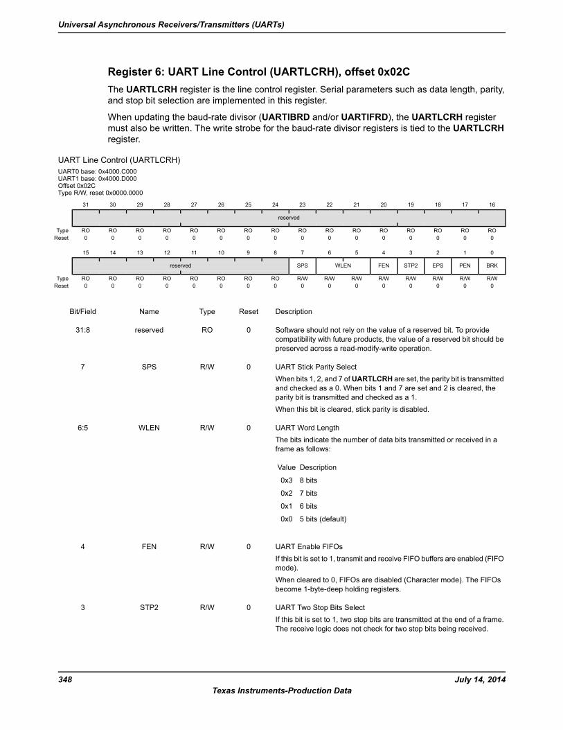
Register 6: UART Line Control (UARTLCRH), offset 0x02CThe UARTLCRH register is the line control register. Serial parameters such as data length, parity,and stop bit selection are implemented in this register.
When updating the baud-rate divisor (UARTIBRD and/or UARTIFRD), the UARTLCRH registermust also be written. The write strobe for the baud-rate divisor registers is tied to the UARTLCRHregister.
UART Line Control (UARTLCRH)UART0 base: 0x4000.C000UART1 base: 0x4000.D000Offset 0x02CType R/W, reset 0x0000.0000
16171819202122232425262728293031
reserved
ROROROROROROROROROROROROROROROROType0000000000000000Reset
0123456789101112131415
BRKPENEPSSTP2FENWLENSPSreserved
R/WR/WR/WR/WR/WR/WR/WR/WROROROROROROROROType0000000000000000Reset
DescriptionResetTypeNameBit/Field
Software should not rely on the value of a reserved bit. To providecompatibility with future products, the value of a reserved bit should bepreserved across a read-modify-write operation.
0ROreserved31:8
UART Stick Parity SelectWhen bits 1, 2, and 7 ofUARTLCRH are set, the parity bit is transmittedand checked as a 0. When bits 1 and 7 are set and 2 is cleared, theparity bit is transmitted and checked as a 1.When this bit is cleared, stick parity is disabled.
0R/WSPS7
UART Word LengthThe bits indicate the number of data bits transmitted or received in aframe as follows:
DescriptionValue
8 bits0x3
7 bits0x2
6 bits0x1
5 bits (default)0x0
0R/WWLEN6:5
UART Enable FIFOsIf this bit is set to 1, transmit and receive FIFO buffers are enabled (FIFOmode).When cleared to 0, FIFOs are disabled (Character mode). The FIFOsbecome 1-byte-deep holding registers.
0R/WFEN4
UART Two Stop Bits SelectIf this bit is set to 1, two stop bits are transmitted at the end of a frame.The receive logic does not check for two stop bits being received.
0R/WSTP23
July 14, 2014348Texas Instruments-Production Data
Universal Asynchronous Receivers/Transmitters (UARTs)
DescriptionResetTypeNameBit/Field
UART Even Parity SelectIf this bit is set to 1, even parity generation and checking is performedduring transmission and reception, which checks for an even numberof 1s in data and parity bits.When cleared to 0, then odd parity is performed, which checks for anodd number of 1s.This bit has no effect when parity is disabled by the PEN bit.
0R/WEPS2
UART Parity EnableIf this bit is set to 1, parity checking and generation is enabled; otherwise,parity is disabled and no parity bit is added to the data frame.
0R/WPEN1
UART Send BreakIf this bit is set to 1, a Low level is continually output on the UnTX output,after completing transmission of the current character. For the properexecution of the break command, the software must set this bit for atleast two frames (character periods). For normal use, this bit must becleared to 0.
0R/WBRK0
349July 14, 2014Texas Instruments-Production Data
Stellaris® LM3S601 Microcontroller
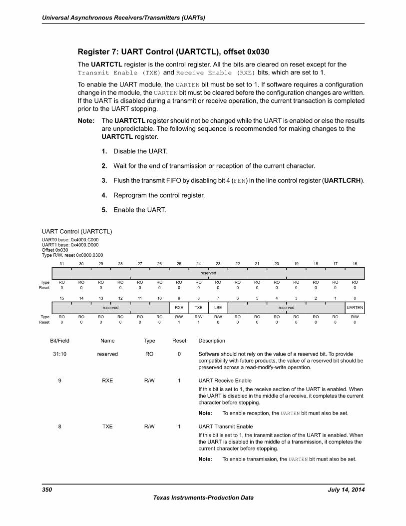
Register 7: UART Control (UARTCTL), offset 0x030The UARTCTL register is the control register. All the bits are cleared on reset except for theTransmit Enable (TXE) and Receive Enable (RXE) bits, which are set to 1.
To enable the UART module, the UARTEN bit must be set to 1. If software requires a configurationchange in the module, the UARTEN bit must be cleared before the configuration changes are written.If the UART is disabled during a transmit or receive operation, the current transaction is completedprior to the UART stopping.
Note: TheUARTCTL register should not be changed while the UART is enabled or else the resultsare unpredictable. The following sequence is recommended for making changes to theUARTCTL register.
1. Disable the UART.
2. Wait for the end of transmission or reception of the current character.
3. Flush the transmit FIFO by disabling bit 4 (FEN) in the line control register (UARTLCRH).
4. Reprogram the control register.
5. Enable the UART.
UART Control (UARTCTL)UART0 base: 0x4000.C000UART1 base: 0x4000.D000Offset 0x030Type R/W, reset 0x0000.0300
16171819202122232425262728293031
reserved
ROROROROROROROROROROROROROROROROType0000000000000000Reset
0123456789101112131415
UARTENreservedLBETXERXEreserved
R/WROROROROROROR/WR/WR/WROROROROROROType0000000011000000Reset
DescriptionResetTypeNameBit/Field
Software should not rely on the value of a reserved bit. To providecompatibility with future products, the value of a reserved bit should bepreserved across a read-modify-write operation.
0ROreserved31:10
UART Receive EnableIf this bit is set to 1, the receive section of the UART is enabled. Whenthe UART is disabled in the middle of a receive, it completes the currentcharacter before stopping.
Note: To enable reception, the UARTEN bit must also be set.
1R/WRXE9
UART Transmit EnableIf this bit is set to 1, the transmit section of the UART is enabled. Whenthe UART is disabled in the middle of a transmission, it completes thecurrent character before stopping.
Note: To enable transmission, the UARTEN bit must also be set.
1R/WTXE8
July 14, 2014350Texas Instruments-Production Data
Universal Asynchronous Receivers/Transmitters (UARTs)
DescriptionResetTypeNameBit/Field
UART Loop Back EnableIf this bit is set to 1, the UnTX path is fed through the UnRX path.
0R/WLBE7
Software should not rely on the value of a reserved bit. To providecompatibility with future products, the value of a reserved bit should bepreserved across a read-modify-write operation.
0ROreserved6:1
UART EnableIf this bit is set to 1, the UART is enabled. When the UART is disabledin the middle of transmission or reception, it completes the currentcharacter before stopping.
0R/WUARTEN0
351July 14, 2014Texas Instruments-Production Data
Stellaris® LM3S601 Microcontroller
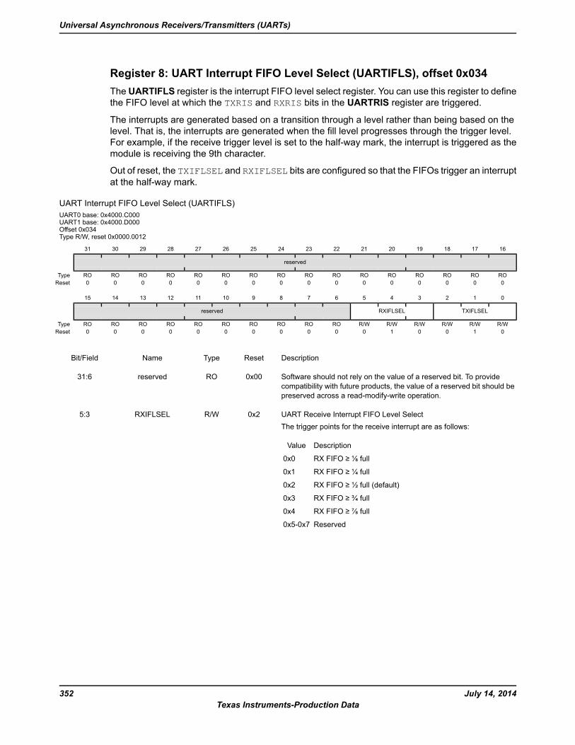
Register 8: UART Interrupt FIFO Level Select (UARTIFLS), offset 0x034The UARTIFLS register is the interrupt FIFO level select register. You can use this register to definethe FIFO level at which the TXRIS and RXRIS bits in the UARTRIS register are triggered.
The interrupts are generated based on a transition through a level rather than being based on thelevel. That is, the interrupts are generated when the fill level progresses through the trigger level.For example, if the receive trigger level is set to the half-way mark, the interrupt is triggered as themodule is receiving the 9th character.
Out of reset, the TXIFLSEL and RXIFLSEL bits are configured so that the FIFOs trigger an interruptat the half-way mark.
UART Interrupt FIFO Level Select (UARTIFLS)UART0 base: 0x4000.C000UART1 base: 0x4000.D000Offset 0x034Type R/W, reset 0x0000.0012
16171819202122232425262728293031
reserved
ROROROROROROROROROROROROROROROROType0000000000000000Reset
0123456789101112131415
TXIFLSELRXIFLSELreserved
R/WR/WR/WR/WR/WR/WROROROROROROROROROROType0100100000000000Reset
DescriptionResetTypeNameBit/Field
Software should not rely on the value of a reserved bit. To providecompatibility with future products, the value of a reserved bit should bepreserved across a read-modify-write operation.
0x00ROreserved31:6
UART Receive Interrupt FIFO Level SelectThe trigger points for the receive interrupt are as follows:
DescriptionValue
RX FIFO ≥ ⅛ full0x0
RX FIFO ≥ ¼ full0x1
RX FIFO ≥ ½ full (default)0x2
RX FIFO ≥ ¾ full0x3
RX FIFO ≥ ⅞ full0x4
Reserved0x5-0x7
0x2R/WRXIFLSEL5:3
July 14, 2014352Texas Instruments-Production Data
Universal Asynchronous Receivers/Transmitters (UARTs)
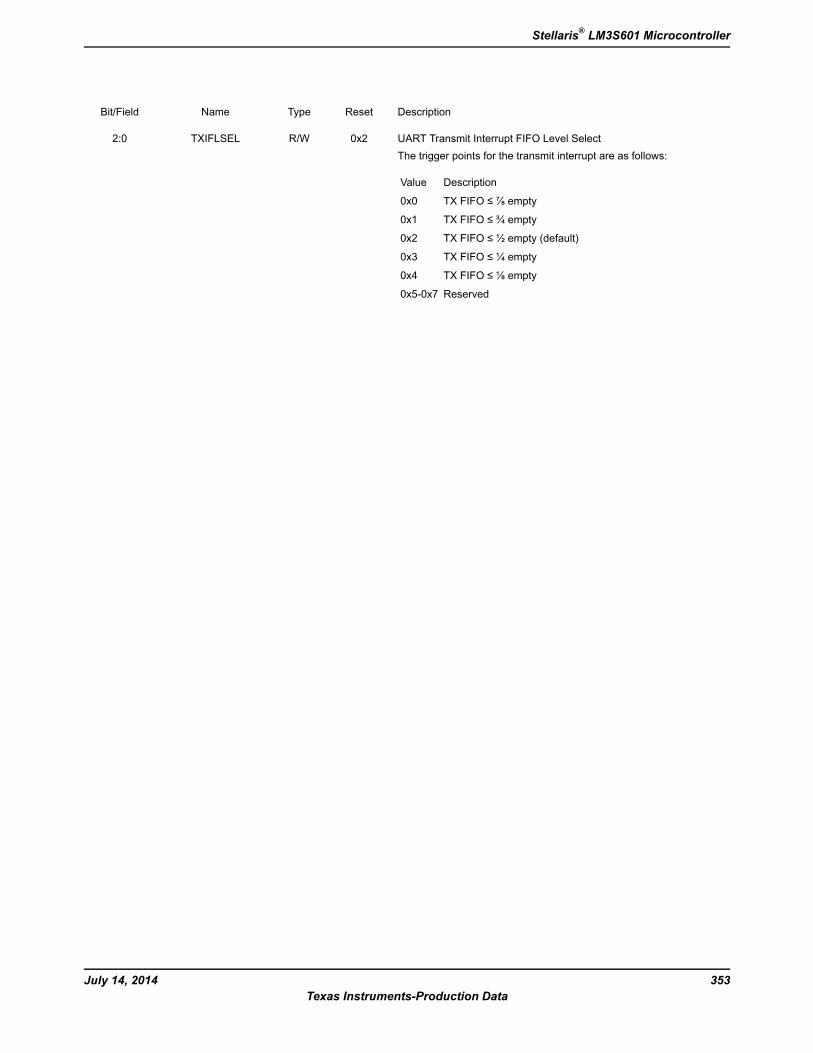
DescriptionResetTypeNameBit/Field
UART Transmit Interrupt FIFO Level SelectThe trigger points for the transmit interrupt are as follows:
DescriptionValue
TX FIFO ≤ ⅞ empty0x0
TX FIFO ≤ ¾ empty0x1
TX FIFO ≤ ½ empty (default)0x2
TX FIFO ≤ ¼ empty0x3
TX FIFO ≤ ⅛ empty0x4
Reserved0x5-0x7
0x2R/WTXIFLSEL2:0
353July 14, 2014Texas Instruments-Production Data
Stellaris® LM3S601 Microcontroller
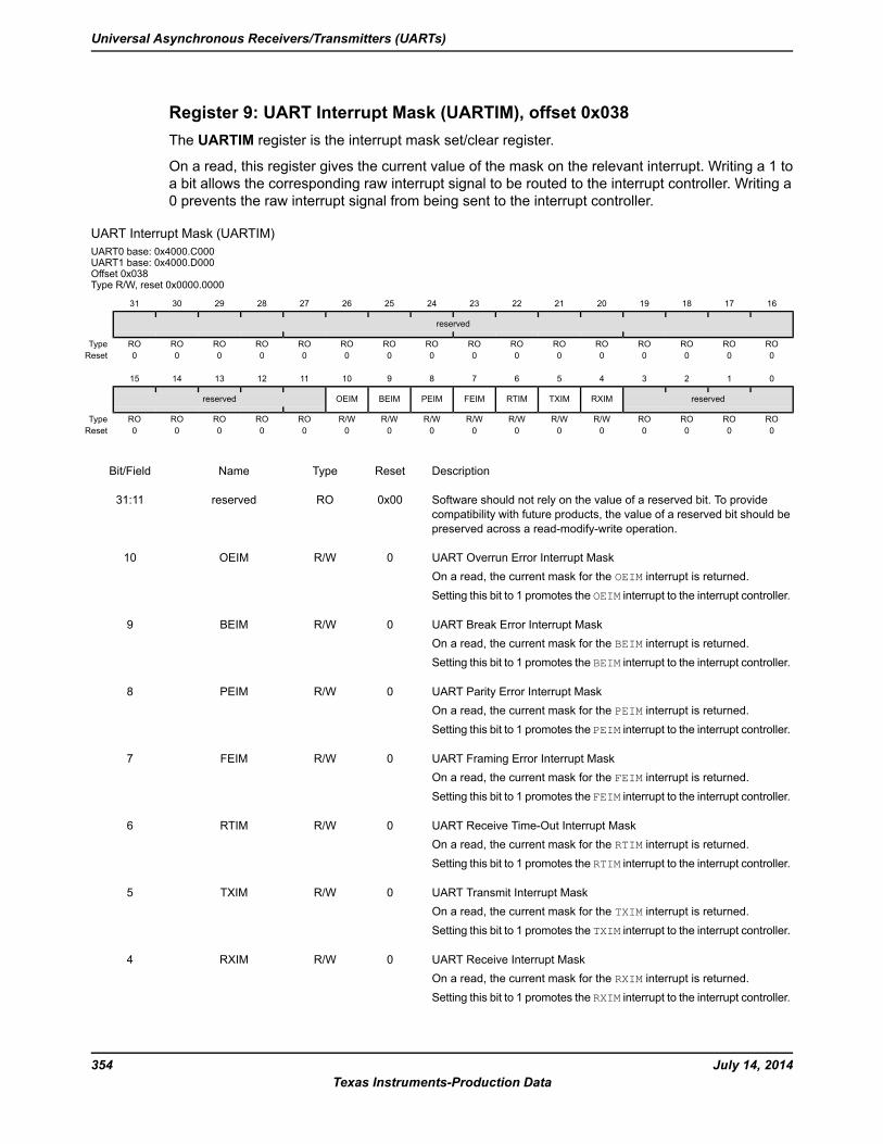
Register 9: UART Interrupt Mask (UARTIM), offset 0x038The UARTIM register is the interrupt mask set/clear register.
On a read, this register gives the current value of the mask on the relevant interrupt. Writing a 1 toa bit allows the corresponding raw interrupt signal to be routed to the interrupt controller. Writing a0 prevents the raw interrupt signal from being sent to the interrupt controller.
UART Interrupt Mask (UARTIM)UART0 base: 0x4000.C000UART1 base: 0x4000.D000Offset 0x038Type R/W, reset 0x0000.0000
16171819202122232425262728293031
reserved
ROROROROROROROROROROROROROROROROType0000000000000000Reset
0123456789101112131415
reservedRXIMTXIMRTIMFEIMPEIMBEIMOEIMreserved
ROROROROR/WR/WR/WR/WR/WR/WR/WROROROROROType0000000000000000Reset
DescriptionResetTypeNameBit/Field
Software should not rely on the value of a reserved bit. To providecompatibility with future products, the value of a reserved bit should bepreserved across a read-modify-write operation.
0x00ROreserved31:11
UART Overrun Error Interrupt MaskOn a read, the current mask for the OEIM interrupt is returned.Setting this bit to 1 promotes the OEIM interrupt to the interrupt controller.
0R/WOEIM10
UART Break Error Interrupt MaskOn a read, the current mask for the BEIM interrupt is returned.Setting this bit to 1 promotes the BEIM interrupt to the interrupt controller.
0R/WBEIM9
UART Parity Error Interrupt MaskOn a read, the current mask for the PEIM interrupt is returned.Setting this bit to 1 promotes the PEIM interrupt to the interrupt controller.
0R/WPEIM8
UART Framing Error Interrupt MaskOn a read, the current mask for the FEIM interrupt is returned.Setting this bit to 1 promotes the FEIM interrupt to the interrupt controller.
0R/WFEIM7
UART Receive Time-Out Interrupt MaskOn a read, the current mask for the RTIM interrupt is returned.Setting this bit to 1 promotes the RTIM interrupt to the interrupt controller.
0R/WRTIM6
UART Transmit Interrupt MaskOn a read, the current mask for the TXIM interrupt is returned.Setting this bit to 1 promotes the TXIM interrupt to the interrupt controller.
0R/WTXIM5
UART Receive Interrupt MaskOn a read, the current mask for the RXIM interrupt is returned.Setting this bit to 1 promotes the RXIM interrupt to the interrupt controller.
0R/WRXIM4
July 14, 2014354Texas Instruments-Production Data
Universal Asynchronous Receivers/Transmitters (UARTs)
DescriptionResetTypeNameBit/Field
Software should not rely on the value of a reserved bit. To providecompatibility with future products, the value of a reserved bit should bepreserved across a read-modify-write operation.
0x00ROreserved3:0
355July 14, 2014Texas Instruments-Production Data
Stellaris® LM3S601 Microcontroller
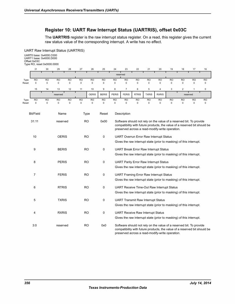
Register 10: UART Raw Interrupt Status (UARTRIS), offset 0x03CThe UARTRIS register is the raw interrupt status register. On a read, this register gives the currentraw status value of the corresponding interrupt. A write has no effect.
UART Raw Interrupt Status (UARTRIS)UART0 base: 0x4000.C000UART1 base: 0x4000.D000Offset 0x03CType RO, reset 0x0000.0000
16171819202122232425262728293031
reserved
ROROROROROROROROROROROROROROROROType0000000000000000Reset
0123456789101112131415
reservedRXRISTXRISRTRISFERISPERISBERISOERISreserved
ROROROROROROROROROROROROROROROROType0000000000000000Reset
DescriptionResetTypeNameBit/Field
Software should not rely on the value of a reserved bit. To providecompatibility with future products, the value of a reserved bit should bepreserved across a read-modify-write operation.
0x00ROreserved31:11
UART Overrun Error Raw Interrupt StatusGives the raw interrupt state (prior to masking) of this interrupt.
0ROOERIS10
UART Break Error Raw Interrupt StatusGives the raw interrupt state (prior to masking) of this interrupt.
0ROBERIS9
UART Parity Error Raw Interrupt StatusGives the raw interrupt state (prior to masking) of this interrupt.
0ROPERIS8
UART Framing Error Raw Interrupt StatusGives the raw interrupt state (prior to masking) of this interrupt.
0ROFERIS7
UART Receive Time-Out Raw Interrupt StatusGives the raw interrupt state (prior to masking) of this interrupt.
0RORTRIS6
UART Transmit Raw Interrupt StatusGives the raw interrupt state (prior to masking) of this interrupt.
0ROTXRIS5
UART Receive Raw Interrupt StatusGives the raw interrupt state (prior to masking) of this interrupt.
0RORXRIS4
Software should not rely on the value of a reserved bit. To providecompatibility with future products, the value of a reserved bit should bepreserved across a read-modify-write operation.
0x0ROreserved3:0
July 14, 2014356Texas Instruments-Production Data
Universal Asynchronous Receivers/Transmitters (UARTs)
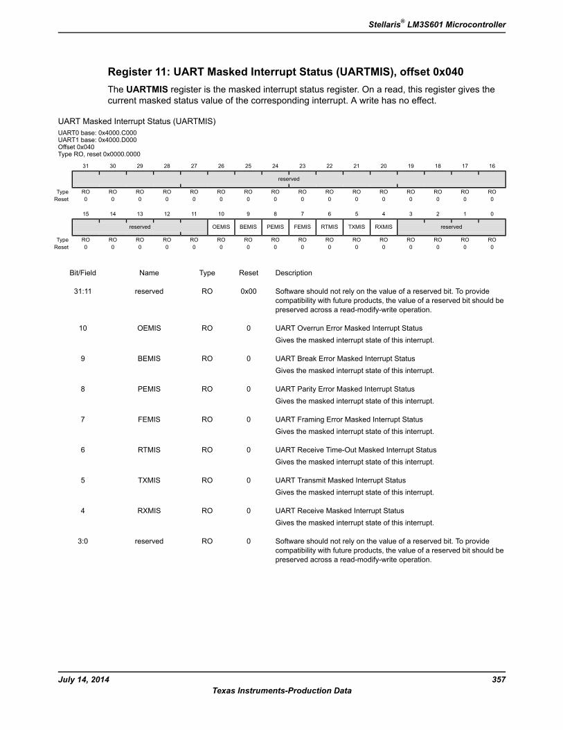
Register 11: UART Masked Interrupt Status (UARTMIS), offset 0x040The UARTMIS register is the masked interrupt status register. On a read, this register gives thecurrent masked status value of the corresponding interrupt. A write has no effect.
UART Masked Interrupt Status (UARTMIS)UART0 base: 0x4000.C000UART1 base: 0x4000.D000Offset 0x040Type RO, reset 0x0000.0000
16171819202122232425262728293031
reserved
ROROROROROROROROROROROROROROROROType0000000000000000Reset
0123456789101112131415
reservedRXMISTXMISRTMISFEMISPEMISBEMISOEMISreserved
ROROROROROROROROROROROROROROROROType0000000000000000Reset
DescriptionResetTypeNameBit/Field
Software should not rely on the value of a reserved bit. To providecompatibility with future products, the value of a reserved bit should bepreserved across a read-modify-write operation.
0x00ROreserved31:11
UART Overrun Error Masked Interrupt StatusGives the masked interrupt state of this interrupt.
0ROOEMIS10
UART Break Error Masked Interrupt StatusGives the masked interrupt state of this interrupt.
0ROBEMIS9
UART Parity Error Masked Interrupt StatusGives the masked interrupt state of this interrupt.
0ROPEMIS8
UART Framing Error Masked Interrupt StatusGives the masked interrupt state of this interrupt.
0ROFEMIS7
UART Receive Time-Out Masked Interrupt StatusGives the masked interrupt state of this interrupt.
0RORTMIS6
UART Transmit Masked Interrupt StatusGives the masked interrupt state of this interrupt.
0ROTXMIS5
UART Receive Masked Interrupt StatusGives the masked interrupt state of this interrupt.
0RORXMIS4
Software should not rely on the value of a reserved bit. To providecompatibility with future products, the value of a reserved bit should bepreserved across a read-modify-write operation.
0ROreserved3:0
357July 14, 2014Texas Instruments-Production Data
Stellaris® LM3S601 Microcontroller
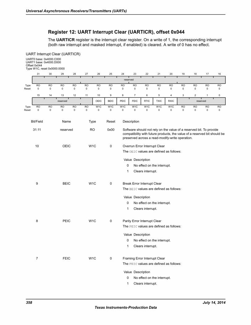
Register 12: UART Interrupt Clear (UARTICR), offset 0x044The UARTICR register is the interrupt clear register. On a write of 1, the corresponding interrupt(both raw interrupt and masked interrupt, if enabled) is cleared. A write of 0 has no effect.
UART Interrupt Clear (UARTICR)UART0 base: 0x4000.C000UART1 base: 0x4000.D000Offset 0x044Type W1C, reset 0x0000.0000
16171819202122232425262728293031
reserved
ROROROROROROROROROROROROROROROROType0000000000000000Reset
0123456789101112131415
reservedRXICTXICRTICFEICPEICBEICOEICreserved
ROROROROW1CW1CW1CW1CW1CW1CW1CROROROROROType0000000000000000Reset
DescriptionResetTypeNameBit/Field
Software should not rely on the value of a reserved bit. To providecompatibility with future products, the value of a reserved bit should bepreserved across a read-modify-write operation.
0x00ROreserved31:11
Overrun Error Interrupt ClearThe OEIC values are defined as follows:
DescriptionValue
No effect on the interrupt.0
Clears interrupt.1
0W1COEIC10
Break Error Interrupt ClearThe BEIC values are defined as follows:
DescriptionValue
No effect on the interrupt.0
Clears interrupt.1
0W1CBEIC9
Parity Error Interrupt ClearThe PEIC values are defined as follows:
DescriptionValue
No effect on the interrupt.0
Clears interrupt.1
0W1CPEIC8
Framing Error Interrupt ClearThe FEIC values are defined as follows:
DescriptionValue
No effect on the interrupt.0
Clears interrupt.1
0W1CFEIC7
July 14, 2014358Texas Instruments-Production Data
Universal Asynchronous Receivers/Transmitters (UARTs)
DescriptionResetTypeNameBit/Field
Receive Time-Out Interrupt ClearThe RTIC values are defined as follows:
DescriptionValue
No effect on the interrupt.0
Clears interrupt.1
0W1CRTIC6
Transmit Interrupt ClearThe TXIC values are defined as follows:
DescriptionValue
No effect on the interrupt.0
Clears interrupt.1
0W1CTXIC5
Receive Interrupt ClearThe RXIC values are defined as follows:
DescriptionValue
No effect on the interrupt.0
Clears interrupt.1
0W1CRXIC4
Software should not rely on the value of a reserved bit. To providecompatibility with future products, the value of a reserved bit should bepreserved across a read-modify-write operation.
0x00ROreserved3:0
359July 14, 2014Texas Instruments-Production Data
Stellaris® LM3S601 Microcontroller

Register 13: UART Peripheral Identification 4 (UARTPeriphID4), offset 0xFD0The UARTPeriphIDn registers are hard-coded and the fields within the registers determine thereset values.
UART Peripheral Identification 4 (UARTPeriphID4)UART0 base: 0x4000.C000UART1 base: 0x4000.D000Offset 0xFD0Type RO, reset 0x0000.0000
16171819202122232425262728293031
reserved
ROROROROROROROROROROROROROROROROType0000000000000000Reset
0123456789101112131415
PID4reserved
ROROROROROROROROROROROROROROROROType0000000000000000Reset
DescriptionResetTypeNameBit/Field
Software should not rely on the value of a reserved bit. To providecompatibility with future products, the value of a reserved bit should bepreserved across a read-modify-write operation.
0x00ROreserved31:8
UART Peripheral ID Register[7:0]Can be used by software to identify the presence of this peripheral.
0x0000ROPID47:0
July 14, 2014360Texas Instruments-Production Data
Universal Asynchronous Receivers/Transmitters (UARTs)

Register 14: UART Peripheral Identification 5 (UARTPeriphID5), offset 0xFD4The UARTPeriphIDn registers are hard-coded and the fields within the registers determine thereset values.
UART Peripheral Identification 5 (UARTPeriphID5)UART0 base: 0x4000.C000UART1 base: 0x4000.D000Offset 0xFD4Type RO, reset 0x0000.0000
16171819202122232425262728293031
reserved
ROROROROROROROROROROROROROROROROType0000000000000000Reset
0123456789101112131415
PID5reserved
ROROROROROROROROROROROROROROROROType0000000000000000Reset
DescriptionResetTypeNameBit/Field
Software should not rely on the value of a reserved bit. To providecompatibility with future products, the value of a reserved bit should bepreserved across a read-modify-write operation.
0x00ROreserved31:8
UART Peripheral ID Register[15:8]Can be used by software to identify the presence of this peripheral.
0x0000ROPID57:0
361July 14, 2014Texas Instruments-Production Data
Stellaris® LM3S601 Microcontroller
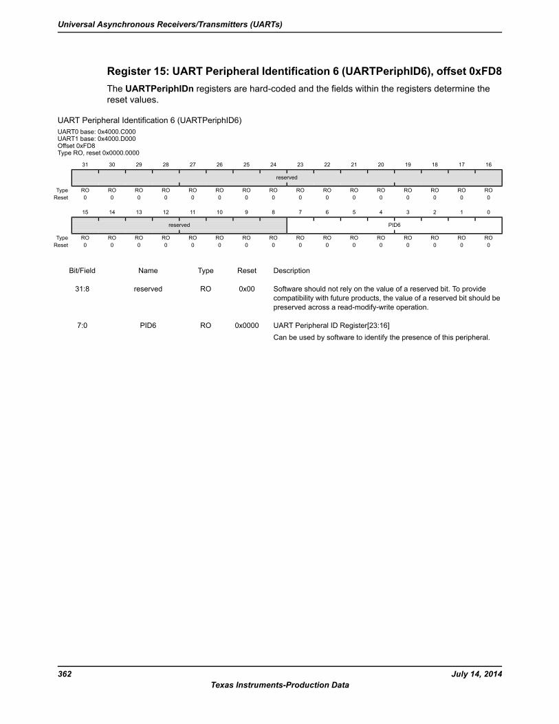
Register 15: UART Peripheral Identification 6 (UARTPeriphID6), offset 0xFD8The UARTPeriphIDn registers are hard-coded and the fields within the registers determine thereset values.
UART Peripheral Identification 6 (UARTPeriphID6)UART0 base: 0x4000.C000UART1 base: 0x4000.D000Offset 0xFD8Type RO, reset 0x0000.0000
16171819202122232425262728293031
reserved
ROROROROROROROROROROROROROROROROType0000000000000000Reset
0123456789101112131415
PID6reserved
ROROROROROROROROROROROROROROROROType0000000000000000Reset
DescriptionResetTypeNameBit/Field
Software should not rely on the value of a reserved bit. To providecompatibility with future products, the value of a reserved bit should bepreserved across a read-modify-write operation.
0x00ROreserved31:8
UART Peripheral ID Register[23:16]Can be used by software to identify the presence of this peripheral.
0x0000ROPID67:0
July 14, 2014362Texas Instruments-Production Data
Universal Asynchronous Receivers/Transmitters (UARTs)

Register 16: UART Peripheral Identification 7 (UARTPeriphID7), offset 0xFDCThe UARTPeriphIDn registers are hard-coded and the fields within the registers determine thereset values.
UART Peripheral Identification 7 (UARTPeriphID7)UART0 base: 0x4000.C000UART1 base: 0x4000.D000Offset 0xFDCType RO, reset 0x0000.0000
16171819202122232425262728293031
reserved
ROROROROROROROROROROROROROROROROType0000000000000000Reset
0123456789101112131415
PID7reserved
ROROROROROROROROROROROROROROROROType0000000000000000Reset
DescriptionResetTypeNameBit/Field
Software should not rely on the value of a reserved bit. To providecompatibility with future products, the value of a reserved bit should bepreserved across a read-modify-write operation.
0ROreserved31:8
UART Peripheral ID Register[31:24]Can be used by software to identify the presence of this peripheral.
0x0000ROPID77:0
363July 14, 2014Texas Instruments-Production Data
Stellaris® LM3S601 Microcontroller

Register 17: UART Peripheral Identification 0 (UARTPeriphID0), offset 0xFE0The UARTPeriphIDn registers are hard-coded and the fields within the registers determine thereset values.
UART Peripheral Identification 0 (UARTPeriphID0)UART0 base: 0x4000.C000UART1 base: 0x4000.D000Offset 0xFE0Type RO, reset 0x0000.0011
16171819202122232425262728293031
reserved
ROROROROROROROROROROROROROROROROType0000000000000000Reset
0123456789101112131415
PID0reserved
ROROROROROROROROROROROROROROROROType1000100000000000Reset
DescriptionResetTypeNameBit/Field
Software should not rely on the value of a reserved bit. To providecompatibility with future products, the value of a reserved bit should bepreserved across a read-modify-write operation.
0x00ROreserved31:8
UART Peripheral ID Register[7:0]Can be used by software to identify the presence of this peripheral.
0x11ROPID07:0
July 14, 2014364Texas Instruments-Production Data
Universal Asynchronous Receivers/Transmitters (UARTs)
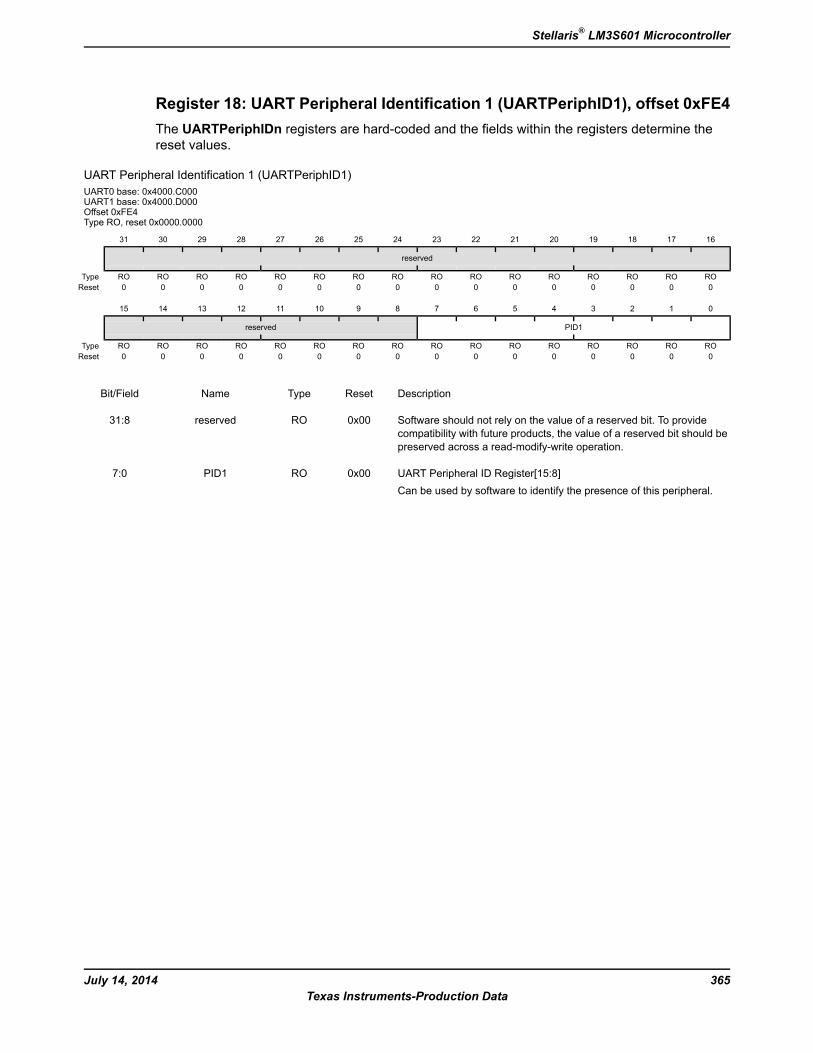
Register 18: UART Peripheral Identification 1 (UARTPeriphID1), offset 0xFE4The UARTPeriphIDn registers are hard-coded and the fields within the registers determine thereset values.
UART Peripheral Identification 1 (UARTPeriphID1)UART0 base: 0x4000.C000UART1 base: 0x4000.D000Offset 0xFE4Type RO, reset 0x0000.0000
16171819202122232425262728293031
reserved
ROROROROROROROROROROROROROROROROType0000000000000000Reset
0123456789101112131415
PID1reserved
ROROROROROROROROROROROROROROROROType0000000000000000Reset
DescriptionResetTypeNameBit/Field
Software should not rely on the value of a reserved bit. To providecompatibility with future products, the value of a reserved bit should bepreserved across a read-modify-write operation.
0x00ROreserved31:8
UART Peripheral ID Register[15:8]Can be used by software to identify the presence of this peripheral.
0x00ROPID17:0
365July 14, 2014Texas Instruments-Production Data
Stellaris® LM3S601 Microcontroller

Register 19: UART Peripheral Identification 2 (UARTPeriphID2), offset 0xFE8The UARTPeriphIDn registers are hard-coded and the fields within the registers determine thereset values.
UART Peripheral Identification 2 (UARTPeriphID2)UART0 base: 0x4000.C000UART1 base: 0x4000.D000Offset 0xFE8Type RO, reset 0x0000.0018
16171819202122232425262728293031
reserved
ROROROROROROROROROROROROROROROROType0000000000000000Reset
0123456789101112131415
PID2reserved
ROROROROROROROROROROROROROROROROType0001100000000000Reset
DescriptionResetTypeNameBit/Field
Software should not rely on the value of a reserved bit. To providecompatibility with future products, the value of a reserved bit should bepreserved across a read-modify-write operation.
0x00ROreserved31:8
UART Peripheral ID Register[23:16]Can be used by software to identify the presence of this peripheral.
0x18ROPID27:0
July 14, 2014366Texas Instruments-Production Data
Universal Asynchronous Receivers/Transmitters (UARTs)

Register 20: UART Peripheral Identification 3 (UARTPeriphID3), offset 0xFECThe UARTPeriphIDn registers are hard-coded and the fields within the registers determine thereset values.
UART Peripheral Identification 3 (UARTPeriphID3)UART0 base: 0x4000.C000UART1 base: 0x4000.D000Offset 0xFECType RO, reset 0x0000.0001
16171819202122232425262728293031
reserved
ROROROROROROROROROROROROROROROROType0000000000000000Reset
0123456789101112131415
PID3reserved
ROROROROROROROROROROROROROROROROType1000000000000000Reset
DescriptionResetTypeNameBit/Field
Software should not rely on the value of a reserved bit. To providecompatibility with future products, the value of a reserved bit should bepreserved across a read-modify-write operation.
0x00ROreserved31:8
UART Peripheral ID Register[31:24]Can be used by software to identify the presence of this peripheral.
0x01ROPID37:0
367July 14, 2014Texas Instruments-Production Data
Stellaris® LM3S601 Microcontroller
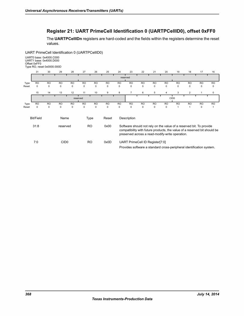
Register 21: UART PrimeCell Identification 0 (UARTPCellID0), offset 0xFF0The UARTPCellIDn registers are hard-coded and the fields within the registers determine the resetvalues.
UART PrimeCell Identification 0 (UARTPCellID0)UART0 base: 0x4000.C000UART1 base: 0x4000.D000Offset 0xFF0Type RO, reset 0x0000.000D
16171819202122232425262728293031
reserved
ROROROROROROROROROROROROROROROROType0000000000000000Reset
0123456789101112131415
CID0reserved
ROROROROROROROROROROROROROROROROType1011000000000000Reset
DescriptionResetTypeNameBit/Field
Software should not rely on the value of a reserved bit. To providecompatibility with future products, the value of a reserved bit should bepreserved across a read-modify-write operation.
0x00ROreserved31:8
UART PrimeCell ID Register[7:0]Provides software a standard cross-peripheral identification system.
0x0DROCID07:0
July 14, 2014368Texas Instruments-Production Data
Universal Asynchronous Receivers/Transmitters (UARTs)
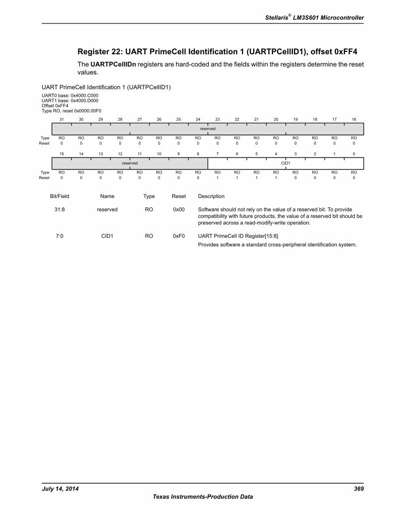
Register 22: UART PrimeCell Identification 1 (UARTPCellID1), offset 0xFF4The UARTPCellIDn registers are hard-coded and the fields within the registers determine the resetvalues.
UART PrimeCell Identification 1 (UARTPCellID1)UART0 base: 0x4000.C000UART1 base: 0x4000.D000Offset 0xFF4Type RO, reset 0x0000.00F0
16171819202122232425262728293031
reserved
ROROROROROROROROROROROROROROROROType0000000000000000Reset
0123456789101112131415
CID1reserved
ROROROROROROROROROROROROROROROROType0000111100000000Reset
DescriptionResetTypeNameBit/Field
Software should not rely on the value of a reserved bit. To providecompatibility with future products, the value of a reserved bit should bepreserved across a read-modify-write operation.
0x00ROreserved31:8
UART PrimeCell ID Register[15:8]Provides software a standard cross-peripheral identification system.
0xF0ROCID17:0
369July 14, 2014Texas Instruments-Production Data
Stellaris® LM3S601 Microcontroller

Register 23: UART PrimeCell Identification 2 (UARTPCellID2), offset 0xFF8The UARTPCellIDn registers are hard-coded and the fields within the registers determine the resetvalues.
UART PrimeCell Identification 2 (UARTPCellID2)UART0 base: 0x4000.C000UART1 base: 0x4000.D000Offset 0xFF8Type RO, reset 0x0000.0005
16171819202122232425262728293031
reserved
ROROROROROROROROROROROROROROROROType0000000000000000Reset
0123456789101112131415
CID2reserved
ROROROROROROROROROROROROROROROROType1010000000000000Reset
DescriptionResetTypeNameBit/Field
Software should not rely on the value of a reserved bit. To providecompatibility with future products, the value of a reserved bit should bepreserved across a read-modify-write operation.
0x00ROreserved31:8
UART PrimeCell ID Register[23:16]Provides software a standard cross-peripheral identification system.
0x05ROCID27:0
July 14, 2014370Texas Instruments-Production Data
Universal Asynchronous Receivers/Transmitters (UARTs)
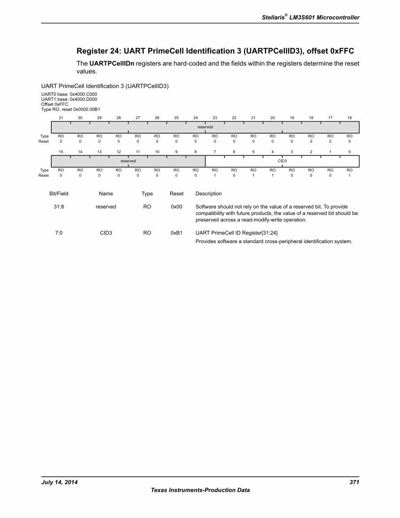
Register 24: UART PrimeCell Identification 3 (UARTPCellID3), offset 0xFFCThe UARTPCellIDn registers are hard-coded and the fields within the registers determine the resetvalues.
UART PrimeCell Identification 3 (UARTPCellID3)UART0 base: 0x4000.C000UART1 base: 0x4000.D000Offset 0xFFCType RO, reset 0x0000.00B1
16171819202122232425262728293031
reserved
ROROROROROROROROROROROROROROROROType0000000000000000Reset
0123456789101112131415
CID3reserved
ROROROROROROROROROROROROROROROROType1000110100000000Reset
DescriptionResetTypeNameBit/Field
Software should not rely on the value of a reserved bit. To providecompatibility with future products, the value of a reserved bit should bepreserved across a read-modify-write operation.
0x00ROreserved31:8
UART PrimeCell ID Register[31:24]Provides software a standard cross-peripheral identification system.
0xB1ROCID37:0
371July 14, 2014Texas Instruments-Production Data
Stellaris® LM3S601 Microcontroller
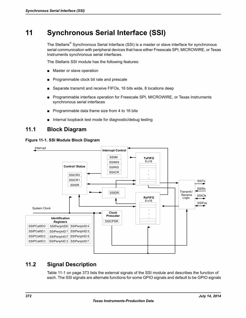
11 Synchronous Serial Interface (SSI)The Stellaris® Synchronous Serial Interface (SSI) is a master or slave interface for synchronousserial communication with peripheral devices that have either Freescale SPI, MICROWIRE, or TexasInstruments synchronous serial interfaces.
The Stellaris SSI module has the following features:
Master or slave operation
Programmable clock bit rate and prescale
Separate transmit and receive FIFOs, 16 bits wide, 8 locations deep
Programmable interface operation for Freescale SPI, MICROWIRE, or Texas Instrumentssynchronous serial interfaces
Programmable data frame size from 4 to 16 bits
Internal loopback test mode for diagnostic/debug testing
11.1 Block Diagram
Figure 11-1. SSI Module Block Diagram
Transmit /ReceiveLogic
ClockPrescaler
SSICPSR
SSICR0
SSICR1
SSISR
Interrupt Control
SSIIM
SSIMIS
SSIRIS
SSIICR
SSIDR
TxFIFO8 x16
.
.
.
RxFIFO8 x16
.
.
.
System Clock
SSITx
SSIRx
SSIClk
SSIFss
Interrupt
IdentificationRegisters
SSIPCellID0 0 SSIPeriphID4
SSIPCellID1 1 SSIPeriphID 5
SSIPCellID2 2 SSIPeriphID 6
SSIPCellID3 SSIPeriphID 3 SSIPeriphID7
Control/ Status
SSIPeriphID
SSIPeriphID
SSIPeriphID
11.2 Signal DescriptionTable 11-1 on page 373 lists the external signals of the SSI module and describes the function ofeach. The SSI signals are alternate functions for some GPIO signals and default to be GPIO signals
July 14, 2014372Texas Instruments-Production Data
Synchronous Serial Interface (SSI)
at reset., with the exception of the SSI0Clk, SSI0Fss, SSI0Rx, and SSI0Tx pins which defaultto the SSI function. The column in the table below titled "Pin Assignment" lists the possible GPIOpin placements for the SSI signals. The AFSEL bit in the GPIO Alternate Function Select(GPIOAFSEL) register (page 250) should be set to choose the SSI function. For more informationon configuring GPIOs, see “General-Purpose Input/Outputs (GPIOs)” on page 230.
Table 11-1. SSI Signals (48QFP)
DescriptionBuffer TypeaPin TypePin NumberPin Name
SSI clock.TTLI/O19SSIClk
SSI frame.TTLI/O20SSIFss
SSI receive.TTLI21SSIRx
SSI transmit.TTLO22SSITx
a. The TTL designation indicates the pin has TTL-compatible voltage levels.
11.3 Functional DescriptionThe SSI performs serial-to-parallel conversion on data received from a peripheral device. The CPUaccesses data, control, and status information. The transmit and receive paths are buffered withinternal FIFOmemories allowing up to eight 16-bit values to be stored independently in both transmitand receive modes.
11.3.1 Bit Rate GenerationThe SSI includes a programmable bit rate clock divider and prescaler to generate the serial outputclock. Bit rates are supported to 1.5 MHz and higher, although maximum bit rate is determined byperipheral devices.
The serial bit rate is derived by dividing down the input clock (FSysClk). The clock is first dividedby an even prescale value CPSDVSR from 2 to 254, which is programmed in the SSI Clock Prescale(SSICPSR) register (see page 392). The clock is further divided by a value from 1 to 256, which is1 + SCR, where SCR is the value programmed in the SSI Control0 (SSICR0) register (see page 385).
The frequency of the output clock SSIClk is defined by:
SSIClk = FSysClk / (CPSDVSR * (1 + SCR))
Note: For master mode, the system clock must be at least two times faster than the SSIClk. Forslave mode, the system clock must be at least 12 times faster than the SSIClk.
See “Synchronous Serial Interface (SSI)” on page 534 to view SSI timing parameters.
11.3.2 FIFO Operation
11.3.2.1 Transmit FIFOThe common transmit FIFO is a 16-bit wide, 8-locations deep, first-in, first-out memory buffer. TheCPU writes data to the FIFO by writing the SSI Data (SSIDR) register (see page 389), and data isstored in the FIFO until it is read out by the transmission logic.
When configured as a master or a slave, parallel data is written into the transmit FIFO prior to serialconversion and transmission to the attached slave or master, respectively, through the SSITx pin.
In slave mode, the SSI transmits data each time the master initiates a transaction. If the transmitFIFO is empty and the master initiates, the slave transmits the 8th most recent value in the transmitFIFO. If less than 8 values have been written to the transmit FIFO since the SSI module clock was
373July 14, 2014Texas Instruments-Production Data
Stellaris® LM3S601 Microcontroller
enabled using the SSI bit in the RGCG1 register, then 0 is transmitted. Care should be taken toensure that valid data is in the FIFO as needed. The SSI can be configured to generate an interruptwhen the FIFO is empty.
11.3.2.2 Receive FIFOThe common receive FIFO is a 16-bit wide, 8-locations deep, first-in, first-out memory buffer.Received data from the serial interface is stored in the buffer until read out by the CPU, whichaccesses the read FIFO by reading the SSIDR register.
When configured as a master or slave, serial data received through the SSIRx pin is registeredprior to parallel loading into the attached slave or master receive FIFO, respectively.
11.3.3 InterruptsThe SSI can generate interrupts when the following conditions are observed:
Transmit FIFO service
Receive FIFO service
Receive FIFO time-out
Receive FIFO overrun
All of the interrupt events are ORed together before being sent to the interrupt controller, so the SSIcan only generate a single interrupt request to the controller at any given time. You can mask eachof the four individual maskable interrupts by setting the appropriate bits in the SSI Interrupt Mask(SSIIM) register (see page 393). Setting the appropriate mask bit to 1 enables the interrupt.
Provision of the individual outputs, as well as a combined interrupt output, allows use of either aglobal interrupt service routine, or modular device drivers to handle interrupts. The transmit andreceive dynamic dataflow interrupts have been separated from the status interrupts so that datacan be read or written in response to the FIFO trigger levels. The status of the individual interruptsources can be read from the SSI Raw Interrupt Status (SSIRIS) and SSI Masked Interrupt Status(SSIMIS) registers (see page 395 and page 396, respectively).
11.3.4 Frame FormatsEach data frame is between 4 and 16 bits long, depending on the size of data programmed, and istransmitted starting with the MSB. There are three basic frame types that can be selected:
Texas Instruments synchronous serial
Freescale SPI
MICROWIRE
For all three formats, the serial clock (SSIClk) is held inactive while the SSI is idle, and SSIClktransitions at the programmed frequency only during active transmission or reception of data. Theidle state of SSIClk is utilized to provide a receive timeout indication that occurs when the receiveFIFO still contains data after a timeout period.
For Freescale SPI and MICROWIRE frame formats, the serial frame (SSIFss ) pin is active Low,and is asserted (pulled down) during the entire transmission of the frame.
July 14, 2014374Texas Instruments-Production Data
Synchronous Serial Interface (SSI)
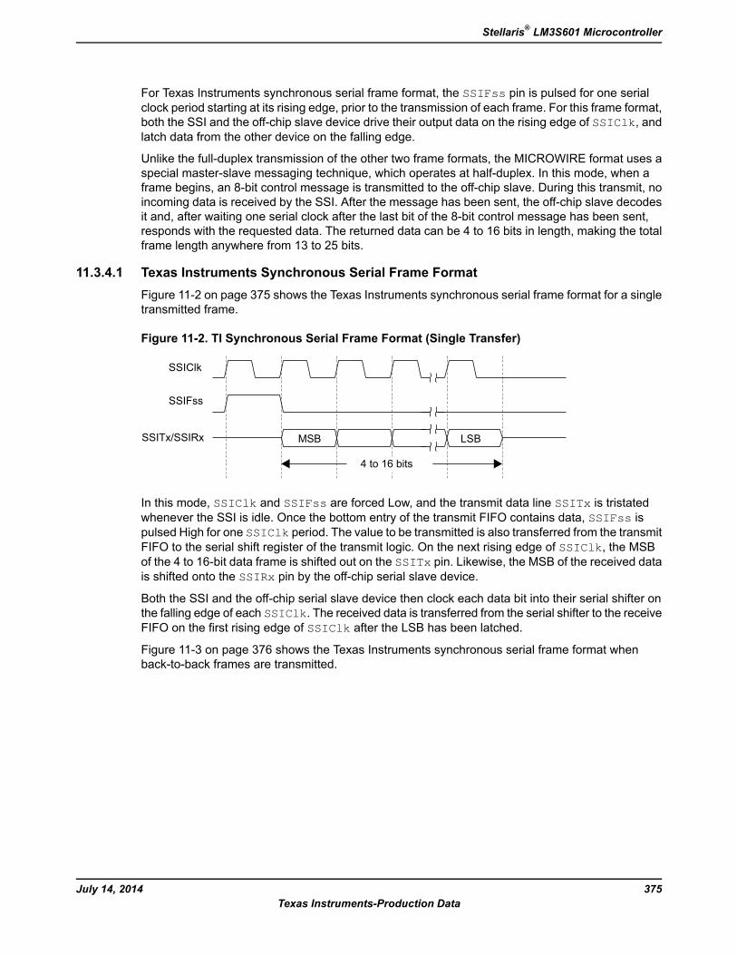
For Texas Instruments synchronous serial frame format, the SSIFss pin is pulsed for one serialclock period starting at its rising edge, prior to the transmission of each frame. For this frame format,both the SSI and the off-chip slave device drive their output data on the rising edge of SSIClk, andlatch data from the other device on the falling edge.
Unlike the full-duplex transmission of the other two frame formats, the MICROWIRE format uses aspecial master-slave messaging technique, which operates at half-duplex. In this mode, when aframe begins, an 8-bit control message is transmitted to the off-chip slave. During this transmit, noincoming data is received by the SSI. After the message has been sent, the off-chip slave decodesit and, after waiting one serial clock after the last bit of the 8-bit control message has been sent,responds with the requested data. The returned data can be 4 to 16 bits in length, making the totalframe length anywhere from 13 to 25 bits.
11.3.4.1 Texas Instruments Synchronous Serial Frame FormatFigure 11-2 on page 375 shows the Texas Instruments synchronous serial frame format for a singletransmitted frame.
Figure 11-2. TI Synchronous Serial Frame Format (Single Transfer)
SSIClk
SSIFss
SSITx/SSIRx MSB LSB
4 to 16 bits
In this mode, SSIClk and SSIFss are forced Low, and the transmit data line SSITx is tristatedwhenever the SSI is idle. Once the bottom entry of the transmit FIFO contains data, SSIFss ispulsed High for one SSIClk period. The value to be transmitted is also transferred from the transmitFIFO to the serial shift register of the transmit logic. On the next rising edge of SSIClk, the MSBof the 4 to 16-bit data frame is shifted out on the SSITx pin. Likewise, the MSB of the received datais shifted onto the SSIRx pin by the off-chip serial slave device.
Both the SSI and the off-chip serial slave device then clock each data bit into their serial shifter onthe falling edge of each SSIClk. The received data is transferred from the serial shifter to the receiveFIFO on the first rising edge of SSIClk after the LSB has been latched.
Figure 11-3 on page 376 shows the Texas Instruments synchronous serial frame format whenback-to-back frames are transmitted.
375July 14, 2014Texas Instruments-Production Data
Stellaris® LM3S601 Microcontroller
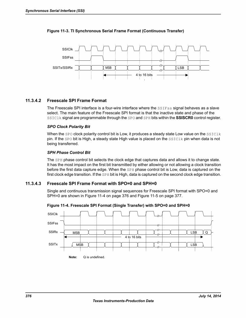
Figure 11-3. TI Synchronous Serial Frame Format (Continuous Transfer)
MSB LSB
SSIClk
SSIFss
SSITx/SSIRx
4 to 16 bits
11.3.4.2 Freescale SPI Frame FormatThe Freescale SPI interface is a four-wire interface where the SSIFss signal behaves as a slaveselect. The main feature of the Freescale SPI format is that the inactive state and phase of theSSIClk signal are programmable through the SPO and SPH bits within the SSISCR0 control register.
SPO Clock Polarity Bit
When the SPO clock polarity control bit is Low, it produces a steady state Low value on the SSIClkpin. If the SPO bit is High, a steady state High value is placed on the SSIClk pin when data is notbeing transferred.
SPH Phase Control Bit
The SPH phase control bit selects the clock edge that captures data and allows it to change state.It has the most impact on the first bit transmitted by either allowing or not allowing a clock transitionbefore the first data capture edge. When the SPH phase control bit is Low, data is captured on thefirst clock edge transition. If the SPH bit is High, data is captured on the second clock edge transition.
11.3.4.3 Freescale SPI Frame Format with SPO=0 and SPH=0Single and continuous transmission signal sequences for Freescale SPI format with SPO=0 andSPH=0 are shown in Figure 11-4 on page 376 and Figure 11-5 on page 377.
Figure 11-4. Freescale SPI Format (Single Transfer) with SPO=0 and SPH=0
SSIClk
SSIFss
SSIRx Q
SSITx MSB
MSB
LSB
LSB4 to 16 bits
Note: Q is undefined.
July 14, 2014376Texas Instruments-Production Data
Synchronous Serial Interface (SSI)
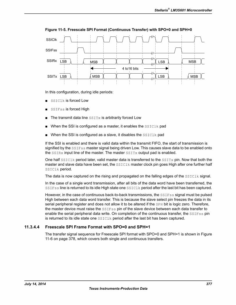
Figure 11-5. Freescale SPI Format (Continuous Transfer) with SPO=0 and SPH=0
SSIClk
SSIFss
SSIRx LSB
SSITx MSB LSB
LSB MSB
MSB
MSB
LSB
4 to16 bits
In this configuration, during idle periods:
SSIClk is forced Low
SSIFss is forced High
The transmit data line SSITx is arbitrarily forced Low
When the SSI is configured as a master, it enables the SSIClk pad
When the SSI is configured as a slave, it disables the SSIClk pad
If the SSI is enabled and there is valid data within the transmit FIFO, the start of transmission issignified by the SSIFssmaster signal being driven Low. This causes slave data to be enabled ontothe SSIRx input line of the master. The master SSITx output pad is enabled.
One half SSIClk period later, valid master data is transferred to the SSITx pin. Now that both themaster and slave data have been set, the SSIClkmaster clock pin goes High after one further halfSSIClk period.
The data is now captured on the rising and propagated on the falling edges of the SSIClk signal.
In the case of a single word transmission, after all bits of the data word have been transferred, theSSIFss line is returned to its idle High state one SSIClk period after the last bit has been captured.
However, in the case of continuous back-to-back transmissions, the SSIFss signal must be pulsedHigh between each data word transfer. This is because the slave select pin freezes the data in itsserial peripheral register and does not allow it to be altered if the SPH bit is logic zero. Therefore,the master device must raise the SSIFss pin of the slave device between each data transfer toenable the serial peripheral data write. On completion of the continuous transfer, the SSIFss pinis returned to its idle state one SSIClk period after the last bit has been captured.
11.3.4.4 Freescale SPI Frame Format with SPO=0 and SPH=1The transfer signal sequence for Freescale SPI format with SPO=0 and SPH=1 is shown in Figure11-6 on page 378, which covers both single and continuous transfers.
377July 14, 2014Texas Instruments-Production Data
Stellaris® LM3S601 Microcontroller
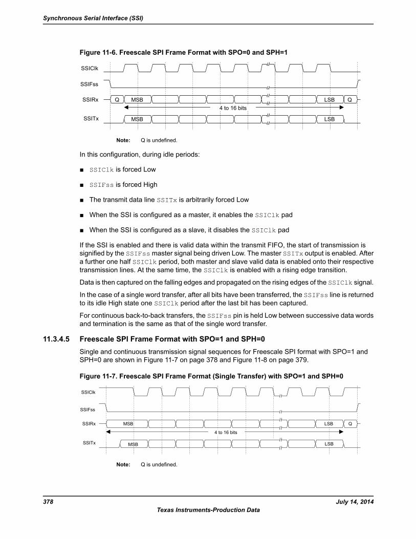
Figure 11-6. Freescale SPI Frame Format with SPO=0 and SPH=1
SSIClk
SSIFss
SSIRx
SSITx
Q
MSB
QMSB
LSB
LSB4 to 16 bits
Q
Note: Q is undefined.
In this configuration, during idle periods:
SSIClk is forced Low
SSIFss is forced High
The transmit data line SSITx is arbitrarily forced Low
When the SSI is configured as a master, it enables the SSIClk pad
When the SSI is configured as a slave, it disables the SSIClk pad
If the SSI is enabled and there is valid data within the transmit FIFO, the start of transmission issignified by the SSIFssmaster signal being driven Low. The master SSITx output is enabled. Aftera further one half SSIClk period, both master and slave valid data is enabled onto their respectivetransmission lines. At the same time, the SSIClk is enabled with a rising edge transition.
Data is then captured on the falling edges and propagated on the rising edges of the SSIClk signal.
In the case of a single word transfer, after all bits have been transferred, the SSIFss line is returnedto its idle High state one SSIClk period after the last bit has been captured.
For continuous back-to-back transfers, the SSIFss pin is held Low between successive data wordsand termination is the same as that of the single word transfer.
11.3.4.5 Freescale SPI Frame Format with SPO=1 and SPH=0Single and continuous transmission signal sequences for Freescale SPI format with SPO=1 andSPH=0 are shown in Figure 11-7 on page 378 and Figure 11-8 on page 379.
Figure 11-7. Freescale SPI Frame Format (Single Transfer) with SPO=1 and SPH=0
SSIClk
SSIFss
SSIRx
SSITx
QMSB
MSB LSB
LSB
4 to 16 bits
Note: Q is undefined.
July 14, 2014378Texas Instruments-Production Data
Synchronous Serial Interface (SSI)
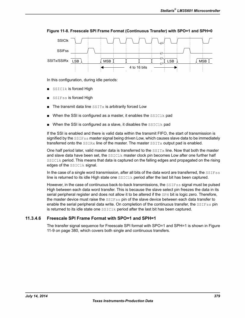
Figure 11-8. Freescale SPI Frame Format (Continuous Transfer) with SPO=1 and SPH=0
SSIClk
SSIFss
SSITx/SSIRx MSB LSBLSB MSB
4 to 16 bits
In this configuration, during idle periods:
SSIClk is forced High
SSIFss is forced High
The transmit data line SSITx is arbitrarily forced Low
When the SSI is configured as a master, it enables the SSIClk pad
When the SSI is configured as a slave, it disables the SSIClk pad
If the SSI is enabled and there is valid data within the transmit FIFO, the start of transmission issignified by the SSIFssmaster signal being driven Low, which causes slave data to be immediatelytransferred onto the SSIRx line of the master. The master SSITx output pad is enabled.
One half period later, valid master data is transferred to the SSITx line. Now that both the masterand slave data have been set, the SSIClk master clock pin becomes Low after one further halfSSIClk period. This means that data is captured on the falling edges and propagated on the risingedges of the SSIClk signal.
In the case of a single word transmission, after all bits of the data word are transferred, the SSIFssline is returned to its idle High state one SSIClk period after the last bit has been captured.
However, in the case of continuous back-to-back transmissions, the SSIFss signal must be pulsedHigh between each data word transfer. This is because the slave select pin freezes the data in itsserial peripheral register and does not allow it to be altered if the SPH bit is logic zero. Therefore,the master device must raise the SSIFss pin of the slave device between each data transfer toenable the serial peripheral data write. On completion of the continuous transfer, the SSIFss pinis returned to its idle state one SSIClk period after the last bit has been captured.
11.3.4.6 Freescale SPI Frame Format with SPO=1 and SPH=1The transfer signal sequence for Freescale SPI format with SPO=1 and SPH=1 is shown in Figure11-9 on page 380, which covers both single and continuous transfers.
379July 14, 2014Texas Instruments-Production Data
Stellaris® LM3S601 Microcontroller
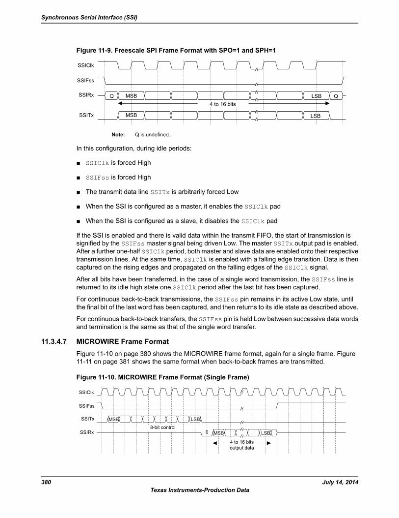
Figure 11-9. Freescale SPI Frame Format with SPO=1 and SPH=1
SSIClk
SSIFss
SSIRx
SSITx
Q
MSB
MSB
LSB
LSB4 to 16 bits
Q
Note: Q is undefined.
In this configuration, during idle periods:
SSIClk is forced High
SSIFss is forced High
The transmit data line SSITx is arbitrarily forced Low
When the SSI is configured as a master, it enables the SSIClk pad
When the SSI is configured as a slave, it disables the SSIClk pad
If the SSI is enabled and there is valid data within the transmit FIFO, the start of transmission issignified by the SSIFss master signal being driven Low. The master SSITx output pad is enabled.After a further one-half SSIClk period, both master and slave data are enabled onto their respectivetransmission lines. At the same time, SSIClk is enabled with a falling edge transition. Data is thencaptured on the rising edges and propagated on the falling edges of the SSIClk signal.
After all bits have been transferred, in the case of a single word transmission, the SSIFss line isreturned to its idle high state one SSIClk period after the last bit has been captured.
For continuous back-to-back transmissions, the SSIFss pin remains in its active Low state, untilthe final bit of the last word has been captured, and then returns to its idle state as described above.
For continuous back-to-back transfers, the SSIFss pin is held Low between successive data wordsand termination is the same as that of the single word transfer.
11.3.4.7 MICROWIRE Frame FormatFigure 11-10 on page 380 shows the MICROWIRE frame format, again for a single frame. Figure11-11 on page 381 shows the same format when back-to-back frames are transmitted.
Figure 11-10. MICROWIRE Frame Format (Single Frame)
SSIClk
SSIFss
SSIRx 0
SSITx
8-bit control
4 to 16 bitsoutput data
LSB
MSB
MSB
LSB
July 14, 2014380Texas Instruments-Production Data
Synchronous Serial Interface (SSI)
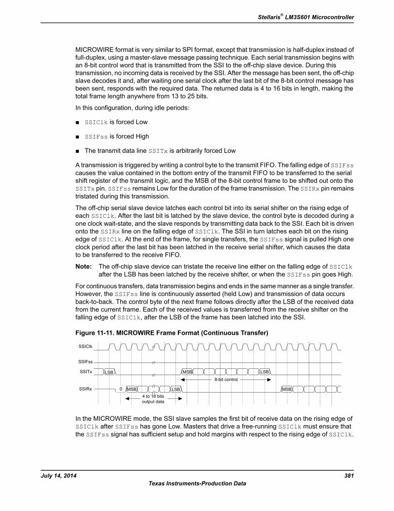
MICROWIRE format is very similar to SPI format, except that transmission is half-duplex instead offull-duplex, using a master-slave message passing technique. Each serial transmission begins withan 8-bit control word that is transmitted from the SSI to the off-chip slave device. During thistransmission, no incoming data is received by the SSI. After the message has been sent, the off-chipslave decodes it and, after waiting one serial clock after the last bit of the 8-bit control message hasbeen sent, responds with the required data. The returned data is 4 to 16 bits in length, making thetotal frame length anywhere from 13 to 25 bits.
In this configuration, during idle periods:
SSIClk is forced Low
SSIFss is forced High
The transmit data line SSITx is arbitrarily forced Low
A transmission is triggered by writing a control byte to the transmit FIFO. The falling edge of SSIFsscauses the value contained in the bottom entry of the transmit FIFO to be transferred to the serialshift register of the transmit logic, and the MSB of the 8-bit control frame to be shifted out onto theSSITx pin. SSIFss remains Low for the duration of the frame transmission. The SSIRx pin remainstristated during this transmission.
The off-chip serial slave device latches each control bit into its serial shifter on the rising edge ofeach SSIClk. After the last bit is latched by the slave device, the control byte is decoded during aone clock wait-state, and the slave responds by transmitting data back to the SSI. Each bit is drivenonto the SSIRx line on the falling edge of SSIClk. The SSI in turn latches each bit on the risingedge of SSIClk. At the end of the frame, for single transfers, the SSIFss signal is pulled High oneclock period after the last bit has been latched in the receive serial shifter, which causes the datato be transferred to the receive FIFO.
Note: The off-chip slave device can tristate the receive line either on the falling edge of SSIClkafter the LSB has been latched by the receive shifter, or when the SSIFss pin goes High.
For continuous transfers, data transmission begins and ends in the samemanner as a single transfer.However, the SSIFss line is continuously asserted (held Low) and transmission of data occursback-to-back. The control byte of the next frame follows directly after the LSB of the received datafrom the current frame. Each of the received values is transferred from the receive shifter on thefalling edge of SSIClk, after the LSB of the frame has been latched into the SSI.
Figure 11-11. MICROWIRE Frame Format (Continuous Transfer)
SSIClk
SSIFss
LSBMSBSSIRx 0
SSITx LSBLSB
MSB4 to 16 bitsoutput data
8-bit control
MSB
In the MICROWIRE mode, the SSI slave samples the first bit of receive data on the rising edge ofSSIClk after SSIFss has gone Low. Masters that drive a free-running SSIClk must ensure thatthe SSIFss signal has sufficient setup and hold margins with respect to the rising edge of SSIClk.
381July 14, 2014Texas Instruments-Production Data
Stellaris® LM3S601 Microcontroller
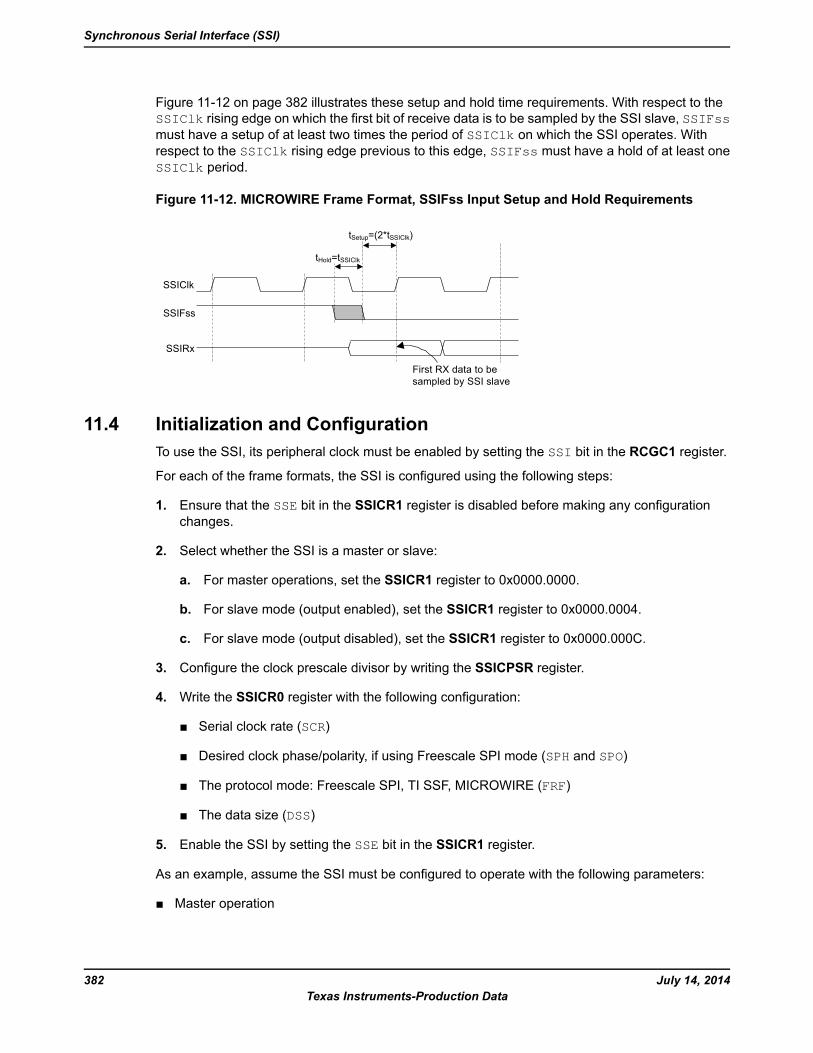
Figure 11-12 on page 382 illustrates these setup and hold time requirements. With respect to theSSIClk rising edge on which the first bit of receive data is to be sampled by the SSI slave, SSIFssmust have a setup of at least two times the period of SSIClk on which the SSI operates. Withrespect to the SSIClk rising edge previous to this edge, SSIFss must have a hold of at least oneSSIClk period.
Figure 11-12. MICROWIRE Frame Format, SSIFss Input Setup and Hold Requirements
SSIClk
SSIFss
SSIRx
First RX data to besampled by SSI slave
tHold=tSSIClk
tSetup=(2*tSSIClk)
11.4 Initialization and ConfigurationTo use the SSI, its peripheral clock must be enabled by setting the SSI bit in the RCGC1 register.
For each of the frame formats, the SSI is configured using the following steps:
1. Ensure that the SSE bit in the SSICR1 register is disabled before making any configurationchanges.
2. Select whether the SSI is a master or slave:
a. For master operations, set the SSICR1 register to 0x0000.0000.
b. For slave mode (output enabled), set the SSICR1 register to 0x0000.0004.
c. For slave mode (output disabled), set the SSICR1 register to 0x0000.000C.
3. Configure the clock prescale divisor by writing the SSICPSR register.
4. Write the SSICR0 register with the following configuration:
Serial clock rate (SCR)
Desired clock phase/polarity, if using Freescale SPI mode (SPH and SPO)
The protocol mode: Freescale SPI, TI SSF, MICROWIRE (FRF)
The data size (DSS)
5. Enable the SSI by setting the SSE bit in the SSICR1 register.
As an example, assume the SSI must be configured to operate with the following parameters:
Master operation
July 14, 2014382Texas Instruments-Production Data
Synchronous Serial Interface (SSI)
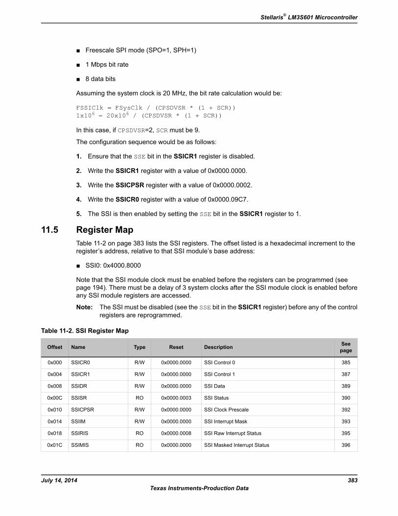
Freescale SPI mode (SPO=1, SPH=1)
1 Mbps bit rate
8 data bits
Assuming the system clock is 20 MHz, the bit rate calculation would be:
FSSIClk = FSysClk / (CPSDVSR * (1 + SCR))1x106 = 20x106 / (CPSDVSR * (1 + SCR))
In this case, if CPSDVSR=2, SCR must be 9.
The configuration sequence would be as follows:
1. Ensure that the SSE bit in the SSICR1 register is disabled.
2. Write the SSICR1 register with a value of 0x0000.0000.
3. Write the SSICPSR register with a value of 0x0000.0002.
4. Write the SSICR0 register with a value of 0x0000.09C7.
5. The SSI is then enabled by setting the SSE bit in the SSICR1 register to 1.
11.5 Register MapTable 11-2 on page 383 lists the SSI registers. The offset listed is a hexadecimal increment to theregister’s address, relative to that SSI module’s base address:
SSI0: 0x4000.8000
Note that the SSI module clock must be enabled before the registers can be programmed (seepage 194). There must be a delay of 3 system clocks after the SSI module clock is enabled beforeany SSI module registers are accessed.
Note: The SSI must be disabled (see the SSE bit in the SSICR1 register) before any of the controlregisters are reprogrammed.
Table 11-2. SSI Register Map
SeepageDescriptionResetTypeNameOffset
385SSI Control 00x0000.0000R/WSSICR00x000
387SSI Control 10x0000.0000R/WSSICR10x004
389SSI Data0x0000.0000R/WSSIDR0x008
390SSI Status0x0000.0003ROSSISR0x00C
392SSI Clock Prescale0x0000.0000R/WSSICPSR0x010
393SSI Interrupt Mask0x0000.0000R/WSSIIM0x014
395SSI Raw Interrupt Status0x0000.0008ROSSIRIS0x018
396SSI Masked Interrupt Status0x0000.0000ROSSIMIS0x01C
383July 14, 2014Texas Instruments-Production Data
Stellaris® LM3S601 Microcontroller
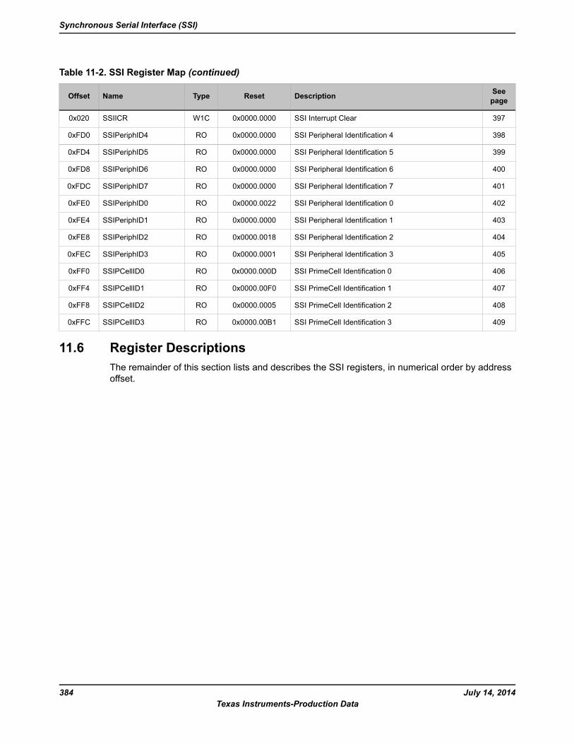
Table 11-2. SSI Register Map (continued)
SeepageDescriptionResetTypeNameOffset
397SSI Interrupt Clear0x0000.0000W1CSSIICR0x020
398SSI Peripheral Identification 40x0000.0000ROSSIPeriphID40xFD0
399SSI Peripheral Identification 50x0000.0000ROSSIPeriphID50xFD4
400SSI Peripheral Identification 60x0000.0000ROSSIPeriphID60xFD8
401SSI Peripheral Identification 70x0000.0000ROSSIPeriphID70xFDC
402SSI Peripheral Identification 00x0000.0022ROSSIPeriphID00xFE0
403SSI Peripheral Identification 10x0000.0000ROSSIPeriphID10xFE4
404SSI Peripheral Identification 20x0000.0018ROSSIPeriphID20xFE8
405SSI Peripheral Identification 30x0000.0001ROSSIPeriphID30xFEC
406SSI PrimeCell Identification 00x0000.000DROSSIPCellID00xFF0
407SSI PrimeCell Identification 10x0000.00F0ROSSIPCellID10xFF4
408SSI PrimeCell Identification 20x0000.0005ROSSIPCellID20xFF8
409SSI PrimeCell Identification 30x0000.00B1ROSSIPCellID30xFFC
11.6 Register DescriptionsThe remainder of this section lists and describes the SSI registers, in numerical order by addressoffset.
July 14, 2014384Texas Instruments-Production Data
Synchronous Serial Interface (SSI)
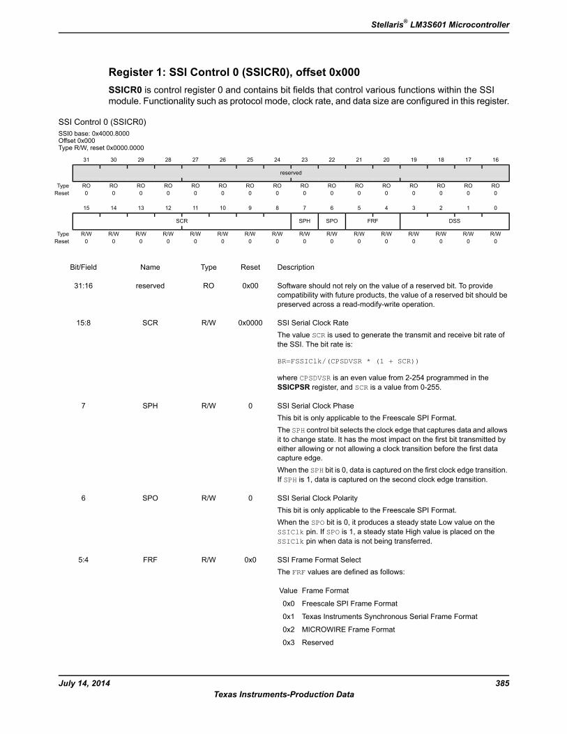
Register 1: SSI Control 0 (SSICR0), offset 0x000SSICR0 is control register 0 and contains bit fields that control various functions within the SSImodule. Functionality such as protocol mode, clock rate, and data size are configured in this register.
SSI Control 0 (SSICR0)SSI0 base: 0x4000.8000Offset 0x000Type R/W, reset 0x0000.0000
16171819202122232425262728293031
reserved
ROROROROROROROROROROROROROROROROType0000000000000000Reset
0123456789101112131415
DSSFRFSPOSPHSCR
R/WR/WR/WR/WR/WR/WR/WR/WR/WR/WR/WR/WR/WR/WR/WR/WType0000000000000000Reset
DescriptionResetTypeNameBit/Field
Software should not rely on the value of a reserved bit. To providecompatibility with future products, the value of a reserved bit should bepreserved across a read-modify-write operation.
0x00ROreserved31:16
SSI Serial Clock RateThe value SCR is used to generate the transmit and receive bit rate ofthe SSI. The bit rate is:
BR=FSSIClk/(CPSDVSR * (1 + SCR))
where CPSDVSR is an even value from 2-254 programmed in theSSICPSR register, and SCR is a value from 0-255.
0x0000R/WSCR15:8
SSI Serial Clock PhaseThis bit is only applicable to the Freescale SPI Format.The SPH control bit selects the clock edge that captures data and allowsit to change state. It has the most impact on the first bit transmitted byeither allowing or not allowing a clock transition before the first datacapture edge.When the SPH bit is 0, data is captured on the first clock edge transition.If SPH is 1, data is captured on the second clock edge transition.
0R/WSPH7
SSI Serial Clock PolarityThis bit is only applicable to the Freescale SPI Format.When the SPO bit is 0, it produces a steady state Low value on theSSIClk pin. If SPO is 1, a steady state High value is placed on theSSIClk pin when data is not being transferred.
0R/WSPO6
SSI Frame Format SelectThe FRF values are defined as follows:
Frame FormatValue
Freescale SPI Frame Format0x0
Texas Instruments Synchronous Serial Frame Format0x1
MICROWIRE Frame Format0x2
Reserved0x3
0x0R/WFRF5:4
385July 14, 2014Texas Instruments-Production Data
Stellaris® LM3S601 Microcontroller
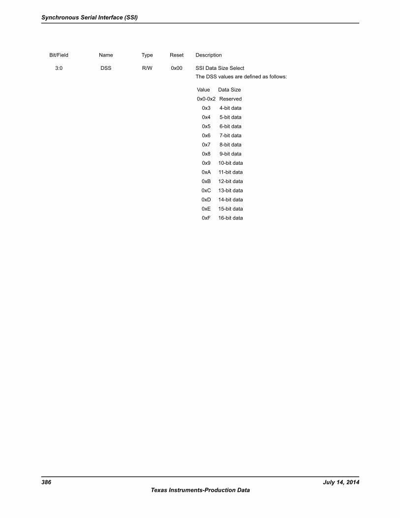
DescriptionResetTypeNameBit/Field
SSI Data Size SelectThe DSS values are defined as follows:
Data SizeValue
Reserved0x0-0x2
4-bit data0x3
5-bit data0x4
6-bit data0x5
7-bit data0x6
8-bit data0x7
9-bit data0x8
10-bit data0x9
11-bit data0xA
12-bit data0xB
13-bit data0xC
14-bit data0xD
15-bit data0xE
16-bit data0xF
0x00R/WDSS3:0
July 14, 2014386Texas Instruments-Production Data
Synchronous Serial Interface (SSI)
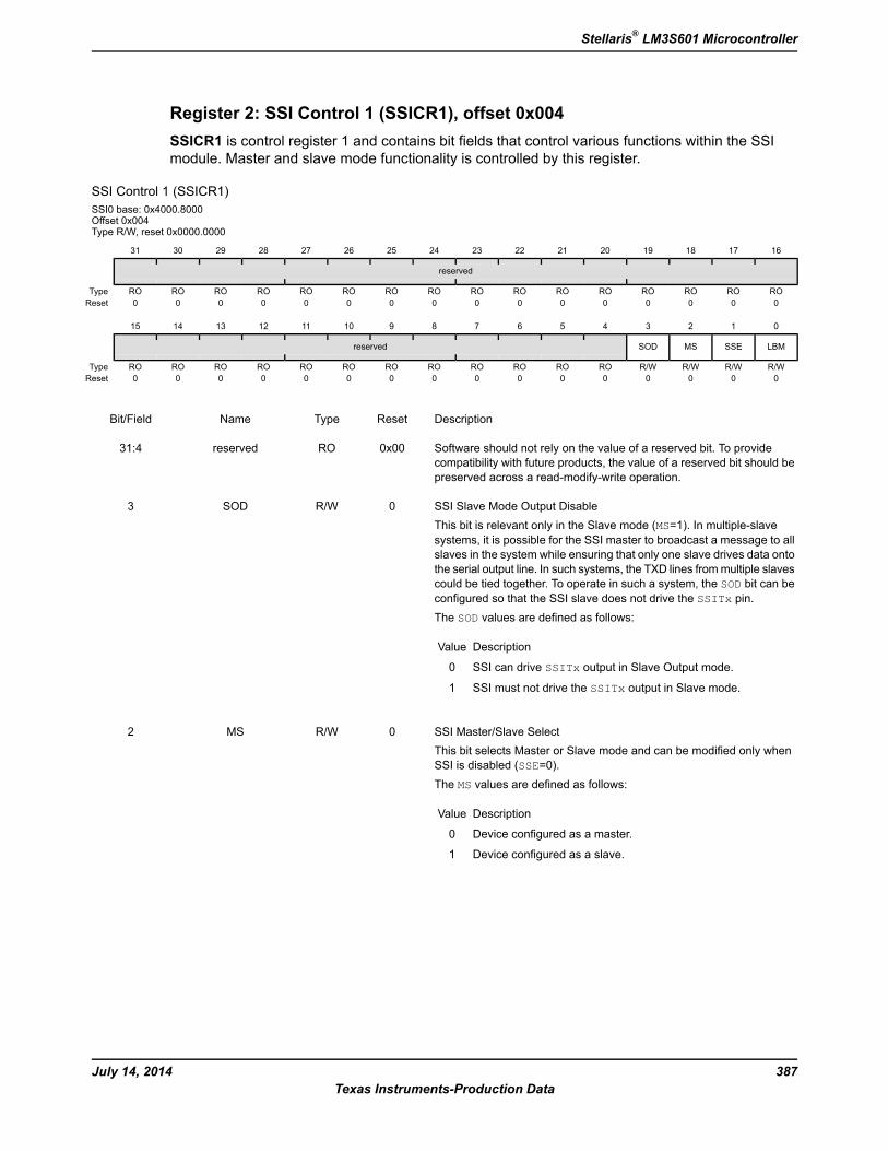
Register 2: SSI Control 1 (SSICR1), offset 0x004SSICR1 is control register 1 and contains bit fields that control various functions within the SSImodule. Master and slave mode functionality is controlled by this register.
SSI Control 1 (SSICR1)SSI0 base: 0x4000.8000Offset 0x004Type R/W, reset 0x0000.0000
16171819202122232425262728293031
reserved
ROROROROROROROROROROROROROROROROType0000000000000000Reset
0123456789101112131415
LBMSSEMSSODreserved
R/WR/WR/WR/WROROROROROROROROROROROROType0000000000000000Reset
DescriptionResetTypeNameBit/Field
Software should not rely on the value of a reserved bit. To providecompatibility with future products, the value of a reserved bit should bepreserved across a read-modify-write operation.
0x00ROreserved31:4
SSI Slave Mode Output DisableThis bit is relevant only in the Slave mode (MS=1). In multiple-slavesystems, it is possible for the SSI master to broadcast a message to allslaves in the system while ensuring that only one slave drives data ontothe serial output line. In such systems, the TXD lines frommultiple slavescould be tied together. To operate in such a system, the SOD bit can beconfigured so that the SSI slave does not drive the SSITx pin.The SOD values are defined as follows:
DescriptionValue
SSI can drive SSITx output in Slave Output mode.0
SSI must not drive the SSITx output in Slave mode.1
0R/WSOD3
SSI Master/Slave SelectThis bit selects Master or Slave mode and can be modified only whenSSI is disabled (SSE=0).The MS values are defined as follows:
DescriptionValue
Device configured as a master.0
Device configured as a slave.1
0R/WMS2
387July 14, 2014Texas Instruments-Production Data
Stellaris® LM3S601 Microcontroller
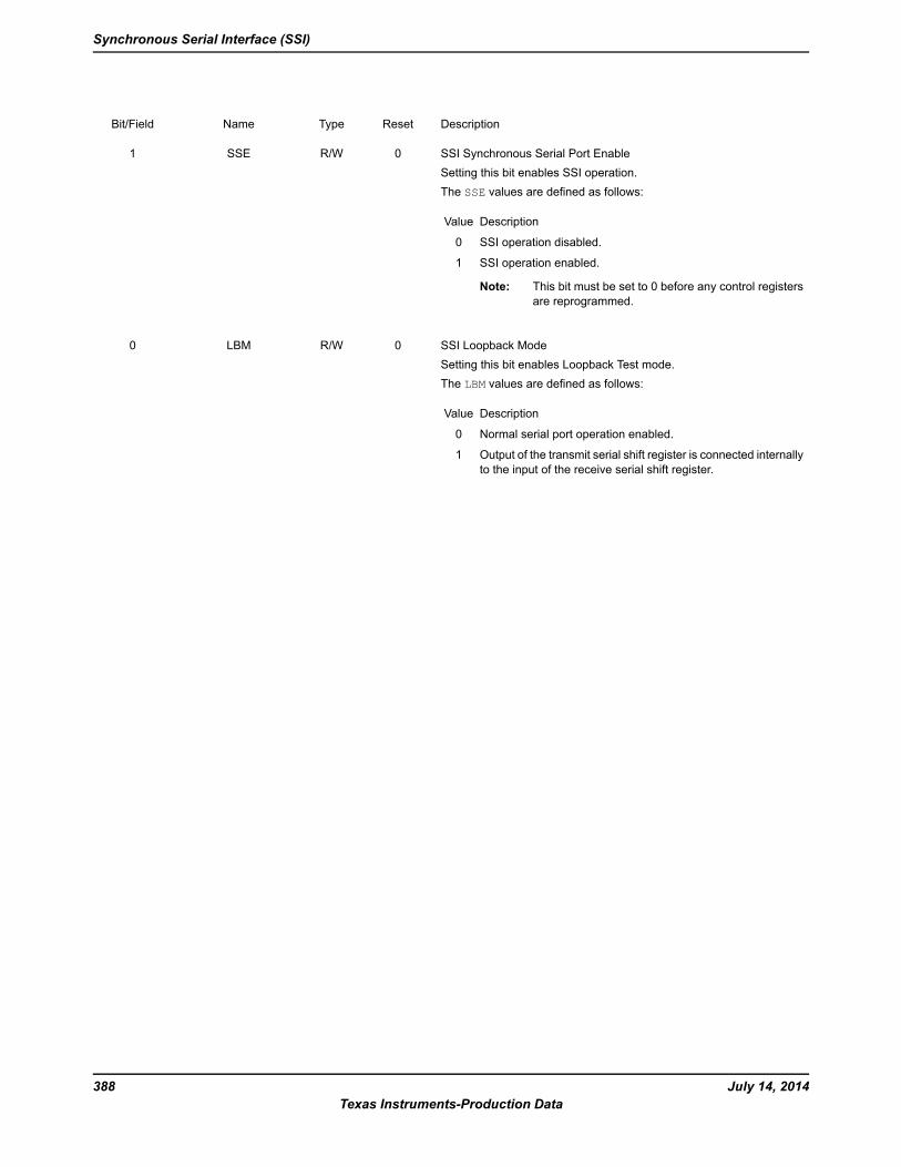
DescriptionResetTypeNameBit/Field
SSI Synchronous Serial Port EnableSetting this bit enables SSI operation.The SSE values are defined as follows:
DescriptionValue
SSI operation disabled.0
SSI operation enabled.1
Note: This bit must be set to 0 before any control registersare reprogrammed.
0R/WSSE1
SSI Loopback ModeSetting this bit enables Loopback Test mode.The LBM values are defined as follows:
DescriptionValue
Normal serial port operation enabled.0
Output of the transmit serial shift register is connected internallyto the input of the receive serial shift register.
1
0R/WLBM0
July 14, 2014388Texas Instruments-Production Data
Synchronous Serial Interface (SSI)
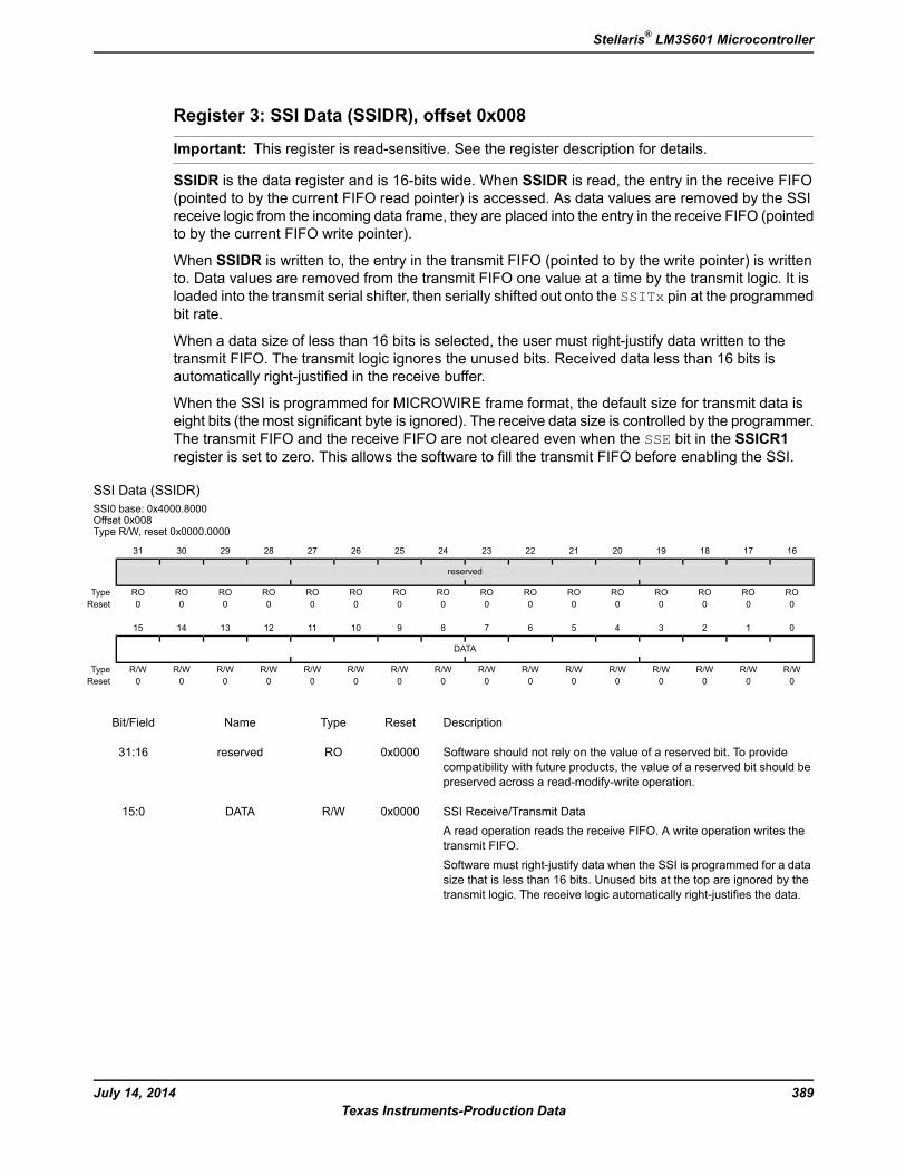
Register 3: SSI Data (SSIDR), offset 0x008
Important: This register is read-sensitive. See the register description for details.
SSIDR is the data register and is 16-bits wide. When SSIDR is read, the entry in the receive FIFO(pointed to by the current FIFO read pointer) is accessed. As data values are removed by the SSIreceive logic from the incoming data frame, they are placed into the entry in the receive FIFO (pointedto by the current FIFO write pointer).
When SSIDR is written to, the entry in the transmit FIFO (pointed to by the write pointer) is writtento. Data values are removed from the transmit FIFO one value at a time by the transmit logic. It isloaded into the transmit serial shifter, then serially shifted out onto the SSITx pin at the programmedbit rate.
When a data size of less than 16 bits is selected, the user must right-justify data written to thetransmit FIFO. The transmit logic ignores the unused bits. Received data less than 16 bits isautomatically right-justified in the receive buffer.
When the SSI is programmed for MICROWIRE frame format, the default size for transmit data iseight bits (the most significant byte is ignored). The receive data size is controlled by the programmer.The transmit FIFO and the receive FIFO are not cleared even when the SSE bit in the SSICR1register is set to zero. This allows the software to fill the transmit FIFO before enabling the SSI.
SSI Data (SSIDR)SSI0 base: 0x4000.8000Offset 0x008Type R/W, reset 0x0000.0000
16171819202122232425262728293031
reserved
ROROROROROROROROROROROROROROROROType0000000000000000Reset
0123456789101112131415
DATA
R/WR/WR/WR/WR/WR/WR/WR/WR/WR/WR/WR/WR/WR/WR/WR/WType0000000000000000Reset
DescriptionResetTypeNameBit/Field
Software should not rely on the value of a reserved bit. To providecompatibility with future products, the value of a reserved bit should bepreserved across a read-modify-write operation.
0x0000ROreserved31:16
SSI Receive/Transmit DataA read operation reads the receive FIFO. A write operation writes thetransmit FIFO.Software must right-justify data when the SSI is programmed for a datasize that is less than 16 bits. Unused bits at the top are ignored by thetransmit logic. The receive logic automatically right-justifies the data.
0x0000R/WDATA15:0
389July 14, 2014Texas Instruments-Production Data
Stellaris® LM3S601 Microcontroller
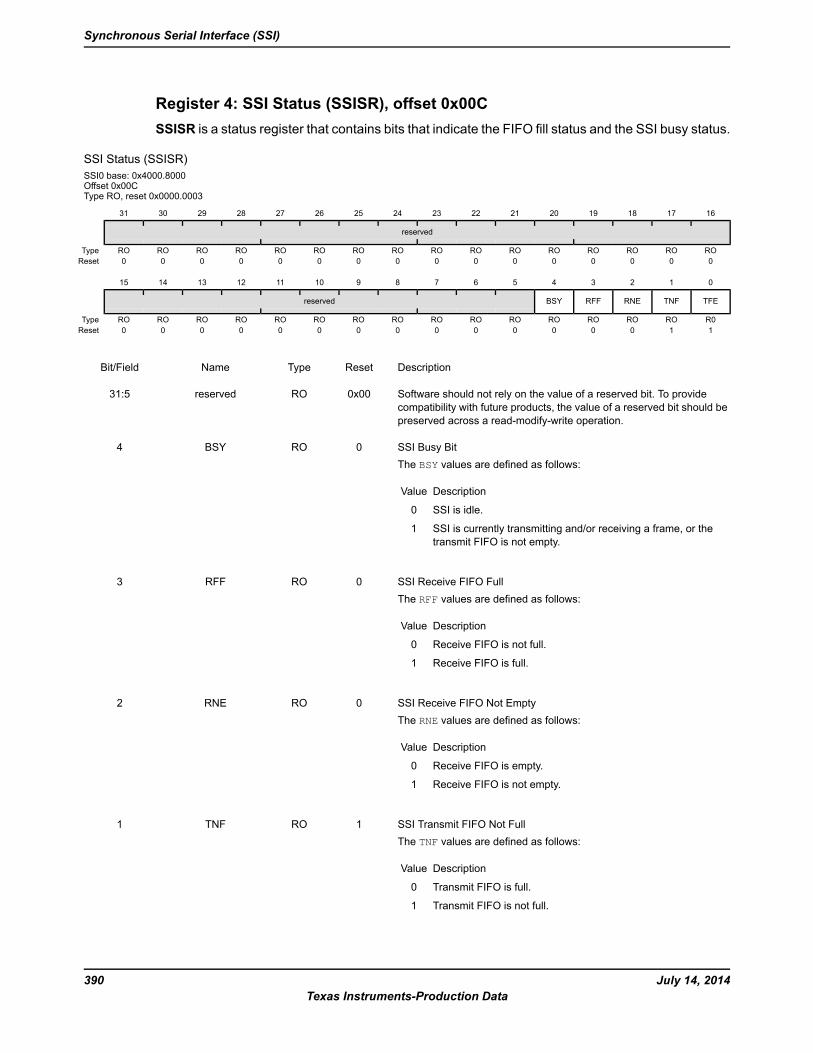
Register 4: SSI Status (SSISR), offset 0x00CSSISR is a status register that contains bits that indicate the FIFO fill status and the SSI busy status.
SSI Status (SSISR)SSI0 base: 0x4000.8000Offset 0x00CType RO, reset 0x0000.0003
16171819202122232425262728293031
reserved
ROROROROROROROROROROROROROROROROType0000000000000000Reset
0123456789101112131415
TFETNFRNERFFBSYreserved
R0ROROROROROROROROROROROROROROROType1100000000000000Reset
DescriptionResetTypeNameBit/Field
Software should not rely on the value of a reserved bit. To providecompatibility with future products, the value of a reserved bit should bepreserved across a read-modify-write operation.
0x00ROreserved31:5
SSI Busy BitThe BSY values are defined as follows:
DescriptionValue
SSI is idle.0
SSI is currently transmitting and/or receiving a frame, or thetransmit FIFO is not empty.
1
0ROBSY4
SSI Receive FIFO FullThe RFF values are defined as follows:
DescriptionValue
Receive FIFO is not full.0
Receive FIFO is full.1
0RORFF3
SSI Receive FIFO Not EmptyThe RNE values are defined as follows:
DescriptionValue
Receive FIFO is empty.0
Receive FIFO is not empty.1
0RORNE2
SSI Transmit FIFO Not FullThe TNF values are defined as follows:
DescriptionValue
Transmit FIFO is full.0
Transmit FIFO is not full.1
1ROTNF1
July 14, 2014390Texas Instruments-Production Data
Synchronous Serial Interface (SSI)
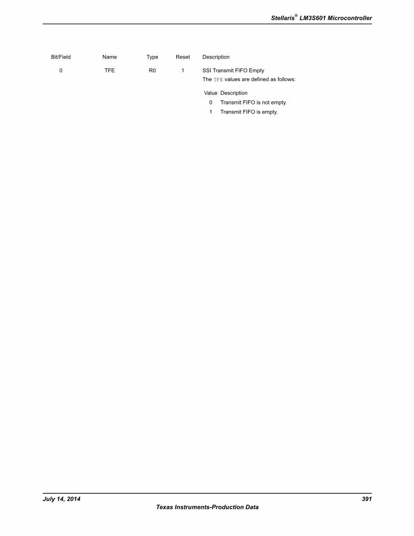
DescriptionResetTypeNameBit/Field
SSI Transmit FIFO EmptyThe TFE values are defined as follows:
DescriptionValue
Transmit FIFO is not empty.0
Transmit FIFO is empty.1
1R0TFE0
391July 14, 2014Texas Instruments-Production Data
Stellaris® LM3S601 Microcontroller
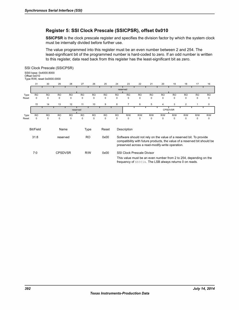
Register 5: SSI Clock Prescale (SSICPSR), offset 0x010SSICPSR is the clock prescale register and specifies the division factor by which the system clockmust be internally divided before further use.
The value programmed into this register must be an even number between 2 and 254. Theleast-significant bit of the programmed number is hard-coded to zero. If an odd number is writtento this register, data read back from this register has the least-significant bit as zero.
SSI Clock Prescale (SSICPSR)SSI0 base: 0x4000.8000Offset 0x010Type R/W, reset 0x0000.0000
16171819202122232425262728293031
reserved
ROROROROROROROROROROROROROROROROType0000000000000000Reset
0123456789101112131415
CPSDVSRreserved
R/WR/WR/WR/WR/WR/WR/WR/WROROROROROROROROType0000000000000000Reset
DescriptionResetTypeNameBit/Field
Software should not rely on the value of a reserved bit. To providecompatibility with future products, the value of a reserved bit should bepreserved across a read-modify-write operation.
0x00ROreserved31:8
SSI Clock Prescale DivisorThis value must be an even number from 2 to 254, depending on thefrequency of SSIClk. The LSB always returns 0 on reads.
0x00R/WCPSDVSR7:0
July 14, 2014392Texas Instruments-Production Data
Synchronous Serial Interface (SSI)
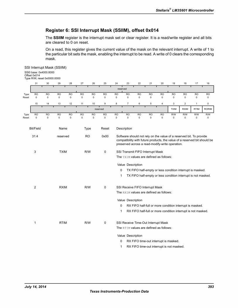
Register 6: SSI Interrupt Mask (SSIIM), offset 0x014The SSIIM register is the interrupt mask set or clear register. It is a read/write register and all bitsare cleared to 0 on reset.
On a read, this register gives the current value of the mask on the relevant interrupt. A write of 1 tothe particular bit sets the mask, enabling the interrupt to be read. A write of 0 clears the correspondingmask.
SSI Interrupt Mask (SSIIM)SSI0 base: 0x4000.8000Offset 0x014Type R/W, reset 0x0000.0000
16171819202122232425262728293031
reserved
ROROROROROROROROROROROROROROROROType0000000000000000Reset
0123456789101112131415
RORIMRTIMRXIMTXIMreserved
R/WR/WR/WR/WROROROROROROROROROROROROType0000000000000000Reset
DescriptionResetTypeNameBit/Field
Software should not rely on the value of a reserved bit. To providecompatibility with future products, the value of a reserved bit should bepreserved across a read-modify-write operation.
0x00ROreserved31:4
SSI Transmit FIFO Interrupt MaskThe TXIM values are defined as follows:
DescriptionValue
TX FIFO half-empty or less condition interrupt is masked.0
TX FIFO half-empty or less condition interrupt is not masked.1
0R/WTXIM3
SSI Receive FIFO Interrupt MaskThe RXIM values are defined as follows:
DescriptionValue
RX FIFO half-full or more condition interrupt is masked.0
RX FIFO half-full or more condition interrupt is not masked.1
0R/WRXIM2
SSI Receive Time-Out Interrupt MaskThe RTIM values are defined as follows:
DescriptionValue
RX FIFO time-out interrupt is masked.0
RX FIFO time-out interrupt is not masked.1
0R/WRTIM1
393July 14, 2014Texas Instruments-Production Data
Stellaris® LM3S601 Microcontroller
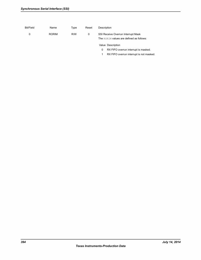
DescriptionResetTypeNameBit/Field
SSI Receive Overrun Interrupt MaskThe RORIM values are defined as follows:
DescriptionValue
RX FIFO overrun interrupt is masked.0
RX FIFO overrun interrupt is not masked.1
0R/WRORIM0
July 14, 2014394Texas Instruments-Production Data
Synchronous Serial Interface (SSI)
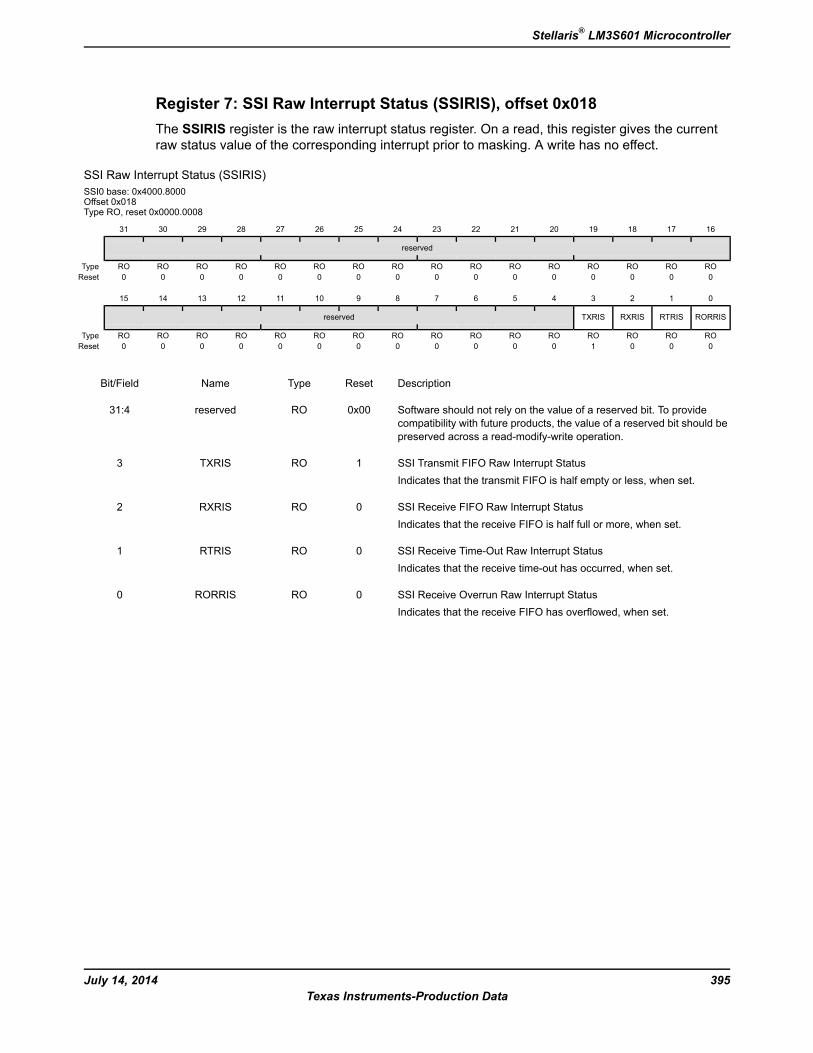
Register 7: SSI Raw Interrupt Status (SSIRIS), offset 0x018The SSIRIS register is the raw interrupt status register. On a read, this register gives the currentraw status value of the corresponding interrupt prior to masking. A write has no effect.
SSI Raw Interrupt Status (SSIRIS)SSI0 base: 0x4000.8000Offset 0x018Type RO, reset 0x0000.0008
16171819202122232425262728293031
reserved
ROROROROROROROROROROROROROROROROType0000000000000000Reset
0123456789101112131415
RORRISRTRISRXRISTXRISreserved
ROROROROROROROROROROROROROROROROType0001000000000000Reset
DescriptionResetTypeNameBit/Field
Software should not rely on the value of a reserved bit. To providecompatibility with future products, the value of a reserved bit should bepreserved across a read-modify-write operation.
0x00ROreserved31:4
SSI Transmit FIFO Raw Interrupt StatusIndicates that the transmit FIFO is half empty or less, when set.
1ROTXRIS3
SSI Receive FIFO Raw Interrupt StatusIndicates that the receive FIFO is half full or more, when set.
0RORXRIS2
SSI Receive Time-Out Raw Interrupt StatusIndicates that the receive time-out has occurred, when set.
0RORTRIS1
SSI Receive Overrun Raw Interrupt StatusIndicates that the receive FIFO has overflowed, when set.
0RORORRIS0
395July 14, 2014Texas Instruments-Production Data
Stellaris® LM3S601 Microcontroller
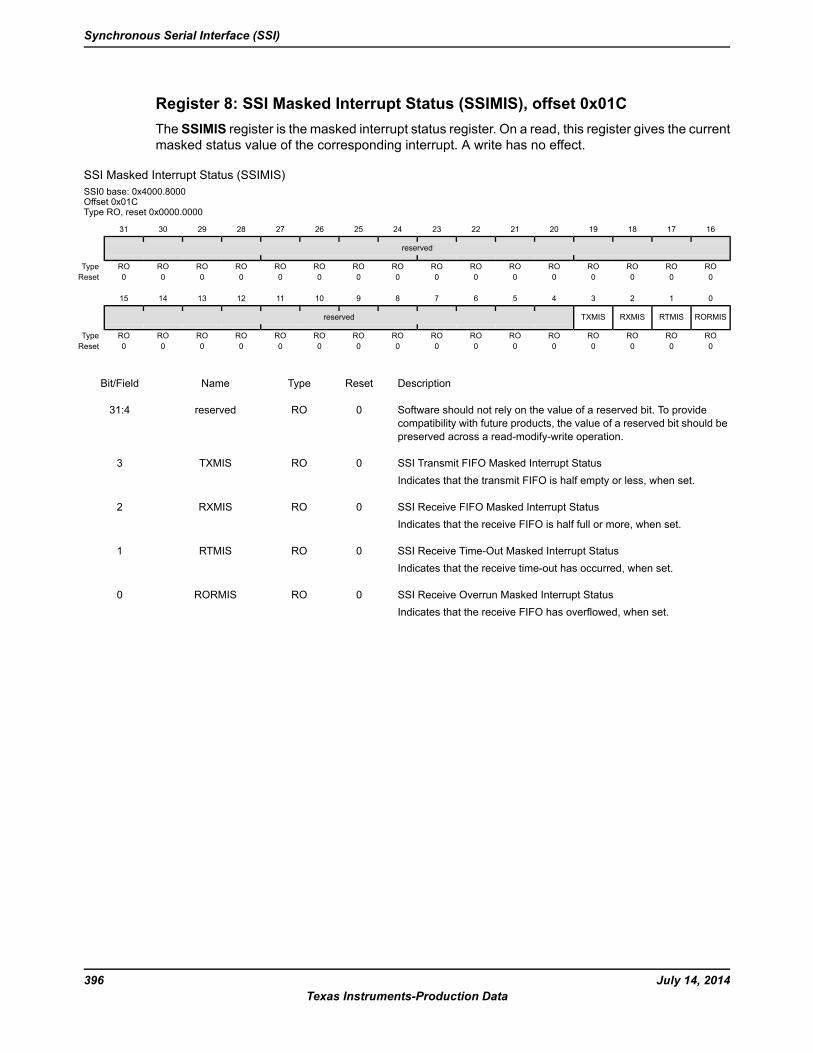
Register 8: SSI Masked Interrupt Status (SSIMIS), offset 0x01CThe SSIMIS register is the masked interrupt status register. On a read, this register gives the currentmasked status value of the corresponding interrupt. A write has no effect.
SSI Masked Interrupt Status (SSIMIS)SSI0 base: 0x4000.8000Offset 0x01CType RO, reset 0x0000.0000
16171819202122232425262728293031
reserved
ROROROROROROROROROROROROROROROROType0000000000000000Reset
0123456789101112131415
RORMISRTMISRXMISTXMISreserved
ROROROROROROROROROROROROROROROROType0000000000000000Reset
DescriptionResetTypeNameBit/Field
Software should not rely on the value of a reserved bit. To providecompatibility with future products, the value of a reserved bit should bepreserved across a read-modify-write operation.
0ROreserved31:4
SSI Transmit FIFO Masked Interrupt StatusIndicates that the transmit FIFO is half empty or less, when set.
0ROTXMIS3
SSI Receive FIFO Masked Interrupt StatusIndicates that the receive FIFO is half full or more, when set.
0RORXMIS2
SSI Receive Time-Out Masked Interrupt StatusIndicates that the receive time-out has occurred, when set.
0RORTMIS1
SSI Receive Overrun Masked Interrupt StatusIndicates that the receive FIFO has overflowed, when set.
0RORORMIS0
July 14, 2014396Texas Instruments-Production Data
Synchronous Serial Interface (SSI)
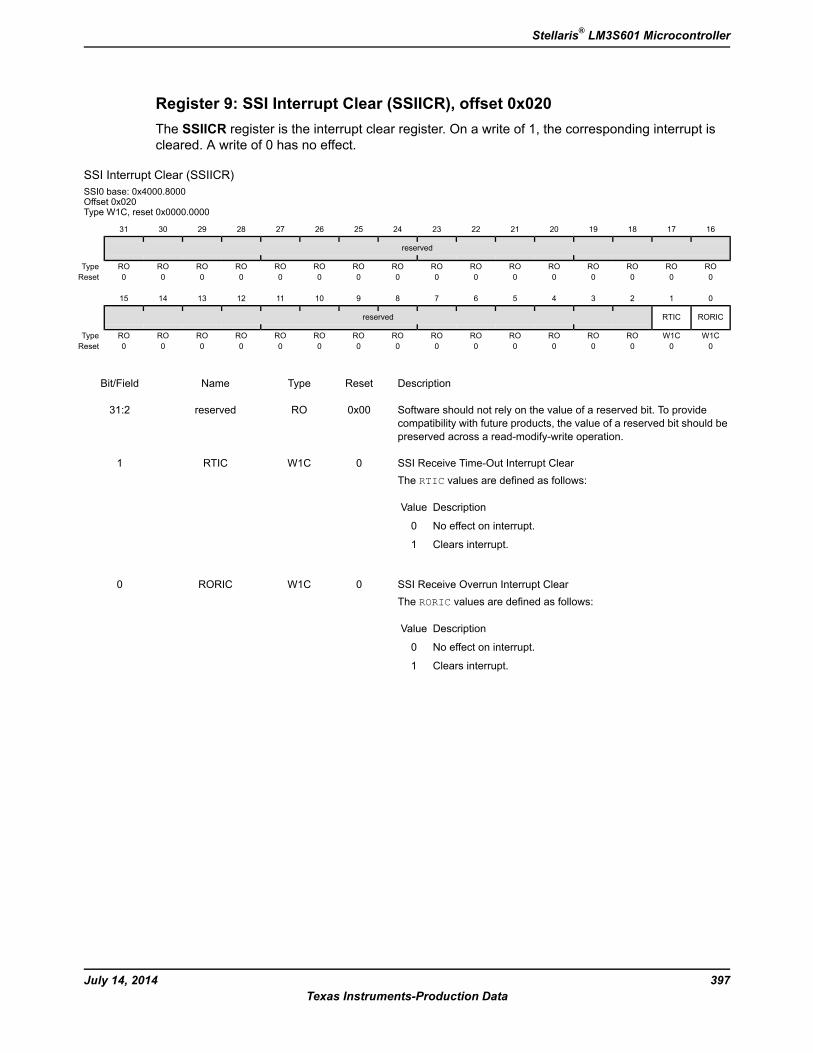
Register 9: SSI Interrupt Clear (SSIICR), offset 0x020The SSIICR register is the interrupt clear register. On a write of 1, the corresponding interrupt iscleared. A write of 0 has no effect.
SSI Interrupt Clear (SSIICR)SSI0 base: 0x4000.8000Offset 0x020Type W1C, reset 0x0000.0000
16171819202122232425262728293031
reserved
ROROROROROROROROROROROROROROROROType0000000000000000Reset
0123456789101112131415
RORICRTICreserved
W1CW1CROROROROROROROROROROROROROROType0000000000000000Reset
DescriptionResetTypeNameBit/Field
Software should not rely on the value of a reserved bit. To providecompatibility with future products, the value of a reserved bit should bepreserved across a read-modify-write operation.
0x00ROreserved31:2
SSI Receive Time-Out Interrupt ClearThe RTIC values are defined as follows:
DescriptionValue
No effect on interrupt.0
Clears interrupt.1
0W1CRTIC1
SSI Receive Overrun Interrupt ClearThe RORIC values are defined as follows:
DescriptionValue
No effect on interrupt.0
Clears interrupt.1
0W1CRORIC0
397July 14, 2014Texas Instruments-Production Data
Stellaris® LM3S601 Microcontroller

Register 10: SSI Peripheral Identification 4 (SSIPeriphID4), offset 0xFD0The SSIPeriphIDn registers are hard-coded and the fields within the register determine the resetvalue.
SSI Peripheral Identification 4 (SSIPeriphID4)SSI0 base: 0x4000.8000Offset 0xFD0Type RO, reset 0x0000.0000
16171819202122232425262728293031
reserved
ROROROROROROROROROROROROROROROROType0000000000000000Reset
0123456789101112131415
PID4reserved
ROROROROROROROROROROROROROROROROType0000000000000000Reset
DescriptionResetTypeNameBit/Field
Software should not rely on the value of a reserved bit. To providecompatibility with future products, the value of a reserved bit should bepreserved across a read-modify-write operation.
0x00ROreserved31:8
SSI Peripheral ID Register[7:0]Can be used by software to identify the presence of this peripheral.
0x00ROPID47:0
July 14, 2014398Texas Instruments-Production Data
Synchronous Serial Interface (SSI)

Register 11: SSI Peripheral Identification 5 (SSIPeriphID5), offset 0xFD4The SSIPeriphIDn registers are hard-coded and the fields within the register determine the resetvalue.
SSI Peripheral Identification 5 (SSIPeriphID5)SSI0 base: 0x4000.8000Offset 0xFD4Type RO, reset 0x0000.0000
16171819202122232425262728293031
reserved
ROROROROROROROROROROROROROROROROType0000000000000000Reset
0123456789101112131415
PID5reserved
ROROROROROROROROROROROROROROROROType0000000000000000Reset
DescriptionResetTypeNameBit/Field
Software should not rely on the value of a reserved bit. To providecompatibility with future products, the value of a reserved bit should bepreserved across a read-modify-write operation.
0x00ROreserved31:8
SSI Peripheral ID Register[15:8]Can be used by software to identify the presence of this peripheral.
0x00ROPID57:0
399July 14, 2014Texas Instruments-Production Data
Stellaris® LM3S601 Microcontroller
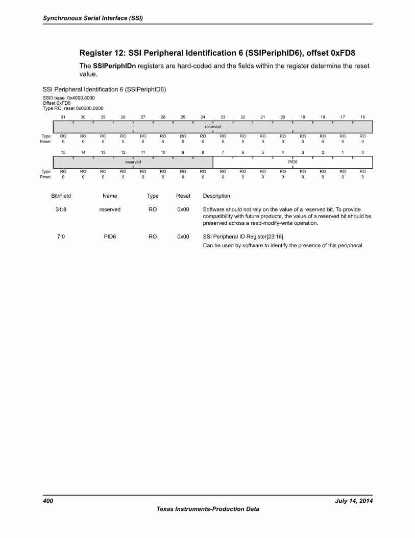
Register 12: SSI Peripheral Identification 6 (SSIPeriphID6), offset 0xFD8The SSIPeriphIDn registers are hard-coded and the fields within the register determine the resetvalue.
SSI Peripheral Identification 6 (SSIPeriphID6)SSI0 base: 0x4000.8000Offset 0xFD8Type RO, reset 0x0000.0000
16171819202122232425262728293031
reserved
ROROROROROROROROROROROROROROROROType0000000000000000Reset
0123456789101112131415
PID6reserved
ROROROROROROROROROROROROROROROROType0000000000000000Reset
DescriptionResetTypeNameBit/Field
Software should not rely on the value of a reserved bit. To providecompatibility with future products, the value of a reserved bit should bepreserved across a read-modify-write operation.
0x00ROreserved31:8
SSI Peripheral ID Register[23:16]Can be used by software to identify the presence of this peripheral.
0x00ROPID67:0
July 14, 2014400Texas Instruments-Production Data
Synchronous Serial Interface (SSI)

Register 13: SSI Peripheral Identification 7 (SSIPeriphID7), offset 0xFDCThe SSIPeriphIDn registers are hard-coded and the fields within the register determine the resetvalue.
SSI Peripheral Identification 7 (SSIPeriphID7)SSI0 base: 0x4000.8000Offset 0xFDCType RO, reset 0x0000.0000
16171819202122232425262728293031
reserved
ROROROROROROROROROROROROROROROROType0000000000000000Reset
0123456789101112131415
PID7reserved
ROROROROROROROROROROROROROROROROType0000000000000000Reset
DescriptionResetTypeNameBit/Field
Software should not rely on the value of a reserved bit. To providecompatibility with future products, the value of a reserved bit should bepreserved across a read-modify-write operation.
0x00ROreserved31:8
SSI Peripheral ID Register[31:24]Can be used by software to identify the presence of this peripheral.
0x00ROPID77:0
401July 14, 2014Texas Instruments-Production Data
Stellaris® LM3S601 Microcontroller
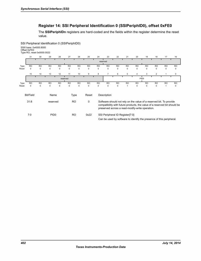
Register 14: SSI Peripheral Identification 0 (SSIPeriphID0), offset 0xFE0The SSIPeriphIDn registers are hard-coded and the fields within the register determine the resetvalue.
SSI Peripheral Identification 0 (SSIPeriphID0)SSI0 base: 0x4000.8000Offset 0xFE0Type RO, reset 0x0000.0022
16171819202122232425262728293031
reserved
ROROROROROROROROROROROROROROROROType0000000000000000Reset
0123456789101112131415
PID0reserved
ROROROROROROROROROROROROROROROROType0100010000000000Reset
DescriptionResetTypeNameBit/Field
Software should not rely on the value of a reserved bit. To providecompatibility with future products, the value of a reserved bit should bepreserved across a read-modify-write operation.
0ROreserved31:8
SSI Peripheral ID Register[7:0]Can be used by software to identify the presence of this peripheral.
0x22ROPID07:0
July 14, 2014402Texas Instruments-Production Data
Synchronous Serial Interface (SSI)

Register 15: SSI Peripheral Identification 1 (SSIPeriphID1), offset 0xFE4The SSIPeriphIDn registers are hard-coded and the fields within the register determine the resetvalue.
SSI Peripheral Identification 1 (SSIPeriphID1)SSI0 base: 0x4000.8000Offset 0xFE4Type RO, reset 0x0000.0000
16171819202122232425262728293031
reserved
ROROROROROROROROROROROROROROROROType0000000000000000Reset
0123456789101112131415
PID1reserved
ROROROROROROROROROROROROROROROROType0000000000000000Reset
DescriptionResetTypeNameBit/Field
Software should not rely on the value of a reserved bit. To providecompatibility with future products, the value of a reserved bit should bepreserved across a read-modify-write operation.
0x00ROreserved31:8
SSI Peripheral ID Register [15:8]Can be used by software to identify the presence of this peripheral.
0x00ROPID17:0
403July 14, 2014Texas Instruments-Production Data
Stellaris® LM3S601 Microcontroller

Register 16: SSI Peripheral Identification 2 (SSIPeriphID2), offset 0xFE8The SSIPeriphIDn registers are hard-coded and the fields within the register determine the resetvalue.
SSI Peripheral Identification 2 (SSIPeriphID2)SSI0 base: 0x4000.8000Offset 0xFE8Type RO, reset 0x0000.0018
16171819202122232425262728293031
reserved
ROROROROROROROROROROROROROROROROType0000000000000000Reset
0123456789101112131415
PID2reserved
ROROROROROROROROROROROROROROROROType0001100000000000Reset
DescriptionResetTypeNameBit/Field
Software should not rely on the value of a reserved bit. To providecompatibility with future products, the value of a reserved bit should bepreserved across a read-modify-write operation.
0x00ROreserved31:8
SSI Peripheral ID Register [23:16]Can be used by software to identify the presence of this peripheral.
0x18ROPID27:0
July 14, 2014404Texas Instruments-Production Data
Synchronous Serial Interface (SSI)
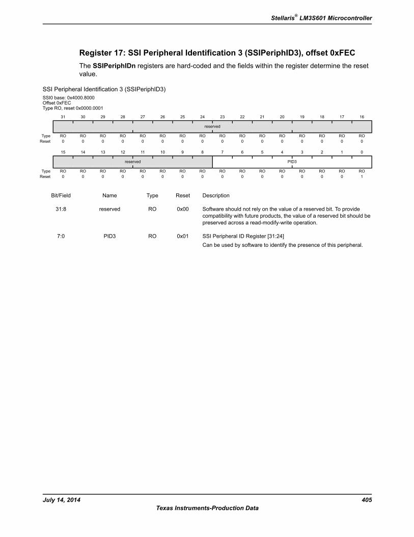
Register 17: SSI Peripheral Identification 3 (SSIPeriphID3), offset 0xFECThe SSIPeriphIDn registers are hard-coded and the fields within the register determine the resetvalue.
SSI Peripheral Identification 3 (SSIPeriphID3)SSI0 base: 0x4000.8000Offset 0xFECType RO, reset 0x0000.0001
16171819202122232425262728293031
reserved
ROROROROROROROROROROROROROROROROType0000000000000000Reset
0123456789101112131415
PID3reserved
ROROROROROROROROROROROROROROROROType1000000000000000Reset
DescriptionResetTypeNameBit/Field
Software should not rely on the value of a reserved bit. To providecompatibility with future products, the value of a reserved bit should bepreserved across a read-modify-write operation.
0x00ROreserved31:8
SSI Peripheral ID Register [31:24]Can be used by software to identify the presence of this peripheral.
0x01ROPID37:0
405July 14, 2014Texas Instruments-Production Data
Stellaris® LM3S601 Microcontroller
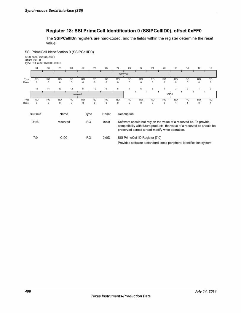
Register 18: SSI PrimeCell Identification 0 (SSIPCellID0), offset 0xFF0The SSIPCellIDn registers are hard-coded, and the fields within the register determine the resetvalue.
SSI PrimeCell Identification 0 (SSIPCellID0)SSI0 base: 0x4000.8000Offset 0xFF0Type RO, reset 0x0000.000D
16171819202122232425262728293031
reserved
ROROROROROROROROROROROROROROROROType0000000000000000Reset
0123456789101112131415
CID0reserved
ROROROROROROROROROROROROROROROROType1011000000000000Reset
DescriptionResetTypeNameBit/Field
Software should not rely on the value of a reserved bit. To providecompatibility with future products, the value of a reserved bit should bepreserved across a read-modify-write operation.
0x00ROreserved31:8
SSI PrimeCell ID Register [7:0]Provides software a standard cross-peripheral identification system.
0x0DROCID07:0
July 14, 2014406Texas Instruments-Production Data
Synchronous Serial Interface (SSI)

Register 19: SSI PrimeCell Identification 1 (SSIPCellID1), offset 0xFF4The SSIPCellIDn registers are hard-coded, and the fields within the register determine the resetvalue.
SSI PrimeCell Identification 1 (SSIPCellID1)SSI0 base: 0x4000.8000Offset 0xFF4Type RO, reset 0x0000.00F0
16171819202122232425262728293031
reserved
ROROROROROROROROROROROROROROROROType0000000000000000Reset
0123456789101112131415
CID1reserved
ROROROROROROROROROROROROROROROROType0000111100000000Reset
DescriptionResetTypeNameBit/Field
Software should not rely on the value of a reserved bit. To providecompatibility with future products, the value of a reserved bit should bepreserved across a read-modify-write operation.
0x00ROreserved31:8
SSI PrimeCell ID Register [15:8]Provides software a standard cross-peripheral identification system.
0xF0ROCID17:0
407July 14, 2014Texas Instruments-Production Data
Stellaris® LM3S601 Microcontroller

Register 20: SSI PrimeCell Identification 2 (SSIPCellID2), offset 0xFF8The SSIPCellIDn registers are hard-coded, and the fields within the register determine the resetvalue.
SSI PrimeCell Identification 2 (SSIPCellID2)SSI0 base: 0x4000.8000Offset 0xFF8Type RO, reset 0x0000.0005
16171819202122232425262728293031
reserved
ROROROROROROROROROROROROROROROROType0000000000000000Reset
0123456789101112131415
CID2reserved
ROROROROROROROROROROROROROROROROType1010000000000000Reset
DescriptionResetTypeNameBit/Field
Software should not rely on the value of a reserved bit. To providecompatibility with future products, the value of a reserved bit should bepreserved across a read-modify-write operation.
0x00ROreserved31:8
SSI PrimeCell ID Register [23:16]Provides software a standard cross-peripheral identification system.
0x05ROCID27:0
July 14, 2014408Texas Instruments-Production Data
Synchronous Serial Interface (SSI)

Register 21: SSI PrimeCell Identification 3 (SSIPCellID3), offset 0xFFCThe SSIPCellIDn registers are hard-coded, and the fields within the register determine the resetvalue.
SSI PrimeCell Identification 3 (SSIPCellID3)SSI0 base: 0x4000.8000Offset 0xFFCType RO, reset 0x0000.00B1
16171819202122232425262728293031
reserved
ROROROROROROROROROROROROROROROROType0000000000000000Reset
0123456789101112131415
CID3reserved
ROROROROROROROROROROROROROROROROType1000110100000000Reset
DescriptionResetTypeNameBit/Field
Software should not rely on the value of a reserved bit. To providecompatibility with future products, the value of a reserved bit should bepreserved across a read-modify-write operation.
0x00ROreserved31:8
SSI PrimeCell ID Register [31:24]Provides software a standard cross-peripheral identification system.
0xB1ROCID37:0
409July 14, 2014Texas Instruments-Production Data
Stellaris® LM3S601 Microcontroller
12 Inter-Integrated Circuit (I2C) InterfaceThe Inter-Integrated Circuit (I2C) bus provides bi-directional data transfer through a two-wire design(a serial data line SDA and a serial clock line SCL), and interfaces to external I2C devices such asserial memory (RAMs and ROMs), networking devices, LCDs, tone generators, and so on. The I2Cbus may also be used for system testing and diagnostic purposes in product development andmanufacture. The LM3S601 microcontroller includes one I2Cmodule, providing the ability to interact(both send and receive) with other I2C devices on the bus.
The Stellaris® I2C interface has the following features:
Devices on the I2C bus can be designated as either a master or a slave
– Supports both sending and receiving data as either a master or a slave
– Supports simultaneous master and slave operation
Four I2C modes
– Master transmit
– Master receive
– Slave transmit
– Slave receive
Two transmission speeds: Standard (100 Kbps) and Fast (400 Kbps)
Master and slave interrupt generation
– Master generates interrupts when a transmit or receive operation completes (or aborts dueto an error)
– Slave generates interrupts when data has been sent or requested by a master
Master with arbitration and clock synchronization, multimaster support, and 7-bit addressingmode
July 14, 2014410Texas Instruments-Production Data
Inter-Integrated Circuit (I2C) Interface

12.1 Block Diagram
Figure 12-1. I2C Block Diagram
I2C I/O Select
I2C Master Core
Interrupt
I2C Slave Core
I2CSCL
I2CSDA
I2CSDA
I2CSCL
I2CSDA
I2CSCL
I2CMSA
I2CMCS
I2CMDR
I2CMTPR
I2CMIMR
I2CMRIS
I2CMICR
I2CMCR
I2CSOAR
I2CSCSR
I2CSDR
I2CSIM
I2CSRIS
I2CSMIS
I2CSICRI2CMMIS
I2C Control
12.2 Signal DescriptionTable 12-1 on page 411 lists the external signals of the I2C interface and describes the function ofeach. The I2C interface signals are alternate functions for some GPIO signals and default to beGPIO signals at reset., with the exception of the I2C0SCL and I2CSDA pins which default to theI2C function. The column in the table below titled "Pin Assignment" lists the possible GPIO pinplacements for the I2C signals. The AFSEL bit in theGPIOAlternate Function Select (GPIOAFSEL)register (page 250) should be set to choose the I2C function. Note that the I2C pins should be set toopen drain using the GPIO Open Drain Select (GPIOODR) register. For more information onconfiguring GPIOs, see “General-Purpose Input/Outputs (GPIOs)” on page 230.
Table 12-1. I2C Signals (48QFP)
DescriptionBuffer TypeaPin TypePin NumberPin Name
I2C clock.ODI/O33I2CSCL
I2C data.ODI/O34I2CSDA
a. The TTL designation indicates the pin has TTL-compatible voltage levels.
12.3 Functional DescriptionI2C module is comprised of both master and slave functions which are implemented as separateperipherals. For proper operation, the SDA and SCL pins must be connected to bi-directionalopen-drain pads. A typical I2C bus configuration is shown in Figure 12-2 on page 412.
See “Inter-Integrated Circuit (I2C) Interface” on page 535 for I2C timing diagrams.
411July 14, 2014Texas Instruments-Production Data
Stellaris® LM3S601 Microcontroller
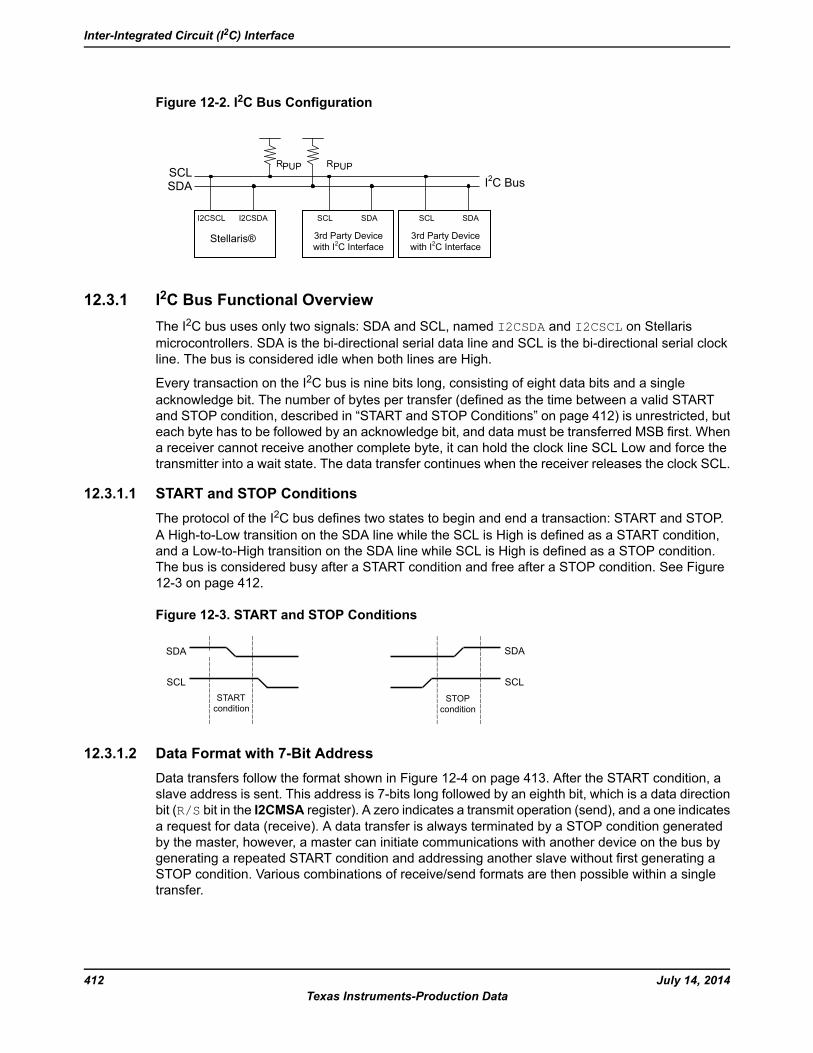
Figure 12-2. I2C Bus Configuration
RPUP
Stellaris®
I2CSCL I2CSDA
RPUP
3rd Party Devicewith I2C Interface
SCL SDA
I2C BusSCLSDA
SCL SDA
3rd Party Devicewith I2C Interface
12.3.1 I2C Bus Functional OverviewThe I2C bus uses only two signals: SDA and SCL, named I2CSDA and I2CSCL on Stellarismicrocontrollers. SDA is the bi-directional serial data line and SCL is the bi-directional serial clockline. The bus is considered idle when both lines are High.
Every transaction on the I2C bus is nine bits long, consisting of eight data bits and a singleacknowledge bit. The number of bytes per transfer (defined as the time between a valid STARTand STOP condition, described in “START and STOP Conditions” on page 412) is unrestricted, buteach byte has to be followed by an acknowledge bit, and data must be transferred MSB first. Whena receiver cannot receive another complete byte, it can hold the clock line SCL Low and force thetransmitter into a wait state. The data transfer continues when the receiver releases the clock SCL.
12.3.1.1 START and STOP ConditionsThe protocol of the I2C bus defines two states to begin and end a transaction: START and STOP.A High-to-Low transition on the SDA line while the SCL is High is defined as a START condition,and a Low-to-High transition on the SDA line while SCL is High is defined as a STOP condition.The bus is considered busy after a START condition and free after a STOP condition. See Figure12-3 on page 412.
Figure 12-3. START and STOP Conditions
STARTcondition
SDA
SCLSTOP
condition
SDA
SCL
12.3.1.2 Data Format with 7-Bit AddressData transfers follow the format shown in Figure 12-4 on page 413. After the START condition, aslave address is sent. This address is 7-bits long followed by an eighth bit, which is a data directionbit (R/S bit in the I2CMSA register). A zero indicates a transmit operation (send), and a one indicatesa request for data (receive). A data transfer is always terminated by a STOP condition generatedby the master, however, a master can initiate communications with another device on the bus bygenerating a repeated START condition and addressing another slave without first generating aSTOP condition. Various combinations of receive/send formats are then possible within a singletransfer.
July 14, 2014412Texas Instruments-Production Data
Inter-Integrated Circuit (I2C) Interface
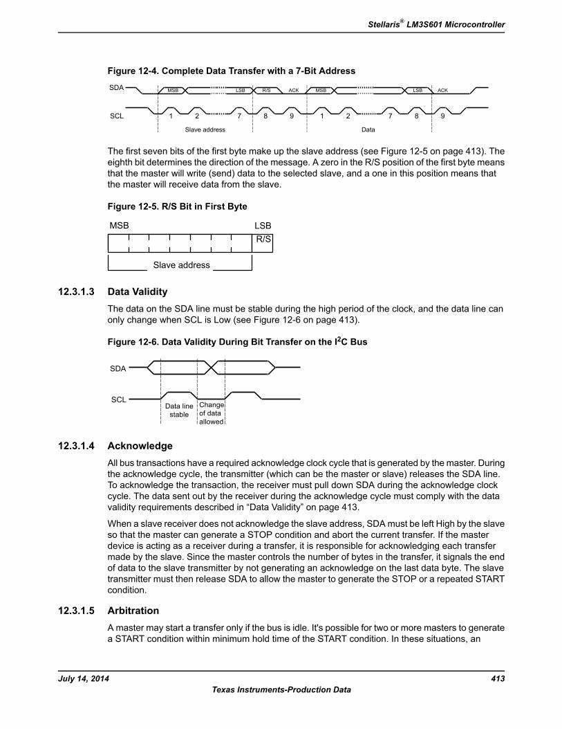
Figure 12-4. Complete Data Transfer with a 7-Bit Address
DataSlave address
ACKLSBMSBACKR/SLSBMSBSDA
SCL 1 2 7 8 9 1 2 7 8 9
The first seven bits of the first byte make up the slave address (see Figure 12-5 on page 413). Theeighth bit determines the direction of the message. A zero in the R/S position of the first byte meansthat the master will write (send) data to the selected slave, and a one in this position means thatthe master will receive data from the slave.
Figure 12-5. R/S Bit in First Byte
R/SLSB
Slave address
MSB
12.3.1.3 Data ValidityThe data on the SDA line must be stable during the high period of the clock, and the data line canonly change when SCL is Low (see Figure 12-6 on page 413).
Figure 12-6. Data Validity During Bit Transfer on the I2C Bus
Changeof dataallowed
Data linestable
SDA
SCL
12.3.1.4 AcknowledgeAll bus transactions have a required acknowledge clock cycle that is generated by the master. Duringthe acknowledge cycle, the transmitter (which can be the master or slave) releases the SDA line.To acknowledge the transaction, the receiver must pull down SDA during the acknowledge clockcycle. The data sent out by the receiver during the acknowledge cycle must comply with the datavalidity requirements described in “Data Validity” on page 413.
When a slave receiver does not acknowledge the slave address, SDAmust be left High by the slaveso that the master can generate a STOP condition and abort the current transfer. If the masterdevice is acting as a receiver during a transfer, it is responsible for acknowledging each transfermade by the slave. Since the master controls the number of bytes in the transfer, it signals the endof data to the slave transmitter by not generating an acknowledge on the last data byte. The slavetransmitter must then release SDA to allow the master to generate the STOP or a repeated STARTcondition.
12.3.1.5 ArbitrationA master may start a transfer only if the bus is idle. It's possible for two or more masters to generatea START condition within minimum hold time of the START condition. In these situations, an
413July 14, 2014Texas Instruments-Production Data
Stellaris® LM3S601 Microcontroller
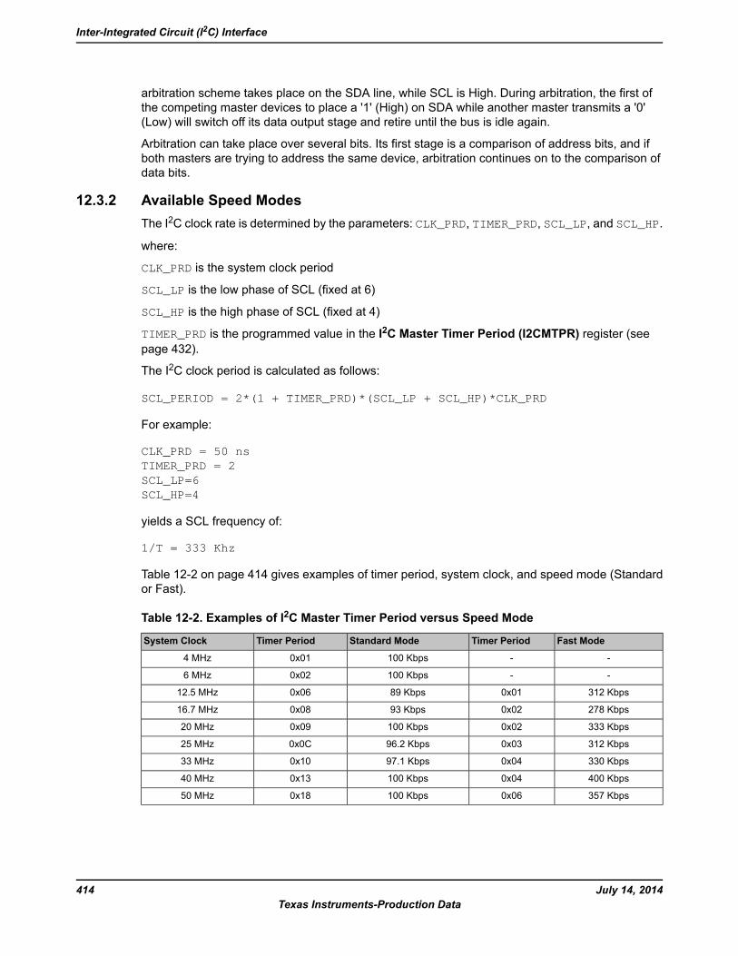
arbitration scheme takes place on the SDA line, while SCL is High. During arbitration, the first ofthe competing master devices to place a '1' (High) on SDA while another master transmits a '0'(Low) will switch off its data output stage and retire until the bus is idle again.
Arbitration can take place over several bits. Its first stage is a comparison of address bits, and ifboth masters are trying to address the same device, arbitration continues on to the comparison ofdata bits.
12.3.2 Available Speed ModesThe I2C clock rate is determined by the parameters: CLK_PRD, TIMER_PRD, SCL_LP, and SCL_HP.
where:
CLK_PRD is the system clock period
SCL_LP is the low phase of SCL (fixed at 6)
SCL_HP is the high phase of SCL (fixed at 4)
TIMER_PRD is the programmed value in the I2C Master Timer Period (I2CMTPR) register (seepage 432).
The I2C clock period is calculated as follows:
SCL_PERIOD = 2*(1 + TIMER_PRD)*(SCL_LP + SCL_HP)*CLK_PRD
For example:
CLK_PRD = 50 nsTIMER_PRD = 2SCL_LP=6SCL_HP=4
yields a SCL frequency of:
1/T = 333 Khz
Table 12-2 on page 414 gives examples of timer period, system clock, and speed mode (Standardor Fast).
Table 12-2. Examples of I2C Master Timer Period versus Speed Mode
Fast ModeTimer PeriodStandard ModeTimer PeriodSystem Clock
--100 Kbps0x014 MHz
--100 Kbps0x026 MHz
312 Kbps0x0189 Kbps0x0612.5 MHz
278 Kbps0x0293 Kbps0x0816.7 MHz
333 Kbps0x02100 Kbps0x0920 MHz
312 Kbps0x0396.2 Kbps0x0C25 MHz
330 Kbps0x0497.1 Kbps0x1033 MHz
400 Kbps0x04100 Kbps0x1340 MHz
357 Kbps0x06100 Kbps0x1850 MHz
July 14, 2014414Texas Instruments-Production Data
Inter-Integrated Circuit (I2C) Interface
12.3.3 InterruptsThe I2C can generate interrupts when the following conditions are observed:
Master transaction completed
Master arbitration lost
Master transaction error
Slave transaction received
Slave transaction requested
There is a separate interrupt signal for the I2C master and I2C slave modules. While both modulescan generate interrupts for multiple conditions, only a single interrupt signal is sent to the interruptcontroller.
12.3.3.1 I2C Master InterruptsThe I2C master module generates an interrupt when a transaction completes (either transmit orreceive), when arbitration is lost, or when an error occurs during a transaction. To enable the I2Cmaster interrupt, software must set the IM bit in the I2CMaster Interrupt Mask (I2CMIMR) register.When an interrupt condition is met, software must check the ERROR and ARBLST bits in the I2CMaster Control/Status (I2CMCS) register to verify that an error didn't occur during the last transactionand to ensure that arbitration has not been lost. An error condition is asserted if the last transactionwasn't acknowledged by the slave. If an error is not detected and the master has not lost arbitration,the application can proceed with the transfer. The interrupt is cleared by writing a 1 to the IC bit inthe I2C Master Interrupt Clear (I2CMICR) register.
If the application doesn't require the use of interrupts, the raw interrupt status is always visible viathe I2C Master Raw Interrupt Status (I2CMRIS) register.
12.3.3.2 I2C Slave InterruptsThe slave module can generate an interrupt when data has been received or requested. This interruptis enabled by writing a 1 to the DATAIM bit in the I2C Slave Interrupt Mask (I2CSIMR) register.Software determines whether the module should write (transmit) or read (receive) data from the I2CSlave Data (I2CSDR) register, by checking the RREQ and TREQ bits of the I2C Slave Control/Status(I2CSCSR) register. If the slave module is in receive mode and the first byte of a transfer is received,the FBR bit is set along with the RREQ bit. The interrupt is cleared by writing a 1 to the DATAIC bitin the I2C Slave Interrupt Clear (I2CSICR) register.
If the application doesn't require the use of interrupts, the raw interrupt status is always visible viathe I2C Slave Raw Interrupt Status (I2CSRIS) register.
12.3.4 Loopback OperationThe I2C modules can be placed into an internal loopback mode for diagnostic or debug work. Thisis accomplished by setting the LPBK bit in the I2C Master Configuration (I2CMCR) register. Inloopback mode, the SDA and SCL signals from the master and slave modules are tied together.
12.3.5 Command Sequence Flow ChartsThis section details the steps required to perform the various I2C transfer types in both master andslave mode.
415July 14, 2014Texas Instruments-Production Data
Stellaris® LM3S601 Microcontroller
12.3.5.1 I2C Master Command SequencesThe figures that follow show the command sequences available for the I2C master.
July 14, 2014416Texas Instruments-Production Data
Inter-Integrated Circuit (I2C) Interface
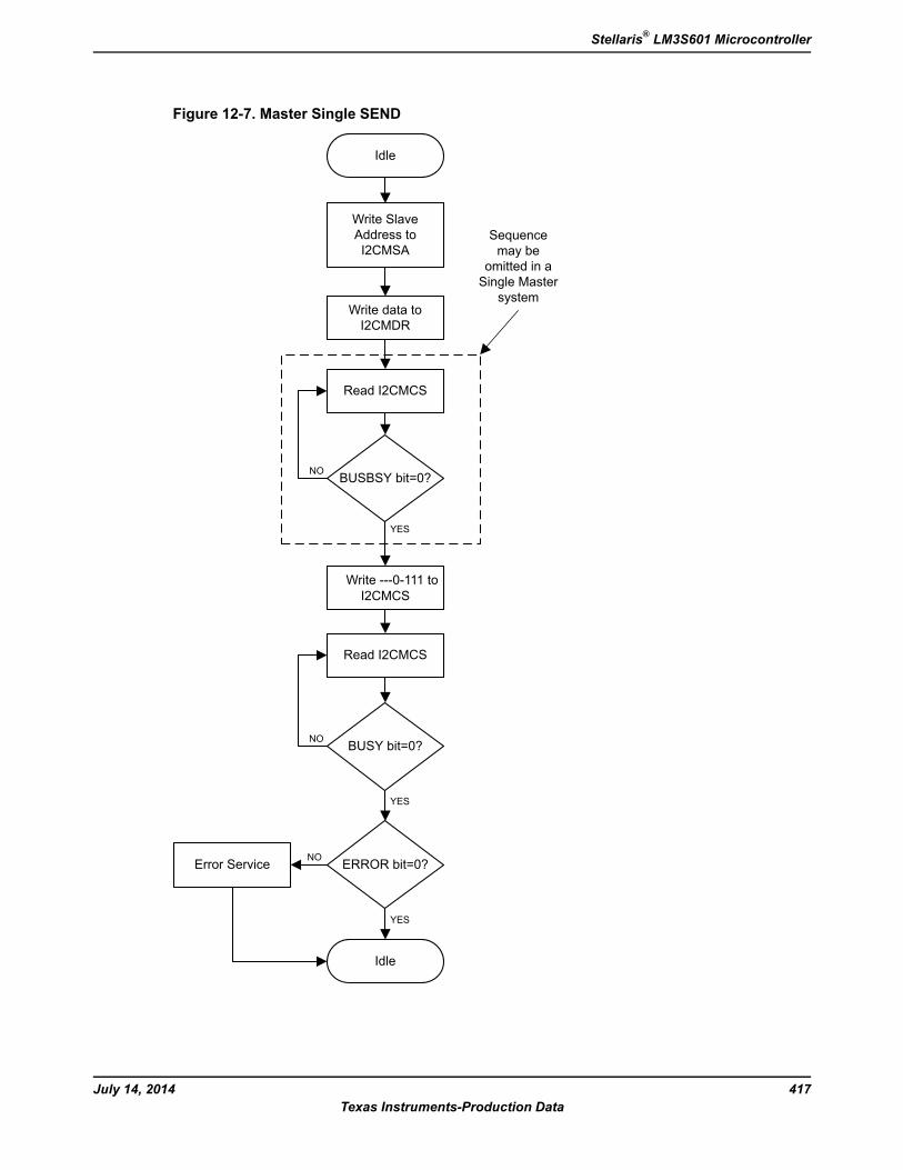
Figure 12-7. Master Single SEND
Idle
Write SlaveAddress toI2CMSA
Write data toI2CMDR
Read I2CMCS
Sequencemay be
omitted in aSingle Master
system
BUSBSY bit=0?NO
Write ---0-111 toI2CMCS
YES
Read I2CMCS
BUSY bit=0?
ERROR bit=0?
YES
Error Service
Idle
YES
NO
NO
417July 14, 2014Texas Instruments-Production Data
Stellaris® LM3S601 Microcontroller
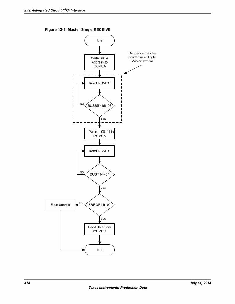
Figure 12-8. Master Single RECEIVE
Idle
Write SlaveAddress toI2CMSA
Read I2CMCS
Sequence may beomitted in a SingleMaster system
BUSBSY bit=0?NO
Write ---00111 toI2CMCS
YES
Read I2CMCS
BUSY bit=0?
ERROR bit=0?
YES
Error Service
Idle
NO
NO
Read data fromI2CMDR
YES
July 14, 2014418Texas Instruments-Production Data
Inter-Integrated Circuit (I2C) Interface
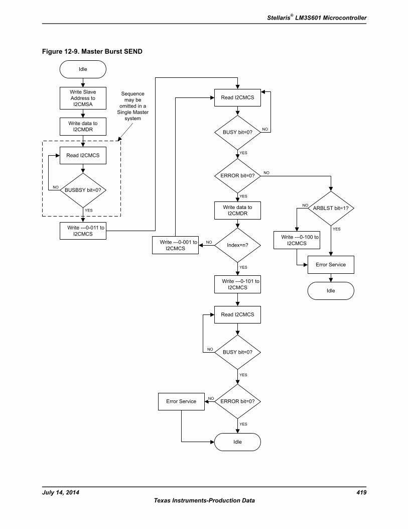
Figure 12-9. Master Burst SEND
Idle
Write SlaveAddress toI2CMSA
Write data toI2CMDR
Read I2CMCS
BUSBSY bit=0?
YES
Write ---0-011 toI2CMCS
NO
Read I2CMCS
BUSY bit=0?
YES
ERROR bit=0?
YES
ARBLST bit=1?Write data toI2CMDR
Write ---0-100 toI2CMCSIndex=n?
NO
Error Service
Idle
YES
Write ---0-001 toI2CMCS
Write ---0-101 toI2CMCS
YES
Read I2CMCS
BUSY bit=0?
ERROR bit=0?
YES
NO
Idle
YES
Error Service NO
NO
NO
NO
Sequencemay be
omitted in aSingle Master
system
419July 14, 2014Texas Instruments-Production Data
Stellaris® LM3S601 Microcontroller
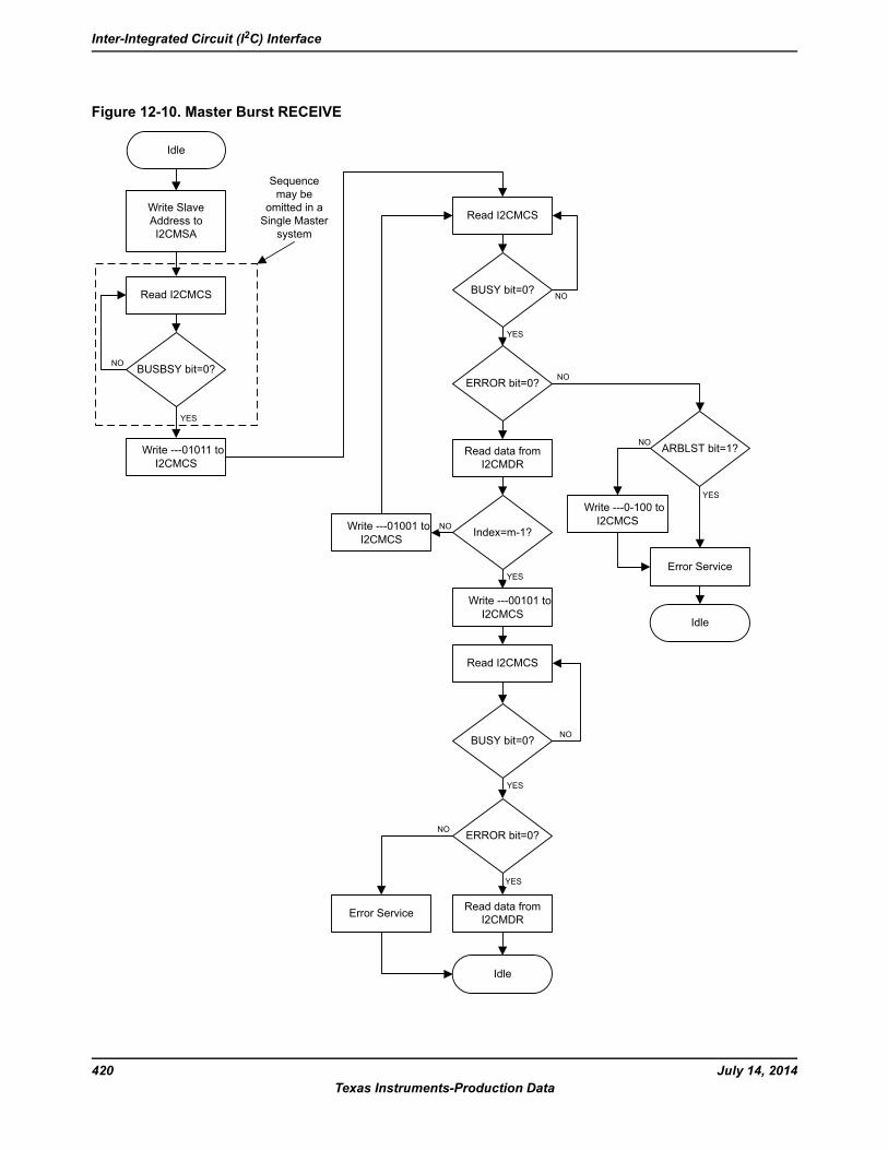
Figure 12-10. Master Burst RECEIVE
Idle
Write SlaveAddress toI2CMSA
Read I2CMCS
BUSBSY bit=0?NO
Write ---01011 toI2CMCS
YES
Read I2CMCS
BUSY bit=0? NO
ERROR bit=0?
YES
ARBLST bit=1?
Write ---0-100 toI2CMCS
NO
Error Service
YES
Idle
Read data fromI2CMDR
Index=m-1?
Write ---00101 toI2CMCS
YES
Idle
Read data fromI2CMDRError Service
ERROR bit=0?
YES
Write ---01001 toI2CMCS
Read I2CMCS
BUSY bit=0? NO
YES
Sequencemay be
omitted in aSingle Master
system
NO
NO
NO
July 14, 2014420Texas Instruments-Production Data
Inter-Integrated Circuit (I2C) Interface
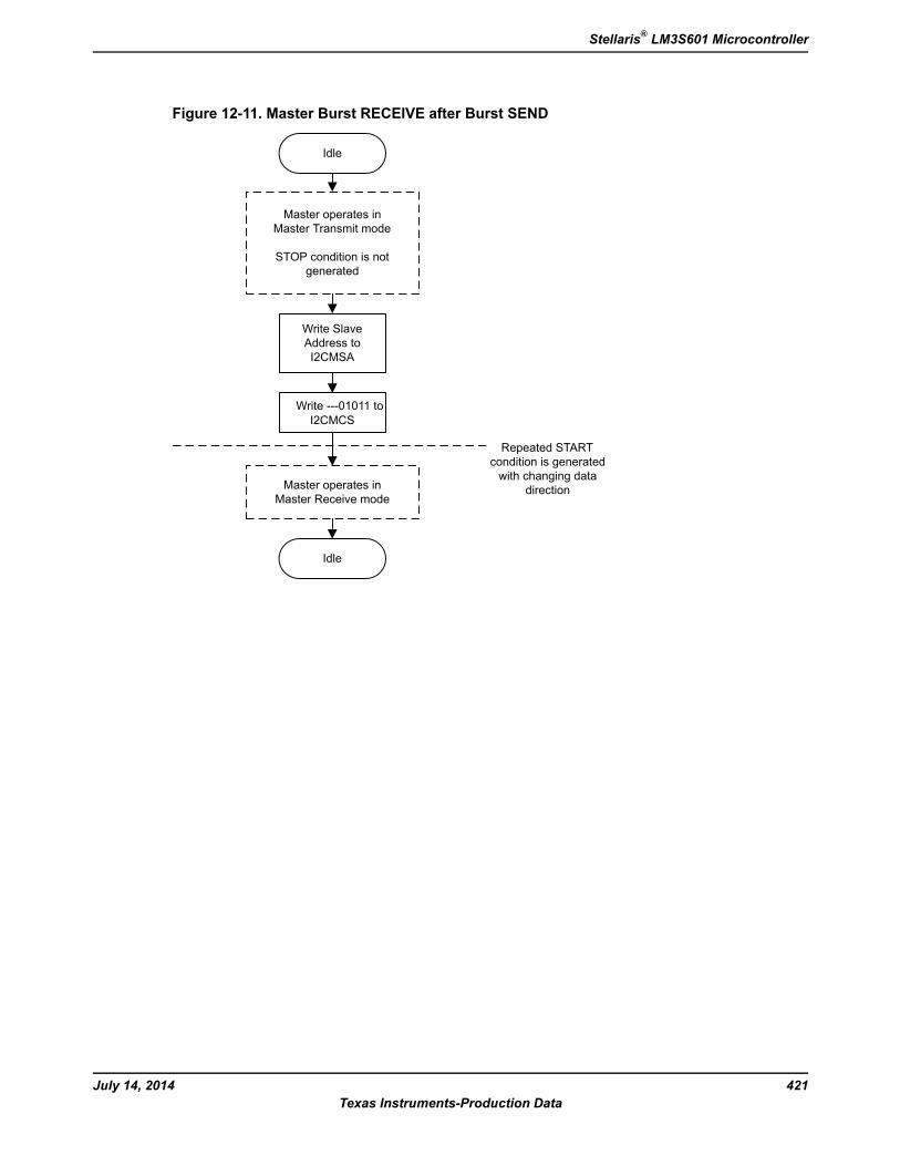
Figure 12-11. Master Burst RECEIVE after Burst SEND
Idle
Master operates inMaster Transmit mode
STOP condition is notgenerated
Write SlaveAddress toI2CMSA
Write ---01011 toI2CMCS
Master operates inMaster Receive mode
Idle
Repeated STARTcondition is generatedwith changing data
direction
421July 14, 2014Texas Instruments-Production Data
Stellaris® LM3S601 Microcontroller
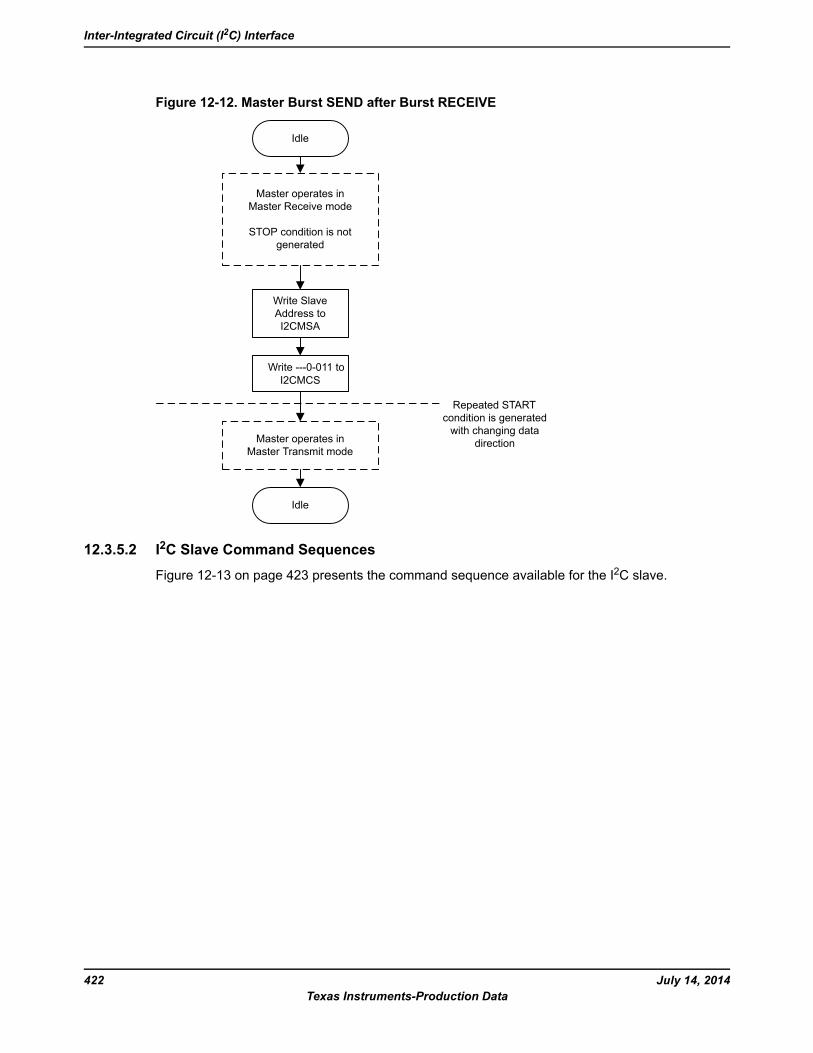
Figure 12-12. Master Burst SEND after Burst RECEIVE
Idle
Master operates inMaster Receive mode
STOP condition is notgenerated
Write SlaveAddress toI2CMSA
Write ---0-011 toI2CMCS
Master operates inMaster Transmit mode
Idle
Repeated STARTcondition is generatedwith changing data
direction
12.3.5.2 I2C Slave Command SequencesFigure 12-13 on page 423 presents the command sequence available for the I2C slave.
July 14, 2014422Texas Instruments-Production Data
Inter-Integrated Circuit (I2C) Interface
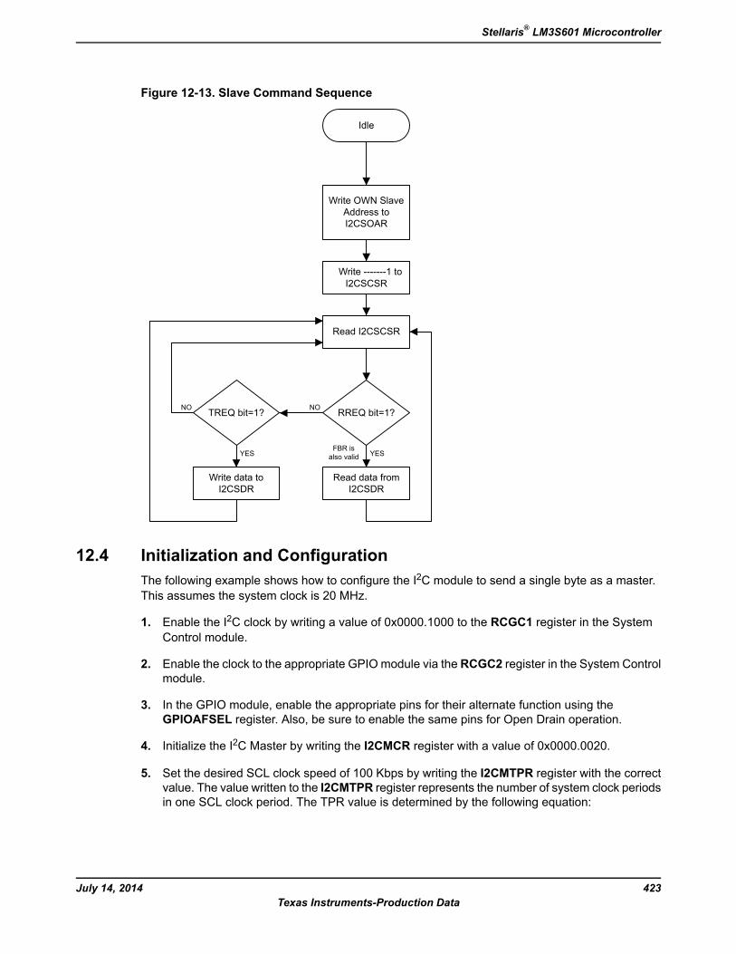
Figure 12-13. Slave Command Sequence
Idle
Write OWN SlaveAddress toI2CSOAR
Write -------1 toI2CSCSR
Read I2CSCSR
RREQ bit=1?
Read data fromI2CSDR
YES
TREQ bit=1? NO
Write data toI2CSDR
YES
NO
FBR isalso valid
12.4 Initialization and ConfigurationThe following example shows how to configure the I2C module to send a single byte as a master.This assumes the system clock is 20 MHz.
1. Enable the I2C clock by writing a value of 0x0000.1000 to the RCGC1 register in the SystemControl module.
2. Enable the clock to the appropriate GPIO module via the RCGC2 register in the System Controlmodule.
3. In the GPIO module, enable the appropriate pins for their alternate function using theGPIOAFSEL register. Also, be sure to enable the same pins for Open Drain operation.
4. Initialize the I2C Master by writing the I2CMCR register with a value of 0x0000.0020.
5. Set the desired SCL clock speed of 100 Kbps by writing the I2CMTPR register with the correctvalue. The value written to the I2CMTPR register represents the number of system clock periodsin one SCL clock period. The TPR value is determined by the following equation:
423July 14, 2014Texas Instruments-Production Data
Stellaris® LM3S601 Microcontroller
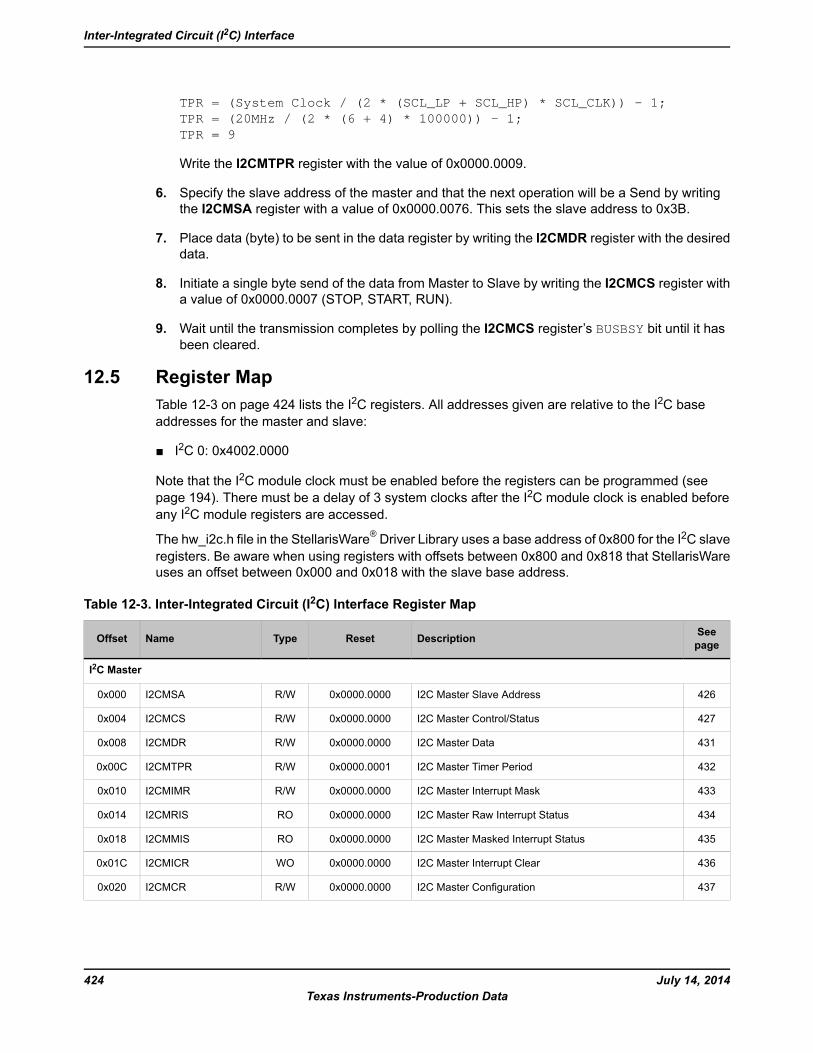
TPR = (System Clock / (2 * (SCL_LP + SCL_HP) * SCL_CLK)) - 1;TPR = (20MHz / (2 * (6 + 4) * 100000)) - 1;TPR = 9
Write the I2CMTPR register with the value of 0x0000.0009.
6. Specify the slave address of the master and that the next operation will be a Send by writingthe I2CMSA register with a value of 0x0000.0076. This sets the slave address to 0x3B.
7. Place data (byte) to be sent in the data register by writing the I2CMDR register with the desireddata.
8. Initiate a single byte send of the data from Master to Slave by writing the I2CMCS register witha value of 0x0000.0007 (STOP, START, RUN).
9. Wait until the transmission completes by polling the I2CMCS register’s BUSBSY bit until it hasbeen cleared.
12.5 Register MapTable 12-3 on page 424 lists the I2C registers. All addresses given are relative to the I2C baseaddresses for the master and slave:
I2C 0: 0x4002.0000
Note that the I2C module clock must be enabled before the registers can be programmed (seepage 194). There must be a delay of 3 system clocks after the I2C module clock is enabled beforeany I2C module registers are accessed.
The hw_i2c.h file in the StellarisWare® Driver Library uses a base address of 0x800 for the I2C slaveregisters. Be aware when using registers with offsets between 0x800 and 0x818 that StellarisWareuses an offset between 0x000 and 0x018 with the slave base address.
Table 12-3. Inter-Integrated Circuit (I2C) Interface Register Map
SeepageDescriptionResetTypeNameOffset
I2C Master
426I2C Master Slave Address0x0000.0000R/WI2CMSA0x000
427I2C Master Control/Status0x0000.0000R/WI2CMCS0x004
431I2C Master Data0x0000.0000R/WI2CMDR0x008
432I2C Master Timer Period0x0000.0001R/WI2CMTPR0x00C
433I2C Master Interrupt Mask0x0000.0000R/WI2CMIMR0x010
434I2C Master Raw Interrupt Status0x0000.0000ROI2CMRIS0x014
435I2C Master Masked Interrupt Status0x0000.0000ROI2CMMIS0x018
436I2C Master Interrupt Clear0x0000.0000WOI2CMICR0x01C
437I2C Master Configuration0x0000.0000R/WI2CMCR0x020
July 14, 2014424Texas Instruments-Production Data
Inter-Integrated Circuit (I2C) Interface
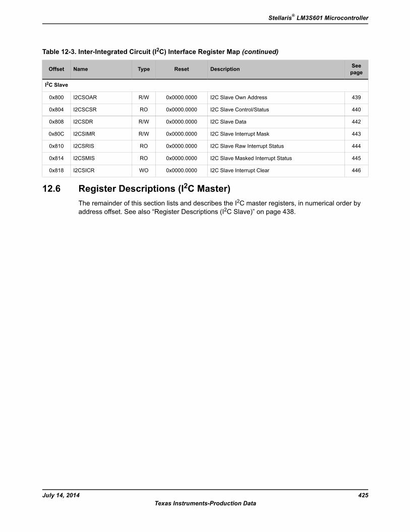
Table 12-3. Inter-Integrated Circuit (I2C) Interface Register Map (continued)
SeepageDescriptionResetTypeNameOffset
I2C Slave
439I2C Slave Own Address0x0000.0000R/WI2CSOAR0x800
440I2C Slave Control/Status0x0000.0000ROI2CSCSR0x804
442I2C Slave Data0x0000.0000R/WI2CSDR0x808
443I2C Slave Interrupt Mask0x0000.0000R/WI2CSIMR0x80C
444I2C Slave Raw Interrupt Status0x0000.0000ROI2CSRIS0x810
445I2C Slave Masked Interrupt Status0x0000.0000ROI2CSMIS0x814
446I2C Slave Interrupt Clear0x0000.0000WOI2CSICR0x818
12.6 Register Descriptions (I2C Master)The remainder of this section lists and describes the I2C master registers, in numerical order byaddress offset. See also “Register Descriptions (I2C Slave)” on page 438.
425July 14, 2014Texas Instruments-Production Data
Stellaris® LM3S601 Microcontroller
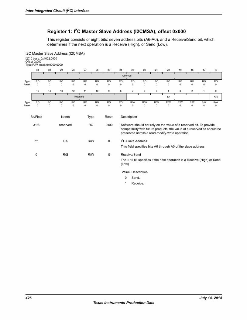
Register 1: I2C Master Slave Address (I2CMSA), offset 0x000This register consists of eight bits: seven address bits (A6-A0), and a Receive/Send bit, whichdetermines if the next operation is a Receive (High), or Send (Low).
I2C Master Slave Address (I2CMSA)I2C 0 base: 0x4002.0000Offset 0x000Type R/W, reset 0x0000.0000
16171819202122232425262728293031
reserved
ROROROROROROROROROROROROROROROROType0000000000000000Reset
0123456789101112131415
R/SSAreserved
R/WR/WR/WR/WR/WR/WR/WR/WROROROROROROROROType0000000000000000Reset
DescriptionResetTypeNameBit/Field
Software should not rely on the value of a reserved bit. To providecompatibility with future products, the value of a reserved bit should bepreserved across a read-modify-write operation.
0x00ROreserved31:8
I2C Slave Address
This field specifies bits A6 through A0 of the slave address.
0R/WSA7:1
Receive/SendThe R/S bit specifies if the next operation is a Receive (High) or Send(Low).
DescriptionValue
Send.0
Receive.1
0R/WR/S0
July 14, 2014426Texas Instruments-Production Data
Inter-Integrated Circuit (I2C) Interface
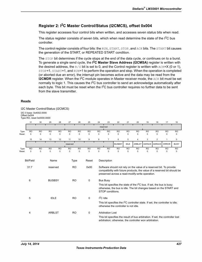
Register 2: I2C Master Control/Status (I2CMCS), offset 0x004This register accesses four control bits when written, and accesses seven status bits when read.
The status register consists of seven bits, which when read determine the state of the I2C buscontroller.
The control register consists of four bits: the RUN, START, STOP, and ACK bits. The START bit causesthe generation of the START, or REPEATED START condition.
The STOP bit determines if the cycle stops at the end of the data cycle, or continues on to a burst.To generate a single send cycle, the I2C Master Slave Address (I2CMSA) register is written withthe desired address, the R/S bit is set to 0, and the Control register is written with ACK=X (0 or 1),STOP=1, START=1, and RUN=1 to perform the operation and stop. When the operation is completed(or aborted due an error), the interrupt pin becomes active and the data may be read from theI2CMDR register. When the I2C module operates in Master receiver mode, the ACK bit must be setnormally to logic 1. This causes the I2C bus controller to send an acknowledge automatically aftereach byte. This bit must be reset when the I2C bus controller requires no further data to be sentfrom the slave transmitter.
Reads
I2C Master Control/Status (I2CMCS)I2C 0 base: 0x4002.0000Offset 0x004Type RO, reset 0x0000.0000
16171819202122232425262728293031
reserved
ROROROROROROROROROROROROROROROROType0000000000000000Reset
0123456789101112131415
BUSYERRORADRACKDATACKARBLSTIDLEBUSBSYreserved
ROROROROROROROROROROROROROROROROType0000000000000000Reset
DescriptionResetTypeNameBit/Field
Software should not rely on the value of a reserved bit. To providecompatibility with future products, the value of a reserved bit should bepreserved across a read-modify-write operation.
0x00ROreserved31:7
Bus BusyThis bit specifies the state of the I2C bus. If set, the bus is busy;otherwise, the bus is idle. The bit changes based on the START andSTOP conditions.
0ROBUSBSY6
I2C Idle
This bit specifies the I2C controller state. If set, the controller is idle;otherwise the controller is not idle.
0ROIDLE5
Arbitration LostThis bit specifies the result of bus arbitration. If set, the controller lostarbitration; otherwise, the controller won arbitration.
0ROARBLST4
427July 14, 2014Texas Instruments-Production Data
Stellaris® LM3S601 Microcontroller
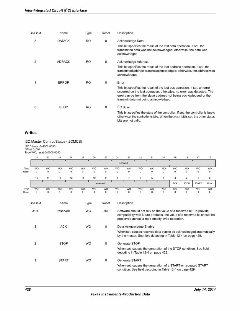
DescriptionResetTypeNameBit/Field
Acknowledge DataThis bit specifies the result of the last data operation. If set, thetransmitted data was not acknowledged; otherwise, the data wasacknowledged.
0RODATACK3
Acknowledge AddressThis bit specifies the result of the last address operation. If set, thetransmitted address was not acknowledged; otherwise, the address wasacknowledged.
0ROADRACK2
ErrorThis bit specifies the result of the last bus operation. If set, an erroroccurred on the last operation; otherwise, no error was detected. Theerror can be from the slave address not being acknowledged or thetransmit data not being acknowledged.
0ROERROR1
I2C Busy
This bit specifies the state of the controller. If set, the controller is busy;otherwise, the controller is idle. When the BUSY bit is set, the other statusbits are not valid.
0ROBUSY0
Writes
I2C Master Control/Status (I2CMCS)I2C 0 base: 0x4002.0000Offset 0x004Type WO, reset 0x0000.0000
16171819202122232425262728293031
reserved
WOWOWOWOWOWOWOWOWOWOWOWOWOWOWOWOType0000000000000000Reset
0123456789101112131415
RUNSTARTSTOPACKreserved
WOWOWOWOWOWOWOWOWOWOWOWOWOWOWOWOType0000000000000000Reset
DescriptionResetTypeNameBit/Field
Software should not rely on the value of a reserved bit. To providecompatibility with future products, the value of a reserved bit should bepreserved across a read-modify-write operation.
0x00WOreserved31:4
Data Acknowledge EnableWhen set, causes received data byte to be acknowledged automaticallyby the master. See field decoding in Table 12-4 on page 429.
0WOACK3
Generate STOPWhen set, causes the generation of the STOP condition. See fielddecoding in Table 12-4 on page 429.
0WOSTOP2
Generate STARTWhen set, causes the generation of a START or repeated STARTcondition. See field decoding in Table 12-4 on page 429.
0WOSTART1
July 14, 2014428Texas Instruments-Production Data
Inter-Integrated Circuit (I2C) Interface
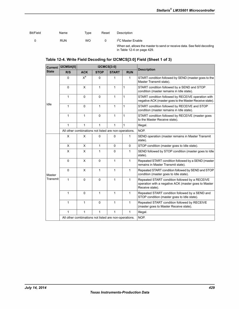
DescriptionResetTypeNameBit/Field
I2C Master Enable
When set, allows the master to send or receive data. See field decodingin Table 12-4 on page 429.
0WORUN0
Table 12-4. Write Field Decoding for I2CMCS[3:0] Field (Sheet 1 of 3)
DescriptionI2CMCS[3:0]I2CMSA[0]Current
State RUNSTARTSTOPACKR/S
START condition followed by SEND (master goes to theMaster Transmit state).
110Xa0
Idle
START condition followed by a SEND and STOPcondition (master remains in Idle state).
111X0
START condition followed by RECEIVE operation withnegative ACK (master goes to theMaster Receive state).
11001
START condition followed by RECEIVE and STOPcondition (master remains in Idle state).
11101
START condition followed by RECEIVE (master goesto the Master Receive state).
11011
Illegal.11111
NOP.All other combinations not listed are non-operations.
SEND operation (master remains in Master Transmitstate).
100XX
MasterTransmit
STOP condition (master goes to Idle state).001XX
SEND followed by STOP condition (master goes to Idlestate).
101XX
Repeated START condition followed by a SEND (masterremains in Master Transmit state).
110X0
Repeated START condition followed by SENDand STOPcondition (master goes to Idle state).
111X0
Repeated START condition followed by a RECEIVEoperation with a negative ACK (master goes to MasterReceive state).
11001
Repeated START condition followed by a SEND andSTOP condition (master goes to Idle state).
11101
Repeated START condition followed by RECEIVE(master goes to Master Receive state).
11011
Illegal.11111
NOP.All other combinations not listed are non-operations.
429July 14, 2014Texas Instruments-Production Data
Stellaris® LM3S601 Microcontroller
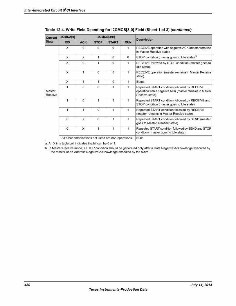
Table 12-4. Write Field Decoding for I2CMCS[3:0] Field (Sheet 1 of 3) (continued)
DescriptionI2CMCS[3:0]I2CMSA[0]Current
State RUNSTARTSTOPACKR/S
RECEIVE operation with negative ACK (master remainsin Master Receive state).
1000X
MasterReceive
STOP condition (master goes to Idle state).b001XX
RECEIVE followed by STOP condition (master goes toIdle state).
1010X
RECEIVE operation (master remains in Master Receivestate).
1001X
Illegal.1011X
Repeated START condition followed by RECEIVEoperation with a negative ACK (master remains in MasterReceive state).
11001
Repeated START condition followed by RECEIVE andSTOP condition (master goes to Idle state).
11101
Repeated START condition followed by RECEIVE(master remains in Master Receive state).
11011
Repeated START condition followed by SEND (mastergoes to Master Transmit state).
110X0
Repeated START condition followed by SENDand STOPcondition (master goes to Idle state).
111X0
NOP.All other combinations not listed are non-operations.
a. An X in a table cell indicates the bit can be 0 or 1.b. In Master Receive mode, a STOP condition should be generated only after a Data Negative Acknowledge executed by
the master or an Address Negative Acknowledge executed by the slave.
July 14, 2014430Texas Instruments-Production Data
Inter-Integrated Circuit (I2C) Interface
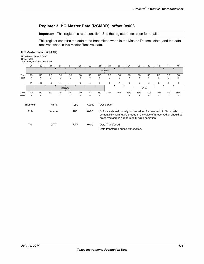
Register 3: I2C Master Data (I2CMDR), offset 0x008
Important: This register is read-sensitive. See the register description for details.
This register contains the data to be transmitted when in the Master Transmit state, and the datareceived when in the Master Receive state.
I2C Master Data (I2CMDR)I2C 0 base: 0x4002.0000Offset 0x008Type R/W, reset 0x0000.0000
16171819202122232425262728293031
reserved
ROROROROROROROROROROROROROROROROType0000000000000000Reset
0123456789101112131415
DATAreserved
R/WR/WR/WR/WR/WR/WR/WR/WROROROROROROROROType0000000000000000Reset
DescriptionResetTypeNameBit/Field
Software should not rely on the value of a reserved bit. To providecompatibility with future products, the value of a reserved bit should bepreserved across a read-modify-write operation.
0x00ROreserved31:8
Data TransferredData transferred during transaction.
0x00R/WDATA7:0
431July 14, 2014Texas Instruments-Production Data
Stellaris® LM3S601 Microcontroller
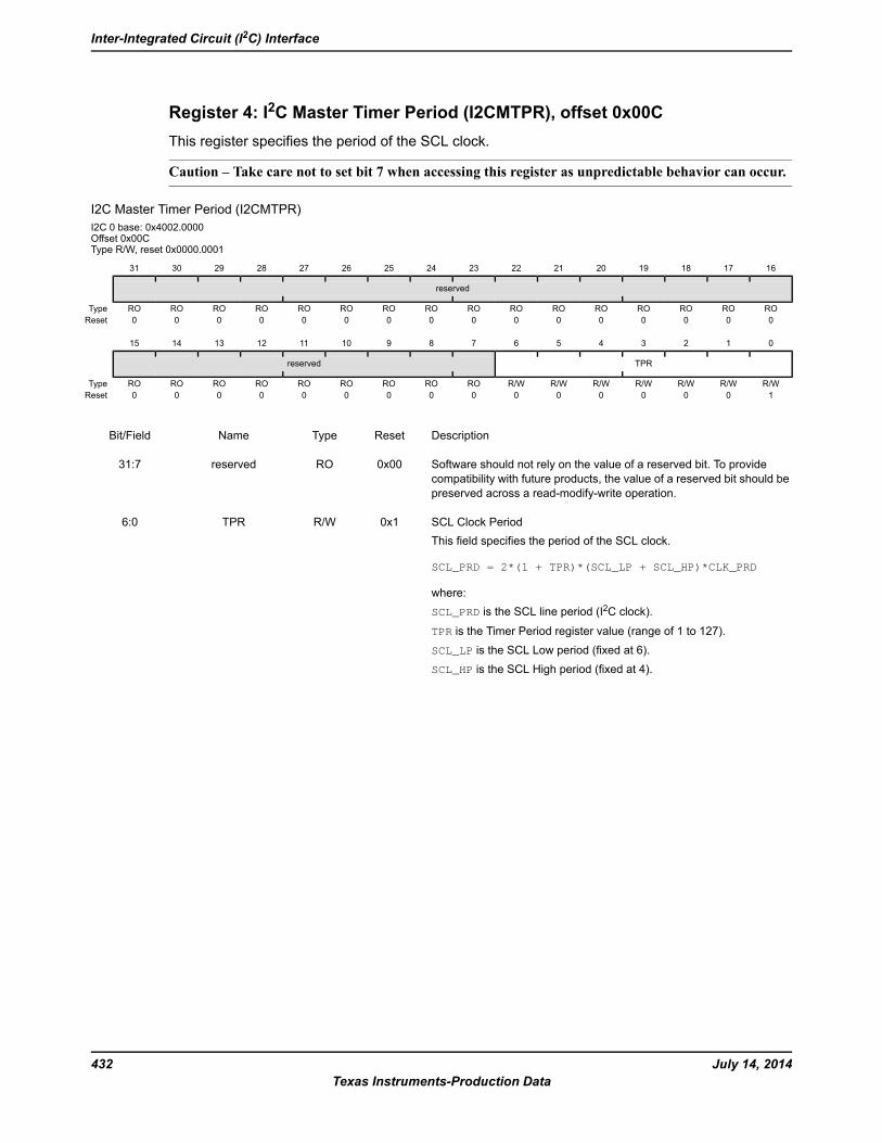
Register 4: I2C Master Timer Period (I2CMTPR), offset 0x00CThis register specifies the period of the SCL clock.
Caution – Take care not to set bit 7 when accessing this register as unpredictable behavior can occur.
I2C Master Timer Period (I2CMTPR)I2C 0 base: 0x4002.0000Offset 0x00CType R/W, reset 0x0000.0001
16171819202122232425262728293031
reserved
ROROROROROROROROROROROROROROROROType0000000000000000Reset
0123456789101112131415
TPRreserved
R/WR/WR/WR/WR/WR/WR/WROROROROROROROROROType1000000000000000Reset
DescriptionResetTypeNameBit/Field
Software should not rely on the value of a reserved bit. To providecompatibility with future products, the value of a reserved bit should bepreserved across a read-modify-write operation.
0x00ROreserved31:7
SCL Clock PeriodThis field specifies the period of the SCL clock.
SCL_PRD = 2*(1 + TPR)*(SCL_LP + SCL_HP)*CLK_PRD
where:SCL_PRD is the SCL line period (I2C clock).
TPR is the Timer Period register value (range of 1 to 127).SCL_LP is the SCL Low period (fixed at 6).SCL_HP is the SCL High period (fixed at 4).
0x1R/WTPR6:0
July 14, 2014432Texas Instruments-Production Data
Inter-Integrated Circuit (I2C) Interface
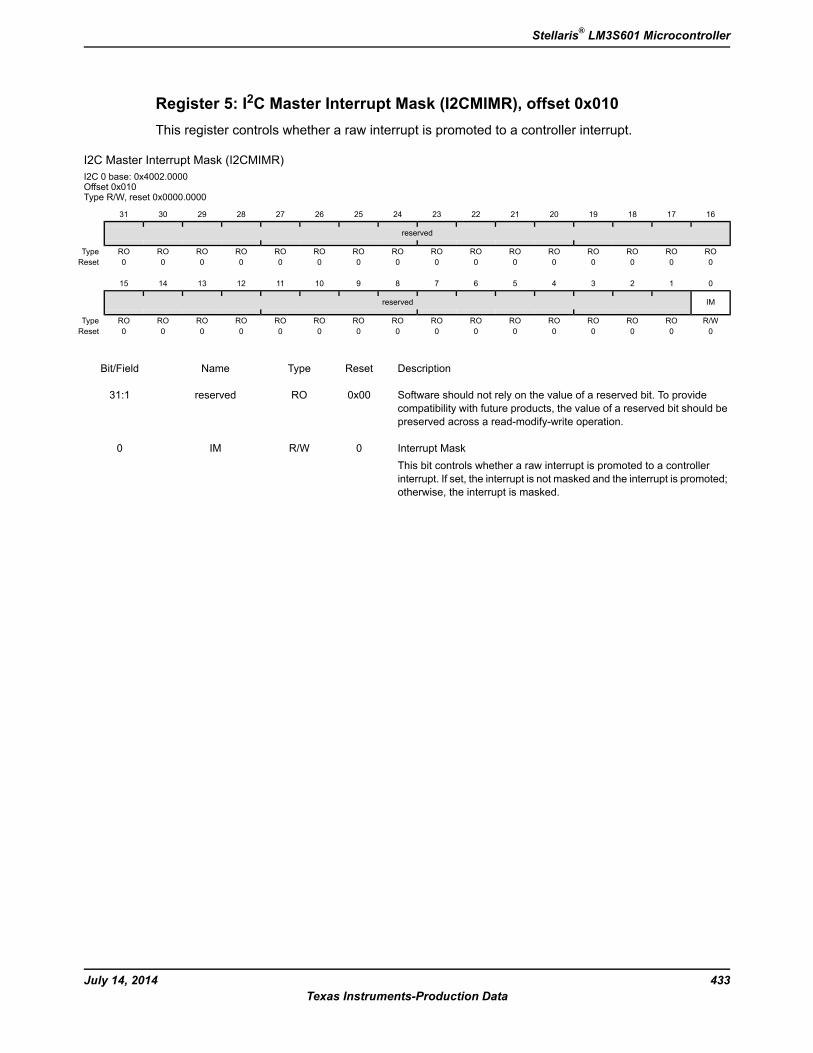
Register 5: I2C Master Interrupt Mask (I2CMIMR), offset 0x010This register controls whether a raw interrupt is promoted to a controller interrupt.
I2C Master Interrupt Mask (I2CMIMR)I2C 0 base: 0x4002.0000Offset 0x010Type R/W, reset 0x0000.0000
16171819202122232425262728293031
reserved
ROROROROROROROROROROROROROROROROType0000000000000000Reset
0123456789101112131415
IMreserved
R/WROROROROROROROROROROROROROROROType0000000000000000Reset
DescriptionResetTypeNameBit/Field
Software should not rely on the value of a reserved bit. To providecompatibility with future products, the value of a reserved bit should bepreserved across a read-modify-write operation.
0x00ROreserved31:1
Interrupt MaskThis bit controls whether a raw interrupt is promoted to a controllerinterrupt. If set, the interrupt is not masked and the interrupt is promoted;otherwise, the interrupt is masked.
0R/WIM0
433July 14, 2014Texas Instruments-Production Data
Stellaris® LM3S601 Microcontroller
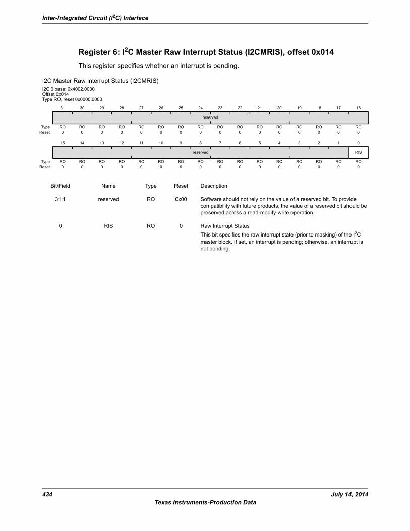
Register 6: I2C Master Raw Interrupt Status (I2CMRIS), offset 0x014This register specifies whether an interrupt is pending.
I2C Master Raw Interrupt Status (I2CMRIS)I2C 0 base: 0x4002.0000Offset 0x014Type RO, reset 0x0000.0000
16171819202122232425262728293031
reserved
ROROROROROROROROROROROROROROROROType0000000000000000Reset
0123456789101112131415
RISreserved
ROROROROROROROROROROROROROROROROType0000000000000000Reset
DescriptionResetTypeNameBit/Field
Software should not rely on the value of a reserved bit. To providecompatibility with future products, the value of a reserved bit should bepreserved across a read-modify-write operation.
0x00ROreserved31:1
Raw Interrupt StatusThis bit specifies the raw interrupt state (prior to masking) of the I2Cmaster block. If set, an interrupt is pending; otherwise, an interrupt isnot pending.
0RORIS0
July 14, 2014434Texas Instruments-Production Data
Inter-Integrated Circuit (I2C) Interface
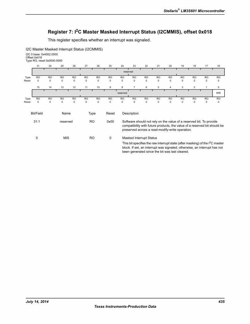
Register 7: I2C Master Masked Interrupt Status (I2CMMIS), offset 0x018This register specifies whether an interrupt was signaled.
I2C Master Masked Interrupt Status (I2CMMIS)I2C 0 base: 0x4002.0000Offset 0x018Type RO, reset 0x0000.0000
16171819202122232425262728293031
reserved
ROROROROROROROROROROROROROROROROType0000000000000000Reset
0123456789101112131415
MISreserved
ROROROROROROROROROROROROROROROROType0000000000000000Reset
DescriptionResetTypeNameBit/Field
Software should not rely on the value of a reserved bit. To providecompatibility with future products, the value of a reserved bit should bepreserved across a read-modify-write operation.
0x00ROreserved31:1
Masked Interrupt StatusThis bit specifies the raw interrupt state (after masking) of the I2Cmasterblock. If set, an interrupt was signaled; otherwise, an interrupt has notbeen generated since the bit was last cleared.
0ROMIS0
435July 14, 2014Texas Instruments-Production Data
Stellaris® LM3S601 Microcontroller
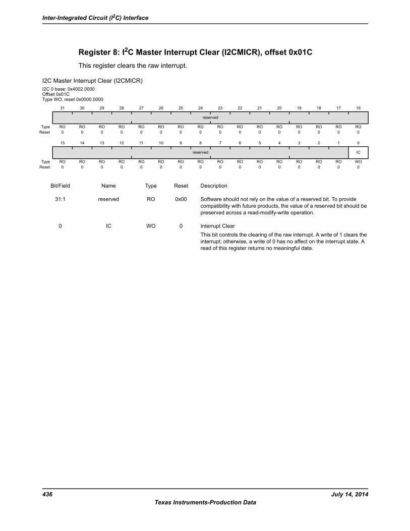
Register 8: I2C Master Interrupt Clear (I2CMICR), offset 0x01CThis register clears the raw interrupt.
I2C Master Interrupt Clear (I2CMICR)I2C 0 base: 0x4002.0000Offset 0x01CType WO, reset 0x0000.0000
16171819202122232425262728293031
reserved
ROROROROROROROROROROROROROROROROType0000000000000000Reset
0123456789101112131415
ICreserved
WOROROROROROROROROROROROROROROROType0000000000000000Reset
DescriptionResetTypeNameBit/Field
Software should not rely on the value of a reserved bit. To providecompatibility with future products, the value of a reserved bit should bepreserved across a read-modify-write operation.
0x00ROreserved31:1
Interrupt ClearThis bit controls the clearing of the raw interrupt. A write of 1 clears theinterrupt; otherwise, a write of 0 has no affect on the interrupt state. Aread of this register returns no meaningful data.
0WOIC0
July 14, 2014436Texas Instruments-Production Data
Inter-Integrated Circuit (I2C) Interface
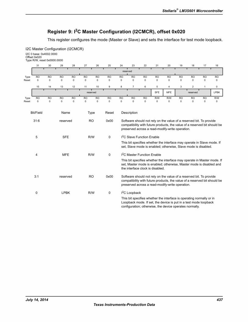
Register 9: I2C Master Configuration (I2CMCR), offset 0x020This register configures the mode (Master or Slave) and sets the interface for test mode loopback.
I2C Master Configuration (I2CMCR)I2C 0 base: 0x4002.0000Offset 0x020Type R/W, reset 0x0000.0000
16171819202122232425262728293031
reserved
ROROROROROROROROROROROROROROROROType0000000000000000Reset
0123456789101112131415
LPBKreservedMFESFEreserved
R/WROROROR/WR/WROROROROROROROROROROType0000000000000000Reset
DescriptionResetTypeNameBit/Field
Software should not rely on the value of a reserved bit. To providecompatibility with future products, the value of a reserved bit should bepreserved across a read-modify-write operation.
0x00ROreserved31:6
I2C Slave Function Enable
This bit specifies whether the interface may operate in Slave mode. Ifset, Slave mode is enabled; otherwise, Slave mode is disabled.
0R/WSFE5
I2C Master Function Enable
This bit specifies whether the interface may operate in Master mode. Ifset, Master mode is enabled; otherwise, Master mode is disabled andthe interface clock is disabled.
0R/WMFE4
Software should not rely on the value of a reserved bit. To providecompatibility with future products, the value of a reserved bit should bepreserved across a read-modify-write operation.
0x00ROreserved3:1
I2C Loopback
This bit specifies whether the interface is operating normally or inLoopback mode. If set, the device is put in a test mode loopbackconfiguration; otherwise, the device operates normally.
0R/WLPBK0
437July 14, 2014Texas Instruments-Production Data
Stellaris® LM3S601 Microcontroller
12.7 Register Descriptions (I2C Slave)The remainder of this section lists and describes the I2C slave registers, in numerical order byaddress offset. See also “Register Descriptions (I2C Master)” on page 425.
July 14, 2014438Texas Instruments-Production Data
Inter-Integrated Circuit (I2C) Interface
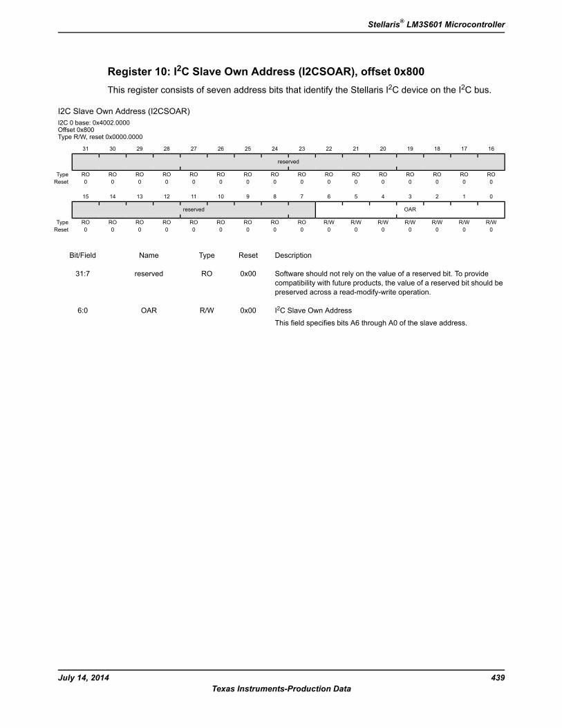
Register 10: I2C Slave Own Address (I2CSOAR), offset 0x800This register consists of seven address bits that identify the Stellaris I2C device on the I2C bus.
I2C Slave Own Address (I2CSOAR)I2C 0 base: 0x4002.0000Offset 0x800Type R/W, reset 0x0000.0000
16171819202122232425262728293031
reserved
ROROROROROROROROROROROROROROROROType0000000000000000Reset
0123456789101112131415
OARreserved
R/WR/WR/WR/WR/WR/WR/WROROROROROROROROROType0000000000000000Reset
DescriptionResetTypeNameBit/Field
Software should not rely on the value of a reserved bit. To providecompatibility with future products, the value of a reserved bit should bepreserved across a read-modify-write operation.
0x00ROreserved31:7
I2C Slave Own Address
This field specifies bits A6 through A0 of the slave address.
0x00R/WOAR6:0
439July 14, 2014Texas Instruments-Production Data
Stellaris® LM3S601 Microcontroller
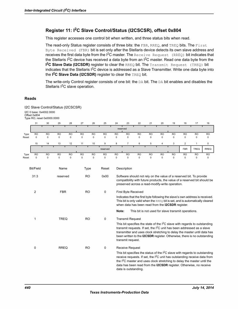
Register 11: I2C Slave Control/Status (I2CSCSR), offset 0x804This register accesses one control bit when written, and three status bits when read.
The read-only Status register consists of three bits: the FBR, RREQ, and TREQ bits. The FirstByte Received (FBR) bit is set only after the Stellaris device detects its own slave address andreceives the first data byte from the I2C master. The Receive Request (RREQ) bit indicates thatthe Stellaris I2C device has received a data byte from an I2C master. Read one data byte from theI2C Slave Data (I2CSDR) register to clear the RREQ bit. The Transmit Request (TREQ) bitindicates that the Stellaris I2C device is addressed as a Slave Transmitter. Write one data byte intothe I2C Slave Data (I2CSDR) register to clear the TREQ bit.
The write-only Control register consists of one bit: the DA bit. The DA bit enables and disables theStellaris I2C slave operation.
Reads
I2C Slave Control/Status (I2CSCSR)I2C 0 base: 0x4002.0000Offset 0x804Type RO, reset 0x0000.0000
16171819202122232425262728293031
reserved
ROROROROROROROROROROROROROROROROType0000000000000000Reset
0123456789101112131415
RREQTREQFBRreserved
ROROROROROROROROROROROROROROROROType0000000000000000Reset
DescriptionResetTypeNameBit/Field
Software should not rely on the value of a reserved bit. To providecompatibility with future products, the value of a reserved bit should bepreserved across a read-modify-write operation.
0x00ROreserved31:3
First Byte ReceivedIndicates that the first byte following the slave’s own address is received.This bit is only valid when the RREQ bit is set, and is automatically clearedwhen data has been read from the I2CSDR register.
Note: This bit is not used for slave transmit operations.
0ROFBR2
Transmit RequestThis bit specifies the state of the I2C slave with regards to outstandingtransmit requests. If set, the I2C unit has been addressed as a slavetransmitter and uses clock stretching to delay the master until data hasbeen written to the I2CSDR register. Otherwise, there is no outstandingtransmit request.
0ROTREQ1
Receive RequestThis bit specifies the status of the I2C slave with regards to outstandingreceive requests. If set, the I2C unit has outstanding receive data fromthe I2C master and uses clock stretching to delay the master until thedata has been read from the I2CSDR register. Otherwise, no receivedata is outstanding.
0RORREQ0
July 14, 2014440Texas Instruments-Production Data
Inter-Integrated Circuit (I2C) Interface
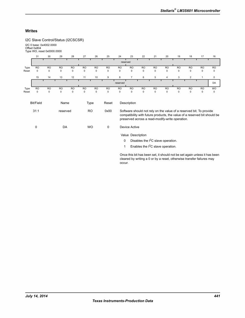
Writes
I2C Slave Control/Status (I2CSCSR)I2C 0 base: 0x4002.0000Offset 0x804Type WO, reset 0x0000.0000
16171819202122232425262728293031
reserved
ROROROROROROROROROROROROROROROROType0000000000000000Reset
0123456789101112131415
DAreserved
WOROROROROROROROROROROROROROROROType0000000000000000Reset
DescriptionResetTypeNameBit/Field
Software should not rely on the value of a reserved bit. To providecompatibility with future products, the value of a reserved bit should bepreserved across a read-modify-write operation.
0x00ROreserved31:1
Device Active
DescriptionValue
Disables the I2C slave operation.0
Enables the I2C slave operation.1
Once this bit has been set, it should not be set again unless it has beencleared by writing a 0 or by a reset, otherwise transfer failures mayoccur.
0WODA0
441July 14, 2014Texas Instruments-Production Data
Stellaris® LM3S601 Microcontroller
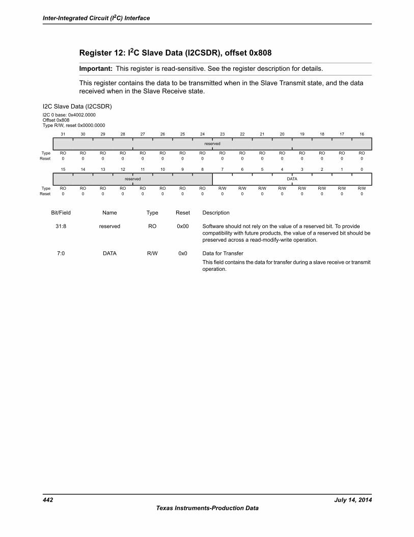
Register 12: I2C Slave Data (I2CSDR), offset 0x808
Important: This register is read-sensitive. See the register description for details.
This register contains the data to be transmitted when in the Slave Transmit state, and the datareceived when in the Slave Receive state.
I2C Slave Data (I2CSDR)I2C 0 base: 0x4002.0000Offset 0x808Type R/W, reset 0x0000.0000
16171819202122232425262728293031
reserved
ROROROROROROROROROROROROROROROROType0000000000000000Reset
0123456789101112131415
DATAreserved
R/WR/WR/WR/WR/WR/WR/WR/WROROROROROROROROType0000000000000000Reset
DescriptionResetTypeNameBit/Field
Software should not rely on the value of a reserved bit. To providecompatibility with future products, the value of a reserved bit should bepreserved across a read-modify-write operation.
0x00ROreserved31:8
Data for TransferThis field contains the data for transfer during a slave receive or transmitoperation.
0x0R/WDATA7:0
July 14, 2014442Texas Instruments-Production Data
Inter-Integrated Circuit (I2C) Interface
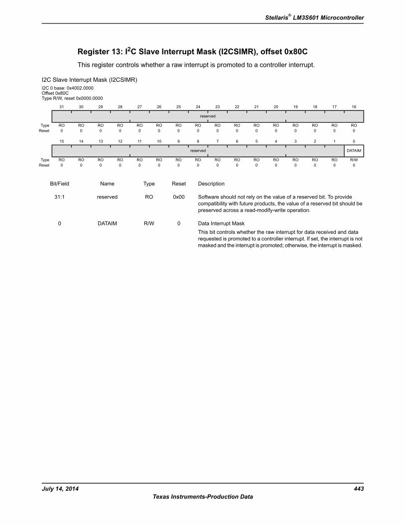
Register 13: I2C Slave Interrupt Mask (I2CSIMR), offset 0x80CThis register controls whether a raw interrupt is promoted to a controller interrupt.
I2C Slave Interrupt Mask (I2CSIMR)I2C 0 base: 0x4002.0000Offset 0x80CType R/W, reset 0x0000.0000
16171819202122232425262728293031
reserved
ROROROROROROROROROROROROROROROROType0000000000000000Reset
0123456789101112131415
DATAIMreserved
R/WROROROROROROROROROROROROROROROType0000000000000000Reset
DescriptionResetTypeNameBit/Field
Software should not rely on the value of a reserved bit. To providecompatibility with future products, the value of a reserved bit should bepreserved across a read-modify-write operation.
0x00ROreserved31:1
Data Interrupt MaskThis bit controls whether the raw interrupt for data received and datarequested is promoted to a controller interrupt. If set, the interrupt is notmasked and the interrupt is promoted; otherwise, the interrupt is masked.
0R/WDATAIM0
443July 14, 2014Texas Instruments-Production Data
Stellaris® LM3S601 Microcontroller
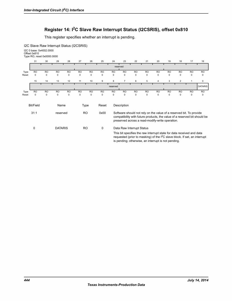
Register 14: I2C Slave Raw Interrupt Status (I2CSRIS), offset 0x810This register specifies whether an interrupt is pending.
I2C Slave Raw Interrupt Status (I2CSRIS)I2C 0 base: 0x4002.0000Offset 0x810Type RO, reset 0x0000.0000
16171819202122232425262728293031
reserved
ROROROROROROROROROROROROROROROROType0000000000000000Reset
0123456789101112131415
DATARISreserved
ROROROROROROROROROROROROROROROROType0000000000000000Reset
DescriptionResetTypeNameBit/Field
Software should not rely on the value of a reserved bit. To providecompatibility with future products, the value of a reserved bit should bepreserved across a read-modify-write operation.
0x00ROreserved31:1
Data Raw Interrupt StatusThis bit specifies the raw interrupt state for data received and datarequested (prior to masking) of the I2C slave block. If set, an interruptis pending; otherwise, an interrupt is not pending.
0RODATARIS0
July 14, 2014444Texas Instruments-Production Data
Inter-Integrated Circuit (I2C) Interface
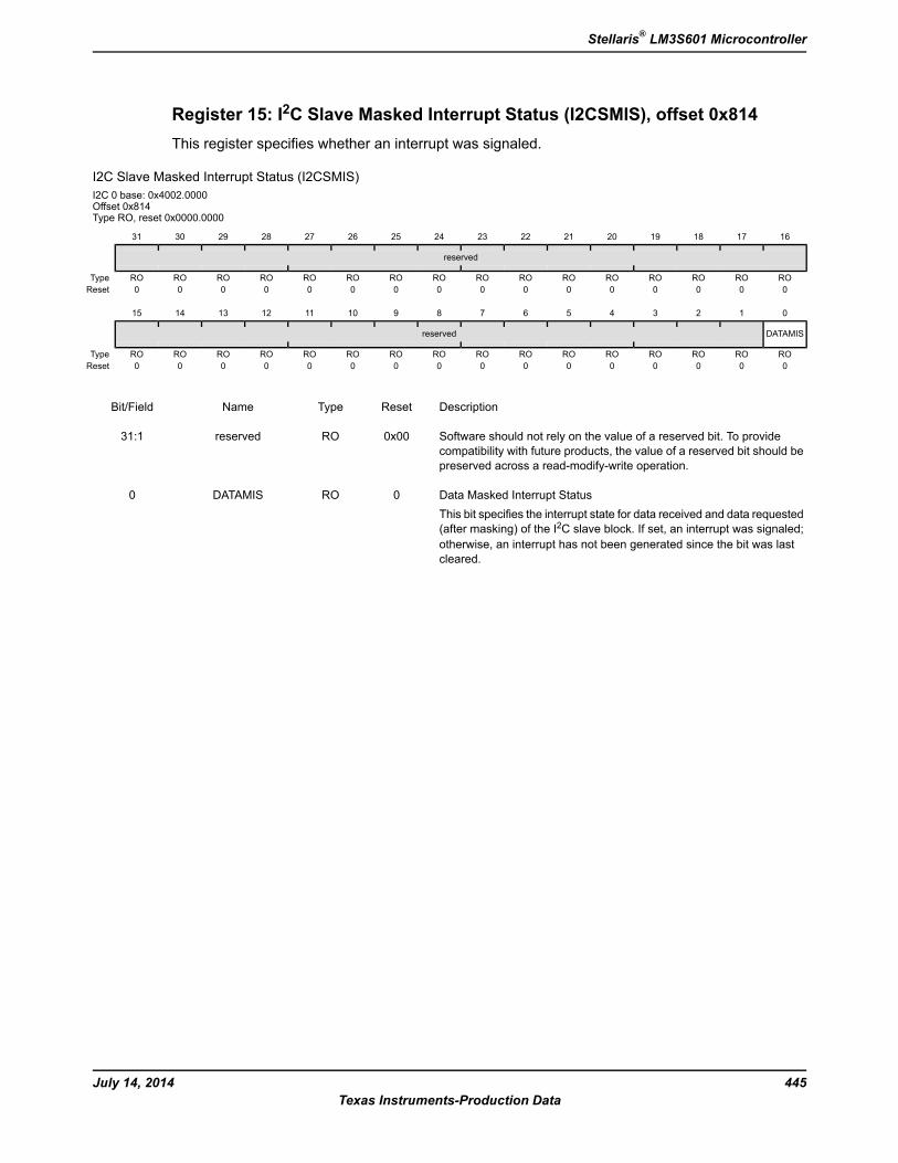
Register 15: I2C Slave Masked Interrupt Status (I2CSMIS), offset 0x814This register specifies whether an interrupt was signaled.
I2C Slave Masked Interrupt Status (I2CSMIS)I2C 0 base: 0x4002.0000Offset 0x814Type RO, reset 0x0000.0000
16171819202122232425262728293031
reserved
ROROROROROROROROROROROROROROROROType0000000000000000Reset
0123456789101112131415
DATAMISreserved
ROROROROROROROROROROROROROROROROType0000000000000000Reset
DescriptionResetTypeNameBit/Field
Software should not rely on the value of a reserved bit. To providecompatibility with future products, the value of a reserved bit should bepreserved across a read-modify-write operation.
0x00ROreserved31:1
Data Masked Interrupt StatusThis bit specifies the interrupt state for data received and data requested(after masking) of the I2C slave block. If set, an interrupt was signaled;otherwise, an interrupt has not been generated since the bit was lastcleared.
0RODATAMIS0
445July 14, 2014Texas Instruments-Production Data
Stellaris® LM3S601 Microcontroller
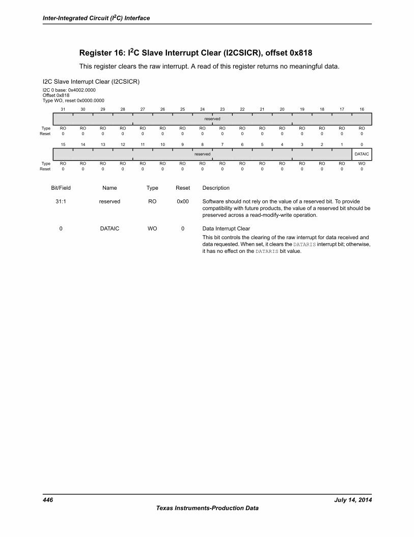
Register 16: I2C Slave Interrupt Clear (I2CSICR), offset 0x818This register clears the raw interrupt. A read of this register returns no meaningful data.
I2C Slave Interrupt Clear (I2CSICR)I2C 0 base: 0x4002.0000Offset 0x818Type WO, reset 0x0000.0000
16171819202122232425262728293031
reserved
ROROROROROROROROROROROROROROROROType0000000000000000Reset
0123456789101112131415
DATAICreserved
WOROROROROROROROROROROROROROROROType0000000000000000Reset
DescriptionResetTypeNameBit/Field
Software should not rely on the value of a reserved bit. To providecompatibility with future products, the value of a reserved bit should bepreserved across a read-modify-write operation.
0x00ROreserved31:1
Data Interrupt ClearThis bit controls the clearing of the raw interrupt for data received anddata requested. When set, it clears the DATARIS interrupt bit; otherwise,it has no effect on the DATARIS bit value.
0WODATAIC0
July 14, 2014446Texas Instruments-Production Data
Inter-Integrated Circuit (I2C) Interface
13 Analog ComparatorsAn analog comparator is a peripheral that compares two analog voltages, and provides a logicaloutput that signals the comparison result.
Note: Not all comparators have the option to drive an output pin. See the Comparator OperatingMode tables in “Functional Description” on page 449 for more information.
The comparator can provide its output to a device pin, acting as a replacement for an analogcomparator on the board, or it can be used to signal the application via interrupts to cause it to startcapturing a sample sequence.
The Stellaris® Analog Comparators module has the following features:
Three independent integrated analog comparators
Configurable for output to drive an output pin or generate an interrupt
Compare external pin input to external pin input or to internal programmable voltage reference
Compare a test voltage against any one of these voltages
– An individual external reference voltage
– A shared single external reference voltage
– A shared internal reference voltage
447July 14, 2014Texas Instruments-Production Data
Stellaris® LM3S601 Microcontroller
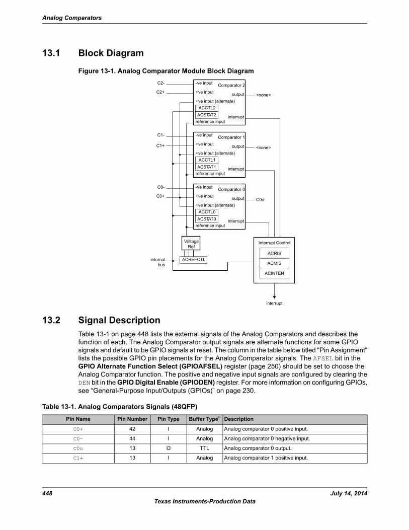
13.1 Block Diagram
Figure 13-1. Analog Comparator Module Block Diagram
C2+
C2-
output+ve input (alternate)
+ve input
interrupt
-ve input
reference input
Comparator 2
ACSTAT2ACCTL2
C1-
C1+ output+ve input (alternate)
+ve input
interrupt
-ve input
reference input
Comparator 1
ACSTAT1ACCTL1
<none>
VoltageRef
ACREFCTL
output+ve input (alternate)
+ve input
interrupt
-ve input
reference input
Comparator 0
ACSTAT0ACCTL0
C0+
internalbus
C0-
C0o
<none>
Interrupt Control
ACRIS
ACMIS
ACINTEN
interrupt
13.2 Signal DescriptionTable 13-1 on page 448 lists the external signals of the Analog Comparators and describes thefunction of each. The Analog Comparator output signals are alternate functions for some GPIOsignals and default to be GPIO signals at reset. The column in the table below titled "Pin Assignment"lists the possible GPIO pin placements for the Analog Comparator signals. The AFSEL bit in theGPIO Alternate Function Select (GPIOAFSEL) register (page 250) should be set to choose theAnalog Comparator function. The positive and negative input signals are configured by clearing theDEN bit in theGPIO Digital Enable (GPIODEN) register. For more information on configuring GPIOs,see “General-Purpose Input/Outputs (GPIOs)” on page 230.
Table 13-1. Analog Comparators Signals (48QFP)
DescriptionBuffer TypeaPin TypePin NumberPin Name
Analog comparator 0 positive input.AnalogI42C0+
Analog comparator 0 negative input.AnalogI44C0-
Analog comparator 0 output.TTLO13C0o
Analog comparator 1 positive input.AnalogI13C1+
July 14, 2014448Texas Instruments-Production Data
Analog Comparators
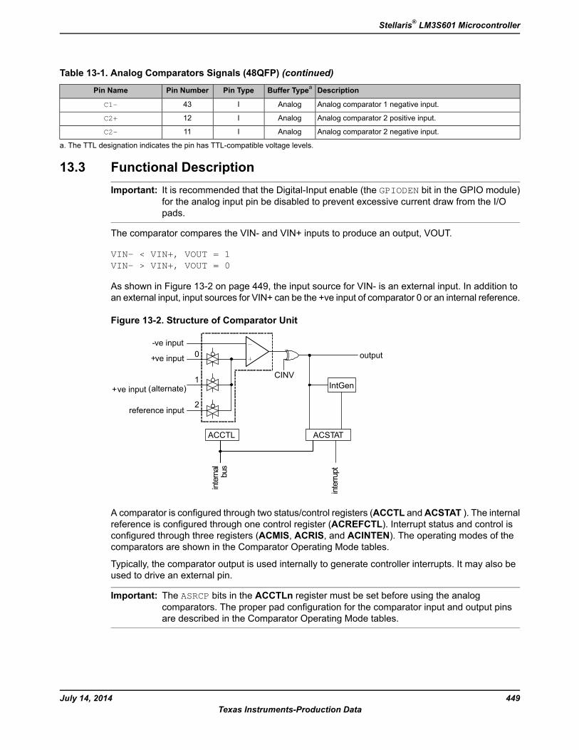
Table 13-1. Analog Comparators Signals (48QFP) (continued)
DescriptionBuffer TypeaPin TypePin NumberPin Name
Analog comparator 1 negative input.AnalogI43C1-
Analog comparator 2 positive input.AnalogI12C2+
Analog comparator 2 negative input.AnalogI11C2-
a. The TTL designation indicates the pin has TTL-compatible voltage levels.
13.3 Functional DescriptionImportant: It is recommended that the Digital-Input enable (the GPIODEN bit in the GPIO module)
for the analog input pin be disabled to prevent excessive current draw from the I/Opads.
The comparator compares the VIN- and VIN+ inputs to produce an output, VOUT.
VIN- < VIN+, VOUT = 1VIN- > VIN+, VOUT = 0
As shown in Figure 13-2 on page 449, the input source for VIN- is an external input. In addition toan external input, input sources for VIN+ can be the +ve input of comparator 0 or an internal reference.
Figure 13-2. Structure of Comparator Unit
output
reference input
ACCTL
IntGen
2
1
0
CINV
interrupt
internal
bus
ACSTAT
(alternate)+ve input
+ve input
-ve input
A comparator is configured through two status/control registers (ACCTL andACSTAT ). The internalreference is configured through one control register (ACREFCTL). Interrupt status and control isconfigured through three registers (ACMIS, ACRIS, and ACINTEN). The operating modes of thecomparators are shown in the Comparator Operating Mode tables.
Typically, the comparator output is used internally to generate controller interrupts. It may also beused to drive an external pin.
Important: The ASRCP bits in the ACCTLn register must be set before using the analogcomparators. The proper pad configuration for the comparator input and output pinsare described in the Comparator Operating Mode tables.
449July 14, 2014Texas Instruments-Production Data
Stellaris® LM3S601 Microcontroller
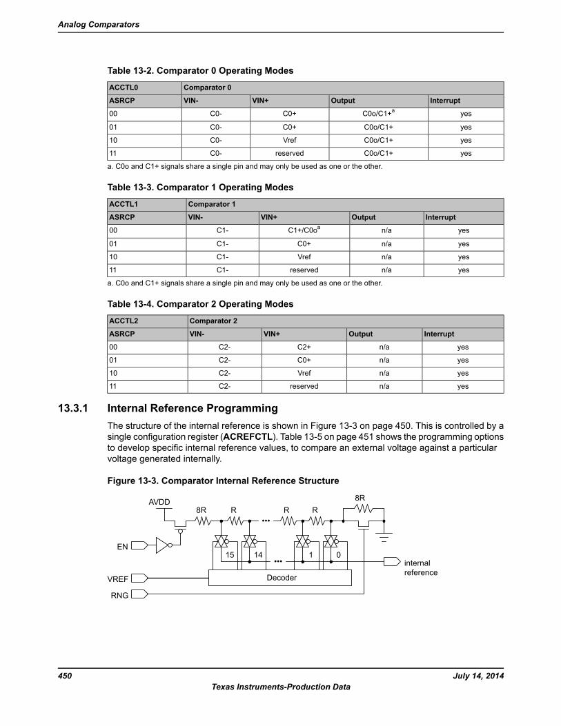
Table 13-2. Comparator 0 Operating Modes
Comparator 0ACCTL0
InterruptOutputVIN+VIN-ASRCP
yesC0o/C1+aC0+C0-00
yesC0o/C1+C0+C0-01
yesC0o/C1+VrefC0-10
yesC0o/C1+reservedC0-11
a. C0o and C1+ signals share a single pin and may only be used as one or the other.
Table 13-3. Comparator 1 Operating Modes
Comparator 1ACCTL1
InterruptOutputVIN+VIN-ASRCP
yesn/aC1+/C0oaC1-00
yesn/aC0+C1-01
yesn/aVrefC1-10
yesn/areservedC1-11
a. C0o and C1+ signals share a single pin and may only be used as one or the other.
Table 13-4. Comparator 2 Operating Modes
Comparator 2ACCTL2
InterruptOutputVIN+VIN-ASRCP
yesn/aC2+C2-00
yesn/aC0+C2-01
yesn/aVrefC2-10
yesn/areservedC2-11
13.3.1 Internal Reference ProgrammingThe structure of the internal reference is shown in Figure 13-3 on page 450. This is controlled by asingle configuration register (ACREFCTL). Table 13-5 on page 451 shows the programming optionsto develop specific internal reference values, to compare an external voltage against a particularvoltage generated internally.
Figure 13-3. Comparator Internal Reference Structure
8R R R8R
R•••
•••0
Decoder
115 14
AVDD
EN
internalreference
VREF
RNG
July 14, 2014450Texas Instruments-Production Data
Analog Comparators
Table 13-5. Internal Reference Voltage and ACREFCTL Field Values
Output Reference Voltage Based on VREF Field ValueACREFCTL Register
RNG Bit ValueEN Bit Value
0 V (GND) for any value of VREF; however, it is recommended that RNG=1 andVREF=0 for the least noisy ground reference.
RNG=XEN=0
Total resistance in ladder is 31 R.
The range of internal reference in this mode is 0.85-2.448 V.
RNG=0
EN=1Total resistance in ladder is 23 R.
The range of internal reference for this mode is 0-2.152 V.
RNG=1
13.4 Initialization and ConfigurationThe following example shows how to configure an analog comparator to read back its output valuefrom an internal register.
1. Enable the analog comparator 0 clock by writing a value of 0x0010.0000 to the RCGC1 registerin the System Control module.
2. In the GPIO module, enable the GPIO port/pin associated with C0- as a GPIO input.
3. Configure the internal voltage reference to 1.65 V by writing the ACREFCTL register with thevalue 0x0000.030C.
4. Configure comparator 0 to use the internal voltage reference and to not invert the output bywriting the ACCTL0 register with the value of 0x0000.040C.
5. Delay for some time.
6. Read the comparator output value by reading the ACSTAT0 register’s OVAL value.
Change the level of the signal input on C0- to see the OVAL value change.
13.5 Register MapTable 13-6 on page 452 lists the comparator registers. The offset listed is a hexadecimal incrementto the register’s address, relative to the Analog Comparator base address of 0x4003.C000.
451July 14, 2014Texas Instruments-Production Data
Stellaris® LM3S601 Microcontroller
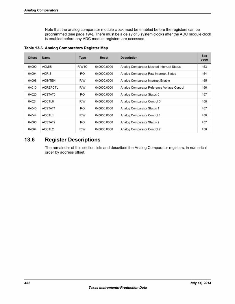
Note that the analog comparator module clock must be enabled before the registers can beprogrammed (see page 194). There must be a delay of 3 system clocks after the ADCmodule clockis enabled before any ADC module registers are accessed.
Table 13-6. Analog Comparators Register Map
SeepageDescriptionResetTypeNameOffset
453Analog Comparator Masked Interrupt Status0x0000.0000R/W1CACMIS0x000
454Analog Comparator Raw Interrupt Status0x0000.0000ROACRIS0x004
455Analog Comparator Interrupt Enable0x0000.0000R/WACINTEN0x008
456Analog Comparator Reference Voltage Control0x0000.0000R/WACREFCTL0x010
457Analog Comparator Status 00x0000.0000ROACSTAT00x020
458Analog Comparator Control 00x0000.0000R/WACCTL00x024
457Analog Comparator Status 10x0000.0000ROACSTAT10x040
458Analog Comparator Control 10x0000.0000R/WACCTL10x044
457Analog Comparator Status 20x0000.0000ROACSTAT20x060
458Analog Comparator Control 20x0000.0000R/WACCTL20x064
13.6 Register DescriptionsThe remainder of this section lists and describes the Analog Comparator registers, in numericalorder by address offset.
July 14, 2014452Texas Instruments-Production Data
Analog Comparators
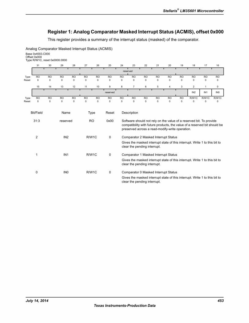
Register 1: Analog Comparator Masked Interrupt Status (ACMIS), offset 0x000This register provides a summary of the interrupt status (masked) of the comparator.
Analog Comparator Masked Interrupt Status (ACMIS)Base 0x4003.C000Offset 0x000Type R/W1C, reset 0x0000.0000
16171819202122232425262728293031
reserved
ROROROROROROROROROROROROROROROROType0000000000000000Reset
0123456789101112131415
IN0IN1IN2reserved
R/W1CR/W1CR/W1CROROROROROROROROROROROROROType0000000000000000Reset
DescriptionResetTypeNameBit/Field
Software should not rely on the value of a reserved bit. To providecompatibility with future products, the value of a reserved bit should bepreserved across a read-modify-write operation.
0x00ROreserved31:3
Comparator 2 Masked Interrupt StatusGives the masked interrupt state of this interrupt. Write 1 to this bit toclear the pending interrupt.
0R/W1CIN22
Comparator 1 Masked Interrupt StatusGives the masked interrupt state of this interrupt. Write 1 to this bit toclear the pending interrupt.
0R/W1CIN11
Comparator 0 Masked Interrupt StatusGives the masked interrupt state of this interrupt. Write 1 to this bit toclear the pending interrupt.
0R/W1CIN00
453July 14, 2014Texas Instruments-Production Data
Stellaris® LM3S601 Microcontroller
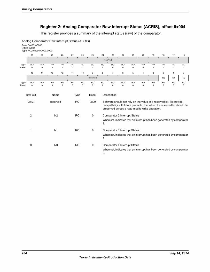
Register 2: Analog Comparator Raw Interrupt Status (ACRIS), offset 0x004This register provides a summary of the interrupt status (raw) of the comparator.
Analog Comparator Raw Interrupt Status (ACRIS)Base 0x4003.C000Offset 0x004Type RO, reset 0x0000.0000
16171819202122232425262728293031
reserved
ROROROROROROROROROROROROROROROROType0000000000000000Reset
0123456789101112131415
IN0IN1IN2reserved
ROROROROROROROROROROROROROROROROType0000000000000000Reset
DescriptionResetTypeNameBit/Field
Software should not rely on the value of a reserved bit. To providecompatibility with future products, the value of a reserved bit should bepreserved across a read-modify-write operation.
0x00ROreserved31:3
Comparator 2 Interrupt StatusWhen set, indicates that an interrupt has been generated by comparator2.
0ROIN22
Comparator 1 Interrupt StatusWhen set, indicates that an interrupt has been generated by comparator1.
0ROIN11
Comparator 0 Interrupt StatusWhen set, indicates that an interrupt has been generated by comparator0.
0ROIN00
July 14, 2014454Texas Instruments-Production Data
Analog Comparators
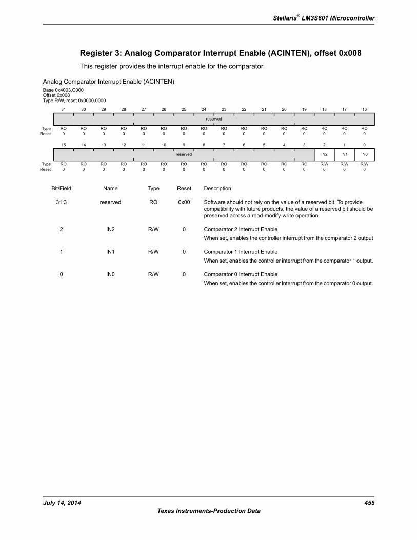
Register 3: Analog Comparator Interrupt Enable (ACINTEN), offset 0x008This register provides the interrupt enable for the comparator.
Analog Comparator Interrupt Enable (ACINTEN)Base 0x4003.C000Offset 0x008Type R/W, reset 0x0000.0000
16171819202122232425262728293031
reserved
ROROROROROROROROROROROROROROROROType0000000000000000Reset
0123456789101112131415
IN0IN1IN2reserved
R/WR/WR/WROROROROROROROROROROROROROType0000000000000000Reset
DescriptionResetTypeNameBit/Field
Software should not rely on the value of a reserved bit. To providecompatibility with future products, the value of a reserved bit should bepreserved across a read-modify-write operation.
0x00ROreserved31:3
Comparator 2 Interrupt EnableWhen set, enables the controller interrupt from the comparator 2 output
0R/WIN22
Comparator 1 Interrupt EnableWhen set, enables the controller interrupt from the comparator 1 output.
0R/WIN11
Comparator 0 Interrupt EnableWhen set, enables the controller interrupt from the comparator 0 output.
0R/WIN00
455July 14, 2014Texas Instruments-Production Data
Stellaris® LM3S601 Microcontroller
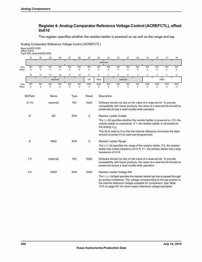
Register 4: Analog Comparator Reference Voltage Control (ACREFCTL), offset0x010This register specifies whether the resistor ladder is powered on as well as the range and tap.
Analog Comparator Reference Voltage Control (ACREFCTL)Base 0x4003.C000Offset 0x010Type R/W, reset 0x0000.0000
16171819202122232425262728293031
reserved
ROROROROROROROROROROROROROROROROType0000000000000000Reset
0123456789101112131415
VREFreservedRNGENreserved
R/WR/WR/WR/WROROROROR/WR/WROROROROROROType0000000000000000Reset
DescriptionResetTypeNameBit/Field
Software should not rely on the value of a reserved bit. To providecompatibility with future products, the value of a reserved bit should bepreserved across a read-modify-write operation.
0x00ROreserved31:10
Resistor Ladder EnableThe EN bit specifies whether the resistor ladder is powered on. If 0, theresistor ladder is unpowered. If 1, the resistor ladder is connected tothe analog VDD.
This bit is reset to 0 so that the internal reference consumes the leastamount of power if not used and programmed.
0R/WEN9
Resistor Ladder RangeThe RNG bit specifies the range of the resistor ladder. If 0, the resistorladder has a total resistance of 31 R. If 1, the resistor ladder has a totalresistance of 23 R.
0R/WRNG8
Software should not rely on the value of a reserved bit. To providecompatibility with future products, the value of a reserved bit should bepreserved across a read-modify-write operation.
0x00ROreserved7:4
Resistor Ladder Voltage RefThe VREF bit field specifies the resistor ladder tap that is passed throughan analog multiplexer. The voltage corresponding to the tap position isthe internal reference voltage available for comparison. See Table13-5 on page 451 for some output reference voltage examples.
0x00R/WVREF3:0
July 14, 2014456Texas Instruments-Production Data
Analog Comparators
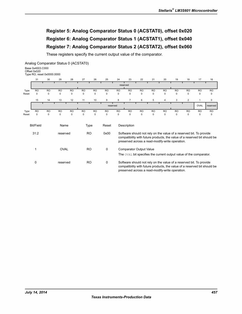
Register 5: Analog Comparator Status 0 (ACSTAT0), offset 0x020Register 6: Analog Comparator Status 1 (ACSTAT1), offset 0x040Register 7: Analog Comparator Status 2 (ACSTAT2), offset 0x060These registers specify the current output value of the comparator.
Analog Comparator Status 0 (ACSTAT0)Base 0x4003.C000Offset 0x020Type RO, reset 0x0000.0000
16171819202122232425262728293031
reserved
ROROROROROROROROROROROROROROROROType0000000000000000Reset
0123456789101112131415
reservedOVALreserved
ROROROROROROROROROROROROROROROROType0000000000000000Reset
DescriptionResetTypeNameBit/Field
Software should not rely on the value of a reserved bit. To providecompatibility with future products, the value of a reserved bit should bepreserved across a read-modify-write operation.
0x00ROreserved31:2
Comparator Output ValueThe OVAL bit specifies the current output value of the comparator.
0ROOVAL1
Software should not rely on the value of a reserved bit. To providecompatibility with future products, the value of a reserved bit should bepreserved across a read-modify-write operation.
0ROreserved0
457July 14, 2014Texas Instruments-Production Data
Stellaris® LM3S601 Microcontroller
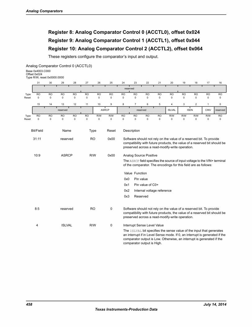
Register 8: Analog Comparator Control 0 (ACCTL0), offset 0x024Register 9: Analog Comparator Control 1 (ACCTL1), offset 0x044Register 10: Analog Comparator Control 2 (ACCTL2), offset 0x064These registers configure the comparator’s input and output.
Analog Comparator Control 0 (ACCTL0)Base 0x4003.C000Offset 0x024Type R/W, reset 0x0000.0000
16171819202122232425262728293031
reserved
ROROROROROROROROROROROROROROROROType0000000000000000Reset
0123456789101112131415
reservedCINVISENISLVALreservedASRCPreserved
ROR/WR/WR/WR/WROROROROR/WR/WROROROROROType0000000000000000Reset
DescriptionResetTypeNameBit/Field
Software should not rely on the value of a reserved bit. To providecompatibility with future products, the value of a reserved bit should bepreserved across a read-modify-write operation.
0x00ROreserved31:11
Analog Source PositiveThe ASRCP field specifies the source of input voltage to the VIN+ terminalof the comparator. The encodings for this field are as follows:
FunctionValue
Pin value0x0
Pin value of C0+0x1
Internal voltage reference0x2
Reserved0x3
0x00R/WASRCP10:9
Software should not rely on the value of a reserved bit. To providecompatibility with future products, the value of a reserved bit should bepreserved across a read-modify-write operation.
0ROreserved8:5
Interrupt Sense Level ValueThe ISLVAL bit specifies the sense value of the input that generatesan interrupt if in Level Sense mode. If 0, an interrupt is generated if thecomparator output is Low. Otherwise, an interrupt is generated if thecomparator output is High.
0R/WISLVAL4
July 14, 2014458Texas Instruments-Production Data
Analog Comparators
DescriptionResetTypeNameBit/Field
Interrupt SenseThe ISEN field specifies the sense of the comparator output thatgenerates an interrupt. The sense conditioning is as follows:
FunctionValue
Level sense, see ISLVAL0x0
Falling edge0x1
Rising edge0x2
Either edge0x3
0x0R/WISEN3:2
Comparator Output InvertThe CINV bit conditionally inverts the output of the comparator. If 0, theoutput of the comparator is unchanged. If 1, the output of the comparatoris inverted prior to being processed by hardware.
0R/WCINV1
Software should not rely on the value of a reserved bit. To providecompatibility with future products, the value of a reserved bit should bepreserved across a read-modify-write operation.
0ROreserved0
459July 14, 2014Texas Instruments-Production Data
Stellaris® LM3S601 Microcontroller
14 Pulse Width Modulator (PWM)Pulse width modulation (PWM) is a powerful technique for digitally encoding analog signal levels.High-resolution counters are used to generate a square wave, and the duty cycle of the squarewave is modulated to encode an analog signal. Typical applications include switching power suppliesand motor control.
The Stellaris® PWMmodule consists of three PWM generator blocks and a control block. The controlblock determines the polarity of the PWM signals, and which signals are passed through to the pins.
Each PWM generator block produces two PWM signals that can either be independent signals(other than being based on the same timer and therefore having the same frequency) or a singlepair of complementary signals with dead-band delays inserted. The output of the PWM generationblocks are managed by the output control block before being passed to the device pins.
The Stellaris PWM module provides a great deal of flexibility. It can generate simple PWM signals,such as those required by a simple charge pump. It can also generate paired PWM signals withdead-band delays, such as those required by a half-H bridge driver. Three generator blocks canalso generate the full six channels of gate controls required by a 3-phase inverter bridge.
Each Stellaris PWM module has the following features:
Three PWM generator blocks, each with one 16-bit counter, two PWM comparators, a PWMsignal generator, a dead-band generator, and an interrupt selector
One fault input in hardware to promote low-latency shutdown
One 16-bit counter
– Runs in Down or Up/Down mode
– Output frequency controlled by a 16-bit load value
– Load value updates can be synchronized
– Produces output signals at zero and load value
Two PWM comparators
– Comparator value updates can be synchronized
– Produces output signals on match
PWM generator
– Output PWM signal is constructed based on actions taken as a result of the counter andPWM comparator output signals
– Produces two independent PWM signals
Dead-band generator
– Produces two PWM signals with programmable dead-band delays suitable for driving a half-Hbridge
– Can be bypassed, leaving input PWM signals unmodified
July 14, 2014460Texas Instruments-Production Data
Pulse Width Modulator (PWM)
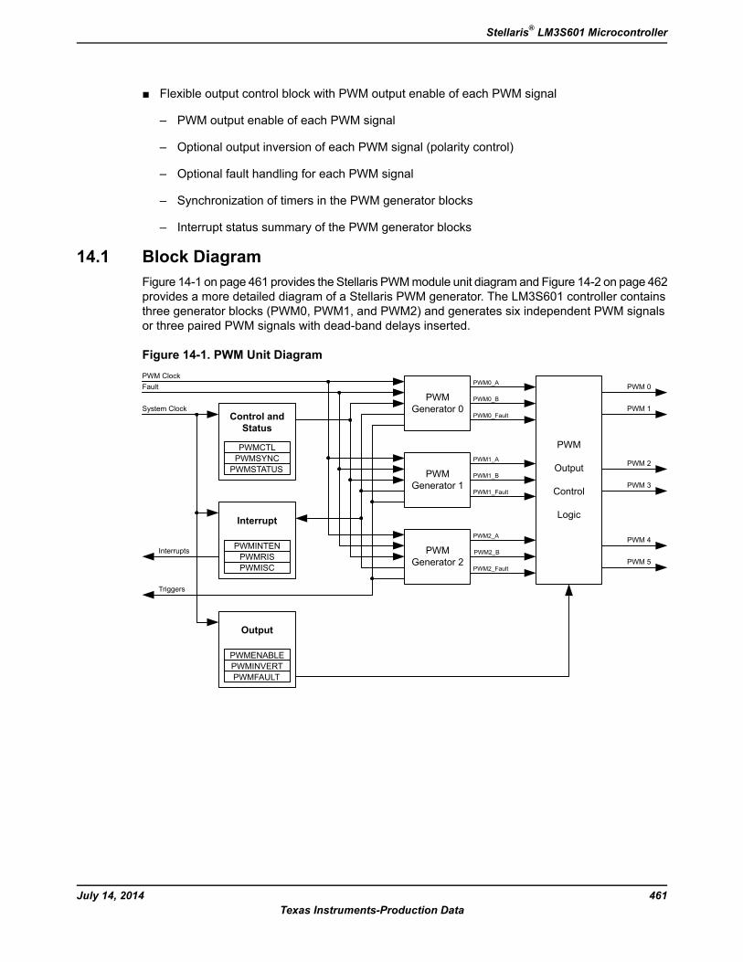
Flexible output control block with PWM output enable of each PWM signal
– PWM output enable of each PWM signal
– Optional output inversion of each PWM signal (polarity control)
– Optional fault handling for each PWM signal
– Synchronization of timers in the PWM generator blocks
– Interrupt status summary of the PWM generator blocks
14.1 Block DiagramFigure 14-1 on page 461 provides the Stellaris PWMmodule unit diagram and Figure 14-2 on page 462provides a more detailed diagram of a Stellaris PWM generator. The LM3S601 controller containsthree generator blocks (PWM0, PWM1, and PWM2) and generates six independent PWM signalsor three paired PWM signals with dead-band delays inserted.
Figure 14-1. PWM Unit Diagram
PWMINTEN
Interrupt
PWMRISPWMISC
PWMCTL
Control andStatus
PWMSYNCPWMSTATUS
PWMGenerator 0
PWMGenerator 1
PWMGenerator 2
PWM 0
PWM 1
PWM 2
PWM 3
PWM 4
PWM 5
PWM
Output
Control
Logic
PWM Clock
System Clock
Interrupts
Triggers
PWM0_A
PWM0_B
PWM1_A
PWM1_B
PWM2_A
PWM2_B
PWM0_Fault
PWM1_Fault
PWM2_Fault
Fault
PWMENABLE
Output
PWMINVERTPWMFAULT
461July 14, 2014Texas Instruments-Production Data
Stellaris® LM3S601 Microcontroller
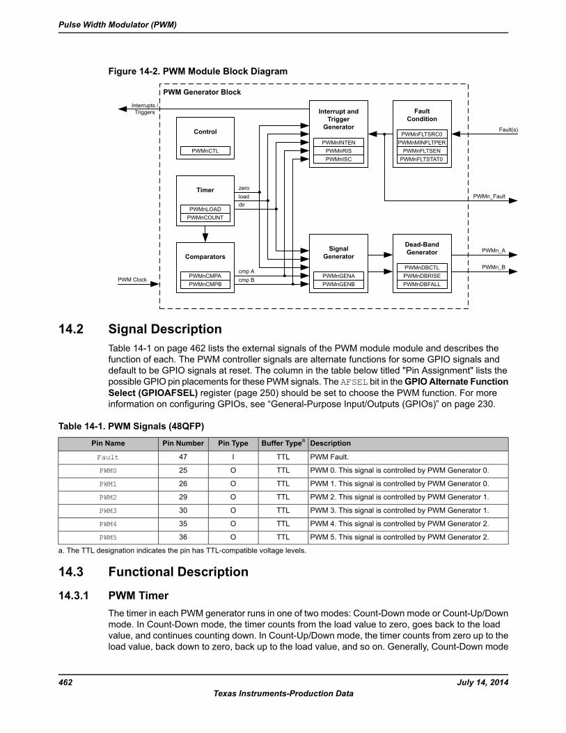
Figure 14-2. PWM Module Block Diagram
PWMnCMPA
Comparators
PWMnCMPB
PWMnLOAD
Timer
PWMnCOUNT
PWMnDBCTL
Dead-BandGenerator
PWMnDBRISEPWMnDBFALL
PWMnCTL
Control
PWM Clock
PWM Generator Block
SignalGenerator
PWMnGENAPWMnGENB
PWMnINTEN
Interrupt andTrigger
Generator
PWMnRISPWMnISC
Fault(s)
PWMn_A
PWMn_B
Interrupts /Triggers
PWMn_Fault
cmp Acmp B
zeroloaddir
PWMnFLTSRC0
FaultCondition
PWMnMINFLTPERPWMnFLTSENPWMnFLTSTAT0
14.2 Signal DescriptionTable 14-1 on page 462 lists the external signals of the PWM module module and describes thefunction of each. The PWM controller signals are alternate functions for some GPIO signals anddefault to be GPIO signals at reset. The column in the table below titled "Pin Assignment" lists thepossible GPIO pin placements for these PWMsignals. The AFSEL bit in theGPIOAlternate FunctionSelect (GPIOAFSEL) register (page 250) should be set to choose the PWM function. For moreinformation on configuring GPIOs, see “General-Purpose Input/Outputs (GPIOs)” on page 230.
Table 14-1. PWM Signals (48QFP)
DescriptionBuffer TypeaPin TypePin NumberPin Name
PWM Fault.TTLI47Fault
PWM 0. This signal is controlled by PWM Generator 0.TTLO25PWM0
PWM 1. This signal is controlled by PWM Generator 0.TTLO26PWM1
PWM 2. This signal is controlled by PWM Generator 1.TTLO29PWM2
PWM 3. This signal is controlled by PWM Generator 1.TTLO30PWM3
PWM 4. This signal is controlled by PWM Generator 2.TTLO35PWM4
PWM 5. This signal is controlled by PWM Generator 2.TTLO36PWM5
a. The TTL designation indicates the pin has TTL-compatible voltage levels.
14.3 Functional Description
14.3.1 PWM TimerThe timer in each PWM generator runs in one of two modes: Count-Down mode or Count-Up/Downmode. In Count-Down mode, the timer counts from the load value to zero, goes back to the loadvalue, and continues counting down. In Count-Up/Down mode, the timer counts from zero up to theload value, back down to zero, back up to the load value, and so on. Generally, Count-Down mode
July 14, 2014462Texas Instruments-Production Data
Pulse Width Modulator (PWM)
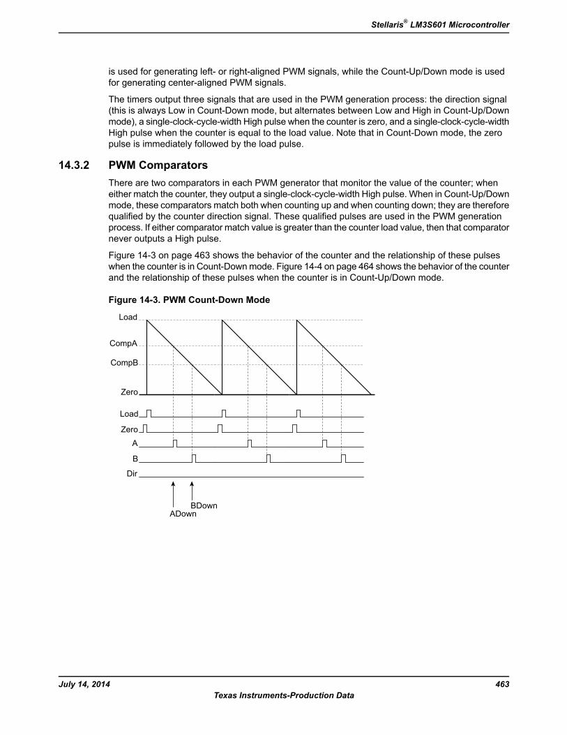
is used for generating left- or right-aligned PWM signals, while the Count-Up/Down mode is usedfor generating center-aligned PWM signals.
The timers output three signals that are used in the PWM generation process: the direction signal(this is always Low in Count-Down mode, but alternates between Low and High in Count-Up/Downmode), a single-clock-cycle-width High pulse when the counter is zero, and a single-clock-cycle-widthHigh pulse when the counter is equal to the load value. Note that in Count-Down mode, the zeropulse is immediately followed by the load pulse.
14.3.2 PWM ComparatorsThere are two comparators in each PWM generator that monitor the value of the counter; wheneither match the counter, they output a single-clock-cycle-width High pulse. When in Count-Up/Downmode, these comparators match both when counting up and when counting down; they are thereforequalified by the counter direction signal. These qualified pulses are used in the PWM generationprocess. If either comparator match value is greater than the counter load value, then that comparatornever outputs a High pulse.
Figure 14-3 on page 463 shows the behavior of the counter and the relationship of these pulseswhen the counter is in Count-Downmode. Figure 14-4 on page 464 shows the behavior of the counterand the relationship of these pulses when the counter is in Count-Up/Down mode.
Figure 14-3. PWM Count-Down Mode
Load
Zero
CompB
CompA
Load
Zero
B
A
Dir
ADownBDown
463July 14, 2014Texas Instruments-Production Data
Stellaris® LM3S601 Microcontroller
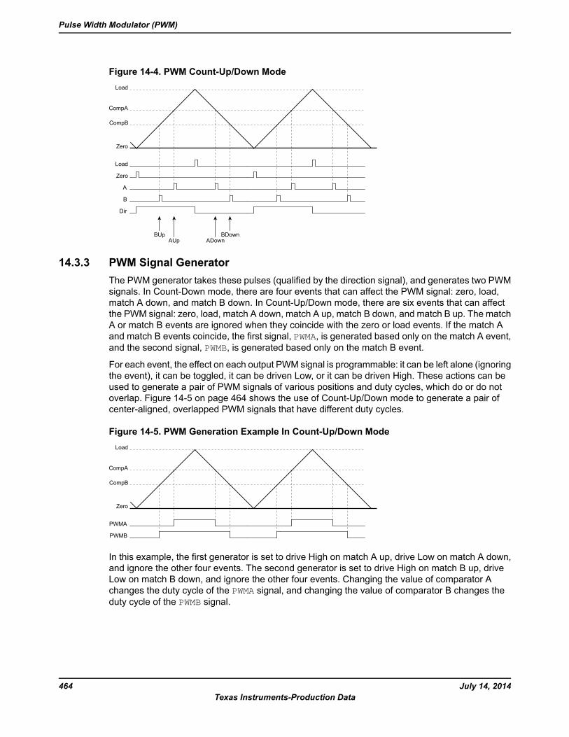
Figure 14-4. PWM Count-Up/Down ModeLoad
Zero
CompB
CompA
Load
Zero
B
A
Dir
BUpAUp ADown
BDown
14.3.3 PWM Signal GeneratorThe PWM generator takes these pulses (qualified by the direction signal), and generates two PWMsignals. In Count-Down mode, there are four events that can affect the PWM signal: zero, load,match A down, and match B down. In Count-Up/Down mode, there are six events that can affectthe PWM signal: zero, load, match A down, match A up, match B down, and match B up. The matchA or match B events are ignored when they coincide with the zero or load events. If the match Aand match B events coincide, the first signal, PWMA, is generated based only on the match A event,and the second signal, PWMB, is generated based only on the match B event.
For each event, the effect on each output PWM signal is programmable: it can be left alone (ignoringthe event), it can be toggled, it can be driven Low, or it can be driven High. These actions can beused to generate a pair of PWM signals of various positions and duty cycles, which do or do notoverlap. Figure 14-5 on page 464 shows the use of Count-Up/Down mode to generate a pair ofcenter-aligned, overlapped PWM signals that have different duty cycles.
Figure 14-5. PWM Generation Example In Count-Up/Down ModeLoad
Zero
CompB
CompA
PWMB
PWMA
In this example, the first generator is set to drive High on match A up, drive Low on match A down,and ignore the other four events. The second generator is set to drive High on match B up, driveLow on match B down, and ignore the other four events. Changing the value of comparator Achanges the duty cycle of the PWMA signal, and changing the value of comparator B changes theduty cycle of the PWMB signal.
July 14, 2014464Texas Instruments-Production Data
Pulse Width Modulator (PWM)
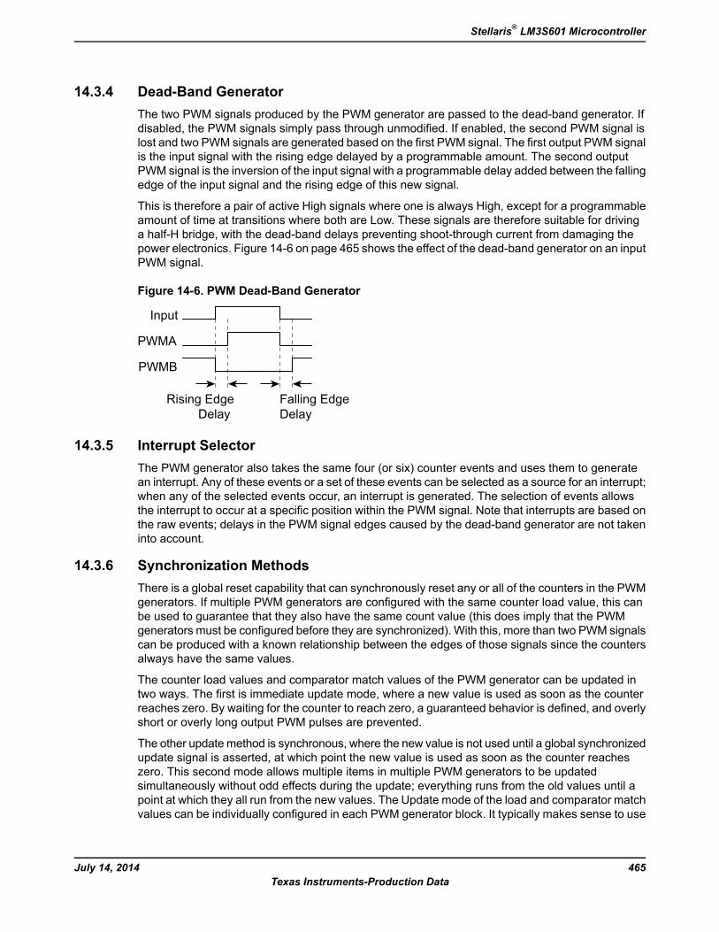
14.3.4 Dead-Band GeneratorThe two PWM signals produced by the PWM generator are passed to the dead-band generator. Ifdisabled, the PWM signals simply pass through unmodified. If enabled, the second PWM signal islost and two PWM signals are generated based on the first PWM signal. The first output PWM signalis the input signal with the rising edge delayed by a programmable amount. The second outputPWM signal is the inversion of the input signal with a programmable delay added between the fallingedge of the input signal and the rising edge of this new signal.
This is therefore a pair of active High signals where one is always High, except for a programmableamount of time at transitions where both are Low. These signals are therefore suitable for drivinga half-H bridge, with the dead-band delays preventing shoot-through current from damaging thepower electronics. Figure 14-6 on page 465 shows the effect of the dead-band generator on an inputPWM signal.
Figure 14-6. PWM Dead-Band Generator
Input
PWMA
PWMB
Rising EdgeDelay
Falling EdgeDelay
14.3.5 Interrupt SelectorThe PWM generator also takes the same four (or six) counter events and uses them to generatean interrupt. Any of these events or a set of these events can be selected as a source for an interrupt;when any of the selected events occur, an interrupt is generated. The selection of events allowsthe interrupt to occur at a specific position within the PWM signal. Note that interrupts are based onthe raw events; delays in the PWM signal edges caused by the dead-band generator are not takeninto account.
14.3.6 Synchronization MethodsThere is a global reset capability that can synchronously reset any or all of the counters in the PWMgenerators. If multiple PWM generators are configured with the same counter load value, this canbe used to guarantee that they also have the same count value (this does imply that the PWMgenerators must be configured before they are synchronized). With this, more than two PWM signalscan be produced with a known relationship between the edges of those signals since the countersalways have the same values.
The counter load values and comparator match values of the PWM generator can be updated intwo ways. The first is immediate update mode, where a new value is used as soon as the counterreaches zero. By waiting for the counter to reach zero, a guaranteed behavior is defined, and overlyshort or overly long output PWM pulses are prevented.
The other update method is synchronous, where the new value is not used until a global synchronizedupdate signal is asserted, at which point the new value is used as soon as the counter reacheszero. This second mode allows multiple items in multiple PWM generators to be updatedsimultaneously without odd effects during the update; everything runs from the old values until apoint at which they all run from the new values. The Update mode of the load and comparator matchvalues can be individually configured in each PWM generator block. It typically makes sense to use
465July 14, 2014Texas Instruments-Production Data
Stellaris® LM3S601 Microcontroller
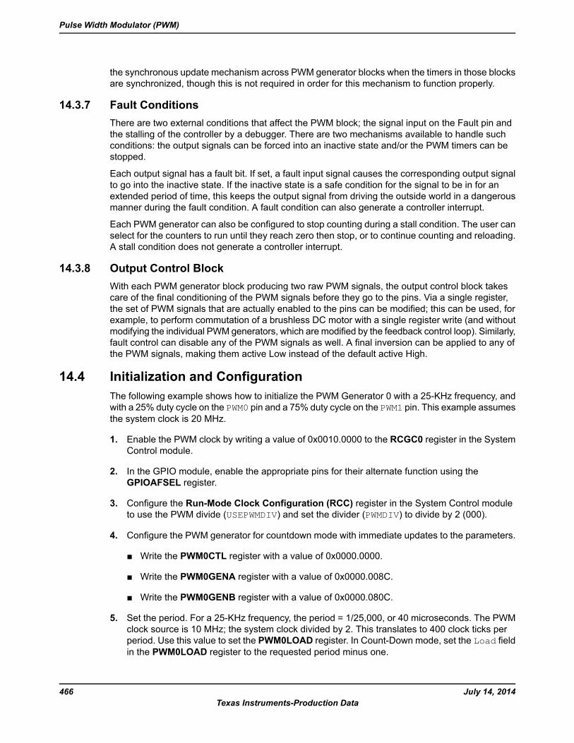
the synchronous update mechanism across PWM generator blocks when the timers in those blocksare synchronized, though this is not required in order for this mechanism to function properly.
14.3.7 Fault ConditionsThere are two external conditions that affect the PWM block; the signal input on the Fault pin andthe stalling of the controller by a debugger. There are two mechanisms available to handle suchconditions: the output signals can be forced into an inactive state and/or the PWM timers can bestopped.
Each output signal has a fault bit. If set, a fault input signal causes the corresponding output signalto go into the inactive state. If the inactive state is a safe condition for the signal to be in for anextended period of time, this keeps the output signal from driving the outside world in a dangerousmanner during the fault condition. A fault condition can also generate a controller interrupt.
Each PWM generator can also be configured to stop counting during a stall condition. The user canselect for the counters to run until they reach zero then stop, or to continue counting and reloading.A stall condition does not generate a controller interrupt.
14.3.8 Output Control BlockWith each PWM generator block producing two raw PWM signals, the output control block takescare of the final conditioning of the PWM signals before they go to the pins. Via a single register,the set of PWM signals that are actually enabled to the pins can be modified; this can be used, forexample, to perform commutation of a brushless DC motor with a single register write (and withoutmodifying the individual PWM generators, which are modified by the feedback control loop). Similarly,fault control can disable any of the PWM signals as well. A final inversion can be applied to any ofthe PWM signals, making them active Low instead of the default active High.
14.4 Initialization and ConfigurationThe following example shows how to initialize the PWM Generator 0 with a 25-KHz frequency, andwith a 25% duty cycle on the PWM0 pin and a 75% duty cycle on the PWM1 pin. This example assumesthe system clock is 20 MHz.
1. Enable the PWM clock by writing a value of 0x0010.0000 to the RCGC0 register in the SystemControl module.
2. In the GPIO module, enable the appropriate pins for their alternate function using theGPIOAFSEL register.
3. Configure the Run-Mode Clock Configuration (RCC) register in the System Control moduleto use the PWM divide (USEPWMDIV) and set the divider (PWMDIV) to divide by 2 (000).
4. Configure the PWM generator for countdown mode with immediate updates to the parameters.
Write the PWM0CTL register with a value of 0x0000.0000.
Write the PWM0GENA register with a value of 0x0000.008C.
Write the PWM0GENB register with a value of 0x0000.080C.
5. Set the period. For a 25-KHz frequency, the period = 1/25,000, or 40 microseconds. The PWMclock source is 10 MHz; the system clock divided by 2. This translates to 400 clock ticks perperiod. Use this value to set the PWM0LOAD register. In Count-Down mode, set the Load fieldin the PWM0LOAD register to the requested period minus one.
July 14, 2014466Texas Instruments-Production Data
Pulse Width Modulator (PWM)
Write the PWM0LOAD register with a value of 0x0000.018F.
6. Set the pulse width of the PWM0 pin for a 25% duty cycle.
Write the PWM0CMPA register with a value of 0x0000.012B.
7. Set the pulse width of the PWM1 pin for a 75% duty cycle.
Write the PWM0CMPB register with a value of 0x0000.0063.
8. Start the timers in PWM generator 0.
Write the PWM0CTL register with a value of 0x0000.0001.
9. Enable PWM outputs.
Write the PWMENABLE register with a value of 0x0000.0003.
14.5 Register MapTable 14-2 on page 467 lists the PWM registers. The offset listed is a hexadecimal increment to theregister’s address, relative to the PWM base address of 0x4002.8000. Note that the PWM moduleclock must be enabled before the registers can be programmed (see page 191). There must be adelay of 3 system clocks after the PWMmodule clock is enabled before any PWMmodule registersare accessed.
Table 14-2. PWM Register Map
SeepageDescriptionResetTypeNameOffset
470PWM Master Control0x0000.0000R/WPWMCTL0x000
471PWM Time Base Sync0x0000.0000R/WPWMSYNC0x004
472PWM Output Enable0x0000.0000R/WPWMENABLE0x008
473PWM Output Inversion0x0000.0000R/WPWMINVERT0x00C
474PWM Output Fault0x0000.0000R/WPWMFAULT0x010
475PWM Interrupt Enable0x0000.0000R/WPWMINTEN0x014
476PWM Raw Interrupt Status0x0000.0000ROPWMRIS0x018
477PWM Interrupt Status and Clear0x0000.0000R/W1CPWMISC0x01C
478PWM Status0x0000.0000ROPWMSTATUS0x020
479PWM0 Control0x0000.0000R/WPWM0CTL0x040
481PWM0 Interrupt Enable0x0000.0000R/WPWM0INTEN0x044
483PWM0 Raw Interrupt Status0x0000.0000ROPWM0RIS0x048
484PWM0 Interrupt Status and Clear0x0000.0000R/W1CPWM0ISC0x04C
485PWM0 Load0x0000.0000R/WPWM0LOAD0x050
486PWM0 Counter0x0000.0000ROPWM0COUNT0x054
487PWM0 Compare A0x0000.0000R/WPWM0CMPA0x058
467July 14, 2014Texas Instruments-Production Data
Stellaris® LM3S601 Microcontroller
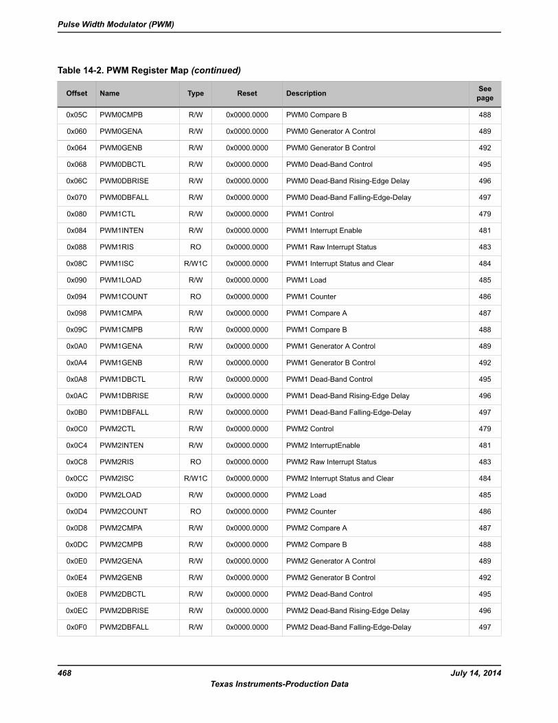
Table 14-2. PWM Register Map (continued)
SeepageDescriptionResetTypeNameOffset
488PWM0 Compare B0x0000.0000R/WPWM0CMPB0x05C
489PWM0 Generator A Control0x0000.0000R/WPWM0GENA0x060
492PWM0 Generator B Control0x0000.0000R/WPWM0GENB0x064
495PWM0 Dead-Band Control0x0000.0000R/WPWM0DBCTL0x068
496PWM0 Dead-Band Rising-Edge Delay0x0000.0000R/WPWM0DBRISE0x06C
497PWM0 Dead-Band Falling-Edge-Delay0x0000.0000R/WPWM0DBFALL0x070
479PWM1 Control0x0000.0000R/WPWM1CTL0x080
481PWM1 Interrupt Enable0x0000.0000R/WPWM1INTEN0x084
483PWM1 Raw Interrupt Status0x0000.0000ROPWM1RIS0x088
484PWM1 Interrupt Status and Clear0x0000.0000R/W1CPWM1ISC0x08C
485PWM1 Load0x0000.0000R/WPWM1LOAD0x090
486PWM1 Counter0x0000.0000ROPWM1COUNT0x094
487PWM1 Compare A0x0000.0000R/WPWM1CMPA0x098
488PWM1 Compare B0x0000.0000R/WPWM1CMPB0x09C
489PWM1 Generator A Control0x0000.0000R/WPWM1GENA0x0A0
492PWM1 Generator B Control0x0000.0000R/WPWM1GENB0x0A4
495PWM1 Dead-Band Control0x0000.0000R/WPWM1DBCTL0x0A8
496PWM1 Dead-Band Rising-Edge Delay0x0000.0000R/WPWM1DBRISE0x0AC
497PWM1 Dead-Band Falling-Edge-Delay0x0000.0000R/WPWM1DBFALL0x0B0
479PWM2 Control0x0000.0000R/WPWM2CTL0x0C0
481PWM2 InterruptEnable0x0000.0000R/WPWM2INTEN0x0C4
483PWM2 Raw Interrupt Status0x0000.0000ROPWM2RIS0x0C8
484PWM2 Interrupt Status and Clear0x0000.0000R/W1CPWM2ISC0x0CC
485PWM2 Load0x0000.0000R/WPWM2LOAD0x0D0
486PWM2 Counter0x0000.0000ROPWM2COUNT0x0D4
487PWM2 Compare A0x0000.0000R/WPWM2CMPA0x0D8
488PWM2 Compare B0x0000.0000R/WPWM2CMPB0x0DC
489PWM2 Generator A Control0x0000.0000R/WPWM2GENA0x0E0
492PWM2 Generator B Control0x0000.0000R/WPWM2GENB0x0E4
495PWM2 Dead-Band Control0x0000.0000R/WPWM2DBCTL0x0E8
496PWM2 Dead-Band Rising-Edge Delay0x0000.0000R/WPWM2DBRISE0x0EC
497PWM2 Dead-Band Falling-Edge-Delay0x0000.0000R/WPWM2DBFALL0x0F0
July 14, 2014468Texas Instruments-Production Data
Pulse Width Modulator (PWM)
14.6 Register DescriptionsThe remainder of this section lists and describes the PWM registers, in numerical order by addressoffset.
469July 14, 2014Texas Instruments-Production Data
Stellaris® LM3S601 Microcontroller
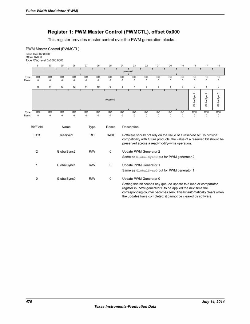
Register 1: PWM Master Control (PWMCTL), offset 0x000This register provides master control over the PWM generation blocks.
PWM Master Control (PWMCTL)Base 0x4002.8000Offset 0x000Type R/W, reset 0x0000.0000
16171819202122232425262728293031
reserved
ROROROROROROROROROROROROROROROROType0000000000000000Reset
0123456789101112131415
GlobalSync0
GlobalSync1
GlobalSync2
reserved
R/WR/WR/WROROROROROROROROROROROROROType0000000000000000Reset
DescriptionResetTypeNameBit/Field
Software should not rely on the value of a reserved bit. To providecompatibility with future products, the value of a reserved bit should bepreserved across a read-modify-write operation.
0x00ROreserved31:3
Update PWM Generator 2Same as GlobalSync0 but for PWM generator 2.
0R/WGlobalSync22
Update PWM Generator 1Same as GlobalSync0 but for PWM generator 1.
0R/WGlobalSync11
Update PWM Generator 0Setting this bit causes any queued update to a load or comparatorregister in PWM generator 0 to be applied the next time thecorresponding counter becomes zero. This bit automatically clears whenthe updates have completed; it cannot be cleared by software.
0R/WGlobalSync00
July 14, 2014470Texas Instruments-Production Data
Pulse Width Modulator (PWM)
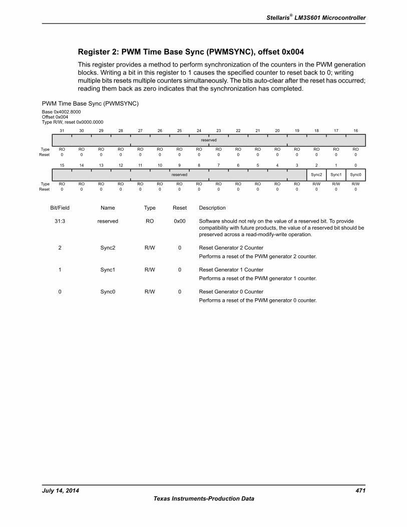
Register 2: PWM Time Base Sync (PWMSYNC), offset 0x004This register provides a method to perform synchronization of the counters in the PWM generationblocks. Writing a bit in this register to 1 causes the specified counter to reset back to 0; writingmultiple bits resets multiple counters simultaneously. The bits auto-clear after the reset has occurred;reading them back as zero indicates that the synchronization has completed.
PWM Time Base Sync (PWMSYNC)Base 0x4002.8000Offset 0x004Type R/W, reset 0x0000.0000
16171819202122232425262728293031
reserved
ROROROROROROROROROROROROROROROROType0000000000000000Reset
0123456789101112131415
Sync0Sync1Sync2reserved
R/WR/WR/WROROROROROROROROROROROROROType0000000000000000Reset
DescriptionResetTypeNameBit/Field
Software should not rely on the value of a reserved bit. To providecompatibility with future products, the value of a reserved bit should bepreserved across a read-modify-write operation.
0x00ROreserved31:3
Reset Generator 2 CounterPerforms a reset of the PWM generator 2 counter.
0R/WSync22
Reset Generator 1 CounterPerforms a reset of the PWM generator 1 counter.
0R/WSync11
Reset Generator 0 CounterPerforms a reset of the PWM generator 0 counter.
0R/WSync00
471July 14, 2014Texas Instruments-Production Data
Stellaris® LM3S601 Microcontroller
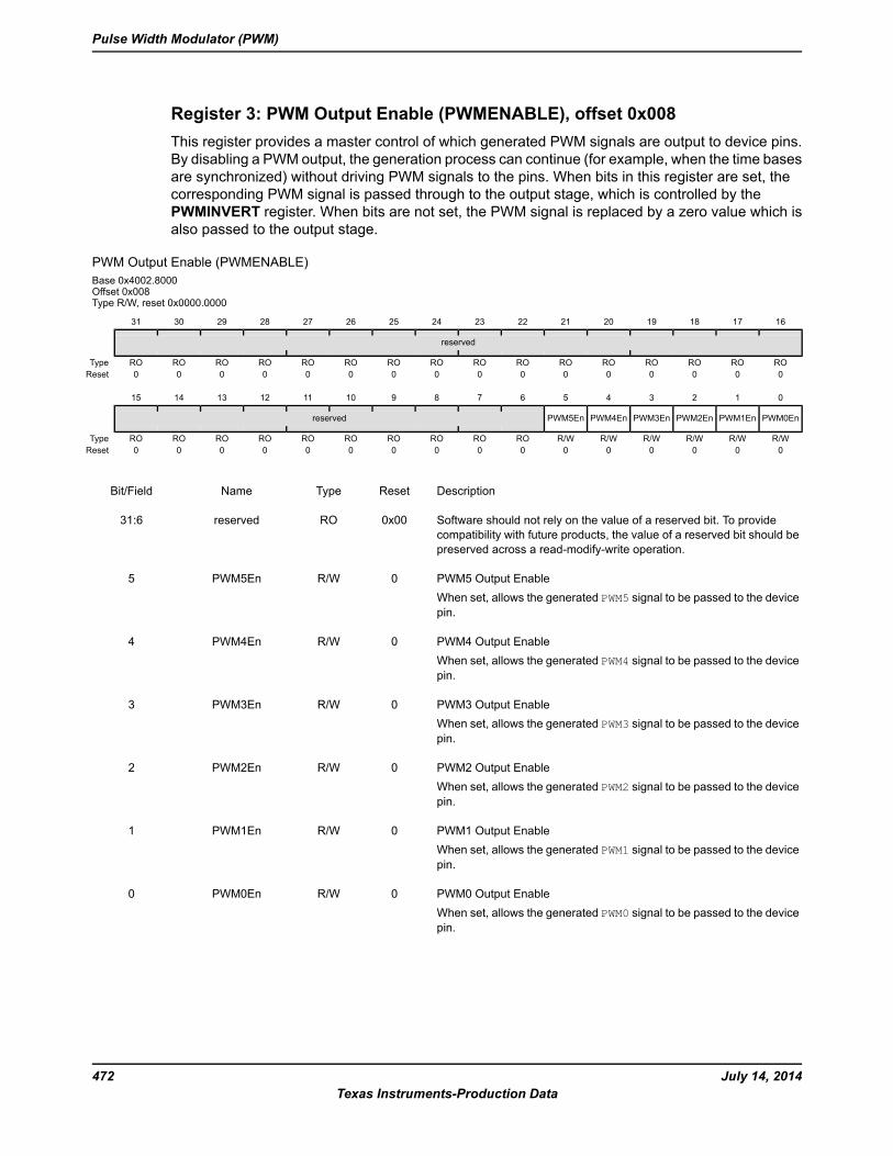
Register 3: PWM Output Enable (PWMENABLE), offset 0x008This register provides a master control of which generated PWM signals are output to device pins.By disabling a PWM output, the generation process can continue (for example, when the time basesare synchronized) without driving PWM signals to the pins. When bits in this register are set, thecorresponding PWM signal is passed through to the output stage, which is controlled by thePWMINVERT register. When bits are not set, the PWM signal is replaced by a zero value which isalso passed to the output stage.
PWM Output Enable (PWMENABLE)Base 0x4002.8000Offset 0x008Type R/W, reset 0x0000.0000
16171819202122232425262728293031
reserved
ROROROROROROROROROROROROROROROROType0000000000000000Reset
0123456789101112131415
PWM0EnPWM1EnPWM2EnPWM3EnPWM4EnPWM5Enreserved
R/WR/WR/WR/WR/WR/WROROROROROROROROROROType0000000000000000Reset
DescriptionResetTypeNameBit/Field
Software should not rely on the value of a reserved bit. To providecompatibility with future products, the value of a reserved bit should bepreserved across a read-modify-write operation.
0x00ROreserved31:6
PWM5 Output EnableWhen set, allows the generated PWM5 signal to be passed to the devicepin.
0R/WPWM5En5
PWM4 Output EnableWhen set, allows the generated PWM4 signal to be passed to the devicepin.
0R/WPWM4En4
PWM3 Output EnableWhen set, allows the generated PWM3 signal to be passed to the devicepin.
0R/WPWM3En3
PWM2 Output EnableWhen set, allows the generated PWM2 signal to be passed to the devicepin.
0R/WPWM2En2
PWM1 Output EnableWhen set, allows the generated PWM1 signal to be passed to the devicepin.
0R/WPWM1En1
PWM0 Output EnableWhen set, allows the generated PWM0 signal to be passed to the devicepin.
0R/WPWM0En0
July 14, 2014472Texas Instruments-Production Data
Pulse Width Modulator (PWM)
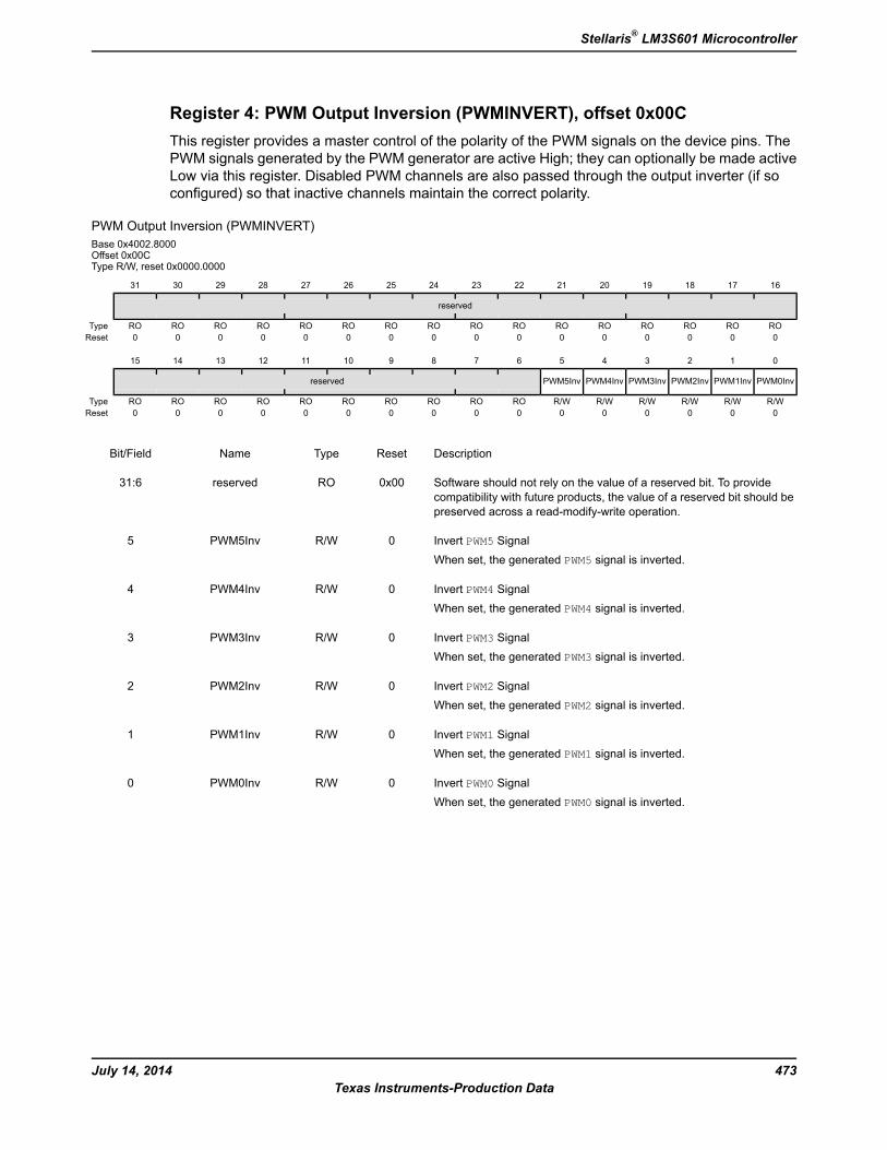
Register 4: PWM Output Inversion (PWMINVERT), offset 0x00CThis register provides a master control of the polarity of the PWM signals on the device pins. ThePWM signals generated by the PWM generator are active High; they can optionally be made activeLow via this register. Disabled PWM channels are also passed through the output inverter (if soconfigured) so that inactive channels maintain the correct polarity.
PWM Output Inversion (PWMINVERT)Base 0x4002.8000Offset 0x00CType R/W, reset 0x0000.0000
16171819202122232425262728293031
reserved
ROROROROROROROROROROROROROROROROType0000000000000000Reset
0123456789101112131415
PWM0InvPWM1InvPWM2InvPWM3InvPWM4InvPWM5Invreserved
R/WR/WR/WR/WR/WR/WROROROROROROROROROROType0000000000000000Reset
DescriptionResetTypeNameBit/Field
Software should not rely on the value of a reserved bit. To providecompatibility with future products, the value of a reserved bit should bepreserved across a read-modify-write operation.
0x00ROreserved31:6
Invert PWM5 SignalWhen set, the generated PWM5 signal is inverted.
0R/WPWM5Inv5
Invert PWM4 SignalWhen set, the generated PWM4 signal is inverted.
0R/WPWM4Inv4
Invert PWM3 SignalWhen set, the generated PWM3 signal is inverted.
0R/WPWM3Inv3
Invert PWM2 SignalWhen set, the generated PWM2 signal is inverted.
0R/WPWM2Inv2
Invert PWM1 SignalWhen set, the generated PWM1 signal is inverted.
0R/WPWM1Inv1
Invert PWM0 SignalWhen set, the generated PWM0 signal is inverted.
0R/WPWM0Inv0
473July 14, 2014Texas Instruments-Production Data
Stellaris® LM3S601 Microcontroller
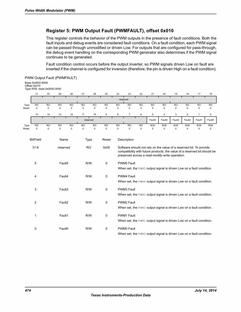
Register 5: PWM Output Fault (PWMFAULT), offset 0x010This register controls the behavior of the PWM outputs in the presence of fault conditions. Both thefault inputs and debug events are considered fault conditions. On a fault condition, each PWM signalcan be passed through unmodified or driven Low. For outputs that are configured for pass-through,the debug event handling on the corresponding PWM generator also determines if the PWM signalcontinues to be generated.
Fault condition control occurs before the output inverter, so PWM signals driven Low on fault areinverted if the channel is configured for inversion (therefore, the pin is driven High on a fault condition).
PWM Output Fault (PWMFAULT)Base 0x4002.8000Offset 0x010Type R/W, reset 0x0000.0000
16171819202122232425262728293031
reserved
ROROROROROROROROROROROROROROROROType0000000000000000Reset
0123456789101112131415
Fault0Fault1Fault2Fault3Fault4Fault5reserved
R/WR/WR/WR/WR/WR/WROROROROROROROROROROType0000000000000000Reset
DescriptionResetTypeNameBit/Field
Software should not rely on the value of a reserved bit. To providecompatibility with future products, the value of a reserved bit should bepreserved across a read-modify-write operation.
0x00ROreserved31:6
PWM5 FaultWhen set, the PWM5 output signal is driven Low on a fault condition.
0R/WFault55
PWM4 FaultWhen set, the PWM4 output signal is driven Low on a fault condition.
0R/WFault44
PWM3 FaultWhen set, the PWM3 output signal is driven Low on a fault condition.
0R/WFault33
PWM2 FaultWhen set, the PWM2 output signal is driven Low on a fault condition.
0R/WFault22
PWM1 FaultWhen set, the PWM1 output signal is driven Low on a fault condition.
0R/WFault11
PWM0 FaultWhen set, the PWM0 output signal is driven Low on a fault condition.
0R/WFault00
July 14, 2014474Texas Instruments-Production Data
Pulse Width Modulator (PWM)
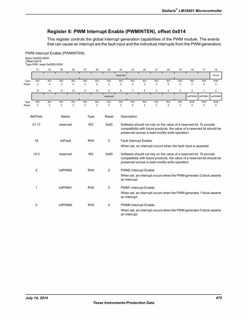
Register 6: PWM Interrupt Enable (PWMINTEN), offset 0x014This register controls the global interrupt generation capabilities of the PWM module. The eventsthat can cause an interrupt are the fault input and the individual interrupts from the PWM generators.
PWM Interrupt Enable (PWMINTEN)Base 0x4002.8000Offset 0x014Type R/W, reset 0x0000.0000
16171819202122232425262728293031
IntFaultreserved
R/WROROROROROROROROROROROROROROROType0000000000000000Reset
0123456789101112131415
IntPWM0IntPWM1IntPWM2reserved
R/WR/WR/WROROROROROROROROROROROROROType0000000000000000Reset
DescriptionResetTypeNameBit/Field
Software should not rely on the value of a reserved bit. To providecompatibility with future products, the value of a reserved bit should bepreserved across a read-modify-write operation.
0x00ROreserved31:17
Fault Interrupt EnableWhen set, an interrupt occurs when the fault input is asserted.
0R/WIntFault16
Software should not rely on the value of a reserved bit. To providecompatibility with future products, the value of a reserved bit should bepreserved across a read-modify-write operation.
0x00ROreserved15:3
PWM2 Interrupt EnableWhen set, an interrupt occurs when the PWM generator 2 block assertsan interrupt.
0R/WIntPWM22
PWM1 Interrupt EnableWhen set, an interrupt occurs when the PWM generator 1 block assertsan interrupt.
0R/WIntPWM11
PWM0 Interrupt EnableWhen set, an interrupt occurs when the PWM generator 0 block assertsan interrupt.
0R/WIntPWM00
475July 14, 2014Texas Instruments-Production Data
Stellaris® LM3S601 Microcontroller
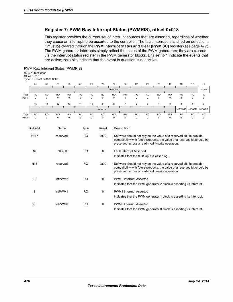
Register 7: PWM Raw Interrupt Status (PWMRIS), offset 0x018This register provides the current set of interrupt sources that are asserted, regardless of whetherthey cause an interrupt to be asserted to the controller. The fault interrupt is latched on detection;it must be cleared through the PWM Interrupt Status and Clear (PWMISC) register (see page 477).The PWM generator interrupts simply reflect the status of the PWM generators; they are clearedvia the interrupt status register in the PWM generator blocks. Bits set to 1 indicate the events thatare active; zero bits indicate that the event in question is not active.
PWM Raw Interrupt Status (PWMRIS)Base 0x4002.8000Offset 0x018Type RO, reset 0x0000.0000
16171819202122232425262728293031
IntFaultreserved
ROROROROROROROROROROROROROROROROType0000000000000000Reset
0123456789101112131415
IntPWM0IntPWM1IntPWM2reserved
ROROROROROROROROROROROROROROROROType0000000000000000Reset
DescriptionResetTypeNameBit/Field
Software should not rely on the value of a reserved bit. To providecompatibility with future products, the value of a reserved bit should bepreserved across a read-modify-write operation.
0x00ROreserved31:17
Fault Interrupt AssertedIndicates that the fault input is asserting.
0ROIntFault16
Software should not rely on the value of a reserved bit. To providecompatibility with future products, the value of a reserved bit should bepreserved across a read-modify-write operation.
0x00ROreserved15:3
PWM2 Interrupt AssertedIndicates that the PWM generator 2 block is asserting its interrupt.
0ROIntPWM22
PWM1 Interrupt AssertedIndicates that the PWM generator 1 block is asserting its interrupt.
0ROIntPWM11
PWM0 Interrupt AssertedIndicates that the PWM generator 0 block is asserting its interrupt.
0ROIntPWM00
July 14, 2014476Texas Instruments-Production Data
Pulse Width Modulator (PWM)
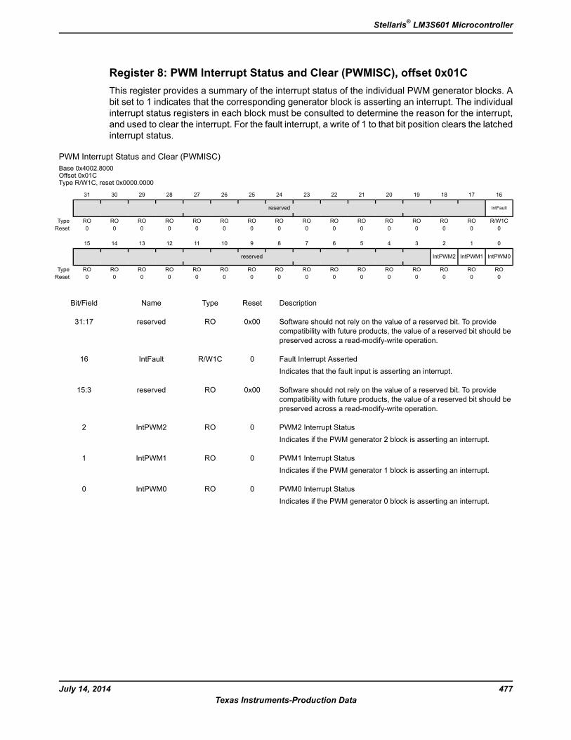
Register 8: PWM Interrupt Status and Clear (PWMISC), offset 0x01CThis register provides a summary of the interrupt status of the individual PWM generator blocks. Abit set to 1 indicates that the corresponding generator block is asserting an interrupt. The individualinterrupt status registers in each block must be consulted to determine the reason for the interrupt,and used to clear the interrupt. For the fault interrupt, a write of 1 to that bit position clears the latchedinterrupt status.
PWM Interrupt Status and Clear (PWMISC)Base 0x4002.8000Offset 0x01CType R/W1C, reset 0x0000.0000
16171819202122232425262728293031
IntFaultreserved
R/W1CROROROROROROROROROROROROROROROType0000000000000000Reset
0123456789101112131415
IntPWM0IntPWM1IntPWM2reserved
ROROROROROROROROROROROROROROROROType0000000000000000Reset
DescriptionResetTypeNameBit/Field
Software should not rely on the value of a reserved bit. To providecompatibility with future products, the value of a reserved bit should bepreserved across a read-modify-write operation.
0x00ROreserved31:17
Fault Interrupt AssertedIndicates that the fault input is asserting an interrupt.
0R/W1CIntFault16
Software should not rely on the value of a reserved bit. To providecompatibility with future products, the value of a reserved bit should bepreserved across a read-modify-write operation.
0x00ROreserved15:3
PWM2 Interrupt StatusIndicates if the PWM generator 2 block is asserting an interrupt.
0ROIntPWM22
PWM1 Interrupt StatusIndicates if the PWM generator 1 block is asserting an interrupt.
0ROIntPWM11
PWM0 Interrupt StatusIndicates if the PWM generator 0 block is asserting an interrupt.
0ROIntPWM00
477July 14, 2014Texas Instruments-Production Data
Stellaris® LM3S601 Microcontroller
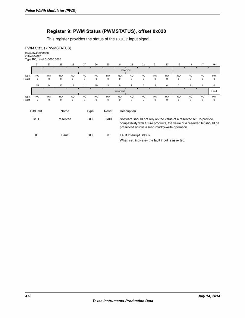
Register 9: PWM Status (PWMSTATUS), offset 0x020This register provides the status of the FAULT input signal.
PWM Status (PWMSTATUS)Base 0x4002.8000Offset 0x020Type RO, reset 0x0000.0000
16171819202122232425262728293031
reserved
ROROROROROROROROROROROROROROROROType0000000000000000Reset
0123456789101112131415
Faultreserved
ROROROROROROROROROROROROROROROROType0000000000000000Reset
DescriptionResetTypeNameBit/Field
Software should not rely on the value of a reserved bit. To providecompatibility with future products, the value of a reserved bit should bepreserved across a read-modify-write operation.
0x00ROreserved31:1
Fault Interrupt StatusWhen set, indicates the fault input is asserted.
0ROFault0
July 14, 2014478Texas Instruments-Production Data
Pulse Width Modulator (PWM)
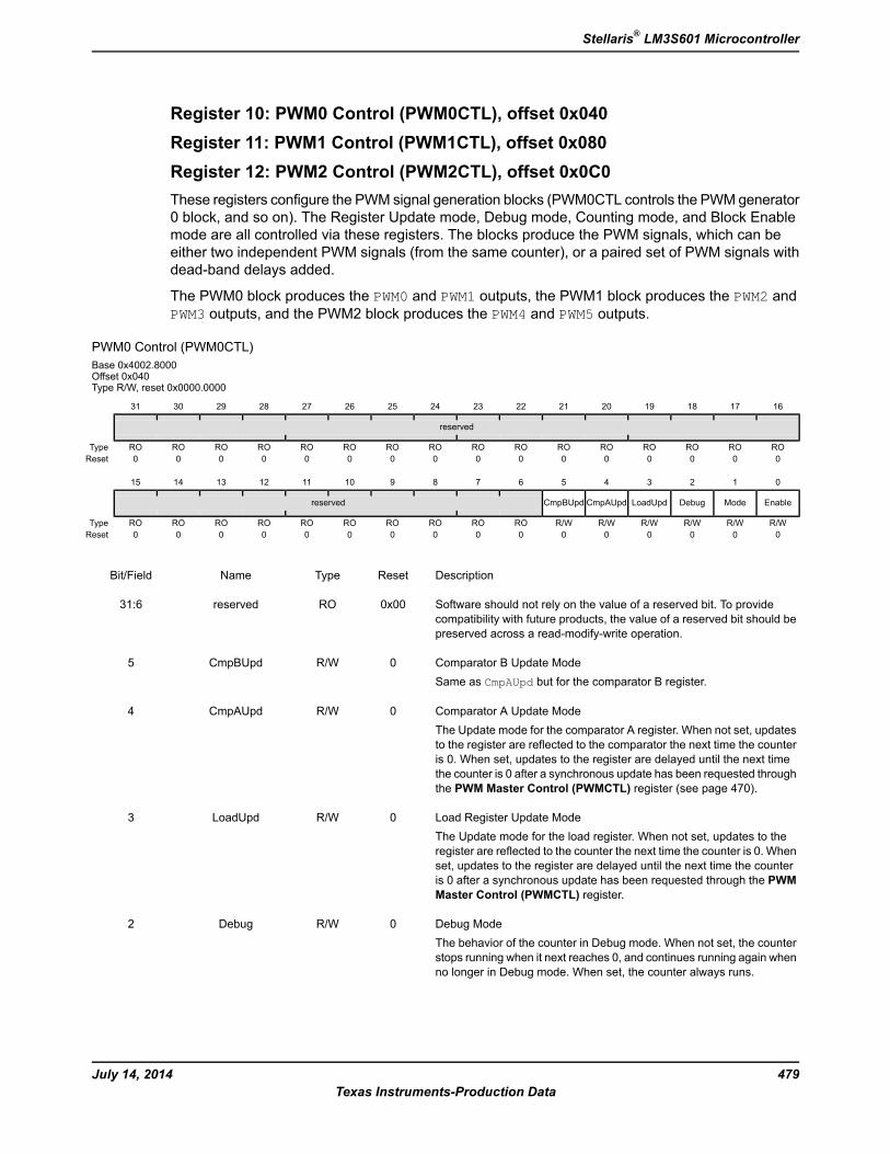
Register 10: PWM0 Control (PWM0CTL), offset 0x040Register 11: PWM1 Control (PWM1CTL), offset 0x080Register 12: PWM2 Control (PWM2CTL), offset 0x0C0These registers configure the PWM signal generation blocks (PWM0CTL controls the PWMgenerator0 block, and so on). The Register Update mode, Debug mode, Counting mode, and Block Enablemode are all controlled via these registers. The blocks produce the PWM signals, which can beeither two independent PWM signals (from the same counter), or a paired set of PWM signals withdead-band delays added.
The PWM0 block produces the PWM0 and PWM1 outputs, the PWM1 block produces the PWM2 andPWM3 outputs, and the PWM2 block produces the PWM4 and PWM5 outputs.
PWM0 Control (PWM0CTL)Base 0x4002.8000Offset 0x040Type R/W, reset 0x0000.0000
16171819202122232425262728293031
reserved
ROROROROROROROROROROROROROROROROType0000000000000000Reset
0123456789101112131415
EnableModeDebugLoadUpdCmpAUpdCmpBUpdreserved
R/WR/WR/WR/WR/WR/WROROROROROROROROROROType0000000000000000Reset
DescriptionResetTypeNameBit/Field
Software should not rely on the value of a reserved bit. To providecompatibility with future products, the value of a reserved bit should bepreserved across a read-modify-write operation.
0x00ROreserved31:6
Comparator B Update ModeSame as CmpAUpd but for the comparator B register.
0R/WCmpBUpd5
Comparator A Update ModeThe Update mode for the comparator A register. When not set, updatesto the register are reflected to the comparator the next time the counteris 0. When set, updates to the register are delayed until the next timethe counter is 0 after a synchronous update has been requested throughthe PWM Master Control (PWMCTL) register (see page 470).
0R/WCmpAUpd4
Load Register Update ModeThe Update mode for the load register. When not set, updates to theregister are reflected to the counter the next time the counter is 0. Whenset, updates to the register are delayed until the next time the counteris 0 after a synchronous update has been requested through the PWMMaster Control (PWMCTL) register.
0R/WLoadUpd3
Debug ModeThe behavior of the counter in Debug mode. When not set, the counterstops running when it next reaches 0, and continues running again whenno longer in Debug mode. When set, the counter always runs.
0R/WDebug2
479July 14, 2014Texas Instruments-Production Data
Stellaris® LM3S601 Microcontroller
DescriptionResetTypeNameBit/Field
Counter ModeThe mode for the counter. When not set, the counter counts down fromthe load value to 0 and then wraps back to the load value (Count-Downmode). When set, the counter counts up from 0 to the load value, backdown to 0, and then repeats (Count-Up/Down mode).
0R/WMode1
PWM Block EnableMaster enable for the PWM generation block. When not set, the entireblock is disabled and not clocked. When set, the block is enabled andproduces PWM signals.
0R/WEnable0
July 14, 2014480Texas Instruments-Production Data
Pulse Width Modulator (PWM)
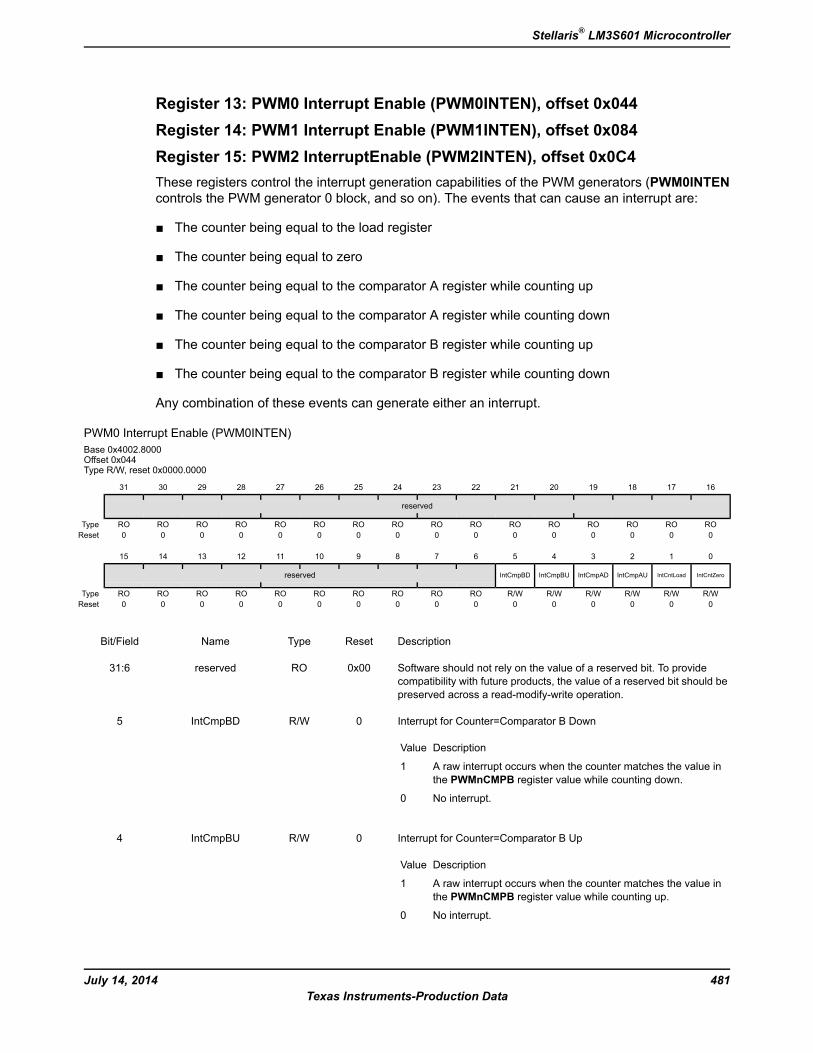
Register 13: PWM0 Interrupt Enable (PWM0INTEN), offset 0x044Register 14: PWM1 Interrupt Enable (PWM1INTEN), offset 0x084Register 15: PWM2 InterruptEnable (PWM2INTEN), offset 0x0C4These registers control the interrupt generation capabilities of the PWM generators (PWM0INTENcontrols the PWM generator 0 block, and so on). The events that can cause an interrupt are:
The counter being equal to the load register
The counter being equal to zero
The counter being equal to the comparator A register while counting up
The counter being equal to the comparator A register while counting down
The counter being equal to the comparator B register while counting up
The counter being equal to the comparator B register while counting down
Any combination of these events can generate either an interrupt.
PWM0 Interrupt Enable (PWM0INTEN)Base 0x4002.8000Offset 0x044Type R/W, reset 0x0000.0000
16171819202122232425262728293031
reserved
ROROROROROROROROROROROROROROROROType0000000000000000Reset
0123456789101112131415
IntCntZeroIntCntLoadIntCmpAUIntCmpADIntCmpBUIntCmpBDreserved
R/WR/WR/WR/WR/WR/WROROROROROROROROROROType0000000000000000Reset
DescriptionResetTypeNameBit/Field
Software should not rely on the value of a reserved bit. To providecompatibility with future products, the value of a reserved bit should bepreserved across a read-modify-write operation.
0x00ROreserved31:6
Interrupt for Counter=Comparator B Down
DescriptionValue
A raw interrupt occurs when the counter matches the value inthe PWMnCMPB register value while counting down.
1
No interrupt.0
0R/WIntCmpBD5
Interrupt for Counter=Comparator B Up
DescriptionValue
A raw interrupt occurs when the counter matches the value inthe PWMnCMPB register value while counting up.
1
No interrupt.0
0R/WIntCmpBU4
481July 14, 2014Texas Instruments-Production Data
Stellaris® LM3S601 Microcontroller
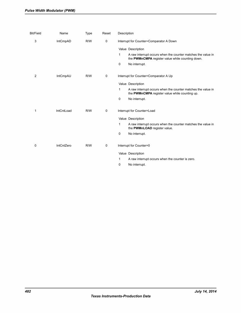
DescriptionResetTypeNameBit/Field
Interrupt for Counter=Comparator A Down
DescriptionValue
A raw interrupt occurs when the counter matches the value inthe PWMnCMPA register value while counting down.
1
No interrupt.0
0R/WIntCmpAD3
Interrupt for Counter=Comparator A Up
DescriptionValue
A raw interrupt occurs when the counter matches the value inthe PWMnCMPA register value while counting up.
1
No interrupt.0
0R/WIntCmpAU2
Interrupt for Counter=Load
DescriptionValue
A raw interrupt occurs when the counter matches the value inthe PWMnLOAD register value.
1
No interrupt.0
0R/WIntCntLoad1
Interrupt for Counter=0
DescriptionValue
A raw interrupt occurs when the counter is zero.1
No interrupt.0
0R/WIntCntZero0
July 14, 2014482Texas Instruments-Production Data
Pulse Width Modulator (PWM)
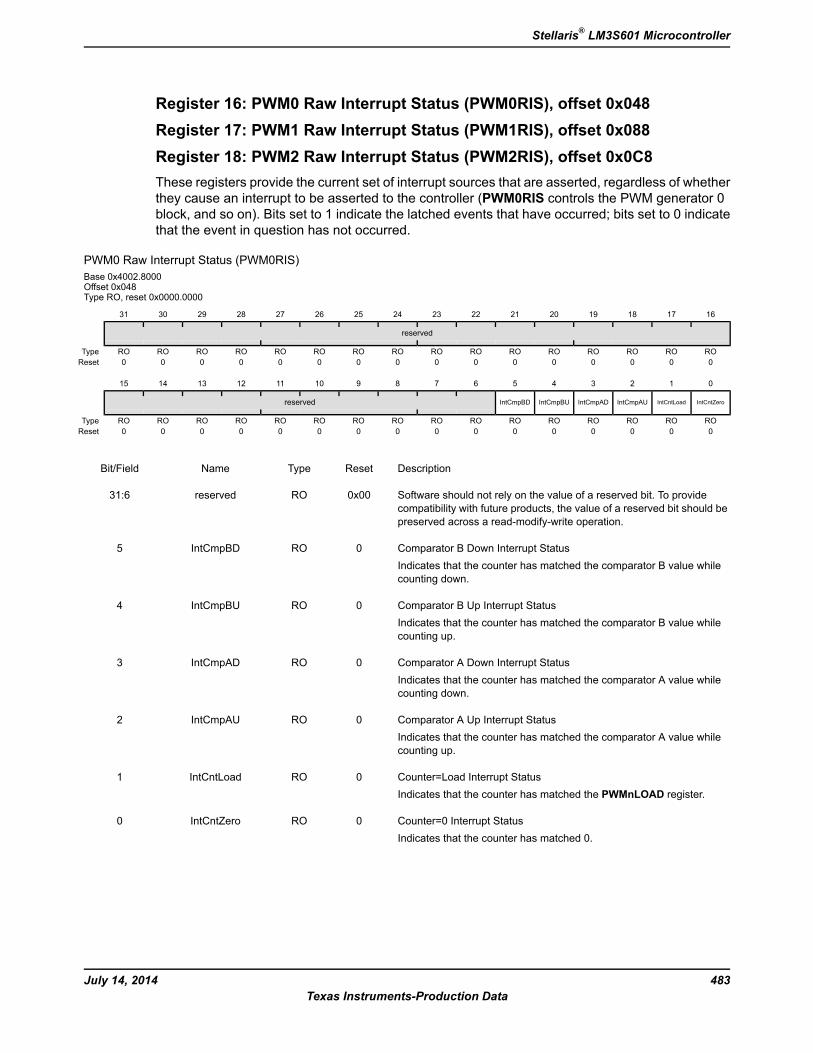
Register 16: PWM0 Raw Interrupt Status (PWM0RIS), offset 0x048Register 17: PWM1 Raw Interrupt Status (PWM1RIS), offset 0x088Register 18: PWM2 Raw Interrupt Status (PWM2RIS), offset 0x0C8These registers provide the current set of interrupt sources that are asserted, regardless of whetherthey cause an interrupt to be asserted to the controller (PWM0RIS controls the PWM generator 0block, and so on). Bits set to 1 indicate the latched events that have occurred; bits set to 0 indicatethat the event in question has not occurred.
PWM0 Raw Interrupt Status (PWM0RIS)Base 0x4002.8000Offset 0x048Type RO, reset 0x0000.0000
16171819202122232425262728293031
reserved
ROROROROROROROROROROROROROROROROType0000000000000000Reset
0123456789101112131415
IntCntZeroIntCntLoadIntCmpAUIntCmpADIntCmpBUIntCmpBDreserved
ROROROROROROROROROROROROROROROROType0000000000000000Reset
DescriptionResetTypeNameBit/Field
Software should not rely on the value of a reserved bit. To providecompatibility with future products, the value of a reserved bit should bepreserved across a read-modify-write operation.
0x00ROreserved31:6
Comparator B Down Interrupt StatusIndicates that the counter has matched the comparator B value whilecounting down.
0ROIntCmpBD5
Comparator B Up Interrupt StatusIndicates that the counter has matched the comparator B value whilecounting up.
0ROIntCmpBU4
Comparator A Down Interrupt StatusIndicates that the counter has matched the comparator A value whilecounting down.
0ROIntCmpAD3
Comparator A Up Interrupt StatusIndicates that the counter has matched the comparator A value whilecounting up.
0ROIntCmpAU2
Counter=Load Interrupt StatusIndicates that the counter has matched the PWMnLOAD register.
0ROIntCntLoad1
Counter=0 Interrupt StatusIndicates that the counter has matched 0.
0ROIntCntZero0
483July 14, 2014Texas Instruments-Production Data
Stellaris® LM3S601 Microcontroller
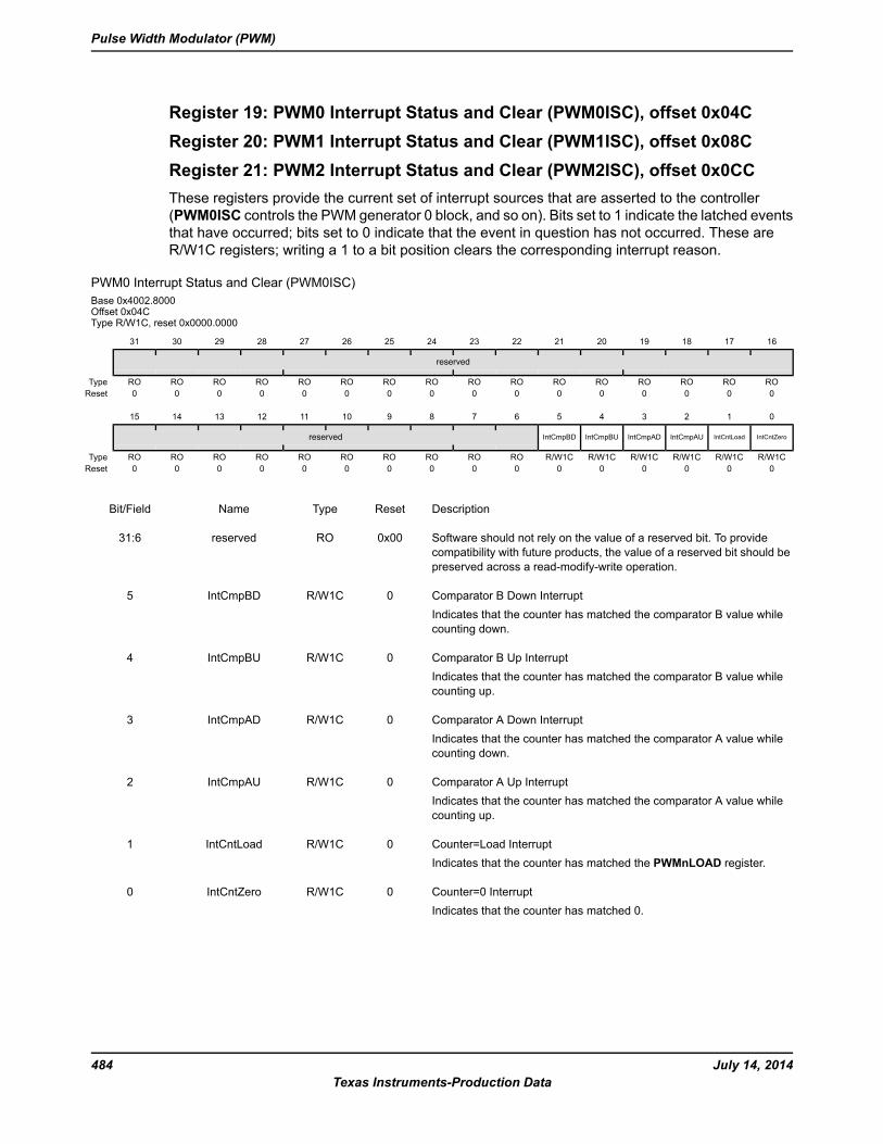
Register 19: PWM0 Interrupt Status and Clear (PWM0ISC), offset 0x04CRegister 20: PWM1 Interrupt Status and Clear (PWM1ISC), offset 0x08CRegister 21: PWM2 Interrupt Status and Clear (PWM2ISC), offset 0x0CCThese registers provide the current set of interrupt sources that are asserted to the controller(PWM0ISC controls the PWM generator 0 block, and so on). Bits set to 1 indicate the latched eventsthat have occurred; bits set to 0 indicate that the event in question has not occurred. These areR/W1C registers; writing a 1 to a bit position clears the corresponding interrupt reason.
PWM0 Interrupt Status and Clear (PWM0ISC)Base 0x4002.8000Offset 0x04CType R/W1C, reset 0x0000.0000
16171819202122232425262728293031
reserved
ROROROROROROROROROROROROROROROROType0000000000000000Reset
0123456789101112131415
IntCntZeroIntCntLoadIntCmpAUIntCmpADIntCmpBUIntCmpBDreserved
R/W1CR/W1CR/W1CR/W1CR/W1CR/W1CROROROROROROROROROROType0000000000000000Reset
DescriptionResetTypeNameBit/Field
Software should not rely on the value of a reserved bit. To providecompatibility with future products, the value of a reserved bit should bepreserved across a read-modify-write operation.
0x00ROreserved31:6
Comparator B Down InterruptIndicates that the counter has matched the comparator B value whilecounting down.
0R/W1CIntCmpBD5
Comparator B Up InterruptIndicates that the counter has matched the comparator B value whilecounting up.
0R/W1CIntCmpBU4
Comparator A Down InterruptIndicates that the counter has matched the comparator A value whilecounting down.
0R/W1CIntCmpAD3
Comparator A Up InterruptIndicates that the counter has matched the comparator A value whilecounting up.
0R/W1CIntCmpAU2
Counter=Load InterruptIndicates that the counter has matched the PWMnLOAD register.
0R/W1CIntCntLoad1
Counter=0 InterruptIndicates that the counter has matched 0.
0R/W1CIntCntZero0
July 14, 2014484Texas Instruments-Production Data
Pulse Width Modulator (PWM)
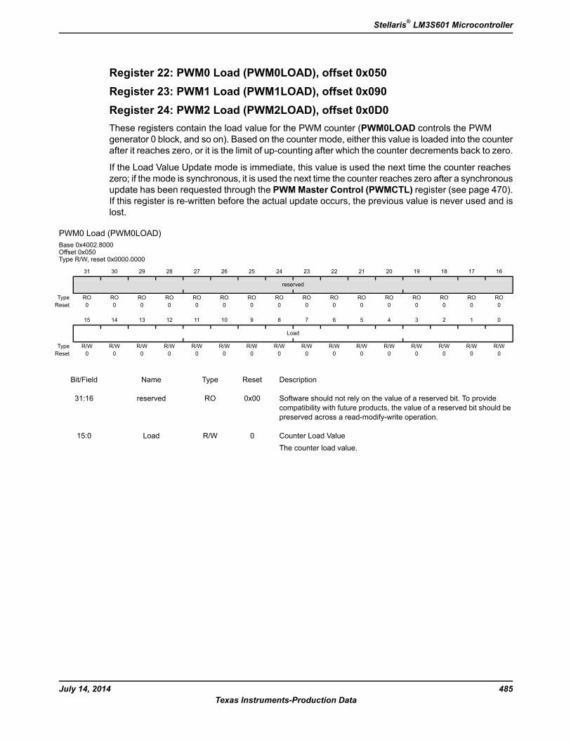
Register 22: PWM0 Load (PWM0LOAD), offset 0x050Register 23: PWM1 Load (PWM1LOAD), offset 0x090Register 24: PWM2 Load (PWM2LOAD), offset 0x0D0These registers contain the load value for the PWM counter (PWM0LOAD controls the PWMgenerator 0 block, and so on). Based on the counter mode, either this value is loaded into the counterafter it reaches zero, or it is the limit of up-counting after which the counter decrements back to zero.
If the Load Value Update mode is immediate, this value is used the next time the counter reacheszero; if the mode is synchronous, it is used the next time the counter reaches zero after a synchronousupdate has been requested through the PWMMaster Control (PWMCTL) register (see page 470).If this register is re-written before the actual update occurs, the previous value is never used and islost.
PWM0 Load (PWM0LOAD)Base 0x4002.8000Offset 0x050Type R/W, reset 0x0000.0000
16171819202122232425262728293031
reserved
ROROROROROROROROROROROROROROROROType0000000000000000Reset
0123456789101112131415
Load
R/WR/WR/WR/WR/WR/WR/WR/WR/WR/WR/WR/WR/WR/WR/WR/WType0000000000000000Reset
DescriptionResetTypeNameBit/Field
Software should not rely on the value of a reserved bit. To providecompatibility with future products, the value of a reserved bit should bepreserved across a read-modify-write operation.
0x00ROreserved31:16
Counter Load ValueThe counter load value.
0R/WLoad15:0
485July 14, 2014Texas Instruments-Production Data
Stellaris® LM3S601 Microcontroller
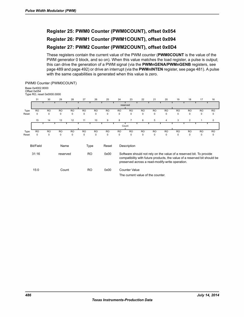
Register 25: PWM0 Counter (PWM0COUNT), offset 0x054Register 26: PWM1 Counter (PWM1COUNT), offset 0x094Register 27: PWM2 Counter (PWM2COUNT), offset 0x0D4These registers contain the current value of the PWM counter (PWM0COUNT is the value of thePWM generator 0 block, and so on). When this value matches the load register, a pulse is output;this can drive the generation of a PWM signal (via the PWMnGENA/PWMnGENB registers, seepage 489 and page 492) or drive an interrupt (via the PWMnINTEN register, see page 481). A pulsewith the same capabilities is generated when this value is zero.
PWM0 Counter (PWM0COUNT)Base 0x4002.8000Offset 0x054Type RO, reset 0x0000.0000
16171819202122232425262728293031
reserved
ROROROROROROROROROROROROROROROROType0000000000000000Reset
0123456789101112131415
Count
ROROROROROROROROROROROROROROROROType0000000000000000Reset
DescriptionResetTypeNameBit/Field
Software should not rely on the value of a reserved bit. To providecompatibility with future products, the value of a reserved bit should bepreserved across a read-modify-write operation.
0x00ROreserved31:16
Counter ValueThe current value of the counter.
0x00ROCount15:0
July 14, 2014486Texas Instruments-Production Data
Pulse Width Modulator (PWM)
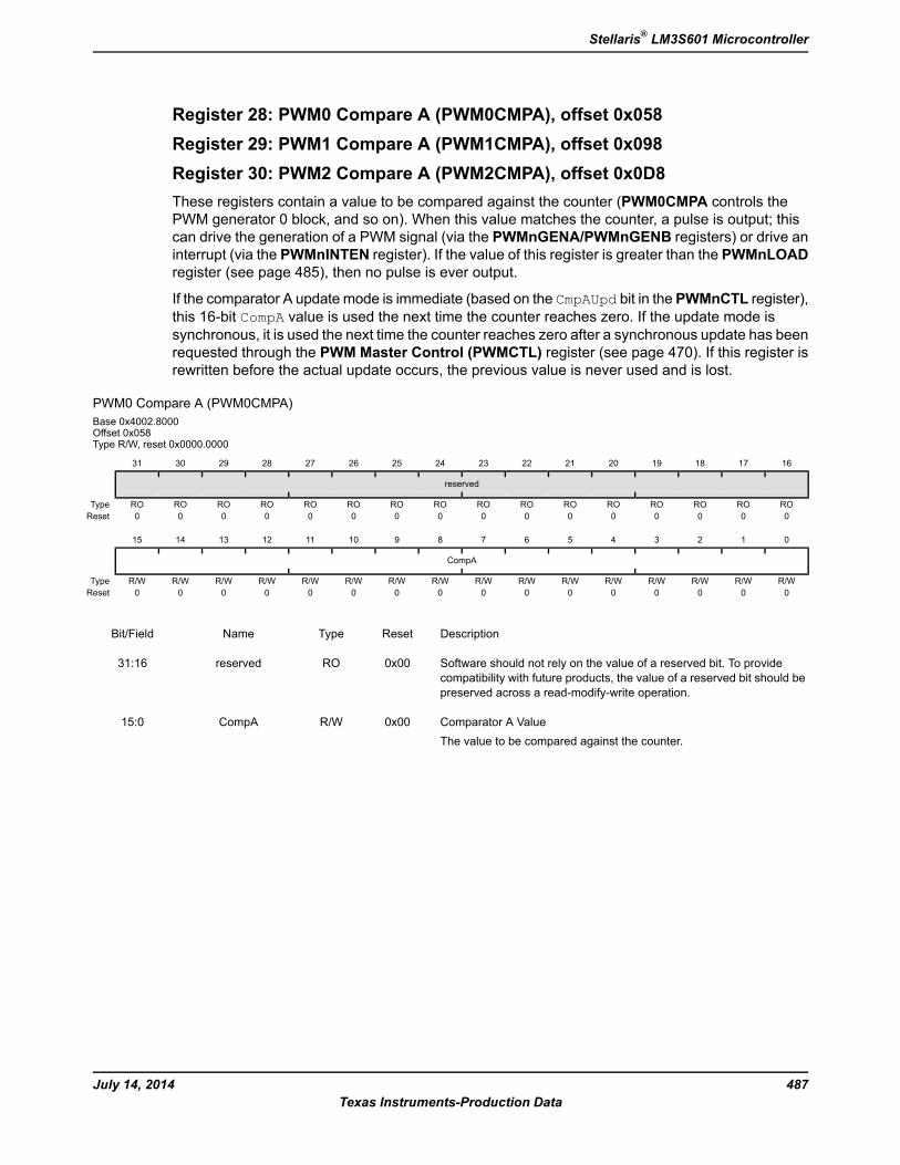
Register 28: PWM0 Compare A (PWM0CMPA), offset 0x058Register 29: PWM1 Compare A (PWM1CMPA), offset 0x098Register 30: PWM2 Compare A (PWM2CMPA), offset 0x0D8These registers contain a value to be compared against the counter (PWM0CMPA controls thePWM generator 0 block, and so on). When this value matches the counter, a pulse is output; thiscan drive the generation of a PWM signal (via the PWMnGENA/PWMnGENB registers) or drive aninterrupt (via the PWMnINTEN register). If the value of this register is greater than the PWMnLOADregister (see page 485), then no pulse is ever output.
If the comparator A update mode is immediate (based on the CmpAUpd bit in the PWMnCTL register),this 16-bit CompA value is used the next time the counter reaches zero. If the update mode issynchronous, it is used the next time the counter reaches zero after a synchronous update has beenrequested through the PWM Master Control (PWMCTL) register (see page 470). If this register isrewritten before the actual update occurs, the previous value is never used and is lost.
PWM0 Compare A (PWM0CMPA)Base 0x4002.8000Offset 0x058Type R/W, reset 0x0000.0000
16171819202122232425262728293031
reserved
ROROROROROROROROROROROROROROROROType0000000000000000Reset
0123456789101112131415
CompA
R/WR/WR/WR/WR/WR/WR/WR/WR/WR/WR/WR/WR/WR/WR/WR/WType0000000000000000Reset
DescriptionResetTypeNameBit/Field
Software should not rely on the value of a reserved bit. To providecompatibility with future products, the value of a reserved bit should bepreserved across a read-modify-write operation.
0x00ROreserved31:16
Comparator A ValueThe value to be compared against the counter.
0x00R/WCompA15:0
487July 14, 2014Texas Instruments-Production Data
Stellaris® LM3S601 Microcontroller
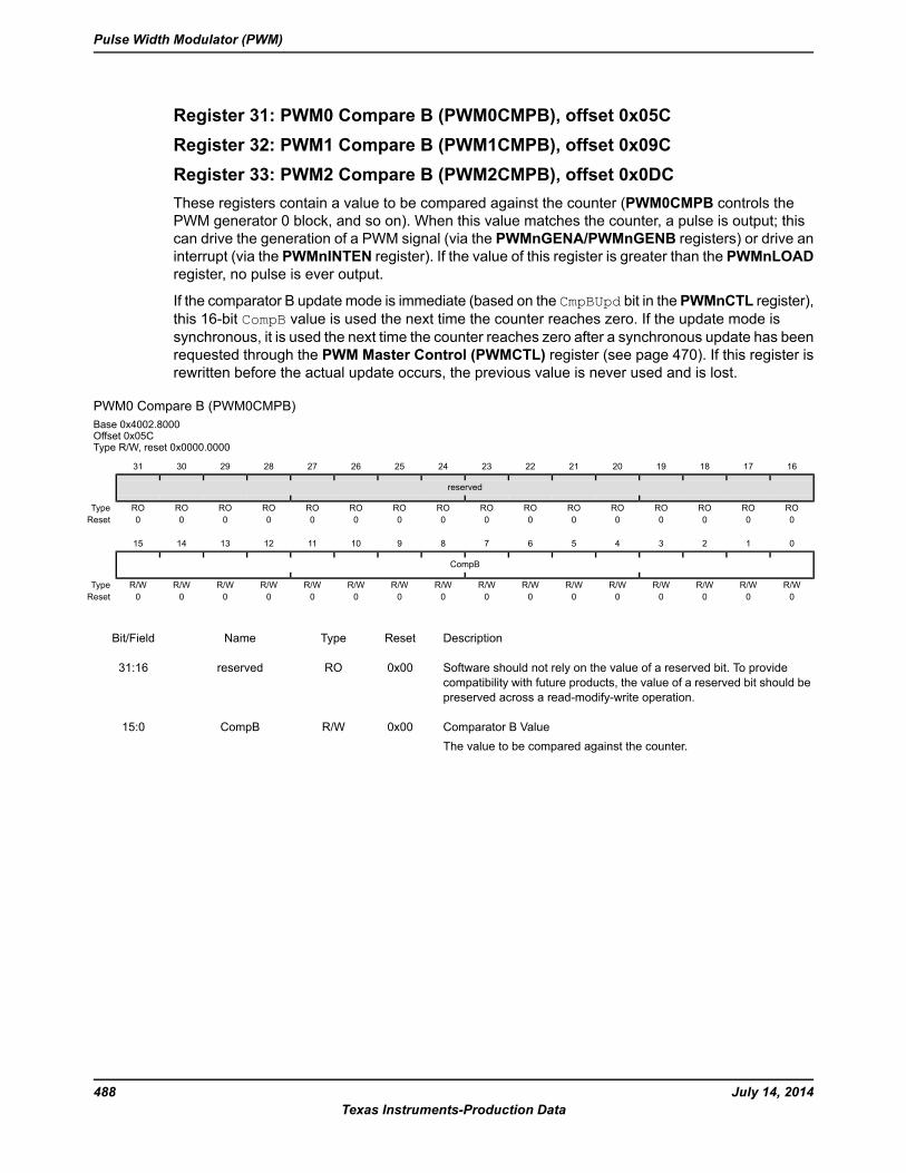
Register 31: PWM0 Compare B (PWM0CMPB), offset 0x05CRegister 32: PWM1 Compare B (PWM1CMPB), offset 0x09CRegister 33: PWM2 Compare B (PWM2CMPB), offset 0x0DCThese registers contain a value to be compared against the counter (PWM0CMPB controls thePWM generator 0 block, and so on). When this value matches the counter, a pulse is output; thiscan drive the generation of a PWM signal (via the PWMnGENA/PWMnGENB registers) or drive aninterrupt (via the PWMnINTEN register). If the value of this register is greater than the PWMnLOADregister, no pulse is ever output.
If the comparator B update mode is immediate (based on the CmpBUpd bit in the PWMnCTL register),this 16-bit CompB value is used the next time the counter reaches zero. If the update mode issynchronous, it is used the next time the counter reaches zero after a synchronous update has beenrequested through the PWM Master Control (PWMCTL) register (see page 470). If this register isrewritten before the actual update occurs, the previous value is never used and is lost.
PWM0 Compare B (PWM0CMPB)Base 0x4002.8000Offset 0x05CType R/W, reset 0x0000.0000
16171819202122232425262728293031
reserved
ROROROROROROROROROROROROROROROROType0000000000000000Reset
0123456789101112131415
CompB
R/WR/WR/WR/WR/WR/WR/WR/WR/WR/WR/WR/WR/WR/WR/WR/WType0000000000000000Reset
DescriptionResetTypeNameBit/Field
Software should not rely on the value of a reserved bit. To providecompatibility with future products, the value of a reserved bit should bepreserved across a read-modify-write operation.
0x00ROreserved31:16
Comparator B ValueThe value to be compared against the counter.
0x00R/WCompB15:0
July 14, 2014488Texas Instruments-Production Data
Pulse Width Modulator (PWM)
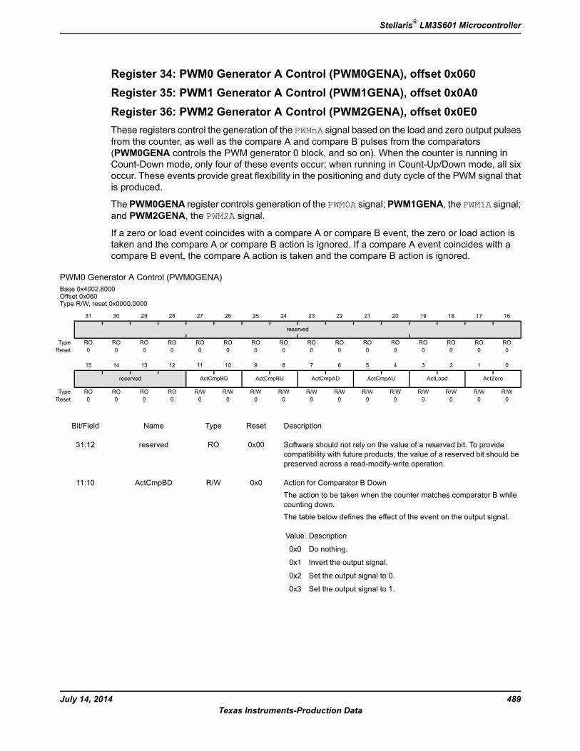
Register 34: PWM0 Generator A Control (PWM0GENA), offset 0x060Register 35: PWM1 Generator A Control (PWM1GENA), offset 0x0A0Register 36: PWM2 Generator A Control (PWM2GENA), offset 0x0E0These registers control the generation of the PWMnA signal based on the load and zero output pulsesfrom the counter, as well as the compare A and compare B pulses from the comparators(PWM0GENA controls the PWM generator 0 block, and so on). When the counter is running inCount-Down mode, only four of these events occur; when running in Count-Up/Down mode, all sixoccur. These events provide great flexibility in the positioning and duty cycle of the PWM signal thatis produced.
The PWM0GENA register controls generation of the PWM0A signal; PWM1GENA, the PWM1A signal;and PWM2GENA, the PWM2A signal.
If a zero or load event coincides with a compare A or compare B event, the zero or load action istaken and the compare A or compare B action is ignored. If a compare A event coincides with acompare B event, the compare A action is taken and the compare B action is ignored.
PWM0 Generator A Control (PWM0GENA)Base 0x4002.8000Offset 0x060Type R/W, reset 0x0000.0000
16171819202122232425262728293031
reserved
ROROROROROROROROROROROROROROROROType0000000000000000Reset
0123456789101112131415
ActZeroActLoadActCmpAUActCmpADActCmpBUActCmpBDreserved
R/WR/WR/WR/WR/WR/WR/WR/WR/WR/WR/WR/WROROROROType0000000000000000Reset
DescriptionResetTypeNameBit/Field
Software should not rely on the value of a reserved bit. To providecompatibility with future products, the value of a reserved bit should bepreserved across a read-modify-write operation.
0x00ROreserved31:12
Action for Comparator B DownThe action to be taken when the counter matches comparator B whilecounting down.The table below defines the effect of the event on the output signal.
DescriptionValue
Do nothing.0x0
Invert the output signal.0x1
Set the output signal to 0.0x2
Set the output signal to 1.0x3
0x0R/WActCmpBD11:10
489July 14, 2014Texas Instruments-Production Data
Stellaris® LM3S601 Microcontroller
DescriptionResetTypeNameBit/Field
Action for Comparator B UpThe action to be taken when the counter matches comparator B whilecounting up. Occurs only when the Mode bit in the PWMnCTL register(see page 479) is set to 1.The table below defines the effect of the event on the output signal.
DescriptionValue
Do nothing.0x0
Invert the output signal.0x1
Set the output signal to 0.0x2
Set the output signal to 1.0x3
0x0R/WActCmpBU9:8
Action for Comparator A DownThe action to be taken when the counter matches comparator A whilecounting down.The table below defines the effect of the event on the output signal.
DescriptionValue
Do nothing.0x0
Invert the output signal.0x1
Set the output signal to 0.0x2
Set the output signal to 1.0x3
0x0R/WActCmpAD7:6
Action for Comparator A UpThe action to be taken when the counter matches comparator A whilecounting up. Occurs only when the Mode bit in the PWMnCTL registeris set to 1.The table below defines the effect of the event on the output signal.
DescriptionValue
Do nothing.0x0
Invert the output signal.0x1
Set the output signal to 0.0x2
Set the output signal to 1.0x3
0x0R/WActCmpAU5:4
Action for Counter=LoadThe action to be taken when the counter matches the load value.The table below defines the effect of the event on the output signal.
DescriptionValue
Do nothing.0x0
Invert the output signal.0x1
Set the output signal to 0.0x2
Set the output signal to 1.0x3
0x0R/WActLoad3:2
July 14, 2014490Texas Instruments-Production Data
Pulse Width Modulator (PWM)
DescriptionResetTypeNameBit/Field
Action for Counter=0The action to be taken when the counter is zero.The table below defines the effect of the event on the output signal.
DescriptionValue
Do nothing.0x0
Invert the output signal.0x1
Set the output signal to 0.0x2
Set the output signal to 1.0x3
0x0R/WActZero1:0
491July 14, 2014Texas Instruments-Production Data
Stellaris® LM3S601 Microcontroller
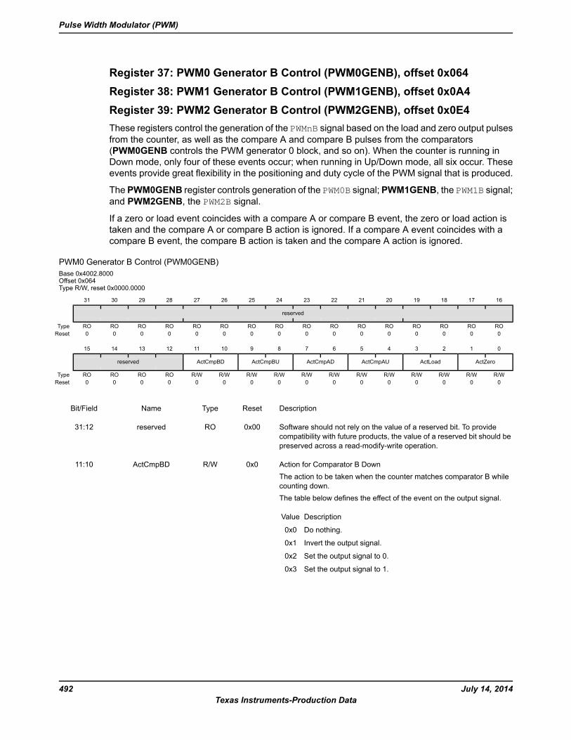
Register 37: PWM0 Generator B Control (PWM0GENB), offset 0x064Register 38: PWM1 Generator B Control (PWM1GENB), offset 0x0A4Register 39: PWM2 Generator B Control (PWM2GENB), offset 0x0E4These registers control the generation of the PWMnB signal based on the load and zero output pulsesfrom the counter, as well as the compare A and compare B pulses from the comparators(PWM0GENB controls the PWM generator 0 block, and so on). When the counter is running inDown mode, only four of these events occur; when running in Up/Down mode, all six occur. Theseevents provide great flexibility in the positioning and duty cycle of the PWM signal that is produced.
The PWM0GENB register controls generation of the PWM0B signal; PWM1GENB, the PWM1B signal;and PWM2GENB, the PWM2B signal.
If a zero or load event coincides with a compare A or compare B event, the zero or load action istaken and the compare A or compare B action is ignored. If a compare A event coincides with acompare B event, the compare B action is taken and the compare A action is ignored.
PWM0 Generator B Control (PWM0GENB)Base 0x4002.8000Offset 0x064Type R/W, reset 0x0000.0000
16171819202122232425262728293031
reserved
ROROROROROROROROROROROROROROROROType0000000000000000Reset
0123456789101112131415
ActZeroActLoadActCmpAUActCmpADActCmpBUActCmpBDreserved
R/WR/WR/WR/WR/WR/WR/WR/WR/WR/WR/WR/WROROROROType0000000000000000Reset
DescriptionResetTypeNameBit/Field
Software should not rely on the value of a reserved bit. To providecompatibility with future products, the value of a reserved bit should bepreserved across a read-modify-write operation.
0x00ROreserved31:12
Action for Comparator B DownThe action to be taken when the counter matches comparator B whilecounting down.The table below defines the effect of the event on the output signal.
DescriptionValue
Do nothing.0x0
Invert the output signal.0x1
Set the output signal to 0.0x2
Set the output signal to 1.0x3
0x0R/WActCmpBD11:10
July 14, 2014492Texas Instruments-Production Data
Pulse Width Modulator (PWM)
DescriptionResetTypeNameBit/Field
Action for Comparator B UpThe action to be taken when the counter matches comparator B whilecounting up. Occurs only when the Mode bit in the PWMnCTL registeris set to 1.The table below defines the effect of the event on the output signal.
DescriptionValue
Do nothing.0x0
Invert the output signal.0x1
Set the output signal to 0.0x2
Set the output signal to 1.0x3
0x0R/WActCmpBU9:8
Action for Comparator A DownThe action to be taken when the counter matches comparator A whilecounting down.The table below defines the effect of the event on the output signal.
DescriptionValue
Do nothing.0x0
Invert the output signal.0x1
Set the output signal to 0.0x2
Set the output signal to 1.0x3
0x0R/WActCmpAD7:6
Action for Comparator A UpThe action to be taken when the counter matches comparator A whilecounting up. Occurs only when the Mode bit in the PWMnCTL registeris set to 1.The table below defines the effect of the event on the output signal.
DescriptionValue
Do nothing.0x0
Invert the output signal.0x1
Set the output signal to 0.0x2
Set the output signal to 1.0x3
0x0R/WActCmpAU5:4
Action for Counter=LoadThe action to be taken when the counter matches the load value.The table below defines the effect of the event on the output signal.
DescriptionValue
Do nothing.0x0
Invert the output signal.0x1
Set the output signal to 0.0x2
Set the output signal to 1.0x3
0x0R/WActLoad3:2
493July 14, 2014Texas Instruments-Production Data
Stellaris® LM3S601 Microcontroller
DescriptionResetTypeNameBit/Field
Action for Counter=0The action to be taken when the counter is 0.The table below defines the effect of the event on the output signal.
DescriptionValue
Do nothing.0x0
Invert the output signal.0x1
Set the output signal to 0.0x2
Set the output signal to 1.0x3
0x0R/WActZero1:0
July 14, 2014494Texas Instruments-Production Data
Pulse Width Modulator (PWM)
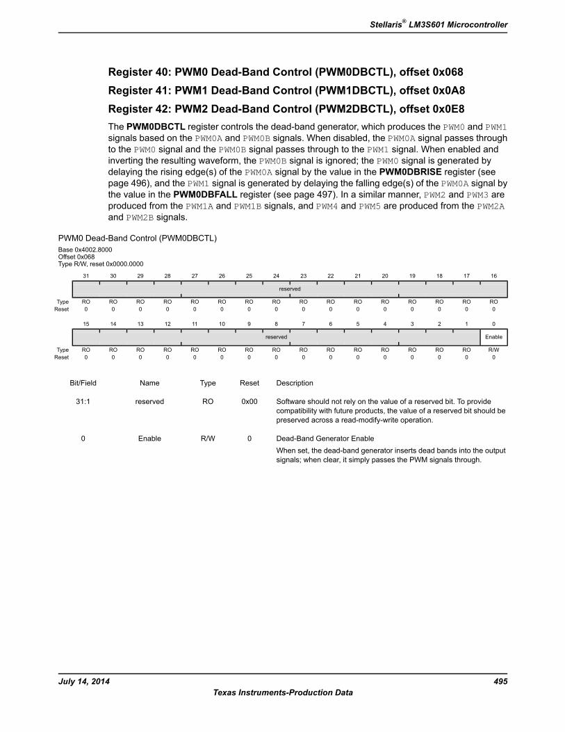
Register 40: PWM0 Dead-Band Control (PWM0DBCTL), offset 0x068Register 41: PWM1 Dead-Band Control (PWM1DBCTL), offset 0x0A8Register 42: PWM2 Dead-Band Control (PWM2DBCTL), offset 0x0E8The PWM0DBCTL register controls the dead-band generator, which produces the PWM0 and PWM1signals based on the PWM0A and PWM0B signals. When disabled, the PWM0A signal passes throughto the PWM0 signal and the PWM0B signal passes through to the PWM1 signal. When enabled andinverting the resulting waveform, the PWM0B signal is ignored; the PWM0 signal is generated bydelaying the rising edge(s) of the PWM0A signal by the value in the PWM0DBRISE register (seepage 496), and the PWM1 signal is generated by delaying the falling edge(s) of the PWM0A signal bythe value in the PWM0DBFALL register (see page 497). In a similar manner, PWM2 and PWM3 areproduced from the PWM1A and PWM1B signals, and PWM4 and PWM5 are produced from the PWM2Aand PWM2B signals.
PWM0 Dead-Band Control (PWM0DBCTL)Base 0x4002.8000Offset 0x068Type R/W, reset 0x0000.0000
16171819202122232425262728293031
reserved
ROROROROROROROROROROROROROROROROType0000000000000000Reset
0123456789101112131415
Enablereserved
R/WROROROROROROROROROROROROROROROType0000000000000000Reset
DescriptionResetTypeNameBit/Field
Software should not rely on the value of a reserved bit. To providecompatibility with future products, the value of a reserved bit should bepreserved across a read-modify-write operation.
0x00ROreserved31:1
Dead-Band Generator EnableWhen set, the dead-band generator inserts dead bands into the outputsignals; when clear, it simply passes the PWM signals through.
0R/WEnable0
495July 14, 2014Texas Instruments-Production Data
Stellaris® LM3S601 Microcontroller
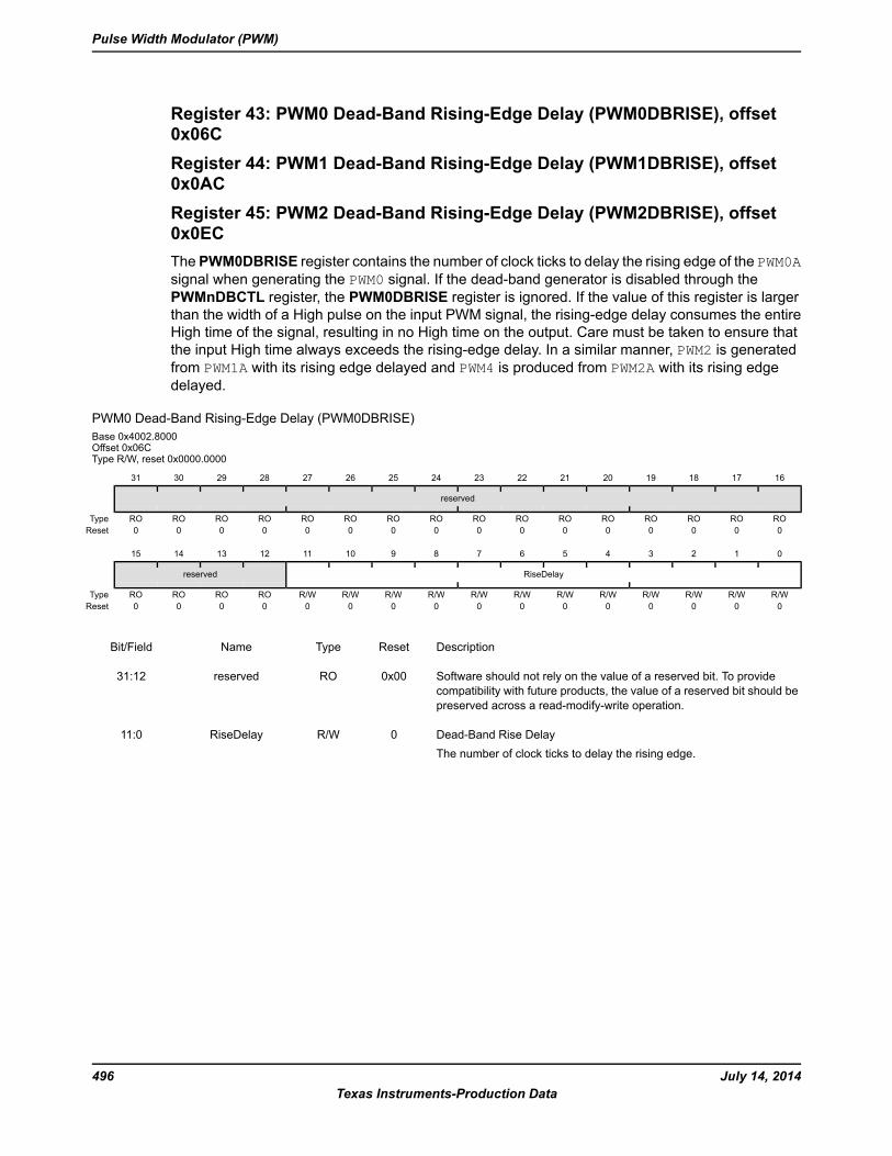
Register 43: PWM0 Dead-Band Rising-Edge Delay (PWM0DBRISE), offset0x06CRegister 44: PWM1 Dead-Band Rising-Edge Delay (PWM1DBRISE), offset0x0ACRegister 45: PWM2 Dead-Band Rising-Edge Delay (PWM2DBRISE), offset0x0ECThe PWM0DBRISE register contains the number of clock ticks to delay the rising edge of the PWM0Asignal when generating the PWM0 signal. If the dead-band generator is disabled through thePWMnDBCTL register, the PWM0DBRISE register is ignored. If the value of this register is largerthan the width of a High pulse on the input PWM signal, the rising-edge delay consumes the entireHigh time of the signal, resulting in no High time on the output. Care must be taken to ensure thatthe input High time always exceeds the rising-edge delay. In a similar manner, PWM2 is generatedfrom PWM1A with its rising edge delayed and PWM4 is produced from PWM2A with its rising edgedelayed.
PWM0 Dead-Band Rising-Edge Delay (PWM0DBRISE)Base 0x4002.8000Offset 0x06CType R/W, reset 0x0000.0000
16171819202122232425262728293031
reserved
ROROROROROROROROROROROROROROROROType0000000000000000Reset
0123456789101112131415
RiseDelayreserved
R/WR/WR/WR/WR/WR/WR/WR/WR/WR/WR/WR/WROROROROType0000000000000000Reset
DescriptionResetTypeNameBit/Field
Software should not rely on the value of a reserved bit. To providecompatibility with future products, the value of a reserved bit should bepreserved across a read-modify-write operation.
0x00ROreserved31:12
Dead-Band Rise DelayThe number of clock ticks to delay the rising edge.
0R/WRiseDelay11:0
July 14, 2014496Texas Instruments-Production Data
Pulse Width Modulator (PWM)
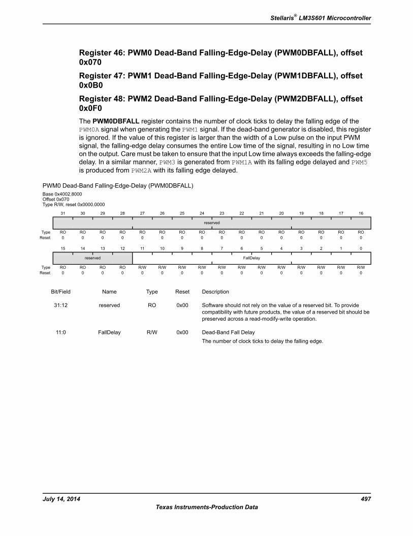
Register 46: PWM0 Dead-Band Falling-Edge-Delay (PWM0DBFALL), offset0x070Register 47: PWM1 Dead-Band Falling-Edge-Delay (PWM1DBFALL), offset0x0B0Register 48: PWM2 Dead-Band Falling-Edge-Delay (PWM2DBFALL), offset0x0F0The PWM0DBFALL register contains the number of clock ticks to delay the falling edge of thePWM0A signal when generating the PWM1 signal. If the dead-band generator is disabled, this registeris ignored. If the value of this register is larger than the width of a Low pulse on the input PWMsignal, the falling-edge delay consumes the entire Low time of the signal, resulting in no Low timeon the output. Care must be taken to ensure that the input Low time always exceeds the falling-edgedelay. In a similar manner, PWM3 is generated from PWM1A with its falling edge delayed and PWM5is produced from PWM2A with its falling edge delayed.
PWM0 Dead-Band Falling-Edge-Delay (PWM0DBFALL)Base 0x4002.8000Offset 0x070Type R/W, reset 0x0000.0000
16171819202122232425262728293031
reserved
ROROROROROROROROROROROROROROROROType0000000000000000Reset
0123456789101112131415
FallDelayreserved
R/WR/WR/WR/WR/WR/WR/WR/WR/WR/WR/WR/WROROROROType0000000000000000Reset
DescriptionResetTypeNameBit/Field
Software should not rely on the value of a reserved bit. To providecompatibility with future products, the value of a reserved bit should bepreserved across a read-modify-write operation.
0x00ROreserved31:12
Dead-Band Fall DelayThe number of clock ticks to delay the falling edge.
0x00R/WFallDelay11:0
497July 14, 2014Texas Instruments-Production Data
Stellaris® LM3S601 Microcontroller
15 Quadrature Encoder Interface (QEI)A quadrature encoder, also known as a 2-channel incremental encoder, converts linear displacementinto a pulse signal. By monitoring both the number of pulses and the relative phase of the two signals,you can track the position, direction of rotation, and speed. In addition, a third channel, or indexsignal, can be used to reset the position counter.
The Stellaris® quadrature encoder interface (QEI) module interprets the code produced by aquadrature encoder wheel to integrate position over time and determine direction of rotation. Inaddition, it can capture a running estimate of the velocity of the encoder wheel.
The Stellaris quadrature encoder has the following features:
Position integrator that tracks the encoder position
Velocity capture using built-in timer
The input frequency of the QEI inputs may be as high as 1/4 of the processor frequency (forexample, 12.5 MHz for a 50-MHz system)
Interrupt generation on:
– Index pulse
– Velocity-timer expiration
– Direction change
– Quadrature error detection
15.1 Block DiagramFigure 15-1 on page 499 provides a block diagram of a Stellaris QEI module.
July 14, 2014498Texas Instruments-Production Data
Quadrature Encoder Interface (QEI)
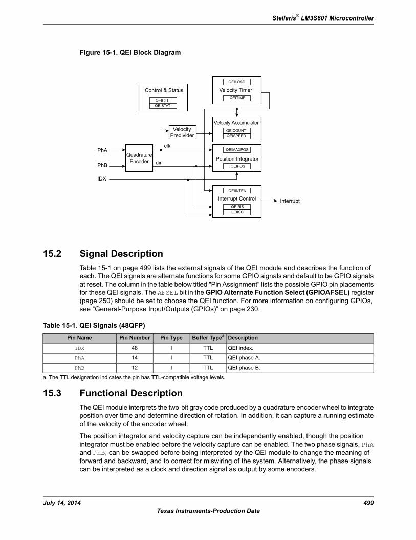
Figure 15-1. QEI Block Diagram
QuadratureEncoder
VelocityPredivider
Interrupt ControlQEIINTEN
QEIRISQEIISC
Position Integrator
QEIMAXPOS
QEIPOS
Velocity AccumulatorQEICOUNTQEISPEED
Velocity Timer
QEILOAD
QEITIME
PhA
PhB
IDX
clk
dir
Interrupt
Control & Status
QEICTLQEISTAT
15.2 Signal DescriptionTable 15-1 on page 499 lists the external signals of the QEI module and describes the function ofeach. The QEI signals are alternate functions for some GPIO signals and default to be GPIO signalsat reset. The column in the table below titled "Pin Assignment" lists the possible GPIO pin placementsfor these QEI signals. The AFSEL bit in theGPIO Alternate Function Select (GPIOAFSEL) register(page 250) should be set to choose the QEI function. For more information on configuring GPIOs,see “General-Purpose Input/Outputs (GPIOs)” on page 230.
Table 15-1. QEI Signals (48QFP)
DescriptionBuffer TypeaPin TypePin NumberPin Name
QEI index.TTLI48IDX
QEI phase A.TTLI14PhA
QEI phase B.TTLI12PhB
a. The TTL designation indicates the pin has TTL-compatible voltage levels.
15.3 Functional DescriptionTheQEI module interprets the two-bit gray code produced by a quadrature encoder wheel to integrateposition over time and determine direction of rotation. In addition, it can capture a running estimateof the velocity of the encoder wheel.
The position integrator and velocity capture can be independently enabled, though the positionintegrator must be enabled before the velocity capture can be enabled. The two phase signals, PhAand PhB, can be swapped before being interpreted by the QEI module to change the meaning offorward and backward, and to correct for miswiring of the system. Alternatively, the phase signalscan be interpreted as a clock and direction signal as output by some encoders.
499July 14, 2014Texas Instruments-Production Data
Stellaris® LM3S601 Microcontroller
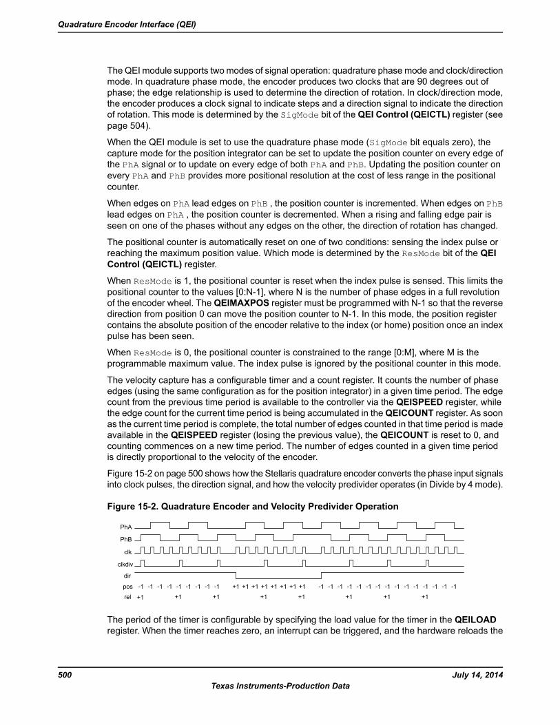
The QEI module supports twomodes of signal operation: quadrature phasemode and clock/directionmode. In quadrature phase mode, the encoder produces two clocks that are 90 degrees out ofphase; the edge relationship is used to determine the direction of rotation. In clock/direction mode,the encoder produces a clock signal to indicate steps and a direction signal to indicate the directionof rotation. This mode is determined by the SigMode bit of the QEI Control (QEICTL) register (seepage 504).
When the QEI module is set to use the quadrature phase mode (SigMode bit equals zero), thecapture mode for the position integrator can be set to update the position counter on every edge ofthe PhA signal or to update on every edge of both PhA and PhB. Updating the position counter onevery PhA and PhB provides more positional resolution at the cost of less range in the positionalcounter.
When edges on PhA lead edges on PhB , the position counter is incremented. When edges on PhBlead edges on PhA , the position counter is decremented. When a rising and falling edge pair isseen on one of the phases without any edges on the other, the direction of rotation has changed.
The positional counter is automatically reset on one of two conditions: sensing the index pulse orreaching the maximum position value. Which mode is determined by the ResMode bit of the QEIControl (QEICTL) register.
When ResMode is 1, the positional counter is reset when the index pulse is sensed. This limits thepositional counter to the values [0:N-1], where N is the number of phase edges in a full revolutionof the encoder wheel. The QEIMAXPOS register must be programmed with N-1 so that the reversedirection from position 0 can move the position counter to N-1. In this mode, the position registercontains the absolute position of the encoder relative to the index (or home) position once an indexpulse has been seen.
When ResMode is 0, the positional counter is constrained to the range [0:M], where M is theprogrammable maximum value. The index pulse is ignored by the positional counter in this mode.
The velocity capture has a configurable timer and a count register. It counts the number of phaseedges (using the same configuration as for the position integrator) in a given time period. The edgecount from the previous time period is available to the controller via the QEISPEED register, whilethe edge count for the current time period is being accumulated in theQEICOUNT register. As soonas the current time period is complete, the total number of edges counted in that time period is madeavailable in the QEISPEED register (losing the previous value), the QEICOUNT is reset to 0, andcounting commences on a new time period. The number of edges counted in a given time periodis directly proportional to the velocity of the encoder.
Figure 15-2 on page 500 shows how the Stellaris quadrature encoder converts the phase input signalsinto clock pulses, the direction signal, and how the velocity predivider operates (in Divide by 4 mode).
Figure 15-2. Quadrature Encoder and Velocity Predivider Operation
PhB
clk
clkdiv
dir
-1 -1 -1 -1 -1 -1 -1 -1 -1 +1 +1 +1 +1 +1 +1 +1 +1 -1 -1 -1 -1 -1 -1 -1 -1 -1 -1 -1 -1 -1 -1 -1pos
PhA
+1 +1 +1 +1 +1 +1 +1 +1rel
The period of the timer is configurable by specifying the load value for the timer in the QEILOADregister. When the timer reaches zero, an interrupt can be triggered, and the hardware reloads the
July 14, 2014500Texas Instruments-Production Data
Quadrature Encoder Interface (QEI)
timer with the QEILOAD value and continues to count down. At lower encoder speeds, a longertimer period is needed to be able to capture enough edges to have a meaningful result. At higherencoder speeds, both a shorter timer period and/or the velocity predivider can be used.
The following equation converts the velocity counter value into an rpm value:
rpm = (clock * (2 ^ VelDiv) * Speed * 60) ÷ (Load * ppr * edges)
where:
clock is the controller clock rate
ppr is the number of pulses per revolution of the physical encoder
edges is 2 or 4, based on the capture mode set in the QEICTL register (2 for CapMode set to 0 and4 for CapMode set to 1)
For example, consider a motor running at 600 rpm. A 2048 pulse per revolution quadrature encoderis attached to the motor, producing 8192 phase edges per revolution. With a velocity predivider of÷1 (VelDiv set to 0) and clocking on both PhA and PhB edges, this results in 81,920 pulses persecond (the motor turns 10 times per second). If the timer were clocked at 10,000 Hz, and the loadvalue was 2,500 (¼ of a second), it would count 20,480 pulses per update. Using the above equation:
rpm = (10000 * 1 * 20480 * 60) ÷ (2500 * 2048 * 4) = 600 rpm
Now, consider that the motor is sped up to 3000 rpm. This results in 409,600 pulses per second,or 102,400 every ¼ of a second. Again, the above equation gives:
rpm = (10000 * 1 * 102400 * 60) ÷ (2500 * 2048 * 4) = 3000 rpm
Caremust be taken when evaluating this equation since intermediate valuesmay exceed the capacityof a 32-bit integer. In the above examples, the clock is 10,000 and the divider is 2,500; both couldbe predivided by 100 (at compile time if they are constants) and therefore be 100 and 25. In fact, ifthey were compile-time constants, they could also be reduced to a simple multiply by 4, cancelledby the ÷4 for the edge-count factor.
Important: Reducing constant factors at compile time is the best way to control the intermediatevalues of this equation, as well as reducing the processing requirement of computingthis equation.
The division can be avoided by selecting a timer load value such that the divisor is a power of 2; asimple shift can therefore be done in place of the division. For encoders with a power of 2 pulsesper revolution, this is a simple matter of selecting a power of 2 load value. For other encoders, aload value must be selected such that the product is very close to a power of two. For example, a100 pulse per revolution encoder could use a load value of 82, resulting in 32,800 as the divisor,which is 0.09% above 214; in this case a shift by 15 would be an adequate approximation of thedivide in most cases. If absolute accuracy were required, the controller’s divide instruction could beused.
The QEI module can produce a controller interrupt on several events: phase error, direction change,reception of the index pulse, and expiration of the velocity timer. Standard masking, raw interruptstatus, interrupt status, and interrupt clear capabilities are provided.
15.4 Initialization and ConfigurationThe following example shows how to configure the Quadrature Encoder module to read back anabsolute position:
501July 14, 2014Texas Instruments-Production Data
Stellaris® LM3S601 Microcontroller
1. Enable the QEI clock by writing a value of 0x0000.0100 to the RCGC1 register in the SystemControl module.
2. Enable the clock to the appropriate GPIO module via the RCGC2 register in the System Controlmodule.
3. In the GPIO module, enable the appropriate pins for their alternate function using theGPIOAFSEL register.
4. Configure the quadrature encoder to capture edges on both signals and maintain an absoluteposition by resetting on index pulses. Using a 1000-line encoder at four edges per line, thereare 4000 pulses per revolution; therefore, set the maximum position to 3999 (0xF9F) since thecount is zero-based.
Write the QEICTL register with the value of 0x0000.0018.
Write the QEIMAXPOS register with the value of 0x0000.0F9F.
5. Enable the quadrature encoder by setting bit 0 of the QEICTL register.
6. Delay for some time.
7. Read the encoder position by reading the QEIPOS register value.
15.5 Register MapTable 15-2 on page 502 lists the QEI registers. The offset listed is a hexadecimal increment to theregister’s address, relative to the module’s base address:
QEI0: 0x4002.C000
Note that the QEI module clock must be enabled before the registers can be programmed (seepage 194). There must be a delay of 3 system clocks after the QEI module clock is enabled beforeany QEI module registers are accessed.
Table 15-2. QEI Register Map
SeepageDescriptionResetTypeNameOffset
504QEI Control0x0000.0000R/WQEICTL0x000
506QEI Status0x0000.0000ROQEISTAT0x004
507QEI Position0x0000.0000R/WQEIPOS0x008
508QEI Maximum Position0x0000.0000R/WQEIMAXPOS0x00C
509QEI Timer Load0x0000.0000R/WQEILOAD0x010
510QEI Timer0x0000.0000ROQEITIME0x014
511QEI Velocity Counter0x0000.0000ROQEICOUNT0x018
512QEI Velocity0x0000.0000ROQEISPEED0x01C
513QEI Interrupt Enable0x0000.0000R/WQEIINTEN0x020
514QEI Raw Interrupt Status0x0000.0000ROQEIRIS0x024
July 14, 2014502Texas Instruments-Production Data
Quadrature Encoder Interface (QEI)
Table 15-2. QEI Register Map (continued)
SeepageDescriptionResetTypeNameOffset
515QEI Interrupt Status and Clear0x0000.0000R/W1CQEIISC0x028
15.6 Register DescriptionsThe remainder of this section lists and describes the QEI registers, in numerical order by addressoffset.
503July 14, 2014Texas Instruments-Production Data
Stellaris® LM3S601 Microcontroller
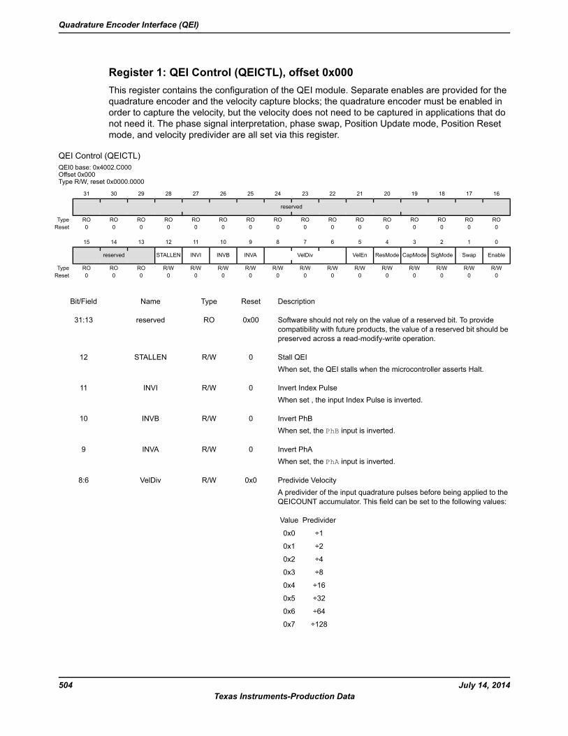
Register 1: QEI Control (QEICTL), offset 0x000This register contains the configuration of the QEI module. Separate enables are provided for thequadrature encoder and the velocity capture blocks; the quadrature encoder must be enabled inorder to capture the velocity, but the velocity does not need to be captured in applications that donot need it. The phase signal interpretation, phase swap, Position Update mode, Position Resetmode, and velocity predivider are all set via this register.
QEI Control (QEICTL)QEI0 base: 0x4002.C000Offset 0x000Type R/W, reset 0x0000.0000
16171819202122232425262728293031
reserved
ROROROROROROROROROROROROROROROROType0000000000000000Reset
0123456789101112131415
EnableSwapSigModeCapModeResModeVelEnVelDivINVAINVBINVISTALLENreserved
R/WR/WR/WR/WR/WR/WR/WR/WR/WR/WR/WR/WR/WROROROType0000000000000000Reset
DescriptionResetTypeNameBit/Field
Software should not rely on the value of a reserved bit. To providecompatibility with future products, the value of a reserved bit should bepreserved across a read-modify-write operation.
0x00ROreserved31:13
Stall QEIWhen set, the QEI stalls when the microcontroller asserts Halt.
0R/WSTALLEN12
Invert Index PulseWhen set , the input Index Pulse is inverted.
0R/WINVI11
Invert PhBWhen set, the PhB input is inverted.
0R/WINVB10
Invert PhAWhen set, the PhA input is inverted.
0R/WINVA9
Predivide VelocityA predivider of the input quadrature pulses before being applied to theQEICOUNT accumulator. This field can be set to the following values:
PredividerValue
÷10x0
÷20x1
÷40x2
÷80x3
÷160x4
÷320x5
÷640x6
÷1280x7
0x0R/WVelDiv8:6
July 14, 2014504Texas Instruments-Production Data
Quadrature Encoder Interface (QEI)
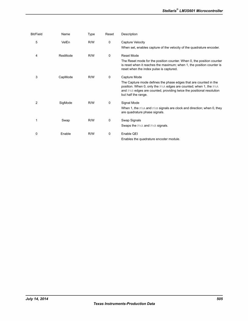
DescriptionResetTypeNameBit/Field
Capture VelocityWhen set, enables capture of the velocity of the quadrature encoder.
0R/WVelEn5
Reset ModeThe Reset mode for the position counter. When 0, the position counteris reset when it reaches the maximum; when 1, the position counter isreset when the index pulse is captured.
0R/WResMode4
Capture ModeThe Capture mode defines the phase edges that are counted in theposition. When 0, only the PhA edges are counted; when 1, the PhAand PhB edges are counted, providing twice the positional resolutionbut half the range.
0R/WCapMode3
Signal ModeWhen 1, the PhA and PhB signals are clock and direction; when 0, theyare quadrature phase signals.
0R/WSigMode2
Swap SignalsSwaps the PhA and PhB signals.
0R/WSwap1
Enable QEIEnables the quadrature encoder module.
0R/WEnable0
505July 14, 2014Texas Instruments-Production Data
Stellaris® LM3S601 Microcontroller
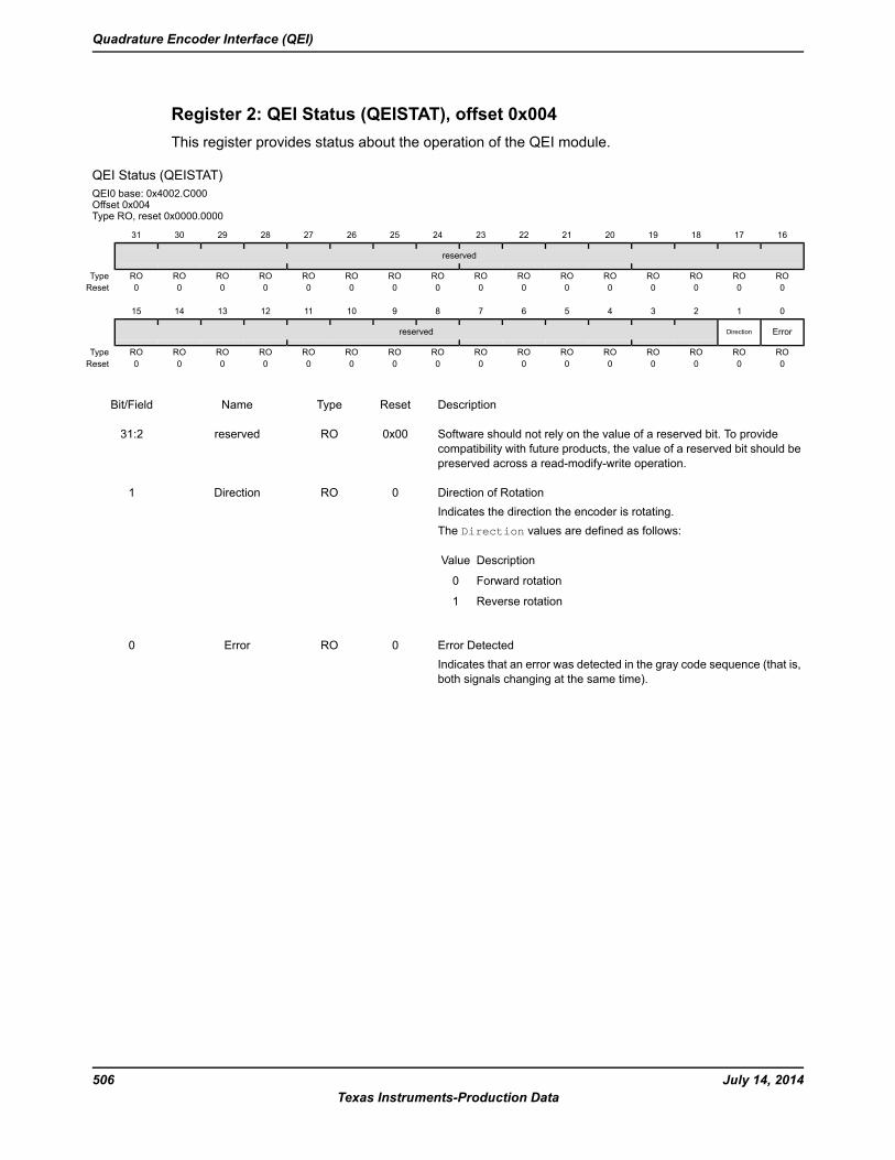
Register 2: QEI Status (QEISTAT), offset 0x004This register provides status about the operation of the QEI module.
QEI Status (QEISTAT)QEI0 base: 0x4002.C000Offset 0x004Type RO, reset 0x0000.0000
16171819202122232425262728293031
reserved
ROROROROROROROROROROROROROROROROType0000000000000000Reset
0123456789101112131415
ErrorDirectionreserved
ROROROROROROROROROROROROROROROROType0000000000000000Reset
DescriptionResetTypeNameBit/Field
Software should not rely on the value of a reserved bit. To providecompatibility with future products, the value of a reserved bit should bepreserved across a read-modify-write operation.
0x00ROreserved31:2
Direction of RotationIndicates the direction the encoder is rotating.The Direction values are defined as follows:
DescriptionValue
Forward rotation0
Reverse rotation1
0RODirection1
Error DetectedIndicates that an error was detected in the gray code sequence (that is,both signals changing at the same time).
0ROError0
July 14, 2014506Texas Instruments-Production Data
Quadrature Encoder Interface (QEI)
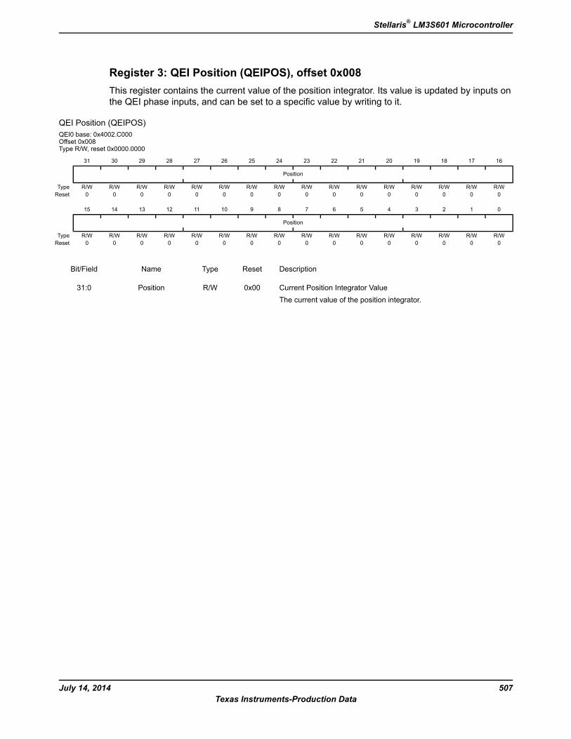
Register 3: QEI Position (QEIPOS), offset 0x008This register contains the current value of the position integrator. Its value is updated by inputs onthe QEI phase inputs, and can be set to a specific value by writing to it.
QEI Position (QEIPOS)QEI0 base: 0x4002.C000Offset 0x008Type R/W, reset 0x0000.0000
16171819202122232425262728293031
Position
R/WR/WR/WR/WR/WR/WR/WR/WR/WR/WR/WR/WR/WR/WR/WR/WType0000000000000000Reset
0123456789101112131415
Position
R/WR/WR/WR/WR/WR/WR/WR/WR/WR/WR/WR/WR/WR/WR/WR/WType0000000000000000Reset
DescriptionResetTypeNameBit/Field
Current Position Integrator ValueThe current value of the position integrator.
0x00R/WPosition31:0
507July 14, 2014Texas Instruments-Production Data
Stellaris® LM3S601 Microcontroller
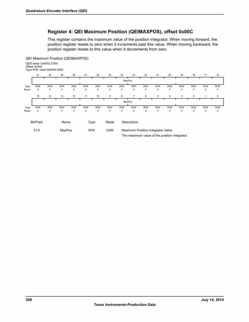
Register 4: QEI Maximum Position (QEIMAXPOS), offset 0x00CThis register contains the maximum value of the position integrator. When moving forward, theposition register resets to zero when it increments past this value. When moving backward, theposition register resets to this value when it decrements from zero.
QEI Maximum Position (QEIMAXPOS)QEI0 base: 0x4002.C000Offset 0x00CType R/W, reset 0x0000.0000
16171819202122232425262728293031
MaxPos
R/WR/WR/WR/WR/WR/WR/WR/WR/WR/WR/WR/WR/WR/WR/WR/WType0000000000000000Reset
0123456789101112131415
MaxPos
R/WR/WR/WR/WR/WR/WR/WR/WR/WR/WR/WR/WR/WR/WR/WR/WType0000000000000000Reset
DescriptionResetTypeNameBit/Field
Maximum Position Integrator ValueThe maximum value of the position integrator.
0x00R/WMaxPos31:0
July 14, 2014508Texas Instruments-Production Data
Quadrature Encoder Interface (QEI)
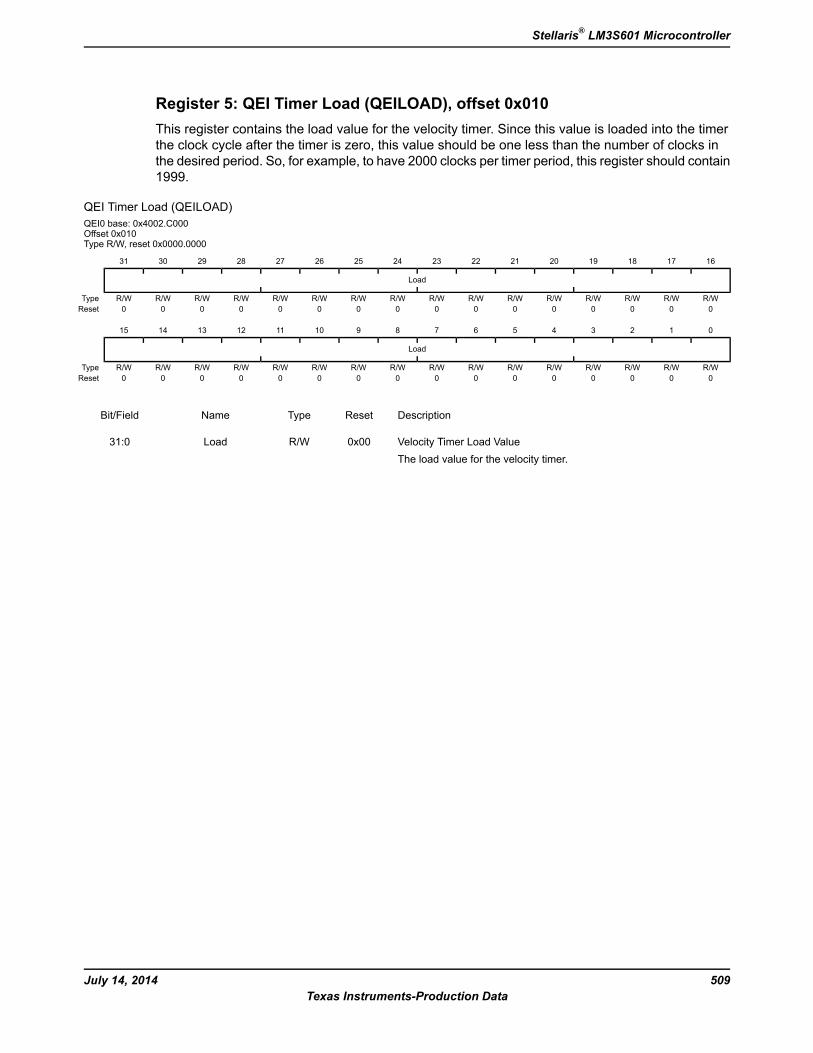
Register 5: QEI Timer Load (QEILOAD), offset 0x010This register contains the load value for the velocity timer. Since this value is loaded into the timerthe clock cycle after the timer is zero, this value should be one less than the number of clocks inthe desired period. So, for example, to have 2000 clocks per timer period, this register should contain1999.
QEI Timer Load (QEILOAD)QEI0 base: 0x4002.C000Offset 0x010Type R/W, reset 0x0000.0000
16171819202122232425262728293031
Load
R/WR/WR/WR/WR/WR/WR/WR/WR/WR/WR/WR/WR/WR/WR/WR/WType0000000000000000Reset
0123456789101112131415
Load
R/WR/WR/WR/WR/WR/WR/WR/WR/WR/WR/WR/WR/WR/WR/WR/WType0000000000000000Reset
DescriptionResetTypeNameBit/Field
Velocity Timer Load ValueThe load value for the velocity timer.
0x00R/WLoad31:0
509July 14, 2014Texas Instruments-Production Data
Stellaris® LM3S601 Microcontroller
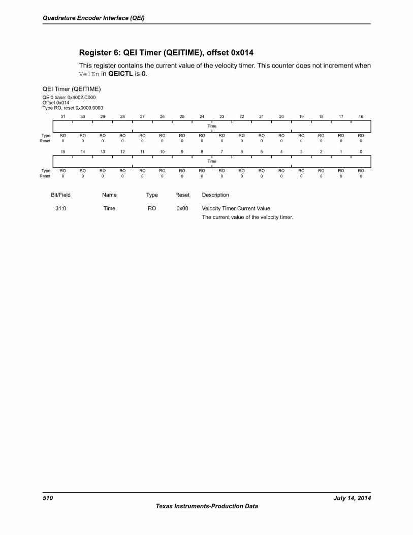
Register 6: QEI Timer (QEITIME), offset 0x014This register contains the current value of the velocity timer. This counter does not increment whenVelEn in QEICTL is 0.
QEI Timer (QEITIME)QEI0 base: 0x4002.C000Offset 0x014Type RO, reset 0x0000.0000
16171819202122232425262728293031
Time
ROROROROROROROROROROROROROROROROType0000000000000000Reset
0123456789101112131415
Time
ROROROROROROROROROROROROROROROROType0000000000000000Reset
DescriptionResetTypeNameBit/Field
Velocity Timer Current ValueThe current value of the velocity timer.
0x00ROTime31:0
July 14, 2014510Texas Instruments-Production Data
Quadrature Encoder Interface (QEI)
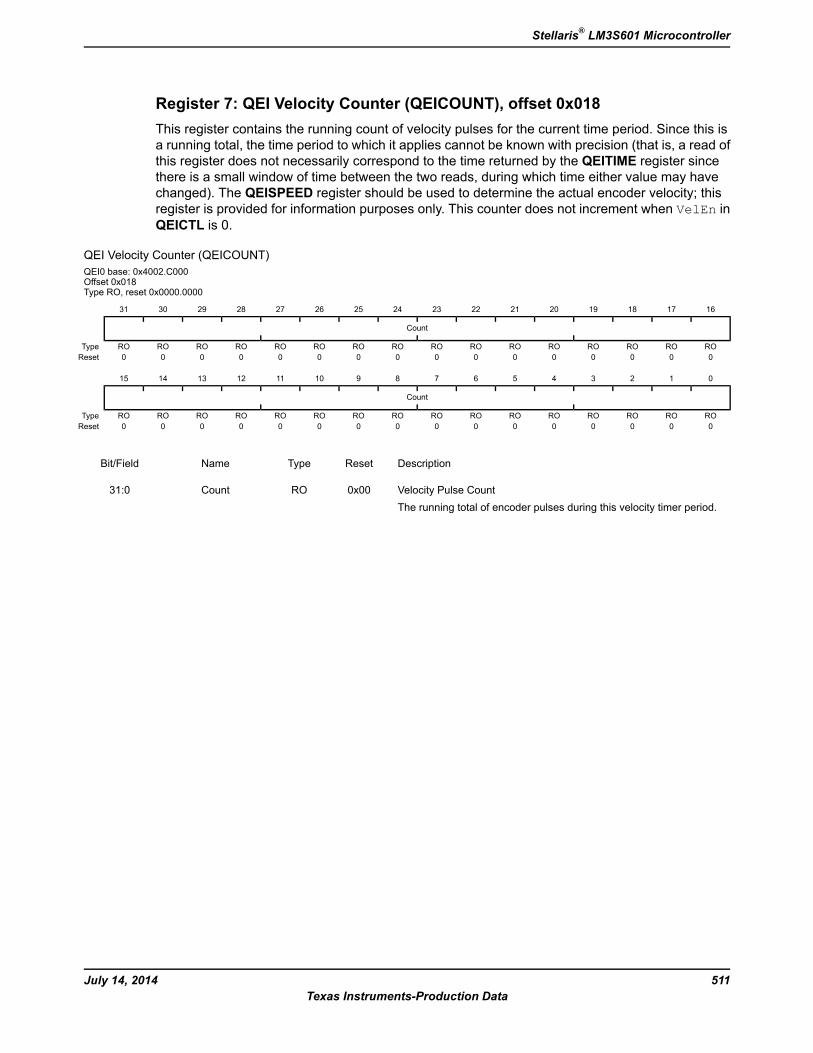
Register 7: QEI Velocity Counter (QEICOUNT), offset 0x018This register contains the running count of velocity pulses for the current time period. Since this isa running total, the time period to which it applies cannot be known with precision (that is, a read ofthis register does not necessarily correspond to the time returned by the QEITIME register sincethere is a small window of time between the two reads, during which time either value may havechanged). The QEISPEED register should be used to determine the actual encoder velocity; thisregister is provided for information purposes only. This counter does not increment when VelEn inQEICTL is 0.
QEI Velocity Counter (QEICOUNT)QEI0 base: 0x4002.C000Offset 0x018Type RO, reset 0x0000.0000
16171819202122232425262728293031
Count
ROROROROROROROROROROROROROROROROType0000000000000000Reset
0123456789101112131415
Count
ROROROROROROROROROROROROROROROROType0000000000000000Reset
DescriptionResetTypeNameBit/Field
Velocity Pulse CountThe running total of encoder pulses during this velocity timer period.
0x00ROCount31:0
511July 14, 2014Texas Instruments-Production Data
Stellaris® LM3S601 Microcontroller
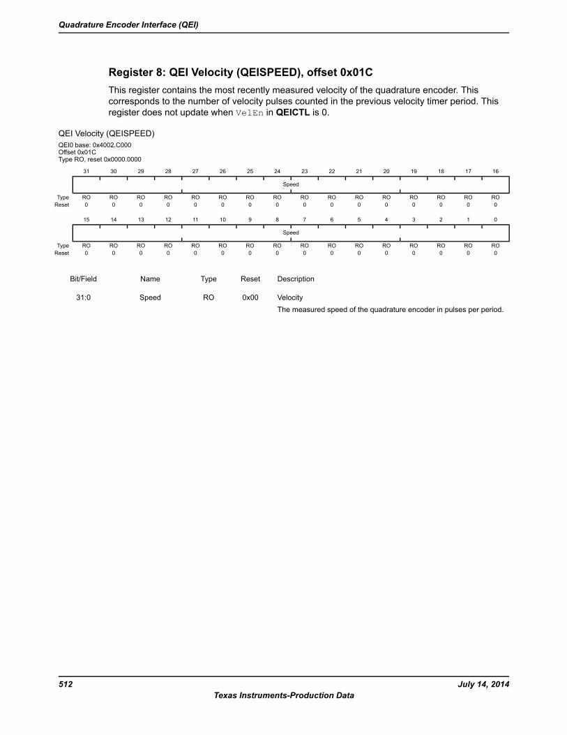
Register 8: QEI Velocity (QEISPEED), offset 0x01CThis register contains the most recently measured velocity of the quadrature encoder. Thiscorresponds to the number of velocity pulses counted in the previous velocity timer period. Thisregister does not update when VelEn in QEICTL is 0.
QEI Velocity (QEISPEED)QEI0 base: 0x4002.C000Offset 0x01CType RO, reset 0x0000.0000
16171819202122232425262728293031
Speed
ROROROROROROROROROROROROROROROROType0000000000000000Reset
0123456789101112131415
Speed
ROROROROROROROROROROROROROROROROType0000000000000000Reset
DescriptionResetTypeNameBit/Field
VelocityThe measured speed of the quadrature encoder in pulses per period.
0x00ROSpeed31:0
July 14, 2014512Texas Instruments-Production Data
Quadrature Encoder Interface (QEI)
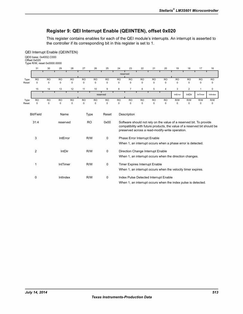
Register 9: QEI Interrupt Enable (QEIINTEN), offset 0x020This register contains enables for each of the QEI module’s interrupts. An interrupt is asserted tothe controller if its corresponding bit in this register is set to 1.
QEI Interrupt Enable (QEIINTEN)QEI0 base: 0x4002.C000Offset 0x020Type R/W, reset 0x0000.0000
16171819202122232425262728293031
reserved
ROROROROROROROROROROROROROROROROType0000000000000000Reset
0123456789101112131415
IntIndexIntTimerIntDirIntErrorreserved
R/WR/WR/WR/WROROROROROROROROROROROROType0000000000000000Reset
DescriptionResetTypeNameBit/Field
Software should not rely on the value of a reserved bit. To providecompatibility with future products, the value of a reserved bit should bepreserved across a read-modify-write operation.
0x00ROreserved31:4
Phase Error Interrupt EnableWhen 1, an interrupt occurs when a phase error is detected.
0R/WIntError3
Direction Change Interrupt EnableWhen 1, an interrupt occurs when the direction changes.
0R/WIntDir2
Timer Expires Interrupt EnableWhen 1, an interrupt occurs when the velocity timer expires.
0R/WIntTimer1
Index Pulse Detected Interrupt EnableWhen 1, an interrupt occurs when the index pulse is detected.
0R/WIntIndex0
513July 14, 2014Texas Instruments-Production Data
Stellaris® LM3S601 Microcontroller
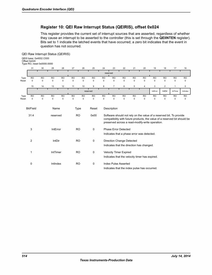
Register 10: QEI Raw Interrupt Status (QEIRIS), offset 0x024This register provides the current set of interrupt sources that are asserted, regardless of whetherthey cause an interrupt to be asserted to the controller (this is set through the QEIINTEN register).Bits set to 1 indicate the latched events that have occurred; a zero bit indicates that the event inquestion has not occurred.
QEI Raw Interrupt Status (QEIRIS)QEI0 base: 0x4002.C000Offset 0x024Type RO, reset 0x0000.0000
16171819202122232425262728293031
reserved
ROROROROROROROROROROROROROROROROType0000000000000000Reset
0123456789101112131415
IntIndexIntTimerIntDirIntErrorreserved
ROROROROROROROROROROROROROROROROType0000000000000000Reset
DescriptionResetTypeNameBit/Field
Software should not rely on the value of a reserved bit. To providecompatibility with future products, the value of a reserved bit should bepreserved across a read-modify-write operation.
0x00ROreserved31:4
Phase Error DetectedIndicates that a phase error was detected.
0ROIntError3
Direction Change DetectedIndicates that the direction has changed.
0ROIntDir2
Velocity Timer ExpiredIndicates that the velocity timer has expired.
0ROIntTimer1
Index Pulse AssertedIndicates that the index pulse has occurred.
0ROIntIndex0
July 14, 2014514Texas Instruments-Production Data
Quadrature Encoder Interface (QEI)
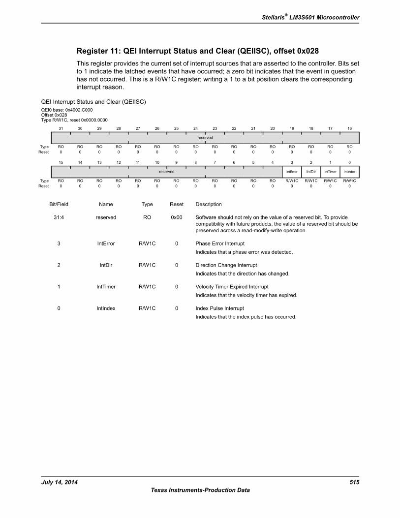
Register 11: QEI Interrupt Status and Clear (QEIISC), offset 0x028This register provides the current set of interrupt sources that are asserted to the controller. Bits setto 1 indicate the latched events that have occurred; a zero bit indicates that the event in questionhas not occurred. This is a R/W1C register; writing a 1 to a bit position clears the correspondinginterrupt reason.
QEI Interrupt Status and Clear (QEIISC)QEI0 base: 0x4002.C000Offset 0x028Type R/W1C, reset 0x0000.0000
16171819202122232425262728293031
reserved
ROROROROROROROROROROROROROROROROType0000000000000000Reset
0123456789101112131415
IntIndexIntTimerIntDirIntErrorreserved
R/W1CR/W1CR/W1CR/W1CROROROROROROROROROROROROType0000000000000000Reset
DescriptionResetTypeNameBit/Field
Software should not rely on the value of a reserved bit. To providecompatibility with future products, the value of a reserved bit should bepreserved across a read-modify-write operation.
0x00ROreserved31:4
Phase Error InterruptIndicates that a phase error was detected.
0R/W1CIntError3
Direction Change InterruptIndicates that the direction has changed.
0R/W1CIntDir2
Velocity Timer Expired InterruptIndicates that the velocity timer has expired.
0R/W1CIntTimer1
Index Pulse InterruptIndicates that the index pulse has occurred.
0R/W1CIntIndex0
515July 14, 2014Texas Instruments-Production Data
Stellaris® LM3S601 Microcontroller
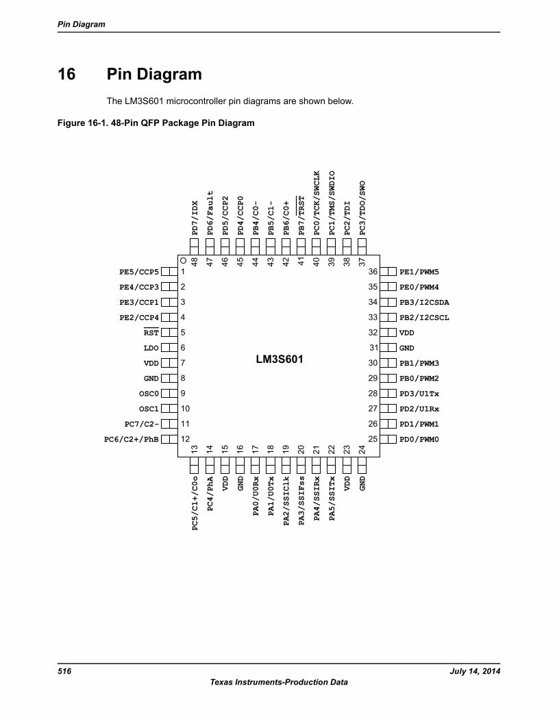
16 Pin DiagramThe LM3S601 microcontroller pin diagrams are shown below.
Figure 16-1. 48-Pin QFP Package Pin Diagram
July 14, 2014516Texas Instruments-Production Data
Pin Diagram
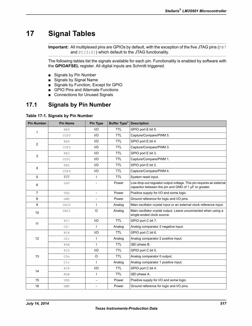
17 Signal TablesImportant: All multiplexed pins are GPIOs by default, with the exception of the five JTAG pins (PB7
and PC[3:0]) which default to the JTAG functionality.
The following tables list the signals available for each pin. Functionality is enabled by software withthe GPIOAFSEL register. All digital inputs are Schmitt triggered.
Signals by Pin Number Signals by Signal Name Signals by Function, Except for GPIO GPIO Pins and Alternate Functions Connections for Unused Signals
17.1 Signals by Pin Number
Table 17-1. Signals by Pin Number
DescriptionBuffer TypeaPin TypePin NamePin Number
GPIO port E bit 5.TTLI/OPE51
Capture/Compare/PWM 5.TTLI/OCCP5
GPIO port E bit 4.TTLI/OPE42
Capture/Compare/PWM 3.TTLI/OCCP3
GPIO port E bit 3.TTLI/OPE33
Capture/Compare/PWM 1.TTLI/OCCP1
GPIO port E bit 2.TTLI/OPE24
Capture/Compare/PWM 4.TTLI/OCCP4
System reset input.TTLIRST5
Low drop-out regulator output voltage. This pin requires an externalcapacitor between the pin and GND of 1 µF or greater.
Power-LDO6
Positive supply for I/O and some logic.Power-VDD7
Ground reference for logic and I/O pins.Power-GND8
Main oscillator crystal input or an external clock reference input.AnalogIOSC09
Main oscillator crystal output. Leave unconnected when using asingle-ended clock source.
AnalogOOSC110
GPIO port C bit 7.TTLI/OPC711
Analog comparator 2 negative input.AnalogIC2-
GPIO port C bit 6.TTLI/OPC6
12 Analog comparator 2 positive input.AnalogIC2+
QEI phase B.TTLIPhB
GPIO port C bit 5.TTLI/OPC5
13 Analog comparator 0 output.TTLOC0o
Analog comparator 1 positive input.AnalogIC1+
GPIO port C bit 4.TTLI/OPC414
QEI phase A.TTLIPhA
Positive supply for I/O and some logic.Power-VDD15
Ground reference for logic and I/O pins.Power-GND16
517July 14, 2014Texas Instruments-Production Data
Stellaris® LM3S601 Microcontroller
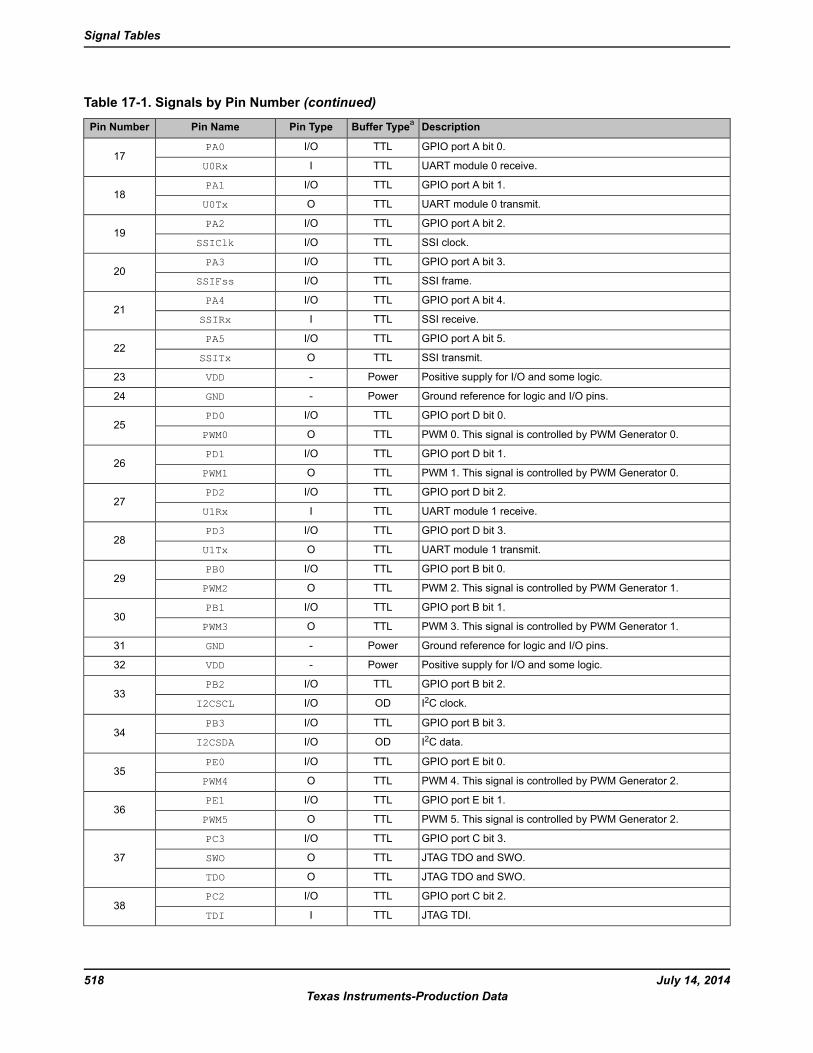
Table 17-1. Signals by Pin Number (continued)
DescriptionBuffer TypeaPin TypePin NamePin Number
GPIO port A bit 0.TTLI/OPA017
UART module 0 receive.TTLIU0Rx
GPIO port A bit 1.TTLI/OPA118
UART module 0 transmit.TTLOU0Tx
GPIO port A bit 2.TTLI/OPA219
SSI clock.TTLI/OSSIClk
GPIO port A bit 3.TTLI/OPA320
SSI frame.TTLI/OSSIFss
GPIO port A bit 4.TTLI/OPA421
SSI receive.TTLISSIRx
GPIO port A bit 5.TTLI/OPA522
SSI transmit.TTLOSSITx
Positive supply for I/O and some logic.Power-VDD23
Ground reference for logic and I/O pins.Power-GND24
GPIO port D bit 0.TTLI/OPD025
PWM 0. This signal is controlled by PWM Generator 0.TTLOPWM0
GPIO port D bit 1.TTLI/OPD126
PWM 1. This signal is controlled by PWM Generator 0.TTLOPWM1
GPIO port D bit 2.TTLI/OPD227
UART module 1 receive.TTLIU1Rx
GPIO port D bit 3.TTLI/OPD328
UART module 1 transmit.TTLOU1Tx
GPIO port B bit 0.TTLI/OPB029
PWM 2. This signal is controlled by PWM Generator 1.TTLOPWM2
GPIO port B bit 1.TTLI/OPB130
PWM 3. This signal is controlled by PWM Generator 1.TTLOPWM3
Ground reference for logic and I/O pins.Power-GND31
Positive supply for I/O and some logic.Power-VDD32
GPIO port B bit 2.TTLI/OPB233
I2C clock.ODI/OI2CSCL
GPIO port B bit 3.TTLI/OPB334
I2C data.ODI/OI2CSDA
GPIO port E bit 0.TTLI/OPE035
PWM 4. This signal is controlled by PWM Generator 2.TTLOPWM4
GPIO port E bit 1.TTLI/OPE136
PWM 5. This signal is controlled by PWM Generator 2.TTLOPWM5
GPIO port C bit 3.TTLI/OPC3
37 JTAG TDO and SWO.TTLOSWO
JTAG TDO and SWO.TTLOTDO
GPIO port C bit 2.TTLI/OPC238
JTAG TDI.TTLITDI
July 14, 2014518Texas Instruments-Production Data
Signal Tables
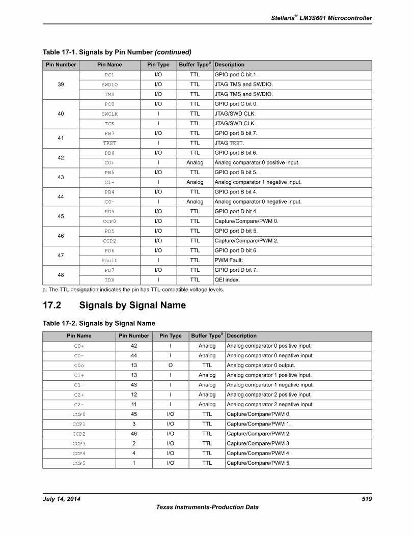
Table 17-1. Signals by Pin Number (continued)
DescriptionBuffer TypeaPin TypePin NamePin Number
GPIO port C bit 1.TTLI/OPC1
39 JTAG TMS and SWDIO.TTLI/OSWDIO
JTAG TMS and SWDIO.TTLI/OTMS
GPIO port C bit 0.TTLI/OPC0
40 JTAG/SWD CLK.TTLISWCLK
JTAG/SWD CLK.TTLITCK
GPIO port B bit 7.TTLI/OPB741
JTAG TRST.TTLITRST
GPIO port B bit 6.TTLI/OPB642
Analog comparator 0 positive input.AnalogIC0+
GPIO port B bit 5.TTLI/OPB543
Analog comparator 1 negative input.AnalogIC1-
GPIO port B bit 4.TTLI/OPB444
Analog comparator 0 negative input.AnalogIC0-
GPIO port D bit 4.TTLI/OPD445
Capture/Compare/PWM 0.TTLI/OCCP0
GPIO port D bit 5.TTLI/OPD546
Capture/Compare/PWM 2.TTLI/OCCP2
GPIO port D bit 6.TTLI/OPD647
PWM Fault.TTLIFault
GPIO port D bit 7.TTLI/OPD748
QEI index.TTLIIDX
a. The TTL designation indicates the pin has TTL-compatible voltage levels.
17.2 Signals by Signal Name
Table 17-2. Signals by Signal Name
DescriptionBuffer TypeaPin TypePin NumberPin Name
Analog comparator 0 positive input.AnalogI42C0+
Analog comparator 0 negative input.AnalogI44C0-
Analog comparator 0 output.TTLO13C0o
Analog comparator 1 positive input.AnalogI13C1+
Analog comparator 1 negative input.AnalogI43C1-
Analog comparator 2 positive input.AnalogI12C2+
Analog comparator 2 negative input.AnalogI11C2-
Capture/Compare/PWM 0.TTLI/O45CCP0
Capture/Compare/PWM 1.TTLI/O3CCP1
Capture/Compare/PWM 2.TTLI/O46CCP2
Capture/Compare/PWM 3.TTLI/O2CCP3
Capture/Compare/PWM 4.TTLI/O4CCP4
Capture/Compare/PWM 5.TTLI/O1CCP5
519July 14, 2014Texas Instruments-Production Data
Stellaris® LM3S601 Microcontroller
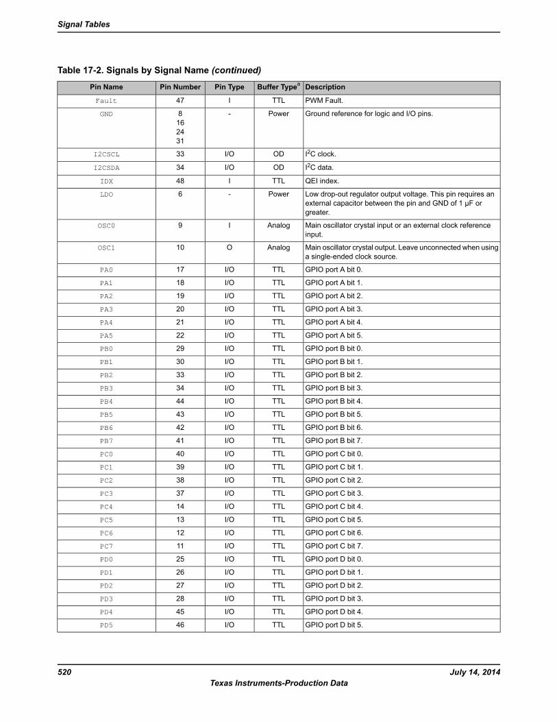
Table 17-2. Signals by Signal Name (continued)
DescriptionBuffer TypeaPin TypePin NumberPin Name
PWM Fault.TTLI47Fault
Ground reference for logic and I/O pins.Power-8162431
GND
I2C clock.ODI/O33I2CSCL
I2C data.ODI/O34I2CSDA
QEI index.TTLI48IDX
Low drop-out regulator output voltage. This pin requires anexternal capacitor between the pin and GND of 1 µF orgreater.
Power-6LDO
Main oscillator crystal input or an external clock referenceinput.
AnalogI9OSC0
Main oscillator crystal output. Leave unconnected when usinga single-ended clock source.
AnalogO10OSC1
GPIO port A bit 0.TTLI/O17PA0
GPIO port A bit 1.TTLI/O18PA1
GPIO port A bit 2.TTLI/O19PA2
GPIO port A bit 3.TTLI/O20PA3
GPIO port A bit 4.TTLI/O21PA4
GPIO port A bit 5.TTLI/O22PA5
GPIO port B bit 0.TTLI/O29PB0
GPIO port B bit 1.TTLI/O30PB1
GPIO port B bit 2.TTLI/O33PB2
GPIO port B bit 3.TTLI/O34PB3
GPIO port B bit 4.TTLI/O44PB4
GPIO port B bit 5.TTLI/O43PB5
GPIO port B bit 6.TTLI/O42PB6
GPIO port B bit 7.TTLI/O41PB7
GPIO port C bit 0.TTLI/O40PC0
GPIO port C bit 1.TTLI/O39PC1
GPIO port C bit 2.TTLI/O38PC2
GPIO port C bit 3.TTLI/O37PC3
GPIO port C bit 4.TTLI/O14PC4
GPIO port C bit 5.TTLI/O13PC5
GPIO port C bit 6.TTLI/O12PC6
GPIO port C bit 7.TTLI/O11PC7
GPIO port D bit 0.TTLI/O25PD0
GPIO port D bit 1.TTLI/O26PD1
GPIO port D bit 2.TTLI/O27PD2
GPIO port D bit 3.TTLI/O28PD3
GPIO port D bit 4.TTLI/O45PD4
GPIO port D bit 5.TTLI/O46PD5
July 14, 2014520Texas Instruments-Production Data
Signal Tables
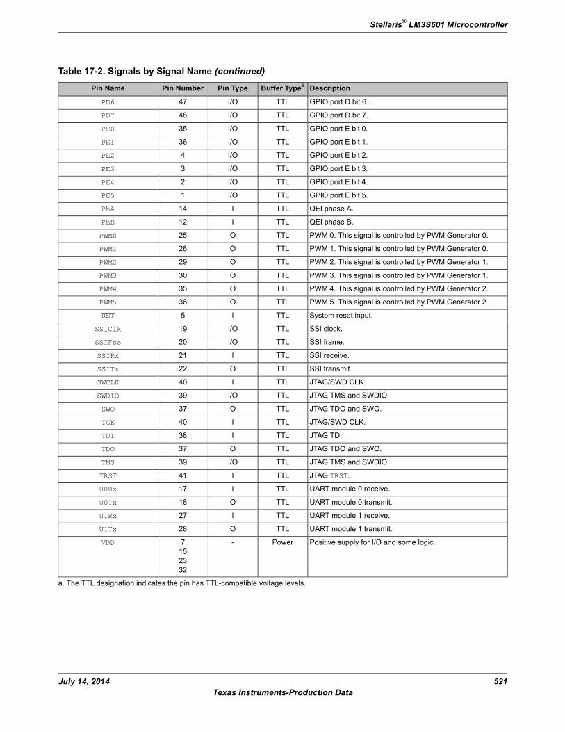
Table 17-2. Signals by Signal Name (continued)
DescriptionBuffer TypeaPin TypePin NumberPin Name
GPIO port D bit 6.TTLI/O47PD6
GPIO port D bit 7.TTLI/O48PD7
GPIO port E bit 0.TTLI/O35PE0
GPIO port E bit 1.TTLI/O36PE1
GPIO port E bit 2.TTLI/O4PE2
GPIO port E bit 3.TTLI/O3PE3
GPIO port E bit 4.TTLI/O2PE4
GPIO port E bit 5.TTLI/O1PE5
QEI phase A.TTLI14PhA
QEI phase B.TTLI12PhB
PWM 0. This signal is controlled by PWM Generator 0.TTLO25PWM0
PWM 1. This signal is controlled by PWM Generator 0.TTLO26PWM1
PWM 2. This signal is controlled by PWM Generator 1.TTLO29PWM2
PWM 3. This signal is controlled by PWM Generator 1.TTLO30PWM3
PWM 4. This signal is controlled by PWM Generator 2.TTLO35PWM4
PWM 5. This signal is controlled by PWM Generator 2.TTLO36PWM5
System reset input.TTLI5RST
SSI clock.TTLI/O19SSIClk
SSI frame.TTLI/O20SSIFss
SSI receive.TTLI21SSIRx
SSI transmit.TTLO22SSITx
JTAG/SWD CLK.TTLI40SWCLK
JTAG TMS and SWDIO.TTLI/O39SWDIO
JTAG TDO and SWO.TTLO37SWO
JTAG/SWD CLK.TTLI40TCK
JTAG TDI.TTLI38TDI
JTAG TDO and SWO.TTLO37TDO
JTAG TMS and SWDIO.TTLI/O39TMS
JTAG TRST.TTLI41TRST
UART module 0 receive.TTLI17U0Rx
UART module 0 transmit.TTLO18U0Tx
UART module 1 receive.TTLI27U1Rx
UART module 1 transmit.TTLO28U1Tx
Positive supply for I/O and some logic.Power-7152332
VDD
a. The TTL designation indicates the pin has TTL-compatible voltage levels.
521July 14, 2014Texas Instruments-Production Data
Stellaris® LM3S601 Microcontroller
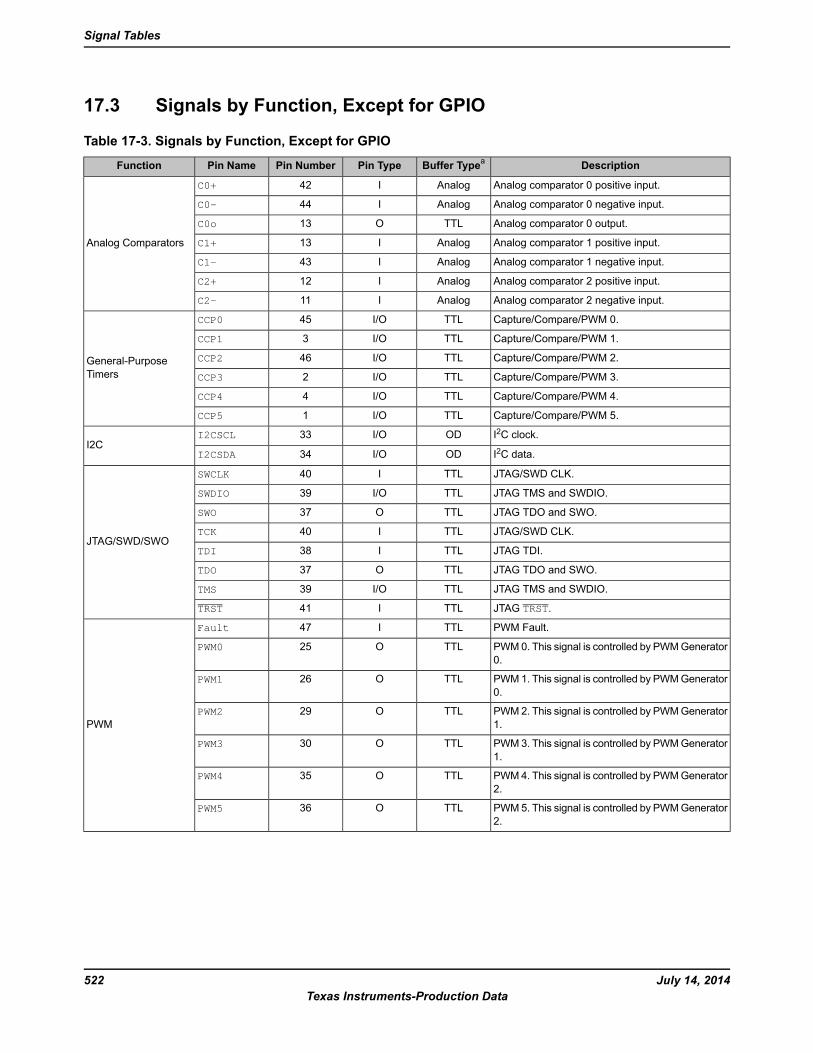
17.3 Signals by Function, Except for GPIO
Table 17-3. Signals by Function, Except for GPIO
DescriptionBuffer TypeaPin TypePin NumberPin NameFunction
Analog comparator 0 positive input.AnalogI42C0+
Analog Comparators
Analog comparator 0 negative input.AnalogI44C0-
Analog comparator 0 output.TTLO13C0o
Analog comparator 1 positive input.AnalogI13C1+
Analog comparator 1 negative input.AnalogI43C1-
Analog comparator 2 positive input.AnalogI12C2+
Analog comparator 2 negative input.AnalogI11C2-
Capture/Compare/PWM 0.TTLI/O45CCP0
General-PurposeTimers
Capture/Compare/PWM 1.TTLI/O3CCP1
Capture/Compare/PWM 2.TTLI/O46CCP2
Capture/Compare/PWM 3.TTLI/O2CCP3
Capture/Compare/PWM 4.TTLI/O4CCP4
Capture/Compare/PWM 5.TTLI/O1CCP5
I2C clock.ODI/O33I2CSCLI2C
I2C data.ODI/O34I2CSDA
JTAG/SWD CLK.TTLI40SWCLK
JTAG/SWD/SWO
JTAG TMS and SWDIO.TTLI/O39SWDIO
JTAG TDO and SWO.TTLO37SWO
JTAG/SWD CLK.TTLI40TCK
JTAG TDI.TTLI38TDI
JTAG TDO and SWO.TTLO37TDO
JTAG TMS and SWDIO.TTLI/O39TMS
JTAG TRST.TTLI41TRST
PWM Fault.TTLI47Fault
PWM
PWM0. This signal is controlled by PWMGenerator0.
TTLO25PWM0
PWM1. This signal is controlled by PWMGenerator0.
TTLO26PWM1
PWM2. This signal is controlled by PWMGenerator1.
TTLO29PWM2
PWM3. This signal is controlled by PWMGenerator1.
TTLO30PWM3
PWM4. This signal is controlled by PWMGenerator2.
TTLO35PWM4
PWM5. This signal is controlled by PWMGenerator2.
TTLO36PWM5
July 14, 2014522Texas Instruments-Production Data
Signal Tables
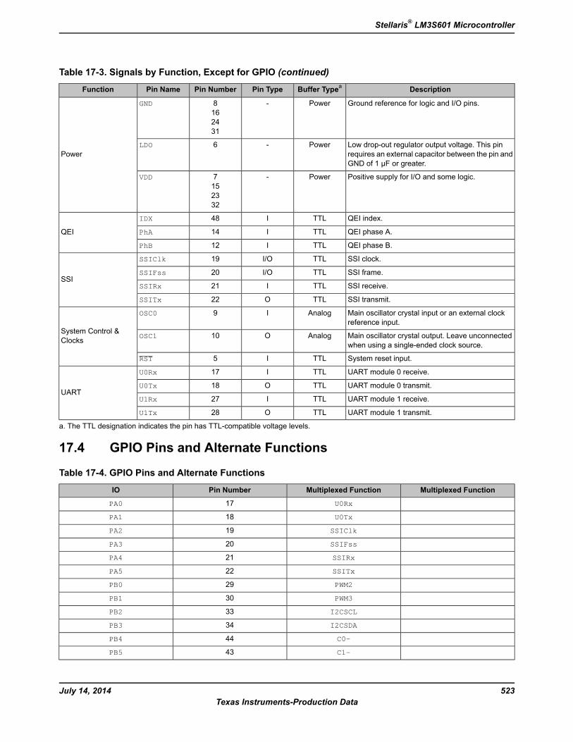
Table 17-3. Signals by Function, Except for GPIO (continued)
DescriptionBuffer TypeaPin TypePin NumberPin NameFunction
Ground reference for logic and I/O pins.Power-8162431
GND
PowerLow drop-out regulator output voltage. This pinrequires an external capacitor between the pin andGND of 1 µF or greater.
Power-6LDO
Positive supply for I/O and some logic.Power-7152332
VDD
QEI index.TTLI48IDX
QEI QEI phase A.TTLI14PhA
QEI phase B.TTLI12PhB
SSI clock.TTLI/O19SSIClk
SSISSI frame.TTLI/O20SSIFss
SSI receive.TTLI21SSIRx
SSI transmit.TTLO22SSITx
Main oscillator crystal input or an external clockreference input.
AnalogI9OSC0
System Control &Clocks Main oscillator crystal output. Leave unconnected
when using a single-ended clock source.AnalogO10OSC1
System reset input.TTLI5RST
UART module 0 receive.TTLI17U0Rx
UARTUART module 0 transmit.TTLO18U0Tx
UART module 1 receive.TTLI27U1Rx
UART module 1 transmit.TTLO28U1Tx
a. The TTL designation indicates the pin has TTL-compatible voltage levels.
17.4 GPIO Pins and Alternate Functions
Table 17-4. GPIO Pins and Alternate Functions
Multiplexed FunctionMultiplexed FunctionPin NumberIO
U0Rx17PA0
U0Tx18PA1
SSIClk19PA2
SSIFss20PA3
SSIRx21PA4
SSITx22PA5
PWM229PB0
PWM330PB1
I2CSCL33PB2
I2CSDA34PB3
C0-44PB4
C1-43PB5
523July 14, 2014Texas Instruments-Production Data
Stellaris® LM3S601 Microcontroller
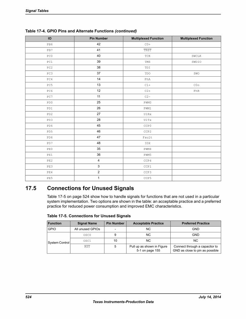
Table 17-4. GPIO Pins and Alternate Functions (continued)
Multiplexed FunctionMultiplexed FunctionPin NumberIO
C0+42PB6
TRST41PB7
SWCLKTCK40PC0
SWDIOTMS39PC1
TDI38PC2
SWOTDO37PC3
PhA14PC4
C0oC1+13PC5
PhBC2+12PC6
C2-11PC7
PWM025PD0
PWM126PD1
U1Rx27PD2
U1Tx28PD3
CCP045PD4
CCP246PD5
Fault47PD6
IDX48PD7
PWM435PE0
PWM536PE1
CCP44PE2
CCP13PE3
CCP32PE4
CCP51PE5
17.5 Connections for Unused SignalsTable 17-5 on page 524 show how to handle signals for functions that are not used in a particularsystem implementation. Two options are shown in the table: an acceptable practice and a preferredpractice for reduced power consumption and improved EMC characteristics.
Table 17-5. Connections for Unused Signals
Preferred PracticeAcceptable PracticePin NumberSignal NameFunction
GNDNC-All unused GPIOsGPIO
GNDNC9OSC0
SystemControl NCNC10OSC1
Connect through a capacitor toGND as close to pin as possible
Pull up as shown in Figure5-1 on page 155
5RST
July 14, 2014524Texas Instruments-Production Data
Signal Tables
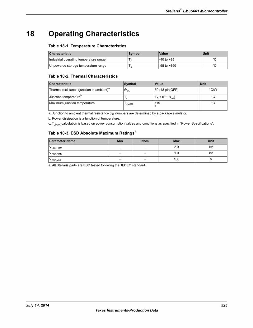
18 Operating CharacteristicsTable 18-1. Temperature Characteristics
UnitValueSymbolCharacteristic
°C-40 to +85TAIndustrial operating temperature range
°C-65 to +150TSUnpowered storage temperature range
Table 18-2. Thermal Characteristics
UnitValueSymbolCharacteristic
°C/W50 (48-pin QFP)ΘJAThermal resistance (junction to ambient)a
°CTA + (P • ΘJA)TJJunction temperatureb
°C115c
TJMAXMaximum junction temperature
a. Junction to ambient thermal resistance θJA numbers are determined by a package simulator.b. Power dissipation is a function of temperature.c. TJMAX calculation is based on power consumption values and conditions as specified in “Power Specifications”.
Table 18-3. ESD Absolute Maximum Ratingsa
UnitMaxNomMinParameter Name
kV2.0--VESDHBMkV1.0--VESDCDMV100--VESDMM
a. All Stellaris parts are ESD tested following the JEDEC standard.
525July 14, 2014Texas Instruments-Production Data
Stellaris® LM3S601 Microcontroller
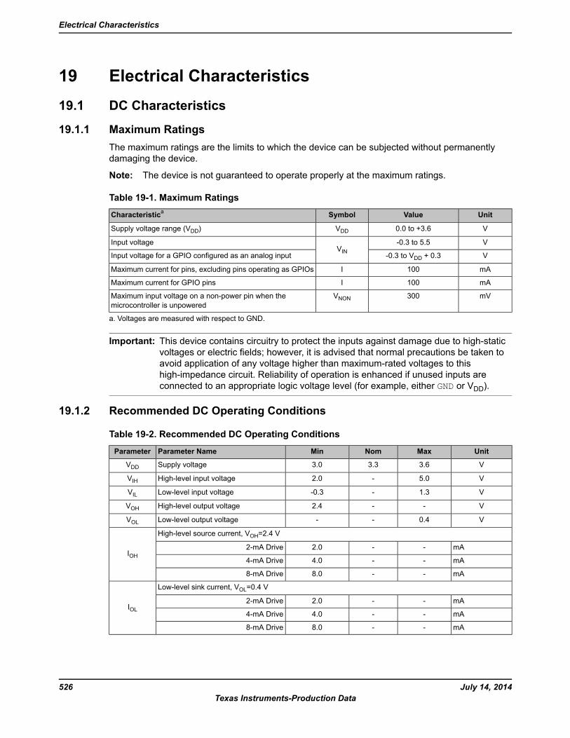
19 Electrical Characteristics19.1 DC Characteristics
19.1.1 Maximum RatingsThe maximum ratings are the limits to which the device can be subjected without permanentlydamaging the device.
Note: The device is not guaranteed to operate properly at the maximum ratings.
Table 19-1. Maximum Ratings
UnitValueSymbolCharacteristica
V0.0 to +3.6VDDSupply voltage range (VDD)
V-0.3 to 5.5VIN
Input voltage
V-0.3 to VDD + 0.3Input voltage for a GPIO configured as an analog input
mA100IMaximum current for pins, excluding pins operating as GPIOs
mA100IMaximum current for GPIO pins
mV300VNONMaximum input voltage on a non-power pin when themicrocontroller is unpowered
a. Voltages are measured with respect to GND.
Important: This device contains circuitry to protect the inputs against damage due to high-staticvoltages or electric fields; however, it is advised that normal precautions be taken toavoid application of any voltage higher than maximum-rated voltages to thishigh-impedance circuit. Reliability of operation is enhanced if unused inputs areconnected to an appropriate logic voltage level (for example, either GND or VDD).
19.1.2 Recommended DC Operating Conditions
Table 19-2. Recommended DC Operating Conditions
UnitMaxNomMinParameter NameParameter
V3.63.33.0Supply voltageVDDV5.0-2.0High-level input voltageVIHV1.3--0.3Low-level input voltageVILV--2.4High-level output voltageVOHV0.4--Low-level output voltageVOL
High-level source current, VOH=2.4 V
IOHmA--2.02-mA Drive
mA--4.04-mA Drive
mA--8.08-mA Drive
Low-level sink current, VOL=0.4 V
IOLmA--2.02-mA Drive
mA--4.04-mA Drive
mA--8.08-mA Drive
July 14, 2014526Texas Instruments-Production Data
Electrical Characteristics
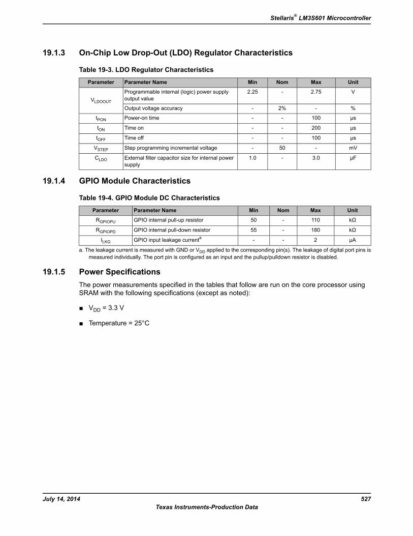
19.1.3 On-Chip Low Drop-Out (LDO) Regulator Characteristics
Table 19-3. LDO Regulator Characteristics
UnitMaxNomMinParameter NameParameter
V2.75-2.25Programmable internal (logic) power supplyoutput valueVLDOOUT
%-2%-Output voltage accuracy
µs100--Power-on timetPONµs200--Time ontONµs100--Time offtOFFmV-50-Step programming incremental voltageVSTEPµF3.0-1.0External filter capacitor size for internal power
supplyCLDO
19.1.4 GPIO Module Characteristics
Table 19-4. GPIO Module DC Characteristics
UnitMaxNomMinParameter NameParameter
kΩ110-50GPIO internal pull-up resistorRGPIOPU
kΩ180-55GPIO internal pull-down resistorRGPIOPD
µA2--GPIO input leakage currentaILKGa. The leakage current is measured with GND or VDD applied to the corresponding pin(s). The leakage of digital port pins is
measured individually. The port pin is configured as an input and the pullup/pulldown resistor is disabled.
19.1.5 Power SpecificationsThe power measurements specified in the tables that follow are run on the core processor usingSRAM with the following specifications (except as noted):
VDD = 3.3 V
Temperature = 25°C
527July 14, 2014Texas Instruments-Production Data
Stellaris® LM3S601 Microcontroller
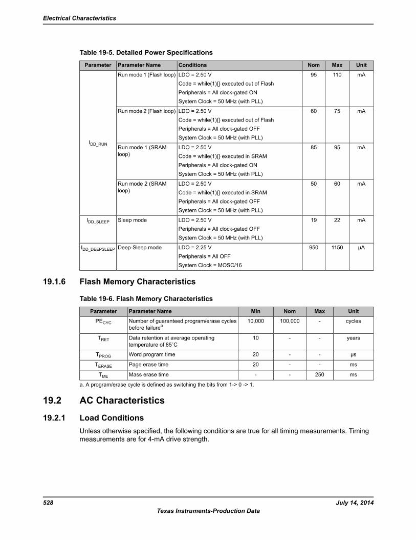
Table 19-5. Detailed Power Specifications
UnitMaxNomConditionsParameter NameParameter
mA11095LDO = 2.50 VCode = while(1) executed out of FlashPeripherals = All clock-gated ONSystem Clock = 50 MHz (with PLL)
Runmode 1 (Flash loop)
IDD_RUN
mA7560LDO = 2.50 VCode = while(1) executed out of FlashPeripherals = All clock-gated OFFSystem Clock = 50 MHz (with PLL)
Runmode 2 (Flash loop)
mA9585LDO = 2.50 VCode = while(1) executed in SRAMPeripherals = All clock-gated ONSystem Clock = 50 MHz (with PLL)
Run mode 1 (SRAMloop)
mA6050LDO = 2.50 VCode = while(1) executed in SRAMPeripherals = All clock-gated OFFSystem Clock = 50 MHz (with PLL)
Run mode 2 (SRAMloop)
mA2219LDO = 2.50 VPeripherals = All clock-gated OFFSystem Clock = 50 MHz (with PLL)
Sleep modeIDD_SLEEP
μA1150950LDO = 2.25 VPeripherals = All OFFSystem Clock = MOSC/16
Deep-Sleep modeIDD_DEEPSLEEP
19.1.6 Flash Memory Characteristics
Table 19-6. Flash Memory Characteristics
UnitMaxNomMinParameter NameParameter
cycles-100,00010,000Number of guaranteed program/erase cyclesbefore failurea
PECYC
years--10Data retention at average operatingtemperature of 85˚C
TRET
µs--20Word program timeTPROGms--20Page erase timeTERASEms250--Mass erase timeTME
a. A program/erase cycle is defined as switching the bits from 1-> 0 -> 1.
19.2 AC Characteristics
19.2.1 Load ConditionsUnless otherwise specified, the following conditions are true for all timing measurements. Timingmeasurements are for 4-mA drive strength.
July 14, 2014528Texas Instruments-Production Data
Electrical Characteristics
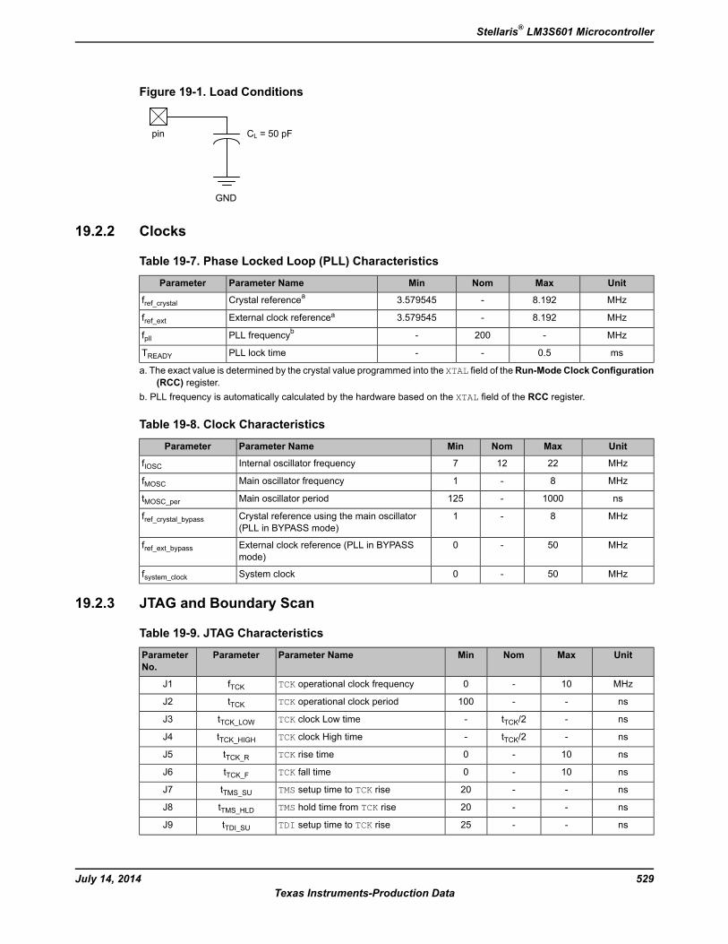
Figure 19-1. Load Conditions
CL = 50 pF
GND
pin
19.2.2 Clocks
Table 19-7. Phase Locked Loop (PLL) Characteristics
UnitMaxNomMinParameter NameParameter
MHz8.192-3.579545Crystal referenceafref_crystalMHz8.192-3.579545External clock referenceafref_extMHz-200-PLL frequencybfpllms0.5--PLL lock timeTREADY
a. The exact value is determined by the crystal value programmed into the XTAL field of theRun-Mode Clock Configuration(RCC) register.
b. PLL frequency is automatically calculated by the hardware based on the XTAL field of the RCC register.
Table 19-8. Clock Characteristics
UnitMaxNomMinParameter NameParameter
MHz22127Internal oscillator frequencyfIOSCMHz8-1Main oscillator frequencyfMOSCns1000-125Main oscillator periodtMOSC_perMHz8-1Crystal reference using the main oscillator
(PLL in BYPASS mode)fref_crystal_bypass
MHz50-0External clock reference (PLL in BYPASSmode)
fref_ext_bypass
MHz50-0System clockfsystem_clock
19.2.3 JTAG and Boundary Scan
Table 19-9. JTAG Characteristics
UnitMaxNomMinParameter NameParameterParameterNo.
MHz10-0TCK operational clock frequencyfTCKJ1
ns--100TCK operational clock periodtTCKJ2
ns-tTCK/2-TCK clock Low timetTCK_LOWJ3
ns-tTCK/2-TCK clock High timetTCK_HIGHJ4
ns10-0TCK rise timetTCK_RJ5
ns10-0TCK fall timetTCK_FJ6
ns--20TMS setup time to TCK risetTMS_SUJ7
ns--20TMS hold time from TCK risetTMS_HLDJ8
ns--25TDI setup time to TCK risetTDI_SUJ9
529July 14, 2014Texas Instruments-Production Data
Stellaris® LM3S601 Microcontroller
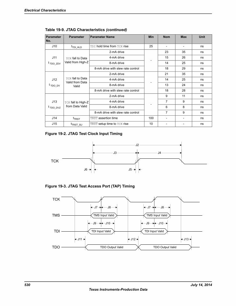
Table 19-9. JTAG Characteristics (continued)
UnitMaxNomMinParameter NameParameterParameterNo.
ns--25TDI hold time from TCK risetTDI_HLDJ10
ns3523
-
2-mA drive
TCK fall to DataValid from High-Z
J11t TDO_ZDV
ns26154-mA drive
ns25148-mA drive
ns29188-mA drive with slew rate control
ns3521
-
2-mA driveTCK fall to DataValid from Data
Valid
J12t TDO_DV
ns25144-mA drive
ns24138-mA drive
ns28188-mA drive with slew rate control
ns119
-
2-mA drive
TCK fall to High-Zfrom Data Valid
J13t TDO_DVZ
ns974-mA drive
ns868-mA drive
ns978-mA drive with slew rate control
ns--100TRST assertion timetTRSTJ14
ns--10TRST setup time to TCK risetTRST_SUJ15
Figure 19-2. JTAG Test Clock Input Timing
TCK
J6 J5
J3 J4
J2
Figure 19-3. JTAG Test Access Port (TAP) Timing
TDO Output Valid
TCK
TDO Output Valid
J12
TDO
TDI
TMS
TDI Input Valid TDI Input Valid
J13
J9 J10
TMS Input Valid
J9 J10
TMS Input Valid
J11
J7 J8J8J7
July 14, 2014530Texas Instruments-Production Data
Electrical Characteristics
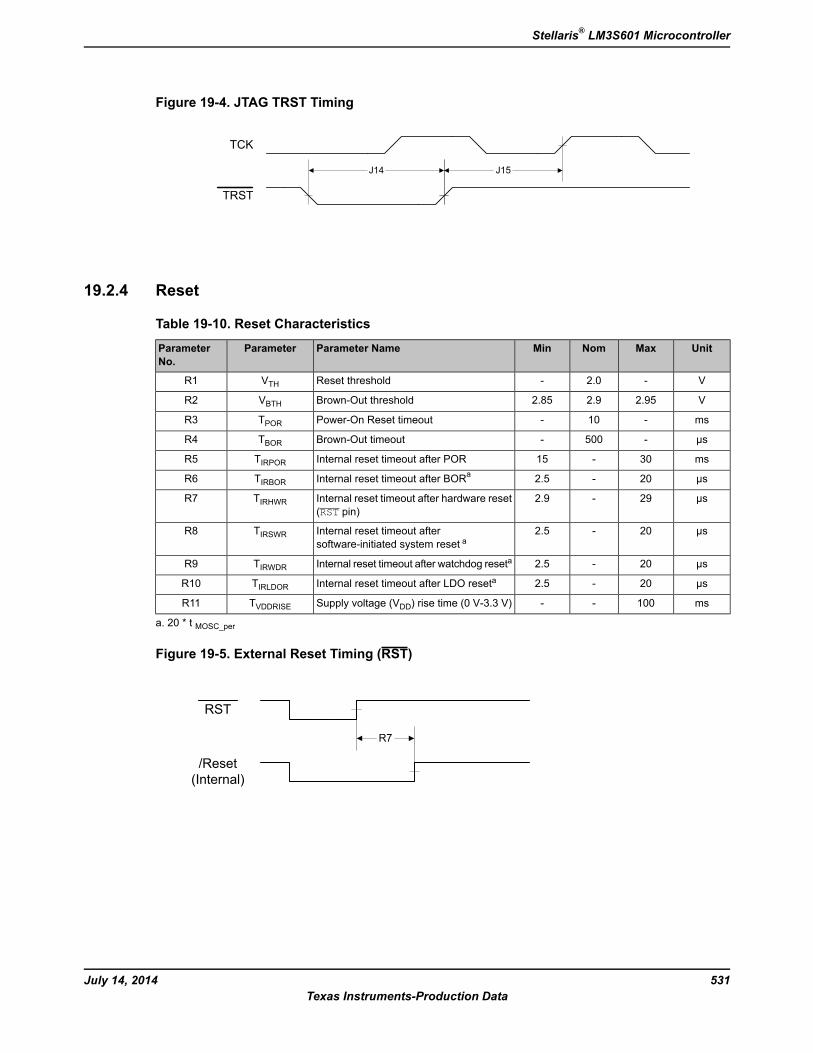
Figure 19-4. JTAG TRST Timing
TCK
J14 J15
TRST
19.2.4 Reset
Table 19-10. Reset Characteristics
UnitMaxNomMinParameter NameParameterParameterNo.
V-2.0-Reset thresholdVTHR1
V2.952.92.85Brown-Out thresholdVBTHR2
ms-10-Power-On Reset timeoutTPORR3
µs-500-Brown-Out timeoutTBORR4
ms30-15Internal reset timeout after PORTIRPORR5
µs20-2.5Internal reset timeout after BORaTIRBORR6
µs29-2.9Internal reset timeout after hardware reset(RST pin)
TIRHWRR7
µs20-2.5Internal reset timeout aftersoftware-initiated system reset a
TIRSWRR8
µs20-2.5Internal reset timeout after watchdog resetaTIRWDRR9
µs20-2.5Internal reset timeout after LDO resetaTIRLDORR10
ms100--Supply voltage (VDD) rise time (0 V-3.3 V)TVDDRISER11
a. 20 * t MOSC_per
Figure 19-5. External Reset Timing (RST)
RST
/Reset(Internal)
R7
531July 14, 2014Texas Instruments-Production Data
Stellaris® LM3S601 Microcontroller
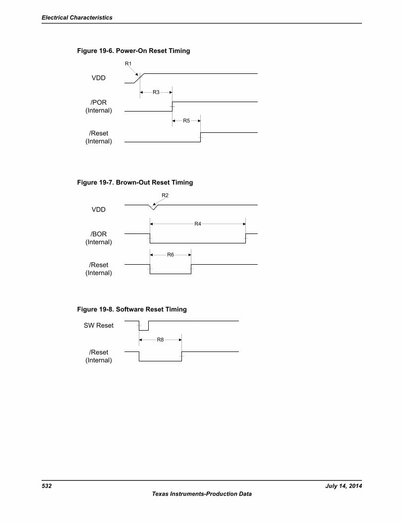
Figure 19-6. Power-On Reset Timing
VDD
/POR(Internal)
/Reset(Internal)
R3
R1
R5
Figure 19-7. Brown-Out Reset Timing
VDD
/BOR(Internal)
/Reset(Internal)
R2
R4
R6
Figure 19-8. Software Reset Timing
R8
SW Reset
/Reset(Internal)
July 14, 2014532Texas Instruments-Production Data
Electrical Characteristics
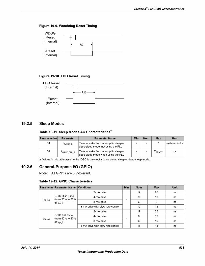
Figure 19-9. Watchdog Reset Timing
WDOGReset
(Internal)
/Reset(Internal)
R9
Figure 19-10. LDO Reset Timing
LDO Reset(Internal)
/Reset(Internal)
R10
19.2.5 Sleep Modes
Table 19-11. Sleep Modes AC Characteristicsa
UnitMaxNomMinParameter NameParameterParameter No
system clocks7--Time to wake from interrupt in sleep ordeep-sleep mode, not using the PLL
tWAKE_SD1
msTREADY--Time to wake from interrupt in sleep ordeep-sleep mode when using the PLL
tWAKE_PLL_SD2
a. Values in this table assume the IOSC is the clock source during sleep or deep-sleep mode.
19.2.6 General-Purpose I/O (GPIO)Note: All GPIOs are 5 V-tolerant.
Table 19-12. GPIO Characteristics
UnitMaxNomMinConditionParameter NameParameter
ns2617
-
2-mA driveGPIO Rise Time(from 20% to 80%of VDD)
tGPIORns1394-mA drive
ns968-mA drive
ns12108-mA drive with slew rate control
ns2517
-
2-mA driveGPIO Fall Time(from 80% to 20%of VDD)
tGPIOFns1284-mA drive
ns1068-mA drive
ns13118-mA drive with slew rate control
533July 14, 2014Texas Instruments-Production Data
Stellaris® LM3S601 Microcontroller
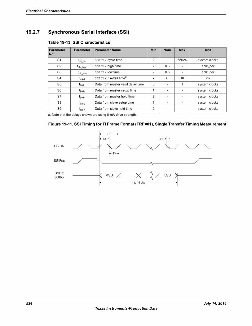
19.2.7 Synchronous Serial Interface (SSI)
Table 19-13. SSI Characteristics
UnitMaxNomMinParameter NameParameterParameterNo.
system clocks65024-2SSIClk cycle timetclk_perS1
t clk_per-0.5-SSIClk high timetclk_highS2
t clk_per-0.5-SSIClk low timetclk_lowS3
ns106-SSIClk rise/fall timeatclkrfS4
system clocks1-0Data from master valid delay timetDMdS5
system clocks--1Data from master setup timetDMsS6
system clocks--2Data from master hold timetDMhS7
system clocks--1Data from slave setup timetDSsS8
system clocks--2Data from slave hold timetDShS9
a. Note that the delays shown are using 8-mA drive strength.
Figure 19-11. SSI Timing for TI Frame Format (FRF=01), Single Transfer Timing Measurement
SSIClk
SSIFss
SSITxSSIRx MSB LSB
S2
S3
S1
S4
4 to 16 bits
July 14, 2014534Texas Instruments-Production Data
Electrical Characteristics
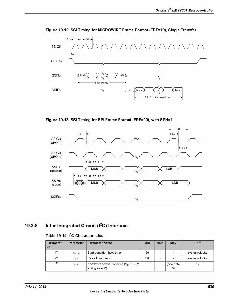
Figure 19-12. SSI Timing for MICROWIRE Frame Format (FRF=10), Single Transfer
0
SSIClk
SSIFss
SSITx
SSIRx
MSB LSB
MSB LSB
S2
S3
S1
8-bit control
4 to 16 bits output data
Figure 19-13. SSI Timing for SPI Frame Format (FRF=00), with SPH=1
SSIClk(SPO=1)
SSITx(master)
SSIRx(slave) LSB
SSIClk(SPO=0)
S2
S1
S4
SSIFss
LSB
S3
MSB
S5
S6 S7
S9S8
MSB
19.2.8 Inter-Integrated Circuit (I2C) Interface
Table 19-14. I2C Characteristics
UnitMaxNomMinParameter NameParameterParameterNo.
system clocks--36Start condition hold timetSCHI1a
system clocks--36Clock Low periodtLPI2a
ns(see noteb)
--I2CSCL/I2CSDA rise time (VIL =0.5 Vto V IH =2.4 V)
tSRTI3b
535July 14, 2014Texas Instruments-Production Data
Stellaris® LM3S601 Microcontroller
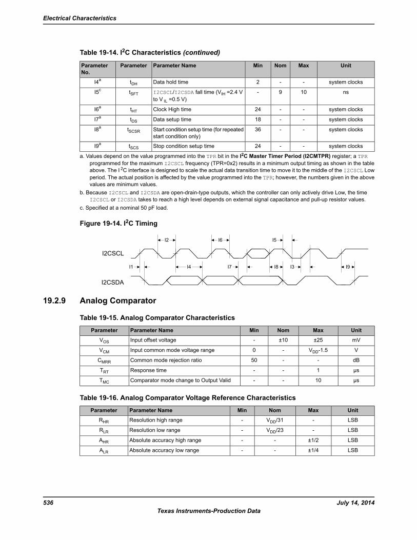
Table 19-14. I2C Characteristics (continued)
UnitMaxNomMinParameter NameParameterParameterNo.
system clocks--2Data hold timetDHI4a
ns109-I2CSCL/I2CSDA fall time (VIH =2.4 Vto V IL =0.5 V)
tSFTI5c
system clocks--24Clock High timetHTI6a
system clocks--18Data setup timetDSI7a
system clocks--36Start condition setup time (for repeatedstart condition only)
tSCSRI8a
system clocks--24Stop condition setup timetSCSI9a
a. Values depend on the value programmed into the TPR bit in the I2C Master Timer Period (I2CMTPR) register; a TPRprogrammed for the maximum I2CSCL frequency (TPR=0x2) results in a minimum output timing as shown in the tableabove. The I 2C interface is designed to scale the actual data transition time to move it to the middle of the I2CSCL Lowperiod. The actual position is affected by the value programmed into the TPR; however, the numbers given in the abovevalues are minimum values.
b. Because I2CSCL and I2CSDA are open-drain-type outputs, which the controller can only actively drive Low, the timeI2CSCL or I2CSDA takes to reach a high level depends on external signal capacitance and pull-up resistor values.
c. Specified at a nominal 50 pF load.
Figure 19-14. I2C Timing
I2CSCL
I2CSDA
I1
I2
I4
I6
I7 I8
I5
I3 I9
19.2.9 Analog Comparator
Table 19-15. Analog Comparator Characteristics
UnitMaxNomMinParameter NameParameter
mV±25±10-Input offset voltageVOSVVDD-1.5-0Input common mode voltage rangeVCMdB--50Common mode rejection ratioCMRR
µs1--Response timeTRTµs10--Comparator mode change to Output ValidTMC
Table 19-16. Analog Comparator Voltage Reference Characteristics
UnitMaxNomMinParameter NameParameter
LSB-VDD/31-Resolution high rangeRHR
LSB-VDD/23-Resolution low rangeRLR
LSB±1/2--Absolute accuracy high rangeAHRLSB±1/4--Absolute accuracy low rangeALR
July 14, 2014536Texas Instruments-Production Data
Electrical Characteristics
A Serial Flash LoaderA.1 Serial Flash Loader
The Stellaris® serial flash loader is a preprogrammed flash-resident utility used to download codeto the flash memory of a device without the use of a debug interface. The serial flash loader usesa simple packet interface to provide synchronous communication with the device. The flash loaderruns off the crystal and does not enable the PLL, so its speed is determined by the crystal used.The two serial interfaces that can be used are the UART0 and SSI0 interfaces. For simplicity, boththe data format and communication protocol are identical for both serial interfaces.
A.2 InterfacesOnce communication with the flash loader is established via one of the serial interfaces, that interfaceis used until the flash loader is reset or new code takes over. For example, once you startcommunicating using the SSI port, communications with the flash loader via the UART are disableduntil the device is reset.
A.2.1 UARTThe Universal Asynchronous Receivers/Transmitters (UART) communication uses a fixed serialformat of 8 bits of data, no parity, and 1 stop bit. The baud rate used for communication isautomatically detected by the flash loader and can be any valid baud rate supported by the hostand the device. The auto detection sequence requires that the baud rate should be no more than1/32 the crystal frequency of the board that is running the serial flash loader. This is actually thesame as the hardware limitation for the maximum baud rate for any UART on a Stellaris devicewhich is calculated as follows:
Max Baud Rate = System Clock Frequency / 16
In order to determine the baud rate, the serial flash loader needs to determine the relationshipbetween its own crystal frequency and the baud rate. This is enough information for the flash loaderto configure its UART to the same baud rate as the host. This automatic baud-rate detection allowsthe host to use any valid baud rate that it wants to communicate with the device.
The method used to perform this automatic synchronization relies on the host sending the flashloader two bytes that are both 0x55. This generates a series of pulses to the flash loader that it canuse to calculate the ratios needed to program the UART to match the host’s baud rate. After thehost sends the pattern, it attempts to read back one byte of data from the UART. The flash loaderreturns the value of 0xCC to indicate successful detection of the baud rate. If this byte is not receivedafter at least twice the time required to transfer the two bytes, the host can resend another patternof 0x55, 0x55, and wait for the 0xCC byte again until the flash loader acknowledges that it hasreceived a synchronization pattern correctly. For example, the time to wait for data back from theflash loader should be calculated as at least 2*(20(bits/sync)/baud rate (bits/sec)). For a baud rateof 115200, this time is 2*(20/115200) or 0.35 ms.
A.2.2 SSIThe Synchronous Serial Interface (SSI) port also uses a fixed serial format for communications,with the framing defined as Motorola format with SPH set to 1 and SPO set to 1. See “FrameFormats” on page 374 in the SSI chapter for more information on formats for this transfer protocol.Like the UART, this interface has hardware requirements that limit the maximum speed that the SSIclock can run. This allows the SSI clock to be at most 1/12 the crystal frequency of the board running
537July 14, 2014Texas Instruments-Production Data
Stellaris® LM3S601 Microcontroller
the flash loader. Since the host device is the master, the SSI on the flash loader device does notneed to determine the clock as it is provided directly by the host.
A.3 Packet HandlingAll communications, with the exception of the UART auto-baud, are done via defined packets thatare acknowledged (ACK) or not acknowledged (NAK) by the devices. The packets use the sameformat for receiving and sending packets, including the method used to acknowledge successful orunsuccessful reception of a packet.
A.3.1 Packet FormatAll packets sent and received from the device use the following byte-packed format.
struct unsigned char ucSize; unsigned char ucCheckSum; unsigned char Data[];;
ucSize The first byte received holds the total size of the transfer includingthe size and checksum bytes.
ucChecksum This holds a simple checksum of the bytes in the data buffer only.The algorithm is Data[0]+Data[1]+…+ Data[ucSize-3].
Data This is the raw data intended for the device, which is formatted insome form of command interface. There should be ucSize–2bytes of data provided in this buffer to or from the device.
A.3.2 Sending PacketsThe actual bytes of the packet can be sent individually or all at once; the only limitation is thatcommands that cause flash memory access should limit the download sizes to prevent losing bytesduring flash programming. This limitation is discussed further in the section that describes the serialflash loader command, COMMAND_SEND_DATA (see “COMMAND_SEND_DATA(0x24)” on page 540).
Once the packet has been formatted correctly by the host, it should be sent out over the UART orSSI interface. Then the host should poll the UART or SSI interface for the first non-zero data returnedfrom the device. The first non-zero byte will either be an ACK (0xCC) or a NAK (0x33) byte fromthe device indicating the packet was received successfully (ACK) or unsuccessfully (NAK). Thisdoes not indicate that the actual contents of the command issued in the data portion of the packetwere valid, just that the packet was received correctly.
A.3.3 Receiving PacketsThe flash loader sends a packet of data in the same format that it receives a packet. The flash loadermay transfer leading zero data before the first actual byte of data is sent out. The first non-zero byteis the size of the packet followed by a checksum byte, and finally followed by the data itself. Thereis no break in the data after the first non-zero byte is sent from the flash loader. Once the devicecommunicating with the flash loader receives all the bytes, it must either ACK or NAK the packet toindicate that the transmission was successful. The appropriate response after sending a NAK tothe flash loader is to resend the command that failed and request the data again. If needed, thehost may send leading zeros before sending down the ACK/NAK signal to the flash loader, as the
July 14, 2014538Texas Instruments-Production Data
Serial Flash Loader
flash loader only accepts the first non-zero data as a valid response. This zero padding is neededby the SSI interface in order to receive data to or from the flash loader.
A.4 CommandsThe next section defines the list of commands that can be sent to the flash loader. The first byte ofthe data should always be one of the defined commands, followed by data or parameters asdetermined by the command that is sent.
A.4.1 COMMAND_PING (0X20)This command simply accepts the command and sets the global status to success. The format ofthe packet is as follows:
Byte[0] = 0x03;Byte[1] = checksum(Byte[2]);Byte[2] = COMMAND_PING;
The ping command has 3 bytes and the value for COMMAND_PING is 0x20 and the checksum of onebyte is that same byte, making Byte[1] also 0x20. Since the ping command has no real return status,the receipt of an ACK can be interpreted as a successful ping to the flash loader.
A.4.2 COMMAND_GET_STATUS (0x23)This command returns the status of the last command that was issued. Typically, this commandshould be sent after every command to ensure that the previous command was successful or toproperly respond to a failure. The command requires one byte in the data of the packet and shouldbe followed by reading a packet with one byte of data that contains a status code. The last step isto ACK or NAK the received data so the flash loader knows that the data has been read.
Byte[0] = 0x03Byte[1] = checksum(Byte[2])Byte[2] = COMMAND_GET_STATUS
A.4.3 COMMAND_DOWNLOAD (0x21)This command is sent to the flash loader to indicate where to store data and how many bytes willbe sent by the COMMAND_SEND_DATA commands that follow. The command consists of two 32-bitvalues that are both transferred MSB first. The first 32-bit value is the address to start programmingdata into, while the second is the 32-bit size of the data that will be sent. This command also triggersan erase of the full area to be programmed so this command takes longer than other commands.This results in a longer time to receive the ACK/NAK back from the board. This command shouldbe followed by a COMMAND_GET_STATUS to ensure that the Program Address and Program sizeare valid for the device running the flash loader.
The format of the packet to send this command is a follows:
Byte[0] = 11Byte[1] = checksum(Bytes[2:10])Byte[2] = COMMAND_DOWNLOADByte[3] = Program Address [31:24]Byte[4] = Program Address [23:16]Byte[5] = Program Address [15:8]Byte[6] = Program Address [7:0]Byte[7] = Program Size [31:24]
539July 14, 2014Texas Instruments-Production Data
Stellaris® LM3S601 Microcontroller
Byte[8] = Program Size [23:16]Byte[9] = Program Size [15:8]Byte[10] = Program Size [7:0]
A.4.4 COMMAND_SEND_DATA (0x24)This command should only follow a COMMAND_DOWNLOAD command or anotherCOMMAND_SEND_DATA command if more data is needed. Consecutive send data commandsautomatically increment address and continue programming from the previous location. The callershould limit transfers of data to a maximum 8 bytes of packet data to allow the flash to programsuccessfully and not overflow input buffers of the serial interfaces. The command terminatesprogramming once the number of bytes indicated by the COMMAND_DOWNLOAD command has beenreceived. Each time this function is called it should be followed by a COMMAND_GET_STATUS toensure that the data was successfully programmed into the flash. If the flash loader sends a NAKto this command, the flash loader does not increment the current address to allow retransmissionof the previous data.
Byte[0] = 11Byte[1] = checksum(Bytes[2:10])Byte[2] = COMMAND_SEND_DATAByte[3] = Data[0]Byte[4] = Data[1]Byte[5] = Data[2]Byte[6] = Data[3]Byte[7] = Data[4]Byte[8] = Data[5]Byte[9] = Data[6]Byte[10] = Data[7]
A.4.5 COMMAND_RUN (0x22)This command is used to tell the flash loader to execute from the address passed as the parameterin this command. This command consists of a single 32-bit value that is interpreted as the addressto execute. The 32-bit value is transmitted MSB first and the flash loader responds with an ACKsignal back to the host device before actually executing the code at the given address. This allowsthe host to know that the command was received successfully and the code is now running.
Byte[0] = 7Byte[1] = checksum(Bytes[2:6])Byte[2] = COMMAND_RUNByte[3] = Execute Address[31:24]Byte[4] = Execute Address[23:16]Byte[5] = Execute Address[15:8]Byte[6] = Execute Address[7:0]
A.4.6 COMMAND_RESET (0x25)This command is used to tell the flash loader device to reset. This is useful when downloading anew image that overwrote the flash loader and wants to start from a full reset. Unlike theCOMMAND_RUN command, this allows the initial stack pointer to be read by the hardware and setup for the new code. It can also be used to reset the flash loader if a critical error occurs and thehost device wants to restart communication with the flash loader.
July 14, 2014540Texas Instruments-Production Data
Serial Flash Loader
Byte[0] = 3Byte[1] = checksum(Byte[2])Byte[2] = COMMAND_RESET
The flash loader responds with an ACK signal back to the host device before actually executing thesoftware reset to the device running the flash loader. This allows the host to know that the commandwas received successfully and the part will be reset.
541July 14, 2014Texas Instruments-Production Data
Stellaris® LM3S601 Microcontroller
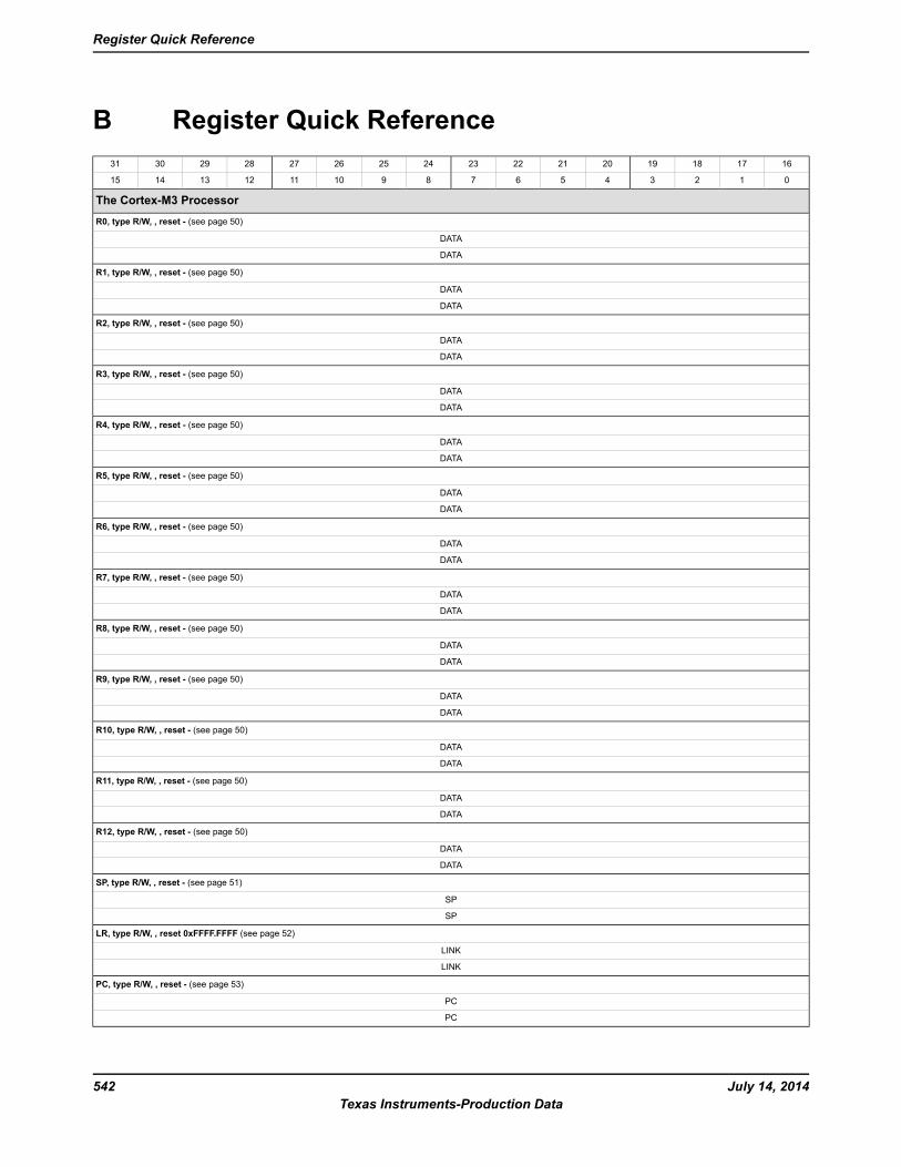
B Register Quick Reference16171819202122232425262728293031
0123456789101112131415
The Cortex-M3 ProcessorR0, type R/W, , reset - (see page 50)
DATA
DATA
R1, type R/W, , reset - (see page 50)
DATA
DATA
R2, type R/W, , reset - (see page 50)
DATA
DATA
R3, type R/W, , reset - (see page 50)
DATA
DATA
R4, type R/W, , reset - (see page 50)
DATA
DATA
R5, type R/W, , reset - (see page 50)
DATA
DATA
R6, type R/W, , reset - (see page 50)
DATA
DATA
R7, type R/W, , reset - (see page 50)
DATA
DATA
R8, type R/W, , reset - (see page 50)
DATA
DATA
R9, type R/W, , reset - (see page 50)
DATA
DATA
R10, type R/W, , reset - (see page 50)
DATA
DATA
R11, type R/W, , reset - (see page 50)
DATA
DATA
R12, type R/W, , reset - (see page 50)
DATA
DATA
SP, type R/W, , reset - (see page 51)
SP
SP
LR, type R/W, , reset 0xFFFF.FFFF (see page 52)
LINK
LINK
PC, type R/W, , reset - (see page 53)
PC
PC
July 14, 2014542Texas Instruments-Production Data
Register Quick Reference
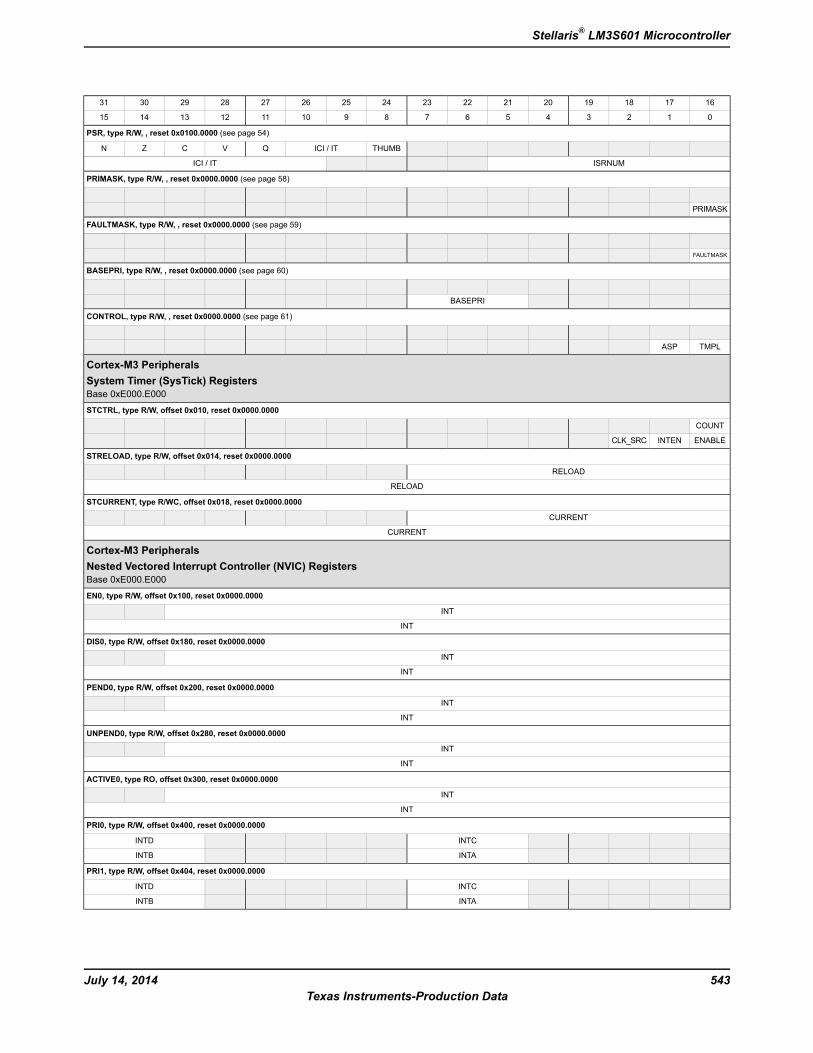
16171819202122232425262728293031
0123456789101112131415
PSR, type R/W, , reset 0x0100.0000 (see page 54)
THUMBICI / ITQVCZN
ISRNUMICI / IT
PRIMASK, type R/W, , reset 0x0000.0000 (see page 58)
PRIMASK
FAULTMASK, type R/W, , reset 0x0000.0000 (see page 59)
FAULTMASK
BASEPRI, type R/W, , reset 0x0000.0000 (see page 60)
BASEPRI
CONTROL, type R/W, , reset 0x0000.0000 (see page 61)
TMPLASP
Cortex-M3 PeripheralsSystem Timer (SysTick) RegistersBase 0xE000.E000
STCTRL, type R/W, offset 0x010, reset 0x0000.0000
COUNT
ENABLEINTENCLK_SRC
STRELOAD, type R/W, offset 0x014, reset 0x0000.0000
RELOAD
RELOAD
STCURRENT, type R/WC, offset 0x018, reset 0x0000.0000
CURRENT
CURRENT
Cortex-M3 PeripheralsNested Vectored Interrupt Controller (NVIC) RegistersBase 0xE000.E000
EN0, type R/W, offset 0x100, reset 0x0000.0000
INT
INT
DIS0, type R/W, offset 0x180, reset 0x0000.0000
INT
INT
PEND0, type R/W, offset 0x200, reset 0x0000.0000
INT
INT
UNPEND0, type R/W, offset 0x280, reset 0x0000.0000
INT
INT
ACTIVE0, type RO, offset 0x300, reset 0x0000.0000
INT
INT
PRI0, type R/W, offset 0x400, reset 0x0000.0000
INTCINTD
INTAINTB
PRI1, type R/W, offset 0x404, reset 0x0000.0000
INTCINTD
INTAINTB
543July 14, 2014Texas Instruments-Production Data
Stellaris® LM3S601 Microcontroller
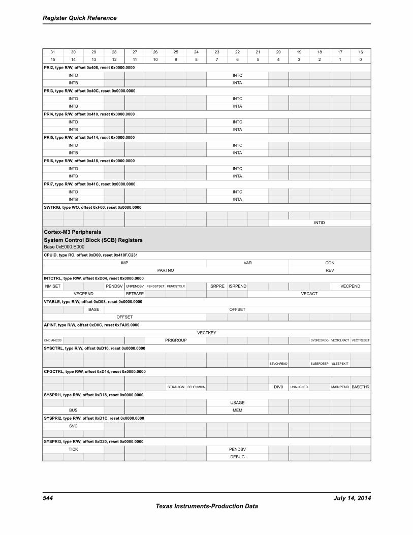
16171819202122232425262728293031
0123456789101112131415
PRI2, type R/W, offset 0x408, reset 0x0000.0000
INTCINTD
INTAINTB
PRI3, type R/W, offset 0x40C, reset 0x0000.0000
INTCINTD
INTAINTB
PRI4, type R/W, offset 0x410, reset 0x0000.0000
INTCINTD
INTAINTB
PRI5, type R/W, offset 0x414, reset 0x0000.0000
INTCINTD
INTAINTB
PRI6, type R/W, offset 0x418, reset 0x0000.0000
INTCINTD
INTAINTB
PRI7, type R/W, offset 0x41C, reset 0x0000.0000
INTCINTD
INTAINTB
SWTRIG, type WO, offset 0xF00, reset 0x0000.0000
INTID
Cortex-M3 PeripheralsSystem Control Block (SCB) RegistersBase 0xE000.E000
CPUID, type RO, offset 0xD00, reset 0x410F.C231
CONVARIMP
REVPARTNO
INTCTRL, type R/W, offset 0xD04, reset 0x0000.0000
VECPENDISRPENDISRPREPENDSTCLRPENDSTSETUNPENDSVPENDSVNMISET
VECACTRETBASEVECPEND
VTABLE, type R/W, offset 0xD08, reset 0x0000.0000
OFFSETBASE
OFFSET
APINT, type R/W, offset 0xD0C, reset 0xFA05.0000
VECTKEY
VECTRESETVECTCLRACTSYSRESREQPRIGROUPENDIANESS
SYSCTRL, type R/W, offset 0xD10, reset 0x0000.0000
SLEEPEXITSLEEPDEEPSEVONPEND
CFGCTRL, type R/W, offset 0xD14, reset 0x0000.0000
BASETHRMAINPENDUNALIGNEDDIV0BFHFNMIGNSTKALIGN
SYSPRI1, type R/W, offset 0xD18, reset 0x0000.0000
USAGE
MEMBUS
SYSPRI2, type R/W, offset 0xD1C, reset 0x0000.0000
SVC
SYSPRI3, type R/W, offset 0xD20, reset 0x0000.0000
PENDSVTICK
DEBUG
July 14, 2014544Texas Instruments-Production Data
Register Quick Reference
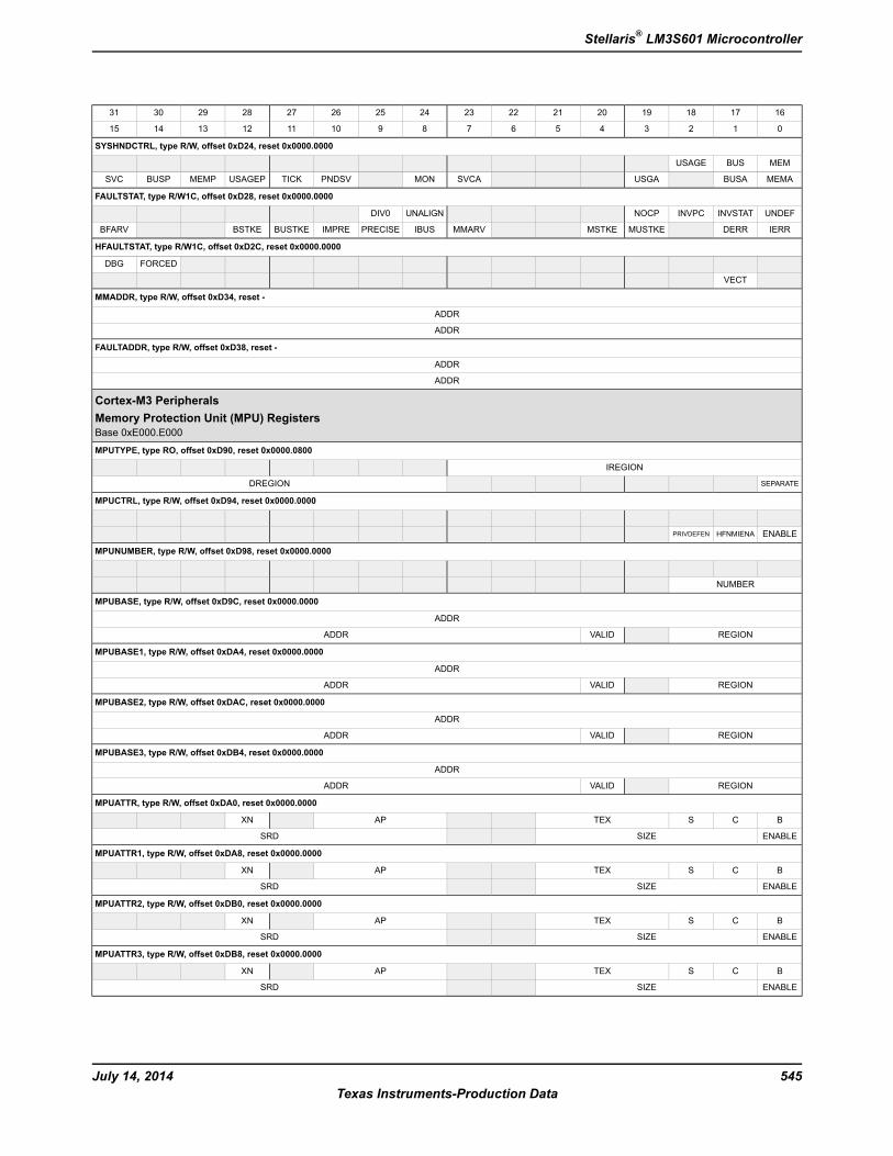
16171819202122232425262728293031
0123456789101112131415
SYSHNDCTRL, type R/W, offset 0xD24, reset 0x0000.0000
MEMBUSUSAGE
MEMABUSAUSGASVCAMONPNDSVTICKUSAGEPMEMPBUSPSVC
FAULTSTAT, type R/W1C, offset 0xD28, reset 0x0000.0000
UNDEFINVSTATINVPCNOCPUNALIGNDIV0
IERRDERRMUSTKEMSTKEMMARVIBUSPRECISEIMPREBUSTKEBSTKEBFARV
HFAULTSTAT, type R/W1C, offset 0xD2C, reset 0x0000.0000
FORCEDDBG
VECT
MMADDR, type R/W, offset 0xD34, reset -
ADDR
ADDR
FAULTADDR, type R/W, offset 0xD38, reset -
ADDR
ADDR
Cortex-M3 PeripheralsMemory Protection Unit (MPU) RegistersBase 0xE000.E000
MPUTYPE, type RO, offset 0xD90, reset 0x0000.0800
IREGION
SEPARATEDREGION
MPUCTRL, type R/W, offset 0xD94, reset 0x0000.0000
ENABLEHFNMIENAPRIVDEFEN
MPUNUMBER, type R/W, offset 0xD98, reset 0x0000.0000
NUMBER
MPUBASE, type R/W, offset 0xD9C, reset 0x0000.0000
ADDR
REGIONVALIDADDR
MPUBASE1, type R/W, offset 0xDA4, reset 0x0000.0000
ADDR
REGIONVALIDADDR
MPUBASE2, type R/W, offset 0xDAC, reset 0x0000.0000
ADDR
REGIONVALIDADDR
MPUBASE3, type R/W, offset 0xDB4, reset 0x0000.0000
ADDR
REGIONVALIDADDR
MPUATTR, type R/W, offset 0xDA0, reset 0x0000.0000
BCSTEXAPXN
ENABLESIZESRD
MPUATTR1, type R/W, offset 0xDA8, reset 0x0000.0000
BCSTEXAPXN
ENABLESIZESRD
MPUATTR2, type R/W, offset 0xDB0, reset 0x0000.0000
BCSTEXAPXN
ENABLESIZESRD
MPUATTR3, type R/W, offset 0xDB8, reset 0x0000.0000
BCSTEXAPXN
ENABLESIZESRD
545July 14, 2014Texas Instruments-Production Data
Stellaris® LM3S601 Microcontroller
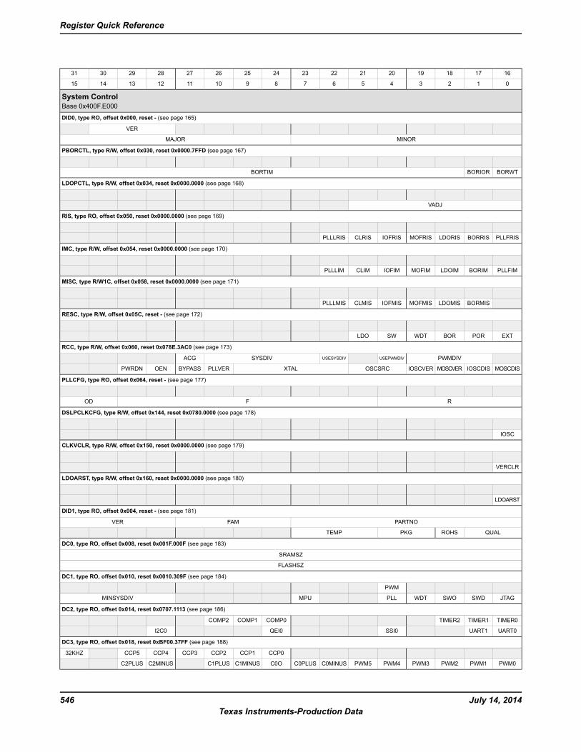
16171819202122232425262728293031
0123456789101112131415
System ControlBase 0x400F.E000
DID0, type RO, offset 0x000, reset - (see page 165)
VER
MINORMAJOR
PBORCTL, type R/W, offset 0x030, reset 0x0000.7FFD (see page 167)
BORWTBORIORBORTIM
LDOPCTL, type R/W, offset 0x034, reset 0x0000.0000 (see page 168)
VADJ
RIS, type RO, offset 0x050, reset 0x0000.0000 (see page 169)
PLLFRISBORRISLDORISMOFRISIOFRISCLRISPLLLRIS
IMC, type R/W, offset 0x054, reset 0x0000.0000 (see page 170)
PLLFIMBORIMLDOIMMOFIMIOFIMCLIMPLLLIM
MISC, type R/W1C, offset 0x058, reset 0x0000.0000 (see page 171)
BORMISLDOMISMOFMISIOFMISCLMISPLLLMIS
RESC, type R/W, offset 0x05C, reset - (see page 172)
EXTPORBORWDTSWLDO
RCC, type R/W, offset 0x060, reset 0x078E.3AC0 (see page 173)
PWMDIVUSEPWMDIVUSESYSDIVSYSDIVACG
MOSCDISIOSCDISMOSCVERIOSCVEROSCSRCXTALPLLVERBYPASSOENPWRDN
PLLCFG, type RO, offset 0x064, reset - (see page 177)
RFOD
DSLPCLKCFG, type R/W, offset 0x144, reset 0x0780.0000 (see page 178)
IOSC
CLKVCLR, type R/W, offset 0x150, reset 0x0000.0000 (see page 179)
VERCLR
LDOARST, type R/W, offset 0x160, reset 0x0000.0000 (see page 180)
LDOARST
DID1, type RO, offset 0x004, reset - (see page 181)
PARTNOFAMVER
QUALROHSPKGTEMP
DC0, type RO, offset 0x008, reset 0x001F.000F (see page 183)
SRAMSZ
FLASHSZ
DC1, type RO, offset 0x010, reset 0x0010.309F (see page 184)
PWM
JTAGSWDSWOWDTPLLMPUMINSYSDIV
DC2, type RO, offset 0x014, reset 0x0707.1113 (see page 186)
TIMER0TIMER1TIMER2COMP0COMP1COMP2
UART0UART1SSI0QEI0I2C0
DC3, type RO, offset 0x018, reset 0xBF00.37FF (see page 188)
CCP0CCP1CCP2CCP3CCP4CCP532KHZ
PWM0PWM1PWM2PWM3PWM4PWM5C0MINUSC0PLUSC0OC1MINUSC1PLUSC2MINUSC2PLUS
July 14, 2014546Texas Instruments-Production Data
Register Quick Reference
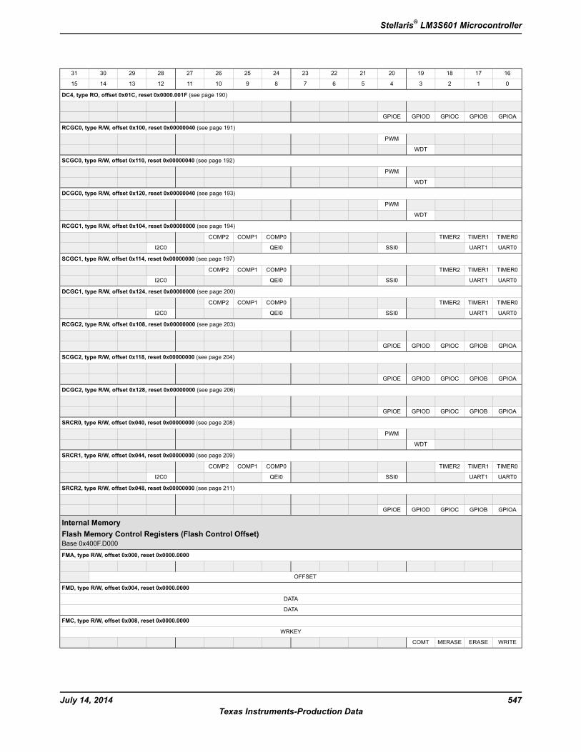
16171819202122232425262728293031
0123456789101112131415
DC4, type RO, offset 0x01C, reset 0x0000.001F (see page 190)
GPIOAGPIOBGPIOCGPIODGPIOE
RCGC0, type R/W, offset 0x100, reset 0x00000040 (see page 191)
PWM
WDT
SCGC0, type R/W, offset 0x110, reset 0x00000040 (see page 192)
PWM
WDT
DCGC0, type R/W, offset 0x120, reset 0x00000040 (see page 193)
PWM
WDT
RCGC1, type R/W, offset 0x104, reset 0x00000000 (see page 194)
TIMER0TIMER1TIMER2COMP0COMP1COMP2
UART0UART1SSI0QEI0I2C0
SCGC1, type R/W, offset 0x114, reset 0x00000000 (see page 197)
TIMER0TIMER1TIMER2COMP0COMP1COMP2
UART0UART1SSI0QEI0I2C0
DCGC1, type R/W, offset 0x124, reset 0x00000000 (see page 200)
TIMER0TIMER1TIMER2COMP0COMP1COMP2
UART0UART1SSI0QEI0I2C0
RCGC2, type R/W, offset 0x108, reset 0x00000000 (see page 203)
GPIOAGPIOBGPIOCGPIODGPIOE
SCGC2, type R/W, offset 0x118, reset 0x00000000 (see page 204)
GPIOAGPIOBGPIOCGPIODGPIOE
DCGC2, type R/W, offset 0x128, reset 0x00000000 (see page 206)
GPIOAGPIOBGPIOCGPIODGPIOE
SRCR0, type R/W, offset 0x040, reset 0x00000000 (see page 208)
PWM
WDT
SRCR1, type R/W, offset 0x044, reset 0x00000000 (see page 209)
TIMER0TIMER1TIMER2COMP0COMP1COMP2
UART0UART1SSI0QEI0I2C0
SRCR2, type R/W, offset 0x048, reset 0x00000000 (see page 211)
GPIOAGPIOBGPIOCGPIODGPIOE
Internal MemoryFlash Memory Control Registers (Flash Control Offset)Base 0x400F.D000
FMA, type R/W, offset 0x000, reset 0x0000.0000
OFFSET
FMD, type R/W, offset 0x004, reset 0x0000.0000
DATA
DATA
FMC, type R/W, offset 0x008, reset 0x0000.0000
WRKEY
WRITEERASEMERASECOMT
547July 14, 2014Texas Instruments-Production Data
Stellaris® LM3S601 Microcontroller
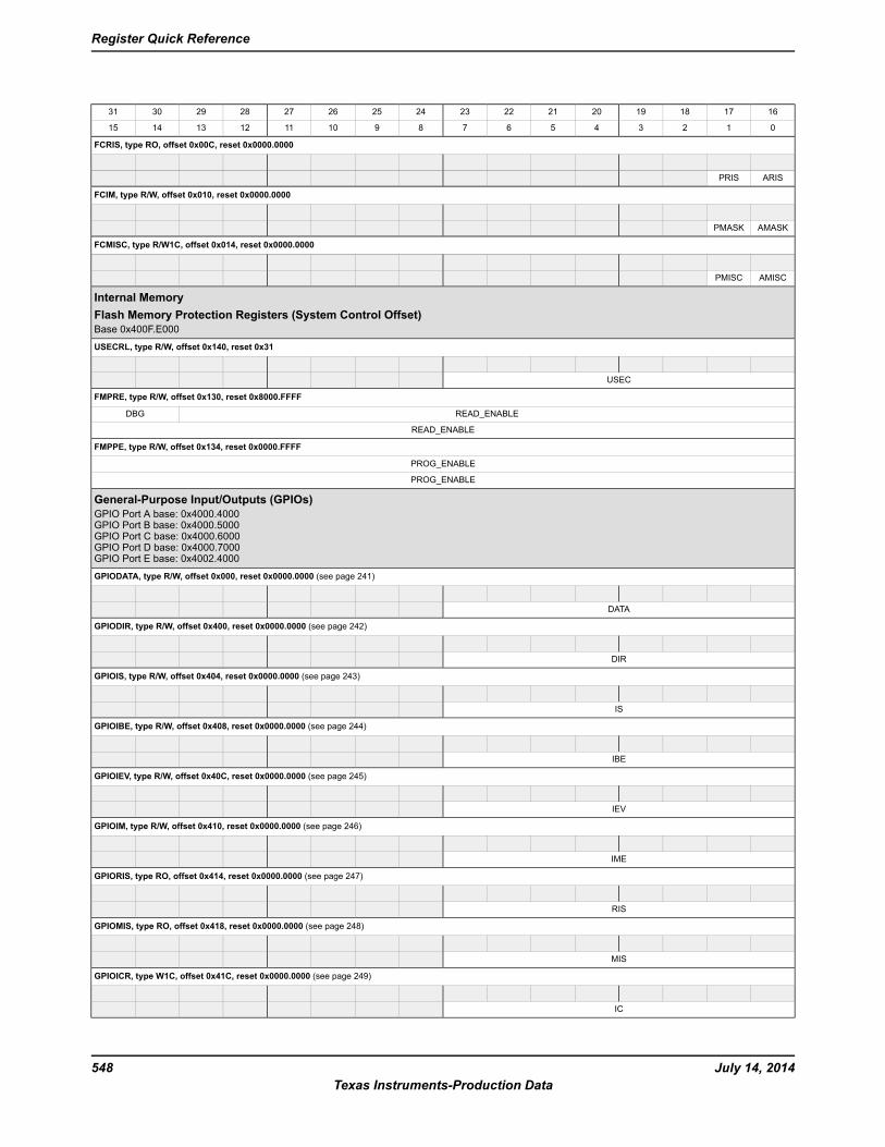
16171819202122232425262728293031
0123456789101112131415
FCRIS, type RO, offset 0x00C, reset 0x0000.0000
ARISPRIS
FCIM, type R/W, offset 0x010, reset 0x0000.0000
AMASKPMASK
FCMISC, type R/W1C, offset 0x014, reset 0x0000.0000
AMISCPMISC
Internal MemoryFlash Memory Protection Registers (System Control Offset)Base 0x400F.E000
USECRL, type R/W, offset 0x140, reset 0x31
USEC
FMPRE, type R/W, offset 0x130, reset 0x8000.FFFF
READ_ENABLEDBG
READ_ENABLE
FMPPE, type R/W, offset 0x134, reset 0x0000.FFFF
PROG_ENABLE
PROG_ENABLE
General-Purpose Input/Outputs (GPIOs)GPIO Port A base: 0x4000.4000GPIO Port B base: 0x4000.5000GPIO Port C base: 0x4000.6000GPIO Port D base: 0x4000.7000GPIO Port E base: 0x4002.4000
GPIODATA, type R/W, offset 0x000, reset 0x0000.0000 (see page 241)
DATA
GPIODIR, type R/W, offset 0x400, reset 0x0000.0000 (see page 242)
DIR
GPIOIS, type R/W, offset 0x404, reset 0x0000.0000 (see page 243)
IS
GPIOIBE, type R/W, offset 0x408, reset 0x0000.0000 (see page 244)
IBE
GPIOIEV, type R/W, offset 0x40C, reset 0x0000.0000 (see page 245)
IEV
GPIOIM, type R/W, offset 0x410, reset 0x0000.0000 (see page 246)
IME
GPIORIS, type RO, offset 0x414, reset 0x0000.0000 (see page 247)
RIS
GPIOMIS, type RO, offset 0x418, reset 0x0000.0000 (see page 248)
MIS
GPIOICR, type W1C, offset 0x41C, reset 0x0000.0000 (see page 249)
IC
July 14, 2014548Texas Instruments-Production Data
Register Quick Reference
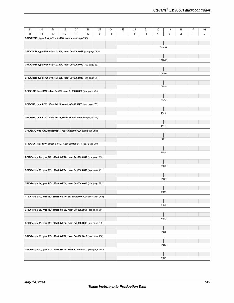
16171819202122232425262728293031
0123456789101112131415
GPIOAFSEL, type R/W, offset 0x420, reset - (see page 250)
AFSEL
GPIODR2R, type R/W, offset 0x500, reset 0x0000.00FF (see page 252)
DRV2
GPIODR4R, type R/W, offset 0x504, reset 0x0000.0000 (see page 253)
DRV4
GPIODR8R, type R/W, offset 0x508, reset 0x0000.0000 (see page 254)
DRV8
GPIOODR, type R/W, offset 0x50C, reset 0x0000.0000 (see page 255)
ODE
GPIOPUR, type R/W, offset 0x510, reset 0x0000.00FF (see page 256)
PUE
GPIOPDR, type R/W, offset 0x514, reset 0x0000.0000 (see page 257)
PDE
GPIOSLR, type R/W, offset 0x518, reset 0x0000.0000 (see page 258)
SRL
GPIODEN, type R/W, offset 0x51C, reset 0x0000.00FF (see page 259)
DEN
GPIOPeriphID4, type RO, offset 0xFD0, reset 0x0000.0000 (see page 260)
PID4
GPIOPeriphID5, type RO, offset 0xFD4, reset 0x0000.0000 (see page 261)
PID5
GPIOPeriphID6, type RO, offset 0xFD8, reset 0x0000.0000 (see page 262)
PID6
GPIOPeriphID7, type RO, offset 0xFDC, reset 0x0000.0000 (see page 263)
PID7
GPIOPeriphID0, type RO, offset 0xFE0, reset 0x0000.0061 (see page 264)
PID0
GPIOPeriphID1, type RO, offset 0xFE4, reset 0x0000.0000 (see page 265)
PID1
GPIOPeriphID2, type RO, offset 0xFE8, reset 0x0000.0018 (see page 266)
PID2
GPIOPeriphID3, type RO, offset 0xFEC, reset 0x0000.0001 (see page 267)
PID3
549July 14, 2014Texas Instruments-Production Data
Stellaris® LM3S601 Microcontroller
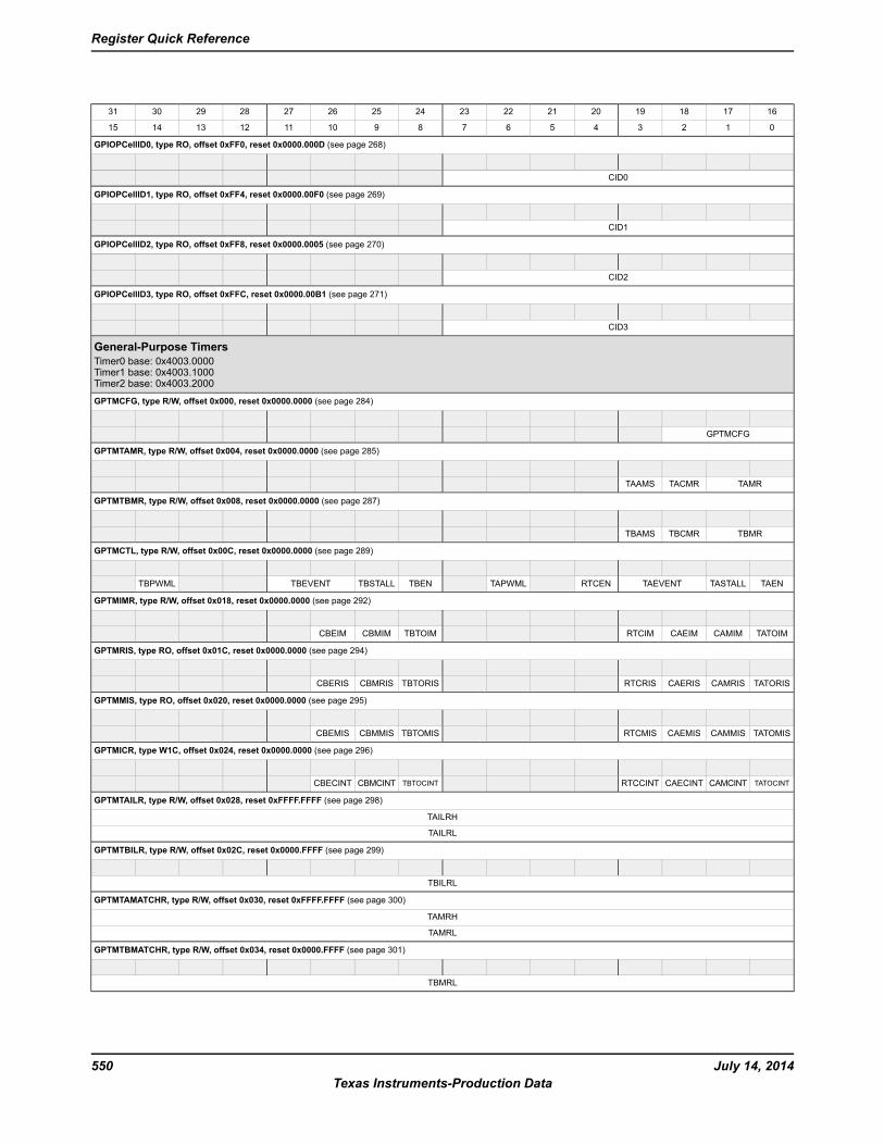
16171819202122232425262728293031
0123456789101112131415
GPIOPCellID0, type RO, offset 0xFF0, reset 0x0000.000D (see page 268)
CID0
GPIOPCellID1, type RO, offset 0xFF4, reset 0x0000.00F0 (see page 269)
CID1
GPIOPCellID2, type RO, offset 0xFF8, reset 0x0000.0005 (see page 270)
CID2
GPIOPCellID3, type RO, offset 0xFFC, reset 0x0000.00B1 (see page 271)
CID3
General-Purpose TimersTimer0 base: 0x4003.0000Timer1 base: 0x4003.1000Timer2 base: 0x4003.2000
GPTMCFG, type R/W, offset 0x000, reset 0x0000.0000 (see page 284)
GPTMCFG
GPTMTAMR, type R/W, offset 0x004, reset 0x0000.0000 (see page 285)
TAMRTACMRTAAMS
GPTMTBMR, type R/W, offset 0x008, reset 0x0000.0000 (see page 287)
TBMRTBCMRTBAMS
GPTMCTL, type R/W, offset 0x00C, reset 0x0000.0000 (see page 289)
TAENTASTALLTAEVENTRTCENTAPWMLTBENTBSTALLTBEVENTTBPWML
GPTMIMR, type R/W, offset 0x018, reset 0x0000.0000 (see page 292)
TATOIMCAMIMCAEIMRTCIMTBTOIMCBMIMCBEIM
GPTMRIS, type RO, offset 0x01C, reset 0x0000.0000 (see page 294)
TATORISCAMRISCAERISRTCRISTBTORISCBMRISCBERIS
GPTMMIS, type RO, offset 0x020, reset 0x0000.0000 (see page 295)
TATOMISCAMMISCAEMISRTCMISTBTOMISCBMMISCBEMIS
GPTMICR, type W1C, offset 0x024, reset 0x0000.0000 (see page 296)
TATOCINTCAMCINTCAECINTRTCCINTTBTOCINTCBMCINTCBECINT
GPTMTAILR, type R/W, offset 0x028, reset 0xFFFF.FFFF (see page 298)
TAILRH
TAILRL
GPTMTBILR, type R/W, offset 0x02C, reset 0x0000.FFFF (see page 299)
TBILRL
GPTMTAMATCHR, type R/W, offset 0x030, reset 0xFFFF.FFFF (see page 300)
TAMRH
TAMRL
GPTMTBMATCHR, type R/W, offset 0x034, reset 0x0000.FFFF (see page 301)
TBMRL
July 14, 2014550Texas Instruments-Production Data
Register Quick Reference
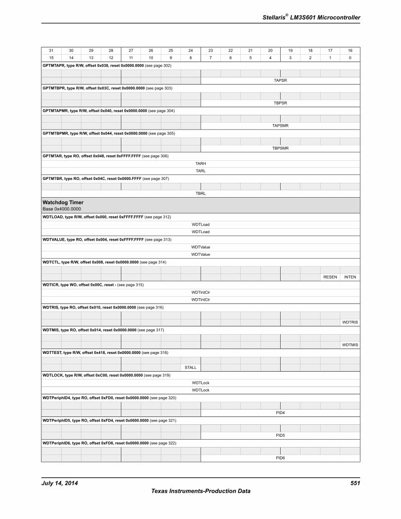
16171819202122232425262728293031
0123456789101112131415
GPTMTAPR, type R/W, offset 0x038, reset 0x0000.0000 (see page 302)
TAPSR
GPTMTBPR, type R/W, offset 0x03C, reset 0x0000.0000 (see page 303)
TBPSR
GPTMTAPMR, type R/W, offset 0x040, reset 0x0000.0000 (see page 304)
TAPSMR
GPTMTBPMR, type R/W, offset 0x044, reset 0x0000.0000 (see page 305)
TBPSMR
GPTMTAR, type RO, offset 0x048, reset 0xFFFF.FFFF (see page 306)
TARH
TARL
GPTMTBR, type RO, offset 0x04C, reset 0x0000.FFFF (see page 307)
TBRL
Watchdog TimerBase 0x4000.0000
WDTLOAD, type R/W, offset 0x000, reset 0xFFFF.FFFF (see page 312)
WDTLoad
WDTLoad
WDTVALUE, type RO, offset 0x004, reset 0xFFFF.FFFF (see page 313)
WDTValue
WDTValue
WDTCTL, type R/W, offset 0x008, reset 0x0000.0000 (see page 314)
INTENRESEN
WDTICR, type WO, offset 0x00C, reset - (see page 315)
WDTIntClr
WDTIntClr
WDTRIS, type RO, offset 0x010, reset 0x0000.0000 (see page 316)
WDTRIS
WDTMIS, type RO, offset 0x014, reset 0x0000.0000 (see page 317)
WDTMIS
WDTTEST, type R/W, offset 0x418, reset 0x0000.0000 (see page 318)
STALL
WDTLOCK, type R/W, offset 0xC00, reset 0x0000.0000 (see page 319)
WDTLock
WDTLock
WDTPeriphID4, type RO, offset 0xFD0, reset 0x0000.0000 (see page 320)
PID4
WDTPeriphID5, type RO, offset 0xFD4, reset 0x0000.0000 (see page 321)
PID5
WDTPeriphID6, type RO, offset 0xFD8, reset 0x0000.0000 (see page 322)
PID6
551July 14, 2014Texas Instruments-Production Data
Stellaris® LM3S601 Microcontroller
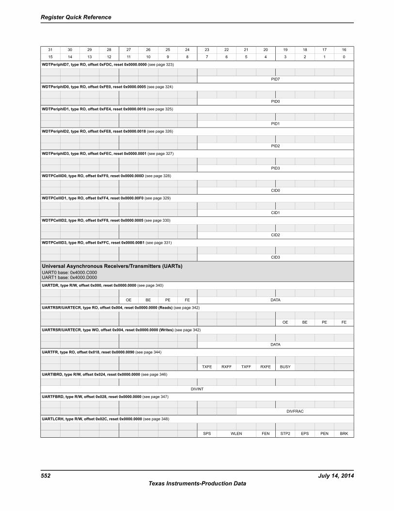
16171819202122232425262728293031
0123456789101112131415
WDTPeriphID7, type RO, offset 0xFDC, reset 0x0000.0000 (see page 323)
PID7
WDTPeriphID0, type RO, offset 0xFE0, reset 0x0000.0005 (see page 324)
PID0
WDTPeriphID1, type RO, offset 0xFE4, reset 0x0000.0018 (see page 325)
PID1
WDTPeriphID2, type RO, offset 0xFE8, reset 0x0000.0018 (see page 326)
PID2
WDTPeriphID3, type RO, offset 0xFEC, reset 0x0000.0001 (see page 327)
PID3
WDTPCellID0, type RO, offset 0xFF0, reset 0x0000.000D (see page 328)
CID0
WDTPCellID1, type RO, offset 0xFF4, reset 0x0000.00F0 (see page 329)
CID1
WDTPCellID2, type RO, offset 0xFF8, reset 0x0000.0005 (see page 330)
CID2
WDTPCellID3, type RO, offset 0xFFC, reset 0x0000.00B1 (see page 331)
CID3
Universal Asynchronous Receivers/Transmitters (UARTs)UART0 base: 0x4000.C000UART1 base: 0x4000.D000
UARTDR, type R/W, offset 0x000, reset 0x0000.0000 (see page 340)
DATAFEPEBEOE
UARTRSR/UARTECR, type RO, offset 0x004, reset 0x0000.0000 (Reads) (see page 342)
FEPEBEOE
UARTRSR/UARTECR, type WO, offset 0x004, reset 0x0000.0000 (Writes) (see page 342)
DATA
UARTFR, type RO, offset 0x018, reset 0x0000.0090 (see page 344)
BUSYRXFETXFFRXFFTXFE
UARTIBRD, type R/W, offset 0x024, reset 0x0000.0000 (see page 346)
DIVINT
UARTFBRD, type R/W, offset 0x028, reset 0x0000.0000 (see page 347)
DIVFRAC
UARTLCRH, type R/W, offset 0x02C, reset 0x0000.0000 (see page 348)
BRKPENEPSSTP2FENWLENSPS
July 14, 2014552Texas Instruments-Production Data
Register Quick Reference
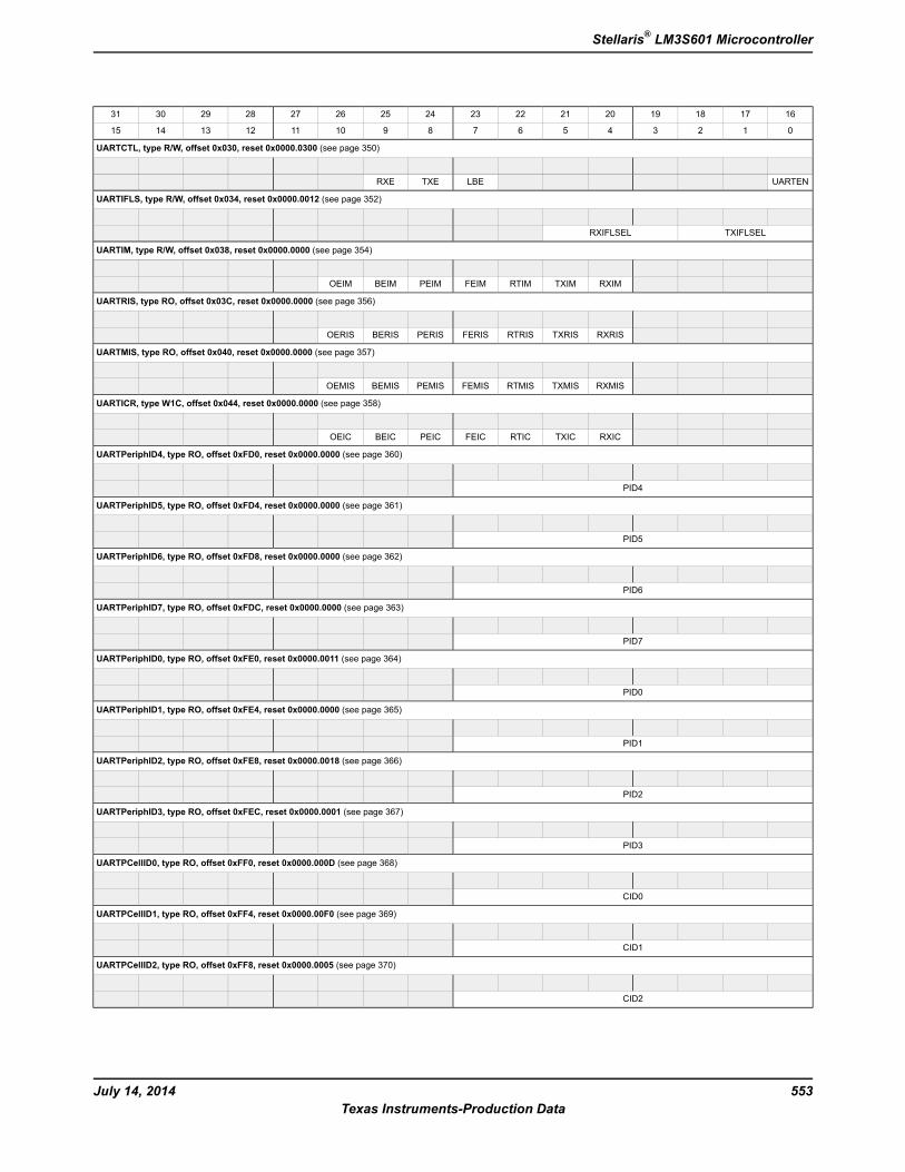
16171819202122232425262728293031
0123456789101112131415
UARTCTL, type R/W, offset 0x030, reset 0x0000.0300 (see page 350)
UARTENLBETXERXE
UARTIFLS, type R/W, offset 0x034, reset 0x0000.0012 (see page 352)
TXIFLSELRXIFLSEL
UARTIM, type R/W, offset 0x038, reset 0x0000.0000 (see page 354)
RXIMTXIMRTIMFEIMPEIMBEIMOEIM
UARTRIS, type RO, offset 0x03C, reset 0x0000.0000 (see page 356)
RXRISTXRISRTRISFERISPERISBERISOERIS
UARTMIS, type RO, offset 0x040, reset 0x0000.0000 (see page 357)
RXMISTXMISRTMISFEMISPEMISBEMISOEMIS
UARTICR, type W1C, offset 0x044, reset 0x0000.0000 (see page 358)
RXICTXICRTICFEICPEICBEICOEIC
UARTPeriphID4, type RO, offset 0xFD0, reset 0x0000.0000 (see page 360)
PID4
UARTPeriphID5, type RO, offset 0xFD4, reset 0x0000.0000 (see page 361)
PID5
UARTPeriphID6, type RO, offset 0xFD8, reset 0x0000.0000 (see page 362)
PID6
UARTPeriphID7, type RO, offset 0xFDC, reset 0x0000.0000 (see page 363)
PID7
UARTPeriphID0, type RO, offset 0xFE0, reset 0x0000.0011 (see page 364)
PID0
UARTPeriphID1, type RO, offset 0xFE4, reset 0x0000.0000 (see page 365)
PID1
UARTPeriphID2, type RO, offset 0xFE8, reset 0x0000.0018 (see page 366)
PID2
UARTPeriphID3, type RO, offset 0xFEC, reset 0x0000.0001 (see page 367)
PID3
UARTPCellID0, type RO, offset 0xFF0, reset 0x0000.000D (see page 368)
CID0
UARTPCellID1, type RO, offset 0xFF4, reset 0x0000.00F0 (see page 369)
CID1
UARTPCellID2, type RO, offset 0xFF8, reset 0x0000.0005 (see page 370)
CID2
553July 14, 2014Texas Instruments-Production Data
Stellaris® LM3S601 Microcontroller
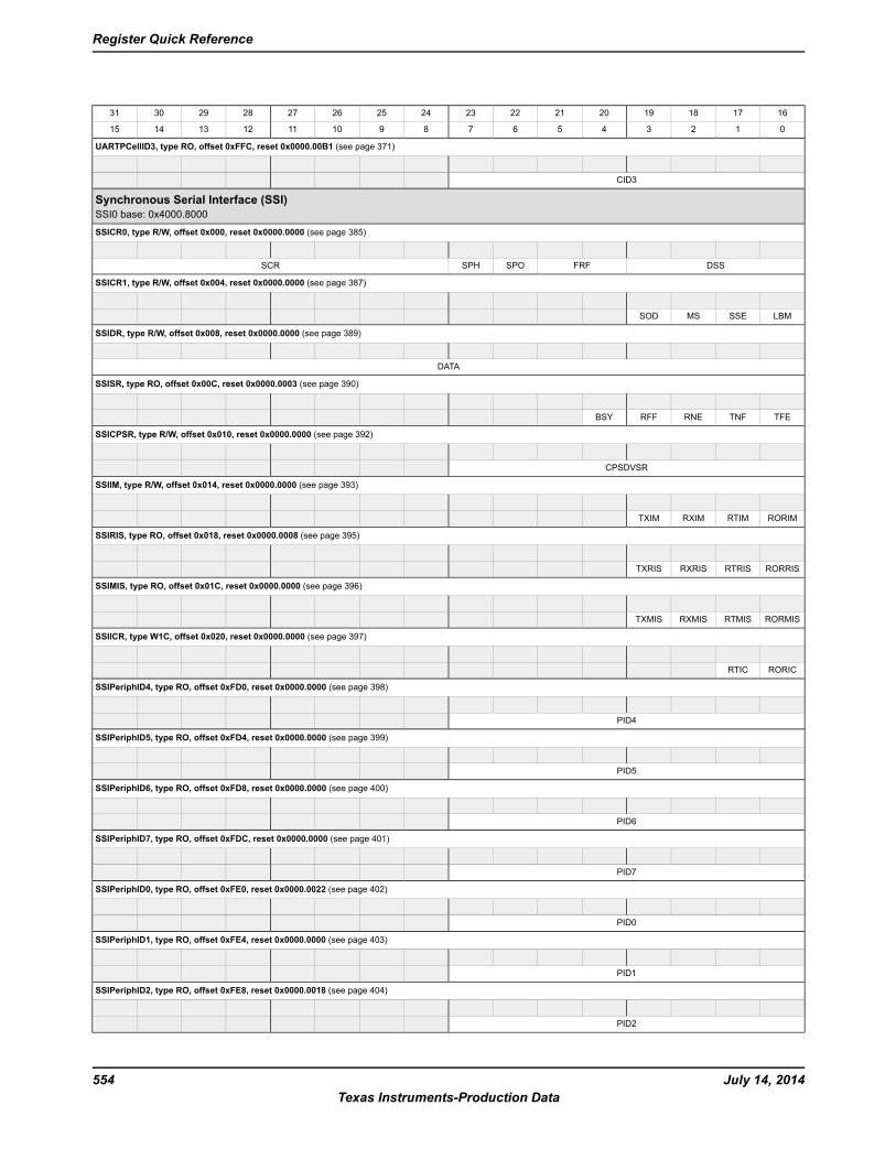
16171819202122232425262728293031
0123456789101112131415
UARTPCellID3, type RO, offset 0xFFC, reset 0x0000.00B1 (see page 371)
CID3
Synchronous Serial Interface (SSI)SSI0 base: 0x4000.8000
SSICR0, type R/W, offset 0x000, reset 0x0000.0000 (see page 385)
DSSFRFSPOSPHSCR
SSICR1, type R/W, offset 0x004, reset 0x0000.0000 (see page 387)
LBMSSEMSSOD
SSIDR, type R/W, offset 0x008, reset 0x0000.0000 (see page 389)
DATA
SSISR, type RO, offset 0x00C, reset 0x0000.0003 (see page 390)
TFETNFRNERFFBSY
SSICPSR, type R/W, offset 0x010, reset 0x0000.0000 (see page 392)
CPSDVSR
SSIIM, type R/W, offset 0x014, reset 0x0000.0000 (see page 393)
RORIMRTIMRXIMTXIM
SSIRIS, type RO, offset 0x018, reset 0x0000.0008 (see page 395)
RORRISRTRISRXRISTXRIS
SSIMIS, type RO, offset 0x01C, reset 0x0000.0000 (see page 396)
RORMISRTMISRXMISTXMIS
SSIICR, type W1C, offset 0x020, reset 0x0000.0000 (see page 397)
RORICRTIC
SSIPeriphID4, type RO, offset 0xFD0, reset 0x0000.0000 (see page 398)
PID4
SSIPeriphID5, type RO, offset 0xFD4, reset 0x0000.0000 (see page 399)
PID5
SSIPeriphID6, type RO, offset 0xFD8, reset 0x0000.0000 (see page 400)
PID6
SSIPeriphID7, type RO, offset 0xFDC, reset 0x0000.0000 (see page 401)
PID7
SSIPeriphID0, type RO, offset 0xFE0, reset 0x0000.0022 (see page 402)
PID0
SSIPeriphID1, type RO, offset 0xFE4, reset 0x0000.0000 (see page 403)
PID1
SSIPeriphID2, type RO, offset 0xFE8, reset 0x0000.0018 (see page 404)
PID2
July 14, 2014554Texas Instruments-Production Data
Register Quick Reference
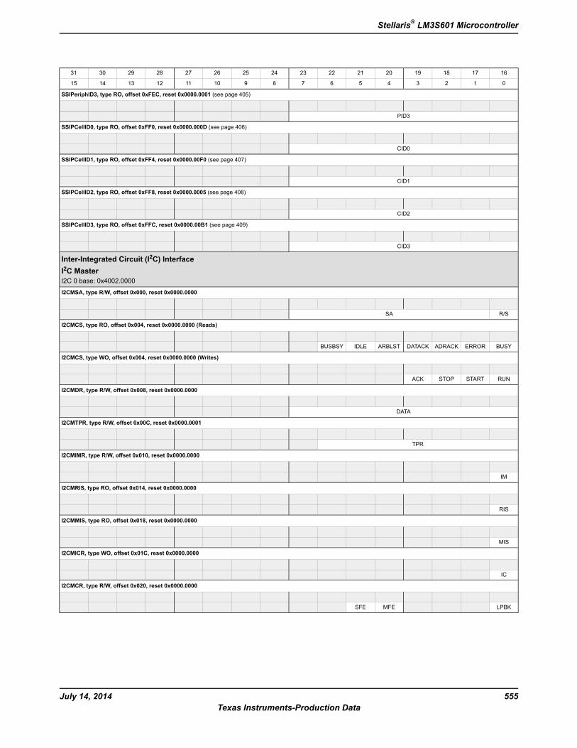
16171819202122232425262728293031
0123456789101112131415
SSIPeriphID3, type RO, offset 0xFEC, reset 0x0000.0001 (see page 405)
PID3
SSIPCellID0, type RO, offset 0xFF0, reset 0x0000.000D (see page 406)
CID0
SSIPCellID1, type RO, offset 0xFF4, reset 0x0000.00F0 (see page 407)
CID1
SSIPCellID2, type RO, offset 0xFF8, reset 0x0000.0005 (see page 408)
CID2
SSIPCellID3, type RO, offset 0xFFC, reset 0x0000.00B1 (see page 409)
CID3
Inter-Integrated Circuit (I2C) InterfaceI2C MasterI2C 0 base: 0x4002.0000
I2CMSA, type R/W, offset 0x000, reset 0x0000.0000
R/SSA
I2CMCS, type RO, offset 0x004, reset 0x0000.0000 (Reads)
BUSYERRORADRACKDATACKARBLSTIDLEBUSBSY
I2CMCS, type WO, offset 0x004, reset 0x0000.0000 (Writes)
RUNSTARTSTOPACK
I2CMDR, type R/W, offset 0x008, reset 0x0000.0000
DATA
I2CMTPR, type R/W, offset 0x00C, reset 0x0000.0001
TPR
I2CMIMR, type R/W, offset 0x010, reset 0x0000.0000
IM
I2CMRIS, type RO, offset 0x014, reset 0x0000.0000
RIS
I2CMMIS, type RO, offset 0x018, reset 0x0000.0000
MIS
I2CMICR, type WO, offset 0x01C, reset 0x0000.0000
IC
I2CMCR, type R/W, offset 0x020, reset 0x0000.0000
LPBKMFESFE
555July 14, 2014Texas Instruments-Production Data
Stellaris® LM3S601 Microcontroller
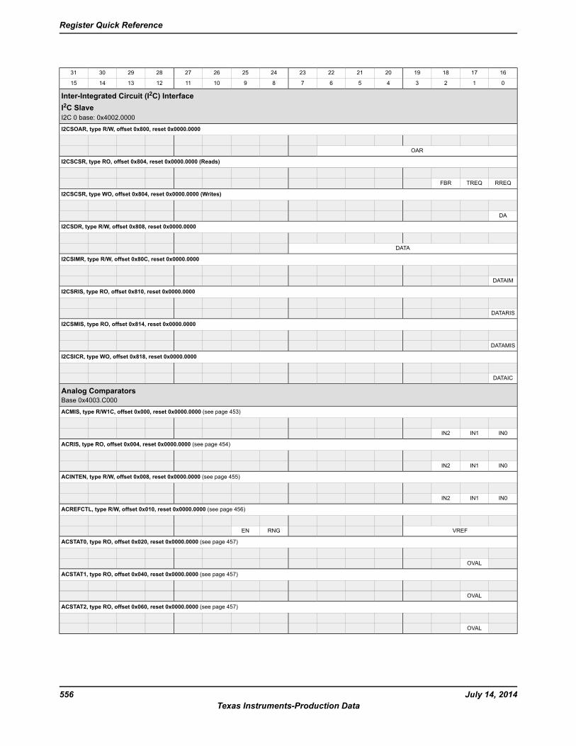
16171819202122232425262728293031
0123456789101112131415
Inter-Integrated Circuit (I2C) InterfaceI2C SlaveI2C 0 base: 0x4002.0000
I2CSOAR, type R/W, offset 0x800, reset 0x0000.0000
OAR
I2CSCSR, type RO, offset 0x804, reset 0x0000.0000 (Reads)
RREQTREQFBR
I2CSCSR, type WO, offset 0x804, reset 0x0000.0000 (Writes)
DA
I2CSDR, type R/W, offset 0x808, reset 0x0000.0000
DATA
I2CSIMR, type R/W, offset 0x80C, reset 0x0000.0000
DATAIM
I2CSRIS, type RO, offset 0x810, reset 0x0000.0000
DATARIS
I2CSMIS, type RO, offset 0x814, reset 0x0000.0000
DATAMIS
I2CSICR, type WO, offset 0x818, reset 0x0000.0000
DATAIC
Analog ComparatorsBase 0x4003.C000
ACMIS, type R/W1C, offset 0x000, reset 0x0000.0000 (see page 453)
IN0IN1IN2
ACRIS, type RO, offset 0x004, reset 0x0000.0000 (see page 454)
IN0IN1IN2
ACINTEN, type R/W, offset 0x008, reset 0x0000.0000 (see page 455)
IN0IN1IN2
ACREFCTL, type R/W, offset 0x010, reset 0x0000.0000 (see page 456)
VREFRNGEN
ACSTAT0, type RO, offset 0x020, reset 0x0000.0000 (see page 457)
OVAL
ACSTAT1, type RO, offset 0x040, reset 0x0000.0000 (see page 457)
OVAL
ACSTAT2, type RO, offset 0x060, reset 0x0000.0000 (see page 457)
OVAL
July 14, 2014556Texas Instruments-Production Data
Register Quick Reference
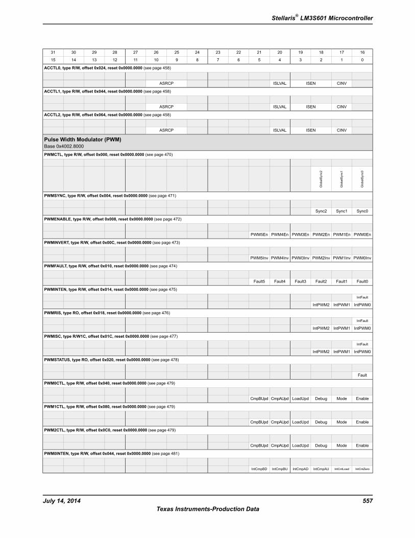
16171819202122232425262728293031
0123456789101112131415
ACCTL0, type R/W, offset 0x024, reset 0x0000.0000 (see page 458)
CINVISENISLVALASRCP
ACCTL1, type R/W, offset 0x044, reset 0x0000.0000 (see page 458)
CINVISENISLVALASRCP
ACCTL2, type R/W, offset 0x064, reset 0x0000.0000 (see page 458)
CINVISENISLVALASRCP
Pulse Width Modulator (PWM)Base 0x4002.8000
PWMCTL, type R/W, offset 0x000, reset 0x0000.0000 (see page 470)
GlobalSync0
GlobalSync1
GlobalSync2
PWMSYNC, type R/W, offset 0x004, reset 0x0000.0000 (see page 471)
Sync0Sync1Sync2
PWMENABLE, type R/W, offset 0x008, reset 0x0000.0000 (see page 472)
PWM0EnPWM1EnPWM2EnPWM3EnPWM4EnPWM5En
PWMINVERT, type R/W, offset 0x00C, reset 0x0000.0000 (see page 473)
PWM0InvPWM1InvPWM2InvPWM3InvPWM4InvPWM5Inv
PWMFAULT, type R/W, offset 0x010, reset 0x0000.0000 (see page 474)
Fault0Fault1Fault2Fault3Fault4Fault5
PWMINTEN, type R/W, offset 0x014, reset 0x0000.0000 (see page 475)
IntFault
IntPWM0IntPWM1IntPWM2
PWMRIS, type RO, offset 0x018, reset 0x0000.0000 (see page 476)
IntFault
IntPWM0IntPWM1IntPWM2
PWMISC, type R/W1C, offset 0x01C, reset 0x0000.0000 (see page 477)
IntFault
IntPWM0IntPWM1IntPWM2
PWMSTATUS, type RO, offset 0x020, reset 0x0000.0000 (see page 478)
Fault
PWM0CTL, type R/W, offset 0x040, reset 0x0000.0000 (see page 479)
EnableModeDebugLoadUpdCmpAUpdCmpBUpd
PWM1CTL, type R/W, offset 0x080, reset 0x0000.0000 (see page 479)
EnableModeDebugLoadUpdCmpAUpdCmpBUpd
PWM2CTL, type R/W, offset 0x0C0, reset 0x0000.0000 (see page 479)
EnableModeDebugLoadUpdCmpAUpdCmpBUpd
PWM0INTEN, type R/W, offset 0x044, reset 0x0000.0000 (see page 481)
IntCntZeroIntCntLoadIntCmpAUIntCmpADIntCmpBUIntCmpBD
557July 14, 2014Texas Instruments-Production Data
Stellaris® LM3S601 Microcontroller
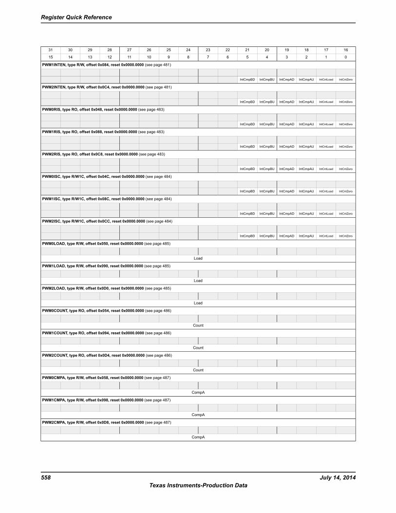
16171819202122232425262728293031
0123456789101112131415
PWM1INTEN, type R/W, offset 0x084, reset 0x0000.0000 (see page 481)
IntCntZeroIntCntLoadIntCmpAUIntCmpADIntCmpBUIntCmpBD
PWM2INTEN, type R/W, offset 0x0C4, reset 0x0000.0000 (see page 481)
IntCntZeroIntCntLoadIntCmpAUIntCmpADIntCmpBUIntCmpBD
PWM0RIS, type RO, offset 0x048, reset 0x0000.0000 (see page 483)
IntCntZeroIntCntLoadIntCmpAUIntCmpADIntCmpBUIntCmpBD
PWM1RIS, type RO, offset 0x088, reset 0x0000.0000 (see page 483)
IntCntZeroIntCntLoadIntCmpAUIntCmpADIntCmpBUIntCmpBD
PWM2RIS, type RO, offset 0x0C8, reset 0x0000.0000 (see page 483)
IntCntZeroIntCntLoadIntCmpAUIntCmpADIntCmpBUIntCmpBD
PWM0ISC, type R/W1C, offset 0x04C, reset 0x0000.0000 (see page 484)
IntCntZeroIntCntLoadIntCmpAUIntCmpADIntCmpBUIntCmpBD
PWM1ISC, type R/W1C, offset 0x08C, reset 0x0000.0000 (see page 484)
IntCntZeroIntCntLoadIntCmpAUIntCmpADIntCmpBUIntCmpBD
PWM2ISC, type R/W1C, offset 0x0CC, reset 0x0000.0000 (see page 484)
IntCntZeroIntCntLoadIntCmpAUIntCmpADIntCmpBUIntCmpBD
PWM0LOAD, type R/W, offset 0x050, reset 0x0000.0000 (see page 485)
Load
PWM1LOAD, type R/W, offset 0x090, reset 0x0000.0000 (see page 485)
Load
PWM2LOAD, type R/W, offset 0x0D0, reset 0x0000.0000 (see page 485)
Load
PWM0COUNT, type RO, offset 0x054, reset 0x0000.0000 (see page 486)
Count
PWM1COUNT, type RO, offset 0x094, reset 0x0000.0000 (see page 486)
Count
PWM2COUNT, type RO, offset 0x0D4, reset 0x0000.0000 (see page 486)
Count
PWM0CMPA, type R/W, offset 0x058, reset 0x0000.0000 (see page 487)
CompA
PWM1CMPA, type R/W, offset 0x098, reset 0x0000.0000 (see page 487)
CompA
PWM2CMPA, type R/W, offset 0x0D8, reset 0x0000.0000 (see page 487)
CompA
July 14, 2014558Texas Instruments-Production Data
Register Quick Reference
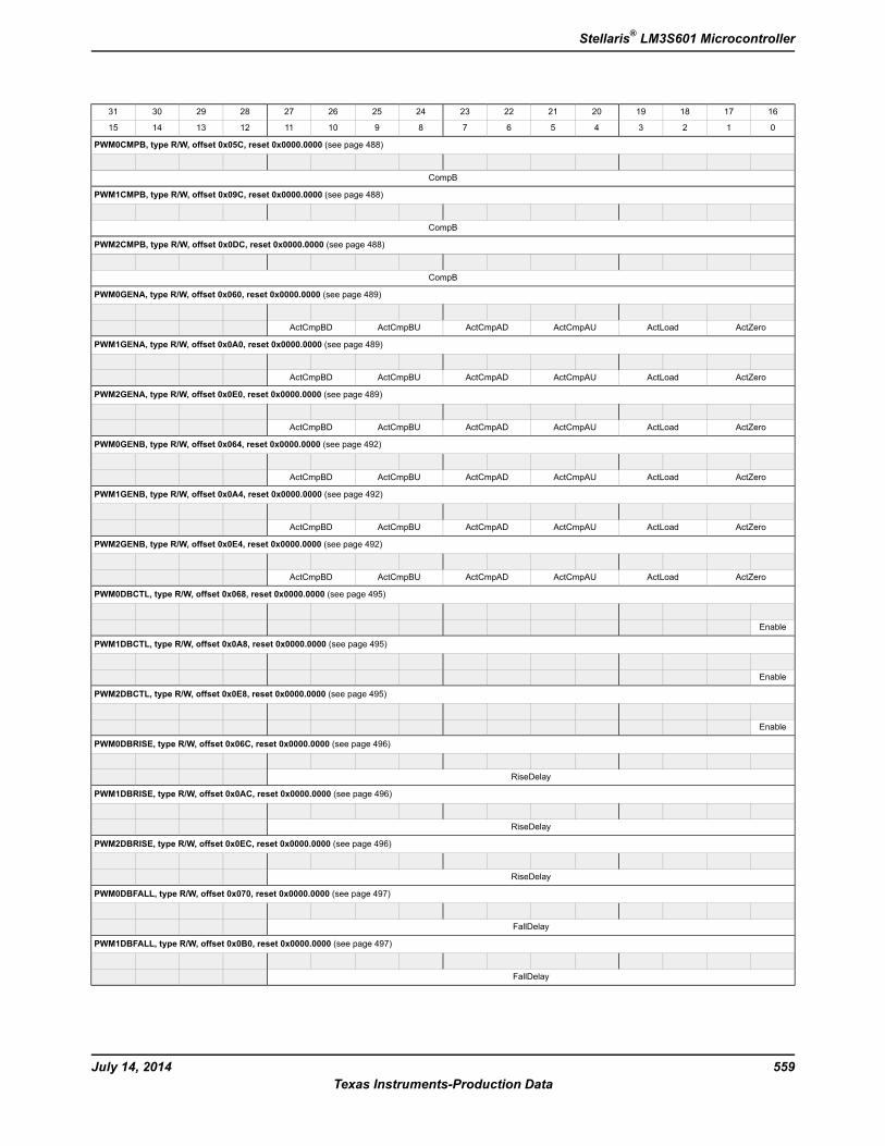
16171819202122232425262728293031
0123456789101112131415
PWM0CMPB, type R/W, offset 0x05C, reset 0x0000.0000 (see page 488)
CompB
PWM1CMPB, type R/W, offset 0x09C, reset 0x0000.0000 (see page 488)
CompB
PWM2CMPB, type R/W, offset 0x0DC, reset 0x0000.0000 (see page 488)
CompB
PWM0GENA, type R/W, offset 0x060, reset 0x0000.0000 (see page 489)
ActZeroActLoadActCmpAUActCmpADActCmpBUActCmpBD
PWM1GENA, type R/W, offset 0x0A0, reset 0x0000.0000 (see page 489)
ActZeroActLoadActCmpAUActCmpADActCmpBUActCmpBD
PWM2GENA, type R/W, offset 0x0E0, reset 0x0000.0000 (see page 489)
ActZeroActLoadActCmpAUActCmpADActCmpBUActCmpBD
PWM0GENB, type R/W, offset 0x064, reset 0x0000.0000 (see page 492)
ActZeroActLoadActCmpAUActCmpADActCmpBUActCmpBD
PWM1GENB, type R/W, offset 0x0A4, reset 0x0000.0000 (see page 492)
ActZeroActLoadActCmpAUActCmpADActCmpBUActCmpBD
PWM2GENB, type R/W, offset 0x0E4, reset 0x0000.0000 (see page 492)
ActZeroActLoadActCmpAUActCmpADActCmpBUActCmpBD
PWM0DBCTL, type R/W, offset 0x068, reset 0x0000.0000 (see page 495)
Enable
PWM1DBCTL, type R/W, offset 0x0A8, reset 0x0000.0000 (see page 495)
Enable
PWM2DBCTL, type R/W, offset 0x0E8, reset 0x0000.0000 (see page 495)
Enable
PWM0DBRISE, type R/W, offset 0x06C, reset 0x0000.0000 (see page 496)
RiseDelay
PWM1DBRISE, type R/W, offset 0x0AC, reset 0x0000.0000 (see page 496)
RiseDelay
PWM2DBRISE, type R/W, offset 0x0EC, reset 0x0000.0000 (see page 496)
RiseDelay
PWM0DBFALL, type R/W, offset 0x070, reset 0x0000.0000 (see page 497)
FallDelay
PWM1DBFALL, type R/W, offset 0x0B0, reset 0x0000.0000 (see page 497)
FallDelay
559July 14, 2014Texas Instruments-Production Data
Stellaris® LM3S601 Microcontroller
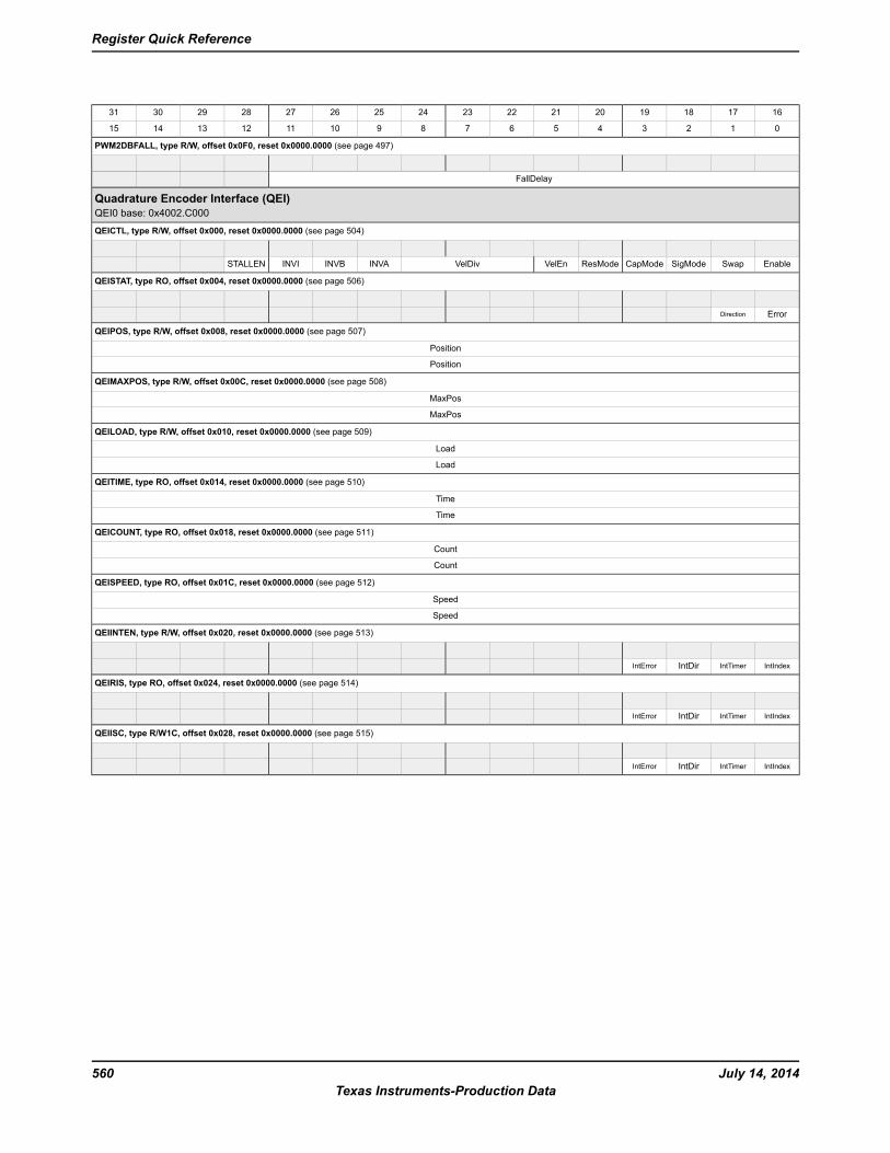
16171819202122232425262728293031
0123456789101112131415
PWM2DBFALL, type R/W, offset 0x0F0, reset 0x0000.0000 (see page 497)
FallDelay
Quadrature Encoder Interface (QEI)QEI0 base: 0x4002.C000
QEICTL, type R/W, offset 0x000, reset 0x0000.0000 (see page 504)
EnableSwapSigModeCapModeResModeVelEnVelDivINVAINVBINVISTALLEN
QEISTAT, type RO, offset 0x004, reset 0x0000.0000 (see page 506)
ErrorDirection
QEIPOS, type R/W, offset 0x008, reset 0x0000.0000 (see page 507)
Position
Position
QEIMAXPOS, type R/W, offset 0x00C, reset 0x0000.0000 (see page 508)
MaxPos
MaxPos
QEILOAD, type R/W, offset 0x010, reset 0x0000.0000 (see page 509)
Load
Load
QEITIME, type RO, offset 0x014, reset 0x0000.0000 (see page 510)
Time
Time
QEICOUNT, type RO, offset 0x018, reset 0x0000.0000 (see page 511)
Count
Count
QEISPEED, type RO, offset 0x01C, reset 0x0000.0000 (see page 512)
Speed
Speed
QEIINTEN, type R/W, offset 0x020, reset 0x0000.0000 (see page 513)
IntIndexIntTimerIntDirIntError
QEIRIS, type RO, offset 0x024, reset 0x0000.0000 (see page 514)
IntIndexIntTimerIntDirIntError
QEIISC, type R/W1C, offset 0x028, reset 0x0000.0000 (see page 515)
IntIndexIntTimerIntDirIntError
July 14, 2014560Texas Instruments-Production Data
Register Quick Reference
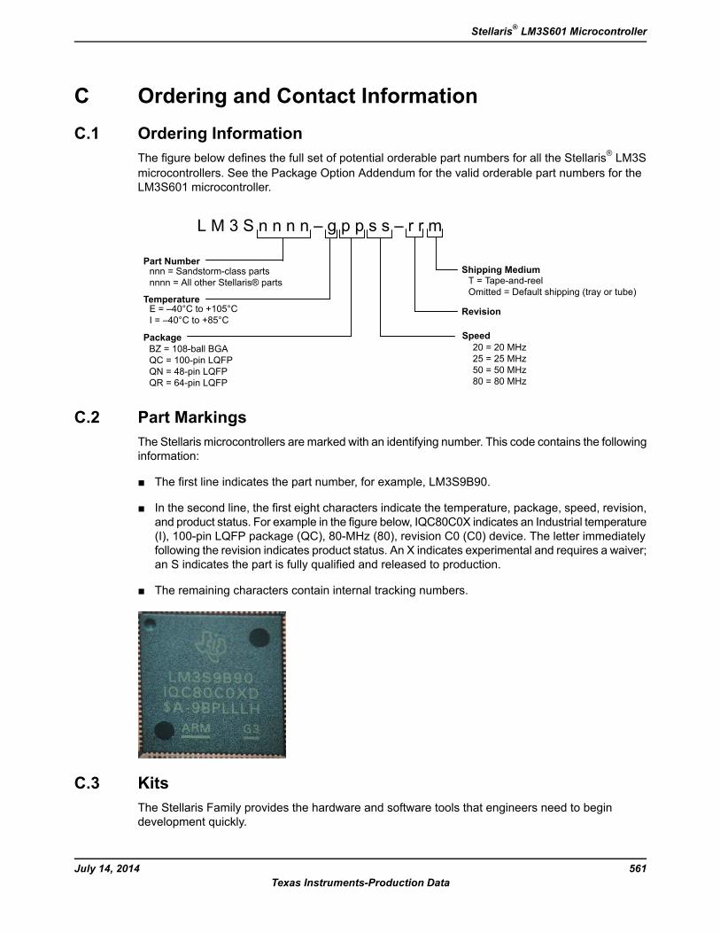
C Ordering and Contact InformationC.1 Ordering Information
The figure below defines the full set of potential orderable part numbers for all the Stellaris® LM3Smicrocontrollers. See the Package Option Addendum for the valid orderable part numbers for theLM3S601 microcontroller.
L M 3 S n n n n – g p p s s – r r m
Part Number
Temperature
Package Speed
Revision
Shipping Medium
E = –40°C to +105°CI = –40°C to +85°C
T = Tape-and-reelOmitted = Default shipping (tray or tube)
BZ = 108-ball BGAQC = 100-pin LQFPQN = 48-pin LQFPQR = 64-pin LQFP
20 = 20 MHz25 = 25 MHz50 = 50 MHz80 = 80 MHz
nnn = Sandstorm-class partsnnnn = All other Stellaris® parts
C.2 Part MarkingsThe Stellaris microcontrollers are marked with an identifying number. This code contains the followinginformation:
The first line indicates the part number, for example, LM3S9B90.
In the second line, the first eight characters indicate the temperature, package, speed, revision,and product status. For example in the figure below, IQC80C0X indicates an Industrial temperature(I), 100-pin LQFP package (QC), 80-MHz (80), revision C0 (C0) device. The letter immediatelyfollowing the revision indicates product status. An X indicates experimental and requires a waiver;an S indicates the part is fully qualified and released to production.
The remaining characters contain internal tracking numbers.
C.3 KitsThe Stellaris Family provides the hardware and software tools that engineers need to begindevelopment quickly.
561July 14, 2014Texas Instruments-Production Data
Stellaris® LM3S601 Microcontroller
Reference Design Kits accelerate product development by providing ready-to-run hardware andcomprehensive documentation including hardware design files
Evaluation Kits provide a low-cost and effective means of evaluating Stellaris microcontrollersbefore purchase
Development Kits provide you with all the tools you need to develop and prototype embeddedapplications right out of the box
See the website at www.ti.com/stellaris for the latest tools available, or ask your distributor.
C.4 Support InformationFor support on Stellaris products, contact the TI Worldwide Product Information Center nearest you:http://www-k.ext.ti.com/sc/technical-support/product-information-centers.htm.
July 14, 2014562Texas Instruments-Production Data
Ordering and Contact Information
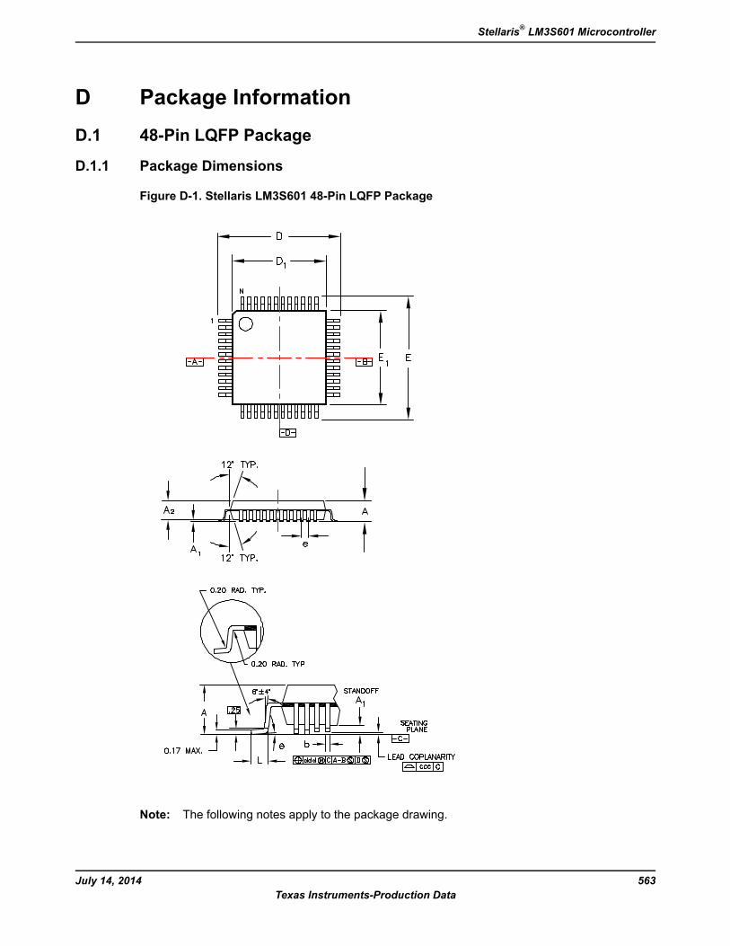
D Package InformationD.1 48-Pin LQFP Package
D.1.1 Package Dimensions
Figure D-1. Stellaris LM3S601 48-Pin LQFP Package
Note: The following notes apply to the package drawing.
563July 14, 2014Texas Instruments-Production Data
Stellaris® LM3S601 Microcontroller
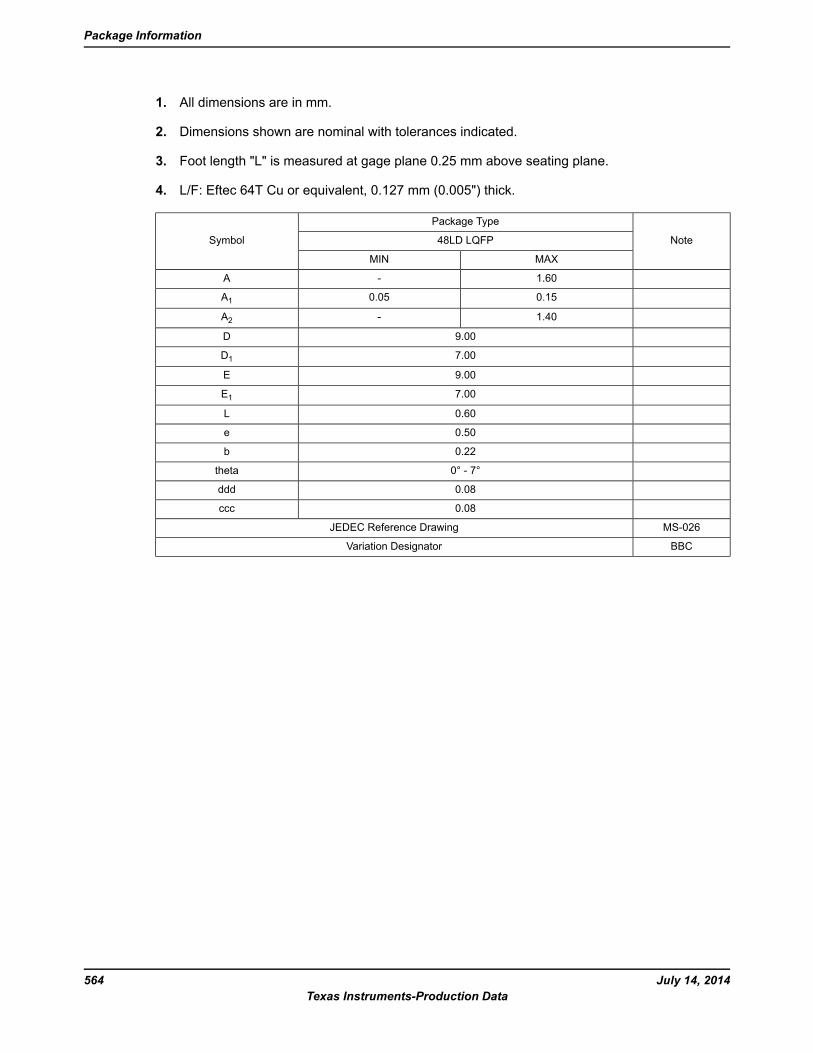
1. All dimensions are in mm.
2. Dimensions shown are nominal with tolerances indicated.
3. Foot length "L" is measured at gage plane 0.25 mm above seating plane.
4. L/F: Eftec 64T Cu or equivalent, 0.127 mm (0.005") thick.
Note
Package Type
Symbol 48LD LQFP
MAXMIN
1.60-A
0.150.05A11.40-A2
9.00D
7.00D1
9.00E
7.00E10.60L
0.50e
0.22b
0° - 7°theta
0.08ddd
0.08ccc
MS-026JEDEC Reference Drawing
BBCVariation Designator
July 14, 2014564Texas Instruments-Production Data
Package Information
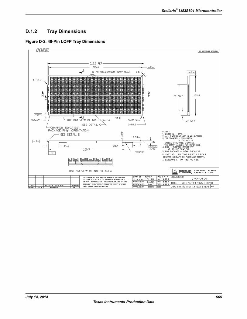
D.1.2 Tray Dimensions
Figure D-2. 48-Pin LQFP Tray Dimensions
565July 14, 2014Texas Instruments-Production Data
Stellaris® LM3S601 Microcontroller
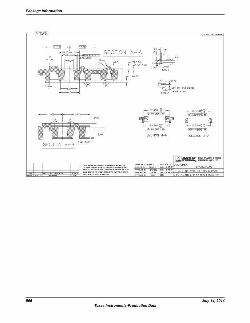
July 14, 2014566Texas Instruments-Production Data
Package Information
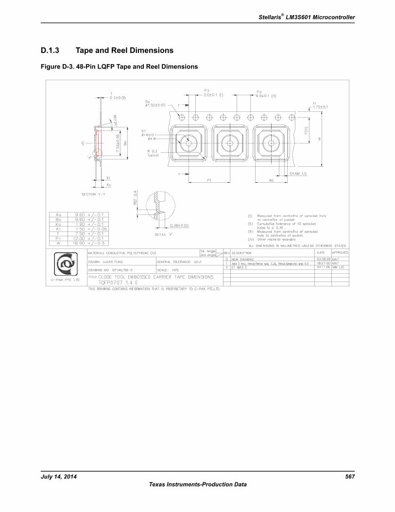
D.1.3 Tape and Reel Dimensions
Figure D-3. 48-Pin LQFP Tape and Reel Dimensions
567July 14, 2014Texas Instruments-Production Data
Stellaris® LM3S601 Microcontroller

IMPORTANT NOTICE AND DISCLAIMERTI PROVIDES TECHNICAL AND RELIABILITY DATA (INCLUDING DATASHEETS), DESIGN RESOURCES (INCLUDING REFERENCEDESIGNS), APPLICATION OR OTHER DESIGN ADVICE, WEB TOOLS, SAFETY INFORMATION, AND OTHER RESOURCES “AS IS”AND WITH ALL FAULTS, AND DISCLAIMS ALL WARRANTIES, EXPRESS AND IMPLIED, INCLUDING WITHOUT LIMITATION ANYIMPLIED WARRANTIES OF MERCHANTABILITY, FITNESS FOR A PARTICULAR PURPOSE OR NON-INFRINGEMENT OF THIRDPARTY INTELLECTUAL PROPERTY RIGHTS.These resources are intended for skilled developers designing with TI products. You are solely responsible for (1) selecting the appropriateTI products for your application, (2) designing, validating and testing your application, and (3) ensuring your application meets applicablestandards, and any other safety, security, or other requirements. These resources are subject to change without notice. TI grants youpermission to use these resources only for development of an application that uses the TI products described in the resource. Otherreproduction and display of these resources is prohibited. No license is granted to any other TI intellectual property right or to any third partyintellectual property right. TI disclaims responsibility for, and you will fully indemnify TI and its representatives against, any claims, damages,costs, losses, and liabilities arising out of your use of these resources.TI’s products are provided subject to TI’s Terms of Sale (https:www.ti.com/legal/termsofsale.html) or other applicable terms available eitheron ti.com or provided in conjunction with such TI products. TI’s provision of these resources does not expand or otherwise alter TI’sapplicable warranties or warranty disclaimers for TI products.IMPORTANT NOTICE
Mailing Address: Texas Instruments, Post Office Box 655303, Dallas, Texas 75265Copyright © 2021, Texas Instruments Incorporated