Embed Size (px)
Citation preview
Studies of Magnetic Logic Devices
by
Likun Hu
A thesis
presented to the University of Waterloo
in fulfillment of the
thesis requirement for the degree of
Master of Applied Science
in
Electrical and Computer Engineering
Waterloo, Ontario, Canada, 2012
c© Likun Hu 2012

I hereby declare that I am the sole author of this thesis. This is a true copy of the thesis,
including any required final revisions, as accepted by my examiners.
I understand that my thesis may be made electronically available to the public.
ii
Abstract
Magnetic nanoscale devices have shown great promise in both research and industry.
Magnetic nanostructures have potential for non-volatile data storage applications, recon-
figurable logic devices, biomedical devices and many more.
The S-state magnetic element is one of the promising structures for non-volatile data
storage applications and reconfigurable logic devices. It is a single-layer logic element that
can be integrated in magnetoresistive structures. We present a detailed micromagnetic
analysis of the geometrical parameter space in which the logic operation is carried out.
The influence of imperfections, such as sidewall roughness and roundness of the edge is
investigated.
Magnetic nanowires are highly attractive materials that has potential for applications
in ultrahigh magnetic recording, logic operation devices, and micromagnetic and spin-
tronic sensors. To utilize applications, manipulation and assembly of nanowires into or-
dered structures is needed. Magnetic self-alignment is a facile technique for assembling
nanowires into hierarchical structures. In my thesis, I focus on synthesizing and assem-
bling nickel nanowires. The magnetic behaviour of a single nickel nanowire with 200 nm
diameter is investigated in micromagnetic simulations. Nickel nanowires with Au caps at
the ends were synthesized by electrochemical deposition into nanopores in alumina tem-
plates. One-dimensional alignment, which forms chains and two-dimensional alignment,
which forms T-junctions as well as cross-junctions are demonstrated. Attempts to achieve
three-dimensional alignment were not successful yet. I will discuss strategies to improve
the alignment process.
iii

Acknowledgements
First and foremost, I would like to sincerely express my gratitude to my supervisor,
Professor Thorsten Hesjedal, for his support and guidance. Without his inspiration, pre-
cious advise and enormous patience, I would not be able to finish my graduate study in
University of Waterloo. His attitude towards research, family and students inspired me
to think differently about my work, study and life, and it will influence me for years to
come. Without Professor Hesjedal’s support and encouragement, I would not have been
able to obtain the opportunity to study in this field and would not have been able to gain
valuable industrial experiences. The entire graduate experience has been fantastic and
unforgettable thanks to my supervisor.
I would like to acknowledge Professor Siva Sivoththaman for his help and support on
my program completion.
I would alse like to thank kindly the members of our research group: Randy Fagan,
James Mracek and Daniel Russo for their help with my research.
Finally, my deepest gratitude goes to my parents for their support and encouragement.
iv
Contents
List of Tables viii
List of Figures x
1 Introduction 1
1.1 Motivation . . . . . . . . . . . . . . . . . . . . . . . . . . . . . . . . . . . . 1
1.2 Magnetic Logic Devices . . . . . . . . . . . . . . . . . . . . . . . . . . . . . 2
1.3 Magnetic Nanowire Assemblies . . . . . . . . . . . . . . . . . . . . . . . . . 6
2 Micromagnetics 7
2.1 Introduction . . . . . . . . . . . . . . . . . . . . . . . . . . . . . . . . . . . 7
2.2 Energy Contributions in Micromagnetics . . . . . . . . . . . . . . . . . . . 8
2.2.1 Exchange Energy . . . . . . . . . . . . . . . . . . . . . . . . . . . . 8
2.2.2 Anisotropy Energy . . . . . . . . . . . . . . . . . . . . . . . . . . . 10
2.2.3 Zeeman Energy . . . . . . . . . . . . . . . . . . . . . . . . . . . . . 11
2.2.4 Stray Field Energy . . . . . . . . . . . . . . . . . . . . . . . . . . . 11
2.3 Micromagnetic Equations . . . . . . . . . . . . . . . . . . . . . . . . . . . 12
v
2.4 Micromagnetic Simulations . . . . . . . . . . . . . . . . . . . . . . . . . . . 13
2.5 Micromagnetic Simulators . . . . . . . . . . . . . . . . . . . . . . . . . . . 15
2.6 Micromagnetic Systems . . . . . . . . . . . . . . . . . . . . . . . . . . . . . 16
2.6.1 Hysteresis Loops . . . . . . . . . . . . . . . . . . . . . . . . . . . . 16
2.6.2 Ferromagnetic Domains . . . . . . . . . . . . . . . . . . . . . . . . 17
3 Micromagnetic Investigation of the S-State Reconfigurable Logic Ele-
ment 19
3.1 S-State Reconfigurable Logic Element . . . . . . . . . . . . . . . . . . . . . 20
3.2 Simulation Setup . . . . . . . . . . . . . . . . . . . . . . . . . . . . . . . . 25
3.3 Remanent Magnetization Patterns in Rectangular Prisms . . . . . . . . . . 27
3.4 Influence of the Rectangular Aspect Ratio a:b . . . . . . . . . . . . . . . . 31
3.5 Study of the Appendage Size . . . . . . . . . . . . . . . . . . . . . . . . . . 33
3.6 Study of Imperfections . . . . . . . . . . . . . . . . . . . . . . . . . . . . . 35
3.7 Optimization of the Biasing Field . . . . . . . . . . . . . . . . . . . . . . . 39
3.8 Discussion . . . . . . . . . . . . . . . . . . . . . . . . . . . . . . . . . . . . 42
3.9 Summary . . . . . . . . . . . . . . . . . . . . . . . . . . . . . . . . . . . . 44
4 Self-assembly of Magnetic Nanowires 45
4.1 Introduction . . . . . . . . . . . . . . . . . . . . . . . . . . . . . . . . . . . 45
4.2 Simulation of Individual Nickel Nanowires . . . . . . . . . . . . . . . . . . 46
4.2.1 Relaxation and Reversal Dynamics of Single Nickel Nanowire . . . . 46
4.3 Nanowire Synthesis . . . . . . . . . . . . . . . . . . . . . . . . . . . . . . . 53
vi
4.4 Two-Dimensional Alignment . . . . . . . . . . . . . . . . . . . . . . . . . . 56
4.5 Three-Dimensional Alignment . . . . . . . . . . . . . . . . . . . . . . . . . 62
4.6 Summary . . . . . . . . . . . . . . . . . . . . . . . . . . . . . . . . . . . . 65
5 Conclusions and Future Work 66
5.1 Summary . . . . . . . . . . . . . . . . . . . . . . . . . . . . . . . . . . . . 66
5.2 Future Work . . . . . . . . . . . . . . . . . . . . . . . . . . . . . . . . . . . 67
Bibliography 77
vii

List of Tables
1.1 Truth-table of the majority gate geometry . . . . . . . . . . . . . . . . . . 5
3.1 Influence of roughness and edge roundness on the coercive field . . . . . . . 38
viii
List of Figures
1.1 Historic microprocessor clock frequency statistics . . . . . . . . . . . . . . 2
1.2 Magnetic majority gate . . . . . . . . . . . . . . . . . . . . . . . . . . . . . 4
2.1 Time evolution of the magnetization in a magnetic field . . . . . . . . . . . 14
2.2 Schematic plot of hysteresis loop . . . . . . . . . . . . . . . . . . . . . . . . 17
3.1 S-shaped magnetic element: shape and parameters . . . . . . . . . . . . . . 22
3.2 S-Shaped Magnetic logic element: remanent magnetization, coercive field
shifts, and truth table. . . . . . . . . . . . . . . . . . . . . . . . . . . . . . 24
3.3 Remanent magnetization of rectangular thin-film elements of dimensions a× b 28
3.4 Remanent magnetization of rectangular thin-film elements of dimensions
a× b with fix appendage size (c× d = 40 nm×50 nm) . . . . . . . . . . . . 30
3.5 Plot of coercive field and remanent magnetization as a function of a/b . . . 32
3.6 Plot of coercive field and remanent magnetization dependency on appendage
overall area and aspect ratio . . . . . . . . . . . . . . . . . . . . . . . . . . 34
3.7 Illustration of S-shaped elements with sidewall roundness and roughness,
and their hysteresis loop . . . . . . . . . . . . . . . . . . . . . . . . . . . . 36
ix
3.8 Plots of the shift of the coercive field, ∆Hc, as a function of rectangle form
factor and appendage form factor. . . . . . . . . . . . . . . . . . . . . . . . 40
4.1 Snapshots of the relaxation process starting from random initial magnetization 47
4.2 Remanent magnetization relaxed from saturated magnetization along z-axis 48
4.3 Magnetic reversal process . . . . . . . . . . . . . . . . . . . . . . . . . . . 50
4.4 Hysteresis plot of nickel nanowire with 200 nm diameter . . . . . . . . . . 52
4.5 Scanning electron micrograph of Au-Ni-Au nanowires . . . . . . . . . . . . 55
4.6 Optical microscope images of 1D and 2D alignments . . . . . . . . . . . . . 59
4.7 Alignment mechanism . . . . . . . . . . . . . . . . . . . . . . . . . . . . . 61
4.8 Dynamic viscosity of water . . . . . . . . . . . . . . . . . . . . . . . . . . . 64
x
Chapter 1
Introduction
1.1 Motivation
The silicon microchip has been one of the most impressive pieces of engineering ever made.
Moore’s law introduced by Gordon Moore in 1965 describes a long term trend that the
number of transistors that can be placed inexpensively on an integrated circuit that dou-
bles approximately every two years [1]. This prediction has lasted for nearly 45 years.
The capabilities of many digital electronic devices are strongly linked to Moore’s Law:
processing speed, memory capacity, sensors, etc.
At present, researchers are still trying to exploit the properties of semiconductors and
production processes. Like all other technologies, however, it will stop growing exponen-
tially and enter the realm of diminishment. In recent years, there is a clear trend that the
performance scaling of uniprocessor is saturating, so we can no longer follow this doubling
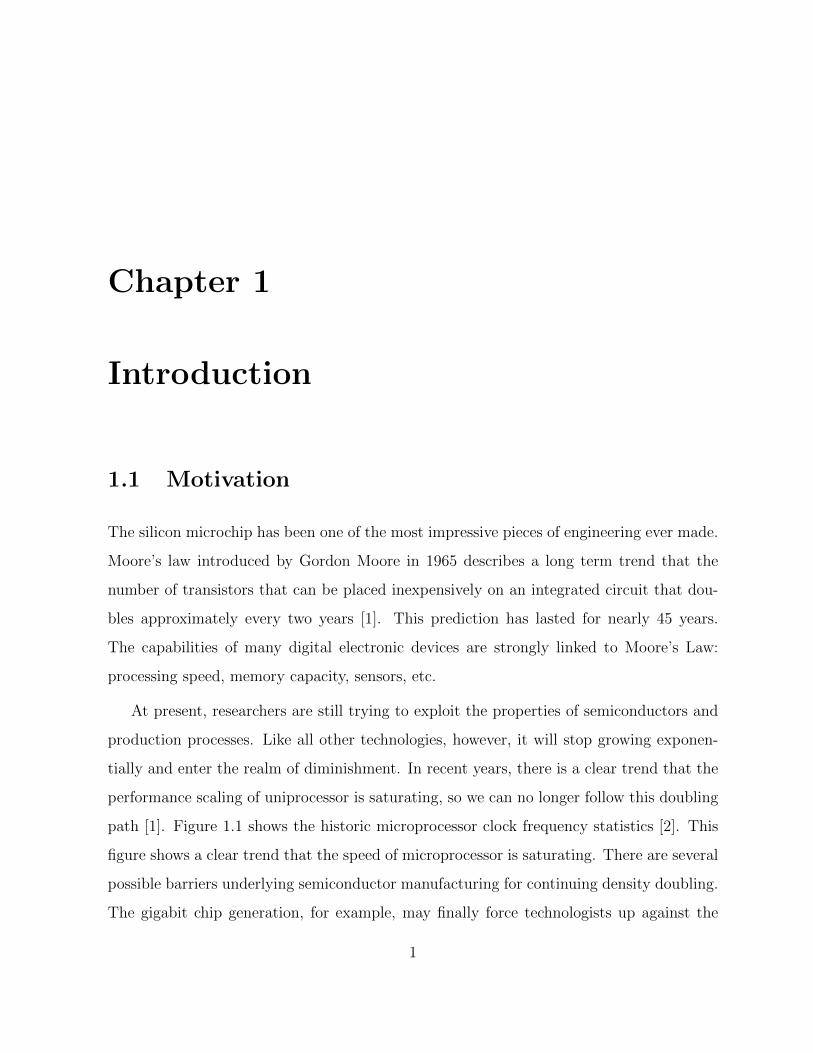
path [1]. Figure 1.1 shows the historic microprocessor clock frequency statistics [2]. This
figure shows a clear trend that the speed of microprocessor is saturating. There are several
possible barriers underlying semiconductor manufacturing for continuing density doubling.
The gigabit chip generation, for example, may finally force technologists up against the
1
Figure 1.1: Historic microprocessor clock frequency statistics [2]. Power consumption
has been increasing by about two orders of magnitude for last two decades. (PA is the
abbreviation for Precision Architecture)
limits of optical lithography. At the same time, the cost will rise exponentially along with
component densities, and it is possible that the price per transistor will bottom out, means
that there will be no profit in making transistors smaller. In fact, economics may constrain
Moore’s Law before physics does [1].
1.2 Magnetic Logic Devices
Magnetic logic devices have been widely explored for memory and sensor applications.
These devices make it possible to achieve programmable and nonvolatile logic functional-
ities [3]. Using ferromagnetic materials for logic operation is not a new idea, and it was
commercialized over 60 years ago [4]. Ferromagnetic materials have also been considered
2
for applications of logic operation in digital computers since the appearance of the first
magnetic memory device. Hans Gschwind summarized the reasons why magnetic logic
devices are rather attractive to the computer designer [5]:
• They possess the nonvolatility of the stored information.
• They require in most applications no power other than the power to switch their
states, which can greatly reduce power consumption.
• They have the potential to perform all required operations for computer at room
temperature, i.e., full logic function, storage and amplification.
Magnetic logic devices are experiencing a comeback [3]. Programmable logic functions may
be implemented as conventional programmed logic arrays that use the magnetic devices
as the nonvolatile programming elements or as arrays of universal logic gates. So the core
logic functions are magnetically programmed. The key feature of ferromagnetic compo-
nents for logic operation is magnetic hysteresis, which describes the magnetization of the
components as a function of external magnetizing force and magnetization history. Nearly
all applications rely on particular aspects of hysteresis heavily [6].
Imre et al. [6] have experimentally demonstrated a universal logic gate based on mag-
netic structures. Its structure is based on the concept of cellular automata which are
networks of cells with rules that describe how neighboring cells interact. Figure 1.2(a)
shows the structure proposed by Imre. The magnetic state of nanomagnets ”A”, ”B”,
and ”C” can be set by some inputs; the majority logic operation will be performed by the
central nanomagnet ”M”; and the result can be transferred to the nanomagnet labelled
as ”out”. The overall cross-geometry can be schematically represented by the symbol in
Fig. 1.2(b) and the truth table is introduced in Tab. 1.2. The state of center nanomagnet
”M” takes the majority state of its three inputs and the output nanomagnet ”out” takes
the inverted state. From the truth table, if one of the three inputs constantly tied to logic
3
Figure 1.2: Magnetic majority gate. [7] (a) Majority gate geometry consists of elongated
nanomagnets. (b) Majority gate symbol.
1, then the gate performs the NOR operation. On the contrary, if one of the three inputs
tied permanently to logic 0, then the gate simply perform NAND operation. This single
gate proposed by Imre can performs both NAND and NOR operations.
All other types of Boolean logic gates, i.e., AND, OR, NOT, XOR, XNOR, can be
created from a suitable network of NAND gates, NOR gates, or the combination of the two.
Due to this property, NAND and NOR gates are sometimes called ”universal gates”. The
convenience of having a single universal gate gives the possibility of building programmable
logic hardware. The word ’programmable’ is used here to indicate that the actual function
of the gate can be reconfigured after the hardware has been built. By enabling users to
effectively create customized hardware, many different applications can be allowed in a
single chip, which reduces both cost and time. The ability to reconfigure logic is useful for
more than simple device prototyping [3].
4
A B C ABC M out
0 0 0 010 0 1
0 0 1 011 1 0
1 0 0 110 1 0
1 0 1 111 1 0
0 1 0 000 0 0
0 1 1 001 0 1
1 1 0 100 0 1
1 1 1 101 1 0
Table 1.1: Truth-table of the majority gate geometry
Another noteworthy feature of the magnetic majority gate is that it uses an adiabatic
switch scheme. The adiabatic switch scheme makes the energy barriers between discrete
data states gradually lowered and then raised again, which allows the system gradually
move from one computational state to another without wasting the energy like the con-
ventional architectures [8].
One of the challenges of magnetic logic device speed. For Imre’s work, it is closely
related to MRAM (magnetic random-access memory), where sub-nanosecond switching is
commonplace by using the spin-torque transfer effect to rotate the magnetization instead
of using magnetic fields, which operation reaches GHz [9]. This speed is still a magnitude
slower than CMOS logic devices, so there would be little advantage in constructing an
entire microprocessor from magnetic logic elements. The greatest challenge that magnetic
logic devices are facing may be constructing applications where its strength can be mostly
utilized. Many people believe that the future of microelectronics lies in a diverse hybrid of
technologies on a single platform [10], like putting magnetic logic devices and CMOS logic
devices together to make hybrid circuits.
5
1.3 Magnetic Nanowire Assemblies
Nanowires are highly attractive materials due to the critical structural characteristics,
transportation properties and optical properties. The synthetic methods of nanowires are
getting mature, and nanowires can be reproduced in the cost-effective ways [11], it is
only a matter of time before applications will be intensively developed. As we know the
semiconductor industry is approaching its limit where the physical barriers and economics
factors will constrain its growing pace. These anticipated limits to future microelectronics
have led to intense research towards substantial technologies and devices for digital logic
operations. Since nanowires are comparable in size to shrinking electronic components,
nanowires naturally become good candidates for specific applications in electronics [12, 13],
optics [14], chemical and biology sensor [15], and magnetic media [16].
Magnetic nanowires hold very high potential for applications in ultra-high density mag-
netic recording [17], logic operation devices [18], and spintronic sensors [19]. Magnetic
nanowires are quasi one-dimensional and can perform self-assembly with external magnetic
fields. Self-assembly is the process of unifying a structure from the components acting un-
der forces/motives internal or local to the components themselves, and raising through
their interaction [20]. The self-assembly process can be used as a technique for bottom-
up computational nanostructures like crossbar-based computing structure. Cross-junction
and T-junction magnetic nanowire networks, which are demonstrated using sequential
alignment technique [21], attract our attention. These assembled nano networks have the
potential to construct crossbar-based computing structures [20]. Configurable crossbars
that consist of two or more parallel planes of nanowires are the nanoscale computational
structures. The crossbar-based nanoarchitectures can be classified into two distinct di-
mensional structure namely two-dimensional (2D) structures and three-dimensional (3D)
structures [22].
6
Chapter 2
Micromagnetics
2.1 Introduction
The increasing importance of understanding the particular properties of magnetic micro-
and nano-structures brings the discussion of micromagnetics. Micromagnetism is the con-
tinuum theory of magnetic moments, underlying the description of magnetic microstruc-
ture. The length scale that micromagnetics deals with is larger than lattice constant but
small enough to resolve the internal structure of domain walls [23]. The micro- and nano-
structures are small enough that quantum mechanical effects like the exchange interaction
have to be taken into account, however, they exceed the capabilities of today’s computa-
tional models for a pure quantum mechanical description. The theory of micromagnetics
provides the mathematical framework to describe static and magnetization structures. A
solution of the underlying equations can usually only be achieved with numerical methods.
7
2.2 Energy Contributions in Micromagnetics
We know the basic concept of micromagnetism is to replace the atomic magnetic moments
by a continuous function of position. A continuous magnetization function M(r) is used
to represent the locally averaged density of magnetic moments:
M(r) =1
V (r,∆r)
∑i∈J(r,∆r)
µi (2.1)
Here, V (r,∆r) is a sphere of radius ∆r. J(r,∆r) is the index of magnetic moments µi in
the volume V (r,∆r). The averaging can be carried out on the scale of exchange length that
will contain many magnetic moments. In the micromagnetics concept, we assume M(r)
is a continuous and differentiable function, the expression Equation 2.1 can be described
using differential operators. The resulting function can be solved numerically.
The magnetization m(r) is an independent variable that will not be affected by the
material size:
m(r) = M(r)/Ms (2.2)
Where Ms is the saturation magnetization of the material. So we have |ms| = 1, and
the magnetization m(r) is under the constrain of |m| < 1.
2.2.1 Exchange Energy
In 1928, Heisenberg showed that a Weiss ”molecular field” can be explained using a quan-
tum mechanical treatment of the many-body problem [24]. A term of electrostatic origin
in the energy of interaction between neighbouring atoms that tends to align the electron
spins parallel to each other is called exchange integral, and it doesn’t have a classical
8
analog [25]. The exchange interaction can be explained by the Pauli exclusion principle.
If two electrons in an atom have anti-parallel spins, then they will be able to share one
atomic or molecular orbital. So the two electrons will overlap spatially, thus increasing the
electrostatic Coulomb repulsion. On the other hand, if two electrons have parallel spins,
then they will have to occupy two different orbitals and will have less Coulomb repulsion.
The orientation of electron spins thus determines the electrostatic Coulomb interaction
between the electrons [25].
In classical approximation, the exchange energy between two moments can be given by
the Heisenberg Hamiltonian, and the sum of all the exchange energy will give the total
exchange energy:
εex = −2∑i<j
JijSi · Sj = −2S2∑i<j
Jij cosφij (2.3)
Where S is the unit vector of the direction of one magnetic moment. Jij represents
the constant in exchange integral of interacting spins Si and Sj at the location ri and rj.
Here, φij represents the angle between interacting spins Si and Sj.
Equation 2.3 is a classical approximation. Its transition to micromagnetics is to replace
the spin operators by the continuous functions of m(r) which is the averaged magnetic
moment at its respective position. φij is assumed to be small. An approximation can be
applied as:
cosφij ≈ 1− 1/2φ2ij (2.4)
Since Si is a unit vector, which|Si| = |Sj| = 1. Another approximation can be made
here [26]:
|φi,j| ≈ |Si − Sj|
= a|Si−Sj |
a
(2.5)
where a represents the lattice spacing and|Si−Sj |
atherefore can approximate the spatial
derivation of S over lattice spacing a. Take ri,j to be a lattice translation vector, and then
9
we have
|Si − Sj| = ∇ri,jS (2.6)
Put it back into Equation 2.3, it will be [27]:
εex = −JS2∑
i
∑Nj 6=i[(ri,j ·∆)S]2
= −JS2∑
i
∑Nj 6=i[(∆mx)2 + (∆my)
2 + (∆mz)2]
(2.7)
Now ignore the discrete lattice and obtain the continuous form:
εex = A
∫V
[(∇Sx)2 + (∇Sy)2 + (∇Sz)
2]d3r (2.8)
where A = JS2za
is the exchange stiffness tensor, which is temperature dependent in general.
The exchange tensor A is defined to be positive to make sure an energy increase with a
change in the magnetization. It is typically assumed to be isotropic.
2.2.2 Anisotropy Energy
Anisotropy energy depends on the direction of the magnetization relative to the structural
axes of the material. This dependence results in the spin-orbital interactions that couples
the spin moment to the lattice.
An expansion of the power series of magnetization components that is relative to the
crystal axes can show the important contributes. Typically, the first two significant terms
need to be considered because the thermal agitation of the spin tends to average out the
contributions of the higher-order terms. Significant higher-order terms have been observed
only at low temperatures [23]. The basic formula for the anisotropy energy density of a
cubic crystal is:
eKc = Kc1(m21m
22 +m2
1m23 +m2
2m23) +Kc2m
21m
22m
23 (2.9)
where the mi are the magnetization components along the cubic axes. Kc1 and Kc2 are
the effective anisotropy constants. Mostly, Kc2 and higher-order terms can be neglected.
10
The material, NiFe, used in this work is polycrystalline and ferromagnetically soft, so
the magnetocrystalline anisotropy energy will be neglected in later simulations.
2.2.3 Zeeman Energy
Zeeman energy is also called external field energy. It is an energy term that represents
the interaction energy of the magnetization vector field with an external field Hext. The
zeeman energy can be given by:
Eext = −µ0
∫H0 ·Mdr3 (2.10)
where M is the local magnetization. When the magnetization M is aligned parallel to the
external magnetic field, then the Zeeman energy is minimized.
2.2.4 Stray Field Energy
The stray field originates from the magnetization vector field itself. It is also called de-
magnetization field, which has the tendency of acting on the magnetization so as to reduce
the total magnetic moment. The energy connected to the stray field is [23]:
Ed =µ0
2
∫all space
H2d(r)dV = −µ0
2
∫sample
M(r) ·Hd(r)dV (2.11)
where Hd is defined as stray field. The first integral is for all space. The stray field is
difficult to analytically solve, with exception of some simple shapes, such as an ellipsoid.
The demagnetization energy will always be positive except for the case where the stray
field is zero everywhere. The second integral extends over the magnetic material which is
more practical to numerically calculate.
11
2.3 Micromagnetic Equations
The micromagnetic equations are non-linear and non-local, which are difficult to solve
analytically in most of the cases. Because of the increasing need of understanding for
particular properties of magnetic micorstructures and nanostructures, numerical solutions
are increasingly pursued. The mathematical approach of micromagnetism started with the
introduction of the Landau-Lifshitz free energy. Micromagnetic theory considers the total
free energy in the ferromagnetic materials: [23, 25]
Etot = Eex + Eani + Ed + Eext + Eext.stress + Ee (2.12)
It includes contributions such as the exchange energyEex, the magnetocrystalline anisotropy
energy Eani, the stray field energy Ed, the external field energy (Zeeman Energy) Eext, the
external stress energy Eext.stress, as well as the magnetostrictive self-energy Ee.
At equilibrium state, the total free energy is minimized with respect to the magne-
tization m(r). The micromagnetic equations of equilibrium state of the system can be
obtained by using the variational calculus introduced by Brown [28]:
∂Etot
∂m(r)= 0 (2.13)
where Etot is the total free energy and m(r) is the magnetization. Here we take Brown’s
equations to calculate energy and the effective field Heff [28]:
Etot = −∫µ0Heff(r) ·M(r)d3r (2.14)
where
Heff = − 1
µ0
∂Etot
∂M(r)(2.15)
The dynamics of the magnetization is due to a torque. The equation of motion for describ-
ing the time evolution of the magnetization in a magnetic field is given by the Landau-
12
Lifshitz-Gilbert equation [29]:
∂M(r, t)
∂t= − γ
1 + α2M(r, t)×Heff(r, t)
− αγ
(1 + α2) ·Ms
M(r, t)× [M(r, t)×Heff(r, t)] (2.16)
where Heff is the effective magnetic field; γ is the electron gyromagnetic ratio; and α is
a phenomenological damping constant which is usually between 0.1 to 1. This equation
calculates the path through the energy landscape, starting from the initial magnetization
and moving towards the energy minimum. The first term of the right-hand side of Eq. 2.16
illustrated in Fig.2.1 (a) describes the gyromagnetic precession of the magnetization around
the effective field. The second term is a viscous damping term that rotates the magnetic
polarization vector parallel to the field. The influence of the damping parameter on mag-
netization dynamics is shown in Fig. 2.1 (b). The Landau-Lifshitz-Gilbert equation is the
most widely used approach in micromagnetic simulations to find the equilibrium magneti-
zation distribution. It is also the starting point of dynamic description of micromagnetic
processes.
2.4 Micromagnetic Simulations
On this intermediate level, micromagnetic simulations have proven to be very useful to
derive and explain the magnetization distribution and the dynamics of a ferromagnetic
material.
By combining the classic micromagnetic theory with dynamic descriptions of magne-
tization orientations, micromagnetic simulations can predict complex magnetic domain
configurations in ferromagnetic systems, the measurements of the remanent magnetization
and the coercive field. Micromagnetic simulations have enriched our understanding of mag-
netic materials and successfully predicted the magnetic properties of some structures [31].
13
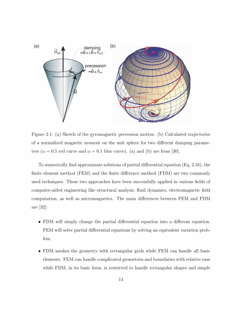
Figure 2.1: (a) Sketch of the gyromagnetic precession motion. (b) Calculated trajectories
of a normalized magnetic moment on the unit sphere for two different damping parame-
ters (α = 0.5 red curve and α = 0.1 blue curve). (a) and (b) are from [30].
To numerically find approximate solutions of partial differential equation (Eq. 2.16), the
finite element method (FEM) and the finite difference method (FDM) are two commonly
used techniques. These two approaches have been successfully applied in various fields of
computer-aided engineering like structural analysis, fluid dynamics, electromagnetic field
computation, as well as micromagnetics. The main differences between FEM and FDM
are [32]:
• FDM will simply change the partial differential equation into a different equation.
FEM will solve partial differential equations by solving an equivalent variation prob-
lem.
• FDM meshes the geometry with rectangular grids while FEM can handle all basic
elements. FEM can handle complicated geometries and boundaries with relative ease
while FDM, in its basic form, is restricted to handle rectangular shapes and simple
14
alterations.
• FDM can be easier implemented.
• The quality of a FEM approximation is often higher than in corresponding FDM
approach but quality of a simulation is extremely problem-dependent.
2.5 Micromagnetic Simulators
A micromagnetic simulator is a computer program carrying out micromagnetic simulations.
Micromagnetic simulators provide great freedom in the choice of experimental conditions
and material parameters, such as object geometry, initial magnetization, time evolution of
the external magnetic field, anisotropy, demagnetization factors, and the exchange inter-
action.
There are various commercial and free software packages available for micromagnetic
modeling and simulations. There are some highly successful packages such as OOMMF,
Magpar and LLG.
OOMMF, the Object-Oriented Micromagnetic Framework, is a free micromagnetic sim-
ulation tool using finite difference lattice discretisations of space and fast fourier transfor-
mation (FFT). It is a project of the Mathematical and Computational Sciences Division
of Information Technology Laboratory (ITL) at National Institute of Standards and Tech-
nology (NIST), developed mainly by Mike Donahue and Don Porter, and distributed freely
on the internet. It works user-friendly on a wide range of platforms.
Magpar is also an open source software package. It uses the finite element method for
calculation that gives large flexibility in modelling arbitrary geometries.
LLG micromagnetic simulator was developed in 1997 by Michael R. Scheinfein. It is a
widely used commercial software package using FDM.
15
Due to the uncertainty in the material parameters, the inaccurate experimental ge-
ometry, and the lack of material inhomogeneities, it is not reasonable to reproduce the
experimental curve quantitatively or reproduce the actual domain structure exactly [33].
I would like to focus on the experimentally observed results in a qualitative way, indepen-
dent of the exact simulation parameters [33]. By comparing imaging results and simulation
results, people gain a lot of understanding on magnetic properties of some applications on
sub-micron length scale.
2.6 Micromagnetic Systems
2.6.1 Hysteresis Loops
In a magnetic system, the plot of magnetization M versus magnetic field H is called the
M-H hysteresis loop. Here, we use M/MS instead of M which has values of 1 or −1 at
saturations. The ferro- and ferrimagnets show an interesting behaviour when the magnetic
field is reduced to zero and is reversed. A schematic plot of generic hysteresis loop is shown
in Fig. 2.2. It starts at the origin in an unmagnetized state, and then the curve goes to
saturation as an applied external positive magnetic field gradually increases. Then let the
magnetic field H reduce to zero from saturation, while the magnetization value M/MS
correspondingly decreases from saturation to the remanent magnetization MR/MS. A
reversed field which is required to reduce magnetization to zero is called coercive field, Hc.
Depending on the value of the coercive field, the ferromagnetic material can be classified as
either hard or soft [25]. When the external magnetic field continues decreasing, saturation
will be achieved in the reversed direction.
16
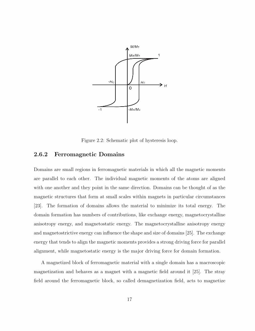
Figure 2.2: Schematic plot of hysteresis loop.
2.6.2 Ferromagnetic Domains
Domains are small regions in ferromagnetic materials in which all the magnetic moments
are parallel to each other. The individual magnetic moments of the atoms are aligned
with one another and they point in the same direction. Domains can be thought of as the
magnetic structures that form at small scales within magnets in particular circumstances
[23]. The formation of domains allows the material to minimize its total energy. The
domain formation has numbers of contributions, like exchange energy, magnetocrystalline
anisotropy energy, and magnetostatic energy. The magnetocrystalline anisotropy energy
and magnetostrictive energy can influence the shape and size of domains [25]. The exchange
energy that tends to align the magnetic moments provides a strong driving force for parallel
alignment, while magnetostatic energy is the major driving force for domain formation.
A magnetized block of ferromagnetic material with a single domain has a macroscopic
magnetization and behaves as a magnet with a magnetic field around it [25]. The stray
field around the ferromagnetic block, so called demagnetization field, acts to magnetize
17
the block in opposite direction from its own magnetization. Domain formation will reduce
the external demagnetization field which causes reducing magnetostatic energy. At the
same time, more magnetic moments are not able to align parallel, so the exchange energy
increases with domain formation. The battle between exchange energy and magnetostatic
energy determines domain formation.
Magnetocrystalline and magnetostrictive energies influence the shape and size of do-
mains. In ferromagnetic crystals, the magnetization tends to align along certain preferred
crystalline directions, so called easy axis. It is easiest to magnetize the demagnetized fer-
romagnetic block if the external magnetic field is applied along the easy axis. This causes
the magnetization to align itself along a preferred crystallographic direction. To minimize
the magnetocrystalline energy, the magnetization should point along the easy axis. Magne-
tocrystalline energy clearly affects the structures of the domain boundaries. At the region
between two adjacent domains, the magnetic moments cannot align along the easy axis,
so, like exchange energy, the magnetocrystalline energy prefers large domains [25]. When
a ferromagnet material is magnetized, it experiences a change in length, which is known as
its magnetostriction. Nickel is a material that shrinks along the direction of magnetization
and is said to have a negative magnetostriction. The length change is only tens of parts per
million but still affects the domain structure. The magnetostriction energy can be lowered
by reducing the size of the primary domains.
18
Chapter 3
Micromagnetic Investigation of the
S-State Reconfigurable Logic
Element
This chapter first introduces the S-state reconfigurable logic element. To establish a stable
geometrical stability criteria, a detailed analysis of the geometrical dimensions and shape
of the S-state logic element using micromagnetic simulations is performed. A general
introduction to the simulation setup and the discussion of figures-of-merit is given. First,
the dimensions of a rectangular element that suppress the formation of the undesired vortex
state are discussed; then we optimize the dimensions of the added appendages; and lastly
the influence of imperfections on the device characteristics are discussed. In the end, a
range of optimal geometrical parameters is presented.
19
3.1 S-State Reconfigurable Logic Element
Ferromagnetic nanostructures are attractive components of room-temperature magnetic
memory devices, logic devices [34, 35, 36, 6, 37], memory device and logic device combi-
nations [38, 39], as well as their combinations with CMOS [40]. In the 1950s and 60s [41],
magnetic logic devices were developed and they’re experiencing a comeback mainly due to
their non-volatility and comparably low-power consumption [42] in combination with the
ability to perform logic, storage, and amplification in a single device [5].
The magnetic logic devices require stable magnetization state that can be switched in
a binary fashion. The switching event can be inverting the rotation of a vortex state or
switching the direction of a magnetization into the opposite direction. A large number
of geometrical structures and materials are feasible, of which many have been explored
both numerically and experimentally, like disks, symmetric and asymmetric rings, ellipses,
triangles, trangle rings, Reuleaux triangles, and hexagons [43]. The concept of several
sub-elements magnetistatic coupling into logic gate [44, 7, 6] is very promising. However,
only a small number of these geological structures are turned out to be able to yield the
desired operation [45]. Structures with shapes different from rectangular and ellipse lead
to a more robust operation that is more tolerant to lithographic errors.
In Pampuch’s paper [46], the dominant magnetization direction in manganese arsenide
thin film can be switched as a function of two perpendicular magnetic input fields. A gen-
eralized concept of making use of common soft magnetic material Permalloy were presented
in [47]. An S-state is a common magnetization state that can be found in Permalloy prisms
in which magnetic moments assemble an ”S” liked state. Structures and materials were
discussed in our previous work [47] to support stable and useful S-state domain structures,
and the S shaped Permalloy element with perpendicular magnetic fields were demonstrated
the reconfigurable logic operation. It will also be shown in the following section.
20
S-state elements are potential magnetic random access memory (MRAM) [48]. Magne-
toresistive memory is based on a magnetic film being in one of two possible magnetization
states that can be switched by either applying perpendicular external magnetic fields [49] or
spin torque transfer (STT) [50]. The read-out can be achieved in the magnetoresistive stack
employing the GMR (giant magnetoresistance) [51] or TMR (tunnel magnetoresistance)
effect [52]. MRAM has advantages like nonvolatility, endurance, and hight speed [53], but
it also faces serious scaling challenges. The nanoscale magnetic elements have to be ther-
mally robust, yet the switching fields has to be within practical limits. Other challenges are
related to variations from element-to-element [54] and cycle to cycle [55]. S-state element
could be a good candidate due to its robust and shape-stabilized magnetization state.
In rectangular and elliptical nanostructures, S state magnetization pattern and C state
magnetization pattern are well known metastable states. The elongated nanostructures
contain quasi single domain states that has abrupt switching behaviour and gives squarelike
hysteresis loop. The C state can be generated by simply driving out a vortex state in the
elongated structures, while the S state can be left by reducing the perpendicular field after
the element reaching saturation magnetization.
The S-shaped magnetic logic element is presented in the work by Professor Hesjedal
[47]. To utilize the interesting S state in a device, the control over the device is needed.
Figure 3.1 shows the basic geometry of S-state element, two appendages are attached to
the rectangular center body.
The remanent state of the S-state element of suitable dimensions, specially dimensions
that suppress the formation of a vortex state, are shown in Fig. 3.2(a). The color scale
corresponds to the value of the x-component of the magnetization (blue → Mx/Ms = 0;
red → Mx/Ms = +1). The ideal (square-like), easy-axis hysteresis loops M∗x/M
∗s , are
shown in Fig. 3.2(b). The dashed line in this figure represents the unbiased curve. The
curve shifts to the left for a negative applied external magnetic field in the y-direction.
21
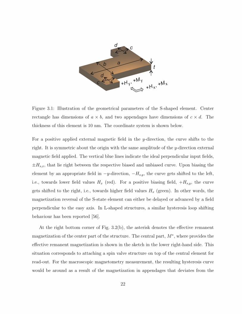
Figure 3.1: Illustration of the geometrical parameters of the S-shaped element. Center
rectangle has dimensions of a × b, and two appendages have dimensions of c × d. The
thickness of this element is 10 nm. The coordinate system is shown below.
For a positive applied external magnetic field in the y-direction, the curve shifts to the
right. It is symmetric about the origin with the same amplitude of the y-direction external
magnetic field applied. The vertical blue lines indicate the ideal perpendicular input fields,
±Hs,x, that lie right between the respective biased and unbiased curve. Upon biasing the
element by an appropriate field in −y-direction, −Hs,y, the curve gets shifted to the left,
i.e., towards lower field values Hx (red). For a positive biasing field, +Hs,y, the curve
gets shifted to the right, i.e., towards higher field values Hx (green). In other words, the
magnetization reversal of the S-state element can either be delayed or advanced by a field
perpendicular to the easy axis. In L-shaped structures, a similar hysteresis loop shifting
behaviour has been reported [56].
At the right bottom corner of Fig. 3.2(b), the asterisk denotes the effective remanent
magnetization of the center part of the structure. The central part, M∗, where provides the
effective remanent magnetization is shown in the sketch in the lower right-hand side. This
situation corresponds to attaching a spin valve structure on top of the central element for
read-out. For the macroscopic magnetometry measurement, the resulting hysteresis curve
would be around as a result of the magnetization in appendages that deviates from the
22
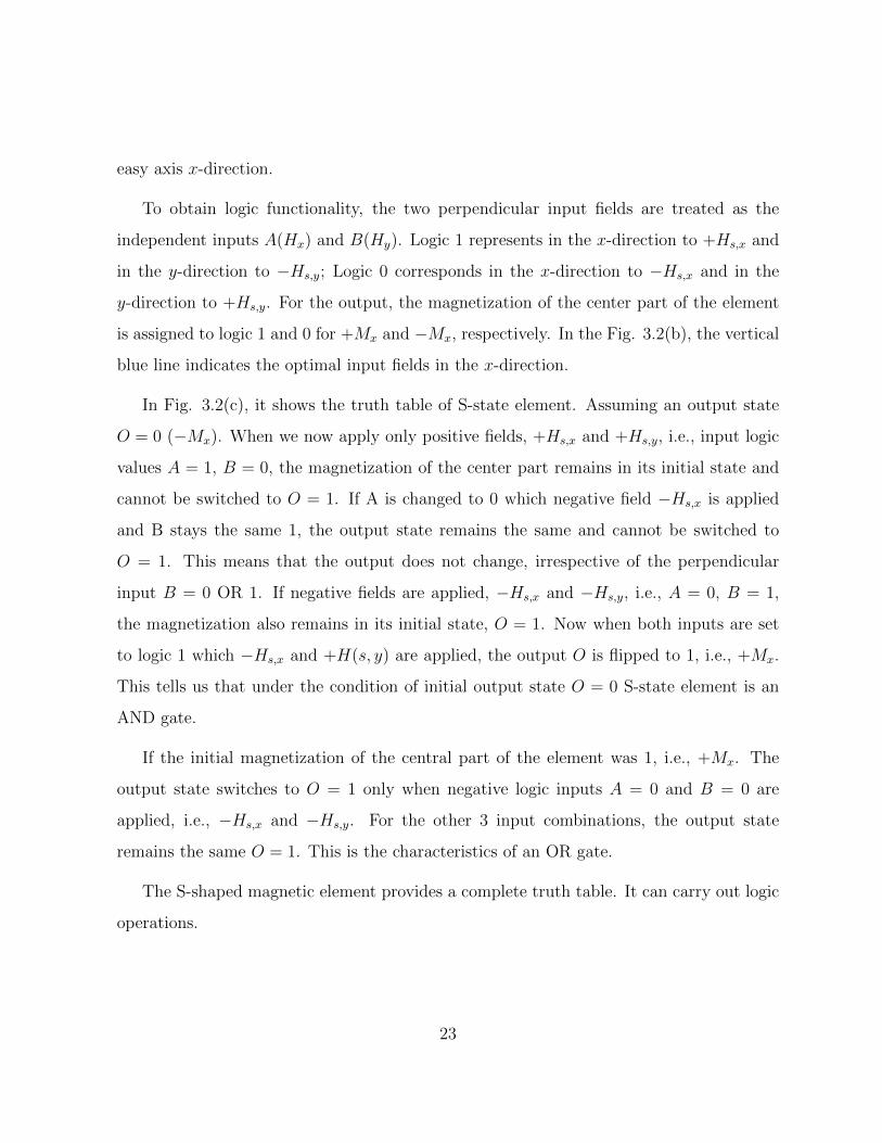
easy axis x-direction.
To obtain logic functionality, the two perpendicular input fields are treated as the
independent inputs A(Hx) and B(Hy). Logic 1 represents in the x-direction to +Hs,x and
in the y-direction to −Hs,y; Logic 0 corresponds in the x-direction to −Hs,x and in the
y-direction to +Hs,y. For the output, the magnetization of the center part of the element
is assigned to logic 1 and 0 for +Mx and −Mx, respectively. In the Fig. 3.2(b), the vertical
blue line indicates the optimal input fields in the x-direction.
In Fig. 3.2(c), it shows the truth table of S-state element. Assuming an output state
O = 0 (−Mx). When we now apply only positive fields, +Hs,x and +Hs,y, i.e., input logic
values A = 1, B = 0, the magnetization of the center part remains in its initial state and
cannot be switched to O = 1. If A is changed to 0 which negative field −Hs,x is applied
and B stays the same 1, the output state remains the same and cannot be switched to
O = 1. This means that the output does not change, irrespective of the perpendicular
input B = 0 OR 1. If negative fields are applied, −Hs,x and −Hs,y, i.e., A = 0, B = 1,
the magnetization also remains in its initial state, O = 1. Now when both inputs are set
to logic 1 which −Hs,x and +H(s, y) are applied, the output O is flipped to 1, i.e., +Mx.
This tells us that under the condition of initial output state O = 0 S-state element is an
AND gate.
If the initial magnetization of the central part of the element was 1, i.e., +Mx. The
output state switches to O = 1 only when negative logic inputs A = 0 and B = 0 are
applied, i.e., −Hs,x and −Hs,y. For the other 3 input combinations, the output state
remains the same O = 1. This is the characteristics of an OR gate.
The S-shaped magnetic element provides a complete truth table. It can carry out logic
operations.
23
Figure 3.2: (a) Remanent magnetization distribution in a Permalloy S-shaped element. (b)
Idealized hysteresis curve of a biased S-shaped element. (c) Logic table for the S-shaped
element.
24
3.2 Simulation Setup
The geometric parameters of S-shaped element play an important role in stabilizing the
logic functionality. The goal of the work in this section is to establish geometrical stability
criteria for S-shaped logic elements. We start with the simplest, symmetric structures
which will lay the foundation for more complex, independent input variations in the future.
The basic structure consists of a rectangular center part with dimension a × b and two
appendages symmetrically attached to the center body with dimension c× d, as shown in
Fig. 3.1. Two appendages will be able to vary in shape and area, and respond to input
field in the y-direction will be different. Asymmetric appendages add additional degree of
design freedom.
The micromagnetic simulations were performed using Scheinfein’s LLG simulator [57].
For the investigation of the Permalloy structures, the following micromagnetic constants
were used: a saturation magnetization of Ms = 800 emu/cm3, an exchange constant of
A = 1.05 × 10⁻⁶ erg/cm3, and a uniaxial anisotropy constant of K = 1000 erg/cm3. The
simulations were carried out on a Cartesian grid with ∆x = ∆y = ∆z = 5 nm at 0 K.
To utilize the the S-state element, it has to be integrated into a suitable device structure.
The most simple realization comprises address lines providing perpendicular Oersted fields
for the inputs, and a magnetoresistive readout structure. Hereby the S-state element will
be the free layer in a magnetoresistive trilayer structure, such as a giant-magnetoresistance
(GMR) [51] or spin-dependent tunnelling (TMR=tunnel magnetoresistance) [52] device.
To optimize the read-out signal, the magnetization in the section of the S-state element
that is part of the magnetoresistive element should be fully in the x-axis direcrion. For
exploring the usable geometrical parameter space, the following general criteria have to be
taken into consideration:
• In magnetoresistive trilayer structures, the projection of the free layer can be effec-
25
tively read out. For optimizing the read-out signal, the projected magnetization of
the central part of the S-state element has to be fully aligned with the fixed layers
in the magnetoresistive stack. Thus, the hysteresis loops should be square-like, i.e.,
Mr/Ms should be close to unity and the roundedness of the shoulders should be
small. This limits the relative size of the appendages over the center rectangle which
should not be too large which causes value reduction of Mr/Ms.
• The first criterion implies that the magnetization state in the center rectangle is quasi
single-domain. This requires the rectangle to be below a certain size, and to have a
rather elongated shape, in order to avoid the formation of a vortex state.
• The functionality of the S-shaped element depends on a sufficiently large shift of the
hysteresis due to the biasing field ±Hy. The sufficient large shift results in a more
reliable operation and less stringent fabrication requirements, so that small shifts of
the coercive field due to structural imperfections, such as rounded edges and sidewall
roughness, can be tolerated.
• Ideally, the coercive fields applied to the x- and y-directions should be of the same
magnitude, or, to be more precise, the driving fields used to switch the elements
should be as symmetric as possible. This adds another criterion to the relative size
of the appendages over the center rectangle.
• The coercive field has to be chosen in a proper range. If Hc is too large, the switch-
ing process will require too much energy so this device is expensive from perspective
of the energy cost. If Hc is too small, the element will be unstable due to rela-
tively large magnetic field noise or relatively large imperfection caused by fabrication
imperfection.
26
3.3 Remanent Magnetization Patterns in Rectangu-
lar Prisms
To systematically study parameter space of the S-state element, first, we investigate the
parameters of the center rectangle. As we mentioned before we have the center rectangle
with dimension a × b. To integrate the S-state into a standard magnetoresistive layer
structure requires the magnetization in the center rectangle that overlap with the magnetic
sensor stack to be quasi single-domain. Besides, to prevent the demagnetization due to
thermal fluctuations, single-domain state in the center rectangle is also desirable.
The remanent state of rectangular Permalloy prisms have dependence of the thickness
and size [58]. In specific geometry, quasi-homogeneous sigle-domain states and demagne-
tized flux-closure patterns can exist in the length range between 250 and 1000 nm. In
Permalloy rectangles, common quasi single domain patterns are S-state and the C-state.
Common flux-closure patterns are the Landau state (one vortex) and the diamond state
(two vortices). Stray field energy which favours flux-closure patterns and exchange energy
which favours homogeneous magnetization compete with each other. The competition
between stray field energy and the exchange energy determines if flux-closure patterns ex-
hibit. In general, as structure size becomes smaller, the exchange energy becomes more
significant than the stray field energy, and the stray field-reducing flux-closure patterns are
less common due to their relatively high exchange energy.
In the most general cases, lateral dimensions, thickness, and magnetic material proper-
ties determine the details of the phase diagram of remanent magnetization patterns. In our
analysis, thin Permalloy films which are commonly used in practical device applications
were used. The magnetization pattern in soft magnetic Permalloy is largely dependant on
the shape anisotropy which determines the stray field energy distribution [23]. Theoret-
ically, the thickness of thin film doesn’t affect the energy density of a thin film element
27
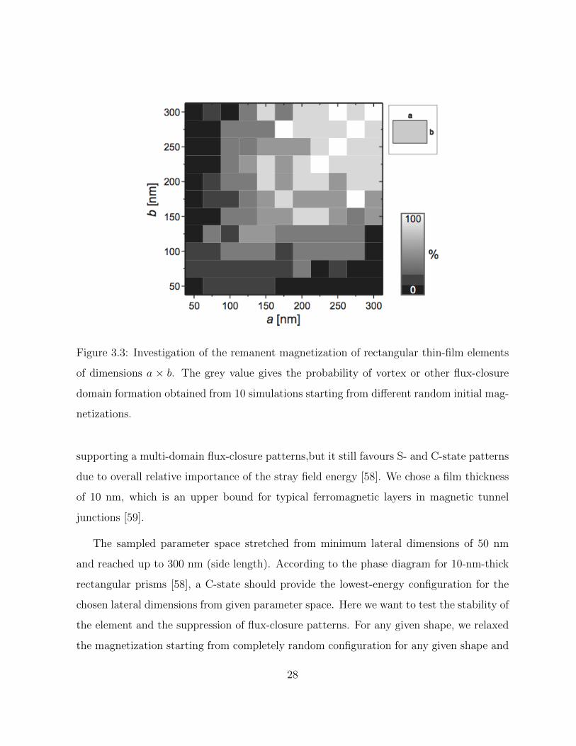
Figure 3.3: Investigation of the remanent magnetization of rectangular thin-film elements
of dimensions a × b. The grey value gives the probability of vortex or other flux-closure
domain formation obtained from 10 simulations starting from different random initial mag-
netizations.
supporting a multi-domain flux-closure patterns,but it still favours S- and C-state patterns
due to overall relative importance of the stray field energy [58]. We chose a film thickness
of 10 nm, which is an upper bound for typical ferromagnetic layers in magnetic tunnel
junctions [59].
The sampled parameter space stretched from minimum lateral dimensions of 50 nm
and reached up to 300 nm (side length). According to the phase diagram for 10-nm-thick
rectangular prisms [58], a C-state should provide the lowest-energy configuration for the
chosen lateral dimensions from given parameter space. Here we want to test the stability of
the element and the suppression of flux-closure patterns. For any given shape, we relaxed
the magnetization starting from completely random configuration for any given shape and
28
repeated for ten times. The times that forms a flux-closure pattern were counted and the
results of the simulations were plotted as a function of length, a, and width, b, in Fig. 3.3.
The grey values indicate the likelihood of finding a flux-closure pattern in the rectangle
prisms. From the Fig. 3.3, we can tell that the probability of vortex formation increases
as the area increases, and is higher for more square-like structures (a ≈ b). Away from the
square-like structures, we can tell that elongated structures suppress the vortex formation.
As the lateral dimension extends, the grey value increases so there will be a upper limit for
the lengths. At a thickness of 10 nm, useful rectangular prisms should have a maximum
dimension of the smaller length of ∼ 125 nm.
In order to stabilize the S-state or C-state, and to increase the usable parameter range,
we can biasing the center rectangular prism with adjacent magnetic elements to force
the formation of S-state or C-state, e.g., used in magnetic logic arrays [6]. The adjacent
elements make magnetostatic dipole coupling with center rectangle. Instead of adding
adjacent elements, add magnetic material at selected locations. This method can stabilize
the preferred states as well and avoid the fabrication challenges associated with narrow
gaps. Here we chose S-state pattern over C-state pattern. Generally the S-state pattern
has an advantage over C-state pattern. For S-state pattern, the magnetization direction of
the added elements (appendages) is pointing in the same direction, which allows to apply
an external field globally instead of locally to each appendage. But if local magnetization
reversal techniques such as spin torque transfer are employed, the C-state element gives a
larger versatility.
Figure 3.1 shows the general layout of S-state element. The appendage size should
neither be too small as a sufficient biasing effect need to be achieved, nor too large as this
would lead to a reduced project along the x-direction or deform the magnetization pattern
in the center of the structure. A reasonable compromise is using 40× 50 nm2. The S-state
elements with variable center rectangle size and fixed appendage size, 40× 50 nm2.
29
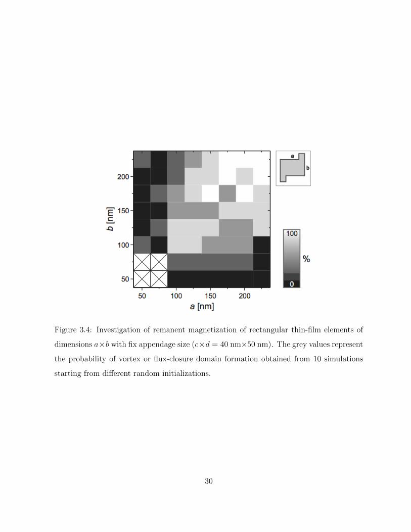
Figure 3.4: Investigation of remanent magnetization of rectangular thin-film elements of
dimensions a×b with fix appendage size (c×d = 40 nm×50 nm). The grey values represent
the probability of vortex or flux-closure domain formation obtained from 10 simulations
starting from different random initializations.
30
To test the stability of S-shaped element and the suppression of flux-closure patterns, we
relaxed the magnetization starting from the completely random configuration and repeated
the simulation ten times. The result of simulation is plotted as a function of center rectangle
prism lateral dimensions a, the length, and b, the width, as shown in Fig. 3.4. Also, the grey
values indicate the likelihood of forming a flux-closure pattern. Compared with the case
without appendages (Fig. 3.3), the structure becomes more unstable from the perspective
of flux-closure domain formation. Also, even the smaller square-like structures will more
likely develop vortex patterns. This is an important detail that we need to bear in mind, as
it is counterintuitive that the presence of appendages increases the probability of forming
vortex states. Nevertheless, the addition of the appendages is essential for optimizing the
effectiveness of the perpendicular in-plane field.
After analysing Figure 3.3 and Figure 3.4, additional restrictions on the center rectan-
gular prism parameter space are added. Naturally, as the structure gets longer, a lesser
tendency towards vortex formation is observed. In this section, we used completely ran-
dom magnetization as initial input, while, during operation of the device, the element is
never coming out of a completely random magnetization state. As a result, the element
will be much more stable against spontaneous vortex formation. If, for example, a useful
minimum feature size of 100 nm is assumed for the rectangle, the longer side should be at
least 150 nm long. The aspect ratio of the rectangle should thus at least 1.5:1.
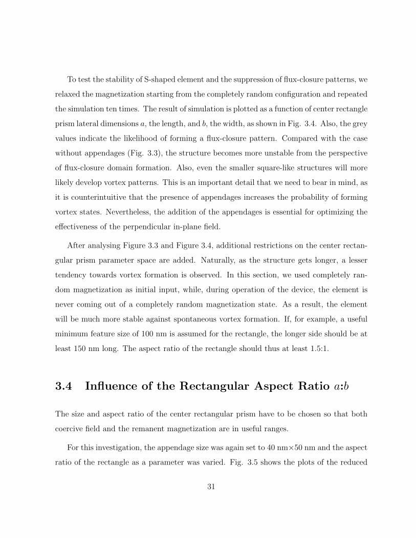
3.4 Influence of the Rectangular Aspect Ratio a:b
The size and aspect ratio of the center rectangular prism have to be chosen so that both
coercive field and the remanent magnetization are in useful ranges.
For this investigation, the appendage size was again set to 40 nm×50 nm and the aspect
ratio of the rectangle as a parameter was varied. Fig. 3.5 shows the plots of the reduced
31
Figure 3.5: Plot of coercive field, Hc, and reduced remanent magnetization, Mr/Ms, of
S-state elements as a function of length of the center rectangle, a. The rectangle width is
fixed at b = 100 nm and the appendages are measuring 40 nm×50 nm.
32
remanent magnetization, Mr/Ms, and the coercive field, Hc, as a function of a/b for a fixed
width of b = 100 nm, obtained from the hysteresis loops. In this plot, the reduced remanent
magnetization is measured an area of 100× 100 nm2 in the center of the rectangle, which
is the assumed size of the magnetoresistive sensor element, shown as area of M∗ in Fig.
3.2(b).
As a high reduced remanent magnetization of close to unity is desirable for large read-
out signals of the magnetoresistive sensor, an aspect ratio of at least 1.4 has to be chosen.
Above the requirement of high reduced remanent, however, the coercive field is already
approaching 300 Oe, while the smaller fields of ∼150 Oe as shown in the plots would
certainly be better in terms of power requirements.
3.5 Study of the Appendage Size
In this section we optimized the appendages in terms of overall area and aspect ratio.
To investigate the influence of ear size, we kept the center rectangle fixed at a × b =
150× 100 nm2. Figure 3.6 shows the plot of remanent magnetization (a) and the coercive
field (b) of S-state elements as a function of the aspect ratio c/d of the appendages and
for five different appendage areas ranging from c× d = 1000 to 3000 nm2.
When the aspect ration c/d increases for the given appendage area c× d, Mr/Ms and
Hc generally decrease. For a fixed aspect ratio, Mr/Ms and Hc also decrease as the area
increases. When the appendage aspect ratio c/d is between 0.2 to 1.25, the coercive field
values remain rather similar at a value between 300 and 500 Oe. The reduced remanent
magnetization stays above 90%, except for large appendages (2500 and 3000 nm2) If the
aspect ratio is further increased beyond 1.25, the coercive field decreases dramatically,
which means that there is not enough effective biasing due to the appendages. The reduced
remanent magnetization follows the same trend, however, the slope is not as steep for
33
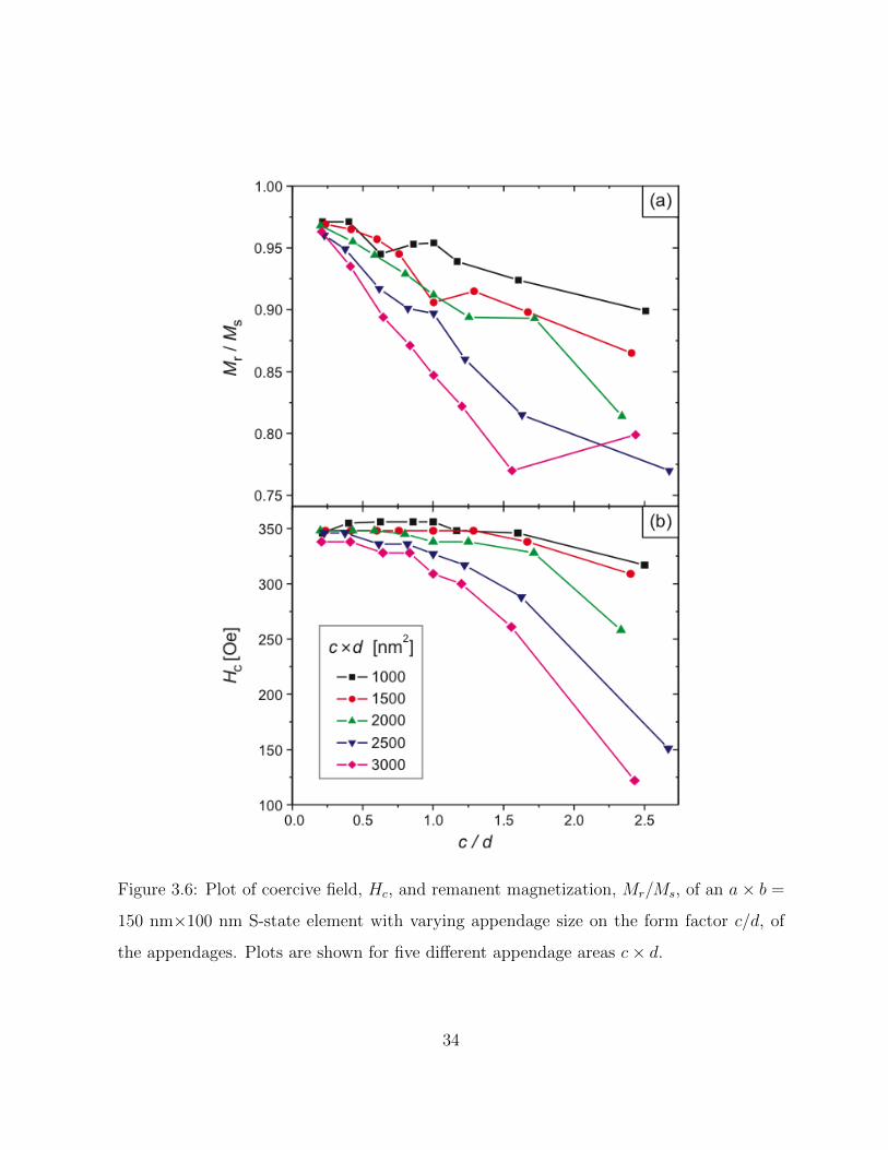
Figure 3.6: Plot of coercive field, Hc, and remanent magnetization, Mr/Ms, of an a× b =
150 nm×100 nm S-state element with varying appendage size on the form factor c/d, of
the appendages. Plots are shown for five different appendage areas c× d.
34
smaller appendages. decreases with a less steep slope than coercive field.
In summary, appendages with areas of 1000 to 2000 nm2 stabilize the S-state in the
center of the structure well for aspect ratios of up to c/d = 5/3, while the reduced remanent
magnetization stays above 90%.
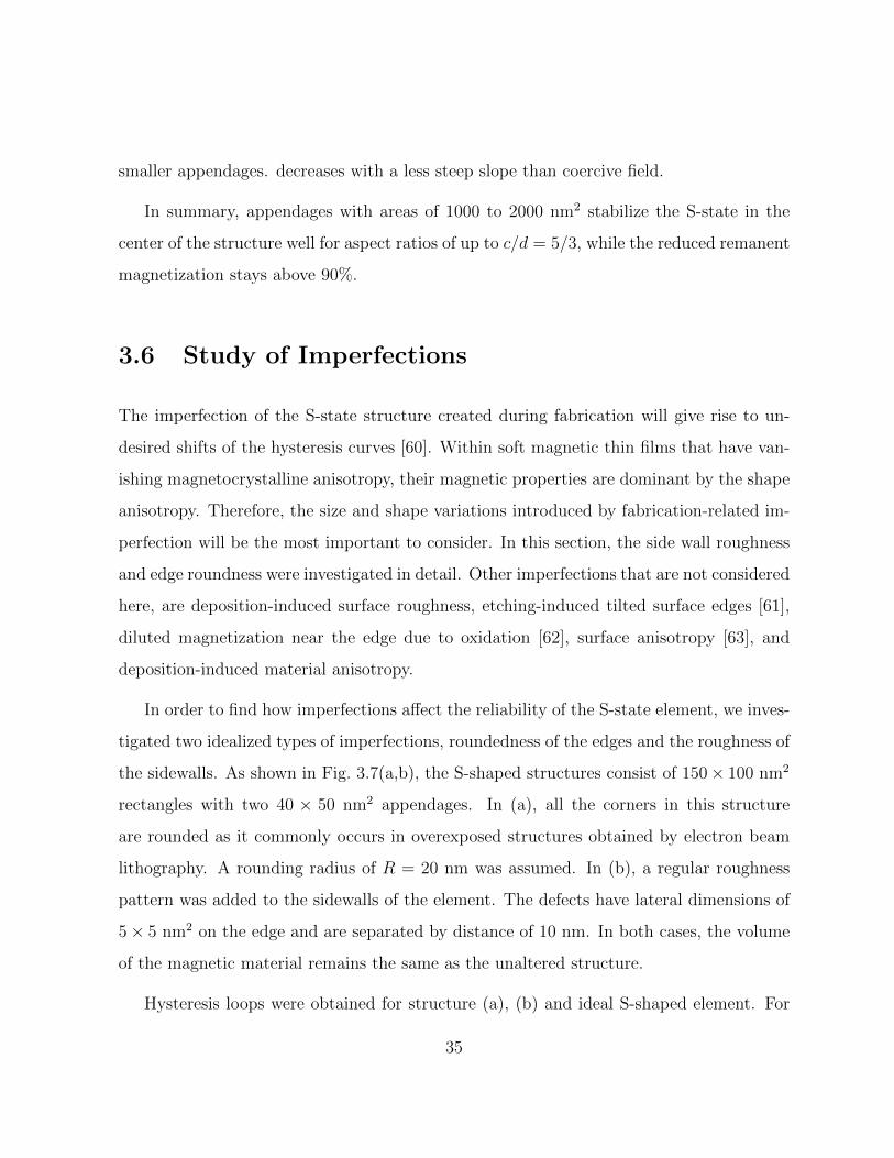
3.6 Study of Imperfections
The imperfection of the S-state structure created during fabrication will give rise to un-
desired shifts of the hysteresis curves [60]. Within soft magnetic thin films that have van-
ishing magnetocrystalline anisotropy, their magnetic properties are dominant by the shape
anisotropy. Therefore, the size and shape variations introduced by fabrication-related im-
perfection will be the most important to consider. In this section, the side wall roughness
and edge roundness were investigated in detail. Other imperfections that are not considered
here, are deposition-induced surface roughness, etching-induced tilted surface edges [61],
diluted magnetization near the edge due to oxidation [62], surface anisotropy [63], and
deposition-induced material anisotropy.
In order to find how imperfections affect the reliability of the S-state element, we inves-
tigated two idealized types of imperfections, roundedness of the edges and the roughness of
the sidewalls. As shown in Fig. 3.7(a,b), the S-shaped structures consist of 150× 100 nm2
rectangles with two 40 × 50 nm2 appendages. In (a), all the corners in this structure
are rounded as it commonly occurs in overexposed structures obtained by electron beam
lithography. A rounding radius of R = 20 nm was assumed. In (b), a regular roughness
pattern was added to the sidewalls of the element. The defects have lateral dimensions of
5× 5 nm2 on the edge and are separated by distance of 10 nm. In both cases, the volume
of the magnetic material remains the same as the unaltered structure.
Hysteresis loops were obtained for structure (a), (b) and ideal S-shaped element. For
35
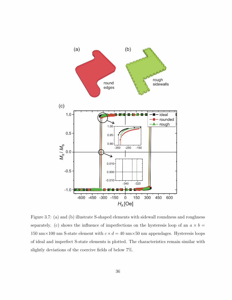
Figure 3.7: (a) and (b) illustrate S-shaped elements with sidewall roundness and roughness
separately. (c) shows the influence of imperfections on the hysteresis loop of an a × b =
150 nm×100 nm S-state element with c×d = 40 nm×50 nm appendages. Hysteresis loops
of ideal and imperfect S-state elements is plotted. The characteristics remain similar with
slightly deviations of the coercive fields of below 7%.
36
a ideal S-state element with perfect geometry structure, the coercive field is 348 Oe. The
coercive value reduces to 329 Oe for the element with rounded corners and to 302 Oe for
element with rough sidewalls. In (c), close-ups show the effect of the imperfections on
the roundedness of the hysteresis loop in greater detail. None of the considered imperfec-
tions alters the hysteresis curve for the selected element qualitatively. The two types of
imperfection give hysteresis loop shift up to 46 Oe. Bear the shift value 46 Oe in mind,
to guarantee the switching events during logic operation correctly occur, the hysteresis
loop shift created by biasing field has to be significantly larger than 46 Oe. We note that
the shift of the coercive field is sensitive to sidewall roughness especially when the vortex
motion is part of the reversal process.
Simulations of perfect and imperfect rectangles with length of 150 nm and width 100 nm
were carried out. For the rectangle with perfect structure, coercive field of 343 Oe was
obtained. The reversal proceeded via C-state formation which lead to the roundedness of
its hysteresis curve, and switched abruptly at coercive field via the creation, propagation,
and annihilation of a vortex state. The reversal process with formation of S-state is quite
similar to the reversal process with formation of C-state, except that it has slightly higher
coercive field 347 Oe. In contrast to this behaviour, rough rectangle tended to pin the initial
C-state. The hysteresis loop shows that, after the initial roundness, a linear decrease that
persists even down to negative values of the magnetization, before the abrupt reversal
happens at a values of 443 Oe. Within reasonable limit, it is found that the detail of edge
roughness, i.e., magnitude and frequency of the defects, do not affect the principal reversal
process; and the coercive field values typically range from 347 Oe and 590 Oe. We can see
that the range of coercive field of simple rectangle is at least twice as large as in the case
of S-state element.
To obtain the trend of coercive field shift as a function of geometry and defects, a set of
simulations was carried out on selected S-state configurations. The results are summarized
37
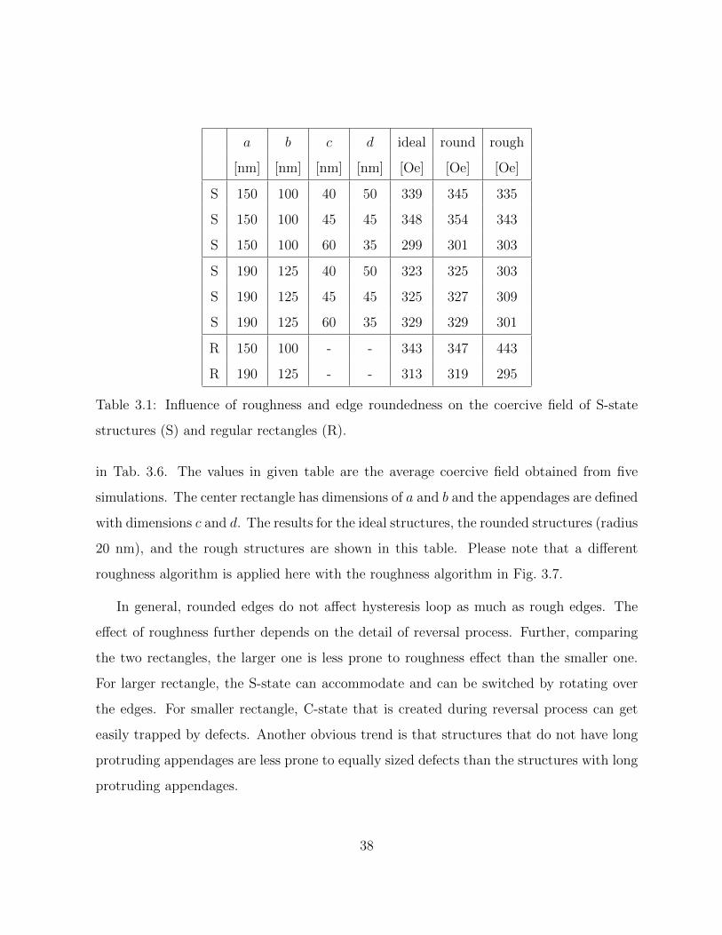
a b c d ideal round rough
[nm] [nm] [nm] [nm] [Oe] [Oe] [Oe]
S 150 100 40 50 339 345 335
S 150 100 45 45 348 354 343
S 150 100 60 35 299 301 303
S 190 125 40 50 323 325 303
S 190 125 45 45 325 327 309
S 190 125 60 35 329 329 301
R 150 100 - - 343 347 443
R 190 125 - - 313 319 295
Table 3.1: Influence of roughness and edge roundedness on the coercive field of S-state
structures (S) and regular rectangles (R).
in Tab. 3.6. The values in given table are the average coercive field obtained from five
simulations. The center rectangle has dimensions of a and b and the appendages are defined
with dimensions c and d. The results for the ideal structures, the rounded structures (radius
20 nm), and the rough structures are shown in this table. Please note that a different
roughness algorithm is applied here with the roughness algorithm in Fig. 3.7.
In general, rounded edges do not affect hysteresis loop as much as rough edges. The
effect of roughness further depends on the detail of reversal process. Further, comparing
the two rectangles, the larger one is less prone to roughness effect than the smaller one.
For larger rectangle, the S-state can accommodate and can be switched by rotating over
the edges. For smaller rectangle, C-state that is created during reversal process can get
easily trapped by defects. Another obvious trend is that structures that do not have long
protruding appendages are less prone to equally sized defects than the structures with long
protruding appendages.
38
3.7 Optimization of the Biasing Field
In this section, we will discuss the choice of the biasing field and the influence of the
geometrical parameters on its optimum value. The biasing field Hy is one of the inputs
required for the logic operation. It is perpendicular to the easy axis of the rectangular
center prism. As it is known from last section, geometric imperfections will lead to an
undesired shift of the hysteresis loops that compromises the function of the device. So,
the coercive field shift, the effect of the biasing field, has to be sufficiently larger than all
distortions combined.
To study the biasing field effect, different structural configuration were analysed. The
rectangular center structure has a fixed width of b = 100 nm and a variable length a leading
to aspect ratios of a/b = 1.25, 1.50, 1.75, and 2.00. For the two appendages, size 2000 nm2
was chosen with different form factors of c/d = 0.2 (20×100 nm2) to 2.33 (70×30 nm2) were
selected. The choice of parameters was governed by the results obtained and discussed in
the previous subsections.
Because of the biasing, every hysteresis loop has now two distinctly different coercive
field values. For simplicity, Hc always refers to the larger of the two values of the coercive
fields. The overall shift of the hysteresis loops is expressed by ∆Hc = |Hc(+Hy)−Hc(−Hy)|.
From the previous section, we obtained a coarse estimate of the imperfection-induced
coercive field shift of 48 Oe. As this shift occurs in both biasing directions, ∆Hc has to be
at least larger than 96 Oe which doubles 48 Oe. For convenience, 100 Oe contour line is
outlined in Fig. 3.8.
Figure 3.8 shows contour plots of the coercive field shift ∆Hc as a function of rectan-
gular aspect ratio, a/b, and appendage aspect ratio, c/d, for three different values of the
perpendicular biasing field Hy. The three plots correspond to a Hy of 50 Oe (a), 100 Oe
(b), and 150 Oe (c). In all three plots, the 100-Oe-limit contour defines acceptable geom-
39
Figure 3.8: Shift of the coercive field, ∆Hc, as a function of rectangle form factor, a/b, and
appendage form factor, c/d. The results for three different biasing fields, Hy, are shown:
(a) 50 Oe (b) 100 Oe, and (c) 150 Oe. All elements have the same body width b = 100 nm
and appendage area c× d ≈ 2000 nm2. Dash lines indicate the 100-Oe-limit.
40
etry areas. The unusable areas are where the shift is less than 100 Oe. In general, the
coercive field shift ∆Hc increases with the value of a/b, while its c/d dependence shows
more pronounced maxima and minima. For Hy = 50 Oe (a), acceptable aspect ratios are
linearly increasing with the a/b ratio. For a/b = 1.2, the c/d has to be chosen under 0.4
while for a/b > 1.75 the entire tested c/d range is usable. For Hy = 100 Oe, Hc is by
choice always larger than Hy. Hc differences remains small. For Hy = 150, acceptable
aspect ratios are confined to an area below a line reaching from c/d = 0.8 at a/b = 1.2 to
c/d = 2.5 at a/b = 1.5. Remarkably, large shifts ∆Hc are found for c/d ∈ [0.4, 0.6] and
a/b > 1.45.
Another design criterion for S-shaped logic element is that biasing field and coercive
field should have roughly the same magnitude. If the rectangular aspect ratio is chosen to
be greater than 1.4, the coercive field Hc (without biasing field) is roughly between 300 and
550 Oe (cf. Subsec. 3.5). After adding the biasing field Hy, the (larger) coercive field value
|Hc + ∆Hc| will be in the interval [300 + ∆Hc, 550 + ∆Hc]. If, for instance, ∆ > 450 Oe
the coercive field can become greater than 1000 Oe, which by itself is a large value and
also much larger than the other input field value. Since ∆Hc generally increases with a/b,
the upper limit of acceptable ∆Hc values will also give an upper boundary for the aspect
ratio a/b.
For the appendages, the areas in which the coercive field shift ∆Hc is larger than 100 Oe
is somewhat more complex. When the aspect ratio c/d of the appendages is too large, they
will effectively become a part of the rectangular prism and simply increase its width b by
(2 · c) - without having a biasing effect on the central structure. If c : d is too small, the
appendages become too small to sufficiently alter the magnetization pattern of the center
structure. The upper and lower bounds for c : d are clearly visible in Figure 3.8(b,c),
whereas the upper cut-off in (a) is beyond the simulated parameter range. Also note that
the contact area between appendages and rectangular prism, c, is limited by the choice of
41
discretization length, which is 5 nm for the present simulations. A length of 5 nm agrees
well with exchange length in Permalloy of 5.3 nm.
3.8 Discussion
The commonly known S-state magnetization pattern in soft magnetic thin film elements
is an interesting feature. It can be exploited for magnetic logic operations. The working
principle of S-shaped element is the shift of the hysteresis loop of the rectangle due to the
applied perpendicular in-plane fields which is along the width of the center rectangle. Two
inputs are provided to address the element and obtain logic operation.
In rectangular Permalloy prisms with a thickness of t = 10 nm, the S-state pattern is not
a minimum energy configuration. Two appendages were added to the center rectangle to
force the element into an S-state magnetization pattern as the lowest energy configuration.
So, as a first step, the rectangular prisms were chosen as to suppress the formation of vortex
and other closed-flux domain patterns. In general, it requires that the structure should be
(i) small, as the exchange energy becomes relatively more important in small structures
and disfavours domain formation, and (ii) elongated, as elongated rectangle prism leads
to the formation of a disfavoured magnetization direction thereby suppressing some, but
not all, flux-closure patterns. While stretching the rectangle increases value of coercive
field, which eventually affects the integration density due to the large required switching
fields. Although small center rectangle favours the desired S-state magnetization, the inner
area that is to become free layer in a magnetoresistive layer stack needs to match with the
commonly used, or anticipated, GMR or TMR sensor footprint. As a minimum feature
size of 100 nm has been common in TMR elements for some time now [64]. The same size
has been chosen for the width of the center rectangle in this investigation. As part of this
device integration it has been made sure that the magnetization in this area is fully aligned
42
with the long axis of the rectangle to maximize the read-out signal.
The appearance of the appendages certainly affects the magnetization pattern of the
rectangular prism. Obviously, very small, as well as very large, appendages will not stabilize
an S-state. In the case of very small appendage size, they would be simply too small to
make difference. In the other case which the appendages are comparably large, they could
be so big that they essentially become an integral part of an enlarged rectangle. A good
compromise is an appendage area of 1000-2000 nm2.
Two inputs are provided to address the element and obtain logic operation. The two
inputs can use the straight-forward way in which current-carrying wires proving sufficiently
large Oersted fields. As the fields have to be crossed, the two write lines would have to
be placed for example above and below the S-state element. Another way to apply the
two inputs is using spin torque transfer (STT) [50]. This includes not only the central
rectangle, which needs to contacted by a GMR or TMR sensor, but also the appendages.
This solution, although elegant, poses serious fabrication problems as three separate STT
structures would be needed that would have to be very close together. Further, as non-
collinearly magnetized reference layers are needed two separate fabrication process runs
for the STT-driven GMR or TMR stacks are needed.
Another noteworthy feature of S-state element is its relative reproducibility of switching
behaviour, and thus the coercive field values. Compared to S-state element, the simple
rectangle gives larger deviations on coercive field values in simulation. The reason why
added roundness and roughness defects do not affect S-state element to the same degree
with simple rectangle might lie in the fact that appendages can be seen as defects which
dominant the nature of the switching process. The edge defects have relatively less impact.
In fact, the magnetization reversal of S-state structures always proceeds via rotations of
the magnetization in the appendages, while magnetization reversal of simple rectangles
would strongly depends on the detail of defect structures. Therefore, it is conceivable that
43
S-state element might be employed in MRAM cells as they have potential to reduce the
element-to-element and cycle-to-cycle variations in the switching field.
3.9 Summary
In this chapter, I presented a detailed micromagnetic analysis of the useful geometrical
parameter space for S-state magnetic logic elements. An S-state element essentially relies
on the biasing effect of a perpendicular in-plane field on its hysteresis loop, which is a
shift of the coercive field. We defined several design criteria that are critical for the logic
operation. The size and aspect ratio of the center rectangular prism were chosen so that
flux-closure magnetization patterns are suppressed. A good choice is a maximum width
of the rectangle of 125 nm and a length that is at least ≈ 190 nm, using form factor of
1.5. In order to force the formation of an S-state pattern and maximize the effect of a
perpendicular biasing field on the magnetization characteristic, appendages were attached
to the rectangular prism. Each appendage should have an area between 1000 and 2000 nm2,
and an aspect ratio of up to 5/3. It is important to simultaneously attempt to maximize
the alignment of the magnetization of the central part of the rectangle along the easy
axis direction. The effect of biasing field was investigated together with a variation of the
geometrical parameters. At the biasing field between 150 Oe and 200 Oe, while keeping
the perpendicular field at the same range, the element with a large selection of geometrical
parameters will perform the logical operation.
44
Chapter 4
Self-assembly of Magnetic Nanowires
4.1 Introduction
Magnetic nanowires are highly attractive materials that have potential for applications in
ultrahigh magnetic recording, logic operation devices, and micromagnetics and spintronics
sensors. In order to fabricate these potential devices, one of the challenges is to find a way
to pattern these nanowires controllably and effectively. There are two basic approaches:
top-down and bottom-up. For the pre-synthesized nanostructures, bottom-up assembly is
the way to build nanodevices.
In this chapter, ferromagnetic nickel nanowires are synthesized by electrodeposition.
Ni nanowires with a diameter of 200 nm are terminated by Au end caps in order to al-
low for further etching. Magnetic alignment is a facile technique for assembling nanowires
into hierarchical structures [21]. It is an appealing approach which is capable of align-
ing thousands of nanowires in two dimensions. From the micromagnetic point of view,
one major question that needs to be addressed is how the nanowires respond to exter-
nal magnetic fields - either due to other nanowires in an ensemble or additionally added
magnetic fields. Here, we investigate the magnetic remanence and reversal properties in
45
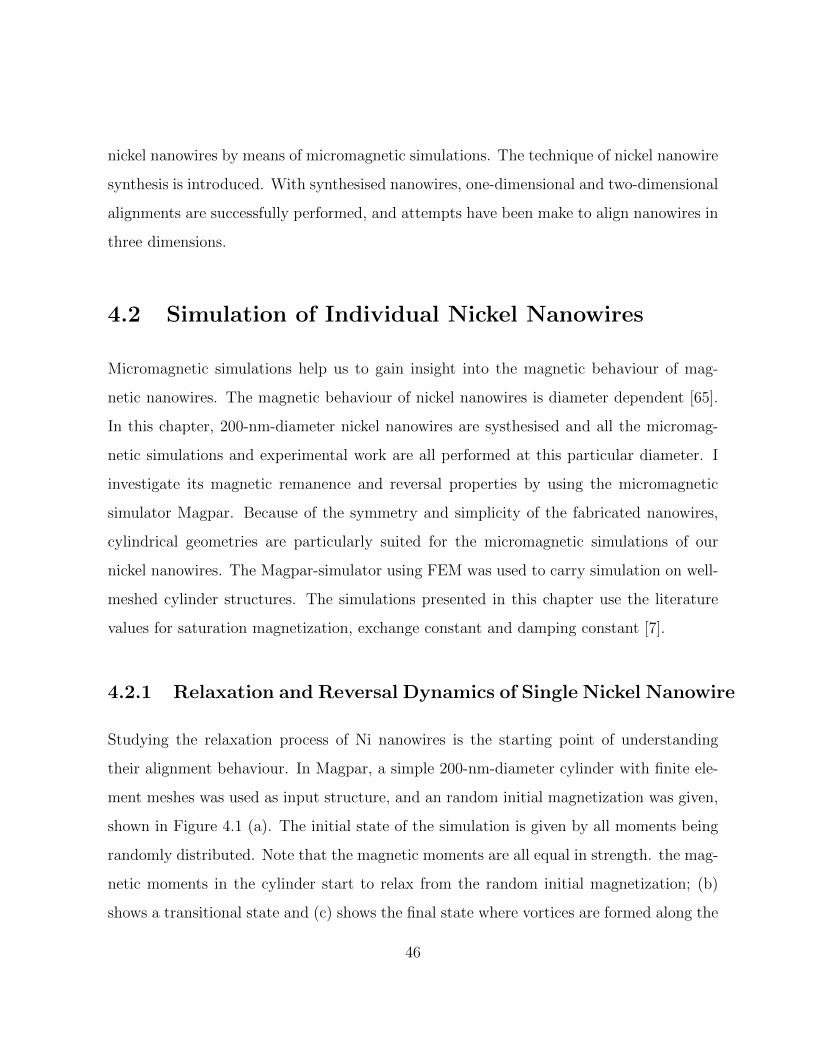
nickel nanowires by means of micromagnetic simulations. The technique of nickel nanowire
synthesis is introduced. With synthesised nanowires, one-dimensional and two-dimensional
alignments are successfully performed, and attempts have been make to align nanowires in
three dimensions.
4.2 Simulation of Individual Nickel Nanowires
Micromagnetic simulations help us to gain insight into the magnetic behaviour of mag-
netic nanowires. The magnetic behaviour of nickel nanowires is diameter dependent [65].
In this chapter, 200-nm-diameter nickel nanowires are systhesised and all the micromag-
netic simulations and experimental work are all performed at this particular diameter. I
investigate its magnetic remanence and reversal properties by using the micromagnetic
simulator Magpar. Because of the symmetry and simplicity of the fabricated nanowires,
cylindrical geometries are particularly suited for the micromagnetic simulations of our
nickel nanowires. The Magpar-simulator using FEM was used to carry simulation on well-
meshed cylinder structures. The simulations presented in this chapter use the literature
values for saturation magnetization, exchange constant and damping constant [7].
4.2.1 Relaxation and Reversal Dynamics of Single Nickel Nanowire
Studying the relaxation process of Ni nanowires is the starting point of understanding
their alignment behaviour. In Magpar, a simple 200-nm-diameter cylinder with finite ele-
ment meshes was used as input structure, and an random initial magnetization was given,
shown in Figure 4.1 (a). The initial state of the simulation is given by all moments being
randomly distributed. Note that the magnetic moments are all equal in strength. the mag-
netic moments in the cylinder start to relax from the random initial magnetization; (b)
shows a transitional state and (c) shows the final state where vortices are formed along the
46
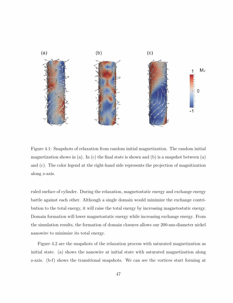
Figure 4.1: Snapshots of relaxation from random initial magnetization. The random initial
magnetization shows in (a). In (c) the final state is shown and (b) is a snapshot between (a)
and (c). The color legend at the right-hand side represents the projection of magnitization
along z-axis.
ruled surface of cylinder. During the relaxation, magnetostatic energy and exchange energy
battle against each other. Although a single domain would minimize the exchange contri-
bution to the total energy, it will raise the total energy by increasing magnetostatic energy.
Domain formation will lower magnetostatic energy while increasing exchange energy. From
the simulation results, the formation of domain closures allows our 200-nm-diameter nickel
nanowire to minimize its total energy.
Figure 4.2 are the snapshots of the relaxation process with saturated magnetization as
initial state. (a) shows the nanowire at initial state with saturated magnetization along
z-axis. (b-f) shows the transitional snapshots. We can see the vortices start forming at
47
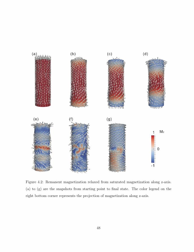
Figure 4.2: Remanent magnetization relaxed from saturated magnetization along z-axis.
(a) to (g) are the snapshots from starting point to final state. The color legend on the
right bottom corner represents the projection of magnetization along z-axis.
48
the two ends of the nanowire while the body center is still generally magnetized along
the easy axis in (b-d). The color legend on the right bottom corner of Figure 4.2 and
the right-hand side of Figure 4.1, represents the projection of magnetization along z-axis.
The magnetization values are the normalized values over saturation magnetization Ms and
between the range of [-1, 1].
To further study the magnetic properties of 200-nm-diameter nickel nanowires, the
magnetic reversal is investigated here. During alignment, the nickel nanowires are magne-
tized by external field, and eventually after alignment, the external field has to be removed.
Here we want to see how the nickel nanowires are magnetized and how the magnetization
of those wires will change after removal of the external field.
A large external magnetic field pointing to +z-direction is applied to the nanowire,
which the external field is along the cylinder axis. The applied external magnetic field is
quite large at the beginning which magnetizes the nanowire to saturation state, Mz = 1
shown in Figure 4.3(a). Then we gradually reduce the external magnetic field, the reversal
process starts by the nucleation of the two ends and subsequently propagates along the
cylinder axis. As the field reduces to 0, the magnetization shown as (d) in which the
magnetic moments forms vortices and the cores of these vortices parallel with cylinder axis.
The field keeps reducing and reaches negative value, and correspondingly the magnetization
of nanowire starts saturating in −z-direction.
For soft magnetic nanowires, there are two basic reversal modes depending on their
thickness, which are known as the vortex wall mode and transverse wall mode. If the fer-
romagnetic nanowires are thin enough, nanowires can be approximated as two dimensional
and the transverse wall mode can be performed. For our nickle nanowire with diameter
200 nm, it is a three dimensional structure and reversal process is in the vortex wall mode.
As we can see, vortices start nucleating at the end of the wire and propagate along the wire
axis. The reason why the domain formation starts at the end is that the demagnetizing
49
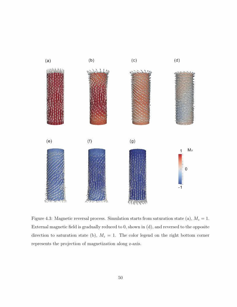
Figure 4.3: Magnetic reversal process. Simulation starts from saturation state (a), Mz = 1.
External magnetic field is gradually reduced to 0, shown in (d), and reversed to the opposite
direction to saturation state (b), Mz = 1. The color legend on the right bottom corner
represents the projection of magnetization along z-axis.
50
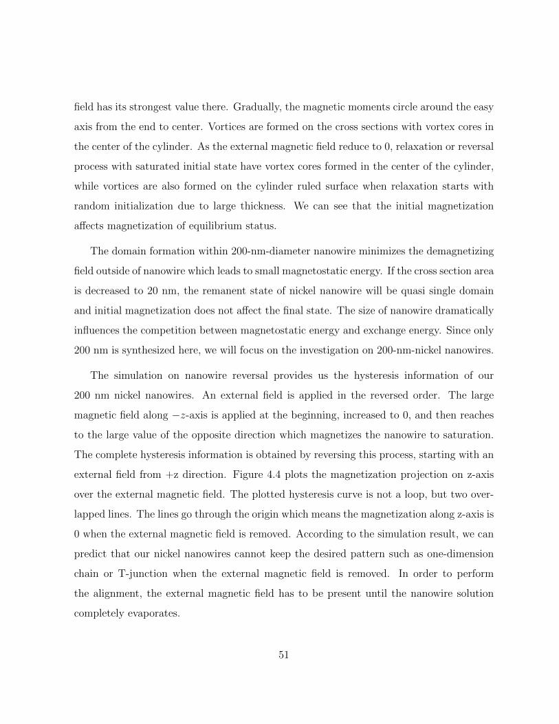
field has its strongest value there. Gradually, the magnetic moments circle around the easy
axis from the end to center. Vortices are formed on the cross sections with vortex cores in
the center of the cylinder. As the external magnetic field reduce to 0, relaxation or reversal
process with saturated initial state have vortex cores formed in the center of the cylinder,
while vortices are also formed on the cylinder ruled surface when relaxation starts with
random initialization due to large thickness. We can see that the initial magnetization
affects magnetization of equilibrium status.
The domain formation within 200-nm-diameter nanowire minimizes the demagnetizing
field outside of nanowire which leads to small magnetostatic energy. If the cross section area
is decreased to 20 nm, the remanent state of nickel nanowire will be quasi single domain
and initial magnetization does not affect the final state. The size of nanowire dramatically
influences the competition between magnetostatic energy and exchange energy. Since only
200 nm is synthesized here, we will focus on the investigation on 200-nm-nickel nanowires.
The simulation on nanowire reversal provides us the hysteresis information of our
200 nm nickel nanowires. An external field is applied in the reversed order. The large
magnetic field along −z-axis is applied at the beginning, increased to 0, and then reaches
to the large value of the opposite direction which magnetizes the nanowire to saturation.
The complete hysteresis information is obtained by reversing this process, starting with an
external field from +z direction. Figure 4.4 plots the magnetization projection on z-axis
over the external magnetic field. The plotted hysteresis curve is not a loop, but two over-
lapped lines. The lines go through the origin which means the magnetization along z-axis is
0 when the external magnetic field is removed. According to the simulation result, we can
predict that our nickel nanowires cannot keep the desired pattern such as one-dimension
chain or T-junction when the external magnetic field is removed. In order to perform
the alignment, the external magnetic field has to be present until the nanowire solution
completely evaporates.
51
Figure 4.4: Hysteresis plot of nickel nanowire with 200 nm diameter. The plotted curve
above is actually two overlapped lines that all go though origin point (0, 0).
52
The magnetic properties of 200 nm diameter nickel nanowire are obtained from previous
simulation results. The relaxation processions and the non-hysteresis property show that
the demagnetizing field outside the nanowire on z-direction is nearly 0 when no external
magnetic field is applied. In order to align the wires in desired order, we have to keep
the external field present until nanowire solution dries out, which will then indicate the
fabricated nanowires will need sustainable external field during the alignment.
4.3 Nanowire Synthesis
The electrodeposition method is used for preparation of the ferromagnetic nanowire and
multisegment nanowire is reported [66]. In this chapter, 200 nm nickel nanowires are
prepared using electrodeposition method.
Commercially available Whatman Anodisc porous alumina has been widely used in
recent nanoscale research, such as templates in nanowire fabrication through electrode-
position. This material has a precise, nondeformable honeycomb pore structure with no
lateral crossovers. Three nominal pore sizes, 20, 100, and 200 nm, can be purchased from
Whatman company. The Anopore porous alumina membranes are manufactured electro-
chemically [67]. The ideal membranes consist of a densely packed regular, hexagonal-
shaped cells with pores in the cell center. Because the thickness of the membranes is about
60 µm, it is difficult to handle the membranes if they are immersed in aqueous solution
without any support. A work electrode for electrodeposition, from which all of the nanorod
growths inside the template, are rooted [68]. As a physical support and work electrode, an
Ag layer needs to be coated on one side of the membranes.
A three-electrode setup is used here. The reference electrode is Ag/AgCl. The counter
electrode is Pt. A layer of Ag deposited on the back side of the membrane serves as the
working electrode. Electrical contact to the Ag is made using a silver plate, which the Ag
53
side of the membrane sits on.
Each membrane pore is first galvanostatically filled with about 20 µm of Ag. Then, Au
is deposited in a chronocoulometry setup using potassium aurocyanide (KAu(CU)2). The
deposition rate of Au in alumina pores is experimentally determined to be 2.25 mC/nm.
For the Nickel part, it is deposited in chronocoulometry setup as well. The plating solution
is purchased commercial product by Technic Inc.. The deposition rate of Ni is 3.37 mC/nm
in the alumina membranes. The last deposition is Ag, which is the same as the first layer
Au deposition.
Surprisingly, the sizes and shapes of the nickel nanowires obtained by etching alumina
membranes with nominal pore sizes of 20 nm and 100 nm are similar to those obtained by
etching alumina membranes with a pore size 200 nm. Since the nominal pore size shows
20 nm, we expect the diameter to be much smaller. In Xiao’s paper [68], it answers why
200 nm nanowires are obtained. Both the top and bottom surfaces of a membrane with
100 nm nominal pore size are imaged. The SEM image of the top surface of a membrane
shows nominal size of 100 nm while the image of the bottom surface shows a totally
different pore size of 200 nm. Cross-section images also shows the pore size of 200 nm even
for membranes with a nominal pore size of ∼20 nm [68]. It shows that the 20 nm and
100 nm diameter pore sizes are defined by thin network layers, beneath which are pores
of 200 nm. For the Whatman membrane, there are two layers: a porous alumina support
layer and an active layer. The support layers have the nominal pore size of 200 nm for
all three types, while the active layers contains smaller size pores. The pore size claimed
by the company is actually the pore size of active layers. In some applications, such as
filters, the hole size of the active layer determines what species can pass. For applications
in nanoscale research, such as metal nanowire growth by electrodeposition, the pores in
alumina support layer is useful. Here we will only investigate the aligning effect of 200 nm
diameter nickel nanowires.
54
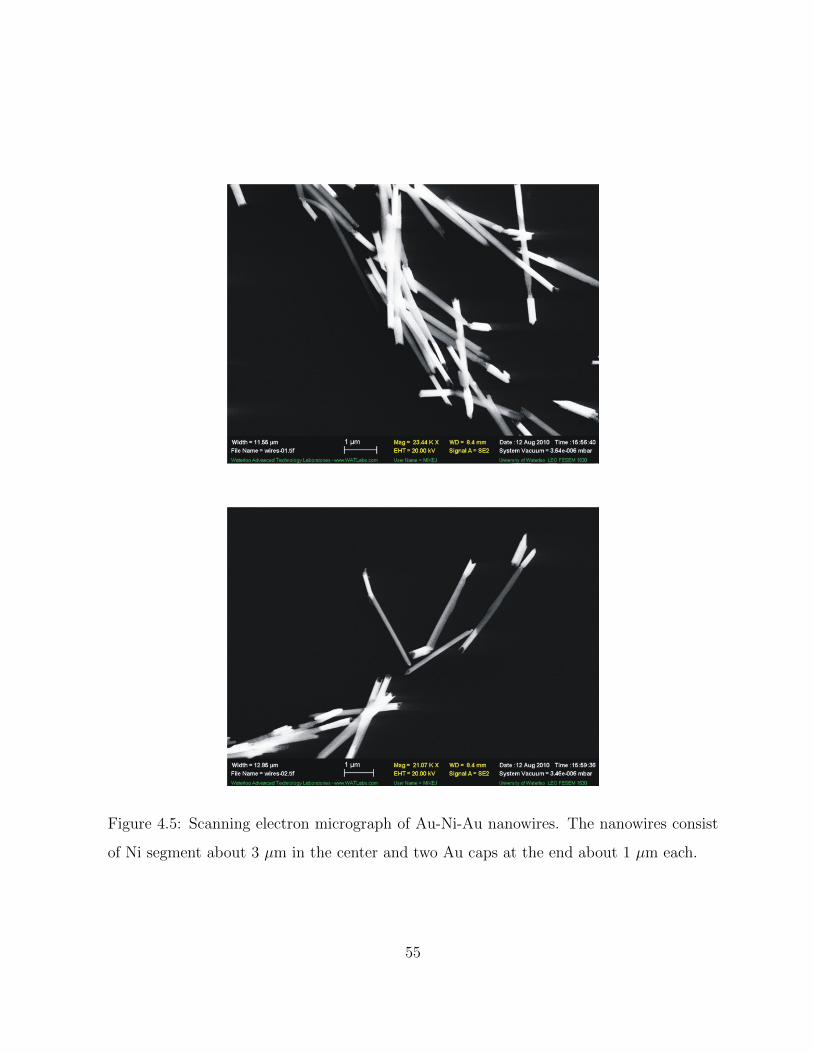
Figure 4.5: Scanning electron micrograph of Au-Ni-Au nanowires. The nanowires consist
of Ni segment about 3 µm in the center and two Au caps at the end about 1 µm each.
55
When the electrodeposition is complete, the alumina membrane containing metal wires
is removed from the electrochemical setup. The deposited Ag on the back side can be
etched using a solution of 0.3 M nitric acid. The Ag etchant also etches Ni but not Au,
thus keeping Au caps at the two ends are necessary to protect Ni segment. The membrane
is immersed in the nitric acid for 10 minutes and the process can be repeated if necessary.
During Ag removal, nanowires are trapped within the alumina membrane and sealed by Au
at the ends. The next step is removing alumina membrane using 3 M sodium hydroxide
(NaOH) which can release the nanowires into the water. Centrifugation after alumina
membrane fully dissolves will separate nanowires from solution. Then replace NaOH with
ethanol and repeat it for 10 times, so the final solvent used for storage of the wires is
ethanol.
For the alignment, the diameter is fixed at 200 nm while we don’t have specific require-
ments on the length of nanowires. Here, the nanowires with Au caps approximately 1 µm
and Ni segment approximately 3 µm were fabricated. The Scanning Electron Microscopy
(SEM) images are shown in Figure 4.5. In some cases, the Au caps are missing from the
ends, which they have fallen off in the solution. One hypothesis is that some Au caps
adjoin with the Ag layer on the back and fell off during etching.
4.4 Two-Dimensional Alignment
Electrostatic [69] and mangetic assembly [70, 71, 72] methods of metal nanowires have been
studied preciously. Two techniques mainly used for self-assembly are free alignments in
fluids and trapping. In magnetic assembly, free alignment in fluid typically includes the a
droplet of a fluid containing magnetic nanowires; manipulation can be achieved by applying
magnetic field (rotating or static). Trapping traditionally involves the addition of patterned
ferromagnetic pads on the substrate, where the magnetic interaction between magnetic
56
nanowires and the ferromangetic pads attracts wires to be aligned [72]. Magnetic alignment
is reported as a facile technique for assembling nanowires into two hierarchical structures.
For the alignment of cross-junctions and T-junctions in this chapter, a sequential alignment
technique on unpatterned substrates under the external magnetic field is used.
With the appropriate applied external magnetic field, two-dimension alignment requires
two steps. The alignments are all carried on a glass slide which is cleaned using an iso-
propanol and ethanol rinse. The first deposition will create one-dimensional chains. In
second alignments, deposited one-dimensional chains behave as ferromagnetic electrodes
for subsequent nanowire alignments. Then the cross-junctions and T-junctions will be
conducted on glass slides. Once a 5 µL droplet containing the nanowire has been placed
on the substrate, then apply an external field. The external magnetic field is present until
the solvent has fully evaporated in the air. The external field is generated by two bar
magnets which are aligned parallel with a 7.5 mm gap in between where the droplet is
placed. The field strength of a single bar magnet is measured to be 500 G at 1 cm from
the magnet surface, and 1000 G at 0.5 cm from the magnet surface. After the droplet fully
evaporates, we rotate the glass slide by 90◦, keeping the two bar magnets aligned with
7.5 mm separation and placing the second 5 µL droplet.
There are several parameters that can be used within this work, such as dilution of wires,
magnetic field strength, volume of the solution pipetted onto substrate, solvent viscosity,
solvent evaporation rate, substrate wettability with solvent and so on. These factors play
important roles on the nanowire travelling speed and travelling time, and strongly affect the
alignment output. In order to disperse the nanowires well on the substrate, the substrate
needs to be larger than the footprint of solvent droplet. A droplet of 5 µL is a reasonable
small volume for our experiment. Ethanol and water are both tried as a solvent. Compared
to water, ethanol has a relatively faster evaporation rate and better wettability on glass. So
a 5 µL ethanol droplet evaporates much faster than water due to the larger droplet surface
57
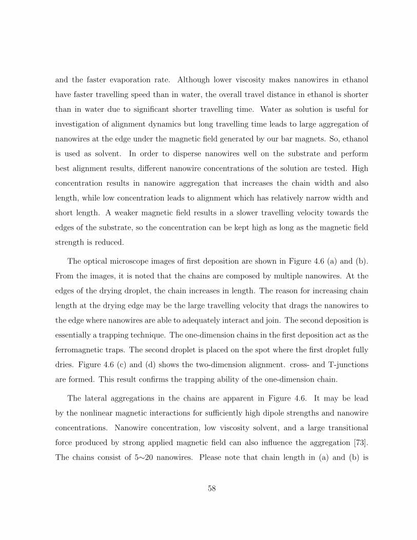
and the faster evaporation rate. Although lower viscosity makes nanowires in ethanol
have faster travelling speed than in water, the overall travel distance in ethanol is shorter
than in water due to significant shorter travelling time. Water as solution is useful for
investigation of alignment dynamics but long travelling time leads to large aggregation of
nanowires at the edge under the magnetic field generated by our bar magnets. So, ethanol
is used as solvent. In order to disperse nanowires well on the substrate and perform
best alignment results, different nanowire concentrations of the solution are tested. High
concentration results in nanowire aggregation that increases the chain width and also
length, while low concentration leads to alignment which has relatively narrow width and
short length. A weaker magnetic field results in a slower travelling velocity towards the
edges of the substrate, so the concentration can be kept high as long as the magnetic field
strength is reduced.
The optical microscope images of first deposition are shown in Figure 4.6 (a) and (b).
From the images, it is noted that the chains are composed by multiple nanowires. At the
edges of the drying droplet, the chain increases in length. The reason for increasing chain
length at the drying edge may be the large travelling velocity that drags the nanowires to
the edge where nanowires are able to adequately interact and join. The second deposition is
essentially a trapping technique. The one-dimension chains in the first deposition act as the
ferromagnetic traps. The second droplet is placed on the spot where the first droplet fully
dries. Figure 4.6 (c) and (d) shows the two-dimension alignment. cross- and T-junctions
are formed. This result confirms the trapping ability of the one-dimension chain.
The lateral aggregations in the chains are apparent in Figure 4.6. It may be lead
by the nonlinear magnetic interactions for sufficiently high dipole strengths and nanowire
concentrations. Nanowire concentration, low viscosity solvent, and a large transitional
force produced by strong applied magnetic field can also influence the aggregation [73].
The chains consist of 5∼20 nanowires. Please note that chain length in (a) and (b) is
58
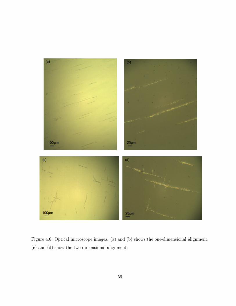
Figure 4.6: Optical microscope images. (a) and (b) shows the one-dimensional alignment.
(c) and (d) show the two-dimensional alignment.
59
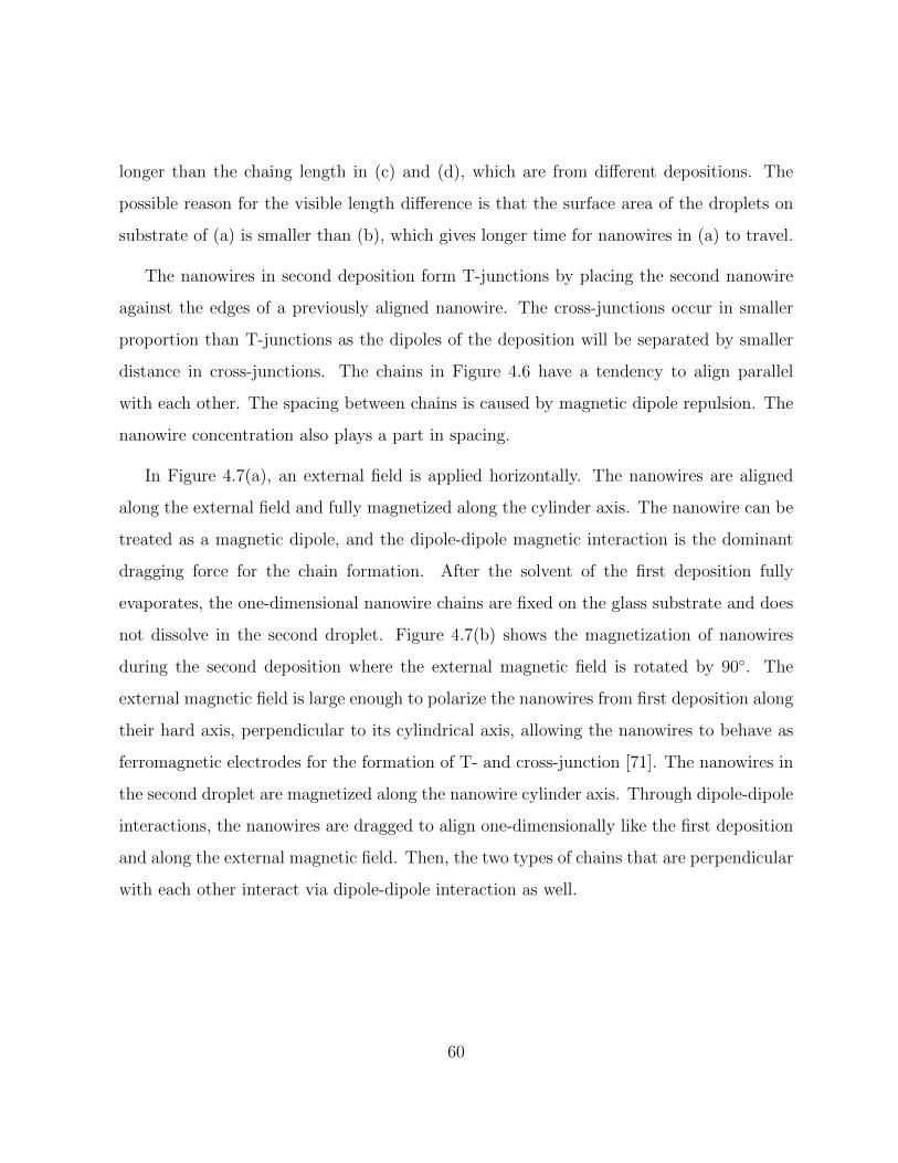
longer than the chaing length in (c) and (d), which are from different depositions. The
possible reason for the visible length difference is that the surface area of the droplets on
substrate of (a) is smaller than (b), which gives longer time for nanowires in (a) to travel.
The nanowires in second deposition form T-junctions by placing the second nanowire
against the edges of a previously aligned nanowire. The cross-junctions occur in smaller
proportion than T-junctions as the dipoles of the deposition will be separated by smaller
distance in cross-junctions. The chains in Figure 4.6 have a tendency to align parallel
with each other. The spacing between chains is caused by magnetic dipole repulsion. The
nanowire concentration also plays a part in spacing.
In Figure 4.7(a), an external field is applied horizontally. The nanowires are aligned
along the external field and fully magnetized along the cylinder axis. The nanowire can be
treated as a magnetic dipole, and the dipole-dipole magnetic interaction is the dominant
dragging force for the chain formation. After the solvent of the first deposition fully
evaporates, the one-dimensional nanowire chains are fixed on the glass substrate and does
not dissolve in the second droplet. Figure 4.7(b) shows the magnetization of nanowires
during the second deposition where the external magnetic field is rotated by 90◦. The
external magnetic field is large enough to polarize the nanowires from first deposition along
their hard axis, perpendicular to its cylindrical axis, allowing the nanowires to behave as
ferromagnetic electrodes for the formation of T- and cross-junction [71]. The nanowires in
the second droplet are magnetized along the nanowire cylinder axis. Through dipole-dipole
interactions, the nanowires are dragged to align one-dimensionally like the first deposition
and along the external magnetic field. Then, the two types of chains that are perpendicular
with each other interact via dipole-dipole interaction as well.
60
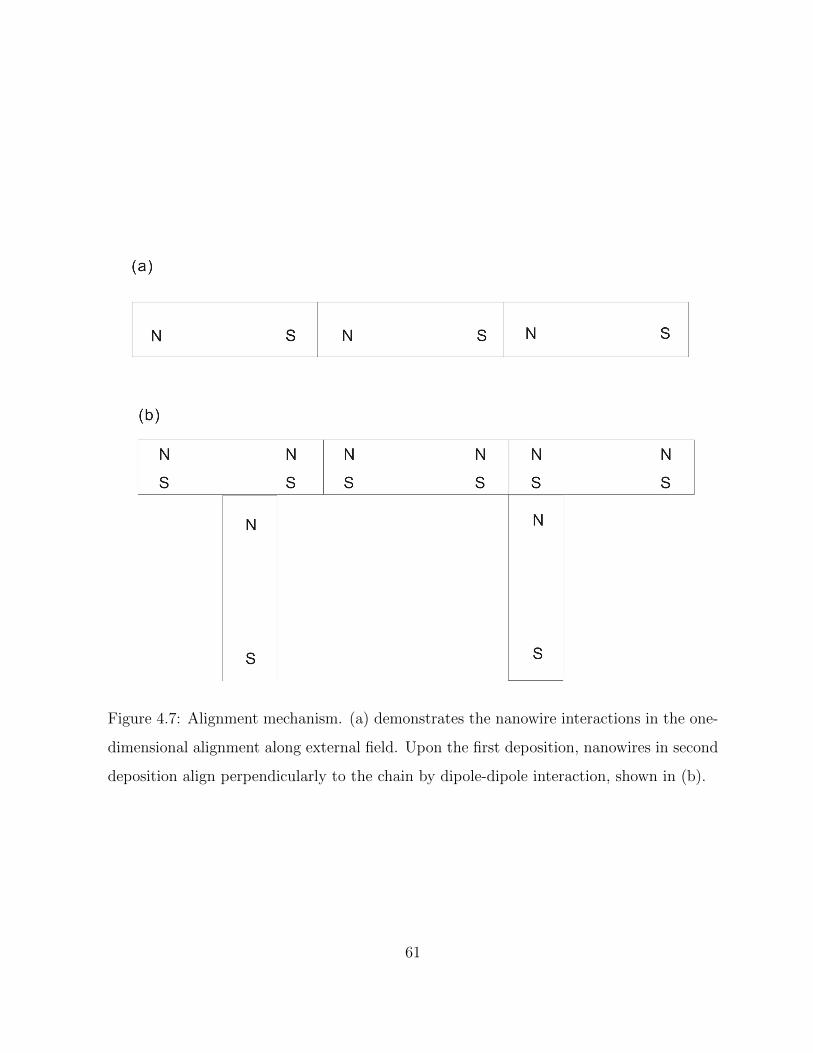
Figure 4.7: Alignment mechanism. (a) demonstrates the nanowire interactions in the one-
dimensional alignment along external field. Upon the first deposition, nanowires in second
deposition align perpendicularly to the chain by dipole-dipole interaction, shown in (b).
61
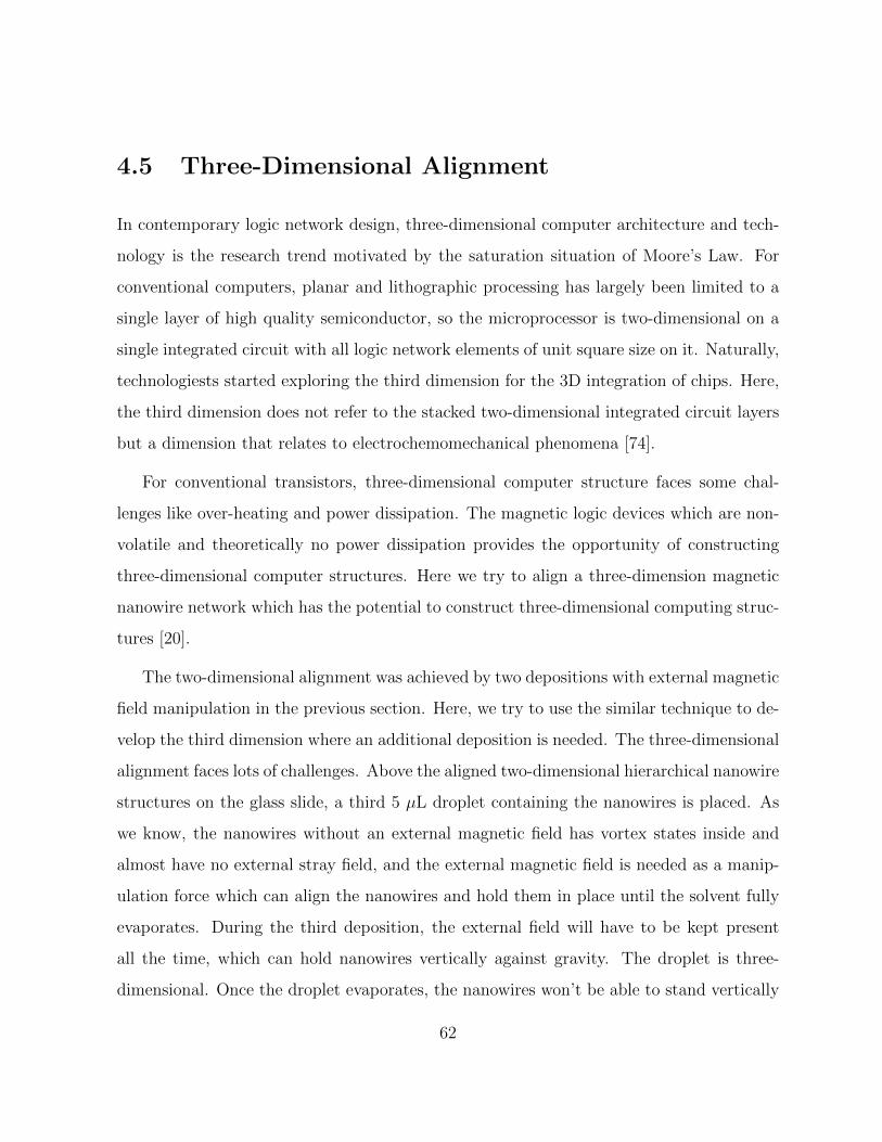
4.5 Three-Dimensional Alignment
In contemporary logic network design, three-dimensional computer architecture and tech-
nology is the research trend motivated by the saturation situation of Moore’s Law. For
conventional computers, planar and lithographic processing has largely been limited to a
single layer of high quality semiconductor, so the microprocessor is two-dimensional on a
single integrated circuit with all logic network elements of unit square size on it. Naturally,
technologiests started exploring the third dimension for the 3D integration of chips. Here,
the third dimension does not refer to the stacked two-dimensional integrated circuit layers
but a dimension that relates to electrochemomechanical phenomena [74].
For conventional transistors, three-dimensional computer structure faces some chal-
lenges like over-heating and power dissipation. The magnetic logic devices which are non-
volatile and theoretically no power dissipation provides the opportunity of constructing
three-dimensional computer structures. Here we try to align a three-dimension magnetic
nanowire network which has the potential to construct three-dimensional computing struc-
tures [20].
The two-dimensional alignment was achieved by two depositions with external magnetic
field manipulation in the previous section. Here, we try to use the similar technique to de-
velop the third dimension where an additional deposition is needed. The three-dimensional
alignment faces lots of challenges. Above the aligned two-dimensional hierarchical nanowire
structures on the glass slide, a third 5 µL droplet containing the nanowires is placed. As
we know, the nanowires without an external magnetic field has vortex states inside and
almost have no external stray field, and the external magnetic field is needed as a manip-
ulation force which can align the nanowires and hold them in place until the solvent fully
evaporates. During the third deposition, the external field will have to be kept present
all the time, which can hold nanowires vertically against gravity. The droplet is three-
dimensional. Once the droplet evaporates, the nanowires won’t be able to stand vertically
62
and are going to fall down on the glass slide. Even with external field generated by the bar
magnet, the third dimension alignment will still collapse as solvent evaporates and droplet
surface lowers.
Next, we make attempts to maintain standing position of nanowires even when the
external field is removed. Our goal is that the third dimension chains can be sustained
in solvent after removal of the external magnetic field. Here, the solvent viscosity plays
an important role. Within a high viscosity solvent, the random thermal motion can be
reduced, and even motion caused by gravity could be eliminated. The viscosity needed
to sustain the third dimension standing is unknown to us. There are two ways to find
the desired viscosity range. One is to try various materials with different viscosities as
solvents. The other is to use one material by manipulating its viscosity. The second option
can provide continuous viscosity variations and give more flexibility, so one material was
used in our three-dimensional alignment and the viscosity was controlled over temperature
manipulation.
In previous sections, ethanol and water were tried as solvents. Ethanol evaporates
fast and 5 ml ethanol can easily evaporate before the required experiment conditions are
reached or before the three-dimensional alignment is observed. Once droplet is about to
dry out, the surface tension will destroy the vertical alignment. Water is a good candidate
for solvent which provides wide controllable viscosity and low evaporation rate. Water
viscosity data obtained from Dortmund Data Bank [75] shows a wide range of viscosity
with various temperatures.
Dynamic water viscosity data are plotted in Figure 4.8 with the viscosity as y-axis and
temperature as x-axis. High viscosity can be achieved by lowering the temperature. Peltier
cooler is a solid-state active heat pump which transfers heat from one side of the device
to the other side with consumption of electrical power. The peltier cooler with small size
and flat shape fits under the glass slide very well and we can use its cooling effect in our
63
Figure 4.8: Dynamic viscosity of water (data obtained from DDB [75]). Dynamic viscos-
ity is also called absolute viscosity. This plot lists viscosity of liquid water at different
temperatures. In this section, only viscosity of liquid water is needed.
third alignment. At room temperature, water viscosity is not high enough to hold the third
dimensional chain, and low viscosity is desired. Peltier cooler performance is a function
of ambient temperatures. The typical maximum temperature difference between the hot
side and cold side is 70◦. To achieve low temperature, the hot side should maintain proper
temperature. A cooling kit for heat dissipation is needed to prevent the hot side from
overheating.
The main challenges faced by three-dimensional alignment are the observation of the
third dimension. The precious planar nanowire alignments can be observed by optical
64
microscope or scanning electron microscope. For use of scanning electron microscope, the
specimen chamber must be kept at high vacuum level, and the specimen should normally
be completely dry, so scanning electron microscope is ruled out for alignment observation.
For optical microscope use, the slight angle of the vertical external magnetic field will be
able make the third dimension alignment observable. Under standard atmosphere, water
solidifies at 0◦ and vertical nanowires will stay aligned. But the frost on the droplet surface
prevents will create great difficulties of observation. Further development is needed for this
part.
4.6 Summary
In this chapter, we studied the magnetic properties of nickel nanowires and their alignment.
We investigated their magnetic remanent states and response to external magnetic field
by means of micromagnetic simulations. Vortices were formed in the 200-nm-diameter
nickel nanowires when no external field was applied, and the demagnetizing field returned
to zero as well. In order to align the wires in the desired order. Deposited nanowires,
which were aligned in an external field and fixed on a glass substrate, could serve as
’traps’ for subsequent depositions of nickel nanowires. This trapping strategy gave the
alignment the ability to form different two-dimensional structures, such as cross-junctions
and T-junctions demonstrated in this thesis. Three-dimensional alignment was attempted
as well. The same trapping concept was applied for the vertical alignment. Water was
used as solvent in the third deposition to facilitate the vertical alignment of the nanowires.
The high viscosity of the solvent was achieved by reducing the temperature.
65
Chapter 5
Conclusions and Future Work
5.1 Summary
Magnetic devices are highly attractive. They have the potential to achieve programmable
and non-volatile logic functions, magnetic recording, and micromagnetic and spintronics
sensors.
In this thesis, I established geometrical stability criteria for S-shaped elements by
performing micromagnetic simulations. The geometric parameters of S-shaped elements
played an important role in stabilizing the desired logic functionality. The detailed micro-
magnetic analysis of geometrical parameter space was presented. The two appendages give
the biasing effect which made the coercive field shift. This coercive field shift is the basis
of S-shaped element logic functionality. Geometrical criteria, like the size and aspect ratio
of the center rectangular prism and appendages, are critical for logic operation. The center
rectangular prism with a maximum width of 125 nm and minimum length of 190 nm is a
good choice that can suppress flux-closure magnetization patterns. Appendages with an
area between 1000 and 2000 nm2 and an aspect ratio of up to 5/3 offer the appropriate
effect for coercive field biasing.
66
Devices constructed by magnetic nanowires may have a wide spectrum of applications in
the future. In order to build ordered structures, magnetic fields were used as an external
stimulus force for nickel nanowire ordering. In this thesis, the magnetic behaviour of
200-nm-diameter nickel nanowires was investigated by micromagnetic simulations and by
experiments. The vortex formation in the cylinder minimizes the overall energy, so that
the demagnetizing field outside the nanowire was very small. This, in turn, prevents
nanowires from self-ordering. Nickel nanowires with a diameter of 200 nm were synthesized
by eletrodeposition into alumina pores. One-dimensional and two-dimensional alignment
on a glass substrate was successfully performed and observed. Synthesized nanowires were
diluted and stored in ethanol solvent for one-dimensional and two-dimensional alignment.
First, a 5 µL droplet containing nanowires was placed onto a glass substrate in an external
magnetic field. Then, a second 5 µL droplet was placed on top of the first one with
a perpendicular external magnetic field present. Structures like T-junctions and cross-
junctions were achieved. We attempted to add a vertical dimension on the two-dimensional
structures by systematically varying the solvent viscosity. Viscosities of water and ethanol
increase as the temperature drops. Hence, below a certain temperature, solvent viscosity
should be large enough to hold the vertical alignment against gravity.
5.2 Future Work
The presented work on S-state reconfigurable magnetic logic devices was simulation-based.
The next step is device fabrication. A large block of S-shaped elements with various geo-
metrical parameters can be placed on a substrate with reasonable distance, and magnetic
force microscope can be used to observe the magnetization of the elements. With S-state
reconfigurable magnetic logic devices fabricated, the geometrical space identified by simu-
lations can be experimentally verified.
67
Apart from S-state reconfigurable magnetic logic devices, nanostructures like ring struc-
tures, C-shaped structures, L-shaped structures, triangle structures and so on may be mod-
ified and configured as reconfigurable logic devices as well. These structures need to have
a square-like hysteresis loop with abrupt switching behaviour and biasing parts that give
coercive shifts. Consequently, their geometrical space could be investigated by simulations
and ultimately experiments.
We attempted the three-dimensional alignment of Ni nanowires by varying the solvent
viscosity. Observation difficulties and temperature control flexibility issues need to be
solved for achieving alignment in the third dimension.
68
Bibliography
[1] R. R. Schaller, “Moore’s law: past, present, and future,” IEEE Spectr., vol. 34, pp. 52–
59, June 1997.
[2] O. Shacham, O. Azizi, M. Wachs, W. Qadeer, Z. Asgar, K. Kelley, J. Stevenson,
S. Richardson, M. Horowitz, B. Lee, A. Solomatnikov, and A. Firoozshahian, “Re-
thinking digital design: Why design must change,” Micro, IEEE, vol. 30, pp. 9 –24,
nov.-dec. 2010.
[3] W. C. Black and B. Das, “Programmable logic using giant-magnetoresistance and
spin-dependent tunneling devices (invited),” J. Appl. Phys., vol. 87, pp. 6674–6679,
2000.
[4] A. Jaecklin, “A multiaperture magnetic control device,” Magnetics, IEEE Transac-
tions on, vol. 2, pp. 356 – 359, Sept. 1966.
[5] H. Gschwind, Design of Digital Computers. New York, NY: Springer Verlag, 1967.
[6] A. Imre, G. Csaba, L. Ji, A. Orlov, G. Bernstein, and W. Porod, “Majority logic gate
for magnetic quantum-dot cellular automata,” Science, vol. 311, pp. 205–208, Jan 13
2006.
69
[7] A. Imre, Experimental study of nanomagnets for magnetic quantum dot cellular au-
tomata (mQCA) logic applications. PhD thesis, University of Notre Dame, South
Bend, IN, 2005.
[8] P. L. G. Csaba and W. Porod, “Power dissipation in nanomagnetic logic devices,”
pp. 346 – 348, aug. 2004.
[9] H. W. Schumacher, C. Chappert, R. C. Sousa, and P. P. Freitas, “Effective bit ad-
dressing times for precessional switching of magnetic memory cells,” Journal of Applied
Physics, vol. 97, no. 12, p. 123907, 2005.
[10] R. P. Cowburn, “Where have all the transistors gone?,” Science, vol. 311, no. 5758,
pp. 183–184, 2006.
[11] M. Meyyappan and M. K. Sunkara, Inorganic Nanowires: Applications, Properties,
and Characterization. Boca Raton, FL, USA: CRC Press, 2010.
[12] Y. Cui, Z. Zhong, D. Wang, W. U. Wang, and C. Lieber, “High performance silicon
nanowire field effect transistors,” Nano Lett., vol. 3, pp. 149–152, Nov 2003.
[13] H. Y. Cha, H. Wu, S. Chae, and M. G. Spencer, “Gallium nitride nanowire nonvolatile
memory device,” J. Appl. Phys., vol. 100, no. 2, p. 024307, 2006.
[14] M. H. Huang, S. Mao, H. Feick, H. Yan, Y. Wu, H. Kind, E. Weber, R. Russo,
and P. Yang, “Room-temperature ultraviolet nanowire nanolasers,” Science, vol. 292,
no. 5523, pp. 1897–1899, 2001.
[15] K. Kalantar-zadeh and B. Fry, Magneitc Domains: The Analysis of Magnetic Mi-
crostructures. Springer, 1998.
70
[16] S. Kato, S. Nigo, Y. Uno, T. Onisi, and G. Kido, “Voltage-induced insulator-metal
transition at room temperature in an anodic porous alumina thin film,” Journal of
Physics: Conference Series, vol. 38, no. 1, p. 148, 2006.
[17] Y. G. Guo, L. J. Wan, C. F. Zhu, D. L. Yang, D. M. Chen, and C. L. Bai, “Ordered
ni-cu nanowire array with enhanced coercivity,” Chem. Mater., vol. 15, pp. 664–667,
2003.
[18] D. A. Allwood, G. Xiong, M. D. Cooke, C. C. Faulkner, D. Atkinson, N. Vernier, and
R. P. Cowburn, “Submicrometer ferromagnetic not gate and shift register,” Science,
vol. 296, no. 5575, pp. 2003–2006, 2002.
[19] V. Rodrigues, J. Bettini, P. C. Silva, and D. Ugarte, “Evidence for spontaneous spin-
polarized transport in magnetic nanowires,” Phys. Rev. Lett., vol. 91, p. 096801, Aug
2003.
[20] S. N. Yanushkevich, V. P. Shmerko, and E. Sergey, Logic Design of NanoICs. Boca
Raton, FL, USA: CRC Press, 2005.
[21] C. M. Hangarter, Y. Rheem, B. Yoo, E.-H. Yang, and N. V. Myung, “Hierarchical
magnetic assembly of nanowires,” Nanotechnology, vol. 18, no. 20, p. 205305, 2007.
[22] G. Snider and W. Robinett, “Crossbar demultiplexers for nanoelectronics based on
n-hot codes,” Nanotechnology, IEEE Transactions on, vol. 4, pp. 249 – 254, march
2005.
[23] A. Hubert and R. Schafer, Magneitc Domains: The Analysis of Magnetic Microstruc-
tures. Springer, 1998.
[24] W. Heisenberg, “On the theory of ferromagnetism,” Z. Phys., vol. 49, p. 619, 1928.
71
[25] N. Spaldin, Magnetic Materials: Fundamentals and Device Applications. Cambridge
University Press, 2003.
[26] R. Boardman, Computer simulation studies of magnetic nanostructures. Ph.D. thesis,
University of Southampton, 2005.
[27] B. S. Oxford University Press, 1st edition ed., 2001.
[28] W. F. Brown, Micromagnetics. New York: Wiley, 1963.
[29] L. Landau and E. Liftshits, “On the theory of the dispersion of magnetic permeability
in ferromagnetic bodies,” Phys. Zeitsch. der Sow., vol. 8, pp. 153–169, 1928.
[30] R. H. Engel-Herbert, Micromagnetic study of self-organized magnetic nanostructures.
Ph.D. thesis, Humboldt-University, 2005.
[31] E. D. Dahlberg and J. G. Zhu, “Micromagnetic microscopy and modeling,” Physics
Today, vol. 18, pp. 34–40, 1995.
[32] G. Pelosi, “The finite-element method, part i: R. l. courant [historical corner],” An-
tennas and Propagation Magazine, IEEE, vol. 49, pp. 180–182, 2007.
[33] R. Engel-Herbert, T. Hesjedal, J. Mohanty, D. M. Schaadt, and K. H. Ploog, “Magne-
tization reversal in mnas films: Magnteic force microscopy, squid magnetometry, and
micromagnetic simulations,” Phys. Rev. B, vol. 73, p. 104441, 2006.
[34] R. Cowburn and M. Welland, “Room temperature magnetic quantum cellular au-
tomata,”
[35] G. Csaba and W. Porod, “Simulation of field-coupled computing architectures based
on magnetic dot arrays,” J. Comput. Electr., vol. 1, pp. 87–91, 2002.
72
[36] S. Haque, M. Yamamoto, R. Nakatani, and Y. Endo, “Binary logic gates by ferromag-
netic nanodots,” J. Magn. Magn. Mater., vol. 282, pp. 380–384, Nov 1 2004.
[37] L. Gross, R. R. Schlittler, G. Meyer, and R. Allenspach, “Magnetologic devices fabri-
cated by nanostencil lithography,” Nanotechnology, vol. 21, p. 325301, Aug 13 2010.
[38] A. Ney, C. Pampuch, R. Koch, and K. Ploog, “Programmable computing with a single
magnetoresistive element,” Nature, vol. 425, pp. 485–487, Oct 2 2003.
[39] B. Behin-Aein, D. Datta, S. Salahuddin, and S. Datta, “Proposal for an all-spin logic
device with built-in memory,” Nat. Nanotechnol., vol. 5, pp. 266–270, Apr 2010.
[40] G. Prenat, B. Dieny, W. Guo, M. El Baraji, V. Javerliac, and J.-P. Nozieres, “Beyond
MRAM, CMOS/MTJ integration for logic components,” Magnetics, IEEE Transac-
tions on, vol. 45, pp. 3400 –3405, oct. 2009.
[41] H. D. C. David R. Bennion and D. Nitzan, Digital magnetic logic. New York, USA:
McGraw-Hill, 1969.
[42] B. Behin-Aein, S. Salahuddin, and S. Datta, “Switching Energy of Ferromagnetic
Logic Bits,” IEEE Trans. Nanotechnol., vol. 8, pp. 505–514, Jul 2009.
[43] L. Hu and T. Hesjedal unpublished, 2011.
[44] S. Haque, M. Yamamoto, R. Nakatani, and Y. Endo, “Magnetic logic gate for binary
computing,” Sci. Technol. Adv. Mater., vol. 5, pp. 79–82, Jan-Mar 2004.
[45] S. Haque, M. Yamamoto, R. Nakatani, and Y. Endo, “Binary logic gates by ferromag-
netic nanodots,” J. Magn. Magn. Mater., vol. 282, pp. 380–384, Nov 1 2004.
[46] C. Pampuch, A. Das, A. Ney, L. Daweritz, R. Koch, and K. Ploog, “Magnetologic
with alpha-MnAs thin films,” Phys. Rev. Lett., vol. 91, p. 147203, Oct 3 2003.
73
[47] T. Hesjedal and T.Phung, “Magnetic logic element based on an s-shaped permalloy
structure,” Appl. Phys. Lett., vol. 96, p. 072501, 2010.
[48] J. Daughton, “Magnetoresistive memory technology,” Thin Solid Films, vol. 216,
pp. 162–168, Aug 1992.
[49] S. S. P. Parkin, K. P. Roche, M. G. Samant, P. M. Rice, R. B. Beyers, R. E. Scheuerlein,
E. J. OSullivan, S. L. Brown, J. Bucchigano, D. W. Abraham, Y. Lu, M. Rooks, P. L.
Trouilloud, R. A. Wanner, and W. J. Gallagher, “Exchange-biased magnetic tunnel
junctions and application to nonvolatile magnetic random access memory (invited),”
Journal of Applied Physics, vol. 85, pp. 5828 –5833, apr 1999.
[50] P. J. Strachan, Time-resolved x-ray imaging of magnetic nanostructures driven by
spin-transfer torque. Ph.D. thesis, Stanford University, 2007.
[51] S. Parkin, “Giant Magnetoresistance In Magnetic Nanostructures,” Annu. Rev. Mater.
Sci., vol. 25, pp. 357–388, 1995.
[52] J. S. Moodera, L. R. Kinder, T. M. Wong, and R. Meservey, “Large magnetoresistance
at room temperature in ferromagnetic thin film tunnel junctions,” Phys. Rev. Lett.,
vol. 74, pp. 3273–3276, Apr 1995.
[53] T. M. Maffitt, J. K. DeBrosse, J. A. Gabric, E. T. Gow, M. C. Lamorey, J. S. Par-
enteau, D. R. Willmott, M. A. Wood, and W. J. Gallagher, “Design considerations for
MRAM,” IBM Journal of Research and Development, vol. 50, pp. 25 –39, jan. 2006.
[54] H. Kim, J. Lee, I. Baek, Y. Ha, J. Bae, S. Oh, S. Park, U.-I. Chung, N. Lee, H. Kang,
and J. Moon, “Key factors to enhance the switching characteristics in submicron
MRAM cells,” Magnetics, IEEE Transactions on, vol. 40, pp. 2616 – 2618, july 2004.
[55] J. Deak, “Influence of pinned-layer dispersion on magnetic tunnel junction switching
distributions,” Magnetics, IEEE Transactions on, vol. 43, pp. 2821 –2823, june 2007.
74
[56] D. Allwood, N. Vernier, G. Xiong, M. Cooke, D. Atkinson, C. Faulkner, and R. Cow-
burn, “Shifted hysteresis loops from magnetic nanowires,” Appl. Phys. Lett., vol. 81,
pp. 4005–4007, Nov 18 2002.
[57] M. R. Scheinfein, “LLG Micromagnetic Simulator.” http://llgmicro.home.
mindspring.com, 2010. [Online; accessed 24-December-2010].
[58] R. Hertel, “Thickness dependence of magnetization structures in thin Permalloy rect-
angles,” Z. Metallk., vol. 93, pp. 957–962, Oct 2002.
[59] G. Autes, J. Mathon, and A. Umerski, “Oscillatory behavior of tunnel magnetore-
sistance in a magnetic tunnel junction with varying magnetic layer thickness,” Phys.
Rev. B, vol. 84, p. 134404, Oct 2011.
[60] M. Herrmann, S. McVitie, and J. Chapman, “Investigation of the influence of edge
structure on the micromagnetic behavior of small magnetic elements,” J. Appl. Phys.,
vol. 87, pp. 2994–2999, Mar 15 2000.
[61] B. B. Maranville, R. D. McMichael, and D. W. Abraham, “Variation of thin film edge
magnetic properties with patterning process conditions in ni[sub 80]fe[sub 20] stripes,”
Applied Physics Letters, vol. 90, no. 23, p. 232504, 2007.
[62] M. Zhu and R. D. McMichael, “Modification of edge mode dynamics by oxidation
in ni[sub 80]fe[sub 20] thin film edges,” Journal of Applied Physics, vol. 107, no. 10,
p. 103908, 2010.
[63] R. D. McMichael and B. B. Maranville, “Edge saturation fields and dynamic edge
modes in ideal and nonideal magnetic film edges,” Phys. Rev. B, vol. 74, p. 024424,
Jul 2006.
[64] M. Hosomi, H. Yamagishi, T. Yamamoto, K. Bessho, Y. Higo, K. Yamane, H. Yamada,
M. Shoji, H. Hachino, C. Fukumoto, H. Nagao, and H. Kano, “A novel nonvolatile
75
memory with spin torque transfer magnetization switching: Spin-RAM,” in IEEE Int.
Elect. Devices Meeting, International Electron Devices Meeting, pp. 473–476, 2005.
[65] K. Nielsch, R. B. Wehrspohn, J. Barthel, J. Kirschner, U. Gosele, S. F. Fischer, and
H. Kronmuller, “Hexagonally ordered 100 nm period nickel nanowire arrays,” Applied
Physics Letters, vol. 79, no. 9, pp. 1360–1362, 2001.
[66] B. R. Martin, D. J. Dermody, B. D. Reiss, M. Fang, L. A. Lyon, M. J. Natan, and T. E.
Mallouk, “Orthogonal self-assembly on colloidal gold-platinum nanorods,” Advanced
Materials, vol. 11, no. 12, pp. 1021–1025, 1999.
[67] “Anopore inorganic membranes (anodisc) @ONLINE.”
[68] Z. L. Xiao, C. Y. Han, U. Welp, H. H. Wang, W. K. Kwok, G. A. Willing, J. M. Hiller,
R. E. Cook, D. J. Miller, and G. W. Crabtree, “Fabrication of alumina nanotubes
and nanowires by etching porous alumina membranes,” Nano Letters, vol. 2, no. 11,
pp. 1293–1297, 2002.
[69] P. A. Smith, C. D. Nordquist, T. N. Jackson, T. S. Mayer, B. R. Martin, J. Mbindyo,
and T. E. Mallouk, “Electric-field assisted assembly and alignment of metallic
nanowires,” Applied Physics Letters, vol. 77, no. 9, pp. 1399–1401, 2000.
[70] M. Tanase, L. A. Bauer, A. Hultgren, D. M. Silevitch, L. Sun, D. H. Reich, P. C.
Searson, and G. J. Meyer, “Magnetic Alignment of Fluorescent Nanowires,” Nano
Letters, vol. 1, pp. 155–158, Mar. 2001.
[71] C. M. Hangarter and N. V. Myung, “Magnetic alignment of nanowires,” Chemistry of
Materials, vol. 17, no. 6, pp. 1320–1324, 2005.
[72] A. K. Bentley, J. S. Trethewey, A. B. Ellis, and W. C. Crone, “Magnetic manipulation
of coppertin nanowires capped with nickel ends,” Nano Letters, vol. 4, no. 3, pp. 487–
490, 2004.
76
[73] S. Chikazumi and C. Graham. Oxford University Press, 2nd edition ed., 1997.
[74] S. N. Yanushkevich, “Logic design of computational nanostructure,” J. Computational
and Theoretical Nanoscience, vol. 4, no. 3, pp. 467–481, 2007.
[75] J. Gmehling, J. Rarey, and J. Menke, “Dortmund data bank, oldenburg.” http:
//www.ddbst.com/, 2011.
77

![Modelling of multipurpose spintronic devices · magnetic random access memories (MRAM) required a magnetic field to write the logic state in the memory cells [11,13]. This caused](https://img.pdfslide.net/doc/110x75/60502f0d19e64d4f2151d5a1/modelling-of-multipurpose-spintronic-devices-magnetic-random-access-memories-mram.jpg)