Embed Size (px)
Citation preview
Switching Regulators
-1-
S W I T C H I N G R E G U L A T O R S
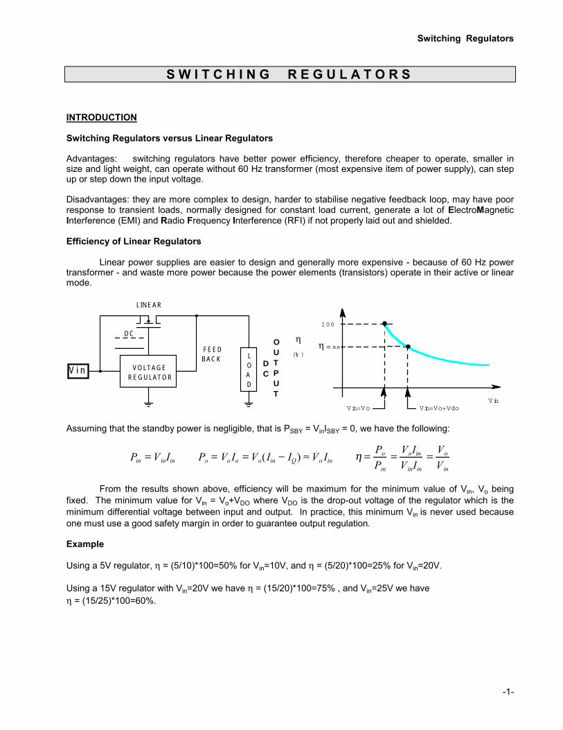
INTRODUCTION Switching Regulators versus Linear Regulators Advantages: switching regulators have better power efficiency, therefore cheaper to operate, smaller in size and light weight, can operate without 60 Hz transformer (most expensive item of power supply), can step up or step down the input voltage. Disadvantages: they are more complex to design, harder to stabilise negative feedback loop, may have poor response to transient loads, normally designed for constant load current, generate a lot of ElectroMagnetic Interference (EMI) and Radio Frequency Interference (RFI) if not properly laid out and shielded. Efficiency of Linear Regulators Linear power supplies are easier to design and generally more expensive - because of 60 Hz power transformer - and waste more power because the power elements (transistors) operate in their active or linear mode.
LOAD
Vi n VOLTAGEREGULATOR
DC
FEEDBACK
LINEAR
DC
OUTPUT
Vin=VoVin
η(% )
100
Vin=Vo+Vdo
η m ax
Assuming that the standby power is negligible, that is PSBY = VinISBY = 0, we have the following:
Pin = VinIin Po = Vo Io = Vo(Iin − IQ) ≈ Vo Iin η = PoPin
= VoIinVinIin
= VoVin
From the results shown above, efficiency will be maximum for the minimum value of Vin, Vo being fixed. The minimum value for Vin = Vo+VDO where VDO is the drop-out voltage of the regulator which is the minimum differential voltage between input and output. In practice, this minimum Vin is never used because one must use a good safety margin in order to guarantee output regulation. Example Using a 5V regulator, η = (5/10)*100=50% for Vin=10V, and η = (5/20)*100=25% for Vin=20V. Using a 15V regulator with Vin=20V we have η = (15/20)*100=75% , and Vin=25V we have η = (15/25)*100=60%.
Switching Regulators
-2-
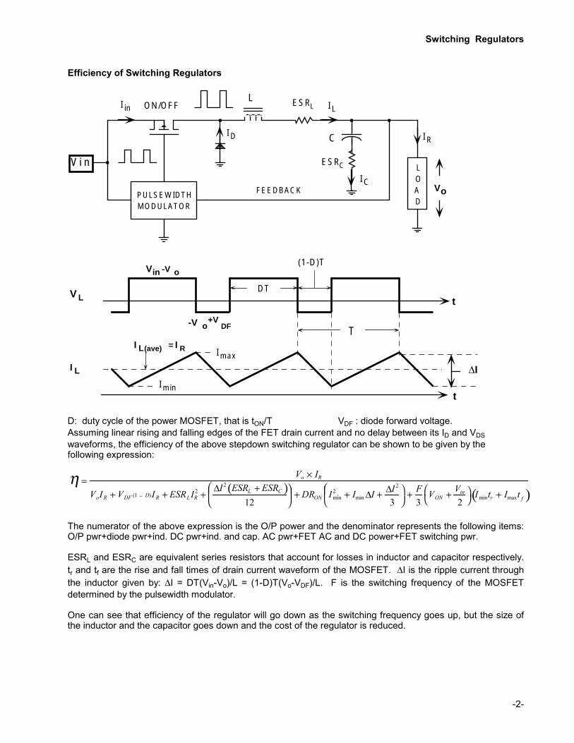
Efficiency of Switching Regulators
ON/OFF
FEEDBACK
LOAD
Vi n
PULSEWIDTHMODULATOR
ESRL
ESRC
C
L
IR
IL
IC
I in
ID
Vo
V L
-V o+V
DF
Vin -V o
I L
Imax
Imin
∆I
I L(ave) = I R
t
tDT
(1-D)T
T
D: duty cycle of the power MOSFET, that is tON/T VDF : diode forward voltage. Assuming linear rising and falling edges of the FET drain current and no delay between its ID and VDS waveforms, the efficiency of the above stepdown switching regulator can be shown to be given by the following expression: η =
Vo × IR
VoIR + VDF (1 − D)IR + ESRLIR2 +∆I2 ESRL + ESRC( )
12
+DRON Imin2 + Imin∆I + ∆I2
3
+ F3VON + Vin
2
Imintr + Imaxt f( )
The numerator of the above expression is the O/P power and the denominator represents the following items: O/P pwr+diode pwr+ind. DC pwr+ind. and cap. AC pwr+FET AC and DC power+FET switching pwr. ESRL and ESRC are equivalent series resistors that account for losses in inductor and capacitor respectively. tr and tf are the rise and fall times of drain current waveform of the MOSFET. ∆I is the ripple current through the inductor given by: ∆I = DT(Vin-Vo)/L = (1-D)T(Vo-VDF)/L. F is the switching frequency of the MOSFET determined by the pulsewidth modulator. One can see that efficiency of the regulator will go down as the switching frequency goes up, but the size of the inductor and the capacitor goes down and the cost of the regulator is reduced.
Switching Regulators
-3-
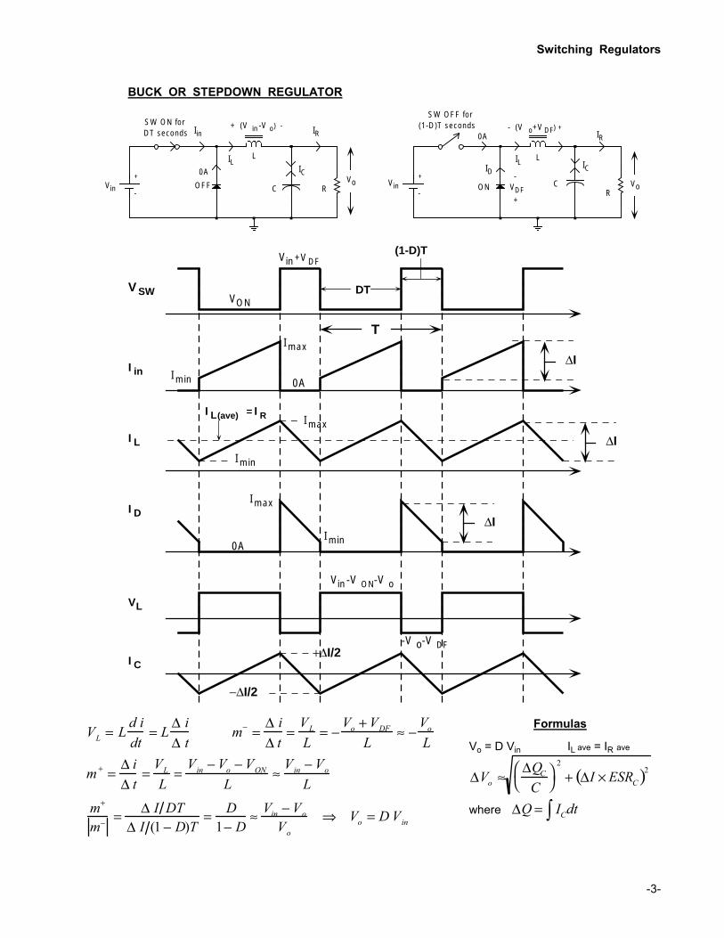
BUCK OR STEPDOWN REGULATOR
+
-Vin
SW ON forDT seconds
0A
OFF C
L
R
+ (V in-V o) -
Vo
IRIin
ICIL
+
-Vin
SW OFF for(1-D)T seconds
ON
L
R
- (V o+V DF) +
Vo
IR
ICIL
IDC
0A
-VDF+
I in
V SW
I L
VON
Vin+VDF
0A
Imax
Imin
Imax
Imin
∆I
∆I
I L(ave) = I R
I D
I C
0A
VL
-V o-V DF
Vin-V ON-V o
Imax
Imin
+∆I/2
−∆I/2
∆I
DT
(1-D)T
T
VL = Ld idt
= L∆ i∆ t
m− =∆ i∆ t
=VLL
= −Vo + VDFL
≈ −VoL
m + =∆ i∆ t
=VLL
=Vin − Vo − VON
L≈Vin − VoL
m+
m− = ∆ I DT∆ I (1 − D)T
= D1− D
≈ Vin − VoVo
⇒ Vo = DVin
Formulas
Vo = D Vin IL ave = IR ave
∆Vo ≈∆QCC
2
+ ∆I × ESRC( )2
where ∆Q = ICdt∫
Switching Regulators
-4-
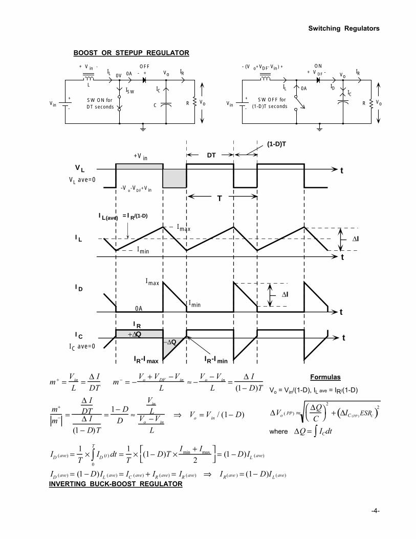
BOOST OR STEPUP REGULATOR
+
-
+
-
0A
VinVo
SW ON forDT seconds
SW OFF for(1-D)T seconds
+ V in -
C
L
R
IR
IC
IL 0V - +OFF
Vo
- (V o+VDF- Vin) +
Vin
+ V DF - VoIR
IDIC
IL 0AISW
VoR
ON
V L
I L
Imax
Imin
∆I
I L(ave) = I R/(1-D)
+V in
-V o-VDF+Vin
I D
I C
0A
Imax
Imin
∆I
DT
(1-D)T
T
I R
IR-I max IR-I min
+∆Q−∆Q
VL ave=0
IC ave=0
t
t
t
t
m + =VinL
=∆ IDT
m − = −Vo + VDF −Vin
L≈ −Vo − VinL
=∆ I
(1− D)T
m+
m− =
∆ IDT∆ I
(1− D)T
=1− DD
≈
VinL
Vo −VinL
⇒ Vo = Vin / (1− D)
Formulas
Vo = Vin/(1-D), IL ave = IR/(1-D)
∆Vo ( PP) ≈∆QC
2
+ ∆IC (PP )ESRC( )2
where ∆Q = ICdt∫
ID (ave) =1T
× ID (t )dt0
T
∫ =1T
× (1− D)T ×Imin + Imax
2
= (1 −D)IL (ave)
ID (ave) = (1−D)IL (ave) = IC (ave) + IR (ave) = IR (ave) ⇒ IR(ave ) = (1− D)IL (ave)
INVERTING BUCK-BOOST REGULATOR
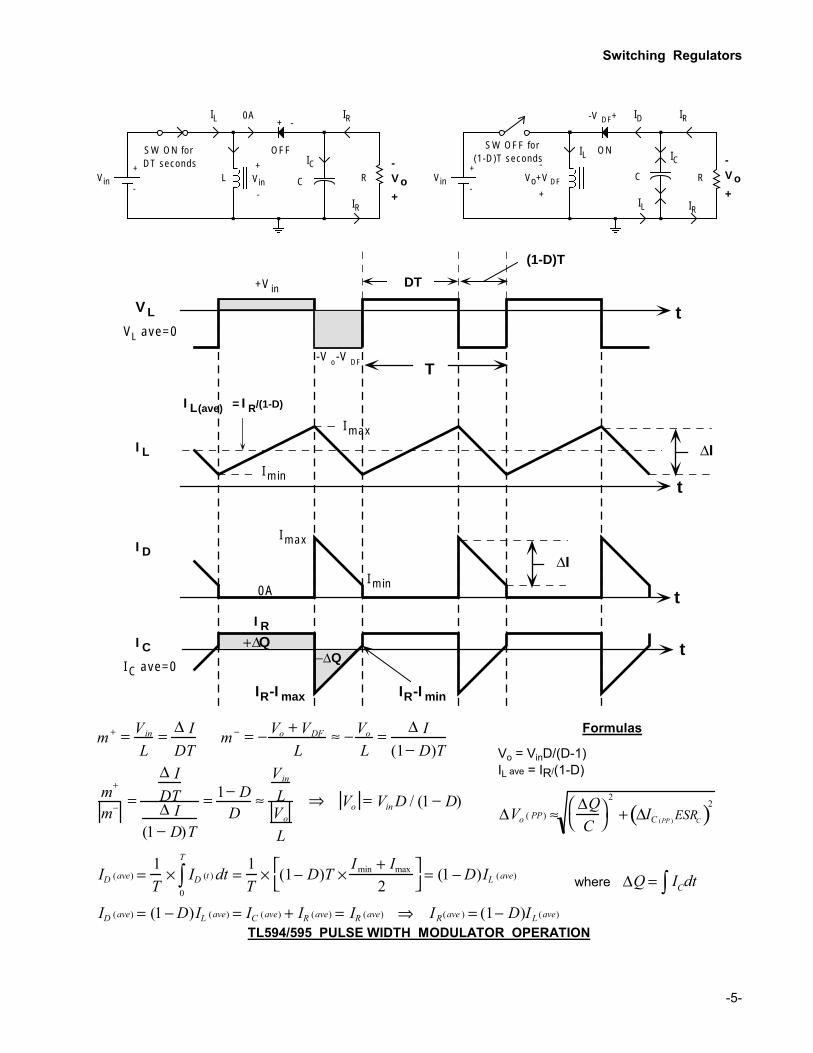
Switching Regulators
-5-
+
-
- +0A
+Vin-
-V o+
SW ON forDT seconds
C R
IR
ICOFF
Vin L
IL
IR
+
-
SW OFF for(1-D)T seconds
-V DF+
Vin
IRID
ICIL
R
-V o+
-Vo+V DF
+
ON
IL IR
C
V L
I L
Imax
Imin
∆I
I L(ave) = I R/(1-D)
+Vin
-V o-V DF
I D
I C
0A
Imax
Imin
∆I
DT
(1-D)T
T
I R
IR-I max IR-I min
+∆Q−∆Q
VL ave=0
IC ave=0
t
t
t
t
m + = VinL
= ∆ IDT
m − = − Vo + VDFL
≈ − VoL
= ∆ I(1− D)T
m+
m− =
∆ IDT∆ I
(1− D)T
= 1− DD
≈
VinLVoL
⇒ Vo = VinD / (1 − D)
Formulas
Vo = VinD/(D-1) IL ave = IR/(1-D)
∆Vo ( PP) ≈∆QC
2
+ ∆IC (PP )ESRC( )2
ID (ave) =1T
× ID (t )dt0
T
∫ =1T
× (1− D)T ×Imin + Imax
2
= (1 −D)IL (ave)
ID (ave) = (1−D)IL (ave) = IC (ave) + IR (ave) = IR (ave) ⇒ IR(ave ) = (1− D)IL (ave)
where ∆Q = ICdt∫
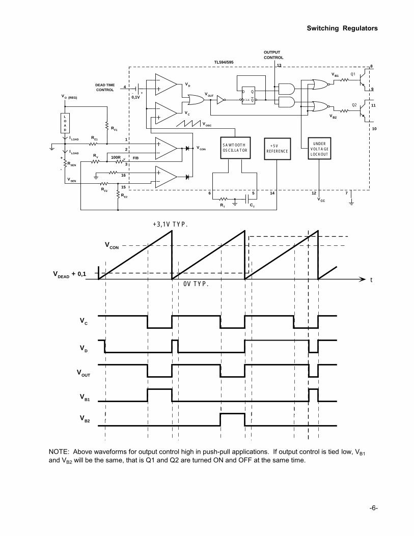
TL594/595 PULSE WIDTH MODULATOR OPERATION
Switching Regulators
-6-
+- D Q
Q
SAWTOOTHOSCILLATOR
+5VREFERENCE
UNDERVOLTAGELOCKOUT
Q1
Q2CLK
LOAD
VO (REG)
I LOAD
I LOAD
RF1
RE1
RE2
RF2
RSEN
+
-
RV 100R V
DEAD TIME CONTROL
OUTPUTCONTROL
VCCRT CT
VSEN
F/B
TL594/595
0,1V
4
1
2
16
15
3
6 5 14 12 7
8
9
10
11
13
VCON
VD
VC
VOUT
VOSC
VB1
VB2
0V TYP.
VCON
VDEAD + 0,1
+3,1V TYP.
t
VC
VD
VOUT
VB1
VB2
NOTE: Above waveforms for output control high in push-pull applications. If output control is tied low, VB1 and VB2 will be the same, that is Q1 and Q2 are turned ON and OFF at the same time.
Switching Regulators
-7-
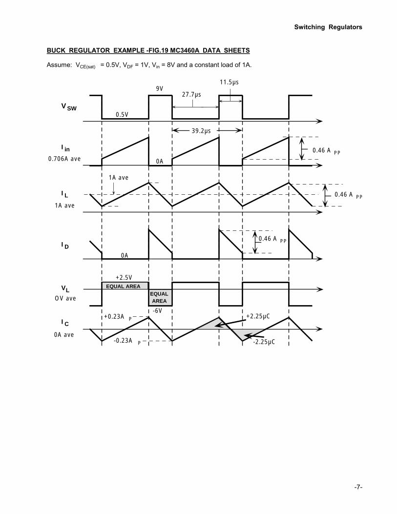
BUCK REGULATOR EXAMPLE -FIG.19 MC3460A DATA SHEETS Assume: VCE(sat) = 0.5V, VDF = 1V, Vin = 8V and a constant load of 1A.
I in
V SW
I L
0A
I D
I C
0A
VL
0.5V
9V
0.46 A PP
0.46 A PP
0.46 A PP
1A ave
27.7µs
11.5µs
39.2µs
+2.5V
-6V
-0.23A P
+0.23A P +2.25µC
OV ave
0A ave
0.706A ave
1A ave
EQUAL AREAEQUALAREA
-2.25µC
Switching Regulators
-8- 8
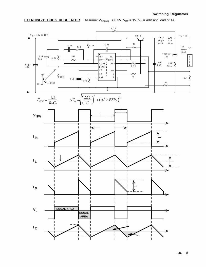
EXERCISE-1: BUCK REGULATOR Assume: VCE(sat) = 0.5V, VDF = 1V, Vin = 40V and load of 1A
LOAD
NI-1
INV-1
COMP
DEAD
CT
RT
GND
NI-2
INV-2
REF
Vcc
C
E
MC34060
Vin = +8V t o 40V Vo = 5V
1AFIXEDLOAD
10 nF47K
1M
47 µF63V
10 µF16V 4, 7K
3901 nF
47K
4, 7K
47
75
1000 µF10V
TIP32
MR850
10 nF
ESR50 m
150 µHat 2A
ESR50 m
0, 1
4, 7K
3, 3K
1000V 0,38V
+5V
FOSC ≈1,2RTCT
∆Vo ≈∆QCC
2
+ ∆I × ESRC( )2
I in
V SW
I L
I D
I C
VLEQUAL AREA
EQUALAREA
Switching Regulators
-9- 9
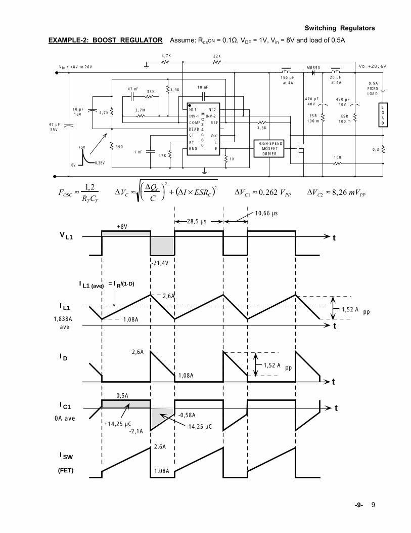
EXAMPLE-2: BOOST REGULATOR Assume: RdsON = 0.1Ω, VDF = 1V, Vin = 8V and load of 0,5A
0V 0,38V
+5V
LOAD
NI-1
INV-1
COMP
DEAD
CT
RT
GND
NI-2
INV-2
REF
Vcc
C
E
MC34060 HIGH-SPEED
MOSFETDRIVER
10 µF16V 4, 7K
3901 nF
47K
4, 7K
10 nF
3, 3K
100
Vin = +8V t o 26V
22K
3, 9K
47 µF35V
33K47 nF
2, 7M
0, 3
470 µF40V
ESR100 m
150 µHat 4A
470 µF40V
ESR100 m
0, 5AFIXEDLOAD
Vo = 28V
20 µHat 4A
MR850
1K
Vo=+28,4V
FOSC ≈ 1,2RTCT
∆VC ≈∆QCC
2
+ ∆I × ESRC( )2 ∆VC1 ≈ 0.262 VPP ∆VC2 ≈ 8,26 mVPP
V L1
I L1
I L1 (ave) = I R/(1-D)
I D
I C1
t
t
t
t
I SW
(FET)
0A ave
2.6A
1.08A
0,5A
-2,1A
2,6A
1,08A
2,6A
1,08A
1,52 A pp
1,52 A pp
1,838Aave
+8V
-21,4V
28,5 µs10,66 µs
-14,25 µC+14,25 µC-0,58A
Switching Regulators
-10- 10
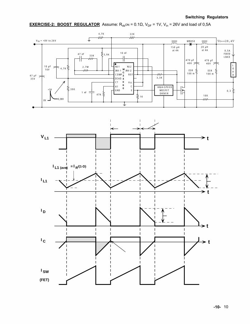
EXERCISE-2: BOOST REGULATOR Assume: RdsON = 0.1Ω, VDF = 1V, Vin = 26V and load of 0,5A
0V 0,38V
+5V
LOAD
NI-1
INV-1
COMP
DEAD
CT
RT
GND
NI-2
INV-2
REF
Vcc
C
E
MC34060 HIGH-SPEED
MOSFETDRIVER
10 µF16V 4, 7K
3901 nF
47K
4, 7K
10 nF
3, 3K
100
Vin = +8V t o 26V
22K
3, 9K
47 µF35V
33K47 nF
2, 7M
0, 3
470 µF40V
ESR100 m
150 µHat 4A
470 µF40V
ESR100 m
0, 5AFIXEDLOAD
Vo = 28V
20 µHat 4A
MR850
1K
Vo=+28,4V
V L1
I L1
I L1 (ave) = I R/(1-D)
I D
I C
t
t
t
t
I SW
(FET)
Switching Regulators
-11- 11
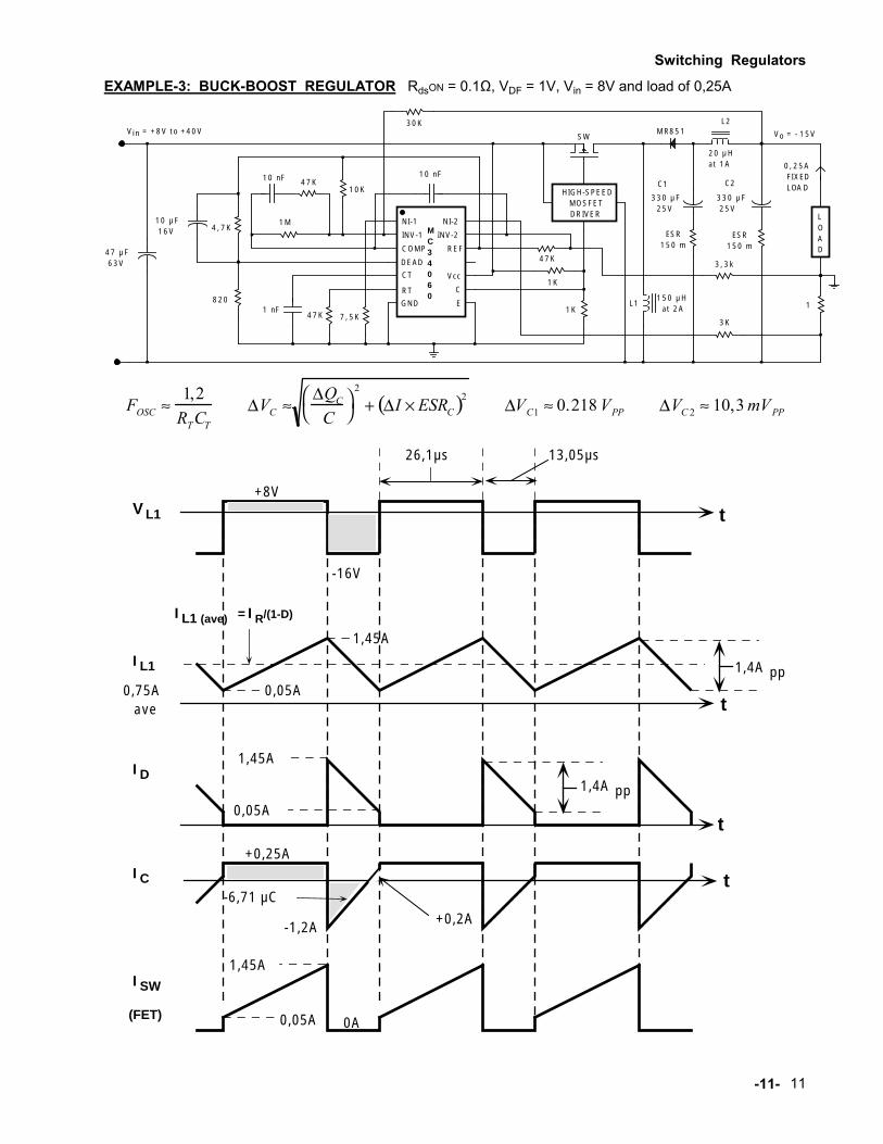
EXAMPLE-3: BUCK-BOOST REGULATOR RdsON = 0.1Ω, VDF = 1V, Vin = 8V and load of 0,25A
LOAD
NI-1
INV-1
COMP
DEAD
CT
RT
GND
NI-2
INV-2
REF
Vcc
C
E
MC34060
HIGH-SPEEDMOSFETDRIVER
L2
10 µF16V 4, 7K
1 nF47K
10 nF
Vin = +8V t o +40V Vo = - 15V
47 µF63V
8201
0, 25AFIXEDLOAD
47K3, 3k
3K
MR851
20 µHat 1A
330 µF25V
330 µF25V
ESR150 m
ESR150 m
150 µHat 2A
SW
L1
C1 C2
1K
1K
30K
10K
7, 5K
1M
10 nF 47K
FOSC ≈1,2RTCT
∆VC ≈∆QCC
2
+ ∆I × ESRC( )2 ∆VC1 ≈ 0.218VPP ∆VC 2 ≈ 10,3mVPP
V L1
I L1
I L1 (ave) = I R/(1-D)
I D
I C
t
t
t
t
I SW
(FET)0A
1,45A
0,05A
+0,2A
+0,25A
-1,2A
-6,71 µC
1,45A
0,05A
1,45A
0,05A0,75Aave
+8V
-16V
13,05µs26,1µs
1,4A pp
1,4A pp
Switching Regulators
-12- 12
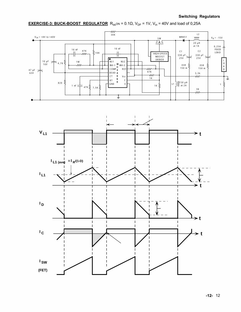
EXERCISE-3: BUCK-BOOST REGULATOR RdsON = 0.1Ω, VDF = 1V, Vin = 40V and load of 0,25A
LOAD
NI-1
INV-1
COMP
DEAD
CT
RT
GND
NI-2
INV-2
REF
Vcc
C
E
MC34060
HIGH-SPEEDMOSFETDRIVER
L2
10 µF16V 4, 7K
1 nF47K
10 nF
Vin = +8V t o +40V Vo = - 15V
47 µF63V
8201
0, 25AFIXEDLOAD
47K3, 3k
3K
MR851
20 µHat 1A
330 µF25V
330 µF25V
ESR150 m
ESR150 m
150 µHat 2A
SW
L1
C1 C2
1K
1K
30K
10K
7, 5K
1M
10 nF 47K
V L1
I L1
I L1 (ave) = I R/(1-D)
I D
I C
t
t
t
t
I SW
(FET)
-13- 13
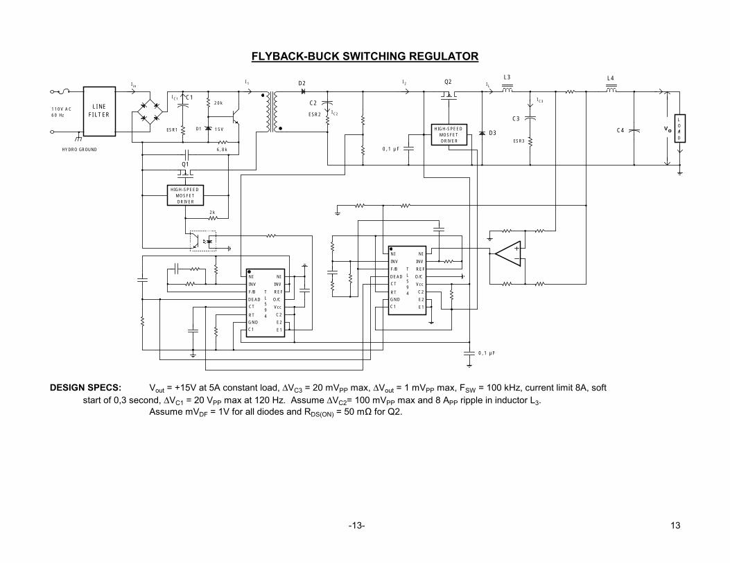
FLYBACK-BUCK SWITCHING REGULATOR
NI
INV
F/B
DEAD
CT
RT
GND
C1
NI
INV
REF
O/C
Vcc
C2
E2
E1
TL594
LOAD
NI
INV
F/B
DEAD
CT
RT
GND
C1
NI
INV
REF
O/C
Vcc
C2
E2
E1
TL594
HIGH-SPEEDMOSFETDRIVER
HIGH-SPEEDMOSFETDRIVER
Vo
I L
110V AC60 Hz
HYDRO GROUND
Q1
C1C2
D1
D2
D3
C3
L3 L4
C4
Q2II 1 2I in
I C3
ESR3
ESR1
LINEFILTER
15V
20k
6, 8k
2k
0 ,1 µ F
0 ,1 µ F
ESR2
I C1
I C2
DESIGN SPECS: Vout = +15V at 5A constant load, ∆VC3 = 20 mVPP max, ∆Vout = 1 mVPP max, FSW = 100 kHz, current limit 8A, soft start of 0,3 second, ∆VC1 = 20 VPP max at 120 Hz. Assume ∆VC2= 100 mVPP max and 8 APP ripple in inductor L3. Assume mVDF = 1V for all diodes and RDS(ON) = 50 mΩ for Q2.
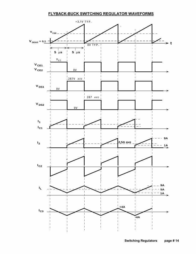
FLYBACK-BUCK SWITCHING REGULATOR WAVEFORMS
Switching Regulators page # 14
0V TYP.
VCON
V DEAD + 0,1
+3,1V TYP.
t
V CE1
V CE2 0V
Vcc
V DS1
V DS2
I1
I2
IL
IC3
IC2
IC1
287V AVE
0V
287 AVE
0V
2,5A ave9A
1A
9A
1A5A
+4A
-4A
5 µs 5 µs
Switching Regulators
-15-
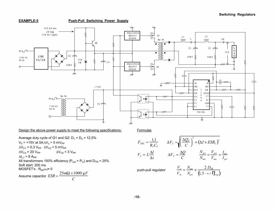
EXAMPLE-5 Push-Pull Switching Power Supply
NI
INV
F/B
DEAD
CT
RT
GND
C1
NI
INV
REF
O/C
Vcc
C2
E2
E1
TL594
HIGH-SPEEDMOSFETDRIVER
HIGH-SPEEDMOSFETDRIVER
C4
I L
110V AC60 Hz
110V AC60 Hz
Q1
Q2
Np: Ns
Np: Ns
LINEFILTER
100 kHz
1 5 V
5 AL1 L2
C1 C2
C3
1 5 V1 W
Q3
C5
+ 1 5 V
ESR1 ESR2
ESR3
1 4 3 ,6 V ave
2 0 Vpp1 2 0 Hz r i ppl e
LOAD
Design the above power supply to meet the following specifications: Average duty cycle of Q1 and Q2: D1 = D2 = 12,5% V0 = +15V at 5A ∆Vo = 5 mVPP ∆VC1 = 0,3 VPP ∆VC2 = 5 mVPP ∆VC3 = 20 VPP ∆VC5 < 3 VPP ∆IL1 = 8 APP All transformers 100% efficiency (Pout = Pin) and DTR = 25% Soft start: 200 ms MOSFET's : Rds(on)≈ 0
Assume capacitor ESR ≈25mΩ ×1000 µF
C
Formulas
FOSC ≈ 1,1RTCT
∆VC ≈∆QCC
2
+ ∆I × ESRC( )2
VL = L ∆I∆t
∆VC = ∆QC
NpriNsec
=VpriVsec
= IsecIpri
push-pull regulator VoVin
= NsecNpri
× 2 DTR1,5 − 0, 5ηreg( )
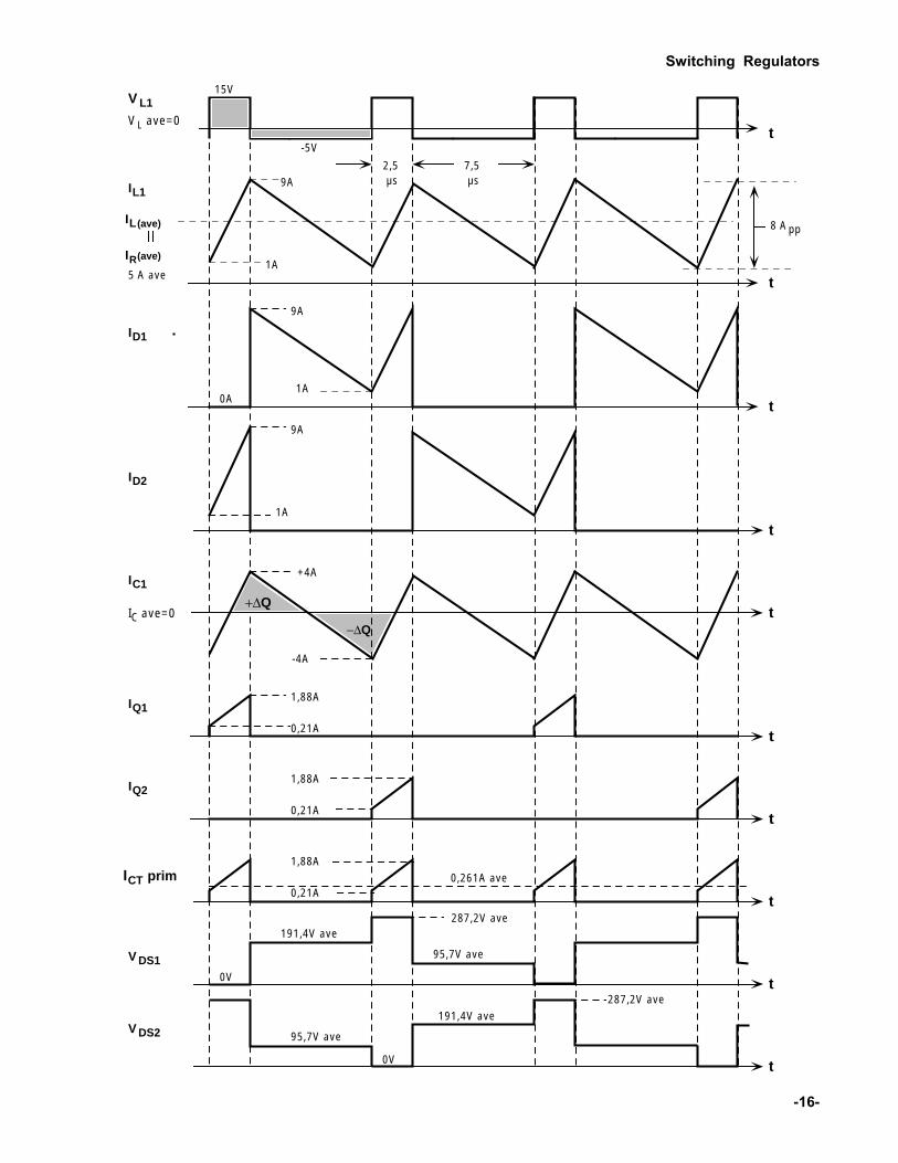
Switching Regulators
-16-
V L1
IL1
8 AppIL(ave)
IR(ave)
ID1
IC1
0A
VL ave=0
IC ave=0
t
t
t
ID2
+∆Q
−∆Q
IQ1
IQ2
t
t
V DS1
t
15V
-5V
5 A ave
9A
1A
9A
1A
9A
1A
+4A
-4A
7,5µs
2,5µs
t
t
V DS2
t
t
ICT prim
0,21A
1,88A
0,21A
1,88A
0,21A
1,88A
0V
191,4V ave287,2V ave
95,7V ave
191,4V ave
287,2V ave
95,7V ave
0V
0,261A ave
Switching Regulators
Switching Regulators page # 17
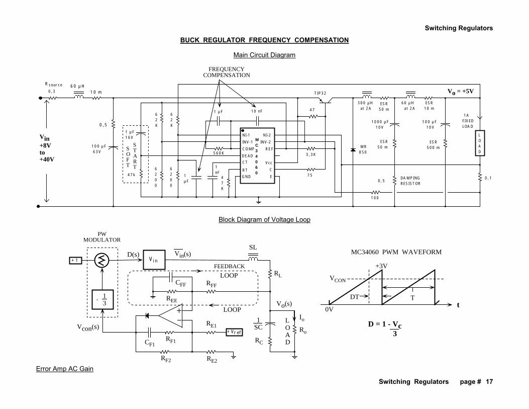
BUCK REGULATOR FREQUENCY COMPENSATION
Main Circuit Diagram
LOAD
NI-1
INV-1
COMP
DEAD
CT
RT
GND
NI-2
INV-2
REF
Vcc
C
E
MC34060
1AFIXEDLOAD
47
75
TIP32
MR850
10 nF
ESR50 m
0, 1
3, 3K
100
1 µF
1 µF16V
47k
100 µF10V
ESR500 m
300 µHat 2A
1000 µF10V
60 µHat 2A
ESR50 m
0, 5
ESR10 m
100 µF63V
0 ,5
6 0 µ H0, 3
Rsour ce
1 0 m
DAMPINGRESISTOR
560K
47K
1nF
6200
6200
62K
62K
1µF
Vin+8Vto+40V
Vo = +5V
SOFT
START
FREQUENCYCOMPENSATION
Block Diagram of Voltage Loop
+ Vr ef
-13
+ 1 Vi nD(s)
Vcon(s)
Vin(s)
Vo(s)
SL
RL
RC
Ro
1SC
PWMODULATOR
RFF
RE1
RE2RF2
RF1
REE
CF1
LOAD
Io
FEEDBACK
LOOP
LOOP
VCON
DT T
D = 1 - Vc3
t
MC34060 PWM WAVEFORM
+3V
0V
CFF
Error Amp AC Gain
Switching Regulators
Switching Regulators page # 18
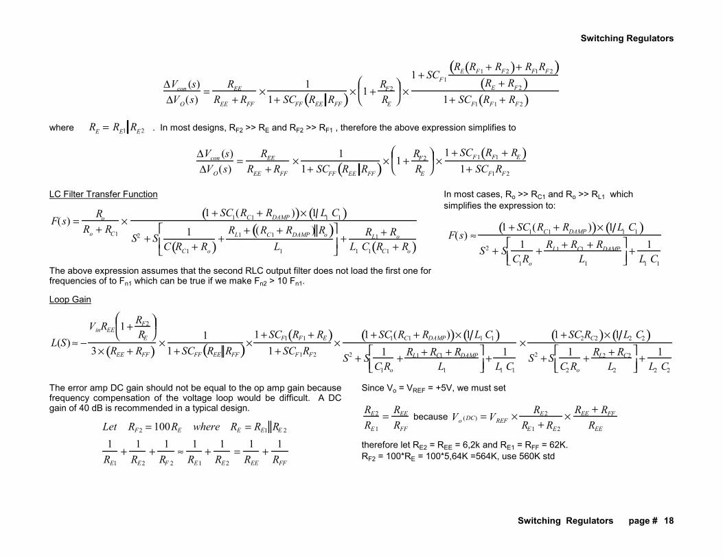
∆Vcon (s)∆VO(s)
=REE
REE + RFF×
11+ SCFF REE RFF( )× 1 +
RF2
RE
×
1 + SCF1
RE RF1 + RF2( )+ RF1RF2( )RE + RF2( )
1+ SCF1 RF1 + RF2( )
where RE = RE1 RE2 . In most designs, RF2 >> RE and RF2 >> RF1 , therefore the above expression simplifies to
∆Vcon (s)∆VO(s)
=REE
REE + RFF×
11+ SCFF REE RFF( )× 1 +
RF2
RE
×
1 + SCF1 RF1 + RE( )1+ SCF1RF2
LC Filter Transfer Function
F(s) =Ro
Ro + RC1
×1 + SC1(RC1 + RDAMP )( )× 1 L1 C1( )
S2 + S 1C RC1 + Ro( ) +
RL1 + (RC1 + RDAMP ) Ro( )L1
+
RL1 + RoL1 C1 RC1 + Ro( )
The above expression assumes that the second RLC output filter does not load the first one for frequencies of to Fn1 which can be true if we make Fn2 > 10 Fn1.
In most cases, Ro >> RC1 and Ro >> RL1 which simplifies the expression to:
F(s) ≈1 + SC1(RC1 + RDAMP )( )× 1 L1 C1( )
S2 + S 1C1Ro
+ RL1 + RC1 + RDAMPL1
+
1L1 C1
Loop Gain
L(S) ≈ −VinREE 1 + RF2
RE
3 × REE + RFF( ) ×1
1 + SCFF REE RFF( )×1 + SCF1 RF1 + RE( )
1 + SCF1RF2×
1 + SC1(RC1 + RDAMP)( )× 1 L1C1( )S2 + S 1
C1Ro+ RL1 + RC1 + RDAMP
L1
+
1L1 C1
×1 + SC2RC2( )× 1 L2 C2( )
S2 + S 1C2Ro
+ RL2 + RC2
L2
+
1L2 C2
The error amp DC gain should not be equal to the op amp gain because frequency compensation of the voltage loop would be difficult. A DC gain of 40 dB is recommended in a typical design.
Let RF2 = 100RE where RE = RE1 RE 2
1RE1
+1RE2
+1RF 2
≈1RE1
+1RE2
=1REE
+1RFF
Since Vo = VREF = +5V, we must set RE2
RE1
= REERFF
because Vo (DC) = VREF × RE2
RE1 + RE2
× REE+ RFFREE
therefore let RE2 = REE = 6,2k and RE1 = RFF = 62K. RF2 = 100*RE = 100*5,64K =564K, use 560K std
Switching Regulators
Switching Regulators page # 19
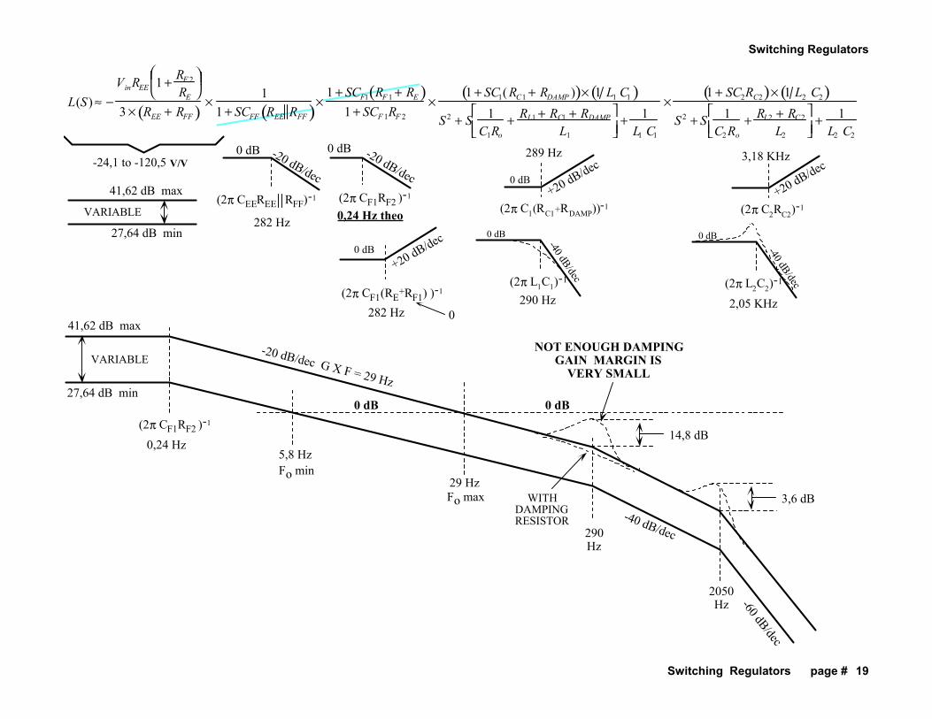
-24,1 to -120,5 V/V
27,64 dB min
41,62 dB max
VARIABLE
0 dB
(2π CEEREE RFF)-1
-20 dB/dec
(2π CF1RF2 )-1
0 dB -20 dB/dec
(2π CF1(RE+RF1) )-1
+20 dB/dec0 dB
282 Hz 0
(2π C1(RC1+RDAMP))-1
+20 dB/dec0 dB
(2π L1C1)-1
-40 dB/dec
0 dB
290 Hz
VARIABLE
(2π CF1RF2 )-1
290Hz
29 Hz
0,24 Hz
2050Hz
-40 dB/dec
-60 dB/dec
-20 dB/dec G X F = 29 Hz
0 dB
Fo max
Fo min
0 dB
NOT ENOUGH DAMPINGGAIN MARGIN IS
VERY SMALL27,64 dB min
41,62 dB max
WITHDAMPINGRESISTOR
14,8 dB
3,6 dB
5,8 Hz
(2π L2C2)-1
-40 dB/dec
0 dB
(2π C2RC2)-1
+20 dB/dec3,18 KHz
L(S) ≈ −VinREE 1 + RF 2
RE
3 × REE + RFF( ) × 11 + SCFF REE RFF( )×
1 + SCF1 RF 1 + RE( )1 + SCF 1RF 2
×1 + SC1(RC1 + RDAMP )( )× 1 L1 C1( )
S 2 + S 1C1Ro
+ RL1 + RC1 + RDAMPL1
+
1L1 C1
×1 + SC2RC2( )× 1 L2 C2( )
S 2 + S 1C2Ro
+ RL2 + RC2
L2
+
1L2 C2
2,05 KHz
289 Hz
282 Hz 0,24 Hz theo
Switching Regulators
Switching Regulators page # 20
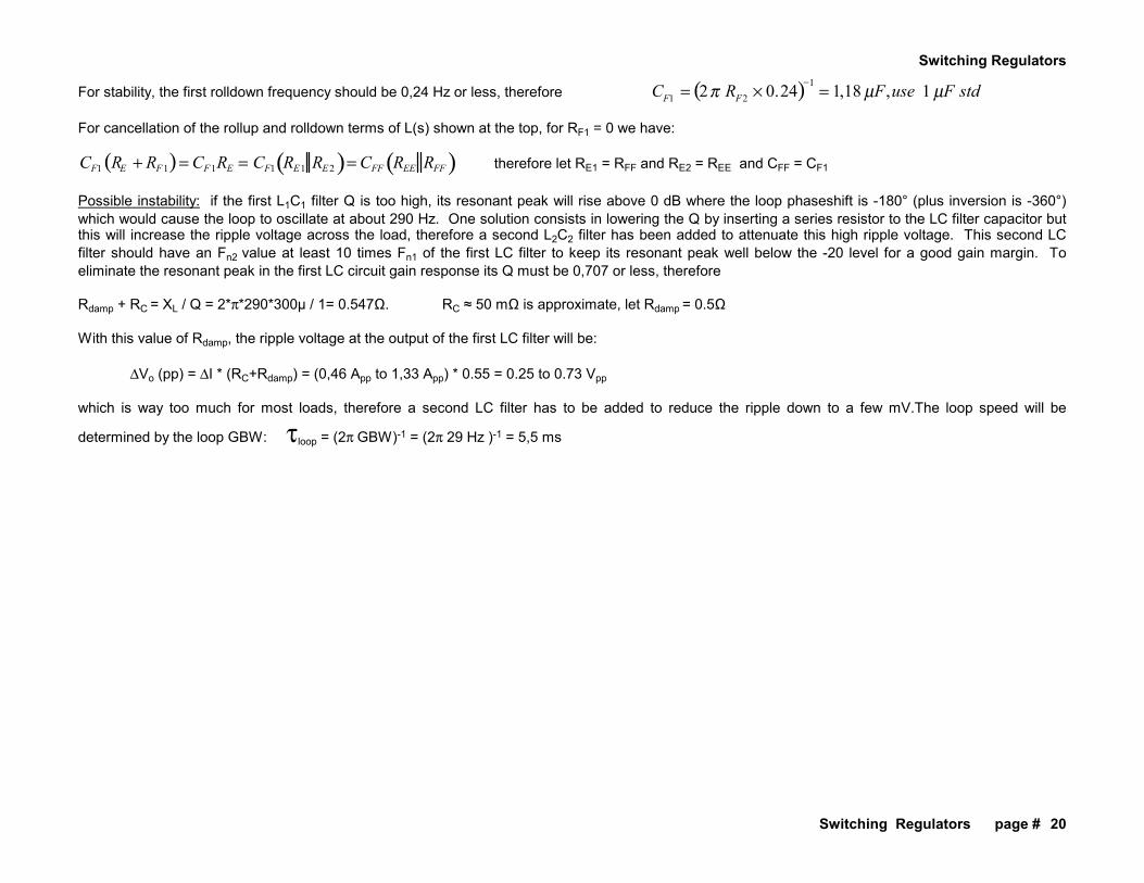
For stability, the first rolldown frequency should be 0,24 Hz or less, therefore CF1 = 2π RF2 × 0.24( )−1 = 1,18 µF,use 1 µF std For cancellation of the rollup and rolldown terms of L(s) shown at the top, for RF1 = 0 we have:
CF1 RE + RF1( )= CF1RE = CF1 RE1 RE2( )= CFF REE RFF( ) therefore let RE1 = RFF and RE2 = REE and CFF = CF1 Possible instability: if the first L1C1 filter Q is too high, its resonant peak will rise above 0 dB where the loop phaseshift is -180° (plus inversion is -360°) which would cause the loop to oscillate at about 290 Hz. One solution consists in lowering the Q by inserting a series resistor to the LC filter capacitor but this will increase the ripple voltage across the load, therefore a second L2C2 filter has been added to attenuate this high ripple voltage. This second LC filter should have an Fn2 value at least 10 times Fn1 of the first LC filter to keep its resonant peak well below the -20 level for a good gain margin. To eliminate the resonant peak in the first LC circuit gain response its Q must be 0,707 or less, therefore Rdamp + RC = XL / Q = 2*π*290*300µ / 1= 0.547Ω. RC ≈ 50 mΩ is approximate, let Rdamp = 0.5Ω With this value of Rdamp, the ripple voltage at the output of the first LC filter will be: ∆Vo (pp) = ∆I * (RC+Rdamp) = (0,46 App to 1,33 App) * 0.55 = 0.25 to 0.73 Vpp which is way too much for most loads, therefore a second LC filter has to be added to reduce the ripple down to a few mV.The loop speed will be
determined by the loop GBW: τloop = (2π GBW)-1 = (2π 29 Hz )-1 = 5,5 ms
Switching Regulators
Switching Regulators page # 21
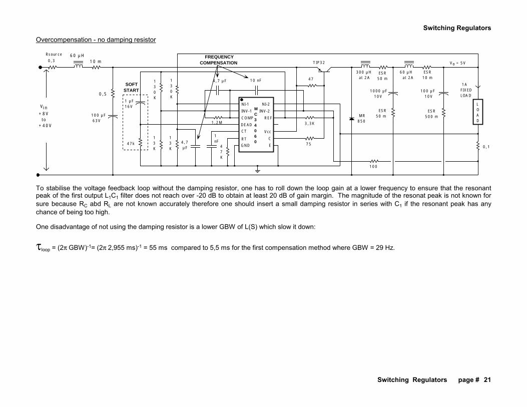
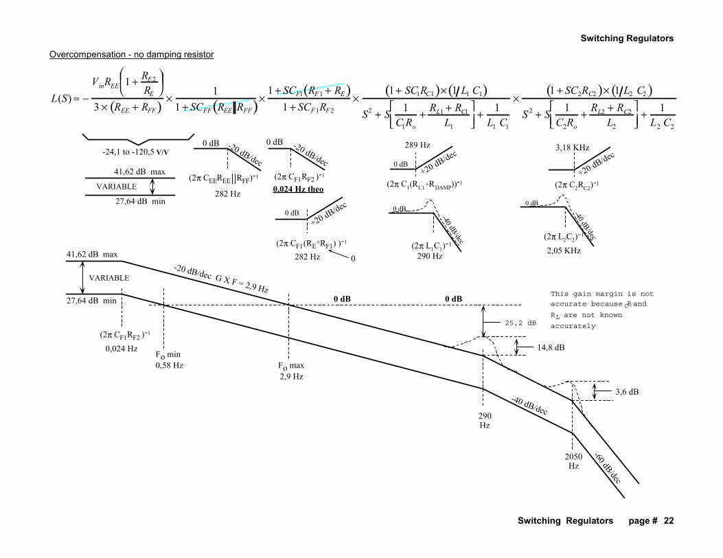
Overcompensation - no damping resistor
LOAD
NI-1
INV-1
COMP
DEAD
CT
RT
GND
NI-2
INV-2
REF
Vcc
C
E
MC34060
Vo = 5V
1AFIXEDLOAD
47
75
TIP32
MR850
10 nF
ESR50 m
0, 1
3, 3K
100
1 µF16V
47k
100 µF10V
ESR500 m
300 µHat 2A
1000 µF10V
60 µHat 2A
ESR50 m
ESR10 m
100 µF63V
0 ,5
Vi n+ 8 V
to+ 4 0 V
6 0 µ H0, 3
Rsour ce
1 0 m
47K
1nF
1, 2M
4, 7 µF
4, 7µF
130K
13K
130K
13K
SOFTSTART
FREQUENCYCOMPENSATION
To stabilise the voltage feedback loop without the damping resistor, one has to roll down the loop gain at a lower frequency to ensure that the resonant peak of the first output L1C1 filter does not reach over -20 dB to obtain at least 20 dB of gain margin. The magnitude of the resonat peak is not known for sure because RC abd RL are not known accurately therefore one should insert a small damping resistor in series with C1 if the resonant peak has any chance of being too high. One disadvantage of not using the damping resistor is a lower GBW of L(S) which slow it down:
τloop = (2π GBW)-1= (2π 2,955 ms)-1 = 55 ms compared to 5,5 ms for the first compensation method where GBW = 29 Hz.
Switching Regulators
Switching Regulators page # 22
Overcompensation - no damping resistor
-24,1 to -120,5 V/V
27,64 dB min
41,62 dB max
VARIABLE
0 dB
(2π CEEREE RFF)-1
-20 dB/dec
(2π CF1RF2 )-1
0 dB -20 dB/dec
(2π CF1(RE+RF1) )-1
+20 dB/dec0 dB
282 Hz 0
(2π C1(RC1+RDAMP))-1
+20 dB/dec0 dB
(2π L1C1)-1
290 Hz
-40 dB/dec
0 dB
VARIABLE
(2π CF1RF2 )-1
290Hz
2,9 Hz
0,024 Hz
2050Hz
-40 dB/dec
-60 dB/dec
-20 dB/dec G X F = 2,9 Hz0 dB
Fo maxFo min
0 dB27,64 dB min
41,62 dB max
14,8 dB
3,6 dB
0,58 Hz
25,2 dB
This gain margin is not
accurate because RC and
RL are not known
accurately
(2π L2C2)-1
-40 dB/dec
0 dB
(2π C2RC2)-1+20 dB/dec
3,18 KHz
2,05 KHz
289 Hz
282 Hz 0,024 Hz theo
L(S) ≈ −VinREE 1 + RF2
RE
3 × REE + RFF( ) ×1
1 + SCFF REE RFF( )×1 + SCF1 RF1 + RE( )
1 + SCF1RF2×
1+ SC1RC1( )× 1 L1 C1( )S2 + S 1
C1Ro+ RL1 + RC1
L1
+
1L1 C1
×1 + SC2RC2( )× 1 L2 C2( )
S 2 + S 1C2Ro
+ RL2 + RC2
L2
+
1L2 C2
Switching Regulators
Switching Regulators page # 23
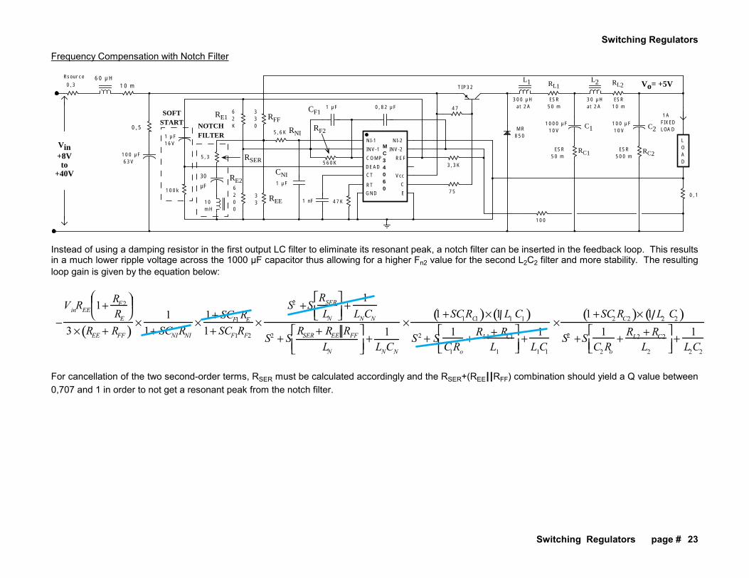
Frequency Compensation with Notch Filter
LOAD
NI-1
INV-1
COMP
DEAD
CT
RT
GND
NI-2
INV-2
REF
Vcc
C
E
MC34060
1AFIXEDLOAD
1 nF 47K
47
75
TIP32
MR850
0, 1
3, 3K
100
1 µF
1 µF16V
ESR500 m
100 µF10V
0, 82 µF
1000 µF10V
ESR50 m
ESR10 m
300 µHat 2A
100 µF63V
0 ,5
10mH
5, 3
100k
330
6 0 µ H0, 3
Rsour ce
ESR50 m
1 0 m
560K
30 µHat 2A
6200
62K
5, 6K
1 µF
33
Vo= +5V
Vin+8Vto
+40V
SOFTSTART
30
µF
NOTCHFILTER
L1 L2
C1 C2
RL1 RL2
RC2RC1
RFF
REE
RE1
RE2
RF2
CF1
RSER
RNI
CNI
Instead of using a damping resistor in the first output LC filter to eliminate its resonant peak, a notch filter can be inserted in the feedback loop. This results in a much lower ripple voltage across the 1000 µF capacitor thus allowing for a higher Fn2 value for the second L2C2 filter and more stability. The resulting loop gain is given by the equation below:
−VinREE 1+ RF2
RE
3 × REE + RFF( ) ×1
1+ SCNIRNI×
1+ SCF1RE1+ SCF1RF2
×S2 +S
RSERLN
+
1LNCN
S2 + SRSER+ REE RFF
LN
+1LNCN
×1 +SC1RC1( )× 1 L1 C1( )
S 2 + S 1C1Ro
+ RL1 + RC1
L1
+
1L1C1
×1 +SC2RC2( )× 1 L2 C2( )
S2 +S 1C2Ro
+ RL2 + RC2
L2
+
1L2C2
For cancellation of the two second-order terms, RSER must be calculated accordingly and the RSER+(REEIIRFF) combination should yield a Q value between 0,707 and 1 in order to not get a resonant peak from the notch filter.
Switching Regulators
Switching Regulators page # 24
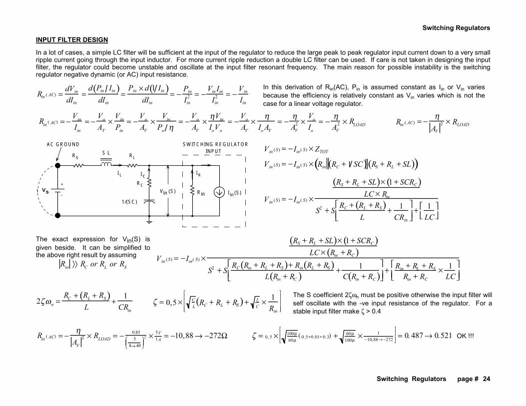
INPUT FILTER DESIGN In a lot of cases, a simple LC filter will be sufficient at the input of the regulator to reduce the large peak to peak regulator input current down to a very small ripple current going through the input inductor. For more current ripple reduction a double LC filter can be used. If care is not taken in designing the input filter, the regulator could become unstable and oscillate at the input filter resonant frequency. The main reason for possible instability is the switching regulator negative dynamic (or AC) input resistance.
Rin ( AC) =dVindIin
=d Pin Iin( )dIin
=Pin × d 1 Iin( )
dIin= −
PinIin
2 = −Vin IinIin
2 = −VinIin
In this derivation of Rin(AC), Pin is assumed constant as Iin or Vin varies because the efficiency is relatively constant as Vin varies which is not the case for a linear voltage regulator.
Rin ( AC) = −VinIin
= −VoAV
×VinPin
= −VoAV
×VinPo η
= −VoAV
×ηVinIoVo
= −VoAV
×ηIoAV
= −ηAV
2 ×VoIo
= −ηAV
2 × RLOAD Rin ( AC) = −ηAV
2 × RLOAD
+
-
Rs RL
RC
Rin
1/(SC)
S L
Vs I in(S)
SWITCHING REGULATORINPUT
Vin (S)
I L Ic IR
AC GROUND
Vin (S) = − Iin( S) × ZTOT
Vin (S) = − Iin( S) × Rin RC + 1 SC( ) RS + RL + SL( )( )
Vin (S) = − Iin( S) ×
RS + RL + SL( )× 1 + SCRC( )LC × Rin
S2 + S RC+ RL + RS( )L
+ 1CRin
+1LC
The exact expression for Vin(S) is given beside. It can be simplified to the above right result by assuming
Rin ⟩⟩ RC or RL or RS
Vin (S) = − Iin( S) ×
RS + RL + SL( )× 1 + SCRC( )LC × Rin + RC( )
S2 + S RC Rin+ RL + RS( )+ Rin RL + RS( )L Rin + RC( ) + 1
C Rin + RC( )
+Rin + RL + RSRin + RC
× 1LC
2ζωn =RC + RL + RS( )
L+
1CRin
ζ = 0,5 × CL RC + RL + RS( )+ L
C× 1Rin
The S coefficient 2ζωn must be positive otherwise the input filter will self oscillate with the -ve input resistance of the regulator. For a stable input filter make ζ > 0.4
Rin ( AC) = −ηAV
2 × RLOAD = − 0.855
8→ 40
2 × 5V1A = −10,88 → −272Ω ζ = 0, 5 × 100µ
60 µ0.5+0.01+ 0.3( ) + 60 µ
100µ× 1
−10,88→ −272
= 0. 487 → 0.521 OK !!!
Switching Regulators
Switching Regulators page # 25
Design criteria for input filter 1. Make Fn (in) > 7 * Fn (out) of the first output LC filter to avoid interaction between the two filters 2. Select Lin formaximum ripple current in source:
∆Iin (PP) = 1L VL (AC ) dt
0
DT
∫ = 1L VL (AC ) dtDT
T
∫ = RCL IC dt
0
DT
∫ ⟨ ∆Iin max in DC source
3. Select appropriate L/C ratio to make input filter damping high enough or add a damping resistor where appropriate.
ζ = 0,5 × CLRC + RL + RS( )+ L
C×
1Rin
⟩ 0,4 for a stable input filter where Rin ( AC) = −
ηAV
2 × RLOAD