Embed Size (px)
Citation preview
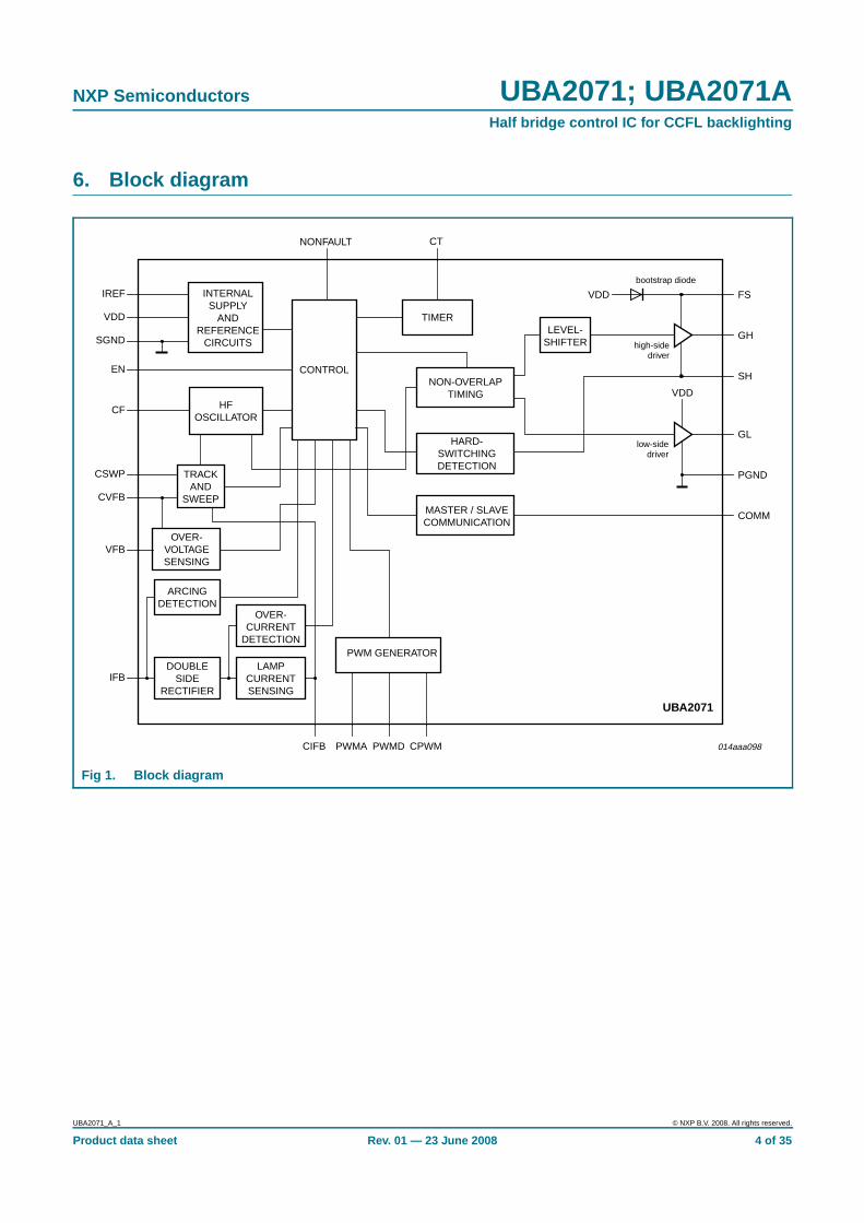
1. General description
The UBA2071 and UBA2071A are high voltage ICs intended to drive Cold CathodeFluorescent Lamps (CCFLs) or External Electrode Fluorescent Lamps (EEFLs) forbacklighting applications. They can drive a half bridge circuit made up of two NMOSFETswith a supply voltage of up to 550 V, so the inverter can be supplied directly from a 400 VPFC bus.
The UBA2071 and UBA2071A contain a controller, a level shifter, a bootstrap diode anddrivers for the external half bridge power switches. It also contains a low frequency PWMgenerator, which can be used to control the brightness level of the lamps, using an analogbrightness/dimming control voltage. PWM dimming can also be realized, using a digitalPWM input signal. PWM dimming can be synchronized with other ICs. The lamp current iscontrolled by means of a true zero voltage switching resonant control principle, ensuringlowest possible switch losses in the half bridge power structure.
The UBA2071 is designed to be supplied by a ∆V/∆t supply from the half bridge circuit thatit drives. The IC itself needs little current and if the IC is off, a clamp protects the supplyvoltage from getting too high.
The UBA2071A is designed to be supplied by a fixed 12 V supply. It has a lower supplystart voltage and no supply clamp.
2. Features
n Suitable for operating in a very wide inverter supply voltage range (up to 550 V DC).
n Integrated level shifter.
n Integrated bootstrap diode.
n Lamp current control by means of a true zero voltage switching resonant controlprinciple.
n Sample & Hold circuit, maintaining current control value during PWM lamp-offsituation.
n Separately definable time constants for current control loop and PWM dimmingattack/decay setting.
n Overvoltage control.
n Overcurrent protection.
n Ignition failure detection.
n Hard switching control.
n Arcing detection.
n Open/short pin protections on feedback pins.
n Integrated, programmable fault timer.
UBA2071; UBA2071AHalf bridge control IC for CCFL backlightingRev. 01 — 23 June 2008 Product data sheet
NXP Semiconductors UBA2071; UBA2071AHalf bridge control IC for CCFL backlighting
n Bidirectional pin acting both as fault signaling output and input, allowing external faultinterfacing to operate via the integrated fault timer.
n Brightness level adjustment through PWM dimming.
n Integrated PWM generator.
n Power-down mode.
n Communication pin for master / slave operation.
n DC blocking capacitor pre-charging sequence.
n Supply clamp (UBA2071 only).
3. Applications
n LCD-backlighting, including LCD-TV and LCD-monitor applications. The IC is intendedto drive and control a half bridge inverter with resonant load circuit for CCFLs, but canalso drive an array of External Electrode Fluorescent Lamps (EEFLs).
4. Quick reference data
Table 1. Quick reference data.Tamb = 25 °C; VVDD = 12 V; RIREF = 33 kΩ; VEN = VVDD and CPWM connected to a capacitor, unlessotherwise specified. All voltages are measured with respect to signal ground (SGND, pin 10). SGNDand PGND connected together. Currents are positive when flowing into the IC.
Symbol Parameter Conditions Min Typ Max Unit
VSH voltage on pin SH - - 550 V
VVDD voltage on pin VDD - - 14 V
IVDD current on pin VDD EN pin grounded;VVDD = 14.0 V;UBA2071AT andUBA2071ATS
- - 0.22 mA
oscillating at fsw(min);CCF = 100 pF
1.2 1.5 1.8 mA
disabled;VVDD = 11 V
- 0.16 - mA
oscillating;CF = 100 pF;GL and GH open
- 1.5 - mA
CCF = 100 pF;VPWMD = H;VCSWP = 0 V
1.0 1.2 1.4 mA
fsw(min) minimum switchingfrequency
CCF = 100 pF [1]
[2]10 - 100 kHz
[1]
[2]38 40 42 kHz
fsw(max)/fsw(min) maximum switchingfrequency tominimum switchingfrequency ratio
2.2 2.4 2.6 kHz
Vref(creg) current regulationreference voltage
1.20 1.26 1.32 V
UBA2071_A_1 © NXP B.V. 2008. All rights reserved.
Product data sheet Rev. 01 — 23 June 2008 2 of 35
NXP Semiconductors UBA2071; UBA2071AHalf bridge control IC for CCFL backlighting
[1] Given frequency is switching frequency of GL and GH. Sawtooth frequency on CF pin is twice as high.
[2] Can be set by external capacitor
[3] PWMD is active low: A low level on the PWMD pin corresponds with lamps-on. Example: δPWM = 20 %means PWMD is during 20 % of each cycle low and the lamps are 20 % of the time on, resulting in a lightoutput of 20 %.
5. Ordering information
Vth(ov)(VFB) overvoltagethreshold voltage onpin VFB
2.40 2.50 2.60 V
tto(fault) fault time-out time CCT = 100 nF 0.85 1.00 1.15 s
Isource(drv) driver sourcecurrent
VGL, VGH = 4 V;VVDD = VFS = 12 V
−105 −90 −75 mA
Rsink(drv) driver sinkresistance
VGL, VGH = 2 V;VVDD = VFS = 12 V
13.5 16.0 18.5 Ω
fPWM PWM frequency [1] 75 - 1000 Hz
δPWMD duty cycle on pinPWMD
[3] 12 - 100 %
Table 1. Quick reference data.Tamb = 25 °C; VVDD = 12 V; RIREF = 33 kΩ; VEN = VVDD and CPWM connected to a capacitor, unlessotherwise specified. All voltages are measured with respect to signal ground (SGND, pin 10). SGNDand PGND connected together. Currents are positive when flowing into the IC.
Symbol Parameter Conditions Min Typ Max Unit
Table 2. Ordering information
Type number Package
Name Description Version
UBA2071T SO24 plastic small outline package; 24 leads; body width 7.5 mm SOT137-1
UBA2071AT SO24 plastic small outline package; 24 leads; body width 7.5 mm SOT137-1
UBA2071TS SSOP24 plastic shrink small outline package; 24 leads;body width 5.3 mm
SOT340-1
UBA2071ATS SSOP24 plastic shrink small outline package; 24 leads;body width 5.3 mm
SOT340-1
UBA2071_A_1 © NXP B.V. 2008. All rights reserved.
Product data sheet Rev. 01 — 23 June 2008 3 of 35
NXP Semiconductors UBA2071; UBA2071AHalf bridge control IC for CCFL backlighting
6. Block diagram
Fig 1. Block diagram
ARCINGDETECTION
DOUBLESIDE
RECTIFIER
HARD-SWITCHINGDETECTION
MASTER / SLAVECOMMUNICATION
NON-OVERLAPTIMING
PWM GENERATORLAMP
CURRENTSENSING
OVER-CURRENT
DETECTION
OVER-VOLTAGESENSING
TRACKAND
SWEEP
INTERNALSUPPLY
ANDREFERENCE
CIRCUITSLEVEL-
SHIFTER
TIMER
HFOSCILLATOR
CONTROL
IREF
VDD
EN
CF
CSWP
CVFB
VFB
IFB
CIFB PWMA PWMD CPWM
FS
GH
SH
GL
PGND
COMM
VDD
bootstrap diode
VDD
low-sidedriver
high-sidedriver
UBA2071
SGND
CTNONFAULT
014aaa098
UBA2071_A_1 © NXP B.V. 2008. All rights reserved.
Product data sheet Rev. 01 — 23 June 2008 4 of 35
NXP Semiconductors UBA2071; UBA2071AHalf bridge control IC for CCFL backlighting
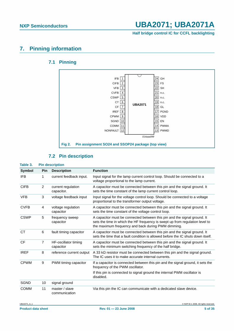
7. Pinning information
7.1 Pinning
7.2 Pin description
Fig 2. Pin assignment SO24 and SSOP24 package (top view)
UBA2071
IFB GH
CIFB FS
VFB SH
CVFB n.c.
CSWP n.c.
CT n.c.
CF GL
IREF PGND
CPWM VDD
SGND EN
COMM PWMA
NONFAULT PWMD
014aaa099
1
2
3
4
5
6
7
8
9
10
11
12
14
13
16
15
18
17
20
19
22
21
24
23
Table 3. Pin description
Symbol Pin Description Function
IFB 1 current feedback input. Input signal for the lamp current control loop. Should be connected to avoltage proportional to the lamp current.
CIFB 2 current regulationcapacitor.
A capacitor must be connected between this pin and the signal ground. Itsets the time constant of the lamp current control loop.
VFB 3 voltage feedback input Input signal for the voltage control loop. Should be connected to a voltageproportional to the transformer output voltage.
CVFB 4 voltage regulationcapacitor
A capacitor must be connected between this pin and the signal ground. Itsets the time constant of the voltage control loop.
CSWP 5 frequency sweepcapacitor
A capacitor must be connected between this pin and the signal ground. Itsets the time in which the HF frequency is swept up from regulation level tothe maximum frequency and back during PWM dimming.
CT 6 fault timing capacitor A capacitor must be connected between this pin and the signal ground. Itsets the time that a fault condition is allowed before the IC shuts down itself.
CF 7 HF-oscillator timingcapacitor
A capacitor must be connected between this pin and the signal ground. Itsets the minimum switching frequency of the half bridge.
IREF 8 reference current output A 33 kΩ resistor must be connected between this pin and the signal ground.The IC uses it to make accurate internal currents.
CPWM 9 PWM timing capacitor If a capacitor is connected between this pin and the signal ground, it sets thefrequency of the PWM oscillator.
If this pin is connected to signal ground the internal PWM oscillator isdisabled.
SGND 10 signal ground
COMM 11 master / slavecommunication
Via this pin the IC can communicate with a dedicated slave device.
UBA2071_A_1 © NXP B.V. 2008. All rights reserved.
Product data sheet Rev. 01 — 23 June 2008 5 of 35
NXP Semiconductors UBA2071; UBA2071AHalf bridge control IC for CCFL backlighting
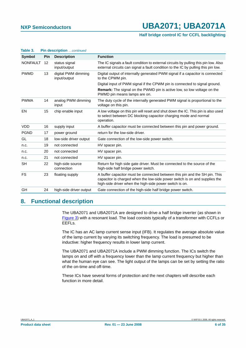
8. Functional description
The UBA2071 and UBA2071A are designed to drive a half bridge inverter (as shown inFigure 3) with a resonant load. The load consists typically of a transformer with CCFLs orEEFLs.
The IC has an AC lamp current sense input (IFB). It regulates the average absolute valueof the lamp current by varying its switching frequency. The load is presumed to beinductive: higher frequency results in lower lamp current.
The UBA2071 and UBA2071A include a PWM dimming function. The ICs switch thelamps on and off with a frequency lower than the lamp current frequency but higher thanwhat the human eye can see. The light output of the lamps can be set by setting the ratioof the on-time and off-time.
These ICs have several forms of protection and the next chapters will describe eachfunction in more detail.
NONFAULT 12 status signalinput/output
The IC signals a fault condition to external circuits by pulling this pin low. Alsoexternal circuits can signal a fault condition to the IC by pulling this pin low.
PWMD 13 digital PWM dimminginput/output
Digital output of internally generated PWM signal if a capacitor is connectedto the CPWM pin.
Digital input of PWM signal if the CPWM pin is connected to signal ground.
Remark: The signal on the PWMD pin is active low, so low voltage on thePWMD pin means lamps are on.
PWMA 14 analog PWM dimminginput
The duty cycle of the internally generated PWM signal is proportional to thevoltage on this pin.
EN 15 chip enable input A low voltage on this pin will reset and shut down the IC. This pin is also usedto select between DC blocking capacitor charging mode and normaloperation.
VDD 16 supply input A buffer capacitor must be connected between this pin and power ground.
PGND 17 power ground return for the low-side driver.
GL 18 low-side driver output Gate connection of the low-side power switch.
n.c. 19 not connected HV spacer pin.
n.c. 20 not connected HV spacer pin.
n.c. 21 not connected HV spacer pin.
SH 22 high-side sourceconnection
Return for high side gate driver. Must be connected to the source of thehigh-side half bridge power switch.
FS 23 floating supply A buffer capacitor must be connected between this pin and the SH pin. Thiscapacitor is charged when the low-side power switch is on and supplies thehigh-side driver when the high-side power switch is on.
GH 24 high-side driver output Gate connection of the high-side half bridge power switch.
Table 3. Pin description …continued
Symbol Pin Description Function
UBA2071_A_1 © NXP B.V. 2008. All rights reserved.
Product data sheet Rev. 01 — 23 June 2008 6 of 35
NXP Semiconductors UBA2071; UBA2071AHalf bridge control IC for CCFL backlighting
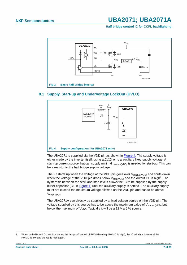
8.1 Supply, Start-up and UnderVoltage LockOut (UVLO)
The UBA2071 is supplied via the VDD pin as shown in Figure 4. The supply voltage iseither made by the inverter itself, using a ∆V/∆t or is a auxiliary fixed supply voltage. Astart-up current source that can supply minimal Istartup(VDD) is needed for start-up. This canbe a resistor to the half bridge supply voltage.
The IC starts up when the voltage at the VDD pin goes over Vstartup(VDD) and shuts downwhen the voltage at the VDD pin drops below Vstop(VDD) and the output GL is high1. Thehysteresis between the start and stop levels allows the IC to be supplied by the supplybuffer capacitor (C1 in Figure 4) until the auxiliary supply is settled. The auxiliary supplymust not exceed the maximum voltage allowed on the VDD pin and has to be aboveVstop(VDD).
The UBA2071A can directly be supplied by a fixed voltage source on the VDD pin. Thevoltage supplied by this source has to be above the maximum value of Vstartup(VDD) butbelow the maximum of VVDD. Typically it will be a 12 V ± 5 % source.
Fig 3. Basic half bridge inverter
LOAD
VHV
0.5 VHVVHB
GL
SH
GH
FS
VDD
PGND
UBA2071
014aaa100
CFS QHS
QLS Cblock
Fig 4. Supply configuration (for UBA2071 only)
1. When both GH and GL are low, during the lamps-off period of PWM dimming (PWMD is high), the IC will shut down until thePWMD is low and the GL is high again.
UBA2071
VDD
startup
current
AUXILARYSUPPLY
C1
014aaa101
UBA2071_A_1 © NXP B.V. 2008. All rights reserved.
Product data sheet Rev. 01 — 23 June 2008 7 of 35
NXP Semiconductors UBA2071; UBA2071AHalf bridge control IC for CCFL backlighting
8.2 VDD clampWhen the UBA2071 is disabled (EN pin low) or in the stop state, the VDD clamp isactivated. The VDD clamp is an internal active zener limiting the voltage to Vclamp(VDD). Itprevents the start-up current source from charging the VDD buffer capacitor to too high avoltage.
The maximum current that is allowed to be delivered by the start-up current source isdetermined by the clamp voltage as stated in Table 6 and the maximum allowed VDDvoltage as stated in Table 4.
The UBA2071A has no VDD clamp.
8.3 EnableThe UBA2071 or UBA2071A can be activated or set to standby via the EN pin. If thevoltage on the EN pin is below Vth(L)(EN), the IC will stop oscillating at the next GL highstate2, and most parts of the internal circuits will shut down. When the EN pin is left open,it is pulled low by an internal bias current of Ibias(EN).
When the voltage on the EN pin comes above Vth(H)1(EN), the IC will start up inDC blocking capacitor charging mode (see Section 8.8). When the voltage on the EN pingoes over Vth(H)2(EN), the IC will start with the initial ignition frequency sweep (seeSection 8.8) and subsequently go to normal operation mode again.
8.4 The oscillatorThe UBA2071 and UBA2071A have an internal voltage controlled sawtooth oscillator, seeFigure 5. Its frequency inverses in proportion to the capacitor connected to the CF pin.The IC switches GL on and GH off during one oscillator period and GL off and GH onduring the next oscillator period. This results in a half bridge voltage with a frequency(called the switching frequency fsw from here on) of half the oscillator frequency and with aduty cycle of exactly 50 %.
The oscillator frequency is controlled by changing the charge current at the CF pin. Bychanging the frequency the lamp current is controlled. It is also used to limit thetransformer output voltage and for gradually switching the lamps on and off during PWMdimming.
2. When both GH and GL are low during the lamps off period of PWM dimming (so PWMD is high), the IC will wait with entering thestandby state until PWMD becomes low again and GL can be made high.
UBA2071_A_1 © NXP B.V. 2008. All rights reserved.
Product data sheet Rev. 01 — 23 June 2008 8 of 35
NXP Semiconductors UBA2071; UBA2071AHalf bridge control IC for CCFL backlighting
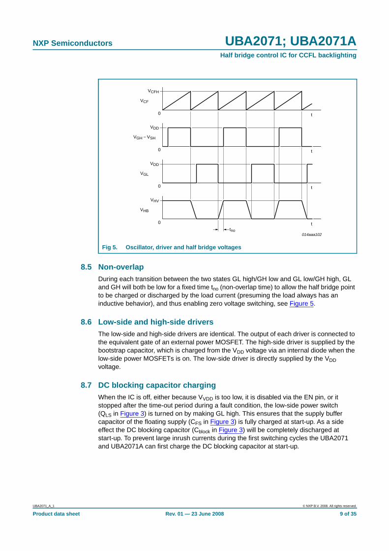
8.5 Non-overlapDuring each transition between the two states GL high/GH low and GL low/GH high, GLand GH will both be low for a fixed time tno (non-overlap time) to allow the half bridge pointto be charged or discharged by the load current (presuming the load always has aninductive behavior), and thus enabling zero voltage switching, see Figure 5.
8.6 Low-side and high-side driversThe low-side and high-side drivers are identical. The output of each driver is connected tothe equivalent gate of an external power MOSFET. The high-side driver is supplied by thebootstrap capacitor, which is charged from the VDD voltage via an internal diode when thelow-side power MOSFETs is on. The low-side driver is directly supplied by the VDDvoltage.
8.7 DC blocking capacitor chargingWhen the IC is off, either because VVDD is too low, it is disabled via the EN pin, or itstopped after the time-out period during a fault condition, the low-side power switch(QLS in Figure 3) is turned on by making GL high. This ensures that the supply buffercapacitor of the floating supply (CFS in Figure 3) is fully charged at start-up. As a sideeffect the DC blocking capacitor (Cblock in Figure 3) will be completely discharged atstart-up. To prevent large inrush currents during the first switching cycles the UBA2071and UBA2071A can first charge the DC blocking capacitor at start-up.
Fig 5. Oscillator, driver and half bridge voltages
t
VCF
VCFH
0
t
VGH − VSH
VDD
0
t
VGL
VDD
0
t
VHB
VHV
0
tno014aaa102
UBA2071_A_1 © NXP B.V. 2008. All rights reserved.
Product data sheet Rev. 01 — 23 June 2008 9 of 35
NXP Semiconductors UBA2071; UBA2071AHalf bridge control IC for CCFL backlighting
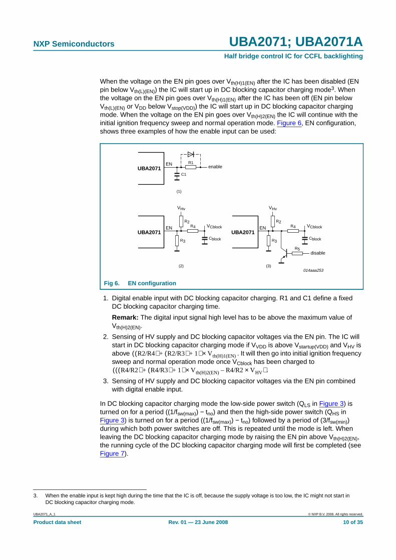
When the voltage on the EN pin goes over Vth(H)1(EN) after the IC has been disabled (ENpin below Vth(L)(EN)) the IC will start up in DC blocking capacitor charging mode3. Whenthe voltage on the EN pin goes over Vth(H)1(EN) after the IC has been off (EN pin belowVth(L)(EN) or VDD below Vstop(VDD)) the IC will start up in DC blocking capacitor chargingmode. When the voltage on the EN pin goes over Vth(H)2(EN) the IC will continue with theinitial ignition frequency sweep and normal operation mode. Figure 6, EN configuration,shows three examples of how the enable input can be used:
1. Digital enable input with DC blocking capacitor charging. R1 and C1 define a fixedDC blocking capacitor charging time.
Remark: The digital input signal high level has to be above the maximum value ofVth(H)2(EN).
2. Sensing of HV supply and DC blocking capacitor voltages via the EN pin. The IC willstart in DC blocking capacitor charging mode if VVDD is above Vstartup(VDD) and VHV isabove . It will then go into initial ignition frequencysweep and normal operation mode once VCblock has been charged to
.
3. Sensing of HV supply and DC blocking capacitor voltages via the EN pin combinedwith digital enable input.
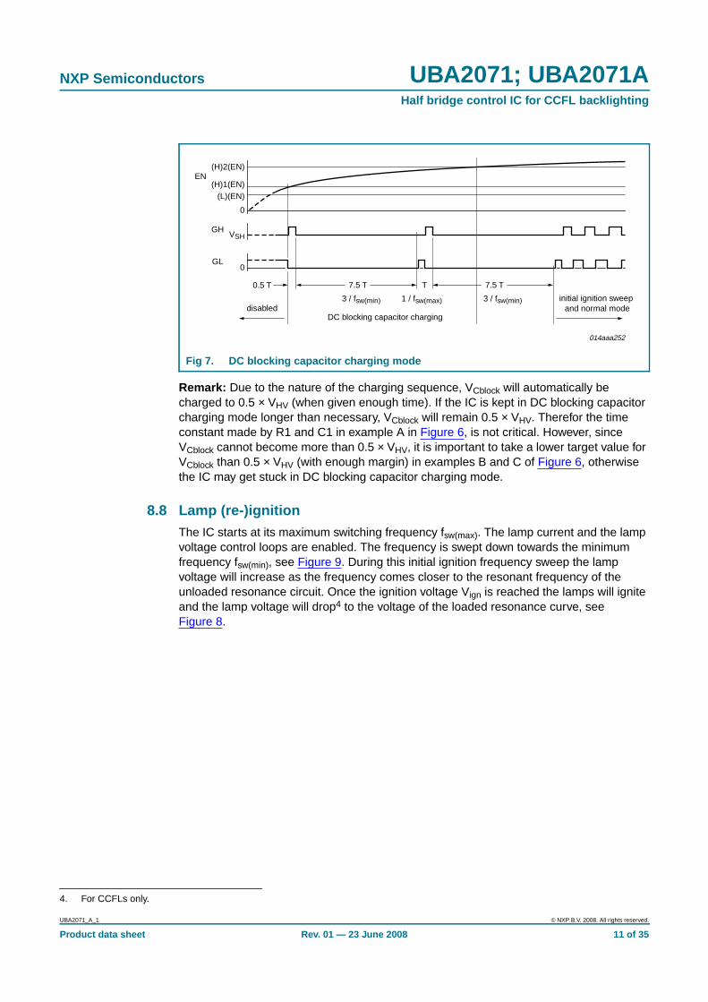
In DC blocking capacitor charging mode the low-side power switch (QLS in Figure 3) isturned on for a period ((1/fsw(max)) − tno) and then the high-side power switch (QHS inFigure 3) is turned on for a period ((1/fsw(max)) − tno) followed by a period of (3/fsw(min))during which both power switches are off. This is repeated until the mode is left. Whenleaving the DC blocking capacitor charging mode by raising the EN pin above Vth(H)2(EN),the running cycle of the DC blocking capacitor charging mode will first be completed (seeFigure 7).
3. When the enable input is kept high during the time that the IC is off, because the supply voltage is too low, the IC might not start inDC blocking capacitor charging mode.
Fig 6. EN configuration
014aaa253
UBA2071EN
C1
R1enable
(1)
UBA2071EN R4 VCblock
VHv
(2)
R3
R2
Cblock
UBA2071EN R4 VCblock
VHv
(3)
R3
R2
Cblock
R5disable
R2/R4( ) R2/R3( ) 1+ +( ) Vth(H)1(EN)×
R4/R2( ) R4/R3( ) 1++( ) Vth(H)2(EN) R4/R2 VHV×–×( )
UBA2071_A_1 © NXP B.V. 2008. All rights reserved.
Product data sheet Rev. 01 — 23 June 2008 10 of 35
NXP Semiconductors UBA2071; UBA2071AHalf bridge control IC for CCFL backlighting
Remark: Due to the nature of the charging sequence, VCblock will automatically becharged to 0.5 × VHV (when given enough time). If the IC is kept in DC blocking capacitorcharging mode longer than necessary, VCblock will remain 0.5 × VHV. Therefor the timeconstant made by R1 and C1 in example A in Figure 6, is not critical. However, sinceVCblock cannot become more than 0.5 × VHV, it is important to take a lower target value forVCblock than 0.5 × VHV (with enough margin) in examples B and C of Figure 6, otherwisethe IC may get stuck in DC blocking capacitor charging mode.
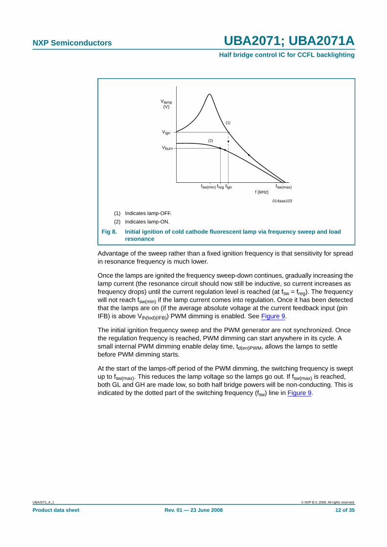
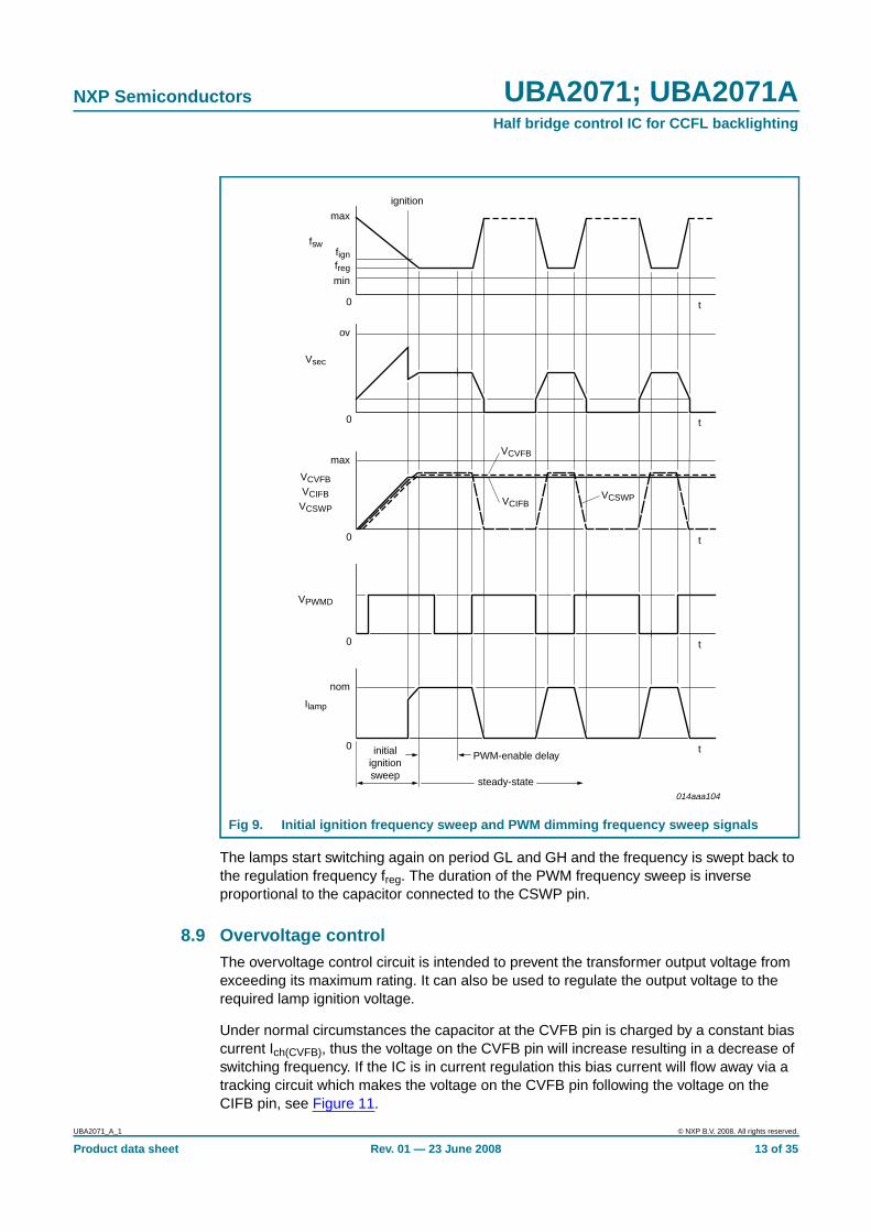
8.8 Lamp (re-)ignitionThe IC starts at its maximum switching frequency fsw(max). The lamp current and the lampvoltage control loops are enabled. The frequency is swept down towards the minimumfrequency fsw(min), see Figure 9. During this initial ignition frequency sweep the lampvoltage will increase as the frequency comes closer to the resonant frequency of theunloaded resonance circuit. Once the ignition voltage Vign is reached the lamps will igniteand the lamp voltage will drop4 to the voltage of the loaded resonance curve, seeFigure 8.
Fig 7. DC blocking capacitor charging mode
014aaa252
0
0
VSH
(L)(EN)(H)1(EN)
(H)2(EN)EN
GH
GL
disabledDC blocking capacitor charging
initial ignition sweep and normal mode
0.5 T T7.5 T 7.5 T
3 / fsw(min) 3 / fsw(min)1 / fsw(max)
4. For CCFLs only.
UBA2071_A_1 © NXP B.V. 2008. All rights reserved.
Product data sheet Rev. 01 — 23 June 2008 11 of 35
NXP Semiconductors UBA2071; UBA2071AHalf bridge control IC for CCFL backlighting
Advantage of the sweep rather than a fixed ignition frequency is that sensitivity for spreadin resonance frequency is much lower.
Once the lamps are ignited the frequency sweep-down continues, gradually increasing thelamp current (the resonance circuit should now still be inductive, so current increases asfrequency drops) until the current regulation level is reached (at fsw = freg). The frequencywill not reach fsw(min) if the lamp current comes into regulation. Once it has been detectedthat the lamps are on (if the average absolute voltage at the current feedback input (pinIFB) is above Vth(lod)(IFB)) PWM dimming is enabled. See Figure 9.
The initial ignition frequency sweep and the PWM generator are not synchronized. Oncethe regulation frequency is reached, PWM dimming can start anywhere in its cycle. Asmall internal PWM dimming enable delay time, td(en)PWM, allows the lamps to settlebefore PWM dimming starts.
At the start of the lamps-off period of the PWM dimming, the switching frequency is sweptup to fsw(max). This reduces the lamp voltage so the lamps go out. If fsw(max) is reached,both GL and GH are made low, so both half bridge powers will be non-conducting. This isindicated by the dotted part of the switching frequency (fsw) line in Figure 9.
(1) Indicates lamp-OFF.
(2) Indicates lamp-ON.
Fig 8. Initial ignition of cold cathode fluorescent lamp via frequency sweep and loadresonance
014aaa103
f (kHz)fsw(min) freg fign fsw(max)
Vlamp(V)
Vign
Vburn
(1)
(2)
UBA2071_A_1 © NXP B.V. 2008. All rights reserved.
Product data sheet Rev. 01 — 23 June 2008 12 of 35
NXP Semiconductors UBA2071; UBA2071AHalf bridge control IC for CCFL backlighting
The lamps start switching again on period GL and GH and the frequency is swept back tothe regulation frequency freg. The duration of the PWM frequency sweep is inverseproportional to the capacitor connected to the CSWP pin.
8.9 Overvoltage controlThe overvoltage control circuit is intended to prevent the transformer output voltage fromexceeding its maximum rating. It can also be used to regulate the output voltage to therequired lamp ignition voltage.
Under normal circumstances the capacitor at the CVFB pin is charged by a constant biascurrent Ich(CVFB), thus the voltage on the CVFB pin will increase resulting in a decrease ofswitching frequency. If the IC is in current regulation this bias current will flow away via atracking circuit which makes the voltage on the CVFB pin following the voltage on theCIFB pin, see Figure 11.
Fig 9. Initial ignition frequency sweep and PWM dimming frequency sweep signals
t
fsw
min
max
ignition
freg
fign
0
t
Vsec
ov
0
t
VCVFBVCIFB
VCSWP
max
0
t
VPWMD
0
t
Ilamp
0
nom
PWM-enable delay
014aaa104
steady-state
initialignitionsweep
VCVFB
VCIFBVCSWP
UBA2071_A_1 © NXP B.V. 2008. All rights reserved.
Product data sheet Rev. 01 — 23 June 2008 13 of 35
NXP Semiconductors UBA2071; UBA2071AHalf bridge control IC for CCFL backlighting
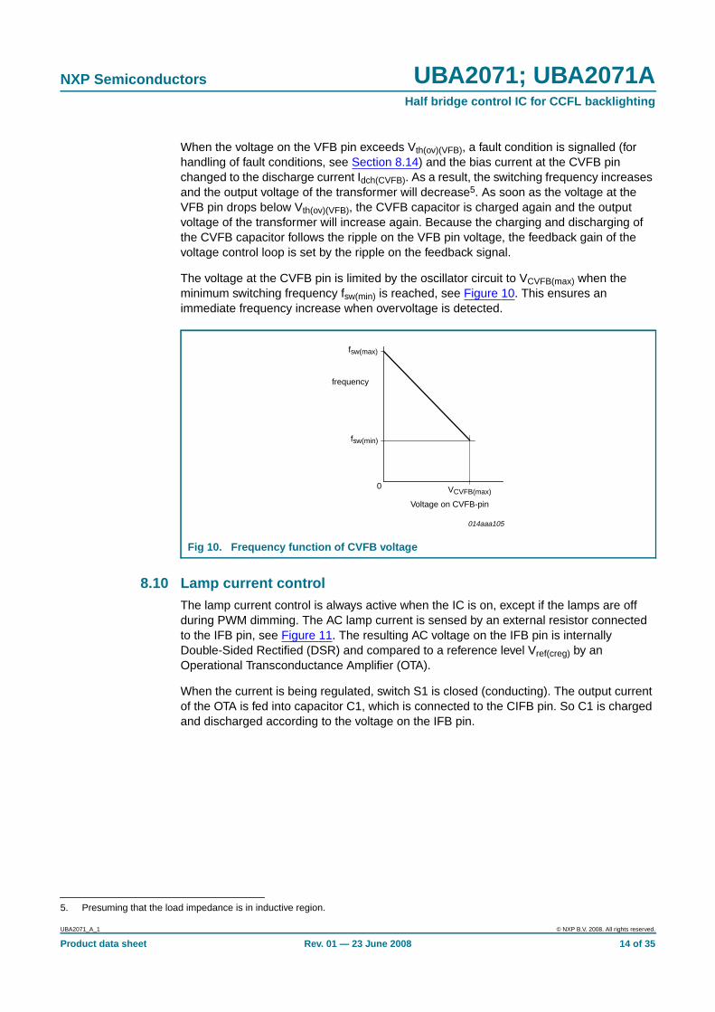
When the voltage on the VFB pin exceeds Vth(ov)(VFB), a fault condition is signalled (forhandling of fault conditions, see Section 8.14) and the bias current at the CVFB pinchanged to the discharge current Idch(CVFB). As a result, the switching frequency increasesand the output voltage of the transformer will decrease5. As soon as the voltage at theVFB pin drops below Vth(ov)(VFB), the CVFB capacitor is charged again and the outputvoltage of the transformer will increase again. Because the charging and discharging ofthe CVFB capacitor follows the ripple on the VFB pin voltage, the feedback gain of thevoltage control loop is set by the ripple on the feedback signal.
The voltage at the CVFB pin is limited by the oscillator circuit to VCVFB(max) when theminimum switching frequency fsw(min) is reached, see Figure 10. This ensures animmediate frequency increase when overvoltage is detected.
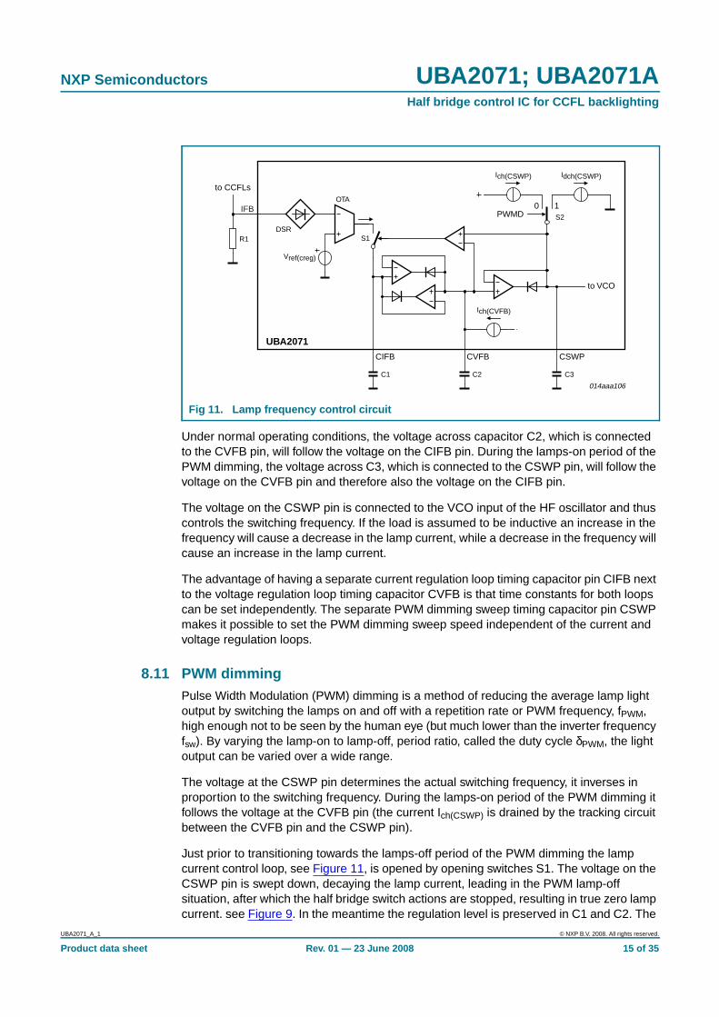
8.10 Lamp current controlThe lamp current control is always active when the IC is on, except if the lamps are offduring PWM dimming. The AC lamp current is sensed by an external resistor connectedto the IFB pin, see Figure 11. The resulting AC voltage on the IFB pin is internallyDouble-Sided Rectified (DSR) and compared to a reference level Vref(creg) by anOperational Transconductance Amplifier (OTA).
When the current is being regulated, switch S1 is closed (conducting). The output currentof the OTA is fed into capacitor C1, which is connected to the CIFB pin. So C1 is chargedand discharged according to the voltage on the IFB pin.
5. Presuming that the load impedance is in inductive region.
Fig 10. Frequency function of CVFB voltage
Voltage on CVFB-pin
frequency
fsw(min)
fsw(max)
0 VCVFB(max)
014aaa105
UBA2071_A_1 © NXP B.V. 2008. All rights reserved.
Product data sheet Rev. 01 — 23 June 2008 14 of 35
NXP Semiconductors UBA2071; UBA2071AHalf bridge control IC for CCFL backlighting
Under normal operating conditions, the voltage across capacitor C2, which is connectedto the CVFB pin, will follow the voltage on the CIFB pin. During the lamps-on period of thePWM dimming, the voltage across C3, which is connected to the CSWP pin, will follow thevoltage on the CVFB pin and therefore also the voltage on the CIFB pin.
The voltage on the CSWP pin is connected to the VCO input of the HF oscillator and thuscontrols the switching frequency. If the load is assumed to be inductive an increase in thefrequency will cause a decrease in the lamp current, while a decrease in the frequency willcause an increase in the lamp current.
The advantage of having a separate current regulation loop timing capacitor pin CIFB nextto the voltage regulation loop timing capacitor CVFB is that time constants for both loopscan be set independently. The separate PWM dimming sweep timing capacitor pin CSWPmakes it possible to set the PWM dimming sweep speed independent of the current andvoltage regulation loops.
8.11 PWM dimmingPulse Width Modulation (PWM) dimming is a method of reducing the average lamp lightoutput by switching the lamps on and off with a repetition rate or PWM frequency, fPWM,high enough not to be seen by the human eye (but much lower than the inverter frequencyfsw). By varying the lamp-on to lamp-off, period ratio, called the duty cycle δPWM, the lightoutput can be varied over a wide range.
The voltage at the CSWP pin determines the actual switching frequency, it inverses inproportion to the switching frequency. During the lamps-on period of the PWM dimming itfollows the voltage at the CVFB pin (the current Ich(CSWP) is drained by the tracking circuitbetween the CVFB pin and the CSWP pin).
Just prior to transitioning towards the lamps-off period of the PWM dimming the lampcurrent control loop, see Figure 11, is opened by opening switches S1. The voltage on theCSWP pin is swept down, decaying the lamp current, leading in the PWM lamp-offsituation, after which the half bridge switch actions are stopped, resulting in true zero lampcurrent. see Figure 9. In the meantime the regulation level is preserved in C1 and C2. The
Fig 11. Lamp frequency control circuit
R1
C1
to CCFLs
DSR
Vref(creg)
C2 C3
Ich(CSWP)
PWMD0 1
Idch(CSWP)
S2
S1
to VCO
Ich(CVFB)
CIFB CVFB CSWP
UBA2071
OTA
014aaa106
IFB
UBA2071_A_1 © NXP B.V. 2008. All rights reserved.
Product data sheet Rev. 01 — 23 June 2008 15 of 35
NXP Semiconductors UBA2071; UBA2071AHalf bridge control IC for CCFL backlighting
PWM lamp-on situation is reached again through a reverse sequence of events, startingthe half bridge actions, increasing the voltage on CSWP, increasing the lamp current backto the controlled value. Switch S1 is closed (conducting) again when the voltage on theCSWP pin has reached the voltage on the CVFB pin again.
The IC waits until the CSWP sweep-up6 has reached the current/voltage control level atthe CVFB pin before sweeping down. This prevents the lamps from going out completelywhen deep dimming on CSWP pin is combined with a large value capacitor.
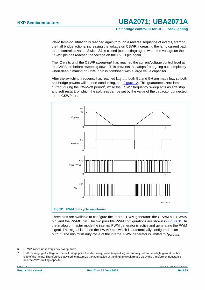
After the switching frequency has reached fsw(max), both GL and GH are made low, so bothhalf bridge powers will be non-conducting, see Figure 12. This guarantees zero lampcurrent during the PWM-off period7, while the CSWP frequency sweep acts as soft stopand soft restart, of which the softness can be set by the value of the capacitor connectedto the CSWP pin.
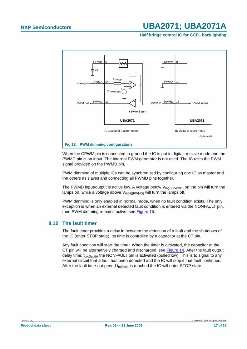
Three pins are available to configure the internal PWM generator: the CPWM pin, PWMApin, and the PWMD pin. The two possible PWM configurations are shown in Figure 13. Inthe analog or master mode the internal PWM generator is active and generating the PWMsignal. This signal is put on the PWMD pin, which is automatically configured as anoutput. The minimum duty cycle of the internal PWM generator is limited to δPWM(min).
6. CSWP sweep-up is frequency sweep-down.
7. Until the ringing of voltage on the half bridge point has died away, some (capacitive) current may still cause a light glow at the hotside of the lamps. Therefore it is advised to maximize the attenuation of the ringing circuit (made up by the transformer inductanceand the ∆V/∆t limiting capacitor).
Fig 12. PWM dim cycle waveforms
t
VCSWP
maxreg
5 V
VDD
VDD
0
t
VPWMD
0
t
VGH − VSH
0
t
VGL
0
014aaa107
UBA2071_A_1 © NXP B.V. 2008. All rights reserved.
Product data sheet Rev. 01 — 23 June 2008 16 of 35
NXP Semiconductors UBA2071; UBA2071AHalf bridge control IC for CCFL backlighting
When the CPWM pin is connected to ground the IC is put in digital or slave mode and thePWMD pin is an input. The internal PWM generator is not used. The IC uses the PWMsignal provided on the PWMD pin.
PWM dimming of multiple ICs can be synchronized by configuring one IC as master andthe others as slaves and connecting all PWMD pins together.
The PWMD input/output is active low. A voltage below Vth(L)(PWMD) on the pin will turn thelamps on, while a voltage above Vth(H)(PWMD) will turn the lamps off.
PWM dimming is only enabled in normal mode, when no fault condition exists. The onlyexception is when an external detected fault condition is entered via the NONFAULT pin,then PWM dimming remains active, see Figure 15.
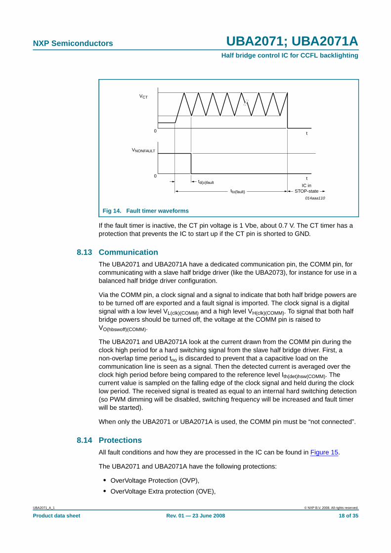
8.12 The fault timerThe fault timer provides a delay in between the detection of a fault and the shutdown ofthe IC (enter STOP state). Its time is controlled by a capacitor at the CT pin.
Any fault condition will start the timer. When the timer is activated, the capacitor at theCT pin will be alternatively charged and discharged, see Figure 14. After the fault outputdelay time, td(o)fault), the NONFAULT pin is activated (pulled low). This is to signal to anyexternal circuit that a fault has been detected and the IC will stop if that fault continues.After the fault time-out period tto(fault) is reached the IC will enter STOP state.
Fig 13. PWM dimming configurations
C1
RPWMAPWMAanalog in
PWM out
CPWM 9
PWMD
VPWMA(ref)
14
13
PWM intern
UBA2071
A: analog or master mode
PWM in
UBA2071
B: digital or slave mode
PWM intern
014aaa108
PWMA
CPWM 9
PWMD
14
13
UBA2071_A_1 © NXP B.V. 2008. All rights reserved.
Product data sheet Rev. 01 — 23 June 2008 17 of 35
NXP Semiconductors UBA2071; UBA2071AHalf bridge control IC for CCFL backlighting
If the fault timer is inactive, the CT pin voltage is 1 Vbe, about 0.7 V. The CT timer has aprotection that prevents the IC to start up if the CT pin is shorted to GND.
8.13 CommunicationThe UBA2071 and UBA2071A have a dedicated communication pin, the COMM pin, forcommunicating with a slave half bridge driver (like the UBA2073), for instance for use in abalanced half bridge driver configuration.
Via the COMM pin, a clock signal and a signal to indicate that both half bridge powers areto be turned off are exported and a fault signal is imported. The clock signal is a digitalsignal with a low level VL(clk)(COMM) and a high level VH(clk)(COMM). To signal that both halfbridge powers should be turned off, the voltage at the COMM pin is raised toVO(hbswoff)(COMM).
The UBA2071 and UBA2071A look at the current drawn from the COMM pin during theclock high period for a hard switching signal from the slave half bridge driver. First, anon-overlap time period tno is discarded to prevent that a capacitive load on thecommunication line is seen as a signal. Then the detected current is averaged over theclock high period before being compared to the reference level Ith(det)hsw(COMM). Thecurrent value is sampled on the falling edge of the clock signal and held during the clocklow period. The received signal is treated as equal to an internal hard switching detection(so PWM dimming will be disabled, switching frequency will be increased and fault timerwill be started).
When only the UBA2071 or UBA2071A is used, the COMM pin must be “not connected”.
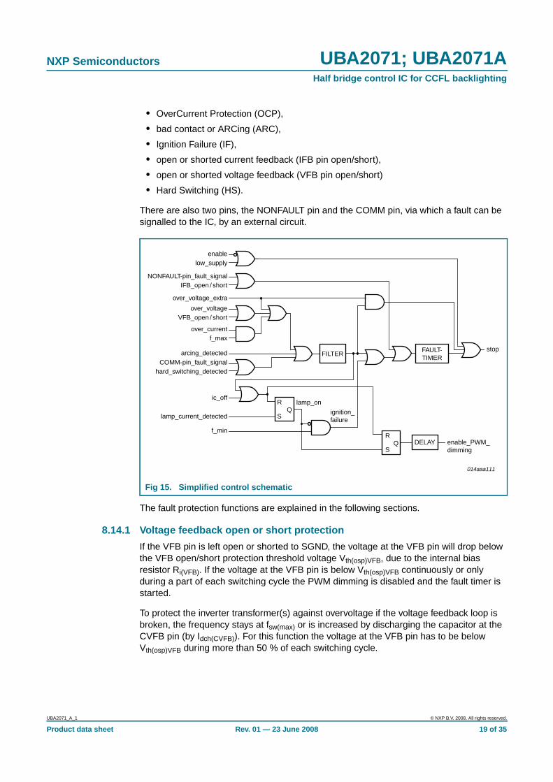
8.14 ProtectionsAll fault conditions and how they are processed in the IC can be found in Figure 15.
The UBA2071 and UBA2071A have the following protections:
• OverVoltage Protection (OVP),
• OverVoltage Extra protection (OVE),
Fig 14. Fault timer waveforms
t
VCT
0
t
VNONFAULT
0
IC inSTOP-state
td(o)fault
014aaa110
tto(fault)
UBA2071_A_1 © NXP B.V. 2008. All rights reserved.
Product data sheet Rev. 01 — 23 June 2008 18 of 35
NXP Semiconductors UBA2071; UBA2071AHalf bridge control IC for CCFL backlighting
• OverCurrent Protection (OCP),
• bad contact or ARCing (ARC),
• Ignition Failure (IF),
• open or shorted current feedback (IFB pin open/short),
• open or shorted voltage feedback (VFB pin open/short)
• Hard Switching (HS).
There are also two pins, the NONFAULT pin and the COMM pin, via which a fault can besignalled to the IC, by an external circuit.
The fault protection functions are explained in the following sections.
8.14.1 Voltage feedback open or short protection
If the VFB pin is left open or shorted to SGND, the voltage at the VFB pin will drop belowthe VFB open/short protection threshold voltage Vth(osp)VFB, due to the internal biasresistor Ri(VFB). If the voltage at the VFB pin is below Vth(osp)VFB continuously or onlyduring a part of each switching cycle the PWM dimming is disabled and the fault timer isstarted.
To protect the inverter transformer(s) against overvoltage if the voltage feedback loop isbroken, the frequency stays at fsw(max) or is increased by discharging the capacitor at theCVFB pin (by Idch(CVFB)). For this function the voltage at the VFB pin has to be belowVth(osp)VFB during more than 50 % of each switching cycle.
Fig 15. Simplified control schematic
enablelow_supply
NONFAULT-pin_fault_signalIFB_open / short
over_voltage_extra
over_voltageVFB_open / short
COMM-pin_fault_signalhard_switching_detected
over_currentf_max
arcing_detected
lamp_current_detected
f_min
ic_off
FAULT-TIMER
FILTERstop
R
SQ
lamp_on
ignition_failure
R
SQ DELAY enable_PWM_
dimming
014aaa111
UBA2071_A_1 © NXP B.V. 2008. All rights reserved.
Product data sheet Rev. 01 — 23 June 2008 19 of 35
NXP Semiconductors UBA2071; UBA2071AHalf bridge control IC for CCFL backlighting
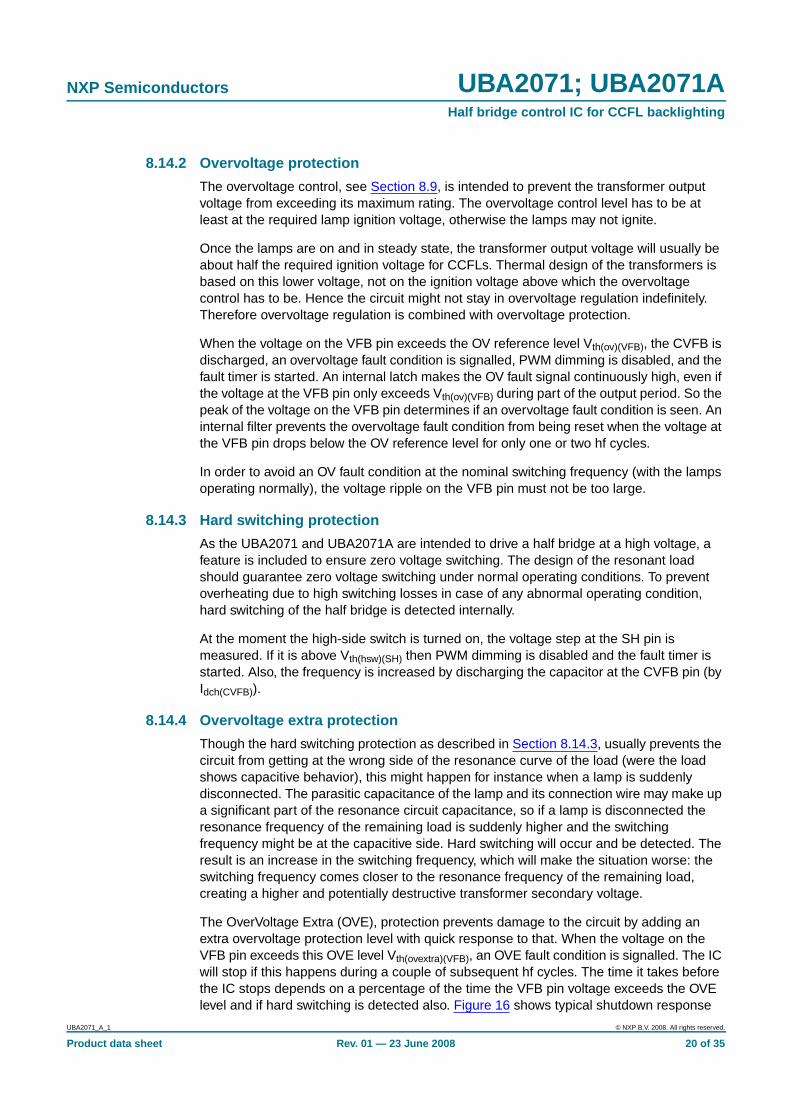
8.14.2 Overvoltage protection
The overvoltage control, see Section 8.9, is intended to prevent the transformer outputvoltage from exceeding its maximum rating. The overvoltage control level has to be atleast at the required lamp ignition voltage, otherwise the lamps may not ignite.
Once the lamps are on and in steady state, the transformer output voltage will usually beabout half the required ignition voltage for CCFLs. Thermal design of the transformers isbased on this lower voltage, not on the ignition voltage above which the overvoltagecontrol has to be. Hence the circuit might not stay in overvoltage regulation indefinitely.Therefore overvoltage regulation is combined with overvoltage protection.
When the voltage on the VFB pin exceeds the OV reference level Vth(ov)(VFB), the CVFB isdischarged, an overvoltage fault condition is signalled, PWM dimming is disabled, and thefault timer is started. An internal latch makes the OV fault signal continuously high, even ifthe voltage at the VFB pin only exceeds Vth(ov)(VFB) during part of the output period. So thepeak of the voltage on the VFB pin determines if an overvoltage fault condition is seen. Aninternal filter prevents the overvoltage fault condition from being reset when the voltage atthe VFB pin drops below the OV reference level for only one or two hf cycles.
In order to avoid an OV fault condition at the nominal switching frequency (with the lampsoperating normally), the voltage ripple on the VFB pin must not be too large.
8.14.3 Hard switching protection
As the UBA2071 and UBA2071A are intended to drive a half bridge at a high voltage, afeature is included to ensure zero voltage switching. The design of the resonant loadshould guarantee zero voltage switching under normal operating conditions. To preventoverheating due to high switching losses in case of any abnormal operating condition,hard switching of the half bridge is detected internally.
At the moment the high-side switch is turned on, the voltage step at the SH pin ismeasured. If it is above Vth(hsw)(SH) then PWM dimming is disabled and the fault timer isstarted. Also, the frequency is increased by discharging the capacitor at the CVFB pin (byIdch(CVFB)).
8.14.4 Overvoltage extra protection
Though the hard switching protection as described in Section 8.14.3, usually prevents thecircuit from getting at the wrong side of the resonance curve of the load (were the loadshows capacitive behavior), this might happen for instance when a lamp is suddenlydisconnected. The parasitic capacitance of the lamp and its connection wire may make upa significant part of the resonance circuit capacitance, so if a lamp is disconnected theresonance frequency of the remaining load is suddenly higher and the switchingfrequency might be at the capacitive side. Hard switching will occur and be detected. Theresult is an increase in the switching frequency, which will make the situation worse: theswitching frequency comes closer to the resonance frequency of the remaining load,creating a higher and potentially destructive transformer secondary voltage.
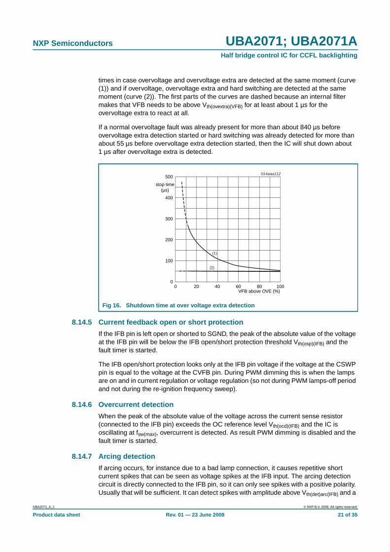
The OverVoltage Extra (OVE), protection prevents damage to the circuit by adding anextra overvoltage protection level with quick response to that. When the voltage on theVFB pin exceeds this OVE level Vth(ovextra)(VFB), an OVE fault condition is signalled. The ICwill stop if this happens during a couple of subsequent hf cycles. The time it takes beforethe IC stops depends on a percentage of the time the VFB pin voltage exceeds the OVElevel and if hard switching is detected also. Figure 16 shows typical shutdown response
UBA2071_A_1 © NXP B.V. 2008. All rights reserved.
Product data sheet Rev. 01 — 23 June 2008 20 of 35
NXP Semiconductors UBA2071; UBA2071AHalf bridge control IC for CCFL backlighting
times in case overvoltage and overvoltage extra are detected at the same moment (curve(1)) and if overvoltage, overvoltage extra and hard switching are detected at the samemoment (curve (2)). The first parts of the curves are dashed because an internal filtermakes that VFB needs to be above Vth(ovextra)(VFB) for at least about 1 µs for theovervoltage extra to react at all.
If a normal overvoltage fault was already present for more than about 840 µs beforeovervoltage extra detection started or hard switching was already detected for more thanabout 55 µs before overvoltage extra detection started, then the IC will shut down about1 µs after overvoltage extra is detected.
8.14.5 Current feedback open or short protection
If the IFB pin is left open or shorted to SGND, the peak of the absolute value of the voltageat the IFB pin will be below the IFB open/short protection threshold Vth(osp)(IFB) and thefault timer is started.
The IFB open/short protection looks only at the IFB pin voltage if the voltage at the CSWPpin is equal to the voltage at the CVFB pin. During PWM dimming this is when the lampsare on and in current regulation or voltage regulation (so not during PWM lamps-off periodand not during the re-ignition frequency sweep).
8.14.6 Overcurrent detection
When the peak of the absolute value of the voltage across the current sense resistor(connected to the IFB pin) exceeds the OC reference level Vth(ocd)(IFB) and the IC isoscillating at fsw(max), overcurrent is detected. As result PWM dimming is disabled and thefault timer is started.
8.14.7 Arcing detection
If arcing occurs, for instance due to a bad lamp connection, it causes repetitive shortcurrent spikes that can be seen as voltage spikes at the IFB input. The arcing detectioncircuit is directly connected to the IFB pin, so it can only see spikes with a positive polarity.Usually that will be sufficient. It can detect spikes with amplitude above Vth(det)arc(IFB) and a
Fig 16. Shutdown time at over voltage extra detection
VFB above OVE (%)0 1008040 6020
014aaa112
200
300
100
400
500
stop time(µs)
0
(1)
(2)
UBA2071_A_1 © NXP B.V. 2008. All rights reserved.
Product data sheet Rev. 01 — 23 June 2008 21 of 35
NXP Semiconductors UBA2071; UBA2071AHalf bridge control IC for CCFL backlighting
duration longer than tspike(min). Each spike will trigger an internal one-shot, which signals tothe control circuits that arcing has been detected. When arcing is detected, PWM dimmingis disabled and the fault timer is started.
8.14.8 Ignition Failure (IF)
When the current control loop comes close to its regulation point, the lamps are assumedto be on (ignited). This is when the average absolute voltage on the IFB pin is aboveVth(lod)(IFB). If the lamps are not on when the ignition sweep is finished, (switchingfrequency has reached fsw(min)), then an ignition failure is detected, PWM dimming isdisabled and the fault timer is started.
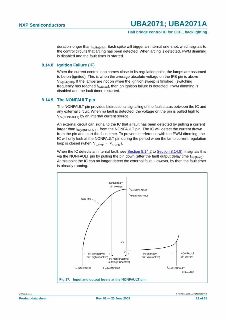
8.14.9 The NONFAULT pin
The NONFAULT pin provides bidirectional signalling of the fault status between the IC andany external circuit. When no fault is detected, the voltage on the pin is pulled high toVoc(NONFAULT) by an internal current source.
An external circuit can signal to the IC that a fault has been detected by pulling a currentlarger than Itrig(I)NONFAULT from the NONFAULT pin. The IC will detect the current drawnfrom the pin and start the fault timer. To prevent interference with the PWM dimming, theIC will only look at the NONFAULT pin during the period when the lamp current regulationloop is closed (when ).
When the IC detects an internal fault, see Section 8.14.2 to Section 8.14.8), it signals thisvia the NONFAULT pin by pulling the pin down (after the fault output delay time td(o)fault)).At this point the IC can no longer detect the external fault. However, by then the fault timeris already running.
Fig 17. Input and output levels at the NONFAULT pin
VCSWP VCVFB=
Isink(NONFAULT)
NONFAULTpin current
NONFAULTpin voltage
0
Vtrig(I)NONFAULT
Voc(NONFAULT)
in: low (active) out: high (inactive)
in: unknown out: low (active)
Itrig(I)NONFAULTIsc(NONFAULT)
in: high (inactive)out: high (inactive)
load line
014aaa113
1 V
UBA2071_A_1 © NXP B.V. 2008. All rights reserved.
Product data sheet Rev. 01 — 23 June 2008 22 of 35
NXP Semiconductors UBA2071; UBA2071AHalf bridge control IC for CCFL backlighting
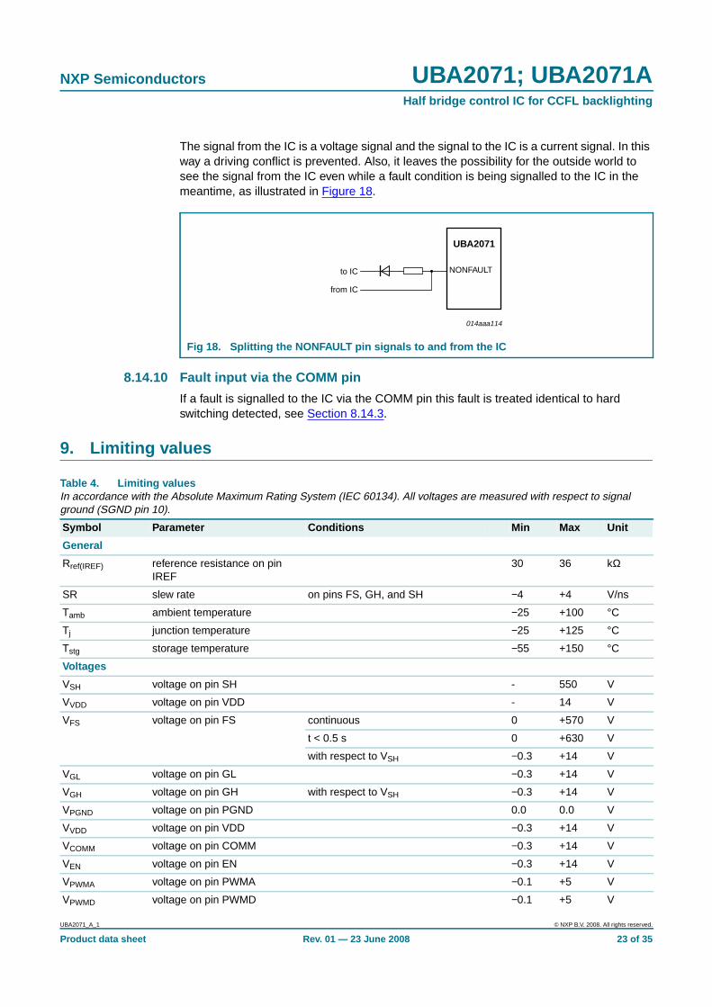
The signal from the IC is a voltage signal and the signal to the IC is a current signal. In thisway a driving conflict is prevented. Also, it leaves the possibility for the outside world tosee the signal from the IC even while a fault condition is being signalled to the IC in themeantime, as illustrated in Figure 18.
8.14.10 Fault input via the COMM pin
If a fault is signalled to the IC via the COMM pin this fault is treated identical to hardswitching detected, see Section 8.14.3.
9. Limiting values
Fig 18. Splitting the NONFAULT pin signals to and from the IC
UBA2071
to IC
from IC
NONFAULT
014aaa114
Table 4. Limiting valuesIn accordance with the Absolute Maximum Rating System (IEC 60134). All voltages are measured with respect to signalground (SGND pin 10).
Symbol Parameter Conditions Min Max Unit
General
Rref(IREF) reference resistance on pinIREF
30 36 kΩ
SR slew rate on pins FS, GH, and SH −4 +4 V/ns
Tamb ambient temperature −25 +100 °C
Tj junction temperature −25 +125 °C
Tstg storage temperature −55 +150 °C
Voltages
VSH voltage on pin SH - 550 V
VVDD voltage on pin VDD - 14 V
VFS voltage on pin FS continuous 0 +570 V
t < 0.5 s 0 +630 V
with respect to VSH −0.3 +14 V
VGL voltage on pin GL −0.3 +14 V
VGH voltage on pin GH with respect to VSH −0.3 +14 V
VPGND voltage on pin PGND 0.0 0.0 V
VVDD voltage on pin VDD −0.3 +14 V
VCOMM voltage on pin COMM −0.3 +14 V
VEN voltage on pin EN −0.3 +14 V
VPWMA voltage on pin PWMA −0.1 +5 V
VPWMD voltage on pin PWMD −0.1 +5 V
UBA2071_A_1 © NXP B.V. 2008. All rights reserved.
Product data sheet Rev. 01 — 23 June 2008 23 of 35
NXP Semiconductors UBA2071; UBA2071AHalf bridge control IC for CCFL backlighting
10. Thermal characteristics
11. Characteristics
VNONFAULT voltage on pin NONFAULT −0.1 +5 V
VVFB voltage on pin VFB continuous −0.1 +5 V
t < 1 ms −0.1 +9 V
VIFB voltage on pin IFB continuous −5 +5 V
t < 1 ms −9 +9 V
ESD
VESD electrostatic discharge voltage human body model:
pins IFB, CIFB, VFB, CVFB,CSWP, IREF, CT, CF, CPWM,NONFAULT, COMM, PWMA,PWMD, EN, VDD, and GL
−2 +2 kV
pins GH, FS, and SH −1 +1 kV
machine model:
all pins −250 +250 V
Table 4. Limiting values …continuedIn accordance with the Absolute Maximum Rating System (IEC 60134). All voltages are measured with respect to signalground (SGND pin 10).
Symbol Parameter Conditions Min Max Unit
Table 5. Thermal characteristics
Symbol Parameter Conditions Typ Unit
Rth(j-a) thermal resistance fromjunction to ambient
in free air; SO24 package 80 K/W
in free air; SSOP24 package 111 K/W
Table 6. CharacteristicsTamb = 25 °C; VVDD = 12 V; RIREF = 33 kΩ; VEN = VVDD and CPWM connected to a capacitor, unless otherwise specified. Allvoltages are measured with respect to signal ground (SGND, pin 10). SGND and PGND connected together. GL, GH,COMM, NONFAULT and PWMD pins left open (unless otherwise specified). Currents are positive when flowing into the IC.Parameters valid for all types (unless otherwise specified).
Symbol Parameter Conditions Min Typ Max Unit
High voltage
Ileak leakage current VFS, VGH, and VSH = 630 V;VVDD = 0 V
- - 2 µA
Start-up
Vstartup(VDD) VDD start-up voltage UBA2071T and UBA2071TS 11.7 12.1 12.5 V
UBA2071AT and UBA2071ATS 10.5 10.9 11.3 V
Vstop(VDD) stop voltage on pin VDD 9.8 10.1 10.4 V
Vhys(VDD) hysteresis voltage on pin VDD UBA2071T and UBA2071TS 1.8 2 2.2 V
UBA2071AT and UBA2071ATS 0.6 0.8 1.0 V
Istartup(VDD) start-up current on pin VDD VVDD = 11 V; EN pin grounded 0.13 0.16 0.19 mA
UBA2071_A_1 © NXP B.V. 2008. All rights reserved.
Product data sheet Rev. 01 — 23 June 2008 24 of 35
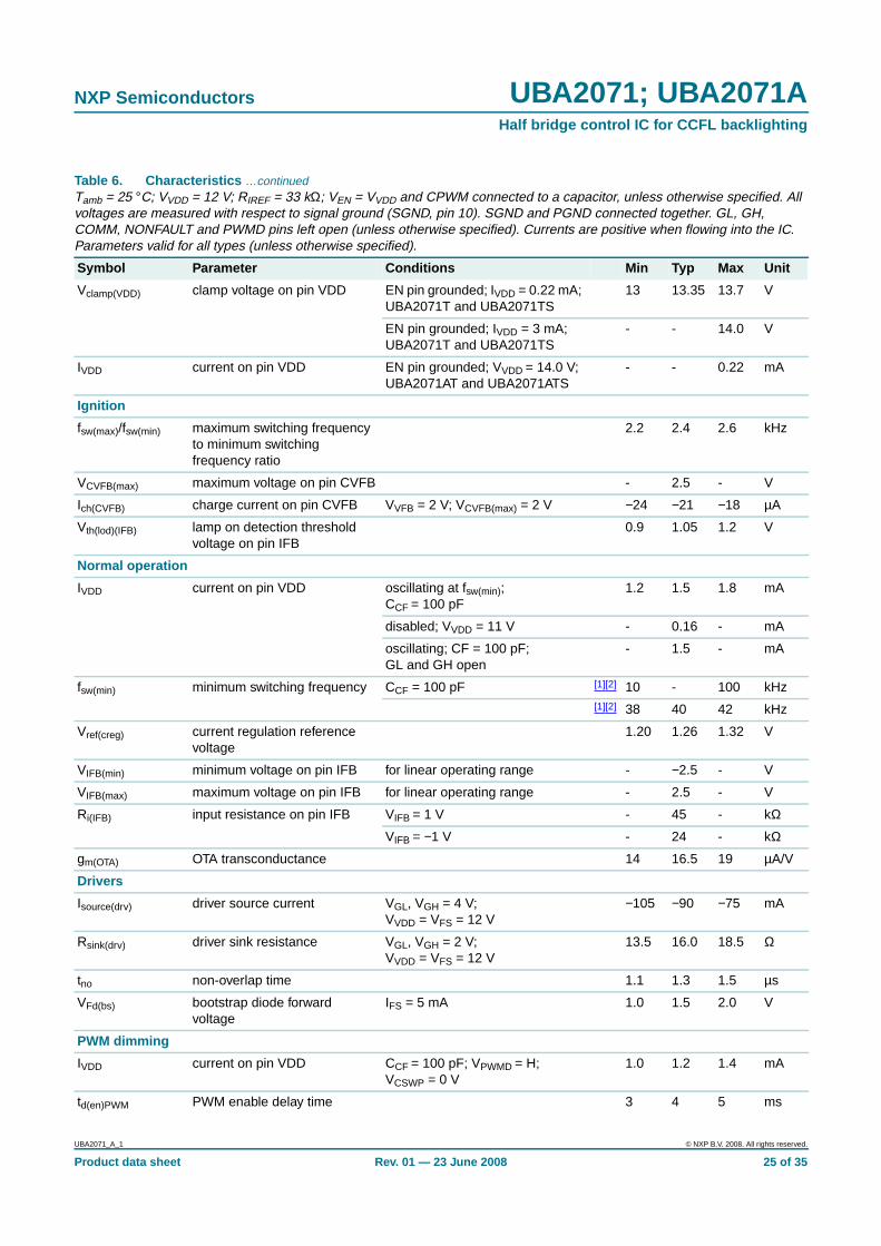
NXP Semiconductors UBA2071; UBA2071AHalf bridge control IC for CCFL backlighting
Vclamp(VDD) clamp voltage on pin VDD EN pin grounded; IVDD = 0.22 mA;UBA2071T and UBA2071TS
13 13.35 13.7 V
EN pin grounded; IVDD = 3 mA;UBA2071T and UBA2071TS
- - 14.0 V
IVDD current on pin VDD EN pin grounded; VVDD = 14.0 V;UBA2071AT and UBA2071ATS
- - 0.22 mA
Ignition
fsw(max)/fsw(min) maximum switching frequencyto minimum switchingfrequency ratio
2.2 2.4 2.6 kHz
VCVFB(max) maximum voltage on pin CVFB - 2.5 - V
Ich(CVFB) charge current on pin CVFB VVFB = 2 V; VCVFB(max) = 2 V −24 −21 −18 µA
Vth(lod)(IFB) lamp on detection thresholdvoltage on pin IFB
0.9 1.05 1.2 V
Normal operation
IVDD current on pin VDD oscillating at fsw(min);CCF = 100 pF
1.2 1.5 1.8 mA
disabled; VVDD = 11 V - 0.16 - mA
oscillating; CF = 100 pF;GL and GH open
- 1.5 - mA
fsw(min) minimum switching frequency CCF = 100 pF [1][2] 10 - 100 kHz[1][2] 38 40 42 kHz
Vref(creg) current regulation referencevoltage
1.20 1.26 1.32 V
VIFB(min) minimum voltage on pin IFB for linear operating range - −2.5 - V
VIFB(max) maximum voltage on pin IFB for linear operating range - 2.5 - V
Ri(IFB) input resistance on pin IFB VIFB = 1 V - 45 - kΩ
VIFB = −1 V - 24 - kΩ
gm(OTA) OTA transconductance 14 16.5 19 µA/V
Drivers
Isource(drv) driver source current VGL, VGH = 4 V;VVDD = VFS = 12 V
−105 −90 −75 mA
Rsink(drv) driver sink resistance VGL, VGH = 2 V;VVDD = VFS = 12 V
13.5 16.0 18.5 Ω
tno non-overlap time 1.1 1.3 1.5 µs
VFd(bs) bootstrap diode forwardvoltage
IFS = 5 mA 1.0 1.5 2.0 V
PWM dimming
IVDD current on pin VDD CCF = 100 pF; VPWMD = H;VCSWP = 0 V
1.0 1.2 1.4 mA
td(en)PWM PWM enable delay time 3 4 5 ms
Table 6. Characteristics …continuedTamb = 25 °C; VVDD = 12 V; RIREF = 33 kΩ; VEN = VVDD and CPWM connected to a capacitor, unless otherwise specified. Allvoltages are measured with respect to signal ground (SGND, pin 10). SGND and PGND connected together. GL, GH,COMM, NONFAULT and PWMD pins left open (unless otherwise specified). Currents are positive when flowing into the IC.Parameters valid for all types (unless otherwise specified).
Symbol Parameter Conditions Min Typ Max Unit
UBA2071_A_1 © NXP B.V. 2008. All rights reserved.
Product data sheet Rev. 01 — 23 June 2008 25 of 35
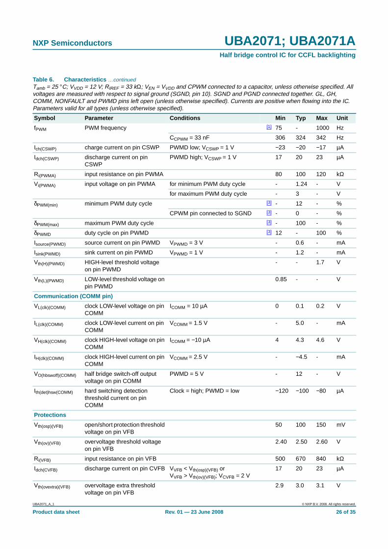
NXP Semiconductors UBA2071; UBA2071AHalf bridge control IC for CCFL backlighting
fPWM PWM frequency [1] 75 - 1000 Hz
CCPWM = 33 nF 306 324 342 Hz
Ich(CSWP) charge current on pin CSWP PWMD low; VCSWP = 1 V −23 −20 −17 µA
Idch(CSWP) discharge current on pinCSWP
PWMD high; VCSWP = 1 V 17 20 23 µA
Ri(PWMA) input resistance on pin PWMA 80 100 120 kΩ
Vi(PWMA) input voltage on pin PWMA for minimum PWM duty cycle - 1.24 - V
for maximum PWM duty cycle - 3 - V
δPWM(min) minimum PWM duty cycle [3] - 12 - %
CPWM pin connected to SGND [3] - 0 - %
δPWM(max) maximum PWM duty cycle [3] - 100 - %
δPWMD duty cycle on pin PWMD [3] 12 - 100 %
Isource(PWMD) source current on pin PWMD VPWMD = 3 V - 0.6 - mA
Isink(PWMD) sink current on pin PWMD VPWMD = 1 V - 1.2 - mA
Vth(H)(PWMD) HIGH-level threshold voltageon pin PWMD
- - 1.7 V
Vth(L)(PWMD) LOW-level threshold voltage onpin PWMD
0.85 - - V
Communication (COMM pin)
VL(clk)(COMM) clock LOW-level voltage on pinCOMM
ICOMM = 10 µA 0 0.1 0.2 V
IL(clk)(COMM) clock LOW-level current on pinCOMM
VCOMM = 1.5 V - 5.0 - mA
VH(clk)(COMM) clock HIGH-level voltage on pinCOMM
ICOMM = −10 µA 4 4.3 4.6 V
IH(clk)(COMM) clock HIGH-level current on pinCOMM
VCOMM = 2.5 V - −4.5 - mA
VO(hbswoff)(COMM) half bridge switch-off outputvoltage on pin COMM
PWMD = 5 V - 12 - V
Ith(det)hsw(COMM) hard switching detectionthreshold current on pinCOMM
Clock = high; PWMD = low −120 −100 −80 µA
Protections
Vth(osp)(VFB) open/short protection thresholdvoltage on pin VFB
50 100 150 mV
Vth(ov)(VFB) overvoltage threshold voltageon pin VFB
2.40 2.50 2.60 V
Ri(VFB) input resistance on pin VFB 500 670 840 kΩ
Idch(CVFB) discharge current on pin CVFB VVFB < Vth(osp)(VFB) orVVFB > Vth(ov)(VFB); VCVFB = 2 V
17 20 23 µA
Vth(ovextra)(VFB) overvoltage extra thresholdvoltage on pin VFB
2.9 3.0 3.1 V
Table 6. Characteristics …continuedTamb = 25 °C; VVDD = 12 V; RIREF = 33 kΩ; VEN = VVDD and CPWM connected to a capacitor, unless otherwise specified. Allvoltages are measured with respect to signal ground (SGND, pin 10). SGND and PGND connected together. GL, GH,COMM, NONFAULT and PWMD pins left open (unless otherwise specified). Currents are positive when flowing into the IC.Parameters valid for all types (unless otherwise specified).
Symbol Parameter Conditions Min Typ Max Unit
UBA2071_A_1 © NXP B.V. 2008. All rights reserved.
Product data sheet Rev. 01 — 23 June 2008 26 of 35
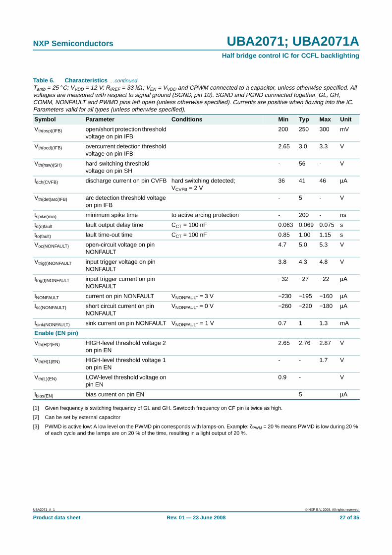
NXP Semiconductors UBA2071; UBA2071AHalf bridge control IC for CCFL backlighting
[1] Given frequency is switching frequency of GL and GH. Sawtooth frequency on CF pin is twice as high.
[2] Can be set by external capacitor
[3] PWMD is active low: A low level on the PWMD pin corresponds with lamps-on. Example: δPWM = 20 % means PWMD is low during 20 %of each cycle and the lamps are on 20 % of the time, resulting in a light output of 20 %.
Vth(osp)(IFB) open/short protection thresholdvoltage on pin IFB
200 250 300 mV
Vth(ocd)(IFB) overcurrent detection thresholdvoltage on pin IFB
2.65 3.0 3.3 V
Vth(hsw)(SH) hard switching thresholdvoltage on pin SH
- 56 - V
Idch(CVFB) discharge current on pin CVFB hard switching detected;VCVFB = 2 V
36 41 46 µA
Vth(det)arc(IFB) arc detection threshold voltageon pin IFB
- 5 - V
tspike(min) minimum spike time to active arcing protection - 200 - ns
td(o)fault fault output delay time CCT = 100 nF 0.063 0.069 0.075 s
tto(fault) fault time-out time CCT = 100 nF 0.85 1.00 1.15 s
Voc(NONFAULT) open-circuit voltage on pinNONFAULT
4.7 5.0 5.3 V
Vtrig(I)NONFAULT input trigger voltage on pinNONFAULT
3.8 4.3 4.8 V
Itrig(I)NONFAULT input trigger current on pinNONFAULT
−32 −27 −22 µA
INONFAULT current on pin NONFAULT VNONFAULT = 3 V −230 −195 −160 µA
Isc(NONFAULT) short circuit current on pinNONFAULT
VNONFAULT = 0 V −260 −220 −180 µA
Isink(NONFAULT) sink current on pin NONFAULT VNONFAULT = 1 V 0.7 1 1.3 mA
Enable (EN pin)
Vth(H)2(EN) HIGH-level threshold voltage 2on pin EN
2.65 2.76 2.87 V
Vth(H)1(EN) HIGH-level threshold voltage 1on pin EN
- - 1.7 V
Vth(L)(EN) LOW-level threshold voltage onpin EN
0.9 - V
Ibias(EN) bias current on pin EN 5 µA
Table 6. Characteristics …continuedTamb = 25 °C; VVDD = 12 V; RIREF = 33 kΩ; VEN = VVDD and CPWM connected to a capacitor, unless otherwise specified. Allvoltages are measured with respect to signal ground (SGND, pin 10). SGND and PGND connected together. GL, GH,COMM, NONFAULT and PWMD pins left open (unless otherwise specified). Currents are positive when flowing into the IC.Parameters valid for all types (unless otherwise specified).
Symbol Parameter Conditions Min Typ Max Unit
UBA2071_A_1 © NXP B.V. 2008. All rights reserved.
Product data sheet Rev. 01 — 23 June 2008 27 of 35
NXP Semiconductors UBA2071; UBA2071AHalf bridge control IC for CCFL backlighting
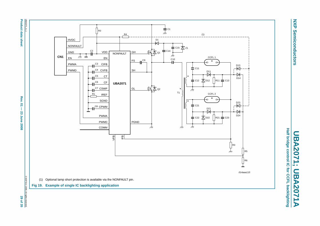
12. Application information
Figure 19 shows an example backlighting configuration, where the inverter is suppliedfrom a high voltage DC source and the IC is supplied by means of a ∆V/∆t supply (C14,C15, Z1 and D1). Two lamps are connected, each to the output of its own transformer. Theleakage inductance of this transformer provides the ballast impedance for the lamps. Ananalog voltage is converted to a PWM signal to provide for the desired brightness level.Lamp short detection is done via the lamp voltage sensing, D13 and D23, and theNONFAULT pin.
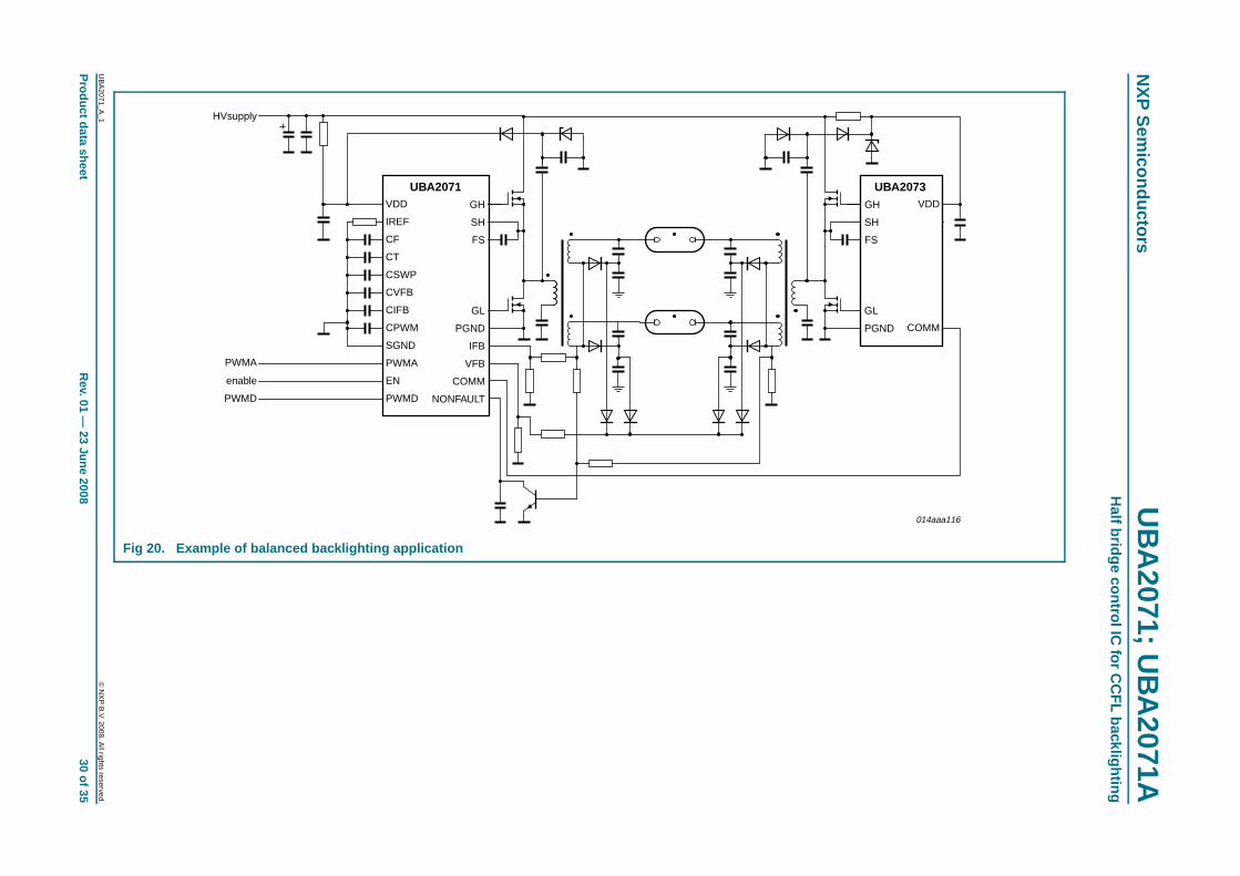
Figure 20 shows an example of a balanced application using one UBA2071 and oneUBA2073.
UBA2071_A_1 © NXP B.V. 2008. All rights reserved.
Product data sheet Rev. 01 — 23 June 2008 28 of 35
xxxxxxxxxxxxxxxxxxxxx xxxxxxxxxxxxxxxxxxxxxxxxxx xxxxxxx x x x xxxxxxxxxxxxxxxxxxxxxxxxxxxxxx xxxxxxxxxxxxxxxxxxx xx xxxxxxx xxxxxxxxxxxxxxxxxxxxxxxxxxx xxxxxxxxxxxxxxxxxxx xxxxxx xxxxxxxxxxxxxxxxxxxxxxxxxxxxxxxxxxx xxxxxxxxxxxx x xxxxxxxxxxxxxxxxxxxxxx xxxxxxxxxxxxxxxxxxxxxxxxxxxxxx xxxxx xxxxxxxxxxxxxxxxxxxxxxxxxxxxxxxxxxxxxxxxxxxxxxxxxx xxxxxxxxxxxxxxxxxxxxxxxxxxxxxxxxx xxxxxxxxxxxxxxxxxxxx xxx
UB
A2071_A
_1
Product data shee
NX
P S
emiconductors
UB
A2071; U
BA
2071AH
alf bridge control IC for C
CF
L backlightingR2
HVDC D1
C1
FL 2
FL 1
R11 C13D14
R21 C23D24
R3
R5
R6
R4
D23
D13
(1)
014aaa115
© N
XP
B.V. 2008. A
ll rights reserved.
tR
ev. 01 — 23 June 2008
29 of 35
(1) Optional lamp short protection is available via the NONFAULT pin.
Fig 19. Example of single IC backlighting application
C2 VDD GH
FS
SH
GL
PGND
EN
C3 CIFB
C4 CVFB
C5 CT
C6 CF
C7 CSWP
IREF
SGND
C8 CPWM
PWMA
PWMD
COMM
PWMD
CN1
UBA2071
PWMA
EN
GND
NONFAULT
C9
Q2
Q1C14
C10
C15 Z1
C12 D12
CC
CC
D11C11
C22 D22
D21C21
IFB
VF
B
NONFAULT
T1R1
xxxxxxxxxxxxxxxxxxxxx xxxxxxxxxxxxxxxxxxxxxxxxxx xxxxxxx x x x xxxxxxxxxxxxxxxxxxxxxxxxxxxxxx xxxxxxxxxxxxxxxxxxx xx xxxxxxx xxxxxxxxxxxxxxxxxxxxxxxxxxx xxxxxxxxxxxxxxxxxxx xxxxxx xxxxxxxxxxxxxxxxxxxxxxxxxxxxxxxxxxx xxxxxxxxxxxx x xxxxxxxxxxxxxxxxxxxxxx xxxxxxxxxxxxxxxxxxxxxxxxxxxxxx xxxxx xxxxxxxxxxxxxxxxxxxxxxxxxxxxxxxxxxxxxxxxxxxxxxxxxx xxxxxxxxxxxxxxxxxxxxxxxxxxxxxxxxx xxxxxxxxxxxxxxxxxxxx xxx
UB
A2071_A
_1
Product data shee
NX
P S
emiconductors
UB
A2071; U
BA
2071AH
alf bridge control IC for C
CF
L backlightingHVsupply
UBA2073VDD
COMM
GL
PGND
GH
SH
FS
014aaa116
© N
XP
B.V. 2008. A
ll rights reserved.
tR
ev. 01 — 23 June 2008
30 of 35
Fig 20. Example of balanced backlighting application
UBA2071VDD
IREF
CF
CT
CSWP
CVFB
CIFB
CPWM
SGND
PWMA
ENenable
PWMDPWMD
GL
PGND
IFB
VFB
COMM
NONFAULT
PWMA
GH
SH
FS
NXP Semiconductors UBA2071; UBA2071AHalf bridge control IC for CCFL backlighting
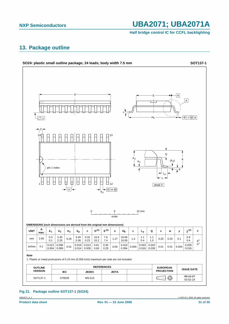
13. Package outline
Fig 21. Package outline SOT137-1 (SO24)
UNITA
max. A1 A2 A3 bp c D (1) E (1) (1)e HE L L p Q Zywv θ
REFERENCESOUTLINEVERSION
EUROPEANPROJECTION ISSUE DATE
IEC JEDEC JEITA
mm
inches
2.65 0.30.1
2.452.25
0.490.36
0.320.23
15.615.2
7.67.4
1.2710.6510.00
1.11.0
0.90.4 8
0
o
o
0.25 0.1
DIMENSIONS (inch dimensions are derived from the original mm dimensions)
Note
1. Plastic or metal protrusions of 0.15 mm (0.006 inch) maximum per side are not included.
1.10.4
SOT137-1
X
12
24
w M
θ
AA1
A2
bp
D
HE
Lp
Q
detail X
E
Z
c
L
v M A
13
(A )3
A
y
0.25
075E05 MS-013
pin 1 index
0.1 0.0120.004
0.0960.089
0.0190.014
0.0130.009
0.610.60
0.300.29
0.05
1.4
0.0550.4190.394
0.0430.039
0.0350.016
0.01
0.25
0.01 0.0040.0430.016
0.01
e
1
0 5 10 mm
scale
SO24: plastic small outline package; 24 leads; body width 7.5 mm SOT137-1
99-12-2703-02-19
UBA2071_A_1 © NXP B.V. 2008. All rights reserved.
Product data sheet Rev. 01 — 23 June 2008 31 of 35
NXP Semiconductors UBA2071; UBA2071AHalf bridge control IC for CCFL backlighting
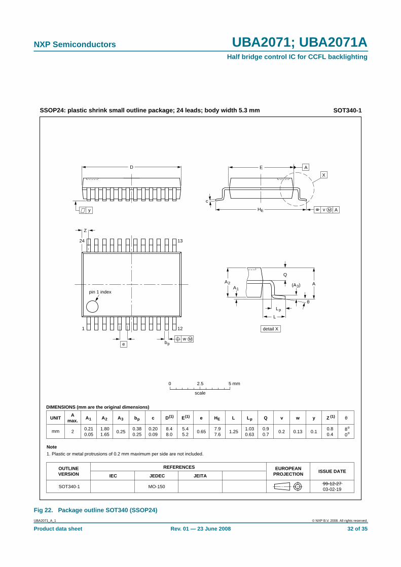
Fig 22. Package outline SOT340 (SSOP24)
UNIT A1 A2 A3 bp c D(1) E(1) (1)e HE L L p Q Zywv θ
REFERENCESOUTLINEVERSION
EUROPEANPROJECTION ISSUE DATE
IEC JEDEC JEITA
mm 0.210.05
1.801.65
0.380.25
0.200.09
8.48.0
5.45.2
0.65 1.257.97.6
0.90.7
0.80.4
80
o
o0.13 0.10.2
DIMENSIONS (mm are the original dimensions)
Note
1. Plastic or metal protrusions of 0.2 mm maximum per side are not included.
1.030.63
SOT340-1 MO-15099-12-2703-02-19
X
w M
θ
AA1
A2
bp
D
HE
Lp
Q
detail X
E
Z
e
c
L
v M A
(A )3
A
1 12
24 13
0.25
y
pin 1 index
0 2.5 5 mm
scale
SSOP24: plastic shrink small outline package; 24 leads; body width 5.3 mm SOT340-1
Amax.
2
UBA2071_A_1 © NXP B.V. 2008. All rights reserved.
Product data sheet Rev. 01 — 23 June 2008 32 of 35
NXP Semiconductors UBA2071; UBA2071AHalf bridge control IC for CCFL backlighting
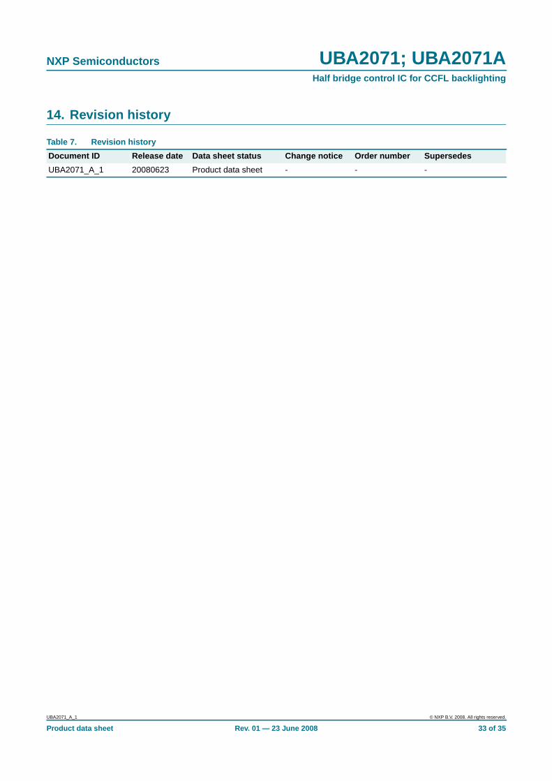
14. Revision history
Table 7. Revision history
Document ID Release date Data sheet status Change notice Order number Supersedes
UBA2071_A_1 20080623 Product data sheet - - -
UBA2071_A_1 © NXP B.V. 2008. All rights reserved.
Product data sheet Rev. 01 — 23 June 2008 33 of 35
NXP Semiconductors UBA2071; UBA2071AHalf bridge control IC for CCFL backlighting
15. Legal information
15.1 Data sheet status
[1] Please consult the most recently issued document before initiating or completing a design.
[2] The term ‘short data sheet’ is explained in section “Definitions”.
[3] The product status of device(s) described in this document may have changed since this document was published and may differ in case of multiple devices. The latest product statusinformation is available on the Internet at URL http://www.nxp.com.
15.2 Definitions
Draft — The document is a draft version only. The content is still underinternal review and subject to formal approval, which may result inmodifications or additions. NXP Semiconductors does not give anyrepresentations or warranties as to the accuracy or completeness ofinformation included herein and shall have no liability for the consequences ofuse of such information.
Short data sheet — A short data sheet is an extract from a full data sheetwith the same product type number(s) and title. A short data sheet is intendedfor quick reference only and should not be relied upon to contain detailed andfull information. For detailed and full information see the relevant full datasheet, which is available on request via the local NXP Semiconductors salesoffice. In case of any inconsistency or conflict with the short data sheet, thefull data sheet shall prevail.
15.3 Disclaimers
General — Information in this document is believed to be accurate andreliable. However, NXP Semiconductors does not give any representations orwarranties, expressed or implied, as to the accuracy or completeness of suchinformation and shall have no liability for the consequences of use of suchinformation.
Right to make changes — NXP Semiconductors reserves the right to makechanges to information published in this document, including withoutlimitation specifications and product descriptions, at any time and withoutnotice. This document supersedes and replaces all information supplied priorto the publication hereof.
Suitability for use — NXP Semiconductors products are not designed,authorized or warranted to be suitable for use in medical, military, aircraft,space or life support equipment, nor in applications where failure ormalfunction of an NXP Semiconductors product can reasonably be expectedto result in personal injury, death or severe property or environmental
damage. NXP Semiconductors accepts no liability for inclusion and/or use ofNXP Semiconductors products in such equipment or applications andtherefore such inclusion and/or use is at the customer’s own risk.
Applications — Applications that are described herein for any of theseproducts are for illustrative purposes only. NXP Semiconductors makes norepresentation or warranty that such applications will be suitable for thespecified use without further testing or modification.
Quick reference data — The Quick reference data is an extract of theproduct data given in the Limiting values and Characteristics sections of thisdocument, and as such is not complete, exhaustive or legally binding.
Limiting values — Stress above one or more limiting values (as defined inthe Absolute Maximum Ratings System of IEC 60134) may cause permanentdamage to the device. Limiting values are stress ratings only and operation ofthe device at these or any other conditions above those given in theCharacteristics sections of this document is not implied. Exposure to limitingvalues for extended periods may affect device reliability.
Terms and conditions of sale — NXP Semiconductors products are soldsubject to the general terms and conditions of commercial sale, as publishedat http://www.nxp.com/profile/terms, including those pertaining to warranty,intellectual property rights infringement and limitation of liability, unlessexplicitly otherwise agreed to in writing by NXP Semiconductors. In case ofany inconsistency or conflict between information in this document and suchterms and conditions, the latter will prevail.
No offer to sell or license — Nothing in this document may be interpretedor construed as an offer to sell products that is open for acceptance or thegrant, conveyance or implication of any license under any copyrights, patentsor other industrial or intellectual property rights.
15.4 TrademarksNotice: All referenced brands, product names, service names and trademarksare the property of their respective owners.
16. Contact information
For more information, please visit: http://www .nxp.com
For sales office addresses, please send an email to: salesad [email protected]
Document status [1] [2] Product status [3] Definition
Objective [short] data sheet Development This document contains data from the objective specification for product development.
Preliminary [short] data sheet Qualification This document contains data from the preliminary specification.
Product [short] data sheet Production This document contains the product specification.
UBA2071_A_1 © NXP B.V. 2008. All rights reserved.
Product data sheet Rev. 01 — 23 June 2008 34 of 35
NXP Semiconductors UBA2071; UBA2071AHalf bridge control IC for CCFL backlighting
17. Contents
1 General description . . . . . . . . . . . . . . . . . . . . . . 12 Features . . . . . . . . . . . . . . . . . . . . . . . . . . . . . . . 13 Applications . . . . . . . . . . . . . . . . . . . . . . . . . . . . 24 Quick reference data . . . . . . . . . . . . . . . . . . . . . 25 Ordering information . . . . . . . . . . . . . . . . . . . . . 36 Block diagram . . . . . . . . . . . . . . . . . . . . . . . . . . 47 Pinning information . . . . . . . . . . . . . . . . . . . . . . 57.1 Pinning . . . . . . . . . . . . . . . . . . . . . . . . . . . . . . . 57.2 Pin description . . . . . . . . . . . . . . . . . . . . . . . . . 58 Functional description . . . . . . . . . . . . . . . . . . . 68.1 Supply, Start-up and UnderVoltage LockOut
(UVLO) . . . . . . . . . . . . . . . . . . . . . . . . . . . . . . . 78.2 VDD clamp. . . . . . . . . . . . . . . . . . . . . . . . . . . . . 88.3 Enable. . . . . . . . . . . . . . . . . . . . . . . . . . . . . . . . 88.4 The oscillator . . . . . . . . . . . . . . . . . . . . . . . . . . 88.5 Non-overlap . . . . . . . . . . . . . . . . . . . . . . . . . . . 98.6 Low-side and high-side drivers . . . . . . . . . . . . . 98.7 DC blocking capacitor charging . . . . . . . . . . . . 98.8 Lamp (re-)ignition . . . . . . . . . . . . . . . . . . . . . . 118.9 Overvoltage control. . . . . . . . . . . . . . . . . . . . . 138.10 Lamp current control. . . . . . . . . . . . . . . . . . . . 148.11 PWM dimming . . . . . . . . . . . . . . . . . . . . . . . . 158.12 The fault timer. . . . . . . . . . . . . . . . . . . . . . . . . 178.13 Communication. . . . . . . . . . . . . . . . . . . . . . . . 188.14 Protections . . . . . . . . . . . . . . . . . . . . . . . . . . . 188.14.1 Voltage feedback open or short protection . . . 198.14.2 Overvoltage protection . . . . . . . . . . . . . . . . . . 208.14.3 Hard switching protection . . . . . . . . . . . . . . . . 208.14.4 Overvoltage extra protection. . . . . . . . . . . . . . 208.14.5 Current feedback open or short protection . . . 218.14.6 Overcurrent detection . . . . . . . . . . . . . . . . . . . 218.14.7 Arcing detection . . . . . . . . . . . . . . . . . . . . . . . 218.14.8 Ignition Failure (IF) . . . . . . . . . . . . . . . . . . . . . 228.14.9 The NONFAULT pin . . . . . . . . . . . . . . . . . . . . 228.14.10 Fault input via the COMM pin . . . . . . . . . . . . . 239 Limiting values. . . . . . . . . . . . . . . . . . . . . . . . . 2310 Thermal characteristics. . . . . . . . . . . . . . . . . . 2411 Characteristics . . . . . . . . . . . . . . . . . . . . . . . . . 2412 Application information. . . . . . . . . . . . . . . . . . 2813 Package outline . . . . . . . . . . . . . . . . . . . . . . . . 3114 Revision history . . . . . . . . . . . . . . . . . . . . . . . . 3315 Legal information. . . . . . . . . . . . . . . . . . . . . . . 3415.1 Data sheet status . . . . . . . . . . . . . . . . . . . . . . 3415.2 Definitions . . . . . . . . . . . . . . . . . . . . . . . . . . . . 3415.3 Disclaimers . . . . . . . . . . . . . . . . . . . . . . . . . . . 34
15.4 Trademarks . . . . . . . . . . . . . . . . . . . . . . . . . . 3416 Contact information . . . . . . . . . . . . . . . . . . . . 3417 Contents. . . . . . . . . . . . . . . . . . . . . . . . . . . . . . 35
© NXP B.V. 2008. All rights reserved.For more information, please visit: http://www.nxp.comFor sales office addresses, please send an email to: [email protected]
Date of release: 23 June 2008
Document identifier: UBA2071_A_1
Please be aware that important notices concerning this document and the product(s)described herein, have been included in section ‘Legal information’.