Embed Size (px)
Citation preview

Understanding Operational Amplifiers
Cheng Zhang
Nan Xia
Alexander Gollin
Kenneth Young
Patrick Powers

Outline
• Cheng - History
• Pat - OP AMP Construction/design
• Alex - OP Amp Application Circuits
• Ken - Effect of Input offset voltage
• Nan - Effect of Slew Rate, Packaging, Conclusion

1941 First vacuum tube op-amp Karl D. Swartzel Jr.
1947 First op-amp with non-inverting input
John R. Ragazzini
1949 First chopper-stabilized op-amp
Edwin A. Goldberg
1961 Discrete IC op-amp
History

1963 First monolithic IC op-amp Bob Widlar
1970 First high-speed, low-input current FET design
1972 Single sided supply op-amps being produced
History Continued

Op Amp Construction
• Integrated Circuit(IC) Main Categories: • Linear ICs
• Performs amplification or linear operations on signals.
• Monolithic (“one stone”) Circuits • The entire circuit is embedded upon a single piece of
semiconductor.

μA741 Op-Amp
•Bias Circuit
•Input Stage
•Intermediate Stage
•Output Stage
•Short-circuit Protection
Internal Schematic from LM741 Datasheet

Monolithic Building Blocks

Biasing Circuit

Biasing Circuit

Input Stage

Input Stage
• Q1, Q2 are emitter followers.
• Q3, Q4 in common-base configuration serve as differential amplifier, level shifters and protect Q1, Q2 against emitter-base junction breakdown.
• Q5, Q6, Q7 and R1, R2, R3 provide the load (active load) for the differential amplifier.
Intermediate Stage

Intermediate Stage
• Q16 is an emitter follower.
• Q17 is a common-emitter amplifier, loaded by Q13B.
• GAIN≈ (gm-Q17)( r0-Q13B)
• Cc is the internal compensation cap used to maintain stability when the op-amp is used in a feedback configuration.

Output Stage

Output Stage
• Q23 is an emitter follower.
• Q14, Q20 are a complementary push-pull, or Class AB amplifier.
• Q19, Q18 are a Darlington-pair, but act similar to diodes. They maintain a VBE drop to smooth out the crossover distortion of Q14, Q20.
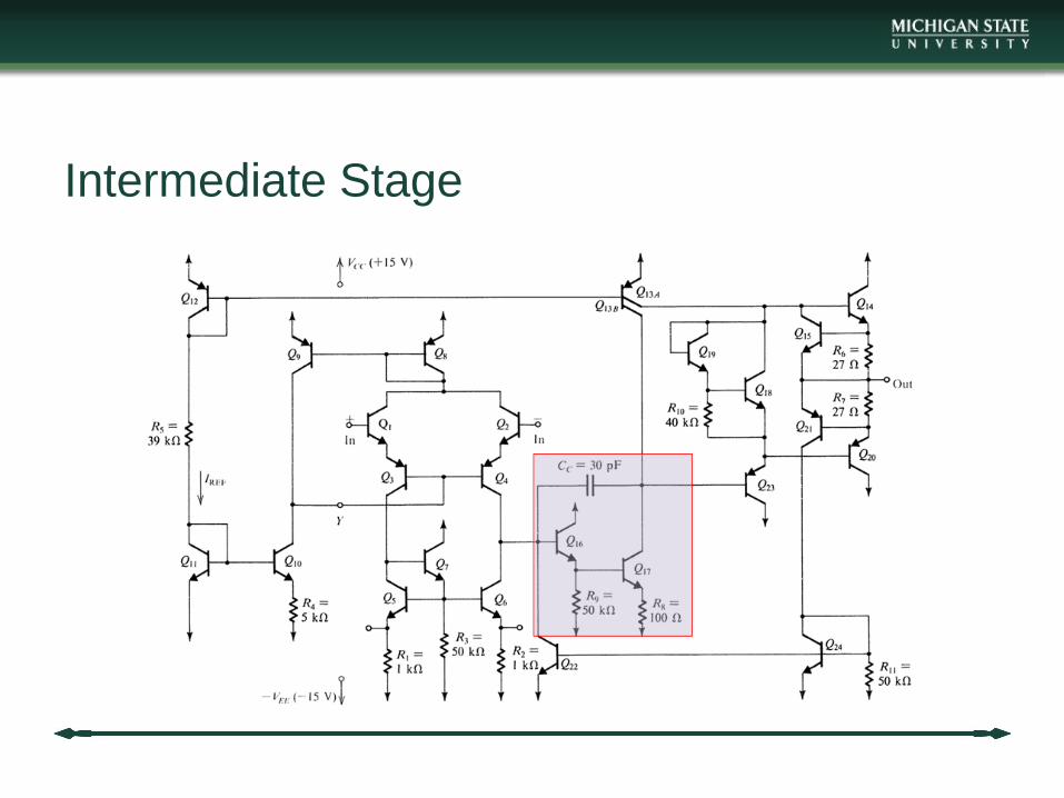
Short-circuit Protection

Short-circuit Protection
• Q15, Q21 are normally off.
• If too much current is being output (~25mA), the voltage drop across R6, R7 will turn Q15, Q21 on to bleed off the current via Q22, Q24 current mirror.

Op-amp Design Applications
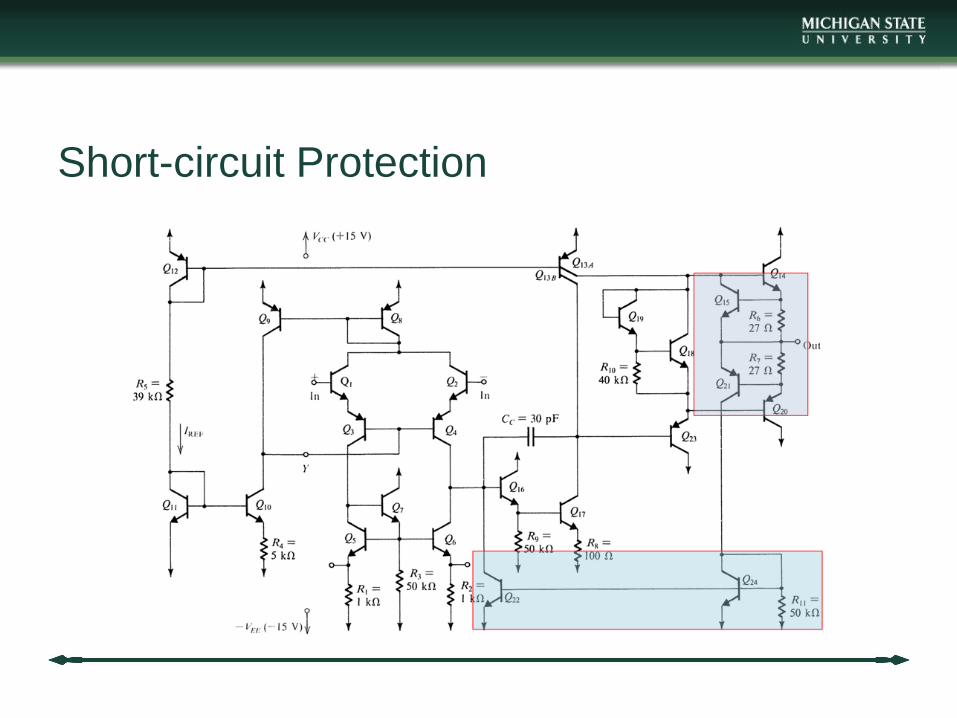
Simple Buffer Circuit
or Voltage Follower Typical 8-pin Op-Amp Layout
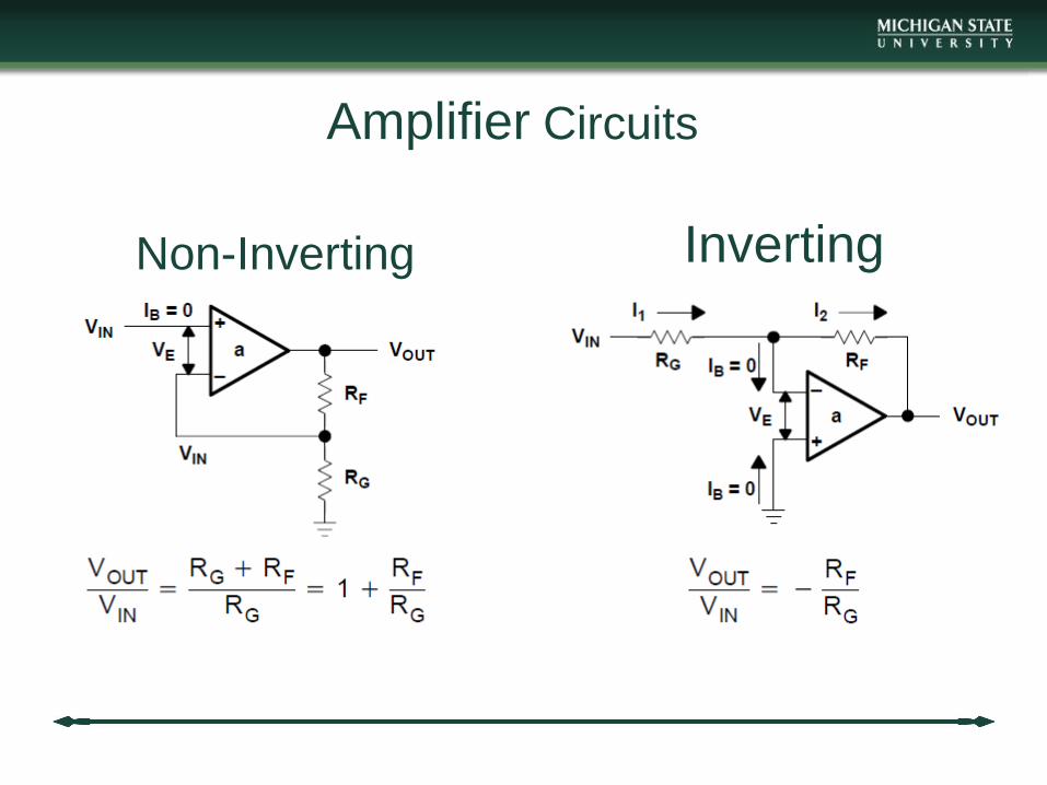
Inverting Non-Inverting
Amplifier Circuits

Differential Adder

Non-Inverting Summing Amplifier

Integrator

Active Filter Design
Active Passive

OP AMP Specifications
Some Specifications to be aware of when using Operational Amplifiers in your circuits.
• Input Offset Voltage- Input Offset Null Pins
• Slew Rate

LM741 Datasheet


What is Input Offset Voltage?
In an Ideal Op Amp the
output should be exactly 0v
with inputs shorted.
However In a real OP Amp
there will be some output
voltage when the inputs are
shorted due to slight
differences in the internal
OP Amp transistors
Ideal OP AMP
Real OP AMP

What Causes Input Offset Voltage?
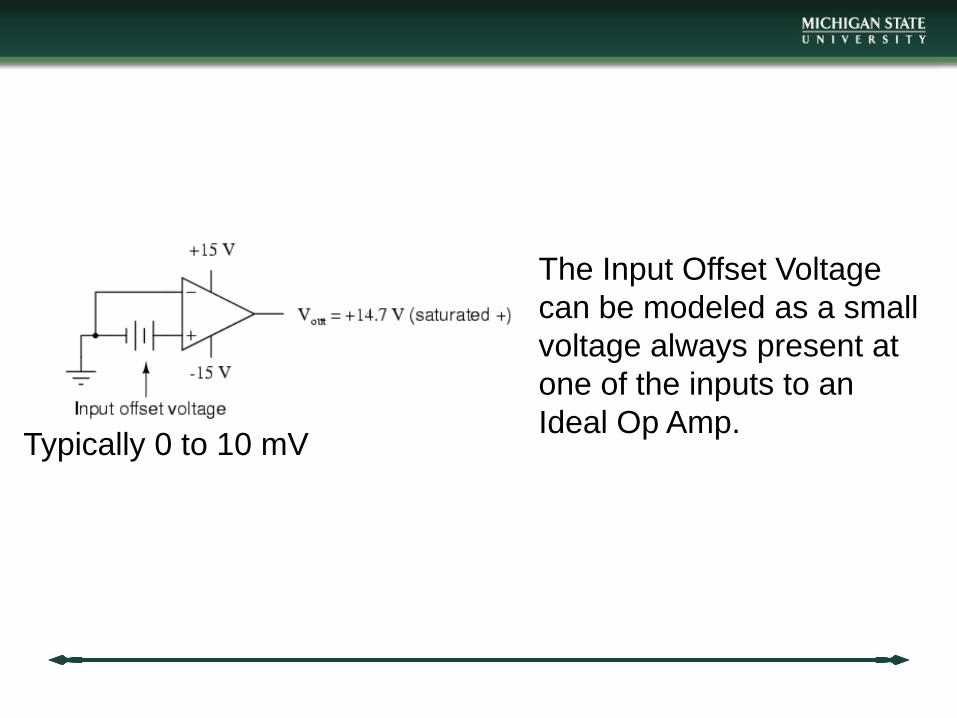
The Input Offset Voltage
can be modeled as a small
voltage always present at
one of the inputs to an
Ideal Op Amp. Typically 0 to 10 mV

Effect of Input Offset Voltage

LM741 Null Pins
Some Op Amps have NULL Pins which allow adjustment to compensate for Input Offset Voltage.
• LM741 Has Null Pins
• LM324 Does NOT have Null Pins
LM741

LM741 Schematic
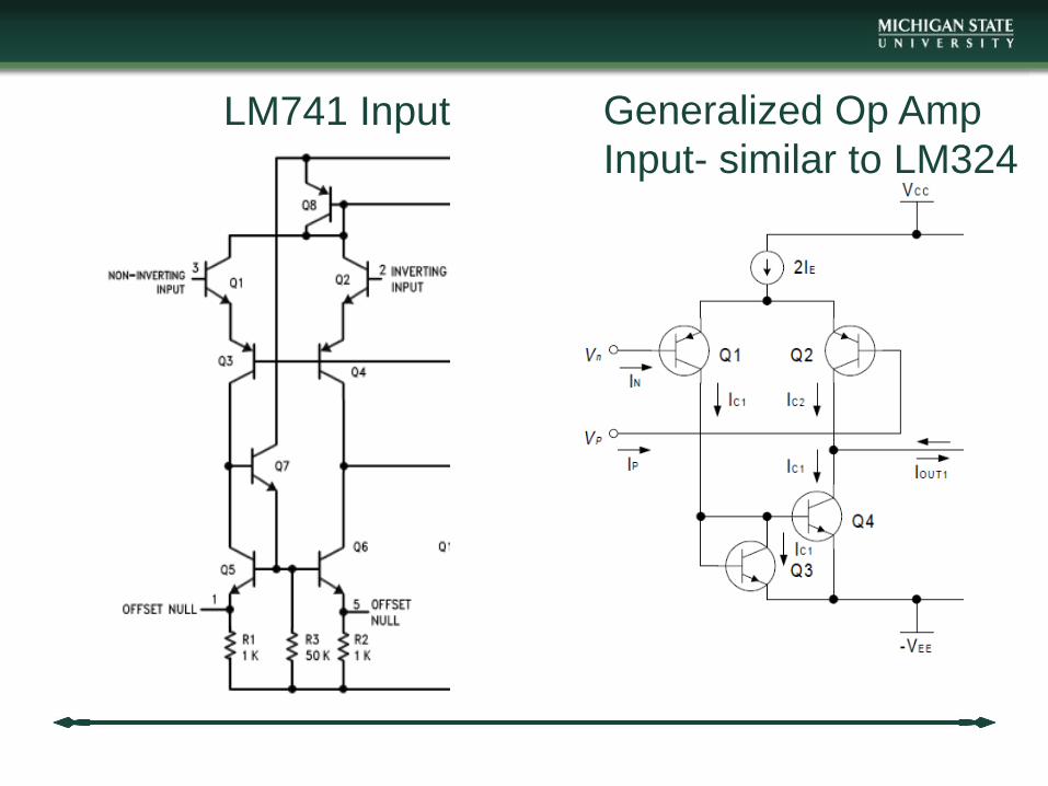
LM741 Input Generalized Op Amp
Input- similar to LM324

LM741 Input

Slew Rate The Slew Rate of an Op Amp is the maximum rate of change in the output voltage expressed in volts/µs
The LM741 has a slew rate of 0.5 volts/µs
Input
Output
0.5 volts/µs

Input
Output
0.5 volts/µs

Purchasing an Op-amp
• Package • DIP • TSSOP • MSOP
• Mount Type • Surface Mount • Through Hole

1. Package
• Dual in-line-package (DIP):
Regular sized op amp.
• Thin Shrink Small outline package (TSSOP):
Smaller body size & lead pitches (0.9mm thick).
• Micro small outline package (MSOP):
Only 3mm * 3mm body.

2. Mount type
• Surface mount
SOPs are surface mount. Need sockets to solder on the PCB.
• Through hole
DIPs are though hole. Sockets will help to remove or switch the op amp.

Conclusion
Cheng - History Pat - OP AMP Construction/design Alex - OP Amp Application Circuits Ken - Effect of Input offset voltage Nan - Effect of Slew Rate, Packaging, Conclusion

Thank you