Embed Size (px)
Citation preview
An IC Operational Transconducta
AN6077 Rev 3.00Oct 2000
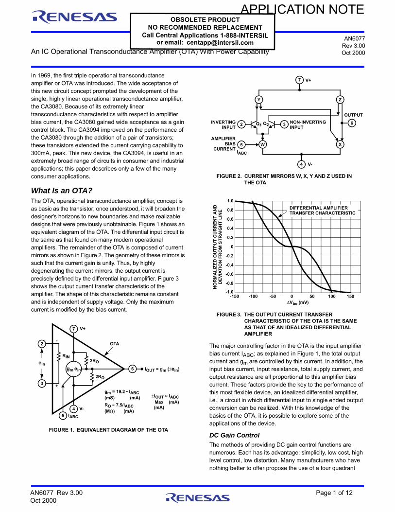
APPLICATION NOTE
AN6077
OBSOLETE PRODUCTNO RECOMMENDED REPLACEMENT
Call Central Applications 1-888-INTERSIL
nce Amplifier (OTA) With Power CapabilityRev 3.00Oct 2000
October 2000or email: [email protected]
In 1969, the first triple operational transconductance amplifier or OTA was introduced. The wide acceptance of this new circuit concept prompted the development of the single, highly linear operational transconductance amplifier, the CA3080. Because of its extremely linear transconductance characteristics with respect to amplifier bias current, the CA3080 gained wide acceptance as a gain control block. The CA3094 improved on the performance of the CA3080 through the addition of a pair of transistors; these transistors extended the current carrying capability to 300mA, peak. This new device, the CA3094, is useful in an extremely broad range of circuits in consumer and industrial applications; this paper describes only a few of the many consumer applications.
What Is an OTA?The OTA, operational transconductance amplifier, concept is as basic as the transistor; once understood, it will broaden the designer's horizons to new boundaries and make realizable designs that were previously unobtainable. Figure 1 shows an equivalent diagram of the OTA. The differential input circuit is the same as that found on many modern operational amplifiers. The remainder of the OTA is composed of current mirrors as shown in Figure 2. The geometry of these mirrors is such that the current gain is unity. Thus, by highly degenerating the current mirrors, the output current is precisely defined by the differential input amplifier. Figure 3 shows the output current transfer characteristic of the amplifier. The shape of this characteristic remains constant and is independent of supply voltage. Only the maximum current is modified by the bias current.
The major controlling factor in the OTA is the input amplifier bias current IABC; as explained in Figure 1, the total output current and gm are controlled by this current. In addition, the input bias current, input resistance, total supply current, and output resistance are all proportional to this amplifier bias current. These factors provide the key to the performance of this most flexible device, an idealized differential amplifier, i.e., a circuit in which differential input to single ended output conversion can be realized. With this knowledge of the basics of the OTA, it is possible to explore some of the applications of the device.
DC Gain Control
The methods of providing DC gain control functions are numerous. Each has its advantage: simplicity, low cost, high level control, low distortion. Many manufacturers who have nothing better to offer propose the use of a four quadrant
RIN
OTA
2RO
IABC
ein
V+
V-
2RO
+
-
6
4
5
7
gm ein
2
3
IOUT = gm (ein)
gm =(mS)
19.2 • IABC(mA)
RO 7.5/IABC(M) (mA)
IOUT IABCMax(mA)
(mA)
FIGURE 1. EQUIVALENT DIAGRAM OF THE OTA
Y
W X
Z
4
6
OUTPUT
3 NON-INVERTINGINPUT
2INVERTINGINPUT
Q1 Q2
5AMPLIFIER
BIASCURRENT
IABC
7
V-
V+
FIGURE 2. CURRENT MIRRORS W, X, Y AND Z USED INTHE OTA
DIFFERENTIAL AMPLIFIERTRANSFER CHARACTERISTIC
Vbe (mV)
NO
RM
AL
IZE
D O
UT
PU
T C
UR
RE
NT
AN
DD
EV
IAT
ION
FR
OM
ST
RA
IGH
T L
INE
1.0
0.8
0.6
0.4
0.2
0
-0.2
-0.4
-0.6
-0.8
-1.0-150 -100 -50 0 50 100 150
FIGURE 3. THE OUTPUT CURRENT TRANSFER CHARACTERISTIC OF THE OTA IS THE SAME AS THAT OF AN IDEALIZED DIFFERENTIAL AMPLIFIER
Page 1 of 12
An IC Operational Transconductance
Amplifier (OTA) With Power Capability
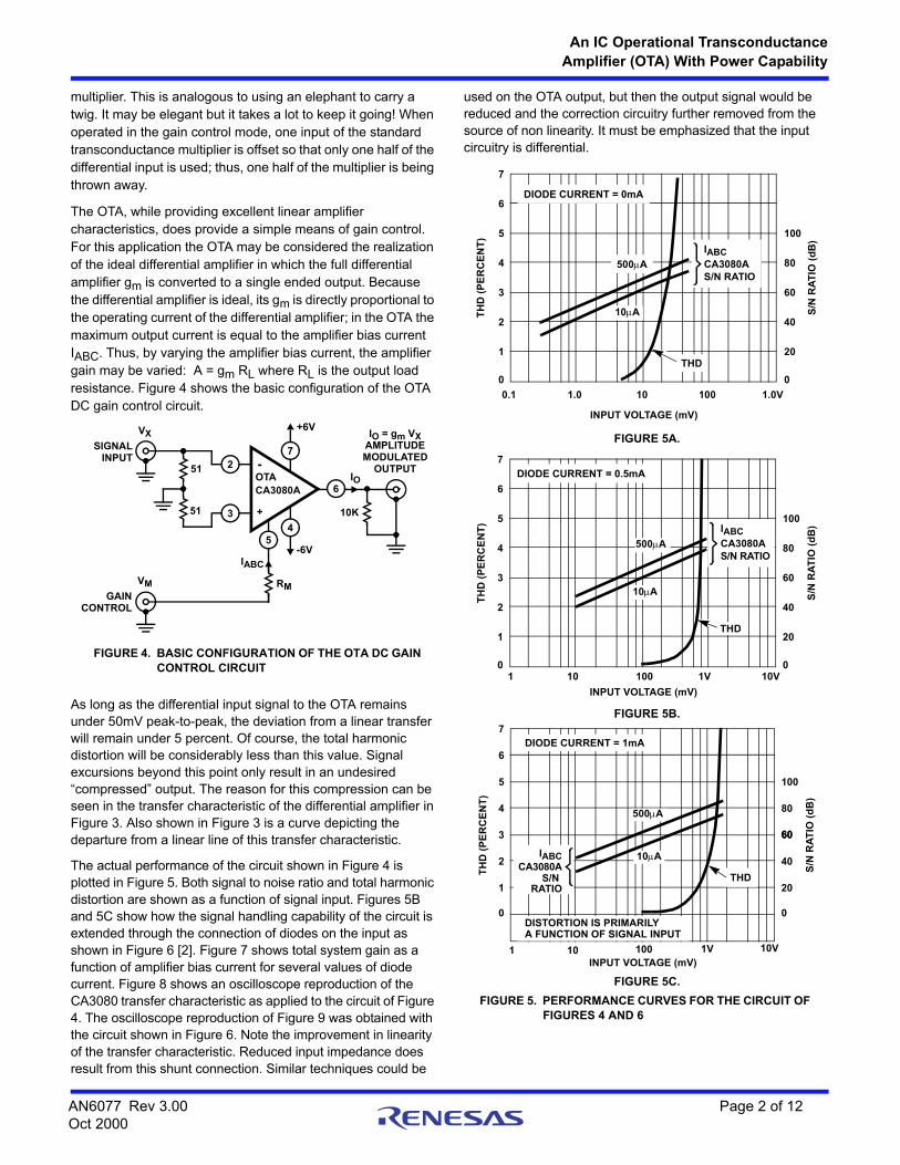
multiplier. This is analogous to using an elephant to carry a twig. It may be elegant but it takes a lot to keep it going! When operated in the gain control mode, one input of the standard transconductance multiplier is offset so that only one half of the differential input is used; thus, one half of the multiplier is being thrown away.
The OTA, while providing excellent linear amplifier characteristics, does provide a simple means of gain control. For this application the OTA may be considered the realization of the ideal differential amplifier in which the full differential amplifier gm is converted to a single ended output. Because the differential amplifier is ideal, its gm is directly proportional to the operating current of the differential amplifier; in the OTA the maximum output current is equal to the amplifier bias current IABC. Thus, by varying the amplifier bias current, the amplifier gain may be varied: A = gm RL where RL is the output load resistance. Figure 4 shows the basic configuration of the OTA DC gain control circuit.
As long as the differential input signal to the OTA remains under 50mV peak-to-peak, the deviation from a linear transfer will remain under 5 percent. Of course, the total harmonic distortion will be considerably less than this value. Signal excursions beyond this point only result in an undesired “compressed” output. The reason for this compression can be seen in the transfer characteristic of the differential amplifier in Figure 3. Also shown in Figure 3 is a curve depicting the departure from a linear line of this transfer characteristic.
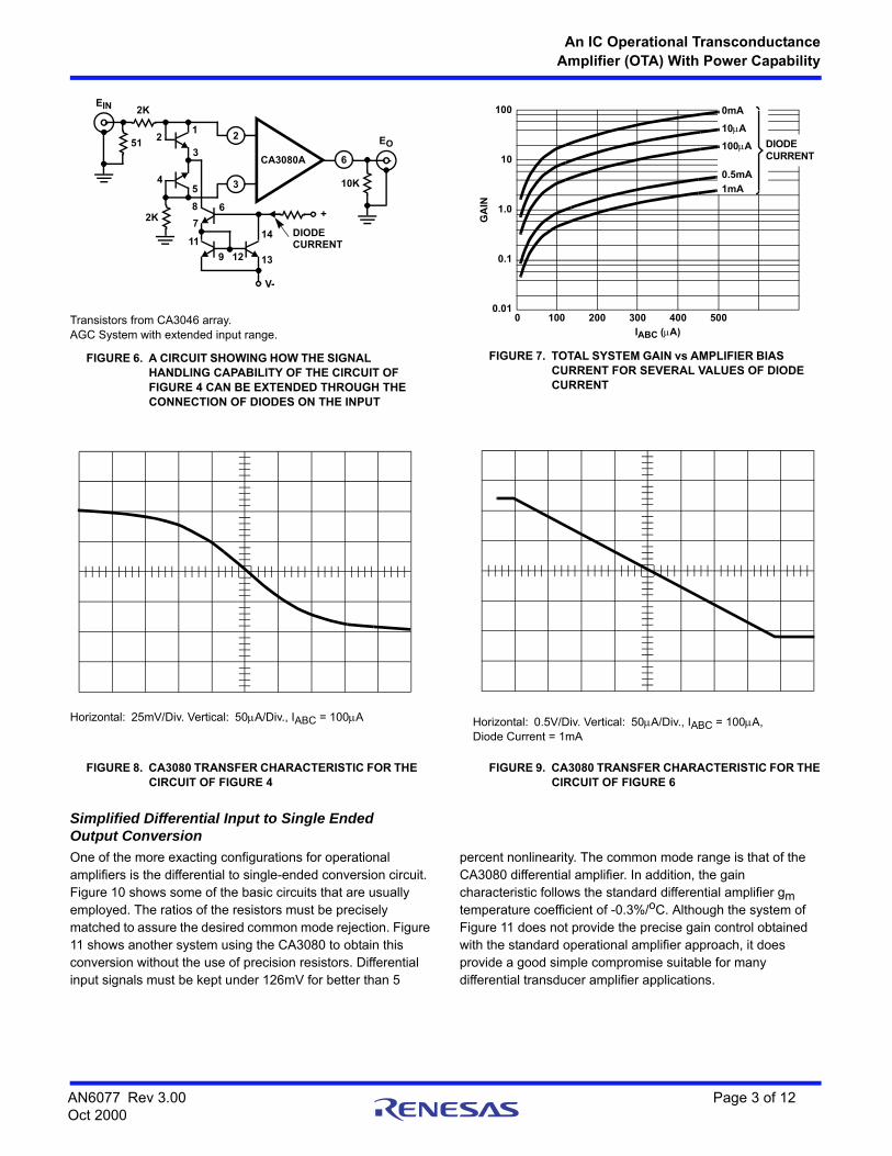
The actual performance of the circuit shown in Figure 4 is plotted in Figure 5. Both signal to noise ratio and total harmonic distortion are shown as a function of signal input. Figures 5B and 5C show how the signal handling capability of the circuit is extended through the connection of diodes on the input as shown in Figure 6 [2]. Figure 7 shows total system gain as a function of amplifier bias current for several values of diode current. Figure 8 shows an oscilloscope reproduction of the CA3080 transfer characteristic as applied to the circuit of Figure 4. The oscilloscope reproduction of Figure 9 was obtained with the circuit shown in Figure 6. Note the improvement in linearity of the transfer characteristic. Reduced input impedance does result from this shunt connection. Similar techniques could be
used on the OTA output, but then the output signal would be reduced and the correction circuitry further removed from the source of non linearity. It must be emphasized that the input circuitry is differential.
3
54
7
OTACA3080A
251
51 +
-
6
SIGNALINPUT
VX
VMGAIN
CONTROL
IABC
RM
-6V
+6V
10K
IO
IO = gm VXAMPLITUDEMODULATED
OUTPUT
FIGURE 4. BASIC CONFIGURATION OF THE OTA DC GAIN CONTROL CIRCUIT
FIGURE 5A.
FIGURE 5B.
FIGURE 5C.
FIGURE 5. PERFORMANCE CURVES FOR THE CIRCUIT OF FIGURES 4 AND 6
7
6
5
4
3
2
1
0
0.1 1.0 10 100 1.0V
INPUT VOLTAGE (mV)
TH
D (
PE
RC
EN
T) 100
80
60
40
20
0
S/N
RA
TIO
(d
B)
THD
DIODE CURRENT = 0mA
500A
10A
IABCCA3080AS/N RATIO
7
6
5
4
3
2
1
01 10 100 1V 10V
INPUT VOLTAGE (mV)
TH
D (
PE
RC
EN
T) 100
80
60
40
20
0
S/N
RA
TIO
(d
B)
THD
DIODE CURRENT = 0.5mA
IABCCA3080AS/N RATIO
500A
10A
7
6
5
4
3
2
1
0
1 10 100 1V 10V
INPUT VOLTAGE (mV)
TH
D (
PE
RC
EN
T)
100
80
60
40
20
0
S/N
RA
TIO
(d
B)
THD
DIODE CURRENT = 1mA
IABCCA3080A
S/N
500A
10A
RATIO
DISTORTION IS PRIMARILYA FUNCTION OF SIGNAL INPUT
60
AN6077 Rev 3.00 Page 2 of 12Oct 2000
An IC Operational Transconductance
Amplifier (OTA) With Power Capability
Simplified Differential Input to Single EndedOutput Conversion
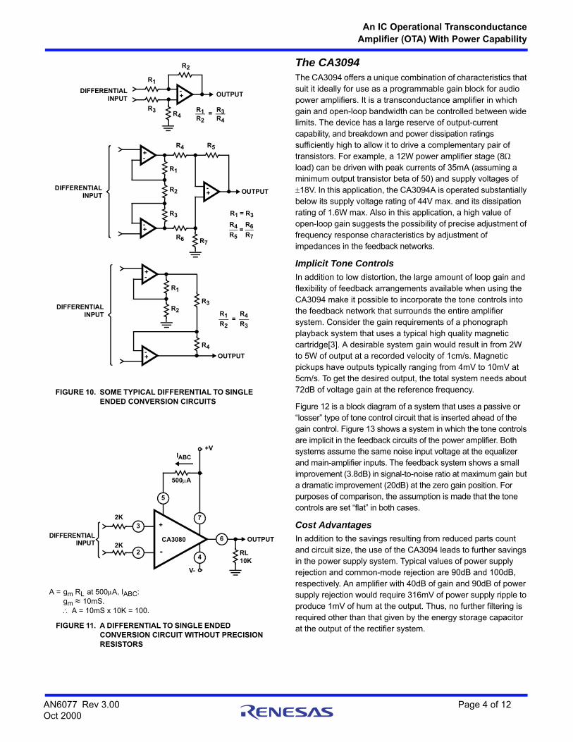
One of the more exacting configurations for operational amplifiers is the differential to single-ended conversion circuit. Figure 10 shows some of the basic circuits that are usually employed. The ratios of the resistors must be precisely matched to assure the desired common mode rejection. Figure 11 shows another system using the CA3080 to obtain this conversion without the use of precision resistors. Differential input signals must be kept under 126mV for better than 5
percent nonlinearity. The common mode range is that of the CA3080 differential amplifier. In addition, the gain characteristic follows the standard differential amplifier gm temperature coefficient of -0.3%/oC. Although the system of Figure 11 does not provide the precise gain control obtained with the standard operational amplifier approach, it does provide a good simple compromise suitable for many differential transducer amplifier applications.
Transistors from CA3046 array.AGC System with extended input range.
FIGURE 6. A CIRCUIT SHOWING HOW THE SIGNAL HANDLING CAPABILITY OF THE CIRCUIT OF FIGURE 4 CAN BE EXTENDED THROUGH THE CONNECTION OF DIODES ON THE INPUT
FIGURE 7. TOTAL SYSTEM GAIN vs AMPLIFIER BIAS CURRENT FOR SEVERAL VALUES OF DIODE CURRENT
FIGURE 8. CA3080 TRANSFER CHARACTERISTIC FOR THE CIRCUIT OF FIGURE 4
FIGURE 9. CA3080 TRANSFER CHARACTERISTIC FOR THE CIRCUIT OF FIGURE 6
3
CA3080A
251
2K
6
DIODECURRENT
10K
EO
EIN
2K +
V-
12
3
45
6
7
8
9
11
12 13
14
0mA
10A
100A
1mA
0.5mA
IABC (A)
0 100 200 300 400 500
100
10
1.0
0.1
0.01
GA
IN
DIODECURRENT
Horizontal: 25mV/Div. Vertical: 50A/Div., IABC = 100A Horizontal: 0.5V/Div. Vertical: 50A/Div., IABC = 100A,Diode Current = 1mA
AN6077 Rev 3.00 Page 3 of 12Oct 2000
An IC Operational Transconductance
Amplifier (OTA) With Power Capability
The CA3094The CA3094 offers a unique combination of characteristics that suit it ideally for use as a programmable gain block for audio power amplifiers. It is a transconductance amplifier in which gain and open-loop bandwidth can be controlled between wide limits. The device has a large reserve of output-current capability, and breakdown and power dissipation ratings sufficiently high to allow it to drive a complementary pair of transistors. For example, a 12W power amplifier stage (8 load) can be driven with peak currents of 35mA (assuming a minimum output transistor beta of 50) and supply voltages of 18V. In this application, the CA3094A is operated substantially below its supply voltage rating of 44V max. and its dissipation rating of 1.6W max. Also in this application, a high value of open-loop gain suggests the possibility of precise adjustment of frequency response characteristics by adjustment of impedances in the feedback networks.
Implicit Tone Controls
In addition to low distortion, the large amount of loop gain and flexibility of feedback arrangements available when using the CA3094 make it possible to incorporate the tone controls into the feedback network that surrounds the entire amplifier system. Consider the gain requirements of a phonograph playback system that uses a typical high quality magnetic cartridge[3]. A desirable system gain would result in from 2W to 5W of output at a recorded velocity of 1cm/s. Magnetic pickups have outputs typically ranging from 4mV to 10mV at 5cm/s. To get the desired output, the total system needs about 72dB of voltage gain at the reference frequency.
Figure 12 is a block diagram of a system that uses a passive or “losser” type of tone control circuit that is inserted ahead of the gain control. Figure 13 shows a system in which the tone controls are implicit in the feedback circuits of the power amplifier. Both systems assume the same noise input voltage at the equalizer and main-amplifier inputs. The feedback system shows a small improvement (3.8dB) in signal-to-noise ratio at maximum gain but a dramatic improvement (20dB) at the zero gain position. For purposes of comparison, the assumption is made that the tone controls are set “flat” in both cases.
Cost Advantages
In addition to the savings resulting from reduced parts count and circuit size, the use of the CA3094 leads to further savings in the power supply system. Typical values of power supply rejection and common-mode rejection are 90dB and 100dB, respectively. An amplifier with 40dB of gain and 90dB of power supply rejection would require 316mV of power supply ripple to produce 1mV of hum at the output. Thus, no further filtering is required other than that given by the energy storage capacitor at the output of the rectifier system.
R2
+-
R1
R3 R4
OUTPUTDIFFERENTIALINPUT
R1R2
=R3R4
R5
+-
R4
R7
OUTPUTDIFFERENTIALINPUT
R4
R5=
R6
R7
R1
+-
R2
R3
+-
R6
R1 = R3
OUTPUT
DIFFERENTIALINPUT
R1
+-
R2
+-
R3
R4
R1
R2=
R4
R3
FIGURE 10. SOME TYPICAL DIFFERENTIAL TO SINGLE ENDED CONVERSION CIRCUITS
24
CA3080
37
5
-
+
V-
2K
62K
10KRL
OUTPUT
+VIABC
500A
A = gm RL at 500A, IABC:gm 10mS. A = 10mS x 10K = 100.
FIGURE 11. A DIFFERENTIAL TO SINGLE ENDED CONVERSION CIRCUIT WITHOUT PRECISION RESISTORS
DIFFERENTIALINPUT
AN6077 Rev 3.00 Page 4 of 12Oct 2000
An IC Operational Transconductance
Amplifier (OTA) With Power Capability
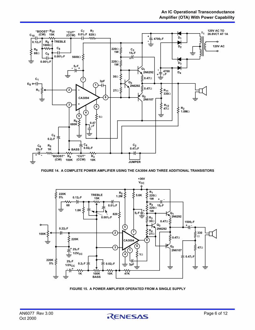
Power Amplifier Using the CA3094A complete power amplifier using the CA3094 and three additional transistors is shown schematically in Figure 14. The amplifier is shown in a single-channel configuration, but power supply values are designed to support a minimum of two channels. The output section comprises Q1 and Q2, complementary epitaxial units connected in the familiar “bootstrap” arrangement. Capacitor C3 provides added base drive for Q1 during positive excursions of the output. The circuit can be operated from a single power supply as well as from a split supply as shown in Figure 15. The changes required for 14.4V operation with a 3.2 speaker are also indicated in the diagram.
The amplifier may also be modified to accept input from ceramic phonograph cartridges. For standard inputs (equalizer preamplifiers, tuners, etc.) C1 is 0.047F, R1 is 250k, and R2 and C2 are omitted. For ceramic-cartridge inputs, C1 is 0.0047F, R1 is 2.5M, and the jumper across C2 is removed.
Output BiasingInstead of the usual two-diode arrangement for establishing idling currents in Q1 and Q2, a “Vbe Multiplier”, transistor Q3, is used. This method of biasing establishes the voltage between the base of Q1 and the base of Q2 at a constant multiple of the base to emitter voltage of a single transistor while maintaining a low variational impedance between its collector and emitter (see Appendix A). If transistor Q3 is mounted in intimate thermal contact with the output units, the operating temperature of the heat sink forces the Vbe of Q3 up and down inversely with heat-sink temperature. The voltage bias between the bases of Q1 and Q2 varies inversely with heat sink temperature and tends to keep the idling current in Q1 and Q2 constant.
A bias arrangement that can be accomplished at lower cost than those already described replaces the Vbe multiplier with a 1N5391 diode in series with an 8.2 resistor. This arrangement does not provide the degree of bias stability of the Vbe multiplier, but is adequate for many applications.
Tone-ControlsThe tone controls, the essential elements of the feedback system, are located in two sets of parallel paths. The bass network includes R3, R4, R5, C4, and C5. C6 blocks the DC from the feedback network so that the DC gain from input to the feedback takeoff point is unity. The residual DC output voltage at the speaker terminals is then
where R1 is the source resistance. The input bias current is then
The treble network consists of R7, R8, R9, R10, C7, C8, C9, and C10. Resistors R7 and R9 limit the maximum available cut and boost, respectively. The boost limit is useful in curtailing heating due to finite turn-off time in the output units. The limit is also desirable when there are tape recorders nearby. The cut limit aids the stability of the amplifier by cutting the loop gain at higher frequencies where phase shifts become significant.
In cases in which absolute stability under all load conditions is required, it may be necessary to insert a small inductor in the output lead to isolate the circuit from capacitive loads. A 3H inductor (1A) in parallel with a 22 resistor is adequate. The derivation of circuit constants is shown in Appendix B. Curves of control action versus electrical rotation are also given.
FIGURE 12. BLOCK DIAGRAM OF A SYSTEM USING A “LOSSER” TYPE TONE CONTROL CIRCUIT
FIGURE 13. A SYSTEM IN WHICH TONE CONTROLS ARE IMPLICIT IN THE FEEDBACK CIRCUIT OF THE POWER AMPLIFIER
EQUALIZERAREF = 32dB
EN AT INPUT = 1 x 10⁻⁶
TONECONTROLS
-20dB
VOLUMECONTROLS
POWERAMP
PICKUPESIG =1mV
BUFFER STAGEEN AT INPUT = 5 x 10⁻⁶
EN = 6.23 x 10⁻³EN = 4 x 10⁻⁶EN = 4 x 10⁻⁶EN = 40 x 10-6
ESIG = 40mV ESIG = 4mV ESIG = 4mVATOTAL = 60dB
8SPEAKER
TOTAL GAIN = 72dB
EO
EN
4
6.23 x 10-3= = 640 AT MAX VOL
EN = 4mV AT MIN VOL
EO = 4V
EQUALIZERAREF = 32dB
EN AT INPUT = 1 x 10⁻⁶
VOLUMECONTROLS
AMPLIFIER WITH FEED-
EN = 5 x 10⁻⁶
EN = 4.03 x 10⁻³
ESIG = 40mV ESIG = 40mVATOTAL = 60dB
EO
EN
4
4.03 x 10-3= = 990 AT MAX VOL
EN = 0.5mV AT MIN VOL
EO = 4V
EN = 40 x 10-6 EN = 40 x 10-6
PICKUPESIG =1mV
BACK TONE CONTROLS
R1
R11 R12+
R12---------------------------
IABC
IABC2-------------
VCC VBE–
2R6----------------------------------–=
AN6077 Rev 3.00 Page 5 of 12Oct 2000
An IC Operational Transconductance
Amplifier (OTA) With Power Capability
FIGURE 14. A COMPLETE POWER AMPLIFIER USING THE CA3094 AND THREE ADDITIONAL TRANSISTORS
FIGURE 15. A POWER AMPLIFIER OPERATED FROM A SINGLE SUPPLY
45
6
8
1
7
2
CA3094
+
-
ES
R1
3
68
1800
0.001F
0.12F
0.001F
15K
C1
“CUT”(CCW)
“BOOST”(CW)
5F
820
5600
3pF
2201W
2201W
30
27
C3
+
Q3
Q2
Q1
1
0.47F
R6
0.2F
R4
1K25F 0.02F
R3
+
C20.47F
JUMPER
0.47
0.47
R11
R12
4700F
+4700F D1
D2
D3
D4
120V AC TO26.8VCT AT 1A
120V AC
R21.8M
0.01F
+ “BOOST”(CW)
“CUT”(CCW)
BASS
+
TREBLE
C9
R8
C8
R7C7R20
R9
-
C5
C4R5C6
-100K 10K
680K
15F
330
47
T1
-
-
2N6292
2N6292
2N6107
C10
330
47
0.47F
1500F
+
-
Q2
Q1
15F
0.47
0.47
+
-
R12201W
R22201W
R330
R427
1
3pF
8
6
14
5
2
3
7
47K10K100KBASS
1K
1/2VCC
25F
+-
220K
0.02F
+
- 25F1/2VCC
0.2F
0.22F
100K
220K0.12F
1.8K
68
0.001F
0.01F
R51.2M
820
+36V
+-5F
VCC
5.6K
220K5%
5%TREBLE
15K
CA3094
2N6292
2N6107
Q32N6292
AN6077 Rev 3.00 Page 6 of 12Oct 2000
An IC Operational Transconductance
Amplifier (OTA) With Power Capability
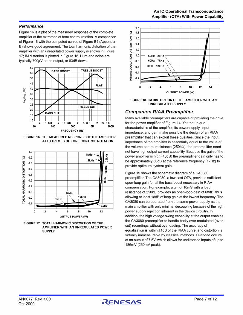
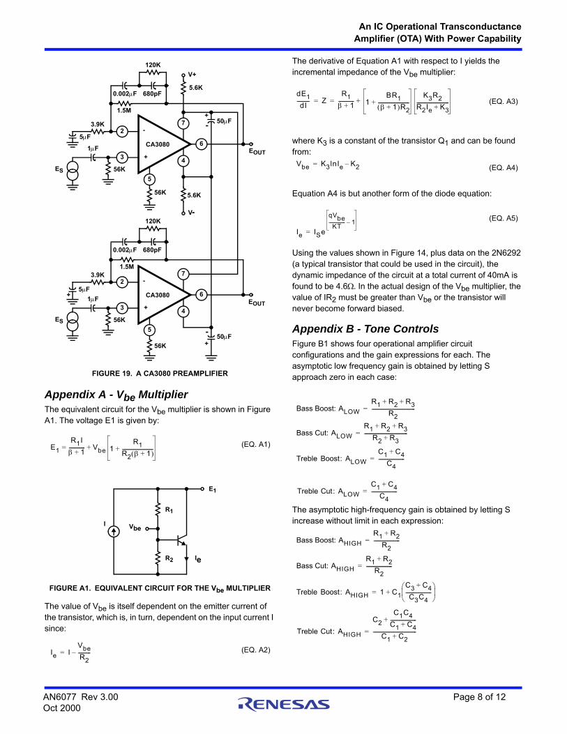
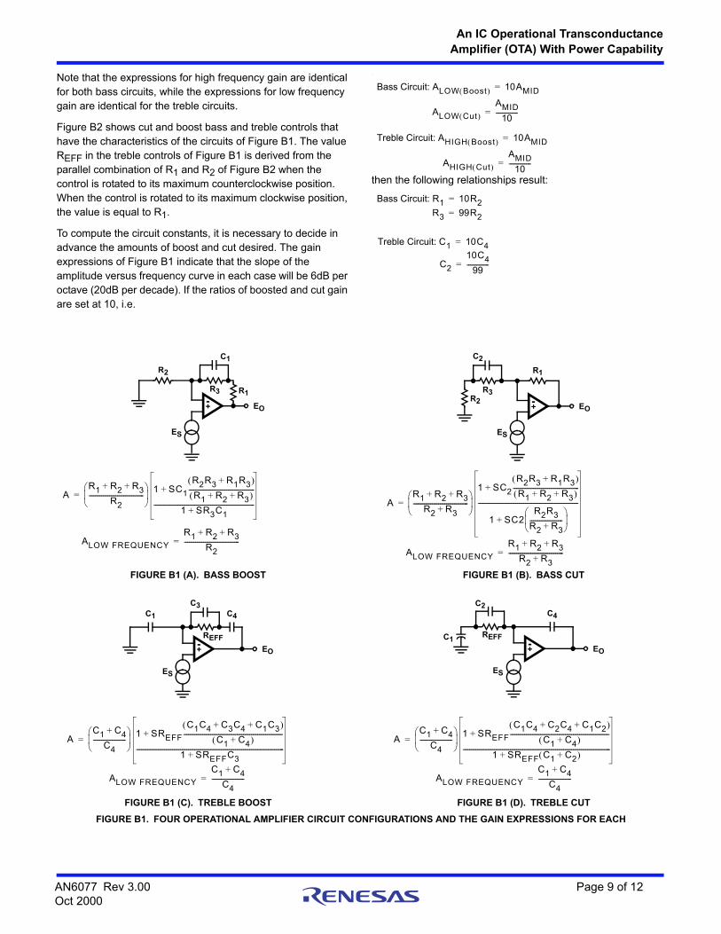
Performance
Figure 16 is a plot of the measured response of the complete amplifier at the extremes of tone control rotation. A comparison of Figure 16 with the computed curves of Figure B4 (Appendix B) shows good agreement. The total harmonic distortion of the amplifier with an unregulated power supply is shown in Figure 17; IM distortion is plotted in Figure 18. Hum and noise are typically 700V at the output, or 83dB down.
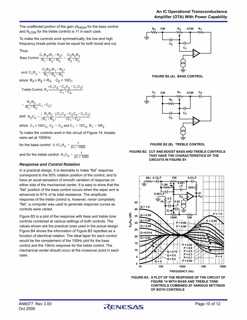
Companion RlAA PreamplifierMany available preamplifiers are capable of providing the drive for the power amplifier of Figure 14. Yet the unique characteristics of the amplifier, its power supply, input impedance, and gain make possible the design of an RIAA preamplifier that can exploit these qualities. Since the input impedance of the amplifier is essentially equal to the value of the volume control resistance (250k), the preamplifier need not have high output current capability. Because the gain of the power amplifier is high (40dB) the preamplifier gain only has to be approximately 30dB at the reference frequency (1kHz) to provide optimum system gain.
Figure 19 shows the schematic diagram of a CA3080 preamplifier. The CA3080, a low cost OTA, provides sufficient open-loop gain for all the bass boost necessary in RIAA compensation. For example, a gm of 10mS with a load resistance of 250k provides an open-loop gain of 68dB, thus allowing at least 18dB of loop gain at the lowest frequency. The CA3080 can be operated from the same power supply as the main amplifier with only minimal decoupling because of the high power supply rejection inherent in the device circuitry. In addition, the high voltage swing capability at the output enables the CA3080 preamplifier to handle badly over modulated (over-cut) recordings without overloading. The accuracy of equalization is within 1dB of the RIAA curve, and distortion is virtually immeasurable by classical methods. Overload occurs at an output of 7.5V, which allows for undistorted inputs of up to 186mV (260mV peak).
60
55
50
45
40
35
30
25
20
15
10
102 3 6 8
1002 3 68
10002 3 6 8
10K 100K2 3 6 8
BASS CUT
TREBLE CUT
FLAT
TREBLE BOOSTBASS BOOST
FREQUENCY (Hz)
EO
/ES
(d
B)
FIGURE 16. THE MEASURED RESPONSE OF THE AMPLIFIER AT EXTREMES OF TONE CONTROL ROTATION
1.0
0.1
0.2
0.3
0.4
0.5
0.6
0.7
0.8
0.9
2 4 6 8 10 12
OUTPUT POWER (W)
TO
TAL
HA
RM
ON
IC D
IST
OR
TIO
N (
%)
2kHz
4kHz
16kHz26kHz
1kHz
1kHz
26
kH
z1
6kH
z4
kHz
0
FIGURE 17. TOTAL HARMONIC DISTORTION OF THE AMPLIFIER WITH AN UNREGULATED POWER SUPPLY
2.0
1.8
1.6
1.4
1.2
1.0
0.8
0.6
0.4
0.2
0 2 4 6 8 10 12 14
OUTPUT POWER (W)
INT
ER
MO
DU
LA
TIO
N D
IST
OR
TIO
N (
%)
FIGURE 18. IM DISTORTION OF THE AMPLIFIER WITH AN UNREGULATED SUPPLY
60Hz 12kHz
60Hz 7kHz
60Hz 2kHz
AN6077 Rev 3.00 Page 7 of 12Oct 2000
An IC Operational Transconductance
Amplifier (OTA) With Power Capability
Appendix A - Vbe MultiplierThe equivalent circuit for the Vbe multiplier is shown in Figure A1. The voltage E1 is given by:
The value of Vbe is itself dependent on the emitter current of the transistor, which is, in turn, dependent on the input current I since:
The derivative of Equation A1 with respect to I yields the incremental impedance of the Vbe multiplier:
where K3 is a constant of the transistor Q1 and can be found from:
Equation A4 is but another form of the diode equation:
Using the values shown in Figure 14, plus data on the 2N6292 (a typical transistor that could be used in the circuit), the dynamic impedance of the circuit at a total current of 40mA is found to be 4.6. In the actual design of the Vbe multiplier, the value of IR2 must be greater than Vbe or the transistor will never become forward biased.
Appendix B - Tone ControlsFigure B1 shows four operational amplifier circuit configurations and the gain expressions for each. The asymptotic low frequency gain is obtained by letting S approach zero in each case:
The asymptotic high-frequency gain is obtained by letting S increase without limit in each expression:
3
CA3080
2
4
7
+
-3.9K
5.6K
V+
EOUT
6
56K
5
0.002F 680pF
1.5M
120K
50F
5F
1F
ES
56K 5.6K
3
CA3080
2
4
7
+
-3.9K
EOUT
6
56K
5
0.002F 680pF
1.5M
120K
5F
1F
ES
56K
-+
50F
-+
V-
FIGURE 19. A CA3080 PREAMPLIFIER
+
E1
R1I
1+-------------= Vbe 1
R1R2 1+ -------------------------++ (EQ. A1)
E1
IeR2
R1
VbeI
FIGURE A1. EQUIVALENT CIRCUIT FOR THE Vbe MULTIPLIER
Ie IVbeR2----------–= (EQ. A2)
dE1dI---------- Z
R1 1+------------- 1
BR1 1+ R2-------------------------+
K3R2R2Ie K3+--------------------------+= = (EQ. A3)
Vbe K3lnIe K2–= (EQ. A4)
Ie ISe
qVbeKT
--------------- 1–
=
(EQ. A5)
Bass Boost: ALOW
R1 R2 R3+ +
R2-----------------------------------=
Bass Cut: ALOW
R1 R2 R3+ +
R2 R3+-----------------------------------=
Treble Boost: ALOW
C1 C4+
C4---------------------=
Treble Cut: ALOW
C1 C4+
C4---------------------=
Bass Boost: AHIGH
R1 R2+
R2---------------------=
Bass Cut: AHIGH
R1 R2+
R2---------------------=
Treble Boost: AHIGH 1 C1
C3 C4+
C3C4---------------------
+=
Treble Cut: AHIGH
C2
C1C4C1 C4+---------------------+
C1 C2+-----------------------------------=
AN6077 Rev 3.00 Page 8 of 12Oct 2000
An IC Operational Transconductance
Amplifier (OTA) With Power Capability
Note that the expressions for high frequency gain are identical for both bass circuits, while the expressions for low frequency gain are identical for the treble circuits.
Figure B2 shows cut and boost bass and treble controls that have the characteristics of the circuits of Figure B1. The value REFF in the treble controls of Figure B1 is derived from the parallel combination of R1 and R2 of Figure B2 when the control is rotated to its maximum counterclockwise position. When the control is rotated to its maximum clockwise position, the value is equal to R1.
To compute the circuit constants, it is necessary to decide in advance the amounts of boost and cut desired. The gain expressions of Figure B1 indicate that the slope of the amplitude versus frequency curve in each case will be 6dB per octave (20dB per decade). If the ratios of boosted and cut gain are set at 10, i.e.
:
then the following relationships result:
Bass Circuit: ALOW Boost 10AMID=
ALOW Cut
AMID10
--------------=
Treble Circuit: AHIGH Boost 10AMID=
AHIGH Cut
AMID10
--------------=
Bass Circuit: R1 10R2=
R3 99R2=
Treble Circuit: C1 10C4=
C2
10C499
--------------=
FIGURE B1 (A). BASS BOOST FIGURE B1 (B). BASS CUT
FIGURE B1 (C). TREBLE BOOST FIGURE B1 (D). TREBLE CUT
FIGURE B1. FOUR OPERATIONAL AMPLIFIER CIRCUIT CONFIGURATIONS AND THE GAIN EXPRESSIONS FOR EACH
+-
R2
R1R3
C1
ES
EO
AR1 R2 R3+ +
R2----------------------------------- 1 SC1
R2R3 R1R3+
R1 R2 R3+ + ------------------------------------------+
1 SR3C1+----------------------------------------------------------------
=
ALOW FREQUENCY
R1 R2 R3+ +
R2-----------------------------------=
+-R2
R1
C2
ES
EO
R3
AR1 R2 R3+ +
R2 R3+-----------------------------------
1 SC2
R2R3 R1R3+
R1 R2 R3+ + ------------------------------------------+
1 SC2R2R3
R2 R3+---------------------
+
----------------------------------------------------------------=
ALOW FREQUENCY
R1 R2 R3+ +
R2 R3+-----------------------------------=
+-
REFF
C1
ES
EO
C4
C3
AC1 C4+
C4--------------------- 1 SREFF
C1C4 C3C4 C1C3+ +
C1 C4+ ---------------------------------------------------------------+
1 SREFFC3+----------------------------------------------------------------------------------------------
=
ALOW FREQUENCY
C1 C4+
C4---------------------=
+-
REFF
ES
EO
C4
C2
C1
AC1 C4+
C4--------------------- 1 SREFF
C1C4 C2C4 C1C2+ +
C1 C4+ ---------------------------------------------------------------+
1 SREFF C1 C2+ +----------------------------------------------------------------------------------------------
=
ALOW FREQUENCY
C1 C4+
C4---------------------=
AN6077 Rev 3.00 Page 9 of 12Oct 2000
An IC Operational Transconductance
Amplifier (OTA) With Power Capability
The unaffected portion of the gain (AHIGH for the bass control and ALOW for the treble control) is 11 in each case.
To make the controls work symmetrically, the low and high frequency break points must be equal for both boost and cut.
Thus:
since R3R2 + R3, C2 = 10C1
and
since
To make the controls work in the circuit of Figure 14, breaks were set at 1000Hz:
for the base control
and for the treble control
Response and Control Rotation
In a practical design, it is desirable to make “flat” response correspond to the 50% rotation position of the control, and to have an aural sensation of smooth variation of response on either side of the mechanical center. It is easy to show that the “flat” position of the bass control occurs when the wiper arm is advanced to 91% of its total resistance. The amplitude response of the treble control is, however, never completely “flat”; a computer was used to generate response curves as controls were varied.
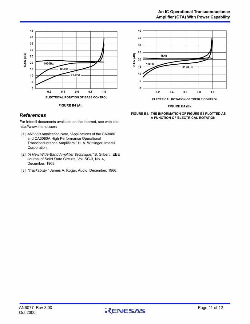
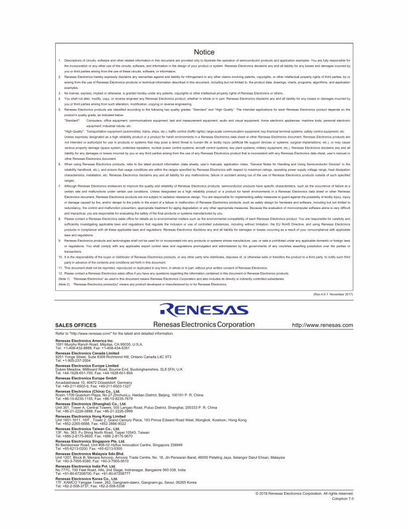
Figure B3 is a plot of the response with bass and treble tone controls combined at various settings of both controls. The values shown are the practical ones used in the actual design. Figure B4 shows the information of Figure B3 replotted as a function of electrical rotation. The ideal taper for each control would be the complement of the 100Hz plot for the bass control and the 10kHz response for the treble control. The mechanical center should occur at the crossover point in each case.
Bass Control:C1R3 R1 R2+
R1 R2 R3+ +------------------------------------------
C2R2R3R2 R3+-----------------------=
and C1R3
C2R3 R1 R2+
R1 R2 R3+ +------------------------------------------=
Treble Control: R1
C1C4 C3C4 C1C3+ +
C1 C4+---------------------------------------------------------------
R1R2R1 R2+--------------------- C1 C2+ =
R2C3
R1R2R1 R2+--------------------- C1C4 C2C4 C1C2+ +
C1 C4+ ---------------------------------------------------------------=
C1 100C2 C2, C3 and C1 10C4 R1, 9R2= = =
0.1C1R31
2 1000--------------------------=
R1C31
2 1000--------------------------=
R2 CW R3 CCW R1
C2C1
FIGURE B2 (A). BASS CONTROL
-+
C1 CW R1 CCW C4
C2
C3
R2
FIGURE B2 (B). TREBLE CONTROL
FIGURE B2. CUT AND BOOST BASS AND TREBLE CONTROLS THAT HAVE THE CHARACTERISTICS OF THE CIRCUITS IN FIGURE B1
-+
45
40
0
5
10
15
20
25
30
35
10 100 1000 10K 100K
FREQUENCY (Hz)
EO
/ES
(d
B)
68 15K 0.01F
0.0011.8K
0.12F
0.001F
820
EOES
0.020.2
1K
100K 10K
FF
Q = 1.0
Q = 0.99
Q = 0
Q = 0.98
Q = 0.96
Q =0.914
Q = 0.85
P = 1.0
P = 0.99
P = 0
P = 0.98P = 0.96
P = 0.92P = 0.8P = 0.5P = 0.3P = 0.1
P = 0.05
P
Q
F
FIGURE B3. A PLOT OF THE RESPONSE OF THE CIRCUIT OF FIGURE 14 WITH BASS AND TREBLE TONE CONTROLS COMBINED AT VARIOUS SETTINGS OF BOTH CONTROLS
-+
Q = 0.75Q = 0.5Q = 0.2
AN6077 Rev 3.00 Page 10 of 12Oct 2000
An IC Operational Transconductance
Amplifier (OTA) With Power Capability
ReferencesFor Intersil documents available on the internet, see web sitehttp://www.intersil.com/
[1] AN6668 Application Note, “Applications of the CA3080 and CA3080A High Performance Operational Transconductance Amplifiers,” H. A. Wittlinger, Intersil Corporation.
[2] “A New Wide-Band Amplifier Technique,” B. Gilbert, IEEE Journal of Solid State Circuits, Vol. SC-3, No. 4, December, 1968.
[3] “Trackability,” James A. Kogar, Audio, December, 1966.
45
0
5
10
15
20
25
30
35
40
0.2 0.4 0.6 0.8 1.0
ELECTRICAL ROTATION OF BASS CONTROL
GA
IN (
dB
)
1000Hz
100Hz
31.6Hz
FIGURE B4 (A).
1kHz
0
5
10
15
20
25
30
35
40
0.2 0.4 0.6 0.8 1.0
ELECTRICAL ROTATION OF TREBLE CONTROL
GA
IN (
dB
)
31.6kHz10kHz
FIGURE B4 (B).
FIGURE B4. THE INFORMATION OF FIGURE B3 PLOTTED AS A FUNCTION OF ELECTRICAL ROTATION
AN6077 Rev 3.00 Page 11 of 12Oct 2000
http://www.renesas.comRefer to "http://www.renesas.com/" for the latest and detailed information.
Renesas Electronics America Inc.1001 Murphy Ranch Road, Milpitas, CA 95035, U.S.A.Tel: +1-408-432-8888, Fax: +1-408-434-5351Renesas Electronics Canada Limited9251 Yonge Street, Suite 8309 Richmond Hill, Ontario Canada L4C 9T3Tel: +1-905-237-2004Renesas Electronics Europe LimitedDukes Meadow, Millboard Road, Bourne End, Buckinghamshire, SL8 5FH, U.KTel: +44-1628-651-700, Fax: +44-1628-651-804Renesas Electronics Europe GmbHArcadiastrasse 10, 40472 Düsseldorf, Germany Tel: +49-211-6503-0, Fax: +49-211-6503-1327Renesas Electronics (China) Co., Ltd.Room 1709 Quantum Plaza, No.27 ZhichunLu, Haidian District, Beijing, 100191 P. R. ChinaTel: +86-10-8235-1155, Fax: +86-10-8235-7679Renesas Electronics (Shanghai) Co., Ltd.Unit 301, Tower A, Central Towers, 555 Langao Road, Putuo District, Shanghai, 200333 P. R. China Tel: +86-21-2226-0888, Fax: +86-21-2226-0999Renesas Electronics Hong Kong LimitedUnit 1601-1611, 16/F., Tower 2, Grand Century Place, 193 Prince Edward Road West, Mongkok, Kowloon, Hong KongTel: +852-2265-6688, Fax: +852 2886-9022Renesas Electronics Taiwan Co., Ltd.13F, No. 363, Fu Shing North Road, Taipei 10543, TaiwanTel: +886-2-8175-9600, Fax: +886 2-8175-9670Renesas Electronics Singapore Pte. Ltd.80 Bendemeer Road, Unit #06-02 Hyflux Innovation Centre, Singapore 339949Tel: +65-6213-0200, Fax: +65-6213-0300Renesas Electronics Malaysia Sdn.Bhd.Unit 1207, Block B, Menara Amcorp, Amcorp Trade Centre, No. 18, Jln Persiaran Barat, 46050 Petaling Jaya, Selangor Darul Ehsan, MalaysiaTel: +60-3-7955-9390, Fax: +60-3-7955-9510Renesas Electronics India Pvt. Ltd.No.777C, 100 Feet Road, HAL 2nd Stage, Indiranagar, Bangalore 560 038, IndiaTel: +91-80-67208700, Fax: +91-80-67208777Renesas Electronics Korea Co., Ltd.17F, KAMCO Yangjae Tower, 262, Gangnam-daero, Gangnam-gu, Seoul, 06265 KoreaTel: +82-2-558-3737, Fax: +82-2-558-5338
SALES OFFICES
© 2018 Renesas Electronics Corporation. All rights reserved.Colophon 7.0
(Rev.4.0-1 November 2017)
Notice
1. Descriptions of circuits, software and other related information in this document are provided only to illustrate the operation of semiconductor products and application examples. You are fully responsible for
the incorporation or any other use of the circuits, software, and information in the design of your product or system. Renesas Electronics disclaims any and all liability for any losses and damages incurred by
you or third parties arising from the use of these circuits, software, or information.
2. Renesas Electronics hereby expressly disclaims any warranties against and liability for infringement or any other claims involving patents, copyrights, or other intellectual property rights of third parties, by or
arising from the use of Renesas Electronics products or technical information described in this document, including but not limited to, the product data, drawings, charts, programs, algorithms, and application
examples.
3. No license, express, implied or otherwise, is granted hereby under any patents, copyrights or other intellectual property rights of Renesas Electronics or others.
4. You shall not alter, modify, copy, or reverse engineer any Renesas Electronics product, whether in whole or in part. Renesas Electronics disclaims any and all liability for any losses or damages incurred by
you or third parties arising from such alteration, modification, copying or reverse engineering.
5. Renesas Electronics products are classified according to the following two quality grades: “Standard” and “High Quality”. The intended applications for each Renesas Electronics product depends on the
product’s quality grade, as indicated below.
"Standard": Computers; office equipment; communications equipment; test and measurement equipment; audio and visual equipment; home electronic appliances; machine tools; personal electronic
equipment; industrial robots; etc.
"High Quality": Transportation equipment (automobiles, trains, ships, etc.); traffic control (traffic lights); large-scale communication equipment; key financial terminal systems; safety control equipment; etc.
Unless expressly designated as a high reliability product or a product for harsh environments in a Renesas Electronics data sheet or other Renesas Electronics document, Renesas Electronics products are
not intended or authorized for use in products or systems that may pose a direct threat to human life or bodily injury (artificial life support devices or systems; surgical implantations; etc.), or may cause
serious property damage (space system; undersea repeaters; nuclear power control systems; aircraft control systems; key plant systems; military equipment; etc.). Renesas Electronics disclaims any and all
liability for any damages or losses incurred by you or any third parties arising from the use of any Renesas Electronics product that is inconsistent with any Renesas Electronics data sheet, user’s manual or
other Renesas Electronics document.
6. When using Renesas Electronics products, refer to the latest product information (data sheets, user’s manuals, application notes, “General Notes for Handling and Using Semiconductor Devices” in the
reliability handbook, etc.), and ensure that usage conditions are within the ranges specified by Renesas Electronics with respect to maximum ratings, operating power supply voltage range, heat dissipation
characteristics, installation, etc. Renesas Electronics disclaims any and all liability for any malfunctions, failure or accident arising out of the use of Renesas Electronics products outside of such specified
ranges.
7. Although Renesas Electronics endeavors to improve the quality and reliability of Renesas Electronics products, semiconductor products have specific characteristics, such as the occurrence of failure at a
certain rate and malfunctions under certain use conditions. Unless designated as a high reliability product or a product for harsh environments in a Renesas Electronics data sheet or other Renesas
Electronics document, Renesas Electronics products are not subject to radiation resistance design. You are responsible for implementing safety measures to guard against the possibility of bodily injury, injury
or damage caused by fire, and/or danger to the public in the event of a failure or malfunction of Renesas Electronics products, such as safety design for hardware and software, including but not limited to
redundancy, fire control and malfunction prevention, appropriate treatment for aging degradation or any other appropriate measures. Because the evaluation of microcomputer software alone is very difficult
and impractical, you are responsible for evaluating the safety of the final products or systems manufactured by you.
8. Please contact a Renesas Electronics sales office for details as to environmental matters such as the environmental compatibility of each Renesas Electronics product. You are responsible for carefully and
sufficiently investigating applicable laws and regulations that regulate the inclusion or use of controlled substances, including without limitation, the EU RoHS Directive, and using Renesas Electronics
products in compliance with all these applicable laws and regulations. Renesas Electronics disclaims any and all liability for damages or losses occurring as a result of your noncompliance with applicable
laws and regulations.
9. Renesas Electronics products and technologies shall not be used for or incorporated into any products or systems whose manufacture, use, or sale is prohibited under any applicable domestic or foreign laws
or regulations. You shall comply with any applicable export control laws and regulations promulgated and administered by the governments of any countries asserting jurisdiction over the parties or
transactions.
10. It is the responsibility of the buyer or distributor of Renesas Electronics products, or any other party who distributes, disposes of, or otherwise sells or transfers the product to a third party, to notify such third
party in advance of the contents and conditions set forth in this document.
11. This document shall not be reprinted, reproduced or duplicated in any form, in whole or in part, without prior written consent of Renesas Electronics.
12. Please contact a Renesas Electronics sales office if you have any questions regarding the information contained in this document or Renesas Electronics products.
(Note 1) “Renesas Electronics” as used in this document means Renesas Electronics Corporation and also includes its directly or indirectly controlled subsidiaries.
(Note 2) “Renesas Electronics product(s)” means any product developed or manufactured by or for Renesas Electronics.


![Non-linear circuits with CCII+/- current conveyors(Balanced Operational Transconductance Amplifier) amplifiers by Maxim [3], and the LM13600 amplifiers by National Semiconductor [4]](https://img.pdfslide.net/doc/110x75/60b7f09eea4c942c766bad73/non-linear-circuits-with-ccii-current-conveyors-balanced-operational-transconductance.jpg)
![A Built in Self Test System for Dynamic Performance ... · the test stimulus an oscillator circuit can be used [7]. The Operational Transconductance Amplifier and Capacitor (OTA-C)](https://img.pdfslide.net/doc/110x75/5fc768800c90ea5d227f0137/a-built-in-self-test-system-for-dynamic-performance-the-test-stimulus-an-oscillator.jpg)


![Operational Transconductance Amplifier (OTA) in 45nm CMOS · Amplifier (OTA) in 45nm CMOS YOUNGSEOK LEE ... Design of Analog CMOS Integrated Circuits. McGraw-Hill, 2002. [2] B. Ahuja,](https://img.pdfslide.net/doc/110x75/5fbfc7035b7a87264a188ff5/operational-transconductance-amplifier-ota-in-45nm-cmos-amplifier-ota-in-45nm.jpg)