Embed Size (px)
Citation preview
Xilinx/ Synopsys Interface Guide
Xilinx/Synopsys Interface Guide— ISE 4 Printed in U.S.A.
Xilinx/Synopsys Interface Guide
The Xilinx logo shown above is a registered trademark of Xilinx, Inc.
CoolRunner, RocketChips, RocketIP, Spartan, StateBENCH, StateCAD, Virtex, XACT, XILINX, XC2064,XC3090, XC4005, and XC5210 are registered trademarks of Xilinx, Inc.
The shadow X shown above is a trademark of Xilinx, Inc.
ACE Controller, ACE Flash, A.K.A. Speed, Alliance Series, AllianceCORE, Bencher, ChipScope, ConfigurableLogic Cell, CORE Generator, CoreLINX, Dual Block, EZTag, Fast CLK, Fast CONNECT, Fast FLASH, FastMap,Fast Zero Power, Foundation, Gigabit Speeds...and Beyond!, HardWire, HDL Bencher, IRL, J Drive, JBits, LCA,LogiBLOX, Logic Cell, LogiCORE, LogicProfessor, MicroBlaze, MicroVia, MultiLINX, NanoBlaze, PicoBlaze,PLUSASM, PowerGuide, PowerMaze, QPro, Real-PCI, Rocket I/O, Select I/O, SelectRAM, SelectRAM+, SiliconXpresso, Smartguide, Smart-IP, SmartSearch, SMARTswitch, System ACE, Testbench In A Minute, TrueMap,UIM, VectorMaze, VersaBlock, VersaRing, Wave Table, WebFITTER, WebPACK, WebPOWERED, XABEL,XACTstep Advanced, XACTstep Foundry, XACT-Floorplanner, XACT-Performance, XAM, XAPP, X-BLOX +,XChecker, XDM, XEPLD, Xilinx Foundation Series, Xilinx XDTV, Xinfo, XSI, XtremeDSP, all XC designatedproducts, and ZERO+ are trademarks of Xilinx, Inc. The Programmable Logic Company is a service mark of Xilinx,Inc.
All other trademarks are the property of their respective owners.
Xilinx, Inc. does not assume any liability arising out of the application or use of any product described or shownherein; nor does it convey any license under its patents, copyrights, or maskwork rights or any rights of others.Xilinx, Inc. reserves the right to make changes, at any time, in order to improve reliability, function or design andto supply the best product possible. Xilinx, Inc. will not assume responsibility for the use of any circuitry describedherein other than circuitry entirely embodied in its products. Xilinx, Inc. devices and products are protected underone or more of the following U.S. Patents: 4,642,487; 4,695,740; 4,706,216; 4,713,557; 4,746,822; 4,750,155;4,758,985; 4,820,937; 4,821,233; 4,835,418; 4,855,619; 4,855,669; 4,902,910; 4,940,909; 4,967,107; 5,012,135;5,023,606; 5,028,821; 5,047,710; 5,068,603; 5,140,193; 5,148,390; 5,155,432; 5,166,858; 5,224,056; 5,243,238;5,245,277; 5,267,187; 5,291,079; 5,295,090; 5,302,866; 5,319,252; 5,319,254; 5,321,704; 5,329,174; 5,329,181;5,331,220; 5,331,226; 5,332,929; 5,337,255; 5,343,406; 5,349,248; 5,349,249; 5,349,250; 5,349,691; 5,355,035;5,357,153; 5,360,747; 5,361,229; 5,362,999; 5,365,125; 5,367,207; 5,386,154; 5,394,104; 5,397,943; 5,399,924;5,399,925; 5,406,133; 5,410,189; 5,410,194; 5,414,377; 5,422,833; 5,426,378; 5,426,379; 5,430,687; 5,432,719;5,448,181; 5,448,493; 5,450,021; 5,450,022; 5,453,706; 5,455,525; 5,466,117; 5,469,003; 5,475,253; 5,477,414;5,481,206; 5,483,478; 5,486,707; 5,486,776; 5,488,316; 5,489,858; 5,489,866; 5,491,353; 5,495,196; 5,497,108;5,498,979; 5,498,989; 5,499,192; 5,500,608; 5,500,609; 5,502,000; 5,502,440; 5,504,439; 5,504,440; 5,506,518;5,506,523; 5,506,878; 5,513,124; 5,517,135; 5,521,835; 5,521,837; 5,523,963; 5,523,971; 5,524,097; 5,526,322;5,528,169; 5,528,176; 5,530,378; 5,530,384; 5,546,018; 5,550,839; 5,550,843; 5,552,722; 5,553,001; 5,559,751;5,561,367; 5,561,629; 5,561,631; 5,563,527; 5,563,528; 5,563,529; 5,563,827; 5,565,792; 5,566,123; 5,570,051;5,570,059; 5,574,634; 5,574,655; 5,578,946; 5,581,198; 5,581,199; 5,581,738; 5,583,450; 5,583,452; 5,592,105;5,594,367; 5,598,424; 5,600,263; 5,600,264; 5,600,271; 5,600,597; 5,608,342; 5,610,536; 5,610,790; 5,610,829;5,612,633; 5,614,844; 5,617,021; 5,617,041; 5,617,327; 5,617,573; 5,623,387; 5,627,480; 5,629,637; 5,629,886;5,631,577; 5,631,583; 5,635,851; 5,636,368; 5,640,106; 5,642,058; 5,646,545; 5,646,547; 5,646,564; 5,646,903;5,648,732; 5,648,913; 5,650,672; 5,650,946; 5,652,904; 5,654,631; 5,654,665; 5,656,950; 5,657,290; 5,659,484;5,661,660; 5,661,685; 5,668,495; 5,670,896; 5,670,897; 5,672,966; 5,673,198; 5,675,262; 5,675,270; 5,675,589;5,677,638; 5,682,107; 5,684,413; 5,689,133; 5,689,516; 5,691,907; 5,691,912; 5,694,047; 5,694,055; 5,694,056;5,694,399; 5,696,454; 5,701,091; 5,701,441; 5,703,759; 5,705,932; 5,705,938; 5,708,597; 5,712,579; 5,714,890;5,715,197; 5,717,340; 5,719,506; 5,719,507; 5,724,276; 5,726,484; 5,726,584; 5,734,866; 5,734,868; 5,737,234;5,737,235; 5,737,631; 5,742,178; 5,742,179; 5,742,531; 5,744,974; 5,744,979; 5,744,981; 5,744,995; 5,748,942;
R
ii Xilinx Development System
5,748,979; 5,752,006; 5,752,035; 5,754,459; 5,758,192; 5,760,603; 5,760,604; 5,760,607; 5,761,483; 5,764,076;5,764,534; 5,764,564; 5,768,179; 5,770,951; 5,773,993; 5,778,439; 5,781,756; 5,784,313; 5,784,577; 5,786,240;5,787,007; 5,789,938; 5,790,479; 5,790,882; 5,795,068; 5,796,269; 5,798,656; 5,801,546; 5,801,547; 5,801,548;5,808,479; 5,811,985; 5,815,004; 5,815,016; 5,815,404; 5,815,405; 5,818,255; 5,818,730; 5,821,772; 5,821,774;5,825,202; 5,825,662; 5,825,787; 5,828,230; 5,828,231; 5,828,236; 5,828,608; 5,831,448; 5,831,460; 5,831,845;5,831,907; 5,835,402; 5,838,167; 5,838,901; 5,838,954; 5,841,296; 5,841,867; 5,844,422; 5,844,424; 5,844,829;5,844,844; 5,847,577; 5,847,579; 5,847,580; 5,847,993; 5,852,323; 5,861,761; 5,862,082; 5,867,396; 5,870,309;5,870,327; 5,870,586; 5,874,834; 5,875,111; 5,877,632; 5,877,979; 5,880,492; 5,880,598; 5,880,620; 5,883,525;5,883,852; 5,886,538; 5,889,411; 5,889,412; 5,889,413; 5,889,701; 5,892,681; 5,892,961; 5,894,420; 5,896,047;5,896,329; 5,898,319; 5,898,320; 5,898,602; 5,898,618; 5,898,893; 5,907,245; 5,907,248; 5,909,125; 5,909,453;5,910,732; 5,912,937; 5,914,514; 5,914,616; 5,920,201; 5,920,202; 5,920,223; 5,923,185; 5,923,602; 5,923,614;5,928,338; 5,931,962; 5,933,023; 5,933,025; 5,933,369; 5,936,415; 5,936,424; 5,939,930; 5,940,606; 5,942,913;5,944,813; 5,945,837; 5,946,478; 5,949,690; 5,949,712; 5,949,983; 5,949,987; 5,952,839; 5,952,846; 5,955,888;5,956,748; 5,958,026; 5,959,821; 5,959,881; 5,959,885; 5,961,576; 5,962,881; 5,963,048; 5,963,050; 5,969,539;5,969,543; 5,970,142; 5,970,372; 5,971,595; 5,973,506; 5,978,260; 5,986,958; 5,990,704; 5,991,523; 5,991,788;5,991,880; 5,991,908; 5,995,419; 5,995,744; 5,995,988; 5,999,014; 5,999,025; 6,002,268; 6,002,282; 6,002,991;6,005,423; 6,005,829; 6,008,666; 6,011,407; 6,011,740; 6,016,063; 6,018,250; 6,018,624; 6,020,633; 6,020,756;6,020,757; 6,020,776; 6,021,423; 6,023,564; 6,023,565; 6,025,736; 6,026,481; 6,028,445; 6,028,450; 6,033,938;6,034,542; 6,034,548; 6,034,557; 6,035,106; 6,037,800; 6,038,386; 6,041,340; 6,043,692; 6,044,012; 6,044,025;6,046,603; 6,047,115; 6,049,222; 6,049,227; 6,051,992; 6,054,871; 6,055,205; 6,057,589; 6,057,704; 6,057,708;6,061,417; 6,061,418; 6,067,508; 6,069,488; 6,069,489; 6,069,490; 6,069,849; 6,070,260; 6,071,314; 6,072,348;6,073,154; 6,074,432; 6,075,418; 6,078,201; 6,078,209; 6,078,528; 6,078,735; 6,078,736; 6,081,914; 6,084,429;6,086,629; 6,086,631; 6,091,262; 6,091,263; 6,091,892; 6,094,063; 6,094,065; 6,094,385; 6,097,210; 6,097,238;6,099,583; 6,100,705; 6,101,132; 6,101,143; 6,104,211; 6,105,105; 6,107,821; 6,107,826; 6,107,827; 6,112,322;6,114,843; 6,118,286; 6,118,298; 6,118,300; 6,118,324; 6,118,869; 6,118,938; 6,120,549; 6,120,551; 6,121,795;6,124,724; 6,124,731; 6,130,550; 6,133,751; 6,134,191; 6,134,517; 6,137,307; 6,137,714; 6,144,220; 6,144,225;6,144,262; 6,144,933; 6,150,838; 6,150,839; 6,150,863; 6,154,048; 6,154,049; 6,154,052; 6,154,053; 6,157,209;6,157,211; 6,157,213; 6,160,418; 6,160,431; 6,163,167; 6,167,001; 6,167,416; 6,167,545; 6,167,558; 6,167,560;6,172,518; 6,172,519; 6,172,520; 6,173,241; 6,175,246; 6,175,530; 6,177,819; 6,177,830; 6,181,158; 6,181,164;6,184,708; 6,184,709; 6,184,712; 6,185,724; 6,188,091; 6,191,610; 6,191,613; 6,191,614; 6,192,436; 6,195,774;6,199,192; 6,201,406; 6,201,410; 6,201,411; and 6,202,106; Re. 34,363, Re. 34,444, and Re. 34,808. Other U.S.and foreign patents pending. Xilinx, Inc. does not represent that devices shown or products described herein arefree from patent infringement or from any other third party right. Xilinx, Inc. assumes no obligation to correct anyerrors contained herein or to advise any user of this text of any correction if such be made. Xilinx, Inc. will notassume any liability for the accuracy or correctness of any engineering or software support or assistance providedto a user.
Xilinx products are not intended for use in life support appliances, devices, or systems. Use of a Xilinx product insuch applications without the written consent of the appropriate Xilinx officer is prohibited.
Copyright 1991-2001 Xilinx, Inc. All Rights Reserved.
Xilinx/Synopsys Interface Guide iii

Xilinx/Synopsys Interface Guide
iv Xilinx Development System
About This Manual
This manual describes the Xilinx/Synopsys Interface (XSI) program, a tool used for implementing Field Programmable Gate Array (FPGA) designs using either Synopsys FPGA Compiler, FPGA Compiler II, or the Design Compiler synthesis tools.
This manual does not cover the use of Synopsys FPGA Express with the XSI program.
Before using this manual, you should be familiar with the operations that are common to all Xilinx software tools: how to bring up the system, select a tool for use, specify operations, and manage design data. These topics are covered in the Development System Reference Guide. Other publications you can consult for related information are the LogiBLOX Guide, and Libraries Guide.
Manual ContentsThis book contains the following chapters.
• “Introduction to the Xilinx/Synopsys Interface” chapter“Introduction to the Xilinx/Synopsys Interface” chapter provides information on the XSI Design Flow, FPGA compiler, FPGA compiler II, and Design Compiler. This chapter also includes a list of additional documentation.
• “Getting Started” chapter“Getting Started” chapter shows how to verify your software installation, modify your Synopsys startup file, and run Synlibs to set the link and target libraries.
• “Synthesizing Your Design with FPGA Compiler II” chapter“Synthesizing your Design with FPGA Compiler II”
Xilinx/Synopsys Interface Guide v
Xilinx/Synopsys Interface Guide
chapter shows how to port code from FPGA Compiler to FPGA Compiler II, convert script files from FPGA Compiler and Design Compiler and includes design information on attribute passing, IOB configuration, clock buffers, memory, boundary scan, the Global Set/Reset net, and timing specifications.
• The “Synthesizing Your Design with FPGA Compiler and Design Compiler” chapter“Synthesizing Your Design with FPGA Compiler and Design Compiler” chapter includes design information on wire-load models, IOB configuration, clock buffers, memory, boundary scan, the Global Set/Reset net, timing specifications, compiling, area reports, debugging, implementing, and saving your designs.
• The “Using CORE Generator and LogiBLOX” chapter“Using Core Generator and LogiBLOX” chapter provides information about using Core Generator and LogiBLOX to create high-level modules for your design.
• “Simulating Your Design” chapter“Simulating Your Design” chapter describes how to perform RTL and timing simulation.
• “Using Files, Programs, and Libraries” chapter“Using Files, Programs, and Libraries” chapter describes the files, programs, and Xilinx-supplied libraries you need to translate your HDL design using FPGA Compiler or Design Compiler.
• The “XSI Library Primitives” appendix“lists the primitives you can synthesize or instantiate in a VHDL or Verilog HDL file.
• The “Targeting Virtex Devices” appendix“describes how to apply the XSI design flow to Virtex devices.
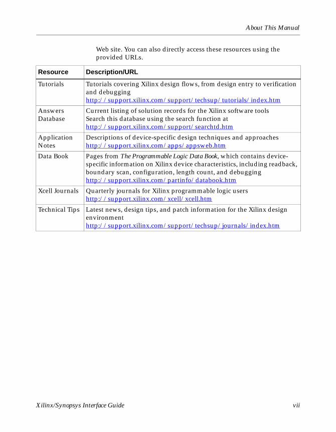
Additional ResourcesFor additional information, go to http://support.xilinx.com. The following table lists some of the resources you can access from this
vi Xilinx Development System
About This Manual
Web site. You can also directly access these resources using the provided URLs.
Resource Description/URL
Tutorials Tutorials covering Xilinx design flows, from design entry to verification and debugginghttp://support.xilinx.com/support/techsup/tutorials/index.htm
Answers Database
Current listing of solution records for the Xilinx software toolsSearch this database using the search function athttp://support.xilinx.com/support/searchtd.htm
Application Notes
Descriptions of device-specific design techniques and approacheshttp://support.xilinx.com/apps/appsweb.htm
Data Book Pages from The Programmable Logic Data Book, which contains device-specific information on Xilinx device characteristics, including readback, boundary scan, configuration, length count, and debugginghttp://support.xilinx.com/partinfo/databook.htm
Xcell Journals Quarterly journals for Xilinx programmable logic usershttp://support.xilinx.com/xcell/xcell.htm
Technical Tips Latest news, design tips, and patch information for the Xilinx design environmenthttp://support.xilinx.com/support/techsup/journals/index.htm
Xilinx/Synopsys Interface Guide vii

Xilinx/Synopsys Interface Guide
viii Xilinx Development System
Conventions
This manual uses the following conventions. An example illustrates most conventions.
TypographicalThe following conventions are used for all documents.
• Courier font indicates messages, prompts, and program files that the system displays.
speed grade: - 100
• Courier bold indicates literal commands that you enter in a syntactical statement. However, braces “{ }” in Courier bold are not literal and square brackets “[ ]” in Courier bold are literal only in the case of bus specifications, such as bus [7:0].
rpt_del_net=
Courier bold also indicates commands that you select from a menu.
File → Open
• Italic font denotes the following items.
♦ Variables in a syntax statement for which you must supply values
edif2ngd design_name
♦ References to other manuals
See the Development System Reference Guide for more information.
Xilinx/Synopsys Interface Guide vii
Xilinx/Synopsys Interface Guide
♦ Emphasis in text
If a wire is drawn so that it overlaps the pin of a symbol, the two nets are not connected.
• Square brackets “[ ]” indicate an optional entry or parameter. However, in bus specifications, such as bus [7:0], they are required.
edif2ngd [option_name] design_name
• Braces “{ }” enclose a list of items from which you must choose one or more.
lowpwr ={on|off}
• A vertical bar “|” separates items in a list of choices.
lowpwr ={on|off}
• A vertical ellipsis indicates repetitive material that has been omitted.
IOB #1: Name = QOUT’
IOB #2: Name = CLKIN’
.
.
.
• A horizontal ellipsis “…” indicates that an item can be repeated one or more times.
allow block block_name loc1 loc2 … locn;
Online DocumentThe following conventions are used for online documents.
• Blue text indicates cross-references within a book. Red text indicates cross-references to other books. Click the colored text to jump to the specified cross-reference.
• Blue, underlined text indicates a Web site. Click the link to open the specified Web site. You must have a Web browser and internet connection to use this feature.
viii Xilinx Development System
Contents
About This ManualManual Contents ...........................................................................vAdditional Resources ....................................................................v
ConventionsTypographical ................................................................................viiOnline Document ..........................................................................viii
Chapter 1 Introduction to the Xilinx/Synopsys Interface
What Is XSI? .................................................................................1-1XSI Design Flow Using FPGA Compiler II ....................................1-2XSI Design Flow Using FPGA Compiler .......................................1-3Comparing Design Compiler to FPGA Compiler and FPGA Compiler II 1-6Using FPGA Compiler II ................................................................1-7Xilinx Documentation Set ..............................................................1-7
Chapter 2 Getting Started
Setting Up the Synopsys Interface ................................................2-1Setting up the XDW and Simulation Libraries ...............................2-2
Compiling XDW Libraries .........................................................2-3Modifying the Default Synopsys Startup File ................................2-5
Checking the FPGA Compiler Setup File .................................2-6Checking the Design Compiler Setup File ...............................2-7
Examples of Synopsys Setup Files ...............................................2-9XC4000 Devices ......................................................................2-9
Example .synopsys_dc.setup File ......................................2-9Example .synopsys_dc.setup File ......................................2-12Example Script File for Virtex Devices ................................2-14
Verifying Software Installation .......................................................2-20
Chapter 3 Synthesizing Your Design with FPGA Compiler II
Before You Begin ..........................................................................3-2Naming Conventions .....................................................................3-2Porting Code from FPGA Compiler to FPGA Compiler II ..............3-2Converting Script Files from FPGA Compiler and Design Compiler 3-3Synthesizing the Design ................................................................3-4Entering Design Constraints and Controls ....................................3-8Specifying Timing Constraints .......................................................3-10
Specifying Clock Constraints ...................................................3-11Specifying Path Group Constraints .....................................3-13Specifying I/O Constraints ..................................................3-14Timing Subpaths .................................................................3-15Defining Multicycle Timing Constraints ...............................3-16Adding Pull-Up and Pull-Down Resistors ...........................3-20
Optimizing a Design Implementation ............................................3-21Optimizing Logic Across Hierarchical Boundaries ...................3-21
Xilinx/Synopsys Interface Guide 1
Xilinx/Synopsys Interface Guide
Using a Flattening Optimization Strategy ...........................3-23Setting Port Attributes and Constraints ....................................3-23
Evaluating Timing Delays ..............................................................3-24Using the FPGA Compiler II Time Tracker ..............................3-25Viewing the Results of Optimization ........................................3-26Generating Reports for Debugging ..........................................3-29Viewing the Schematics ...........................................................3-30
Exporting the Netlist ......................................................................3-30Using the Xilinx Development System ..........................................3-31HDL Coding Techniques ...............................................................3-31
Configuring IOBs ......................................................................3-31All Architectures .......................................................................3-32
Optimizing Inputs ................................................................3-32Understanding and Using Slew Rate ..................................3-32
Using IOBs ...............................................................................3-32Using Input Blocks ..............................................................3-32Using Output Blocks ...........................................................3-33Using Bidirectional Mode ....................................................3-34
Inserting Bidirectional I/Os ............................................................3-35Assigning Pad Locations ..........................................................3-35Instantiating a Registered Bidirectional I/O ..............................3-35
Implementing 3-State Registered Output ......................................3-37Example of Not Directly Driving the 3-State Signal ..................3-37Example of Directly Driving the 3-State Signal ........................3-39
Attribute Passing ...........................................................................3-41Implementing Clock Buffers ..........................................................3-43Using Memory ...............................................................................3-44
Implementing Virtex/E/2 RAM ..................................................3-45Implementing XC4000 RAM ....................................................3-45
Performing Boundary Scan ...........................................................3-48Using the Global Set/Reset Net ....................................................3-53
Implementing GSR Buffers ......................................................3-54Accessing Global Set/Reset Using STARTBUF ......................3-57Synthesizing/Simulating for VHDL Global Set/Reset Emulation 3-57
Instantiating a STARTUP Block in VHDL ...........................3-58Increasing Performance with the GSR Net ..............................3-59
Chapter 4 Synthesizing Your Design with FPGA Compiler and De-sign Compiler
Before You Begin ..........................................................................4-2Naming Conventions .....................................................................4-2Setting the Wire-Load Model .........................................................4-3Setting the Operating Condition Parameters ................................4-3Configuring IOBs ...........................................................................4-3
All Architectures .......................................................................4-4Optimizing Inputs ................................................................4-4Understanding and Using Slew Rate ..................................4-4
XC3000A/L and XC3100A/L IOBs ...........................................4-5Using Input Blocks ..............................................................4-5
2 Xilinx Development System
Contents
Using Output Blocks ...........................................................4-6Using Bidirectional Mode ....................................................4-6Using Input Blocks ..............................................................4-7Using Output Blocks ...........................................................4-7Using Bidirectional Mode ....................................................4-8
Using XC5200 IOBs .................................................................4-9Using Input Blocks ..............................................................4-9Using Output Blocks ...........................................................4-9
Assigning Pad Locations ..........................................................4-10Example of Not Directly Driving the 3-State Signal ............4-11Example of Directly Driving the 3-State Signal ...................4-13
Inserting Bidirectional I/Os .......................................................4-14Instantiating a Registered Bidirectional I/O .........................4-15Compiling Bidirectional I/O .................................................4-17
Using Unbonded IOBs .............................................................4-22Adding Pull-Up and Pull-Down Resistors .................................4-22Removing the Default Input Delay ...........................................4-23Initializing the IOB Flip-Flop to Preset ......................................4-23
Inserting Clock Buffers ..................................................................4-23Controlling Clock Buffer Insertion ............................................4-24Determining the Number of Clock Buffers ...............................4-26Preventing the Insertion of Clock Buffers .................................4-27
Using Memory ...............................................................................4-27Implementing XC4000 RAMs ...................................................4-28Implementing RAM In Virtex Devices ......................................4-31
Performing Boundary Scan ...........................................................4-32Using the Global Set/Reset Net ....................................................4-37
Accessing Global Set/Reset Using STARTBUF ......................4-38Synthesizing/Simulating for VHDL Global Set/Reset Emulation 4-39
Using STARTBUF in VHDL ................................................4-39Instantiating a STARTUP Block in VHDL ...........................4-40
Setting Direct Preset or Direct Clear ........................................4-40Increasing Performance with the GSR Net ..............................4-40
Using the Xilinx DesignWare Library .............................................4-44Improving Design Area and Speed ..........................................4-44
Creating Timing Specifications ......................................................4-45Following the DC2NCF Design Flow .......................................4-47
Creating the Netlist and Script File (Design Compiler) .......4-47Creating the Netlist and Script File (FPGA Compiler) .........4-48
Understanding DC2NCF Translation Limitations .....................4-49Limitations of Create Clock .................................................4-50Limitations of Set Input Delay and Set Output Delay ..........4-50Limitations of Set Max Delay and Set False Path ...............4-52Set Multicycle Path .............................................................4-55
Compiling Your Design .................................................................4-56Optimizing Logic Across Hierarchical Boundaries ...................4-56
Using a Flattening Optimization Strategy ...........................4-58Compiling the Design with Hierarchy ..................................4-58Compiling the Design without Hierarchy .............................4-59
Compiling a Design with Instantiated I/O Cells ........................4-59
Xilinx/Synopsys Interface Guide 3
Xilinx/Synopsys Interface Guide
Compiling XC4000, Spartan, and Virtex Designs ....................4-60Creating the Area Report ..............................................................4-64Evaluating Timing Delays ..............................................................4-65Generating Reports for Debugging ...............................................4-66
Generating a Configuration Report ..........................................4-67Generating a Hierarchical Schematic ......................................4-70Creating a Level for Each CLB and IOB ..................................4-70Generating a Level for Each Function Generator ....................4-71
Writing and Saving Your Design ...................................................4-71Saving the DB File ...................................................................4-71Replacing CLBs and IOBs with Gates .....................................4-72
Invoking the Replace FPGA Command ..............................4-72Replacing CLBs and IOBs in Designs with Hierarchy ........4-72
Controlling the Synopsys Mapping ..........................................4-73Restoring BLKNM Attributes ...............................................4-74
Setting the Design Part Type ...................................................4-74Saving the Design Netlist File ..................................................4-74
Saving your Netlist in EDIF Format (Design Compiler) ......4-74Saving your Netlist in XNF Format (FPGA Compiler) .........4-75
Using the Xilinx Development System ..........................................4-76
Chapter 5 Using CORE Generator and LogiBLOX
Using CORE Generator ................................................................5-1Specifying Inputs and Outputs in LogiBLOX .................................5-2Using LogiBLOX in the HDL Design Flow .....................................5-3Instantiating RAM ..........................................................................5-4
Instantiating RAM or ROM with FPGA Compiler .....................5-15Instantiating RAM or ROM with FPGA Compiler II ..................5-18
Simulation Design Flow Overview .................................................6-2Using Simulation Libraries ............................................................6-3
UniSim Library .........................................................................6-3UniSim Library Structure .....................................................6-4UniSim Library Files ............................................................6-5UniSim Library Component Instantiation ............................6-6
SimPrim Library .......................................................................6-6LogiBLOX Library .....................................................................6-6
LogiBLOX Library Compilation ...........................................6-6LogiBLOX Library Component Instantiation .......................6-7
Working with the VITAL Standard .................................................6-7VHDL and Verilog Simulation Flow ...............................................6-7
Simulating at Register Transfer Level (RTL) ............................6-8Conducting a Post-Synthesis (pre-NGDBuild) Gate-Level Functional Simulation ................................................................................6-9Conducting a Post-NGDBuild (Pre-Map) Gate-Level Functional Simu-lation ........................................................................................6-9Conducting a Post-Route Full Timing (Block and Net Delays) Simula-tion ...........................................................................................6-10
Synthesizing/Simulating for VHDL Global Set/Reset Emulation ...6-10Instantiating a STARTUP Block in VHDL .................................6-11
4 Xilinx Development System
Contents
Using ROCBUF in VHDL .........................................................6-13Generating a 3-State-On-Configuration in VHDL .....................6-13Using TOCBUF in VHDL ..........................................................6-14Using Oscillators in VHDL ........................................................6-14Using Global Set/Reset Emulation in Verilog ...........................6-15Using Global 3-State Emulation in Verilog ...............................6-15Using Oscillators in Verilog ......................................................6-15
NGDBuild Support of Multiple Device Architectures .....................6-15Recommended VSS Simulation Strategy .....................................6-16VSS Simulation Flow .....................................................................6-17Editing the VSS Setup File ............................................................6-18Creating a Testbench File .............................................................6-20Using RTL Simulation ...................................................................6-20Implementing Your Design ............................................................6-22Understanding the XSI Directory Structure ...................................7-1Using File Descriptions .................................................................7-4Using Program Descriptions .........................................................7-6Using Supplied Libraries Descriptions ..........................................7-7
Finding Supported Part Types and Speed Grades ..................7-12Finding Unsupported Part Types and Speed Grades ..............7-12
Appendix A XSI Library PrimitivesGenerating a List of XSI Library Primitives ...................................A-2Obtaining XSI Library Primitive Pin Order .....................................A-3Alphabetical List of Primitives for All Architectures .......................A-3
Using the Dont Touch Attribute ................................................A-4Setting the INIT Attribute ..........................................................A-4Primitive Name Suffixes ...........................................................A-4Virtex-Specific Primitive Name Suffixes ...................................A-5Architecture Abbreviations .......................................................A-6Primitive Tables .......................................................................A-7
Understanding Virtex-Specific Cell Names ...................................A-33Virtex-Specific Primitives Table ...............................................A-34Virtex RAM Primitive Name Suffixes ........................................A-37
Xilinx DesignWare Modules ..........................................................A-40Post-Configuration Initialization States .........................................A-42
Appendix B Targeting Virtex DevicesFollowing General Guidelines .......................................................B-1Setting FPGA Compiler to Synthesize a Virtex Design .................B-2Synthesizing a Virtex Design into FPGA Compiler .......................B-4Setting VSS Simulation for Virtex ..................................................B-5Setting FPGA Compiler II for Virtex ..............................................B-5Synthesizing a Virtex Design in FPGA Compiler II .......................B-6Using Clock Delay Locked Loops with Synopsys .........................B-6
Xilinx/Synopsys Interface Guide 5

Xilinx/Synopsys Interface Guide
6 Xilinx Development System
Chapter 1
Introduction to the Xilinx/Synopsys Interface
This chapter describes the Xilinx/Synopsys Interface (XSI), compares FPGA Compiler, FPGA Compiler II, and Design Compiler, and lists additional Xilinx and Synopsys documentation you can use in conjunction with this manual. This chapter includes the following sections.
• “What Is XSI?”
• “XSI Design Flow Using FPGA Compiler II”
• “XSI Design Flow Using FPGA Compiler”
• “Comparing Design Compiler to FPGA Compiler and FPGA Compiler II”
• “Using FPGA Compiler II”
• “Xilinx Documentation Set”
What Is XSI?XSI supports Synopsys FPGA Compiler Version 1999.05 or later, FPGA Compiler II Version 3.3 or later, and Synopsys Design Compiler Version 1999.05 or later.
This manual does not cover the use of Synopsys FPGA Express.
Use the XSI design tool kit to implement Xilinx Field Programmable Gate Array (FPGA) designs using either Synopsys FPGA Compiler, FPGA Compiler II, or Design Compiler. These Synopsys High-Level Design Automation (HLDA) tools allow you to create and optimize circuit designs from hardware descriptions written in VHSIC Hardware Description Language (VHDL) or Verilog HDL. Library support for XC4000E/L/EX/XL/XLA/XV, XC5200, XC9000,
Xilinx/Synopsys Interface Guide 1-1
Xilinx/Synopsys Interface Guide
Spartan/XL/-II, and Virtex/E/-II devices includes a Xilinx DesignWare (XDW) library.
Before you start creating your FPGA designs, refer to the most current version of the ISE 4 Release Notes and Installation Guide for information about the following topics.
• XSI installation instructions
• Tutorial on the tools
• Reference information on common instantiated components
• Constraints guide
For the latest information on Xilinx parts and software, visit the Xilinx Web site at http://www.xilinx.com.
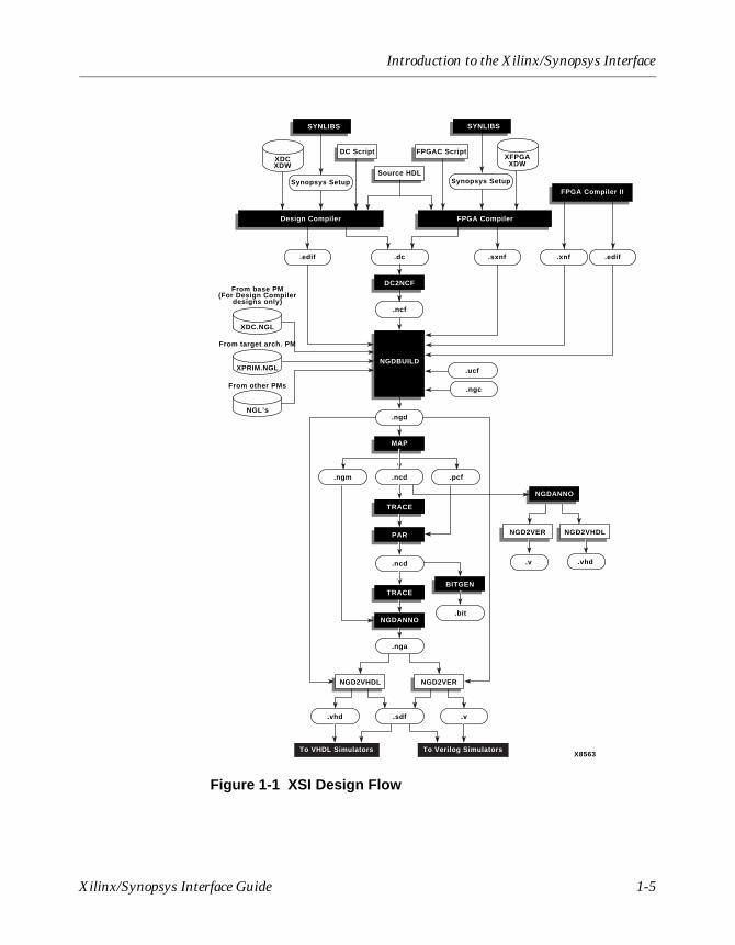
XSI Design Flow Using FPGA Compiler IIFigure 1-1 illustrates the following required steps you follow to implement and simulate your HDL designs using FPGA Compiler II.
Refer to the XSI Synopsys tutorials at http://support.xilinx.com/support/techsup/tutorials/index.htm for step-by-step instructions on converting your HDL designs.
1. Synthesize your design with FPGA Compiler II.
2. Save your design as an EDIF file.
3. Run NGDBuild on the EDIF file to create an NGD file.
4. Run the MAP program on the NGD file to create a mapped NCD file.
5. Run the TRACE program to determine if PAR meets your timing goals.
6. Run PAR on the NCD file to place and route your design.
7. Run TRACE again on your placed and routed design.
8. Run NGDAnno on your routed NCD and NGM files to create an NGA file.
9. Run either NGD2VHDL or NGD2VER on the NGA file to create a VHDL (VHD) or Verilog (V) file for simulation with the appropriate simulators for back annotation. These two programs
1-2 Xilinx Development System
Introduction to the Xilinx/Synopsys Interface
also create a Standard Delay Format (SDF) file containing timing information.
10. Run the BitGen program to create a bitstream for programming the FPGA.
XSI Design Flow Using FPGA CompilerFigure 1-1 illustrates the following required steps you follow to implement and simulate your HDL designs using FPGA Compiler.
Refer to the XSI Synopsys tutorials at http://support.xilinx.com/support/techsup/tutorials/index.htm for step-by-step instructions on converting your HDL designs.
1. Use the Synlibs program to determine the appropriate libraries for your design.
2. Synthesize your design with either FPGA Compiler or Design Compiler.
3. Save your design as an SXNF file or an SEDIF file, along with a DC file that contains Synopsys constraints. Make sure you use the .sxnf or .sedif file extension as NGDBuild will recognize that the netlists are coming from FPGA Compiler or Design Compiler.
4. Use the DC2NCF program to translate the Synopsys constraints DC file to a Netlist Constraints File (NCF).
5. Run NGDBuild on the SXNF or SEDIF file to create an NGD file.
6. Run the MAP program on the NGD file to create a mapped NCD file.
7. Run the TRACE program to determine if PAR meets your timing goals.
8. Run PAR on the NCD file to place and route your design.
9. Run TRACE again on your placed and routed design.
10. Run NGDAnno on your routed NCD and NGM files to create an NGA file.
11. Run either NGD2VHDL or NGD2VER on the NGA file to create a VHDL (VHD) or Verilog (V) file for simulation with the appropriate simulators for back annotation. These two programs
Xilinx/Synopsys Interface Guide 1-3
Xilinx/Synopsys Interface Guide
also create a Standard Delay Format (SDF) file containing timing information.
12. Run the BitGen program to create a bitstream for programming the FPGA.
1-4 Xilinx Development System
Introduction to the Xilinx/Synopsys Interface
Figure 1-1 XSI Design Flow
XPRIM.NGL
NGL’s
Source HDL
NGD2VHDL NGD2VER
DC2NCF
SYNLIBS SYNLIBS
NGDBUILD
Design Compiler FPGA Compiler
FPGA Compiler II
.dc
.ncf
.ngc
.ngd
.ngm .ncd
.ncd
.pcf
.edif .sxnf
.sdf.vhd .v
XDCXDW
NGD2VER NGD2VHDL
Synopsys Setup Synopsys Setup
DC Script FPGAC Script
.edif.xnf
XFPGAXDW
MAP
PAR
.nga
NGDANNO
NGDANNO
To VHDL Simulators To Verilog Simulators
XDC.NGL
From base PM(For Design Compiler
designs only)
From target arch. PM
From other PMs
X8563
.ucf
TRACE
TRACEBITGEN
.bit
.vhd.v
Xilinx/Synopsys Interface Guide 1-5
Xilinx/Synopsys Interface Guide
Comparing Design Compiler to FPGA Compiler and FPGA Compiler II
XSI contains libraries for the following device families:
• XC4000™/E/EX/L/XL/XLA/XV
• XC9000™
• Spartan™/XL/-II
• CoolRunner™ XPLA3
• Virtex™/-E/-II
You can use either FPGA Compiler, FPGA Compiler II, or Design Compiler to synthesize a design for these devices. Generally, for XC4000L and XC4000XL devices, you can use the XC4000E and the XC4000EX synthesis libraries, respectively.
This manual assumes that you use FPGA Compiler or FPGA Compiler II synthesis tools for XC4000, XC5200, XC9000, Spartan, and Virtex devices. If you do not have FPGA Compiler or FPGA Compiler II, XSI provides XC4000, XC5200, XC9000, Spartan, and Virtex libraries to use with Design Compiler. You can use FPGA Compiler or FPGA Compiler II for XC3000 and XC3100 devices, but the libraries for these devices use the Design Compiler synthesis features.
Design Compiler offers the following features.
• Optimizes flip-flops without clock enables, and latches in the input/output block (IOB)
• Optimizes 3-state buffers in the IOB
• Encodes one-hot state machines
• Automatically uses the configurable logic block (CLB) Clock Enable pin
FPGA Compiler and FPGA Compiler II offers the previously described Design Compiler features, as well as the following.
• Optimizes logic to the XC4000 and Spartan/XL CLB and IOB architectures
• Reports area and timing by device architecture, for example, CLB, IOB, and 3-state buffer
1-6 Xilinx Development System
Introduction to the Xilinx/Synopsys Interface
• Passes timing constraints to the core tools
• Uses lookup table (LUT) optimization for XC3000A/L, XC3100A/L, XC5200, Spartan-II, and Virtex devices. These new libraries that use the LUT optimization allow FPGA Compiler and FPGA Compiler II to synthesize your design to a collection of lookup tables, registers, and I/O pads.
Using FPGA Compiler IIFPGA Compiler II, a logic-synthesis and optimization tool, allows you to create optimized netlists from VHDL, Verilog, and existing unoptimized FPGA netlists. FPGA Compiler II (Version 3.2 or better) offers the following features.
• Provides an integrated text editor for entering VHDL and Verilog source code for your design
• Analyzes HDL source files for correct syntax, accepting any combination of VHDL, Verilog, and FPGA netlist files as sources
• Synthesizes logic from VHDL, Verilog, and FPGA netlist sources
• Optimizes logic for speed and area according to design constraints
• Contains integrated schematic viewing and static timing analysis
• Extracts and displays accurate post-synthesis delay information
Synopsys provides FPGA Compiler II libraries used for Xilinx products.
Xilinx Documentation SetThe following documents provide additional design information.
• Development System Reference Guide provides detailed information on the programs found in Xilinx software.
• LogiBLOX Guide describes the LogiBLOX program, a tool used to create high-level modules for insertion into your HDL design.
• Libraries Guide presents information about the various Xilinx-provided primitives and macros.
• ISE 4.x Release Notes Documentation describes installation setup and current issues regarding the use of the Synopsys interface.
Xilinx/Synopsys Interface Guide 1-7
Xilinx/Synopsys Interface Guide
• For converting an XACT 5.xx Synopsys design to M1, refer to the Xilinx Software Conversion Guide from XACTstep v.5.X.X to XACTstep vM1.X.X.
1-8 Xilinx Development System
Chapter 2
Getting Started
This chapter provides information on setting up the Xilinx Synopsys Interface (XSI) and associated libraries. Example files are included to help you set up the FPGA Compiler with the Xilinx software. This chapter also describes how to verify your software installation, modify the .synopsys_dc.setup file, and use the Synlibs program to determine the correct XSI libraries for FPGA Compiler or Design Compiler. You will also find general information about using the interface.
Read this chapter before you begin either the FPGA Compiler or Design Compiler tutorials located at http://www.support.xilinx.com/support/techsup/tutorials/index.htm.
This chapter includes the following sections.
• “Setting Up the Synopsys Interface”
• “Setting up the XDW and Simulation Libraries”
• “Modifying the Default Synopsys Startup File”
• “Examples of Synopsys Setup Files”
• “Verifying Software Installation”
Setting Up the Synopsys InterfaceThe following environment variables must be modified or added to run the Synopsys interface tools.
• SYNOPSYS (add)
• PATH (modify)
• LD_LIBRARY_PATH (modify)
• SHLIB_PATH (modify)
Xilinx/Synopsys Interface Guide 2-1
Xilinx/Synopsys Interface Guide
Set these variables as follows.
setenv SYNOPSYS installation_path_to_synopsysset path = ($XILINX/bin/platform_name \$SYNOPSYS/platform_name/syn/bin \$SYNOPSYS/platform_name/sim/bin \$path)
For Solaris only.
setenv LD_LIBRARY_PATH $SYNOPSYS/platform_name/sim/lib:$LD_LIBRARY_PATH
For HP/UX only.
setenv SHLIB_PATH $SYNOPSYS/platform_name/sim/lib:$SHLIB_PATH
The following is an example.
setenv SYNOPSYS /usr/synopsysset path = ($XILINX/bin/sol \$SYNOPSYS/sol/syn/bin \$SYNOPSYS/sol/sim/bin \$path)setenv LD_LIBRARY_PATH $SYNOPSYS/sol/sim/
lib:$LD_LIBRARY_PATH
Setting up the XDW and Simulation LibrariesNote If you are not using FPGA Compiler II v3.3 or a later, you must re-compile the Xilinx DesignWare (XDW) libraries.
The XSI (Xilinx Synopsys Interface) simulation and XDW (Xilinx DesignWare) libraries are compiled for Synopsys v1999.05. If you are using the latest version of XSI with a version of Synopsys newer than v1999.05, you must re-compile the XDW libraries with the version of Synopsys you are using. If you are going to simulate with VSS, you must re-compile the simulation libraries.
Compiling the libraries in the $XILINX area requires write permissions to this area. If you copy the $XILINX/synopsys directory to a local area, you do not need rewrite permissions for the $XILINX area to re-compile the libraries. However, verify that the .synopsys_dc.setup and .synopsys_vss.setup files use the local copy.
2-2 Xilinx Development System
Getting Started
Compiling XDW LibrariesFollow these steps to compile the XDW libraries.
1. Set up your Xilinx and Synopsys software environments.
2. Go to the $XILINX/synopsys/libraries/dw/src directory.
3. In this directory, there are subdirectories that represent the Xilinx device families that have XDW libraries. If you are going to use any of the device families listed, you must go to the corresponding subdirectory and run the .dc compile script in that directory. For example, for a Spartan device, enter the following commands.
cd spartan
Run the install_dw.dc script by entering the following.
dc_shell -f install_dw.dc
4. When the script is finished, go back to $XILINX/synopsys/libraries/dw/src. Repeat these steps for each device you plan on using.
Xilinx/Synopsys Interface Guide 2-3
Xilinx/Synopsys Interface Guide
Compiling the Simulation LibrariesNote The following procedure is for compiling the XSI simulation libraries with VSS. If you are using a different HDL simulator, refer to your simulator’s documentation for instructions on compiling HDL simulation libraries.
1. Setup your XSI and Synopsys software environments.
2. Go to the $XILINX/synopsys/libraries/sim/src directory.
3. In this directory, there are subdirectories that represent the five simulation libraries, described as follows.
♦ LogiBLOX — for functional simulation of VHDL designs with instantiated LogiBLOX components
♦ SimPrims — timing simulation library
♦ UNISIMS — functional simulation library
♦ XC9000 — XC9500 functional simulation library
♦ XDW — Functional simulation library for post-synthesis (FPGA compiler) pre-NGDBuild simulation
Some or all of these libraries need to be re-compiled depending on the device and type of simulation you plan on using. Xilinx recommends compiling the logiblox, simprims, and unisims libraries. Use the following steps to compile these libraries.
4. Go to the logiblox directory and enter the following command.
./analyze.csh
Go back to the $XILINX/synopsys/libraries/sim/src directory.
5. Go to the simprims directory and enter the following command.
./analyze.csh
Go back to the $XILINX/synopsys/libraries/sim/src directory.
6. Go to the unisims directory and enter the following command.
./analyze.csh
2-4 Xilinx Development System
Getting Started
The unisims directory also contains the analyze_52k.csh script. If you plan on simulating XC5200 devices, you must run this script as well. You must also edit the .synopsys_dc.setup file in the unisims directory to point to a location for the compiled XC5200 libraries.
Go back to the $XILINX/synopsys/libraries/sim/src directory.
7. Go to the xdw directory and enter the following command.
./analyze.csh
Go back to the $XILINX/synopsys/libraries/sim/src directory.
8. Go to the xc9000/ftgs directory and enter the following command.
dc_shell -f install_xc9000.dc
Modifying the Default Synopsys Startup FileThe startup file for the Synopsys synthesis tools is .synopsys_dc.setup. This file contains the search path for the XSI libraries, Synopsys libraries, and user libraries. XSI provides a template Synopsys startup file.
XSI provides the template.synopsys_dc.setup_dc and template.synopsys_dc.setup_fc template files. You can find the template files in the $XILINX/synopsys/examples directory. Use template.synopsys_dc.setup_dc if you use Design Compiler; use template.synopsys_dc.setup_fc if you use FPGA Compiler.
$SYNOPSYS is the directory where the Synopsys software resides. If you do not know the location of this directory, enter the following at the system prompt.
echo $SYNOPSYS
If you already have a .synopsys_dc.setup file, you must modify your file to include the commands found in the Xilinx-supplied template startup files.
If you do not already have a Synopsys startup file, copy the appropriate Xilinx-supplied startup file to your home or working directory and rename it as follows.
Xilinx/Synopsys Interface Guide 2-5
Xilinx/Synopsys Interface Guide
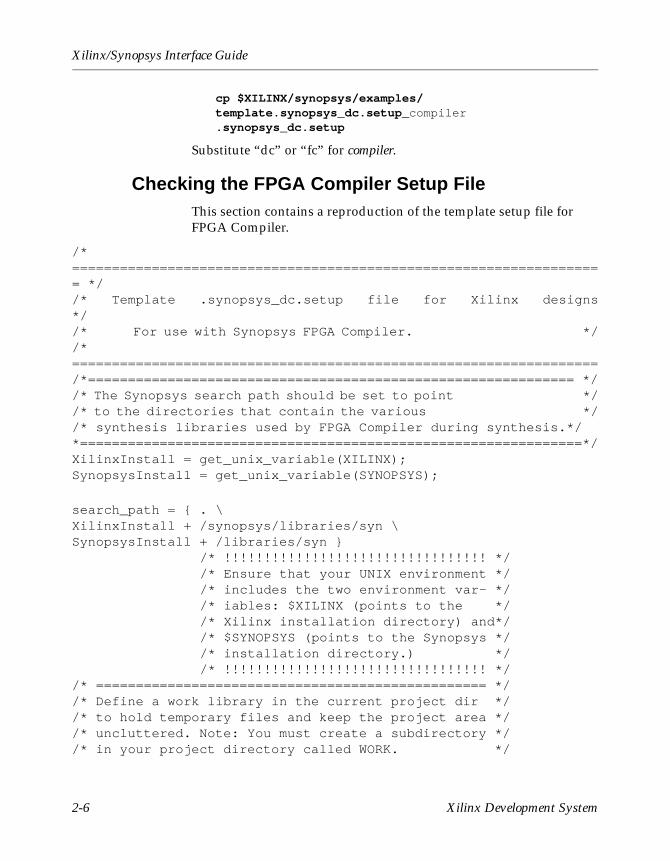
cp $XILINX/synopsys/examples/ template.synopsys_dc.setup_compiler .synopsys_dc.setup
Substitute “dc” or “fc” for compiler.
Checking the FPGA Compiler Setup FileThis section contains a reproduction of the template setup file for FPGA Compiler.
/*=================================================================== *//* Template .synopsys_dc.setup file for Xilinx designs*//* For use with Synopsys FPGA Compiler. *//*==================================================================/*============================================================= *//* The Synopsys search path should be set to point *//* to the directories that contain the various *//* synthesis libraries used by FPGA Compiler during synthesis.*/*===============================================================*/XilinxInstall = get_unix_variable(XILINX);SynopsysInstall = get_unix_variable(SYNOPSYS);
search_path = { . \XilinxInstall + /synopsys/libraries/syn \SynopsysInstall + /libraries/syn }
/* !!!!!!!!!!!!!!!!!!!!!!!!!!!!!!!!! *//* Ensure that your UNIX environment *//* includes the two environment var- *//* iables: $XILINX (points to the *//* Xilinx installation directory) and*//* $SYNOPSYS (points to the Synopsys *//* installation directory.) *//* !!!!!!!!!!!!!!!!!!!!!!!!!!!!!!!!! */
/* ================================================= *//* Define a work library in the current project dir *//* to hold temporary files and keep the project area *//* uncluttered. Note: You must create a subdirectory */ /* in your project directory called WORK. */
2-6 Xilinx Development System
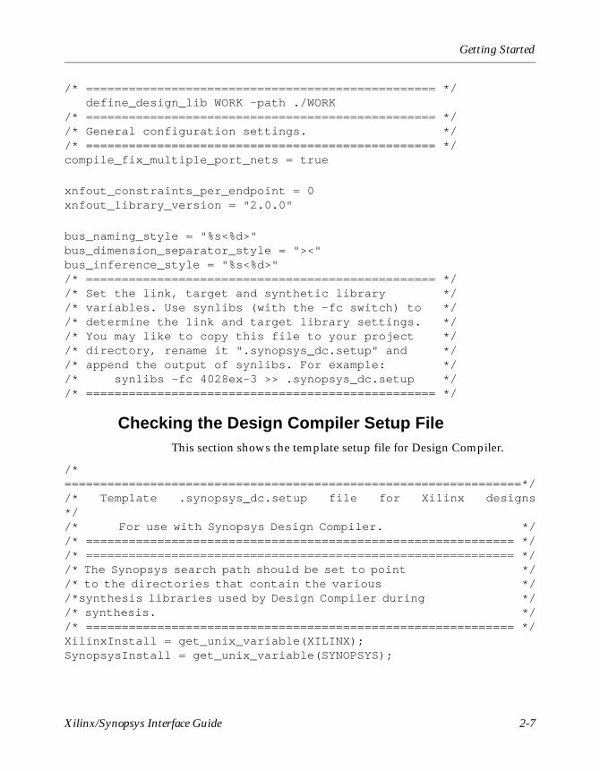
Getting Started
/* ================================================= */ define_design_lib WORK -path ./WORK/* ================================================= *//* General configuration settings. *//* ================================================= */compile_fix_multiple_port_nets = true
xnfout_constraints_per_endpoint = 0xnfout_library_version = "2.0.0"
bus_naming_style = "%s<%d>"bus_dimension_separator_style = "><"bus_inference_style = "%s<%d>"/* ================================================= *//* Set the link, target and synthetic library *//* variables. Use synlibs (with the -fc switch) to *//* determine the link and target library settings. *//* You may like to copy this file to your project *//* directory, rename it ".synopsys_dc.setup" and *//* append the output of synlibs. For example: *//* synlibs -fc 4028ex-3 >> .synopsys_dc.setup *//* ================================================= */
Checking the Design Compiler Setup FileThis section shows the template setup file for Design Compiler.
/* ================================================================*//* Template .synopsys_dc.setup file for Xilinx designs*//* For use with Synopsys Design Compiler. *//* ============================================================ *//* ============================================================ *//* The Synopsys search path should be set to point *//* to the directories that contain the various *//*synthesis libraries used by Design Compiler during *//* synthesis. *//* ============================================================ */XilinxInstall = get_unix_variable(XILINX);SynopsysInstall = get_unix_variable(SYNOPSYS);
Xilinx/Synopsys Interface Guide 2-7
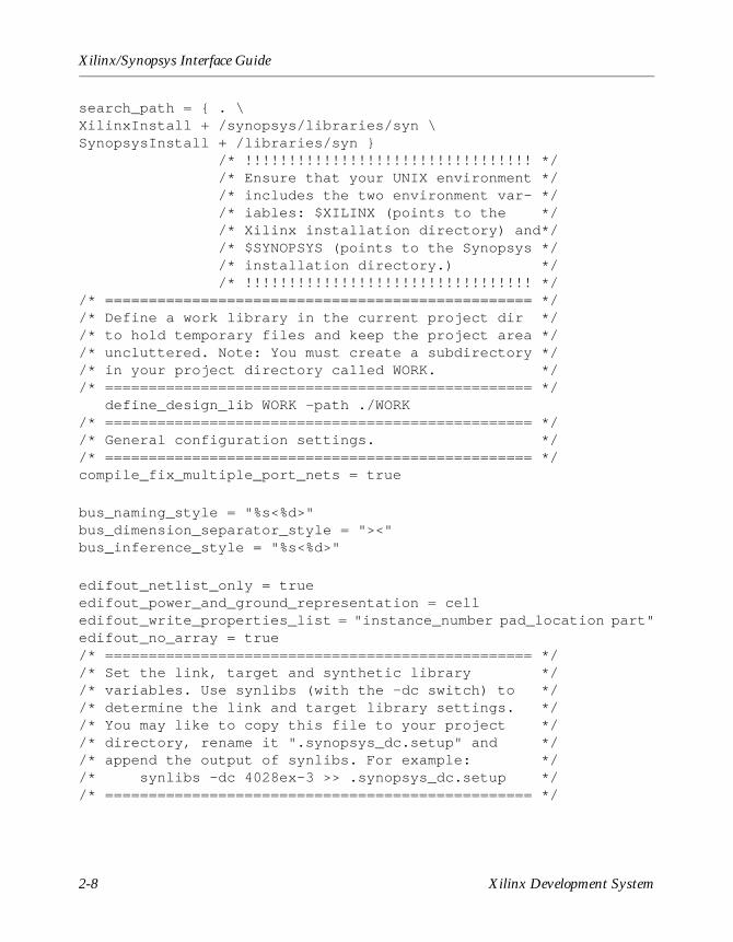
Xilinx/Synopsys Interface Guide
search_path = { . \XilinxInstall + /synopsys/libraries/syn \SynopsysInstall + /libraries/syn } /* !!!!!!!!!!!!!!!!!!!!!!!!!!!!!!!!! */ /* Ensure that your UNIX environment */ /* includes the two environment var- */ /* iables: $XILINX (points to the */ /* Xilinx installation directory) and*/ /* $SYNOPSYS (points to the Synopsys */ /* installation directory.) */ /* !!!!!!!!!!!!!!!!!!!!!!!!!!!!!!!!! *//* ================================================= *//* Define a work library in the current project dir *//* to hold temporary files and keep the project area *//* uncluttered. Note: You must create a subdirectory */ /* in your project directory called WORK. *//* ================================================= */ define_design_lib WORK -path ./WORK/* ================================================= *//* General configuration settings. *//* ================================================= */compile_fix_multiple_port_nets = true
bus_naming_style = "%s<%d>"bus_dimension_separator_style = "><"bus_inference_style = "%s<%d>"
edifout_netlist_only = trueedifout_power_and_ground_representation = celledifout_write_properties_list = "instance_number pad_location part"edifout_no_array = true/* ================================================= *//* Set the link, target and synthetic library *//* variables. Use synlibs (with the -dc switch) to *//* determine the link and target library settings. *//* You may like to copy this file to your project *//* directory, rename it ".synopsys_dc.setup" and *//* append the output of synlibs. For example: *//* synlibs -dc 4028ex-3 >> .synopsys_dc.setup *//* ================================================= */
2-8 Xilinx Development System
Getting Started
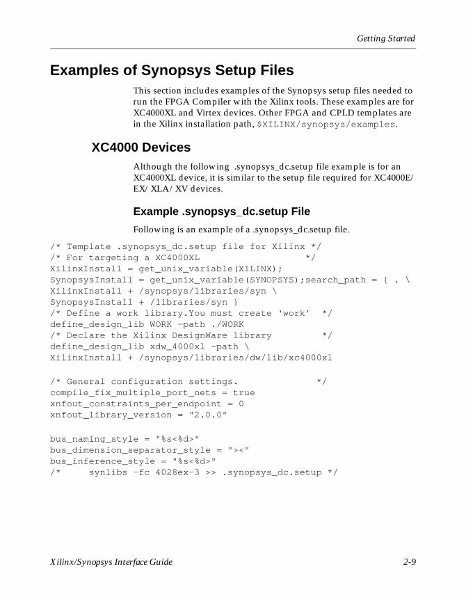
Examples of Synopsys Setup FilesThis section includes examples of the Synopsys setup files needed to run the FPGA Compiler with the Xilinx tools. These examples are for XC4000XL and Virtex devices. Other FPGA and CPLD templates are in the Xilinx installation path, $XILINX/synopsys/examples.
XC4000 DevicesAlthough the following .synopsys_dc.setup file example is for an XC4000XL device, it is similar to the setup file required for XC4000E/EX/XLA/XV devices.
Example .synopsys_dc.setup File
Following is an example of a .synopsys_dc.setup file.
/* Template .synopsys_dc.setup file for Xilinx *//* For targeting a XC4000XL */XilinxInstall = get_unix_variable(XILINX);SynopsysInstall = get_unix_variable(SYNOPSYS);search_path = { . \XilinxInstall + /synopsys/libraries/syn \SynopsysInstall + /libraries/syn }/* Define a work library.You must create ‘work’ */define_design_lib WORK -path ./WORK/* Declare the Xilinx DesignWare library */define_design_lib xdw_4000xl -path \XilinxInstall + /synopsys/libraries/dw/lib/xc4000xl
/* General configuration settings. */compile_fix_multiple_port_nets = truexnfout_constraints_per_endpoint = 0xnfout_library_version = "2.0.0"
bus_naming_style = "%s<%d>"bus_dimension_separator_style = "><"bus_inference_style = "%s<%d>"/* synlibs -fc 4028ex-3 >> .synopsys_dc.setup */
Xilinx/Synopsys Interface Guide 2-9
Xilinx/Synopsys Interface Guide
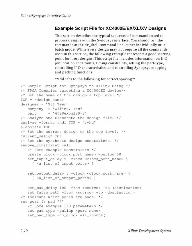
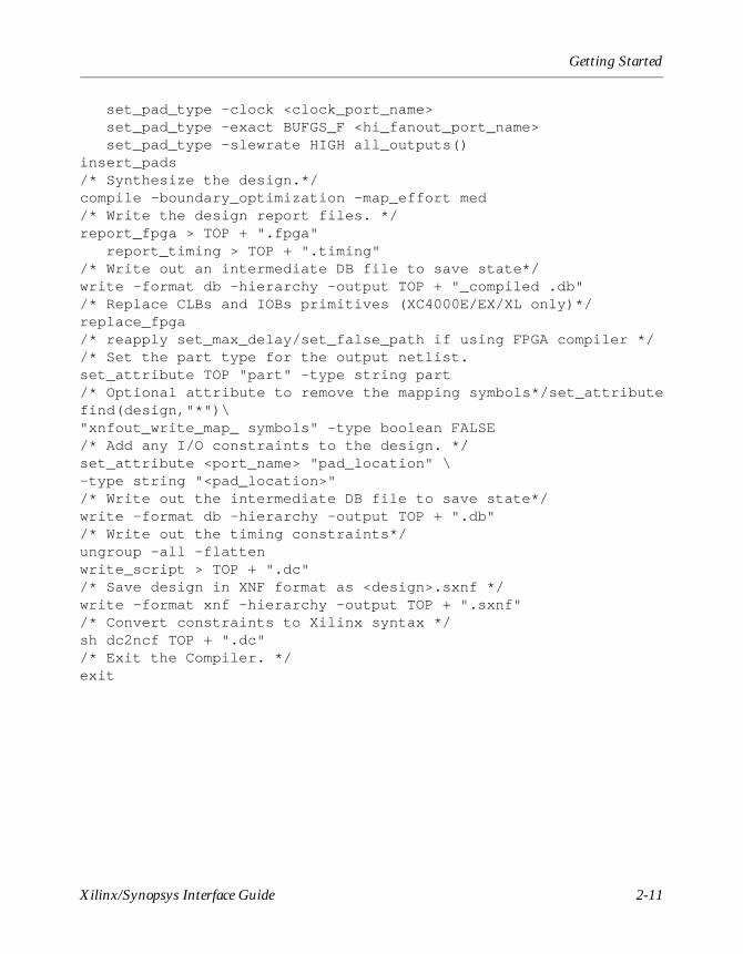
Example Script File for XC4000E/EX/XL/XV Designs
This section describes the typical sequence of commands used to process designs with the Synopsys interface. You should run the commands at the dc_shell command line, either individually or in batch mode. While every design may not require all the commands used in this section, the following example represents a good starting point for most designs. This script file includes information on I/O pin location constraints, timing constraints, setting the part-type, controlling I/O characteristics, and controlling Synopsys mapping and packing functions.
**add tabs to the following for correct spacing**
/* Sample Script for Synopsys to Xilinx Using *//* FPGA Compiler targeting a XC4000EX device*//* Set the name of the design’s top-level */TOP = <design_name>designer = "XSI Team" company = "Xilinx, Inc" part = "4028expg299-3"/* Analyze and Elaborate the design file. */analyze -format vhdl TOP + ".vhd"elaborate TOP/* Set the current design to the top level. */current_design TOP/* Set the synthesis design constraints. */remove_constraint -all /* Some example constraints */ create_clock <clock_port_name> -period 50 set_input_delay 5 -clock <clock_port_name> \ { <a_list_of_input_ports> }
set_output_delay 5 -clock <clock_port_name> \ { <a_list_of_output_ports> }
set_max_delay 100 -from <source> -to <destination> set_false_path -from <source> -to <destination>/* Indicate which ports are pads. */set_port_is_pad "*” /* Some example I/O parameters */ set_pad_type -pullup <port_name> set_pad_type -no_clock all_inputs()
2-10 Xilinx Development System
Getting Started
set_pad_type -clock <clock_port_name> set_pad_type -exact BUFGS_F <hi_fanout_port_name> set_pad_type -slewrate HIGH all_outputs()insert_pads/* Synthesize the design.*/compile -boundary_optimization -map_effort med/* Write the design report files. */report_fpga > TOP + ".fpga" report_timing > TOP + ".timing"/* Write out an intermediate DB file to save state*/write -format db -hierarchy -output TOP + "_compiled .db"/* Replace CLBs and IOBs primitives (XC4000E/EX/XL only)*/replace_fpga/* reapply set_max_delay/set_false_path if using FPGA compiler *//* Set the part type for the output netlist.set_attribute TOP "part" -type string part/* Optional attribute to remove the mapping symbols*/set_attributefind(design,"*")\"xnfout_write_map_ symbols" -type boolean FALSE/* Add any I/O constraints to the design. */set_attribute <port_name> "pad_location" \-type string "<pad_location>"/* Write out the intermediate DB file to save state*/write -format db -hierarchy -output TOP + ".db"/* Write out the timing constraints*/ungroup -all -flattenwrite_script > TOP + ".dc"/* Save design in XNF format as <design>.sxnf */write -format xnf -hierarchy -output TOP + ".sxnf"/* Convert constraints to Xilinx syntax */sh dc2ncf TOP + ".dc"/* Exit the Compiler. */exit
Xilinx/Synopsys Interface Guide 2-11
Xilinx/Synopsys Interface Guide
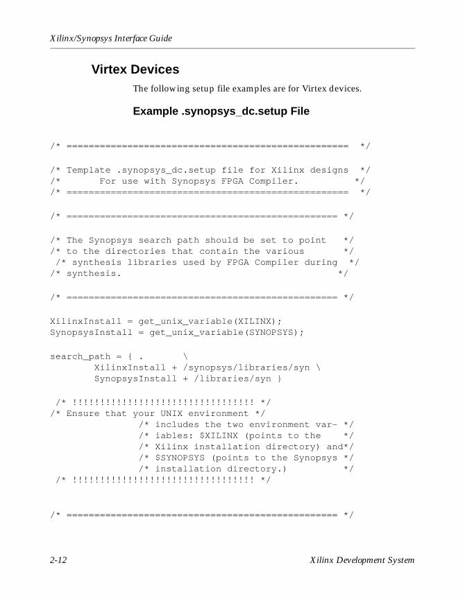
Virtex DevicesThe following setup file examples are for Virtex devices.
Example .synopsys_dc.setup File
/* =================================================== */
/* Template .synopsys_dc.setup file for Xilinx designs *//* For use with Synopsys FPGA Compiler. *//* =================================================== */
/* ================================================= */
/* The Synopsys search path should be set to point *//* to the directories that contain the various */ /* synthesis libraries used by FPGA Compiler during *//* synthesis. */
/* ================================================= */
XilinxInstall = get_unix_variable(XILINX);SynopsysInstall = get_unix_variable(SYNOPSYS);
search_path = { . \ XilinxInstall + /synopsys/libraries/syn \ SynopsysInstall + /libraries/syn }
/* !!!!!!!!!!!!!!!!!!!!!!!!!!!!!!!!! *//* Ensure that your UNIX environment */ /* includes the two environment var- */ /* iables: $XILINX (points to the */ /* Xilinx installation directory) and*/ /* $SYNOPSYS (points to the Synopsys */ /* installation directory.) */ /* !!!!!!!!!!!!!!!!!!!!!!!!!!!!!!!!! */
/* ================================================= */
2-12 Xilinx Development System
Getting Started
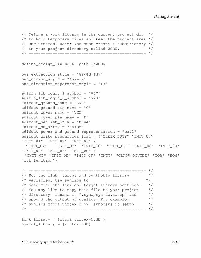
/* Define a work library in the current project dir *//* to hold temporary files and keep the project area *//* uncluttered. Note: You must create a subdirectory *//* in your project directory called WORK. */ /* ================================================= */
define_design_lib WORK -path ./WORK
bus_extraction_style = "%s<%d:%d>"bus_naming_style = "%s<%d>"bus_dimension_separator_style = "><"
edifin_lib_logic_1_symbol = "VCC"edifin_lib_logic_0_symbol = "GND"edifout_ground_name = "GND"edifout_ground_pin_name = "G"edifout_power_name = "VCC"edifout_power_pin_name = "P"edifout_netlist_only = "true"edifout_no_array = "false"edifout_power_and_ground_representation = "cell"edifout_write_properties_list = {"CLK1X_DUTY" "INIT_00" "INIT_01" "INIT_02" "INIT_03" \ "INIT_04" "INIT_05" "INIT_06" "INIT_07" "INIT_08" "INIT_09""INIT_0A" "INIT_0B" "INIT_0C" \ "INIT_0D" "INIT_0E" "INIT_0F" "INIT" "CLKDV_DIVIDE" "IOB" "EQN""lut_function"}
/* ================================================= *//* Set the link, target and synthetic library */ /* variables. Use synlibs to *//* determine the link and target library settings. *//* You may like to copy this file to your project *//* directory, rename it ".synopsys_dc.setup" and */ /* append the output of synlibs. For example: */ /* synlibs xfpga_virtex-3 >> .synopsys_dc.setup *//* ================================================= */
link_library = {xfpga_virtex-5.db }symbol_library = {virtex.sdb}
Xilinx/Synopsys Interface Guide 2-13
Xilinx/Synopsys Interface Guide
define_design_lib xdw_virtex -path XilinxInstall + /synopsys/libraries/dw/lib/virtexsynthetic_library = {xdw_virtex.sldb standard.sldb}
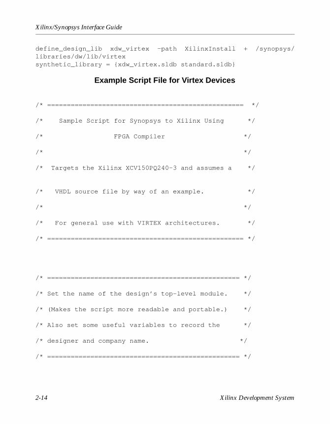
Example Script File for Virtex Devices
/* ================================================== */
/* Sample Script for Synopsys to Xilinx Using */
/* FPGA Compiler */
/* */
/* Targets the Xilinx XCV150PQ240-3 and assumes a */
/* VHDL source file by way of an example. */
/* */
/* For general use with VIRTEX architectures. */
/* ================================================== */
/* ================================================= */
/* Set the name of the design’s top-level module. */
/* (Makes the script more readable and portable.) */
/* Also set some useful variables to record the */
/* designer and company name. */
/* ================================================= */
2-14 Xilinx Development System
Getting Started
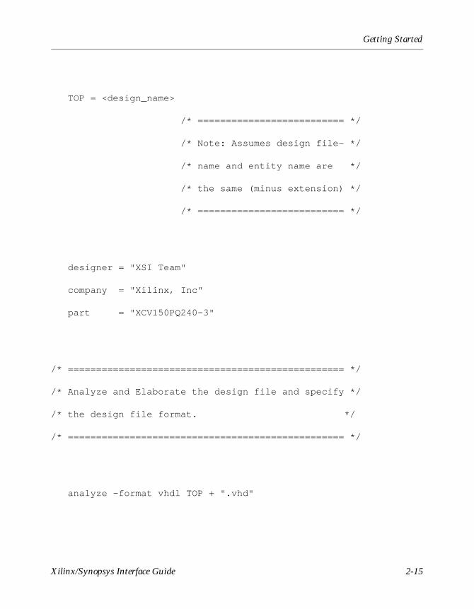
TOP = <design_name>
/* ========================== */
/* Note: Assumes design file- */
/* name and entity name are */
/* the same (minus extension) */
/* ========================== */
designer = "XSI Team"
company = "Xilinx, Inc"
part = "XCV150PQ240-3"
/* ================================================= */
/* Analyze and Elaborate the design file and specify */
/* the design file format. */
/* ================================================= */
analyze -format vhdl TOP + ".vhd"
Xilinx/Synopsys Interface Guide 2-15
Xilinx/Synopsys Interface Guide
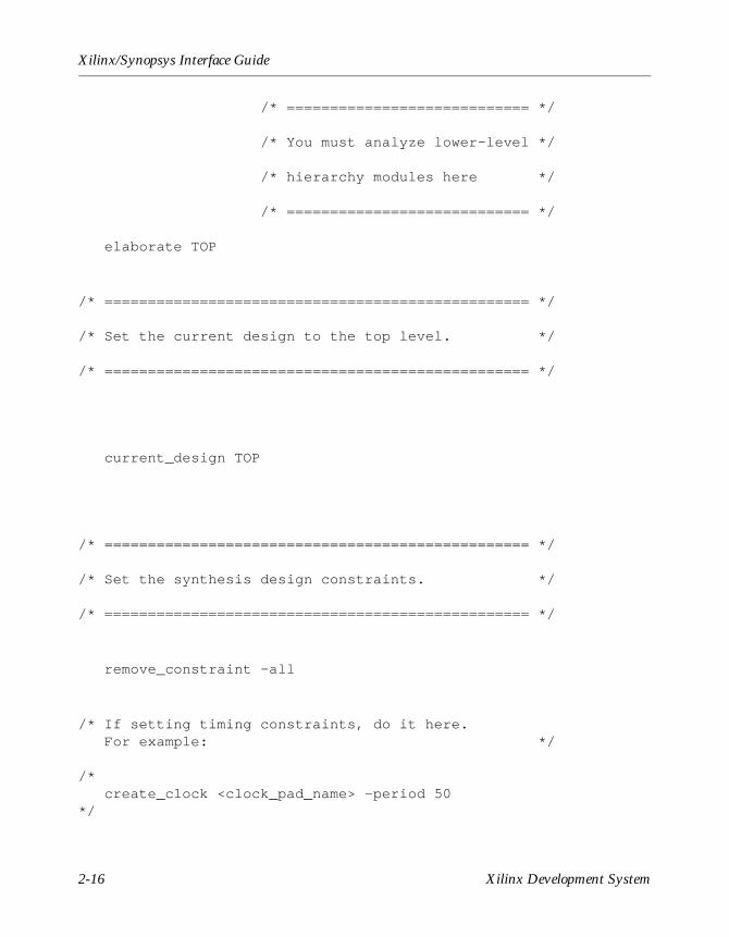
/* ============================ */
/* You must analyze lower-level */
/* hierarchy modules here */
/* ============================ */
elaborate TOP
/* ================================================= */
/* Set the current design to the top level. */
/* ================================================= */
current_design TOP
/* ================================================= */
/* Set the synthesis design constraints. */
/* ================================================= */
remove_constraint -all
/* If setting timing constraints, do it here. For example: */
/* create_clock <clock_pad_name> -period 50*/
2-16 Xilinx Development System
Getting Started
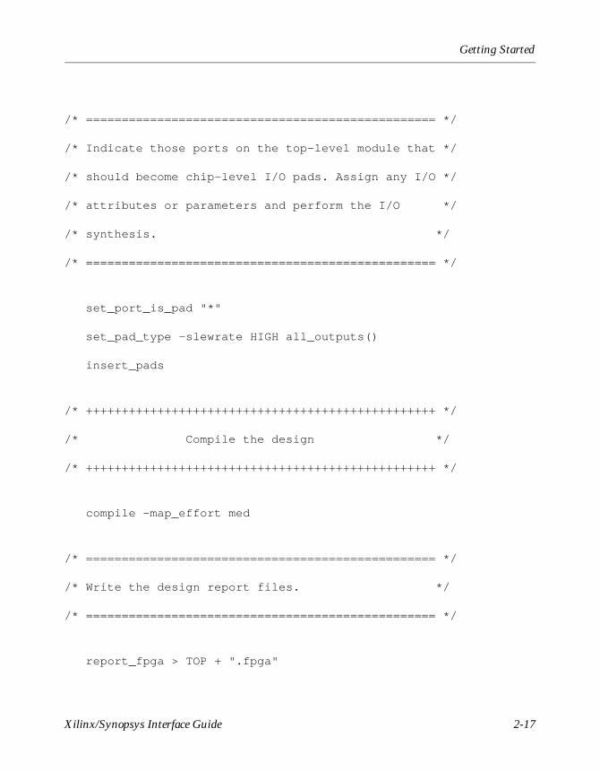
/* ================================================= */
/* Indicate those ports on the top-level module that */
/* should become chip-level I/O pads. Assign any I/O */
/* attributes or parameters and perform the I/O */
/* synthesis. */
/* ================================================= */
set_port_is_pad "*"
set_pad_type -slewrate HIGH all_outputs()
insert_pads
/* +++++++++++++++++++++++++++++++++++++++++++++++++ */
/* Compile the design */
/* +++++++++++++++++++++++++++++++++++++++++++++++++ */
compile -map_effort med
/* ================================================= */
/* Write the design report files. */
/* ================================================= */
report_fpga > TOP + ".fpga"
Xilinx/Synopsys Interface Guide 2-17
Xilinx/Synopsys Interface Guide
report_timing > TOP + ".timing"
/* ================================================= */
/* Set the part type for the output netlist. */
/* ================================================= */
set_attribute TOP "part" -type string part
/* ================================================= */
/* Save design in EDIF format as <design>.sedif */
/* ================================================= */
write -format xnf -hierarchy -output TOP + ".sedif"
/* ================================================= */
/* Write out the design to a DB. */
/* ================================================= */
write -format db -hierarchy -output TOP + ".db"
/* ================================================= */
/* Write-out the timing constraints that were */
/* applied earlier. (Note that any design hierarchy */
/* needs to be flattened before the constraints are */
2-18 Xilinx Development System
Getting Started
/* written-out.) */
/* ================================================= */
write_script > TOP + ".dc"
/* ================================================= */
/* Call the Synopsys-to-Xilinx constraints translator*/
/* utility DC2NCF to convert the Synopsys constraints*/
/* to a Xilinx NCF file. You may like to view */
/* dc2ncf.log to review the translation process. */
/* ================================================= */
sh dc2ncf -w TOP + ".dc"
/* ================================================= */
/* Exit the Compiler. */
/* ================================================= */
exit
/* ================================================= */
/* Now run the Xilinx design implementation tools. */
/* ================================================= */
Xilinx/Synopsys Interface Guide 2-19
Xilinx/Synopsys Interface Guide
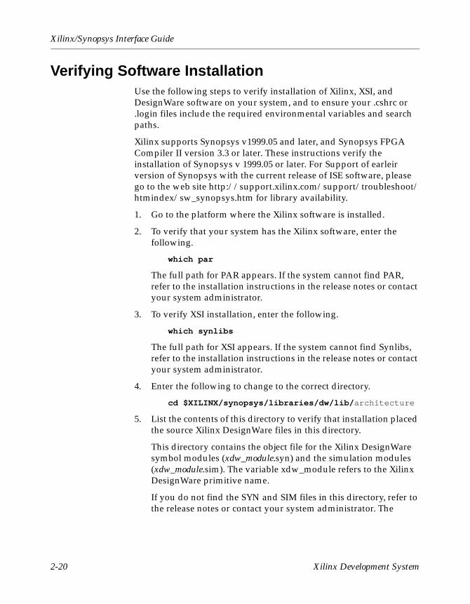
Verifying Software InstallationUse the following steps to verify installation of Xilinx, XSI, and DesignWare software on your system, and to ensure your .cshrc or .login files include the required environmental variables and search paths.
Xilinx supports Synopsys v1999.05 and later, and Synopsys FPGA Compiler II version 3.3 or later. These instructions verify the installation of Synopsys v 1999.05 or later. For Support of earleir version of Synopsys with the current release of ISE software, please go to the web site http://support.xilinx.com/support/troubleshoot/htmindex/sw_synopsys.htm for library availability.
1. Go to the platform where the Xilinx software is installed.
2. To verify that your system has the Xilinx software, enter the following.
which par
The full path for PAR appears. If the system cannot find PAR, refer to the installation instructions in the release notes or contact your system administrator.
3. To verify XSI installation, enter the following.
which synlibs
The full path for XSI appears. If the system cannot find Synlibs, refer to the installation instructions in the release notes or contact your system administrator.
4. Enter the following to change to the correct directory.
cd $XILINX/synopsys/libraries/dw/lib/architecture
5. List the contents of this directory to verify that installation placed the source Xilinx DesignWare files in this directory.
This directory contains the object file for the Xilinx DesignWare symbol modules (xdw_module.syn) and the simulation modules (xdw_module.sim). The variable xdw_module refers to the Xilinx DesignWare primitive name.
If you do not find the SYN and SIM files in this directory, refer to the release notes or contact your system administrator. The
2-20 Xilinx Development System
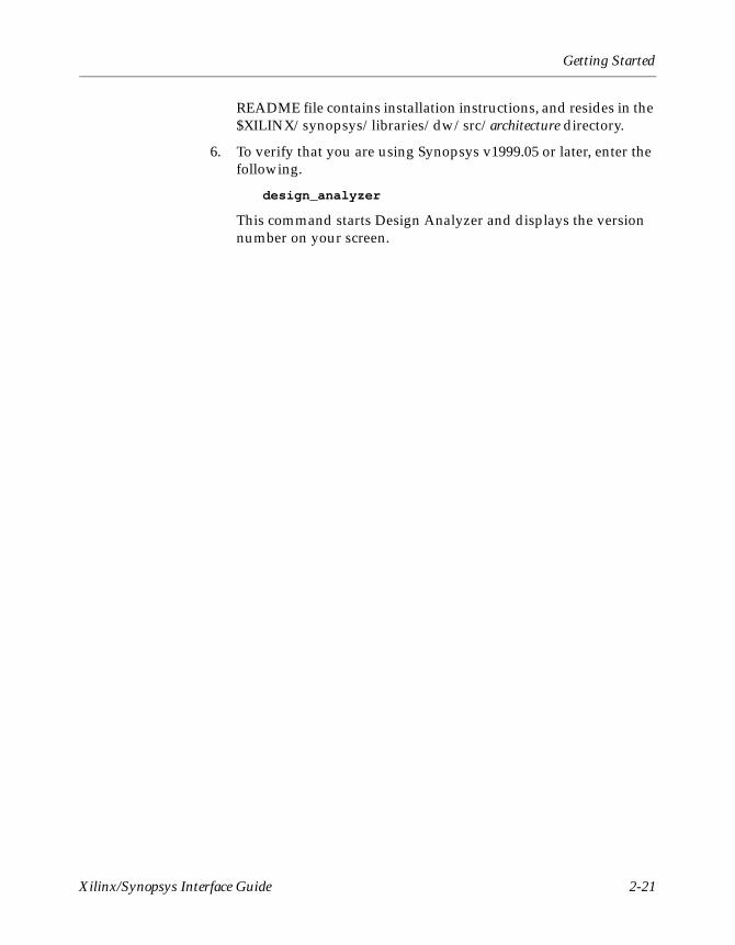
Getting Started
README file contains installation instructions, and resides in the $XILINX/synopsys/libraries/dw/src/architecture directory.
6. To verify that you are using Synopsys v1999.05 or later, enter the following.
design_analyzer
This command starts Design Analyzer and displays the version number on your screen.
Xilinx/Synopsys Interface Guide 2-21

Xilinx/Synopsys Interface Guide
2-22 Xilinx Development System
Chapter 3
Synthesizing Your Design with FPGA Compiler II
Synthesize and implement your HDL designs for Xilinx FPGA devices with FPGA Compiler II by using the information in the following sections.
• “Before You Begin”
• “Naming Conventions”
• “Porting Code from FPGA Compiler to FPGA Compiler II”
• “Converting Script Files from FPGA Compiler and Design Compiler”
• “Synthesizing the Design”
• “Entering Design Constraints and Controls”
• “Specifying Timing Constraints”
• “Optimizing a Design Implementation”
• “Evaluating Timing Delays”
• “Exporting the Netlist”
• “Using the Xilinx Development System”
• “HDL Coding Techniques”
• “Inserting Bidirectional I/Os”
• “Implementing 3-State Registered Output”
• “Attribute Passing”
• “Implementing Clock Buffers”
• “Using Memory”
Xilinx/Synopsys Interface Guide 3-1
Xilinx/Synopsys Interface Guide
• “Performing Boundary Scan”
• “Using the Global Set/Reset Net”
Before You BeginBefore beginning a Xilinx design using the Synopsys tools, read the “Getting Started” chapter and ensure the following.
• Verify the installation of Xilinx software on your system.
• Verify that you use Synopsys version 3.3.1 or later for FPGA Compiler II.
Naming ConventionsUnless otherwise noted, the following naming conventions are used to group Xilinx device families:
• Virtex represents Virtex, Virtex-E, Virtex-II and Spartan-II devices.
• Spartan represents Spartan and SpartanXL devices.
• XC4000 represents XC4000E, XC4000L, XC4000EX, XC4000XL, XC4000XLA and XC4000XV devices.
• XC9500 represents XC9500, XC9500XL, XC9500XV and XC9500XVA devices.
• XC3000 represents XC3100 and XC3100A devices.
• XC5200 represents XC5200 devices.
Porting Code from FPGA Compiler to FPGA Compiler II
You can port a design from FPGA Compiler or Design Compiler to FPGA Compiler II. You do not have to modify the code if you are compiling a 100 percent behavioral design originally compiled with FPGA Compiler or Design Compiler. However, if you instantiated components from the XSI libraries, understand that some of these components do not exist in the FPGA Compiler II libraries.
3-2 Xilinx Development System
Synthesizing Your Design with FPGA Compiler II
Some of the components you can instantiate in the Xilinx design flow you cannot instantiate in the FPGA Compiler II tool because of slight differences in names. For example, the BUFGP_F in the XSI component library does not exist in the FPGA Compiler II component library. In FPGA Compiler II, the equivalent name of the BUFGP_F is BUFGP. For a complete listing of the library cells that can be instantiated in FPGA Compiler II, refer to the contents of the following.
fpgacompilerII/lib/virtex
fpgacompilerII/lib/spartan
fpgacompilerII/lib/spartanxl
fpgacompilerII/lib/xc4000e
fpgacompilerII/lib/xc4000ex
fpgacompilerII/lib/xc9500
fpgacompilerII/lib/xc3000
fpgacompilerII/lib/xc5200
The fpgacompilerII directory is where FPGA Compiler II resides on your system. These directories contain files with a .dsn extension. The string in front of .dsn is the name of the CELL that you can instantiate in FPGA Compiler. Refer to the Xilinx Libraries Guide for pin names.
In general, instantiation is not necessary. For the XC4000 and Virtex FPGA Compiler II flow, you must instantiate the following components.
• I/O multiplexers
• Fast capture latches
• RAM
• BSCAN, READBACK
• LogiBLOX, CoreGen modules
Converting Script Files from FPGA Compiler and Design Compiler
This chapter will not document the TCL-based scripting capabilities of FPGA Compiler II. Please consult the FPGA Compiler II
Xilinx/Synopsys Interface Guide 3-3
Xilinx/Synopsys Interface Guide
documentation for details on the fc2_shell program. However, a few things are noted here:
• fc2_shell is the command line name of the FPGA Compiler II shell tool.
• A script converter, dc-transcript, is available on Unix to convert DC shell scripts to TCL shell. This program is not available within FPGA Compiler II itself.
• TCL script can be created after synthesizing in the FPGA Compiler II GUI. Select the optimized chip and then select Script → Export FPGA Script to create a script of all the commands run up to that point.
Synthesizing the DesignThis section describes the synthesis flow through the FPGA Compiler II product, using the Graphical User Interface (GUI), from creating the project through the netlist generation.
After opening the FPGA Compiler II GUI, select File → New Project. Select the name and location for this project before clicking Create. HDL source files may also be added at this time.
3-4 Xilinx Development System
Synthesizing Your Design with FPGA Compiler II
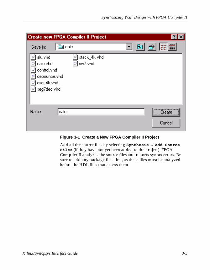
Figure 3-1 Create a New FPGA Compiler II Project
Add all the source files by selecting Synthesis → Add Source Files (if they have not yet been added to the project). FPGA Compiler II analyzes the source files and reports syntax errors. Be sure to add any package files first, as these files must be analyzed before the HDL files that access them.
Xilinx/Synopsys Interface Guide 3-5
Xilinx/Synopsys Interface Guide
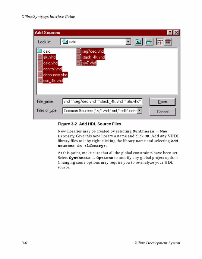
Figure 3-2 Add HDL Source Files
New libraries may be created by selecting Synthesis → New Library. Give this new library a name and click OK. Add any VHDL library files to it by right clicking the library name and selecting Add sources in <library>.
At this point, make sure that all the global constraints have been set. Select Synthesis → Options to modify any global project options. Changing some options may require you to re-analyze your HDL source.
3-6 Xilinx Development System
Synthesizing Your Design with FPGA Compiler II
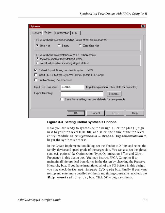
Figure 3-3 Setting Global Synthesis Options
Now you are ready to synthesize the design. Click the plus (+) sign next to your top level HDL file, and select the name of the top level entity/module. Select Synthesis → Create Implementation to begin the synthesis process.
In the Create Implementation dialog, set the Vendor to Xilinx and select the family, device and speed grade of the target chip. You can also set the global synthesis options like Optimization Type, Optimization Effort and Clock Frequency in this dialog box. You may instruct FPGA Compiler II to maintain all hierarchical boundaries in the design by checking the Preserve Hierarchy box. If you have instantiated all of the I/O buffers in this design, you may check the Do not insert I/O pads box. Finally, if you want to stop and enter more detailed synthesis and timing constraints, uncheck the Skip constraint entry box. Click OK to begin synthesis.
Xilinx/Synopsys Interface Guide 3-7
Xilinx/Synopsys Interface Guide
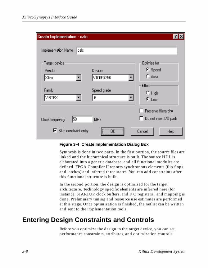
Figure 3-4 Create Implementation Dialog Box
Synthesis is done in two parts. In the first portion, the source files are linked and the hierarchical structure is built. The source HDL is elaborated into a generic database, and all functional modules are defined. FPGA Compiler II reports synchronous elements (flip flops and latches) and inferred three states. You can add constraints after this functional structure is built.
In the second portion, the design is optimized for the target architecture. Technology specific elements are inferred here (for instance, STARTUP, clock buffers, and I/O registers), and mapping is done. Preliminary timing and resource use estimates are performed at this stage. Once optimization is finished, the netlist can be written and sent to the implementation tools.
Entering Design Constraints and ControlsBefore you optimize the design to the target device, you can set performance constraints, attributes, and optimization controls.
3-8 Xilinx Development System
Synthesizing Your Design with FPGA Compiler II
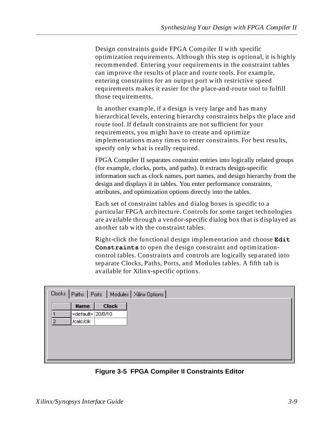
Design constraints guide FPGA Compiler II with specific optimization requirements. Although this step is optional, it is highly recommended. Entering your requirements in the constraint tables can improve the results of place and route tools. For example, entering constraints for an output port with restrictive speed requirements makes it easier for the place-and-route tool to fulfill those requirements.
In another example, if a design is very large and has many hierarchical levels, entering hierarchy constraints helps the place and route tool. If default constraints are not sufficient for your requirements, you might have to create and optimize implementations many times to enter constraints. For best results, specify only what is really required.
FPGA Compiler II separates constraint entries into logically related groups (for example, clocks, ports, and paths). It extracts design-specific information such as clock names, port names, and design hierarchy from the design and displays it in tables. You enter performance constraints, attributes, and optimization options directly into the tables.
Each set of constraint tables and dialog boxes is specific to a particular FPGA architecture. Controls for some target technologies are available through a vendor-specific dialog box that is displayed as another tab with the constraint tables.
Right-click the functional design implementation and choose Edit Constraints to open the design constraint and optimization-control tables. Constraints and controls are logically separated into separate Clocks, Paths, Ports, and Modules tables. A fifth tab is available for Xilinx-specific options.
Figure 3-5 FPGA Compiler II Constraints Editor
Xilinx/Synopsys Interface Guide 3-9
Xilinx/Synopsys Interface Guide
The contents of the tables depend on the architecture that you chose. Notice that clock and pad tabs are preloaded with the clock frequency (and corresponding period) that you entered for the base clock frequency.
After entering constraint, attribute, and option information, close the implementation’s constraint window. This will save your changes.
Specifying Timing ConstraintsThe timing constraints issued to Synopsys to control the synthesis process pass through the design implementation tools to control the place and route process. To get the best possible results, make these constraints realistic and achievable.
During the synthesis of your design, area and timing constraints can impact implementation almost as much as changes made to your HDL code. Carefully apply area and timing constraints. During the implementation of your design, timing constraints have a direct impact on run time and performance verification. For example, the run time required to find a place and route solution to support the 40 MHz operation of a design takes longer than that required to find a 4 MHz solution. Meaningful and detailed timing constraints also allow the design implementation tools to report the status of your design’s timing in terms of your timing goals.
After creating a chip, but before optimization, edit the chip by entering timing constraints. FPGA Compiler II lets you enter timing constraints for common types of paths including pad-to-pad, pad-to-setup, register-to-register, and clock-to output paths. FPGA Compiler II compares these timing constraints to the values calculated by its built-in Time Tracker.
You enter timing constraints in a top-down method: starting with global constraints (such as clock periods), proceeding to the more specific (such as group path timing), then to the most specific (input and output delay).
The following procedure shows you how to enter timing specification for your design in FPGA Compiler II.
1. In the Clocks constraint table, enter the default clock waveform for each clock in your design, including the clock period and rise and fall times.
The clock default is the first row in the Clock constraint table. The default should be sufficient in most of the cases when the circuit
3-10 Xilinx Development System
Synthesizing Your Design with FPGA Compiler II
has only clock, and there are no special input delay and output delay requirements.
The waveform you define using the Define command in the Clock pulldown list in the Clocks constraint table should be sufficient for most synchronous circuits without special I/O port delay requirements and without multicycle paths.
2. In the Paths constraint table, change the default path delays that FPGA Compiler II automatically calculates from the clock waveform.
When there are more restrictive timing requirements than the defaults, you can override a default path constraint with a more specific constraint by entering path constraints in the Paths constraint table. Here you apply timing constraints to groups of paths, the set of all clock-to output paths, for example. The input and output delays for the I/O ports are given default values based on the path constraints. It is important that the delays be specified accurately so that they do not overconstrain or underconstrain the optimization.
3. In the Ports constraint table, change the default input delay and output delay of I/O ports when they have special requirements. Any delay specified at a port overrides the path delay from or to the port.
Sometimes a single value applied to many paths is not sufficient for a particular port. In the example of clock-to-out paths, there may be a particular output port that has a more restrictive clock-to-output requirement. To override a path constraint with an even more specific constraint, proceed to the Ports constraint table, where you can set input and output delays for individual ports.
After entering timing constraints, optimize the design.
Specifying Clock ConstraintsUse the Clock constraint table to specify the waveforms of periodic signals in the design. FPGA Compiler II displays the constraint tables when you click the right mouse button on an implementation icon and select Edit Constraints.
FPGA Compiler II automatically constructs the list of periodic signals when it creates an implementation. For each periodic signal, FPGA
Xilinx/Synopsys Interface Guide 3-11
Xilinx/Synopsys Interface Guide
Compiler II displays the name (Name column) and period/rise/fall waveform (Clock column).
• Name
The full name of the periodic signal in the design hierarchy (for example, top/module1/clk).
• Clock
The waveform (period, rise time, fall time) of each periodic signal. Note that the falling edge can be first, and the clock’s duty cycle does not have to be 50%. To specify a waveform, click the Clock cell, click the expand arrow that appears in the cell, and then select Define...This displays the Define Clock dialog box where you can enter the period, rise time, and fall time of the signal. The waveform in this dialog box is for information only and does not reflect the values you enter. Alternatively, you can click the expand arrow in the cell and select a set of values from the list. This list contains all the previously entered values. You can also use the cut and paste commands.
• Default Timing Values
When a table cell is blank, FPGA Compiler II uses the default clock waveform defined in the first row. This default waveform is derived from the Clock frequency value in the Create Implementation dialog box. You can override this value when editing the implementation constraints.
The following procedure describes the steps to specify clock constraints.
1. Open the Clocks constraint table in the Chips window by selecting the preoptimized chip, clicking the right mouse button, and selecting Edit Constraints.
2. Specify the waveforms of periodic signals in the design. To specify a waveform, click the Clock column cell and then the expand arrow appearing in the cell.
3. Select Define.
The Define Clock dialog box appears, where you can enter the period, rise time, and fall time of the signal.
3-12 Xilinx Development System
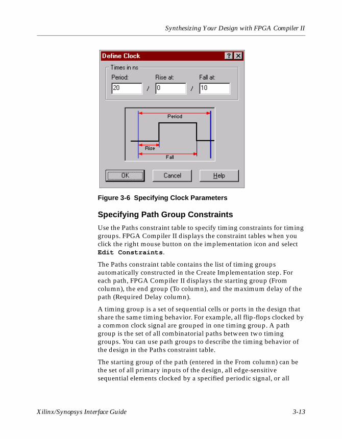
Synthesizing Your Design with FPGA Compiler II
Figure 3-6 Specifying Clock Parameters
Specifying Path Group Constraints
Use the Paths constraint table to specify timing constraints for timing groups. FPGA Compiler II displays the constraint tables when you click the right mouse button on the implementation icon and select Edit Constraints.
The Paths constraint table contains the list of timing groups automatically constructed in the Create Implementation step. For each path, FPGA Compiler II displays the starting group (From column), the end group (To column), and the maximum delay of the path (Required Delay column).
A timing group is a set of sequential cells or ports in the design that share the same timing behavior. For example, all flip-flops clocked by a common clock signal are grouped in one timing group. A path group is the set of all combinatorial paths between two timing groups. You can use path groups to describe the timing behavior of the design in the Paths constraint table.
The starting group of the path (entered in the From column) can be the set of all primary inputs of the design, all edge-sensitive sequential elements clocked by a specified periodic signal, or all
Xilinx/Synopsys Interface Guide 3-13
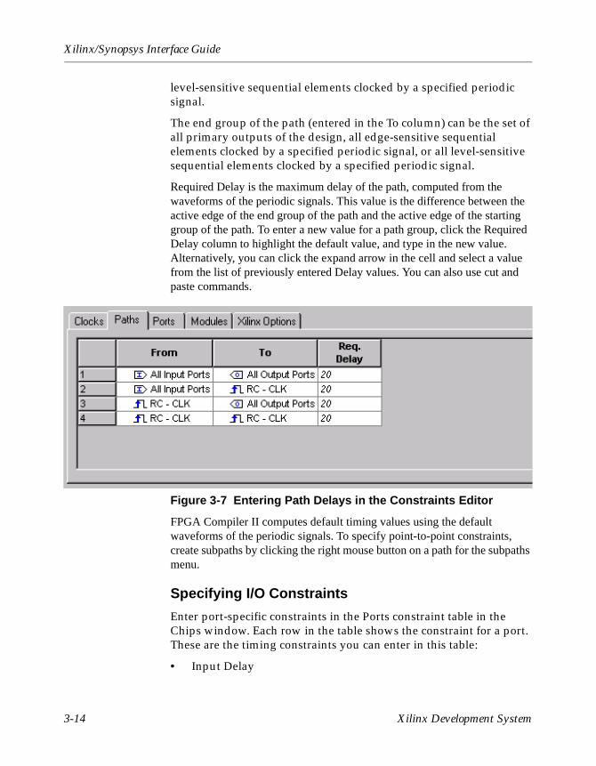
Xilinx/Synopsys Interface Guide
level-sensitive sequential elements clocked by a specified periodic signal.
The end group of the path (entered in the To column) can be the set of all primary outputs of the design, all edge-sensitive sequential elements clocked by a specified periodic signal, or all level-sensitive sequential elements clocked by a specified periodic signal.
Required Delay is the maximum delay of the path, computed from the waveforms of the periodic signals. This value is the difference between the active edge of the end group of the path and the active edge of the starting group of the path. To enter a new value for a path group, click the Required Delay column to highlight the default value, and type in the new value. Alternatively, you can click the expand arrow in the cell and select a value from the list of previously entered Delay values. You can also use cut and paste commands.
Figure 3-7 Entering Path Delays in the Constraints Editor
FPGA Compiler II computes default timing values using the default waveforms of the periodic signals. To specify point-to-point constraints, create subpaths by clicking the right mouse button on a path for the subpaths menu.
Specifying I/O Constraints
Enter port-specific constraints in the Ports constraint table in the Chips window. Each row in the table shows the constraint for a port. These are the timing constraints you can enter in this table:
• Input Delay
3-14 Xilinx Development System
Synthesizing Your Design with FPGA Compiler II
The input delay of an input or inout port is the maximum delay from that port to a timing group. To define an input delay, click the Input Delay cell for a port, and select Define. In the Define Delay dialog box, define the input delay.
• Output Delay
The output delay of an output or inout port is the maximum delay from a timing group to that port. To define an output delay, click the Output Delay cell for a port and select Define. In the Define Delay dialog box, define the output delay.
• Pad Location
You can specify the location of pads for a port. You cannot specify pad locations for a design that has the Do Not Insert I/O Pads option selected.
Timing Subpaths
With FPGA Compiler II, you can enter point-to-point constraints (for instance, multicycle timing paths) by creating subpaths. The procedure to create subpaths for a path follows.
1. Right-click on the path in the Paths table.
The selections are New Subpath, Edit Subpath, and Delete Subpath.
2. Select New Subpath or Edit Subpath (if one has already been created).
The Create/Edit Timing Sub Path dialog box opens, displaying the primary path and the components in that path.
3. Enter a name for the subpath.
4. Select startpoints and endpoints for each subpath group by double-clicking the object icons. The names of subpath groups must be unique.
5. Specify the delay for the subpath. You can specify a different constraint for each subpath.
You can use the Select All buttons to make multiple startpoint and endpoint selections. You can use the Clear all buttons to clear all startpoint and endpoint selections. You can enter common expressions such as DI* to make multiple selections.
Xilinx/Synopsys Interface Guide 3-15
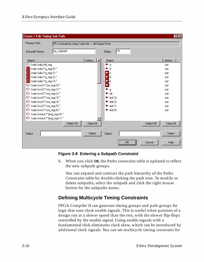
Xilinx/Synopsys Interface Guide
Figure 3-8 Entering a Subpath Constraint
6. When you click OK, the Paths constraint table is updated to reflect the new subpath groups.
You can expand and contract the path hierarchy of the Paths Constraint table by double-clicking the path icon. To modify or delete subpaths, select the subpath and click the right mouse button for the subpaths menu.
Defining Multicycle Timing Constraints
FPGA Compiler II can generate timing groups and path groups for logic that uses clock enable signals. This is useful when portions of a design run at a slower speed than the rest, with the slower flip-flops controlled by the enable signal. Using enable signals with a fundamental click eliminates clock skew, which can be introduced by additional clock signals. You can set multicycle timing constraint for
3-16 Xilinx Development System
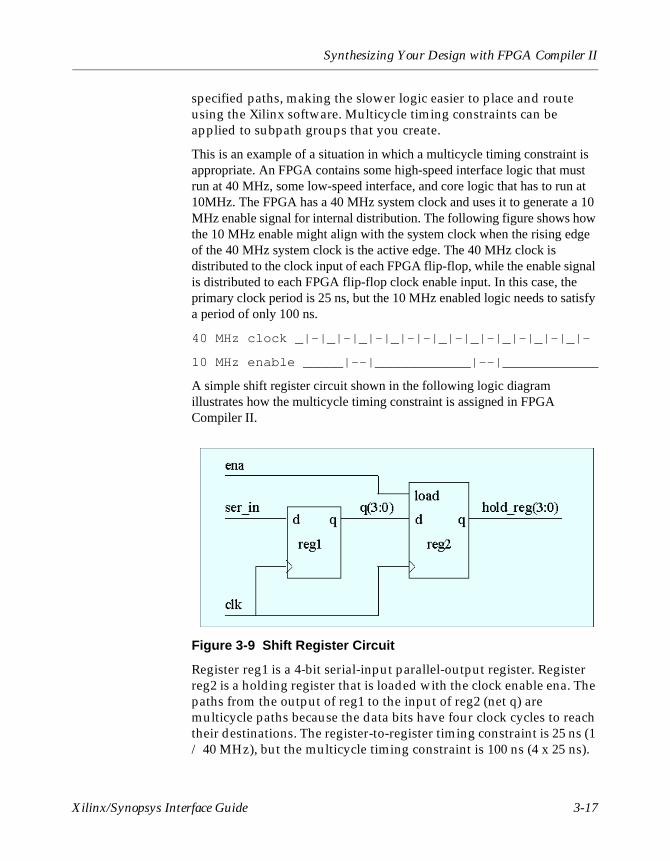
Synthesizing Your Design with FPGA Compiler II
specified paths, making the slower logic easier to place and route using the Xilinx software. Multicycle timing constraints can be applied to subpath groups that you create.
This is an example of a situation in which a multicycle timing constraint is appropriate. An FPGA contains some high-speed interface logic that must run at 40 MHz, some low-speed interface, and core logic that has to run at 10MHz. The FPGA has a 40 MHz system clock and uses it to generate a 10 MHz enable signal for internal distribution. The following figure shows how the 10 MHz enable might align with the system clock when the rising edge of the 40 MHz system clock is the active edge. The 40 MHz clock is distributed to the clock input of each FPGA flip-flop, while the enable signal is distributed to each FPGA flip-flop clock enable input. In this case, the primary clock period is 25 ns, but the 10 MHz enabled logic needs to satisfy a period of only 100 ns.
40 MHz clock _|-|_|-|_|-|_|-|-|_|-|_|-|_|-|_|-|_|-
10 MHz enable _____|--|____________|--|____________
A simple shift register circuit shown in the following logic diagram illustrates how the multicycle timing constraint is assigned in FPGA Compiler II.
Figure 3-9 Shift Register Circuit
Register reg1 is a 4-bit serial-input parallel-output register. Register reg2 is a holding register that is loaded with the clock enable ena. The paths from the output of reg1 to the input of reg2 (net q) are multicycle paths because the data bits have four clock cycles to reach their destinations. The register-to-register timing constraint is 25 ns (1 / 40 MHz), but the multicycle timing constraint is 100 ns (4 x 25 ns).
Xilinx/Synopsys Interface Guide 3-17
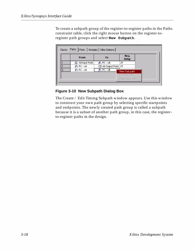
Xilinx/Synopsys Interface Guide
To create a subpath group of the register-to-register paths in the Paths constraint table, click the right mouse button on the register-to-register path groups and select New Subpath.
Figure 3-10 New Subpath Dialog Box
The Create / Edit Timing Subpath window appears. Use this window to construct your own path group by selecting specific startpoints and endpoints. The newly created path group is called a subpath because it is a subset of another path group, in this case, the register-to-register paths in the design.
3-18 Xilinx Development System
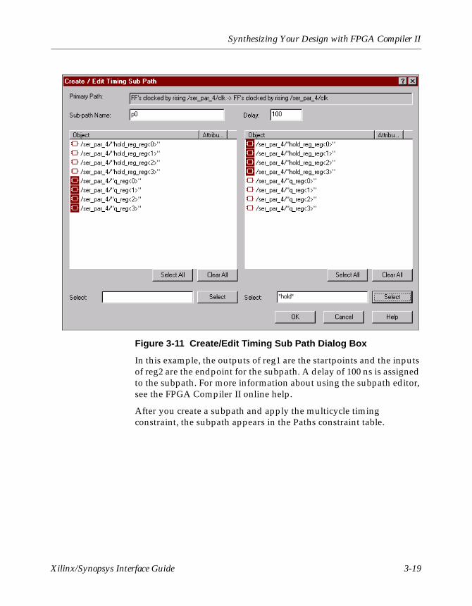
Synthesizing Your Design with FPGA Compiler II
Figure 3-11 Create/Edit Timing Sub Path Dialog Box
In this example, the outputs of reg1 are the startpoints and the inputs of reg2 are the endpoint for the subpath. A delay of 100 ns is assigned to the subpath. For more information about using the subpath editor, see the FPGA Compiler II online help.
After you create a subpath and apply the multicycle timing constraint, the subpath appears in the Paths constraint table.
Xilinx/Synopsys Interface Guide 3-19
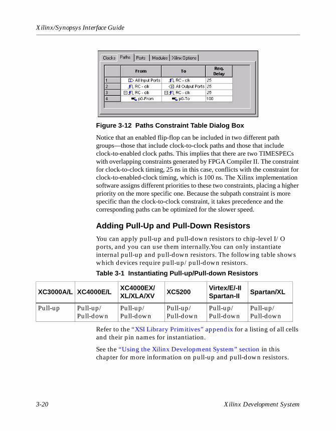
Xilinx/Synopsys Interface Guide
Figure 3-12 Paths Constraint Table Dialog Box
Notice that an enabled flip-flop can be included in two different path groups—those that include clock-to-clock paths and those that include clock-to-enabled clock paths. This implies that there are two TIMESPECs with overlapping constraints generated by FPGA Compiler II. The constraint for clock-to-clock timing, 25 ns in this case, conflicts with the constraint for clock-to-enabled-clock timing, which is 100 ns. The Xilinx implementation software assigns different priorities to these two constraints, placing a higher priority on the more specific one. Because the subpath constraint is more specific than the clock-to-clock constraint, it takes precedence and the corresponding paths can be optimized for the slower speed.
Adding Pull-Up and Pull-Down Resistors
You can apply pull-up and pull-down resistors to chip-level I/O ports, and you can use them internally.You can only instantiate internal pull-up and pull-down resistors. The following table shows which devices require pull-up/pull-down resistors.
Refer to the “XSI Library Primitives” appendix for a listing of all cells and their pin names for instantiation.
See the “Using the Xilinx Development System” section in this chapter for more information on pull-up and pull-down resistors.
Table 3-1 Instantiating Pull-up/Pull-down Resistors
XC3000A/L XC4000E/LXC4000EX/XL/XLA/XV
XC5200Virtex/E/-II Spartan-II
Spartan/XL
Pull-up Pull-up/Pull-down
Pull-up/Pull-down
Pull-up/Pull-down
Pull-up/Pull-down
Pull-up/Pull-down
3-20 Xilinx Development System
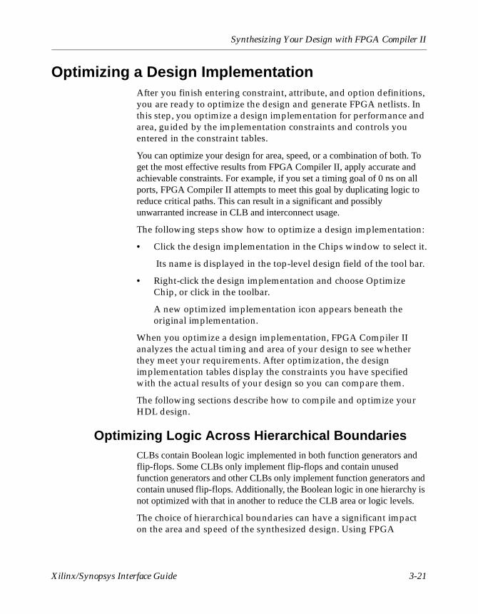
Synthesizing Your Design with FPGA Compiler II
Optimizing a Design ImplementationAfter you finish entering constraint, attribute, and option definitions, you are ready to optimize the design and generate FPGA netlists. In this step, you optimize a design implementation for performance and area, guided by the implementation constraints and controls you entered in the constraint tables.
You can optimize your design for area, speed, or a combination of both. To get the most effective results from FPGA Compiler II, apply accurate and achievable constraints. For example, if you set a timing goal of 0 ns on all ports, FPGA Compiler II attempts to meet this goal by duplicating logic to reduce critical paths. This can result in a significant and possibly unwarranted increase in CLB and interconnect usage.
The following steps show how to optimize a design implementation:
• Click the design implementation in the Chips window to select it.
Its name is displayed in the top-level design field of the tool bar.
• Right-click the design implementation and choose Optimize Chip, or click in the toolbar.
A new optimized implementation icon appears beneath the original implementation.
When you optimize a design implementation, FPGA Compiler II analyzes the actual timing and area of your design to see whether they meet your requirements. After optimization, the design implementation tables display the constraints you have specified with the actual results of your design so you can compare them.
The following sections describe how to compile and optimize your HDL design.
Optimizing Logic Across Hierarchical BoundariesCLBs contain Boolean logic implemented in both function generators and flip-flops. Some CLBs only implement flip-flops and contain unused function generators and other CLBs only implement function generators and contain unused flip-flops. Additionally, the Boolean logic in one hierarchy is not optimized with that in another to reduce the CLB area or logic levels.
The choice of hierarchical boundaries can have a significant impact on the area and speed of the synthesized design. Using FPGA
Xilinx/Synopsys Interface Guide 3-21
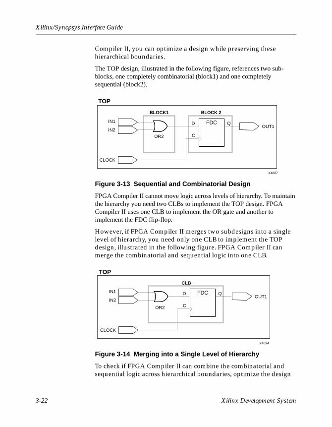
Xilinx/Synopsys Interface Guide
Compiler II, you can optimize a design while preserving these hierarchical boundaries.
The TOP design, illustrated in the following figure, references two sub-blocks, one completely combinatorial (block1) and one completely sequential (block2).
Figure 3-13 Sequential and Combinatorial Design
FPGA Compiler II cannot move logic across levels of hierarchy. To maintain the hierarchy you need two CLBs to implement the TOP design. FPGA Compiler II uses one CLB to implement the OR gate and another to implement the FDC flip-flop.
However, if FPGA Compiler II merges two subdesigns into a single level of hierarchy, you need only one CLB to implement the TOP design, illustrated in the following figure. FPGA Compiler II can merge the combinatorial and sequential logic into one CLB.
Figure 3-14 Merging into a Single Level of Hierarchy
To check if FPGA Compiler II can combine the combinatorial and sequential logic across hierarchical boundaries, optimize the design
OR2
BLOCK 2BLOCK1
TOP
OUT1IN1
IN2
CLOCK
X4887
D QFDC
C
OR2
CLB
TOP
OUT1IN1
IN2
CLOCK
X4894
D QFDC
C
3-22 Xilinx Development System
Synthesizing Your Design with FPGA Compiler II
with and without hierarchy, and then compare the results as described in the following sections.
By default, FPGA Compiler II flattens your design hierarchy. This can be changed at the top level. To preserve or eliminate the hierarchy on a module per module basis, select the implementation, click the right mouse button, and select Edit Constraints. In the Modules table, set the Preserve or Eliminate attribute on the module. The default is Eliminate.
Using a Flattening Optimization Strategy
Flattening eliminates the existing logic structure. In general, you can flatten random control logic because automatic structuring usually improves upon manual structuring. For FPGA designs, flatten designs when the number of CLBs needed to implement a Boolean function seems too high or there are too many logic levels. You probably do not need to flatten regular or highly structured designs such as adders and ALUs designed with an explicit structure.
Flattening works especially well for the FPGA CLB structure because FPGA Compiler II has a built-in optimizer for Boolean logic. This algorithm works efficiently when the structure decomposes sufficiently so that the Boolean logic can map into the CLB function generators.
Setting Port Attributes and ConstraintsYou can enter port-specific constraints in the Ports constraint table in the Chips window. Each row in the table shows the constraints for a port. You can enter the following timing constraints in the Ports constraint table.
• Input Delay
The input delay of an input or inout port is the maximum delay from that port to a timing group. To define an input delay, click the Input Delay cell for a port, and select Define. In the Define Delay dialog box, define the input delay.
• Output Delay
The output delay of an output or inout port is the maximum delay from a timing group to that port. To define an output delay, click the Output Delay cell for a port and select Define. In the Define Delay dialog box, define the output delay.
Xilinx/Synopsys Interface Guide 3-23
Xilinx/Synopsys Interface Guide
• Pad Location
You can specify the location of pads for a port. You cannot specify pad locations for a design that has the Do Not Insert I/O Pads option selected.
See the bidi_reg.vhd and bidi_reg.v examples in the “Viewing the Schematics” section for designs that contain both instantiated I/Os and I/Os inserted using FPGA Compiler II.
Evaluating Timing DelaysThe Synopsys tools report all delays in nanoseconds. The reported delays include logic-level and interconnect delays. Because FPGA Compiler II synthesizes CLBs and IOBs (XC4000 and Spartan devices) or LUTs and flip-flops (XC3000, XC5200, XC9000 and Virtex devices), it reports logic-level delays with a higher degree of accuracy than Design Compiler.
FPGA Compiler II estimates possible interconnect delays on the basis of a net’s fanout. These estimates allow you to evaluate your design’s performance prior to performing place and route. FPGA Compiler II applies the wire-load model only to nets between CLBs and IOBs (XC4000 devices) or between LUTs, I/Os, and flip-flops (XC3000 and XC5200 devices).
After optimization, edit the chip and select View Results to run the FPGA Compiler II TimeTracker. TimeTracker calculates the delay.
Timing analysis follows the same top-down paradigm (from global to specific) as timing constraint entry. (See the “Specifying Timing Constraints” section of this chapter:.)
The Clocks table contains a new column showing the actual clock frequency for each clock in your design next to the desired frequency derived from your timing constraints. If a particular clock fails to meet its constraint, it is highlighted in red. To see greater detail, proceed to the Paths constraint table.
The Paths constraint table shows the paths that violate a timing constraint and shows a detailed list of each path’s structure.
The Paths table contains an additional column displaying path delay with violations in red. It shows which groups of paths fail to meet constraints. Selecting any particular group lists all paths in that group with their startpoints, endpoints, and delays. At another level of detail, it shows exactly which paths are in violation. Selecting any particular path displays a listing of the composition of the entire path from startpoint to endpoint, including
3-24 Xilinx Development System
Synthesizing Your Design with FPGA Compiler II
each instance in the path, the type of component, the cumulative delay through each instance, and the fanout of that particular pin of the instance.
These tables should provide the information you need to make design improvements without running the implementation tools.
Timing analysis fits into the present FPGA Compiler II design flow and gives you detailed information about the timing behavior of your design. With timing analysis, you can see the actual delay values presented next to the desired delay values. For any path, the TimeTracker provides a detailed listing of the path composition to help you debug critical paths. FPGA Compiler II timing analysis shortens the design cycle by eliminating the need to run implementation tools to get timing information.
Using the FPGA Compiler II Time TrackerThe FPGA Compiler II TimeTracker speeds the design cycle by allowing you to identify and repair critical portions of your design without having to run vendor tools to perform place and route. The TimeTracker is integrated into the existing design flow and runs when you view the results of an optimized chip. It allows you to compare actual delay values to entered constraints.
Timing Analysis also provides details of particular paths and a detailed listing of critical paths.
After you read the HDL source code into FPGA Compiler II and enter timing requirements, synthesize the design for the target FPGA architecture. Then, instead of using FPGA vendor tools to place and route the design, view the results of the optimized chip.
These are the advantages of using the FPGA Compiler II TimeTracker:
• It gives feedback about how you meet your timing requirements without you having to run the vendor’s place and route tool and timing analyzer.
• It presents timing analysis results and timing requirements in a table, making the results easy to interpret.
Xilinx/Synopsys Interface Guide 3-25
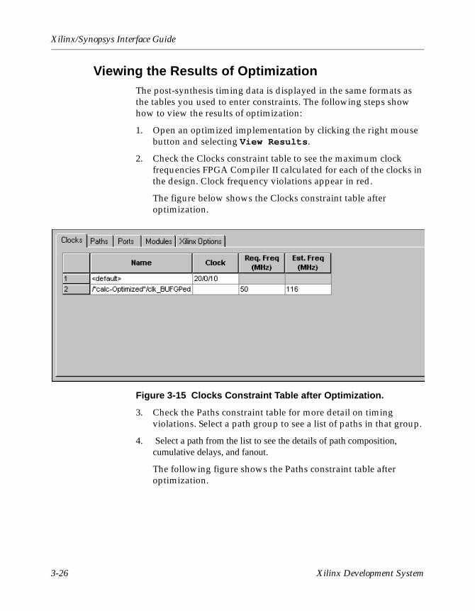
Xilinx/Synopsys Interface Guide
Viewing the Results of OptimizationThe post-synthesis timing data is displayed in the same formats as the tables you used to enter constraints. The following steps show how to view the results of optimization:
1. Open an optimized implementation by clicking the right mouse button and selecting View Results.
2. Check the Clocks constraint table to see the maximum clock frequencies FPGA Compiler II calculated for each of the clocks in the design. Clock frequency violations appear in red.
The figure below shows the Clocks constraint table after optimization.
Figure 3-15 Clocks Constraint Table after Optimization.
3. Check the Paths constraint table for more detail on timing violations. Select a path group to see a list of paths in that group.
4. Select a path from the list to see the details of path composition, cumulative delays, and fanout.
The following figure shows the Paths constraint table after optimization.
3-26 Xilinx Development System
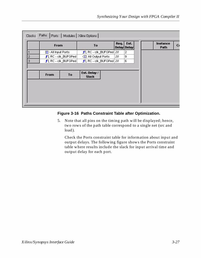
Synthesizing Your Design with FPGA Compiler II
Figure 3-16 Paths Constraint Table after Optimization.
5. Note that all pins on the timing path will be displayed; hence, two rows of the path table correspond to a single net (src and load).
Check the Ports constraint table for information about input and output delays. The following figure shows the Ports constraint table where results include the slack for input arrival time and output delay for each port.
Xilinx/Synopsys Interface Guide 3-27
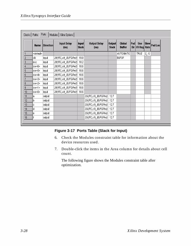
Xilinx/Synopsys Interface Guide
Figure 3-17 Ports Table (Slack for Input)
6. Check the Modules constraint table for information about the device resources used.
7. Double-click the items in the Area column for details about cell count.
The following figure shows the Modules constraint table after optimization.
3-28 Xilinx Development System
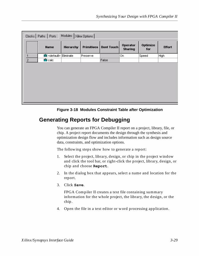
Synthesizing Your Design with FPGA Compiler II
Figure 3-18 Modules Constraint Table after Optimization
Generating Reports for DebuggingYou can generate an FPGA Compiler II report on a project, library, file, or chip. A project report documents the design through the synthesis and optimization design flow and includes information such as design source data, constraints, and optimization options.
The following steps show how to generate a report:
1. Select the project, library, design, or chip in the project window and click the tool bar, or right-click the project, library, design, or chip and choose Report.
2. In the dialog box that appears, select a name and location for the report.
3. Click Save.
FPGA Compiler II creates a text file containing summary information for the whole project, the library, the design, or the chip.
4. Open the file in a text editor or word processing application.
Xilinx/Synopsys Interface Guide 3-29
Xilinx/Synopsys Interface Guide
Viewing the SchematicsFPGA Compiler II creates schematic representations of the logic it synthesizes. To view a schematic, right click on either the functional structure or the optimized structure in the Chips window and select View Schematic. Use the items in the View Toolbar to navigate within the schematics.
Exporting the NetlistThe Export Netlist button opens the Export Netlist dialog box. You export the selected optimized design for place-and-route.The netlists are automatically formatted into Electronic Data Interchange Format (EDIF). You can specify the export design directory. Individual file names correspond to the source design names.
You can also export Verilog or VHDL netlists for functional simulation along with the design netlist. FPGA Compiler II passes the timing constraints with the netlist.Timing constraints are not included in the netlist file for any design that you compiled with the Do Not Insert I/O Pads option selected.
Timing constraints can also be exported by checking the Export Timing Specifications checkbox.
The option labeled Bus Style in the Place and Route section of the Export dialog box adds control to the bus style for EDIF output. Bus information for top-level I/O can be preserved or eliminated.
The default setting, Expand, causes each bit of a bus to become an individual I/O port. The other settings include delimiters for different bus style notations: [], <>, (), and {}.
The Generate Synopsys db Files option exports .db files along with the netlist. This enables projects created in FPGA Compiler II to be integrated into your design flow with other Synopsys tools. These files are placed in the location specified in the "Export Directory" option.
FPGA Compiler II creates two .db files. For a design called “test”, for example, one file, named test-Optimized_des.db, describes the design. The other file, named test-Optimized_lib.db, contains the technology library primitives used in the design.
3-30 Xilinx Development System
Synthesizing Your Design with FPGA Compiler II
Using the Xilinx Development SystemTo translate your design to a bit file so the Xilinx tools can program your device, perform the following steps.
1. Run NGDBuild on the EDIF file to create an NGD file.
2. Run the MAP program on the NGD file to create a mapped NCD file.
3. (optional) Run the TRACE program to determine if PAR will meet your timing goals.
4. Run PAR on the NCD file to place and route your design.
5. Run TRACE again on your placed and routed design.
6. Run NGDAnno on your routed design to create an NGA file.
7. Run either NGD2VHDL or NGD2VER on the NGA file to create a VHD or VER file that can be simulated with the appropriate simulators.
Note For more information about using the Xilinx Development system, please refer to the online tutorial located at http://support.xilinx.com/techsup/tutorials/tutorials31i.htm
HDL Coding TechniquesThe following sections cover HDL coding techniques for IOBs.
Configuring IOBsThis section describes how to configure FPGA IOBs. You must implement some components manually, but FPGA Compiler II performs the following optimization functions automatically.
• Inserts input buffers (IBUF) and output buffers (OBUF)
• Inserts IBUFs and 3-state output buffers (OBUFT) for bidirectional I/O (IOBUF)
• Inserts a clock buffer for ports driving clock pins (BUFG)
Note The following functions apply only to FPGAs with I/O flip-flops.
Xilinx/Synopsys Interface Guide 3-31
Xilinx/Synopsys Interface Guide
• Optimizes a flip-flop (IFD) without a clock enable, or latch (ILD_1) attached to input buffers into the IOB
• Optimizes a flip-flop without a clock enable attached to output buffers into the IOB (OFD)
Indicate which ports in your design to use for chip-level I/Os with the Ports constraint table.
All ArchitecturesThis section includes general information about IOBs that applies to all supported device architectures.
Optimizing Inputs
FPGA Compiler II optimizes any flip-flops connected to an input port into the IOB if the flip-flop or latch does not use the Clock Enable, Direct Clear, or Preset pin.
You can configure the buffered input signal that drives the data input of a storage element as either a flip-flop or a latch. You can use the buffered signal in conjunction with the input flip-flop or latch.
A delay buffer added to the signal feeding the data input of the input flip-flop/latch avoids a possible hold time violation.To remove this delay, use the FPGA Compiler II Constraint Table. Under the Ports tab, change the value under the Input Reg Delay column from Delay to Nodelay. This can be set globally (as the default) or for individual ports.
Understanding and Using Slew Rate
The output buffers have a default slow slew rate that alleviates ground-bounce problems and the option of a fast slew rate that reduces the output delay. The SLOW option increases the transition time and reduces the noise level. The FAST option decreases the transition time and increases the noise level.
Change SLOW slew rate to a FAST slew rate in the Constraint Table. This value is set in the Slew Rate column of the Ports tab.
Using IOBsThis section describes how to use IOBs.
3-32 Xilinx Development System
Synthesizing Your Design with FPGA Compiler II
Using Input Blocks
Select input thresholds globally with TTL/CMOS. You can make inputs registered or latched. You can select register and latch setup time. Internal pullup resistors can optionally attach to the I/O pad.
Registered and latched inputs become available simultaneously with direct input. You cannot apply asynchronous set/reset control on input registers and latches, but you can apply clocks and latches on input register and latches. You have no clock or latch-enable, but you can control the initial state of input registers and latches.
XC5200 IOBs can contain no input registers, although you can emulate this functionality using the latch/flip-flop in the adjacent CLB. Additionally, CLB registers and latches have clock or latch-enables and asynchronous reset inputs.
The IOB input path has an optional delay with which you can adjust input setup and hold times. In the default configuration, the input register or latch has positive setup and zero hold time (when used in conjunction with a global clock network). Reducing input setup time slightly increases hold time. Three setup and hold delay adjustments allow setup versus hold parameter tuning.
Using Output Blocks
You can select the output driver slew rate. The output driver by default uses a slow slew rate setting to reduce system noise and power. A faster slew rate decreases chip-to-out propagation delay.
XC 52000 IOBs contain no output registers, although you can emulate this functionality using the latch or flip-flop in the adjacent CLB. Additionally, CLB registers and latches have clock or latch-enables and asynchronous reset inputs.
You can register outputs and make them tristate. You cannot enable asynchronous set/reset control on output registers, but you can specify clock-enable on output registers.
You cannot apply clock-enable or asynchronous set/reset control on output registers, but you can control the initial state of output registers.
Perform 2-to-1 multiplexing or 2-input function directly in the output path of an IOB (XC4000EX/XL/XV only). You can trade an output register for a 2-input function or multiplexer. FPGA Compiler II cannot infer output drivers
Xilinx/Synopsys Interface Guide 3-33
Xilinx/Synopsys Interface Guide
containing a 2-input function or output multiplexer. Additionally, you must instantiate the following primitives (valid for XC4000). See the “XSI Library Primitives” appendix for more details.
• OAND2
• OMUX2
• ONAND2
• ONOR2
• OOR2
• OXNOR2
• OXOR2
Using Bidirectional Mode
You can select the output driver slew rate. The output driver by default uses a slow slew rate setting to reduce system noise and power. A faster slew rate decreases chip-to-out propagation delay.
Select input thresholds globally with TTL/CMOS. Input can be registered or latched, and you can select register and latch setup time.
XC5200 IOBs contain no input registers, although you can emulate this functionality using the latch/flip-flop in the adjacent CLB. Additionally, CLB registers and latches have clock or latch-enables and asynchronous reset inputs.You can make outputs tristate.
The IOB input path has an optional delay with which you can adjust input setup and hold times. In the default configuration, the input register or latch has positive setup and negative hold time (when used in conjunction with a global clock network). This corresponds to a full delay. Reducing input setup time slightly increases hold time.
You cannot apply clock or latch-enable or asynchronous set/reset control on input registers and latches. Direct input makes registered and latched input available simultaneously. You can control the initial state of input registers and latches, and you can register output.
Perform 2-to-1 multiplexing or 2-input function directly in the output path of an IOB (XC4000EX/XL/XV only). You can trade an output register for a 2-input function or multiplexer. FPGA Compiler II cannot infer output drivers containing a 2-input function or output
3-34 Xilinx Development System
Synthesizing Your Design with FPGA Compiler II
multiplexer. Additionally, you must instantiate the following primitives (valid for XC4000). See the “XSI Library Primitives” appendix for more details.
• OAND2
• OMUX2
• ONAND2
• ONOR2
• OOR2
• OXNOR2
• OXOR2
Inserting Bidirectional I/OsFPGA Compiler II has the ability to insert bidirectional ports. Describe the 3-state signal that drives the output buffer in the same hierarchy level as the input signal, as in the bidi_reg.vhd and bidi_reg.v examples in the following section.
Assigning Pad LocationsYou can specify pad locations in the Ports constraint table in the Chips window. You cannot specify pad locations for a design that has the Do Not Insert I/O Pads option selected.
Refer to The Programmable Logic Data Book, available on the Xilinx Web site at http://www.xilinx.com, for the locations and names of the pins.
Instantiating a Registered Bidirectional I/OThe top-level design examples bidi_reg.vhd and bidi_reg.v instantiate a core design, reg4. In these examples, two clock buffers, CLOCK1 and CLOCK2, automatically infer a BUFG buffer. The reset and load signals, RST and LOADA, automatically infer an IBUF.
The bidi_reg.vhd VHDL example follows.
library IEEE;use IEEE.std_logic_1164.all;
Xilinx/Synopsys Interface Guide 3-35
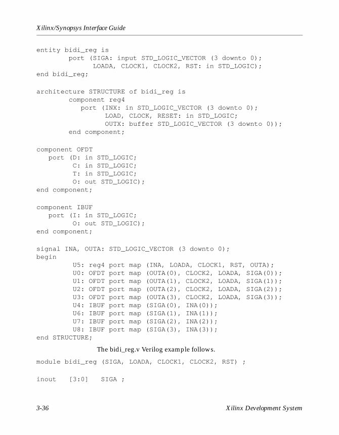
Xilinx/Synopsys Interface Guide
entity bidi_reg is port (SIGA: input STD_LOGIC_VECTOR (3 downto 0); LOADA, CLOCK1, CLOCK2, RST: in STD_LOGIC);end bidi_reg;
architecture STRUCTURE of bidi_reg is component reg4 port (INX: in STD_LOGIC_VECTOR (3 downto 0); LOAD, CLOCK, RESET: in STD_LOGIC; OUTX: buffer STD_LOGIC_VECTOR (3 downto 0)); end component;
component OFDT port (D: in STD_LOGIC; C: in STD_LOGIC; T: in STD_LOGIC; O: out STD_LOGIC);end component;
component IBUF port (I: in STD_LOGIC; O: out STD_LOGIC);end component;
signal INA, OUTA: STD_LOGIC_VECTOR (3 downto 0);begin U5: reg4 port map (INA, LOADA, CLOCK1, RST, OUTA); U0: OFDT port map (OUTA(0), CLOCK2, LOADA, SIGA(0)); U1: OFDT port map (OUTA(1), CLOCK2, LOADA, SIGA(1)); U2: OFDT port map (OUTA(2), CLOCK2, LOADA, SIGA(2)); U3: OFDT port map (OUTA(3), CLOCK2, LOADA, SIGA(3)); U4: IBUF port map (SIGA(0), INA(0)); U6: IBUF port map (SIGA(1), INA(1)); U7: IBUF port map (SIGA(2), INA(2)); U8: IBUF port map (SIGA(3), INA(3));end STRUCTURE;
The bidi_reg.v Verilog example follows.
module bidi_reg (SIGA, LOADA, CLOCK1, CLOCK2, RST) ;
inout [3:0] SIGA ;
3-36 Xilinx Development System
Synthesizing Your Design with FPGA Compiler II
input LOADA ;input CLOCK1 ;input CLOCK2 ;input RST ;
wire [3:0] INA, OUTA ;// Netlist
reg4 U5 (.INPUT(INA), .LD(LOADA), .CLOCK(CLOCK1), .RESET(RST), \
.OUT(OUTA)) ;OFDT U0 (.D(OUTA[0]), .C(CLOCK2), .T(LOADA), .O(SIGA[0])) ;OFDT U1 (.D(OUTA[1]), .C(CLOCK2), .T(LOADA), .O(SIGA[1])) ;OFDT U2 (.D(OUTA[2]), .C(CLOCK2), .T(LOADA), .O(SIGA[2])) ;OFDT U3 (.D(OUTA[3]), .C(CLOCK2), .T(LOADA), .O(SIGA[3])) ;IBUF U4 (.I(SIGA[0]), .O(INA[0])) ;IBUF U6 (.I(SIGA[1]), .O(INA[1])) ;IBUF U7 (.I(SIGA[2]), .O(INA[2])) ;IBUF U8 (.I(SIGA[3]), .O(INA[3])) ;
endmodule
The backslash (“\”) character shows a line break required for formatting purposes.
Implementing 3-State Registered OutputFPGA Compiler II infers the use of 3-state output flip-flops, such as OFDT, under the following two conditions.
• The flip-flop must directly drive the 3-state signal.
• The HDL code of the flip-flop must reside in the same process as the 3-state HDL code.
The following sections illustrate a flip-flop that does not directly drive the 3-state signal and one that does directly drive the 3-state signal.
Example of Not Directly Driving the 3-State SignalIf any logic exists between the flip-flop and the 3-state signal connected to the output flip-flop, FPGA Compiler II does not infer a
Xilinx/Synopsys Interface Guide 3-37
Xilinx/Synopsys Interface Guide
3-state output flip-flop. The following VHDL and Verilog examples illustrate a flip-flop not directly driving a 3-state output flip-flop. Figure 3-19 shows a schematic representation.
The three_ex1 VHDL example follows.
library IEEE;use IEEE.std_logic_1164.all;use IEEE.std_logic_unsigned.all;
entity three_ex1 is port (BUS_IN, EN, CLK: in STD_LOGIC; BUS_OUT: out STD_LOGIC);end three_ex1;
architecture RTL of three_ex1 is
signal BUS_IN_REG, BUS_OUT_REG: STD_LOGIC;
beginsync: process (CLK) begin if (CLK’ event and CLK= ‘1’) then BUS_IN_REG <= BUS_IN; BUS_OUT_REG <= BUS_IN_REG; end if; end process;BUS_OUT <= BUS_OUT_REG when (EN= ‘0’) else ‘Z’;
end RTL;
The three_ex1 Verilog example follows.
module three_ex1(BUS_IN, EN, CLK, BUS_OUT);input BUS_IN ;input EN ;input CLK ;output BUS_OUT ;
reg BUS_OUT_REG, BUS_IN_REG, BUS_OUT;
always @(posedge CLK)begin
3-38 Xilinx Development System
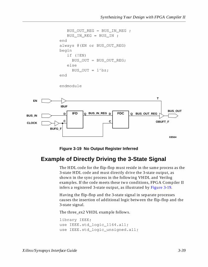
Synthesizing Your Design with FPGA Compiler II
BUS_OUT_REG = BUS_IN_REG ; BUS_IN_REG = BUS_IN ;endalways @(EN or BUS_OUT_REG)begin if (!EN) BUS_OUT = BUS_OUT_REG; else BUS_OUT = 1’bz;end
endmodule
Figure 3-19 No Output Register Inferred
Example of Directly Driving the 3-State SignalThe HDL code for the flip-flop must reside in the same process as the 3-state HDL code and must directly drive the 3-state output, as shown in the sync process in the following VHDL and Verilog examples. If the code meets these two conditions, FPGA Compiler II infers a registered 3-state output, as illustrated by Figure 3-19.
Having the flip-flop and the 3-state signal in separate processes causes the insertion of additional logic between the flip-flop and the 3-state signal.
The three_ex2 VHDL example follows.
library IEEE;use IEEE.std_logic_1164.all;use IEEE.std_logic_unsigned.all;
BUS_OUT
OBUFT_F
BUS_OUT_REGBUS_IN
EN
X8564
DBUS_IN_REG
BUFG_F
IBUF
Q
T
FDC
C
D
C
QIFD
CLOCK
Xilinx/Synopsys Interface Guide 3-39
Xilinx/Synopsys Interface Guide
entity three_ex2 is port (BUS_IN, EN, CLK: in STD_LOGIC; BUS_OUT: out STD_LOGIC);end three_ex2;
architecture RTL of three_ex2 is
signal BUS_IN_REG: STD_LOGIC;
beginsync: process (CLK, EN) begin if (CLK’ event and CLK= ‘1’) then BUS_IN_REG <= BUS_IN; if (EN= ‘0’) then BUS_OUT <= BUS_IN_REG; else BUS_OUT <= ‘Z’; end if; end if; end process;
end RTL;
The three_ex2 Verilog example follows.
module three_ex2(BUS_IN, EN, CLK, BUS_OUT) ;input BUS_IN ;input EN ;input CLK ;output BUS_OUT ;
reg BUS_OUT ;reg BUS_IN_Q, BUS_IN_REG ;
always @(posedge CLK)begin BUS_IN_Q = BUS_IN ; BUS_IN_REG = BUS_IN_Q ; if (!EN) BUS_OUT = BUS_IN_REG; else BUS_OUT = 1’bz;
3-40 Xilinx Development System
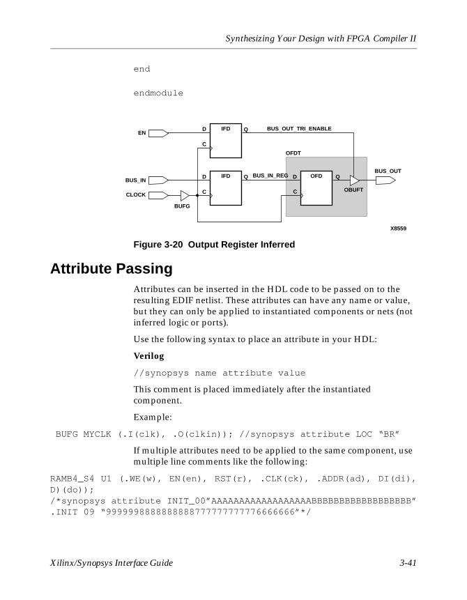
Synthesizing Your Design with FPGA Compiler II
end
endmodule
Figure 3-20 Output Register Inferred
Attribute PassingAttributes can be inserted in the HDL code to be passed on to the resulting EDIF netlist. These attributes can have any name or value, but they can only be applied to instantiated components or nets (not inferred logic or ports).
Use the following syntax to place an attribute in your HDL:
Verilog
//synopsys name attribute value
This comment is placed immediately after the instantiated component.
Example:
BUFG MYCLK (.I(clk), .O(clkin)); //synopsys attribute LOC “BR”
If multiple attributes need to be applied to the same component, use multiple line comments like the following:
RAMB4_S4 U1 (.WE(w), EN(en), RST(r), .CLK(ck), .ADDR(ad), DI(di),D)(do));/*synopsys attribute INIT_00”AAAAAAAAAAAAAAAAAABBBBBBBBBBBBBBBBBB”.INIT 09 “9999998888888888777777777776666666”*/
BUS_OUT
OBUFT
OFDT
BUS_IN
EN
X8559
DBUS_IN_REG
BUS_OUT_TRI_ENABLE
BUFG
QOFD
C
D
C
C
D
QIFD
QIFD
CLOCK
Xilinx/Synopsys Interface Guide 3-41
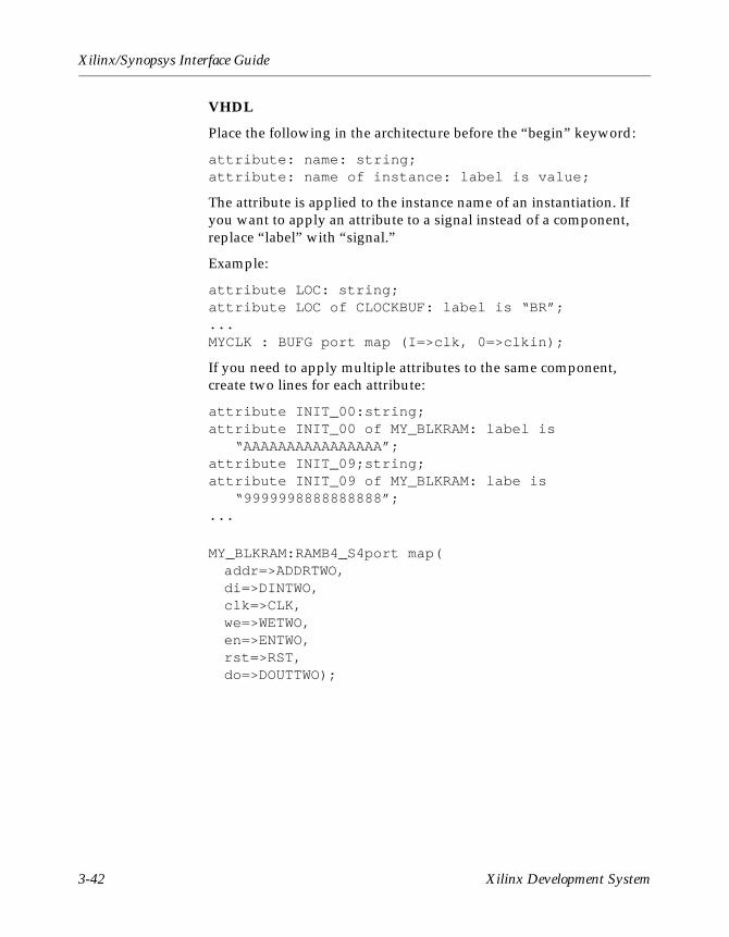
Xilinx/Synopsys Interface Guide
VHDL
Place the following in the architecture before the “begin” keyword:
attribute: name: string;attribute: name of instance: label is value;
The attribute is applied to the instance name of an instantiation. If you want to apply an attribute to a signal instead of a component, replace “label” with “signal.”
Example:
attribute LOC: string;attribute LOC of CLOCKBUF: label is “BR”;...MYCLK : BUFG port map (I=>clk, 0=>clkin);
If you need to apply multiple attributes to the same component, create two lines for each attribute:
attribute INIT_00:string;attribute INIT_00 of MY_BLKRAM: label is
“AAAAAAAAAAAAAAAA”;attribute INIT_09;string;attribute INIT_09 of MY_BLKRAM: labe is
“9999998888888888”;...
MY_BLKRAM:RAMB4_S4port map(addr=>ADDRTWO,di=>DINTWO,clk=>CLK,we=>WETWO,en=>ENTWO,rst=>RST,do=>DOUTTWO);
3-42 Xilinx Development System
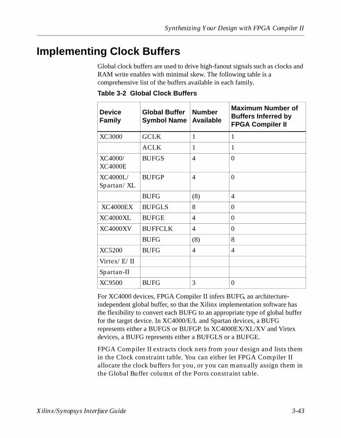
Synthesizing Your Design with FPGA Compiler II
Implementing Clock BuffersGlobal clock buffers are used to drive high-fanout signals such as clocks and RAM write enables with minimal skew. The following table is a comprehensive list of the buffers available in each family.
For XC4000 devices, FPGA Compiler II infers BUFG, an architecture-independent global buffer, so that the Xilinx implementation software has the flexibility to convert each BUFG to an appropriate type of global buffer for the target device. In XC4000/E/L and Spartan devices, a BUFG represents either a BUFGS or BUFGP. In XC4000EX/XL/XV and Virtex devices, a BUFG represents either a BUFGLS or a BUFGE.
FPGA Compiler II extracts clock nets from your design and lists them in the Clock constraint table. You can either let FPGA Compiler II allocate the clock buffers for you, or you can manually assign them in the Global Buffer column of the Ports constraint table.
Table 3-2 Global Clock Buffers
Device Family
Global Buffer Symbol Name
Number Available
Maximum Number of Buffers Inferred by FPGA Compiler II
XC3000 GCLK 1 1
ACLK 1 1
XC4000/XC4000E
BUFGS 4 0
XC4000L/Spartan/XL
BUFGP 4 0
BUFG (8) 4
XC4000EX BUFGLS 8 0
XC4000XL BUFGE 4 0
XC4000XV BUFFCLK 4 0
BUFG (8) 8
XC5200 BUFG 4 4
Virtex/E/II
Spartan-II
XC9500 BUFG 3 0
Xilinx/Synopsys Interface Guide 3-43
Xilinx/Synopsys Interface Guide
When FPGA Compiler II performs the allocation, it uses one BUFG per clock, up to the maximum specified in the last column of the Global Clock Buffers table. Allocation begins with the most heavily-loaded clock signal. For example, if an XC4000E design contains five clock signals, FPGA Compiler II allocates four BUFG buffers to the four most heavily-loaded clocks. Targeting the same design to an XC4000EX device would result in the use of five BUFGs. In XC4000/E/L and Spartan devices, FPGA Compiler II infers a maximum of four global buffers even though eight exist. Inferring more than four buffers could use extra global routing resources, threatening chances of a successful route. XC4000EX/XL/XV and Virtex devices contain extra routing resources so FPGA Compiler II infers up to eight BUFGs (the maximum available in the device) for them.
To perform manual allocation, choose the buffer type in the Global Buffer column of the Ports constraint table. FPGA Compiler II maintains a count of global buffers so that you cannot assign more global buffers than are available for the current device. It is also possible to assign global buffers to non-clock signals.
XC4000EX/XL/XV devices contain BUFGE and BUFFCLK buffers. These buffers are primarily used to implement high-speed I/O interfaces. You can assign these buffers in the Global Buffer column of the Ports constraint table.
For XC9500 devices, FPGA Compiler II does not infer BUFG buffers for clock signals. The Xilinx CPLD implementation tools are responsible for automatically assigning BUFG buffers.
Using MemoryYou can use on-chip RAM for status registers, index registers, counter storage, distributed shift registers, LIFO stacks, and FIFO buffers.
The XC4000 family can efficiently implement RAM and ROM using CLB function generators. Implement a ROM by describing it behaviorally as shown in the Implementing XC4000 ROM section. Alternatively, the XSI XC4000E/L/EX/XL/XV libraries contain 16 x 1 (16 deep x 1 wide) and 32 x 1 (32 deep x 1 wide) RAM and ROM primitives and 16 x 1 dual-port RAM you can instantiate.
3-44 Xilinx Development System
Synthesizing Your Design with FPGA Compiler II
You can also implement memory using the LogiBLOX program. LogiBLOX can create RAM and ROM between 1–32 bits wide and 2–256 bits deep. Using LogiBLOX to add RAM or ROM to your design provides an efficient implementation of your memory in addition to a simulation model for Register Transfer Level (RTL) simulation.
For VHDL and Verilog examples of instantiating RAM in your designs using CoreGen or LogiBLOX, refer to the “Using CORE Generator and LogiBLOX” chapter. Also, refer to the LogiBLOX Guide for more information on LogiBLOX.
Implementing Virtex/E/-II RAMImplement RAMs in your HDL with the following methods.
• Instantiate 16 x 1 and 32 x 1 distributed RAM from the Unified primitive libraries.
• Instantiate Block RAM components from the Unified primitive libraries.
• Instantiate any size Block RAM using CoreGen.
The INIT values for RAM32X 1 and RAM32X1_1 map differently from 4000EX/XL/XV and Spartan/XL.
Virtex maps the lower INIT values to G and upper INIT values to F for both RAM32X. 4000EX/XL/XV and SpartanXL map those lower INIT values to F and upper INIT values to G.
Behaviorally describing RAMs in VHDL creates combinatorial loops during compiling.
Implementing XC4000 RAMImplement RAMs in your HDL with the following methods.
• Instantiate 16 x 1 and 32 x 1 RAMs from the XSI primitive libraries.
• Instantiate any size RAM using LogiBLOX.
Behaviorally describing RAMs in VHDL creates combinatorial loops during compiling.
Xilinx/Synopsys Interface Guide 3-45
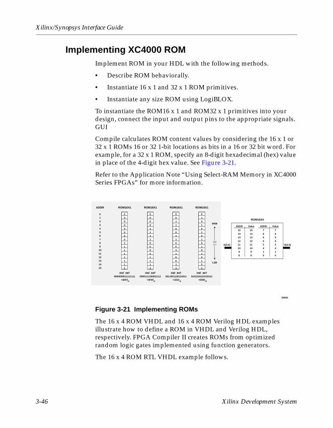
Xilinx/Synopsys Interface Guide
Implementing XC4000 ROMImplement ROM in your HDL with the following methods.
• Describe ROM behaviorally.
• Instantiate 16 x 1 and 32 x 1 ROM primitives.
• Instantiate any size ROM using LogiBLOX.
To instantiate the ROM16 x 1 and ROM32 x 1 primitives into your design, connect the input and output pins to the appropriate signals. GUI
Compile calculates ROM content values by considering the 16 x 1 or 32 x 1 ROMs 16 or 32 1-bit locations as bits in a 16 or 32 bit word. For example, for a 32 x 1 ROM, specify an 8-digit hexadecimal (hex) value in place of the 4-digit hex value. See Figure 3-21.
Refer to the Application Note “Using Select-RAM Memory in XC4000 Series FPGAs” for more information.
Figure 3-21 Implementing ROMs
The 16 x 4 ROM VHDL and 16 x 4 ROM Verilog HDL examples illustrate how to define a ROM in VHDL and Verilog HDL, respectively. FPGA Compiler II creates ROMs from optimized random logic gates implemented using function generators.
The 16 x 4 ROM RTL VHDL example follows.
0
1
2
3
4
5
6
7
8
9
10
11
12
13
14
15
ADDR
0
0
0
0
0
0
0
0
1
1
1
1
1
1
1
1
ROM16X1
XNF_INIT0000000011111111
=00FFH
0
0
0
0
1
1
1
1
0
0
0
0
1
1
1
1
ROM16X1
XNF_INIT0000111100001111
=0F0FH
0
0
1
1
0
0
1
1
0
0
1
1
0
0
1
1
ROM16X1
XNF_INIT0011001100110011
=3333H
0
1
0
1
0
1
0
1
0
1
0
1
0
1
0
1
ROM16X1
XNF_INIT0101010101010101
=5555H
MSB
LSB
15
14
13
12
11
10
9
8
ADDR
15
14
13
12
11
10
9
8
Value
7
6
5
4
3
2
1
0
ADDR
7
6
5
4
3
2
1
0
Value
A[3:0] O[3:0]
ROM16X4
X8001
3-46 Xilinx Development System
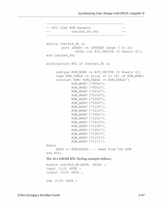
Synthesizing Your Design with FPGA Compiler II
------------------------------------------- RTL 16x4 ROM Example ---- rom16x4_4k.vhd -------------------------------------------
entity rom16x4_4k is port (ADDR: in INTEGER range 0 to 15; DATA: out BIT_VECTOR (3 downto 0));end rom16x4_4k;
architecture RTL of rom16x4_4k is
subtype ROM_WORD is BIT_VECTOR (3 downto 0); type ROM_TABLE is array (0 to 15) of ROM_WORD; constant ROM: ROM_TABLE := ROM_TABLE’( ROM_WORD’(“0000”), ROM_WORD’(“0001”), ROM_WORD’(“0010”), ROM_WORD’(“0100”), ROM_WORD’(“1000”), ROM_WORD’(“1000”), ROM_WORD’(“1100”), ROM_WORD’(“1010”), ROM_WORD’(“1001”), ROM_WORD’(“1001”), ROM_WORD’(“1010”), ROM_WORD’(“1100”), ROM_WORD’(“1001”), ROM_WORD’(“1001”), ROM_WORD’(“1101”), ROM_WORD’(“1111”),begin DATA <= ROM(ADDR); -- Read from the ROMend RTL;
The 16 x 4 ROM RTL Verilog example follows.
module rom16x4_4k(ADDR, DATA) ;input [3:0] ADDR ;output [3:0] DATA ;
reg [3:0] DATA ;
Xilinx/Synopsys Interface Guide 3-47
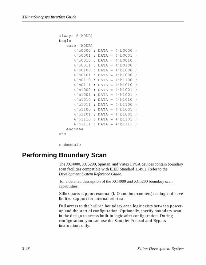
Xilinx/Synopsys Interface Guide
always @(ADDR)begin case (ADDR) 4’b0000 : DATA = 4’b0000 ; 4’b0001 : DATA = 4’b0001 ; 4’b0010 : DATA = 4’b0010 ; 4’b0011 : DATA = 4’b0100 ; 4’b0100 : DATA = 4’b1000 ; 4’b0101 : DATA = 4’b1000 ; 4’b0110 : DATA = 4’b1100 ; 4’b0111 : DATA = 4’b1010 ; 4’b1000 : DATA = 4’b1001 ; 4’b1001 : DATA = 4’b1001 ; 4’b1010 : DATA = 4’b1010 ; 4’b1011 : DATA = 4’b1100 ; 4’b1100 : DATA = 4’b1001 ; 4’b1101 : DATA = 4’b1001 ; 4’b1110 : DATA = 4’b1101 ; 4’b1111 : DATA = 4’b1111 ; endcaseend
endmodule
Performing Boundary ScanThe XC4000, XC5200, Spartan, and Virtex FPGA devices contain boundary scan facilities compatible with IEEE Standard 1149.1. Refer to the Development System Reference Guide.
for a detailed description of the XC4000 and XC5200 boundary scan capabilities.
Xilinx parts support external (I/O and interconnect) testing and have limited support for internal self-test.
Full access to the built-in boundary-scan logic exists between power-up and the start of configuration. Optionally, specify boundary scan in the design to access built-in logic after configuration. During configuration, you can use the Sample/Preload and Bypass instructions only.
3-48 Xilinx Development System
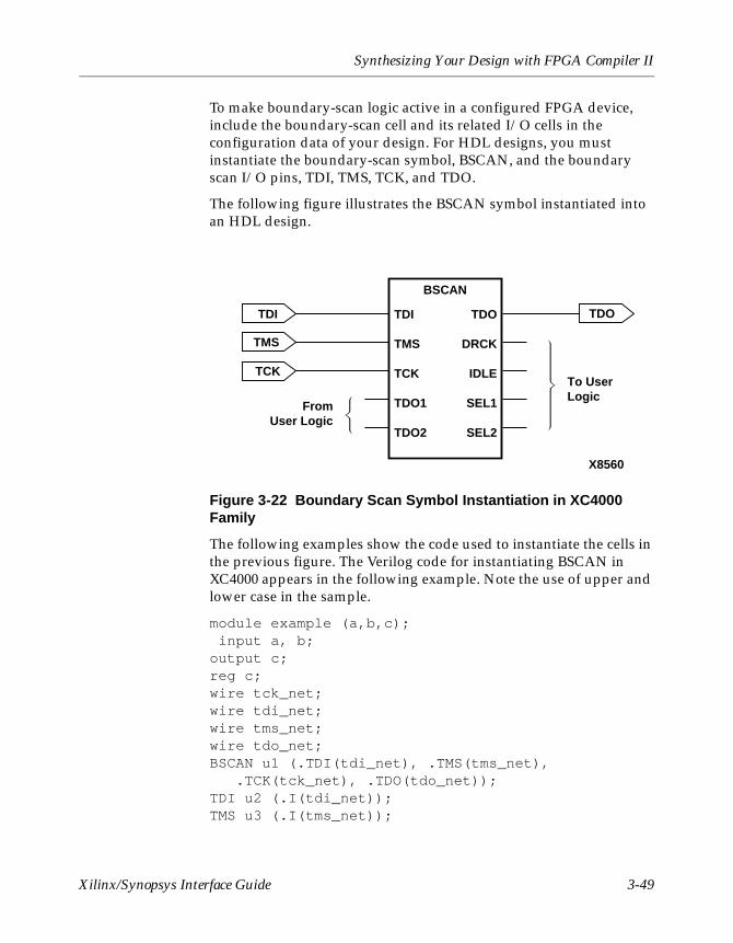
Synthesizing Your Design with FPGA Compiler II
To make boundary-scan logic active in a configured FPGA device, include the boundary-scan cell and its related I/O cells in the configuration data of your design. For HDL designs, you must instantiate the boundary-scan symbol, BSCAN, and the boundary scan I/O pins, TDI, TMS, TCK, and TDO.
The following figure illustrates the BSCAN symbol instantiated into an HDL design.
Figure 3-22 Boundary Scan Symbol Instantiation in XC4000 Family
The following examples show the code used to instantiate the cells in the previous figure. The Verilog code for instantiating BSCAN in XC4000 appears in the following example. Note the use of upper and lower case in the sample.
module example (a,b,c); input a, b;output c;reg c;wire tck_net;wire tdi_net;wire tms_net;wire tdo_net;BSCAN u1 (.TDI(tdi_net), .TMS(tms_net),
.TCK(tck_net), .TDO(tdo_net));TDI u2 (.I(tdi_net));TMS u3 (.I(tms_net));
TDI
TMS
TCK
TDO1
TDO2
TDO
DRCK
IDLE
SEL1
SEL2
TDI
TMS
TCK
TDO
BSCAN
FromUser Logic
To UserLogic
X8560
Xilinx/Synopsys Interface Guide 3-49
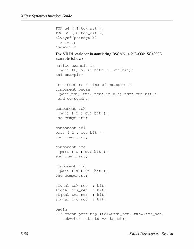
Xilinx/Synopsys Interface Guide
TCK u4 (.I(tck_net));TDO u5 (.O(tdo_net));always@(posedge b)c <= a;
endmodule
The VHDL code for instantiating BSCAN in XC4000/XC4000E example follows.
entity example isport (a, b: in bit; c: out bit);
end example;
architecture xilinx of example iscomponent bscanport(tdi, tms, tck: in bit; tdo: out bit);
end component;
component tckport ( i : out bit );
end component;
component tdiport ( i : out bit );end component;
component tmsport ( i : out bit );
end component;
component tdoport ( o : in bit );
end component;
signal tck_net : bit;signal tdi_net : bit;signal tms_net : bit;signal tdo_net : bit;
beginu1: bscan port map (tdi=>tdi_net, tms=>tms_net,
tck=>tck_net, tdo=>tdo_net);
3-50 Xilinx Development System
Synthesizing Your Design with FPGA Compiler II
u2: tck port map (i=>tck_net);u3: tdi port map (i=>tdi_net);u4: tms port map (i=>tms_net);u5: tdo port map (o=>tdo_net);
process(b)beginif(b’event and b=’1’) then c <= a;end if;end process;
end xilinx;
The Verilog code for instantiating BSCAN in XC4000/XC4000E appears in the following example. Note the use of upper and lower case in the sample.
module example (a,b,c);input a, b;output c;reg c;wire tck_net;wire tdi_net;wire tms_net;wire tdo_net;BSCAN u1 (.TDI(tdi_net), .TMS(tms_net),
.TCK(tck_net), .TDO(tdo_net));TDI u2 (.I(tdi_net));TMS u3 (.I(tms_net));TCK u4 (.I(tck_net));TDO u5 (.O(tdo_net));always@(posedge b) c<=a;endmodule
The VHDL code for instantiating BSCAN in XC4000/XC4000E example follows.
entity example is port (a, b: in bit; c: out bit);end example;
Xilinx/Synopsys Interface Guide 3-51
Xilinx/Synopsys Interface Guide
architecture xilinx of example iscomponent bscan port(tdi, tms, tck: in bit; tdo: out bit);end component;
component tck port ( i : out bit );end component;
component tdi port ( i : out bit );end component;
component tms port ( i : out bit );end component;
component tdo port ( o : in bit );end component;
signal tck_net : bit;signal tdi_net : bit;signal tms_net : bit;signal tdo_net : bit;
beginu1: bscan port map (tdi=>tdi_net, tms=>tms_net,
tck=>tck_net, tdo=>tdo_net);u2: tck port map (i=>tck_net);u3: tdi port map (i=>tdi_net);u4: tms port map (i=>tms_net);u5: tdo port map (o=>tdo_net);
process(b)beginif(b’event and b=’1’) then c <= a;end if;end process;end xilinx;
3-52 Xilinx Development System
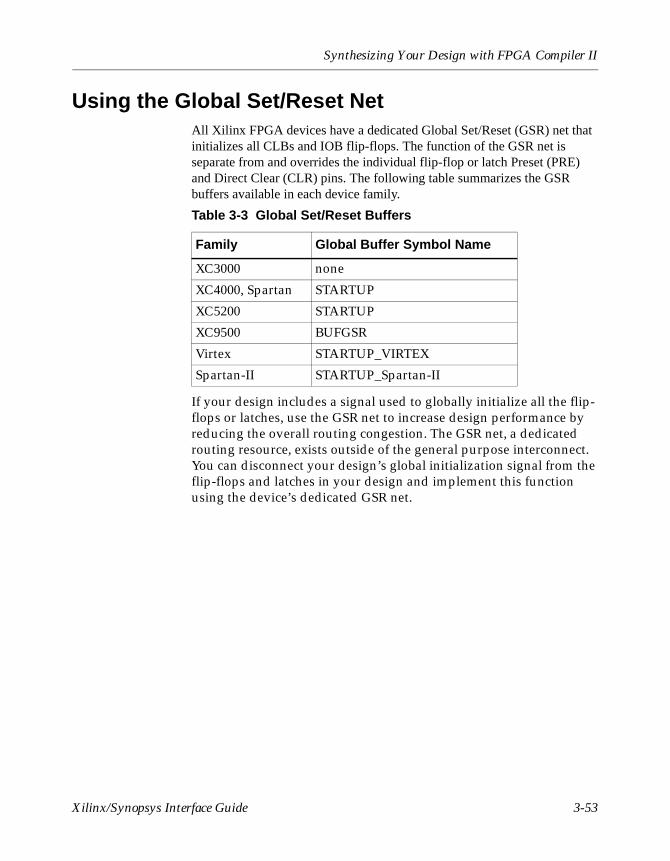
Synthesizing Your Design with FPGA Compiler II
Using the Global Set/Reset NetAll Xilinx FPGA devices have a dedicated Global Set/Reset (GSR) net that initializes all CLBs and IOB flip-flops. The function of the GSR net is separate from and overrides the individual flip-flop or latch Preset (PRE) and Direct Clear (CLR) pins. The following table summarizes the GSR buffers available in each device family.
If your design includes a signal used to globally initialize all the flip-flops or latches, use the GSR net to increase design performance by reducing the overall routing congestion. The GSR net, a dedicated routing resource, exists outside of the general purpose interconnect. You can disconnect your design’s global initialization signal from the flip-flops and latches in your design and implement this function using the device’s dedicated GSR net.
Table 3-3 Global Set/Reset Buffers
Family Global Buffer Symbol Name
XC3000 none
XC4000, Spartan STARTUP
XC5200 STARTUP
XC9500 BUFGSR
Virtex STARTUP_VIRTEX
Spartan-II STARTUP_Spartan-II
Xilinx/Synopsys Interface Guide 3-53
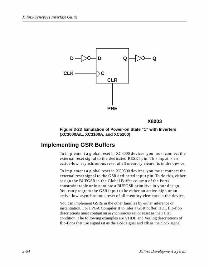
Xilinx/Synopsys Interface Guide
Figure 3-23 Emulation of Power-on State “1” with Inverters (XC3000A/L, XC3100A, and XC5200)
Implementing GSR BuffersTo implement a global reset in XC3000 devices, you must connect the external reset signal to the dedicated RESET pin. This input is an active-low, asynchronous reset of all memory elements in the device.
To implement a global reset in XC9500 devices, you must connect the external reset signal to the GSR dedicated input pin. To do this, either assign the BUFGSR in the Global Buffer column of the Ports constraint table or instantiate a BUFGSR primitive in your design. You can program the GSR input to be either an active-high or an active-low asynchronous reset of all memory elements in the device.
You can implement GSRs in the other families by either inference or instantiation. For FPGA Compiler II to infer a GSR buffer, HDL flip-flop descriptions must contain an asynchronous set or reset as their first condition. The following examples are VHDL and Verilog descriptions of flip-flops that use signal rst as the GSR signal and clk as the clock signal.
CLK
QD
CLR
PRE
QD
C
X8003
3-54 Xilinx Development System
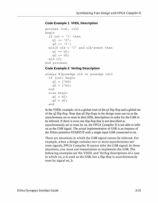
Synthesizing Your Design with FPGA Compiler II
Code Example 1 VHDL Description
process (rst, clk)beginif rst = ‘1’ then
q1 <= ‘0’;q2 <= ‘1’;
elsif clk = ‘1’ and clk’event thenq1 <= d1;q2 <= d2;
end if;end process;
Code Example 2 Verilog Description
always @(posedge clk or posedge rst)if (rst) begin
q1 = 1’b0;q2 = 1’b1;
endelse begin
q1 = d1;q2 = d2;
end
In the VHDL example, rst is a global reset of the q1 flip-flop and a global set of the q2 flip-flop. Note that all flip-flops in the design must use rst as the asynchronous set or reset in their HDL descriptions in order for the GSR to be inferred. If there is even one flip-flop that is not described as asynchronously set or reset by rst, the FPGA Compiler II is not able to infer rst as the GSR signal. The actual implementation of GSR is an instance of the Xilinx primitive STARTUP with a single input GSR connected to rst.
There are situations in which the GSR signal cannot be inferred. For example, when a design contains two or more asynchronous set/reset signals, FPGA Compiler II cannot infer the GSR signal. In these situations, you must use instantiation to implement the GSR. The following examples are the VHDL and Verilog descriptions of a case in which rst_a is used as the GSR, but a flip-flop is asynchronously reset by signal rst_b.
Xilinx/Synopsys Interface Guide 3-55
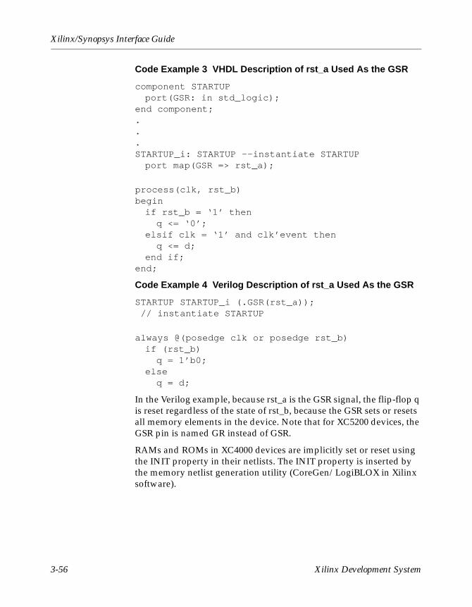
Xilinx/Synopsys Interface Guide
Code Example 3 VHDL Description of rst_a Used As the GSR
component STARTUPport(GSR: in std_logic);
end component;...STARTUP_i: STARTUP --instantiate STARTUPport map(GSR => rst_a);
process(clk, rst_b)beginif rst_b = ‘1’ then
q <= ‘0’;elsif clk = ‘1’ and clk’event then
q <= d;end if;
end;
Code Example 4 Verilog Description of rst_a Used As the GSR
STARTUP STARTUP_i (.GSR(rst_a)); // instantiate STARTUP
always @(posedge clk or posedge rst_b)if (rst_b)
q = 1’b0;else
q = d;
In the Verilog example, because rst_a is the GSR signal, the flip-flop q is reset regardless of the state of rst_b, because the GSR sets or resets all memory elements in the device. Note that for XC5200 devices, the GSR pin is named GR instead of GSR.
RAMs and ROMs in XC4000 devices are implicitly set or reset using the INIT property in their netlists. The INIT property is inserted by the memory netlist generation utility (CoreGen/LogiBLOX in Xilinx software).
3-56 Xilinx Development System
Synthesizing Your Design with FPGA Compiler II
If a design contains a black box, such as a netlist from CoreGen or LogiBLOX, FPGA Compiler II can still infer the GSR as long as all flip-flops in the design are asynchronously set or reset by the same signal. In this case, you must select the “Infer GSR if design contains unlinked cells” option in the Xilinx Options page of the constraint tables.
Accessing Global Set/Reset Using STARTBUFAccess an FPGA’s GSR signal by attaching a net to the input pin on the STARTBUF cell. Asserting the net attached to the STARTBUF block’s GSR pin also asserts FPGA Global Set/Reset causing every flip-flop and latch in the device to assume its power-on state.
You must instantiate the STARTBUF block.
The GSR net does not appear in the pre-placed and routed netlist. Asserting the GSR signal to High (the default) sets every flip-flop and latch to the same state it had at the end of configuration, illustrated in the following tables. When you simulate the placed and routed design, the simulator’s translation program correctly inserts the functionality.
Any signal can drive the STARTUP block’s GSR pin, however, do not use flip-flop or latch output signals.
Synthesizing/Simulating for VHDL Global Set/Reset Emulation
VHDL requires a testbench to control all signal ports. You can instantiate certain VHDL-specific components, explained in the following sections, in the RTL and post-synthesis VHDL description to allow the simulation of the global signals for global set/reset and global 3-state.
NGD2VHDL creates a port in your back-annotated design entity for stimulating the global set/reset or 3-state enable signals. This port does not actually exist on the configured part.
Xilinx/Synopsys Interface Guide 3-57
Xilinx/Synopsys Interface Guide
Using STARTBUF in VHDL
STARTBUF replaces STARTUP. With STARTBUF you can functionally simulate the GSR/GR net in both function and timing simulation. By connecting the input pin of the STARTBUF to a top-level port and using STARTBUF as the source for all asynchronous set/reset signals in a design, Xilinx software can automatically optimize the design to use the GSR/GR. Because you can use STARTBUF in functional simulation (unlike STARTUP), when you use STARTBUF you can map to the GSR/GR in a device. You can still use STARTUP, but it does not always provide correct GSR/GR in HDL flows.
The STARTBUF component passes a reset or 3-state signal in the same way that a buffer allows simulation to proceed and also instantiates the STARTUP block for implementation. One version of STARTBUF works for all devices, however, the XC5200 and the XC4000 STARTUP blocks have different pin names. Implementation with the correct STARTUP block occurs automatically. The following shows an instantiation example of the STARTBUF component.
U1: STARTBUF port map (GSRIN => DEV_GSR_PORT, GTSIN =>DEV_GTS_PORT, CLKIN => ‘0’, GSROUT => GSR_NET, GTSOUT => GTS_NET, Q2OUT => open, Q3OUT => open, Q1Q4OUT => open, DONEINOUT => open):
You can use one or both of the input ports (GSRIN and GTSIN) of the STARTBUF component and the associated output ports (GSROUT and GTSOUT). You can use pins left open to pass configuration instructions to the implementation tools by connecting the appropriate signal to the port instead of leaving it open.
Instantiating a STARTUP Block in VHDL
The STARTUP block traditionally instantiates to identify the GR, PRLD, or GSR signals for implementation. However, simulation can occur only when the net attached to the GSR or GTS goes off the chip because the STARTUP block does not have a simulation model. You can use the new components described below to simulate global set/reset or 3-state nets whether or not the signal goes off the chip.
3-58 Xilinx Development System
Synthesizing Your Design with FPGA Compiler II
Setting Direct Preset or Direct ClearYou can program each flip-flop and latch as either Preset or Clear but not both. The device’s automatic assertion of its own GSR net asynchronously sets flip-flops and latches as either Preset or Cleared upon completion of configuration. Use individual flip-flop and latch Preset (PRE) and Clear (CLR) pins to set them as preset or cleared.
The power-on state of a register or latch and the selection of PRE or CLR pin must match. For example, a register with a CLR pin assumes the value of 0 on power-up. Alternatively, a register with a power-up state of 0 can only have a CLR pin.
To get an asynchronous set or asynchronous reset flip-flop, describe the behavior in the RTL code. If you only want to describe the power-on state of a flip-flop, connect the asynchronous set or asynchronous reset signal of the RTL flip-flop to the ROCBUF.
Increasing Performance with the GSR NetMany designs have a net that initializes the majority of the design’s flip-flops. If this signal initializes all the design’s flip-flops, you can use the GSR net.
To have your HDL simulation match that of the resulting design, modify your HDL code so that asserting the GSR signal presets or clears every flip-flop and latch. FPGA Compiler II only routes this signal to the dedicated STARTUP component, using the dedicated global routing resource, so this signal does not get routed with general purpose interconnect.
Alternatively, the Xilinx tools move this signal on to the device’s dedicated GSR routing network when the following conditions apply.
• The asynchronous Preset or Clear pin of every register in your design that has this pin connects to the same net.
• That net connects to the GSR pin of the STARTUP block.
• You use STARTBUF (see the “Using the Xilinx Development System” section).
The following figure illustrates this flow.
Xilinx/Synopsys Interface Guide 3-59
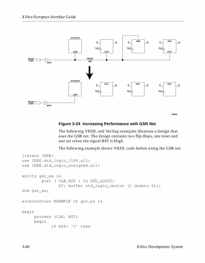
Xilinx/Synopsys Interface Guide
Figure 3-24 Increasing Performance with GSR Net
The following VHDL and Verilog examples illustrate a design that uses the GSR net. The design contains two flip-flops, one reset and one set when the signal RST is High.
The following example shows VHDL code before using the GSR net.
library IEEE;use IEEE.std_logic_1164.all;use IEEE.std_logic_unsigned.all;
entity gsr_ex is port ( CLK,RST : in STD_LOGIC; ST: buffer std_logic_vector (1 downto 0));end gsr_ex;
architecture EXAMPLE of gsr_ex is
begin process (CLK, RST) begin if RST= ‘1’ then
CLK
QD
CLK
QD
CLK
QD
IBUF
CLK
CLR CLR
QD
CLK
QD QD FDC
FDC FDP FDC
PRE
IBUFPORTRESET
PORTRESET
RESETNET
STARTUP
GSR
CLK
STARTUP
GSR
X8002
3-60 Xilinx Development System
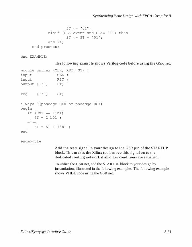
Synthesizing Your Design with FPGA Compiler II
ST <= “01”; elsif (CLK’event and CLK= ‘1’) then ST <= ST + “01”; end if; end process;
end EXAMPLE;
The following example shows Verilog code before using the GSR net.
module gsr_ex (CLK, RST, ST) ;input CLK ;input RST ;output [1:0] ST;
reg [1:0] ST;
always @(posedge CLK or posedge RST)begin if (RST == 1’b1) ST = 2’b01 ; else ST = ST + 1’b1 ;end
endmodule
Add the reset signal in your design to the GSR pin of the STARTUP block. This makes the Xilinx tools move this signal on to the dedicated routing network if all other conditions are satisfied.
To utilize the GSR net, add the STARTUP block to your design by instantiation, illustrated in the following examples. The following example shows VHDL code using the GSR net.
Xilinx/Synopsys Interface Guide 3-61
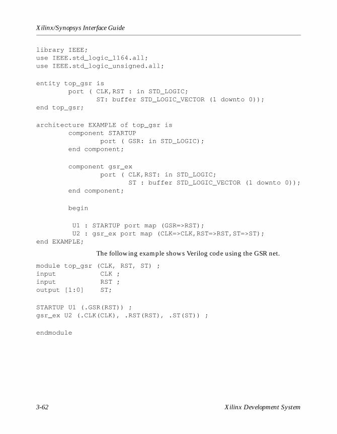
Xilinx/Synopsys Interface Guide
library IEEE;use IEEE.std_logic_1164.all;use IEEE.std_logic_unsigned.all;
entity top_gsr is port ( CLK,RST : in STD_LOGIC; ST: buffer STD_LOGIC_VECTOR (1 downto 0));end top_gsr;
architecture EXAMPLE of top_gsr is component STARTUP port ( GSR: in STD_LOGIC); end component;
component gsr_ex port ( CLK,RST: in STD_LOGIC; ST : buffer STD_LOGIC_VECTOR (1 downto 0)); end component;
begin
U1 : STARTUP port map (GSR=>RST); U2 : gsr_ex port map (CLK=>CLK,RST=>RST,ST=>ST);end EXAMPLE;
The following example shows Verilog code using the GSR net.
module top_gsr (CLK, RST, ST) ;input CLK ;input RST ;output [1:0] ST;
STARTUP U1 (.GSR(RST)) ;gsr_ex U2 (.CLK(CLK), .RST(RST), .ST(ST)) ;
endmodule
3-62 Xilinx Development System
Chapter 4
Synthesizing Your Design with FPGA Compiler and Design Compiler
Synthesize and implement your HDL designs for Xilinx FPGA devices with either FPGA Compiler or Design Compiler by using the information in the following sections.
• “Before You Begin”
• “Naming Conventions”
• “Setting the Wire-Load Model”
• “Setting the Operating Condition Parameters”
• “Configuring IOBs”
• “Inserting Clock Buffers”
• “Using Memory”
• “Performing Boundary Scan”
• “Using the Global Set/Reset Net”
• “Using the Xilinx DesignWare Library”
• “Creating the Area Report”
• “Compiling Your Design”
• “Creating the Area Report”
• “Evaluating Timing Delays”
• “Generating Reports for Debugging”
• “Writing and Saving Your Design”
• “Using the Xilinx Development System”
Xilinx/Synopsys Interface Guide 4-1
Xilinx/Synopsys Interface Guide
Before You BeginBefore you begin a Xilinx design using the Synopsys tools, read the “Getting Started” chapter and ensure the following.
• Verify the installation of Xilinx software on your system.
• Modify the Xilinx-provided default Synopsys startup file, if applicable.
• Verify that you use Synopsys version 1999.05 or later for FPGA Compiler and Design Compiler.
Xilinx does not support the following library cells in the Spartan design flow because they do not exist in the Spartan architecture.
• RAM16X1
• RAM32X1
• DECODEx
• WANDx
• WOR2AND
• MD0
• MD1
• MD2
Naming ConventionsUnless otherwise noted, the following naming conventions are used to group Xilinx device families:
• Virtex represents Virtex, Virtex-E, Virtex-II and Spartan-II devices.
• Spartan represents Spartan and SpartanXL devices.
• XC4000 represents XC4000E, XC4000L, XC4000EX, XC4000XL, XC4000XLA and XC4000XV devices.
• XC9500 represents XC9500, XC9500XL, XC9500XV and XC9500XVA devices.
• XC3000 represents XC3100 and XC3100A devices.
• XC5200 represents XC5200 devices.
4-2 Xilinx Development System
Synthesizing Your Design with FPGA Compiler
Setting the Wire-Load ModelEach primitive library contains device and speed-grade specific estimated pre-layout and routing wire-load models. The Synopsys tools can use these estimates when optimizing your design for an FPGA. XSI provides two wire-load models per device-speed grade combination, an average model and a worst-case model. These models receive “_avg” and “_wc” designations, respectively; the default is average. Using the default (average) wire loads produces more realistic designs.
To change a wire load model, use the following syntax.
set_wire_load “parttype –s.wc”
Substitute the part type to change for parttype.
Run synlibs with the –h option to get a listing of all available part type and speed grade combinations. You can also refer to the Xilinx online Data Book at http://www.xilinx.com/support for current speed grade information.
Setting the Operating Condition ParametersYou need only one set of operating condition parameters, the worst-case commercial (WCCOM) parameter. This set of parameters is the default in the Xilinx libraries.
Configuring IOBsThis section describes how to configure FPGA IOBs. You must implement some features manually, but FPGA Compiler performs the following optimization functions automatically.
• Inserts input buffers (IBUF) and output buffers (OBUF)
• Inserts IBUFs and 3-state output buffers (OBUFT) for bidirectional I/O (IOBUF)
• Inserts a clock buffer for ports driving clock pins (BUFG)
Note: The following functions apply only to FPGAs with I/O flip-flops.
Xilinx/Synopsys Interface Guide 4-3
Xilinx/Synopsys Interface Guide
• Optimizes a flip-flop (IFD) without a clock enable, or latch (ILD_1) attached to input buffers into the IOB
• Optimizes a flip-flop without a clock enable attached to output buffers into the IOB (OFD)
Indicate which ports in your design to use for chip-level I/Os with the Set Port Is Pad command. The Insert Pads command adds the correct buffers to the ports declared as pads, as shown in the following example.
set_port_is_pad “*”
insert_pads
All ArchitecturesThis section includes general information about IOBs that applies to all supported device architectures.
Optimizing Inputs
FPGA Compiler optimizes any flip-flops connected to an input port into the IOB if the flip-flop or latch does not use the Clock Enable, Direct Clear, or Preset pin.
You can configure the buffered input signal that drives the data input of a storage element as either a flip-flop or a latch. You can use the buffered signal in conjunction with the input flip-flop or latch.
A delay buffer added to the signal feeding the data input of the input flip-flop/latch avoids a possible hold time violation. Instantiating a flip-flop or latch, such as an IFD_F or ILD_1F, removes this delay because these cells include a NODELAY attribute. Refer to the “XSI Library Primitives” appendix for a complete list of primitives that include NODELAY attributes.
Understanding and Using Slew Rate
The output buffers have a default slow slew rate that alleviates ground-bounce problems and the option of a fast slew rate that reduces the output delay. The SLOW option increases the transition time and reduces the noise level. The FAST option decreases the transition time and increases the noise level.
4-4 Xilinx Development System
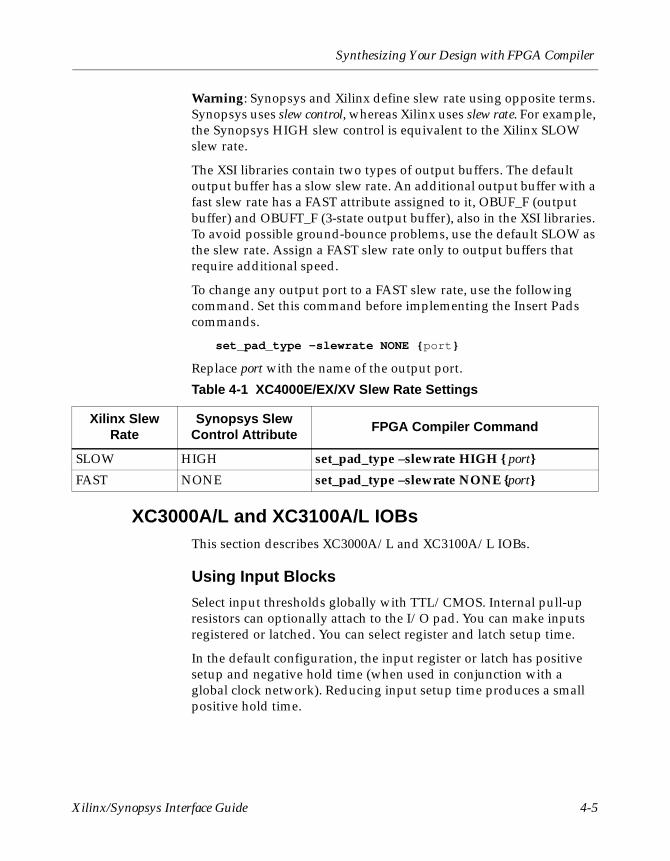
Synthesizing Your Design with FPGA Compiler
Warning: Synopsys and Xilinx define slew rate using opposite terms. Synopsys uses slew control, whereas Xilinx uses slew rate. For example, the Synopsys HIGH slew control is equivalent to the Xilinx SLOW slew rate.
The XSI libraries contain two types of output buffers. The default output buffer has a slow slew rate. An additional output buffer with a fast slew rate has a FAST attribute assigned to it, OBUF_F (output buffer) and OBUFT_F (3-state output buffer), also in the XSI libraries. To avoid possible ground-bounce problems, use the default SLOW as the slew rate. Assign a FAST slew rate only to output buffers that require additional speed.
To change any output port to a FAST slew rate, use the following command. Set this command before implementing the Insert Pads commands.
set_pad_type –slewrate NONE {port}
Replace port with the name of the output port.
XC3000A/L and XC3100A/L IOBsThis section describes XC3000A/L and XC3100A/L IOBs.
Using Input Blocks
Select input thresholds globally with TTL/CMOS. Internal pull-up resistors can optionally attach to the I/O pad. You can make inputs registered or latched. You can select register and latch setup time.
In the default configuration, the input register or latch has positive setup and negative hold time (when used in conjunction with a global clock network). Reducing input setup time produces a small positive hold time.
Table 4-1 XC4000E/EX/XV Slew Rate Settings
Xilinx Slew Rate
Synopsys Slew Control Attribute
FPGA Compiler Command
SLOW HIGH set_pad_type –slewrate HIGH { port}
FAST NONE set_pad_type –slewrate NONE {port}
Xilinx/Synopsys Interface Guide 4-5
Xilinx/Synopsys Interface Guide
Registered and latched inputs become available simultaneously with direct input. You have no clock or latch-enable or asynchronous set/reset control on input registers and latches, but you can control the initial state of input registers and latches.
Using Output Blocks
You can select the output driver slew rate. The output driver by default uses a slow slew rate setting to reduce system noise and power. A faster slew rate decreases chip-to-out propagation delay.
You can register outputs and make them tristate.
You cannot apply clock-enable or asynchronous set/reset control on output registers, but you can control the initial state of output registers.
Using Bidirectional Mode
You cannot use internal pull-up resistors in this mode.
You can select the output driver slew rate. The output driver by default uses a slow slew rate setting to reduce system noise and power. A faster slew rate decreases chip-to-out propagation delay.
Select input thresholds globally with TTL/CMOS. Input can be registered or latched, and you can select register and latch setup time.
In the default configuration, the input register or latch has positive setup and negative hold time (when used in conjunction with a global clock network). Reducing input setup time slightly increases hold time.
You cannot apply clock or latch-enable or asynchronous set/reset control on input registers and latches. Direct input enables simultaneous availability of registered and latched input.
You can control the initial state of input registers and latches, and you can register output.
You cannot apply clock-enable or asynchronous set/reset control on output registers, but you can control the initial state of output registers.
4-6 Xilinx Development System
Synthesizing Your Design with FPGA Compiler
XC4000 IOBsThis section describes XC4000 IOBs.
Using Input Blocks
Select input thresholds globally with TTL/CMOS. Specify an internal pull-up/pull-down resistor that can optionally attach to an I/O pad.
You can make inputs registered or latched, and you can select register and latch setup time.
In the default configuration, the input register or latch has positive setup and zero hold time (when used in conjunction with a global clock network). For XC4000 devices, reducing input setup time slightly increases hold time. For XC4000EX/XL/XLA/XV devices, three setup and hold delay adjustments allow setup versus hold parameter tuning.
Direct input enables simultaneous availability of registered and latched input. You cannot apply asynchronous set/reset control on input registers and latches, but you can apply clocks and latches on input register and latches.
FPGA Compiler cannot infer I/O registers and latches with clock and latch-enables.
You can control the initial state of input registers and latches.
Using Output Blocks
You can select the output driver slew rate. By default, the output driver uses a slow slew rate setting to reduce system noise and power. A faster slew rate decreases chip-to-out propagation delay.
You can register outputs and make them tristate. You cannot enable asynchronous set/reset control on output registers, but you can specify clock-enable on output registers. FPGA Compiler cannot infer I/O registers and latches with clock and latch enables.
You can control the initial state of output registers.
Perform 2-to-1 multiplexing or 2-input function directly in the output path of an IOB (XC4000EX/XL/XV only). You can trade an output register for a 2-input function or multiplexer. Additionally, you must instantiate the following primitives (valid for XC4000EX/XL/XLA/
Xilinx/Synopsys Interface Guide 4-7
Xilinx/Synopsys Interface Guide
XV/XLT). See the “XSI Library Primitives” appendix for more details.
• OAND2
• OMUX2
• ONAND2
• ONOR2
• OOR2
• OXNOR2
• OXOR2
FPGA Compiler cannot infer output drivers containing a 2-input function or output multiplexer.
Using Bidirectional Mode
You can select the output driver slew rate. By default the output driver uses a slow slew rate setting to reduce system noise and power. Faster slew rates decrease chip-to-out propagation delay.
Select input thresholds globally with TTL/CMOS. Input can be registered or latched, and you can select register and latch setup time.
In the default configuration, the input register or latch has positive setup and negative hold time (when used in conjunction with a global clock network). This corresponds to a full delay. Reducing input setup time slightly increases hold time.
You cannot enable asynchronous set/reset control on input registers and latches. Direct input makes registered and latched input available simultaneously.
You can specify clock and latch-enable on input registers and latches. FPGA Compiler cannot infer I/O registers or latches with clock or latch enables.
You can control initial states of I/O registers and latches. You can register output.
You cannot enable asynchronous set/reset control on output registers, but you can specify clock-enable on output registers. FPGA Compiler cannot infer I/O registers and latches with clock or latch enables.
4-8 Xilinx Development System
Synthesizing Your Design with FPGA Compiler
You can control the initial state of output registers.
Perform 2-to-1 multiplexing or 2-input function directly in the output path of an IOB. You can trade an output register for a 2-input function or multiplexer. FPGA Compiler cannot infer output drivers containing 2-input functions or output multiplexers. Additionally, you must instantiate the OMUX2, ONADN2, ONOR2, and OOR2 primitives. See the “XSI Library Primitives” appendix for more details.
Using XC5200 IOBsThis section describes XC5200 IOBs.
Using Input Blocks
Select input thresholds globally with TTL/CMOS. Specify an internal pull-up/pull-down resistor that can optionally attach to an I/O pad.
IOBs can contain no input registers, although you can emulate this functionality using the latch/flip-flop in the adjacent CLB. Additionally, CLB registers and latches have clock or latch-enables and asynchronous reset inputs.
The IOB input path has an optional delay with which you can adjust input setup and hold times. By default an input register or latch has a positive setup and negative hold time (when used in conjunction with a global clock network). Reducing input setup time slightly increases hold time.
Using Output Blocks
You can select the output driver slew rate. By default the output driver uses a slow slew rate setting to reduce system noise and power. A faster slew rate decreases chip-to-out propagation delay.
You can make outputs tristate.
IOBs contain no output registers, although you can emulate this functionality using the latch or flip-flop in the adjacent CLB. Additionally, CLB registers and latches have clock or latch-enables and asynchronous reset inputs.
Xilinx/Synopsys Interface Guide 4-9
Xilinx/Synopsys Interface Guide
Using Bidirectional Mode
Select input thresholds globally with TTL/CMOS. Have an internal pull-up/pull-down resistor that can optionally attach to an I/O pad.
IOBs contain no input registers, although you can emulate this functionality using the latch/flip-flop in the adjacent CLB. Additionally, CLB registers and latches have clock or latch-enables and asynchronous reset inputs.
The IOB input path has an optional delay with which you can adjust input setup and hold times. By default the input register or latch has a positive setup and negative hold time (when used in conjunction with a global clock network). Reducing input setup time slightly increases hold time.
You can select the output driver slew rate. By default, the output driver uses a slow slew rate setting to reduce system noise and power. A faster slew rate decreases chip-to-out propagation delay.
You can make outputs tristate.
IOBs contain no output registers, although you can emulate this functionality using the latch or flip-flop in the adjacent CLB. Additionally, CLB registers and latches have clock or latch-enables and asynchronous reset inputs.
Assigning Pad LocationsYou can specify pad locations in your synthesis script or in a Xilinx User Constraints File (UCF). To assign pad locations in your synthesis DC script, include the following command in your script, replacing pad and pin number with the appropriate values.
set_attribute pad “pad_location” \
–type string “pin number”
Refer to The Programmable Logic Data Book, available on the Xilinx Web site at http://www.xilinx.com, for the locations and name of the pins. For more information on the UCF, refer to the Development System Reference Guide or the Libraries Guide.
4-10 Xilinx Development System
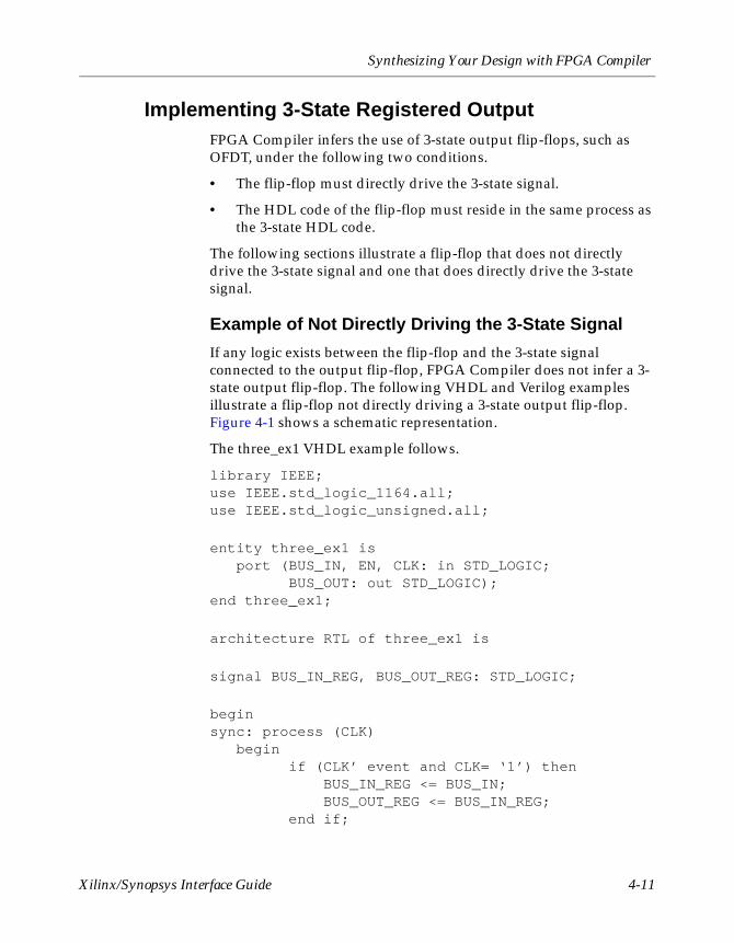
Synthesizing Your Design with FPGA Compiler
Implementing 3-State Registered OutputFPGA Compiler infers the use of 3-state output flip-flops, such as OFDT, under the following two conditions.
• The flip-flop must directly drive the 3-state signal.
• The HDL code of the flip-flop must reside in the same process as the 3-state HDL code.
The following sections illustrate a flip-flop that does not directly drive the 3-state signal and one that does directly drive the 3-state signal.
Example of Not Directly Driving the 3-State Signal
If any logic exists between the flip-flop and the 3-state signal connected to the output flip-flop, FPGA Compiler does not infer a 3-state output flip-flop. The following VHDL and Verilog examples illustrate a flip-flop not directly driving a 3-state output flip-flop. Figure 4-1 shows a schematic representation.
The three_ex1 VHDL example follows.
library IEEE;use IEEE.std_logic_1164.all;use IEEE.std_logic_unsigned.all;
entity three_ex1 is port (BUS_IN, EN, CLK: in STD_LOGIC; BUS_OUT: out STD_LOGIC);end three_ex1;
architecture RTL of three_ex1 is
signal BUS_IN_REG, BUS_OUT_REG: STD_LOGIC;
beginsync: process (CLK) begin if (CLK’ event and CLK= ‘1’) then BUS_IN_REG <= BUS_IN; BUS_OUT_REG <= BUS_IN_REG; end if;
Xilinx/Synopsys Interface Guide 4-11
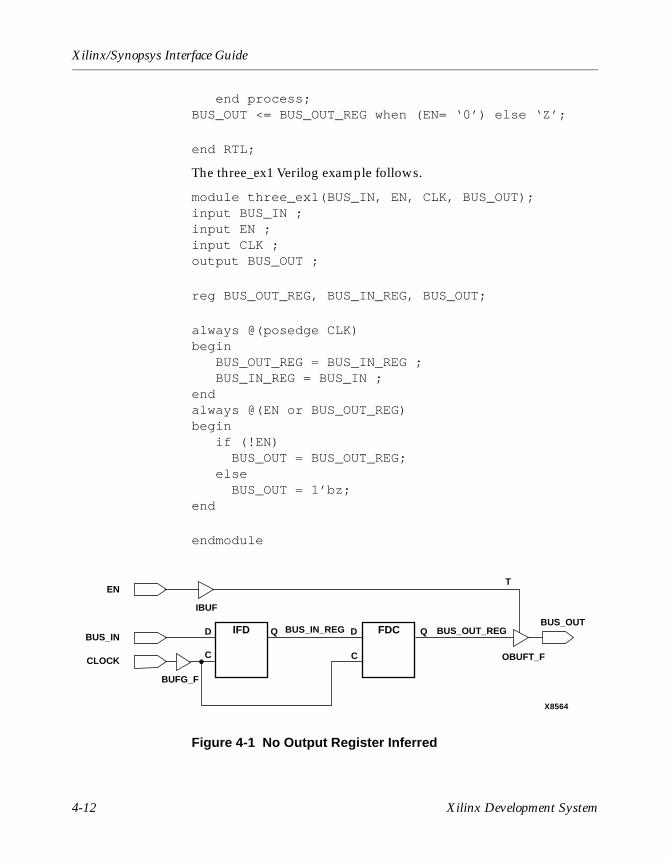
Xilinx/Synopsys Interface Guide
end process;BUS_OUT <= BUS_OUT_REG when (EN= ‘0’) else ‘Z’;
end RTL;
The three_ex1 Verilog example follows.
module three_ex1(BUS_IN, EN, CLK, BUS_OUT);input BUS_IN ;input EN ;input CLK ;output BUS_OUT ;
reg BUS_OUT_REG, BUS_IN_REG, BUS_OUT;
always @(posedge CLK)begin BUS_OUT_REG = BUS_IN_REG ; BUS_IN_REG = BUS_IN ;endalways @(EN or BUS_OUT_REG)begin if (!EN) BUS_OUT = BUS_OUT_REG; else BUS_OUT = 1’bz;end
endmodule
Figure 4-1 No Output Register Inferred
BUS_OUT
OBUFT_F
BUS_OUT_REGBUS_IN
EN
X8564
DBUS_IN_REG
BUFG_F
IBUF
Q
T
FDC
C
D
C
QIFD
CLOCK
4-12 Xilinx Development System
Synthesizing Your Design with FPGA Compiler
Example of Directly Driving the 3-State Signal
The HDL code for the flip-flop must reside in the same process as the 3-state HDL code and must directly drive the 3-state output, as shown in the sync process in the following VHDL and Verilog examples. If the code meets these two conditions, FPGA Compiler infers a registered 3-state output, as illustrated by Figure 4-1.
Having the flip-flop and the 3-state signal in separate processes causes the insertion of additional logic between the flip-flop and the 3-state signal.
The three_ex2 VHDL example follows.
library IEEE;use IEEE.std_logic_1164.all;use IEEE.std_logic_unsigned.all;
entity three_ex2 is port (BUS_IN, EN, CLK: in STD_LOGIC; BUS_OUT: out STD_LOGIC);end three_ex2;
architecture RTL of three_ex2 is
signal BUS_IN_REG: STD_LOGIC;
beginsync: process (CLK, EN) begin if (CLK’ event and CLK= ‘1’) then BUS_IN_REG <= BUS_IN; if (EN= ‘0’) then BUS_OUT <= BUS_IN_REG; else BUS_OUT <= ‘Z’; end if; end if; end process;
end RTL;
The three_ex2 Verilog example follows.
Xilinx/Synopsys Interface Guide 4-13
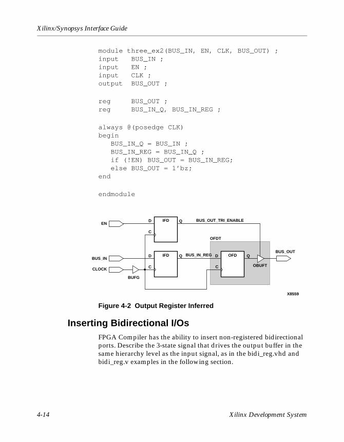
Xilinx/Synopsys Interface Guide
module three_ex2(BUS_IN, EN, CLK, BUS_OUT) ;input BUS_IN ;input EN ;input CLK ;output BUS_OUT ;
reg BUS_OUT ;reg BUS_IN_Q, BUS_IN_REG ;
always @(posedge CLK)begin BUS_IN_Q = BUS_IN ; BUS_IN_REG = BUS_IN_Q ; if (!EN) BUS_OUT = BUS_IN_REG; else BUS_OUT = 1’bz;end
endmodule
Figure 4-2 Output Register Inferred
Inserting Bidirectional I/OsFPGA Compiler has the ability to insert non-registered bidirectional ports. Describe the 3-state signal that drives the output buffer in the same hierarchy level as the input signal, as in the bidi_reg.vhd and bidi_reg.v examples in the following section.
BUS_OUT
OBUFT
OFDT
BUS_IN
EN
X8559
DBUS_IN_REG
BUS_OUT_TRI_ENABLE
BUFG
QOFD
C
D
C
C
D
QIFD
QIFD
CLOCK
4-14 Xilinx Development System
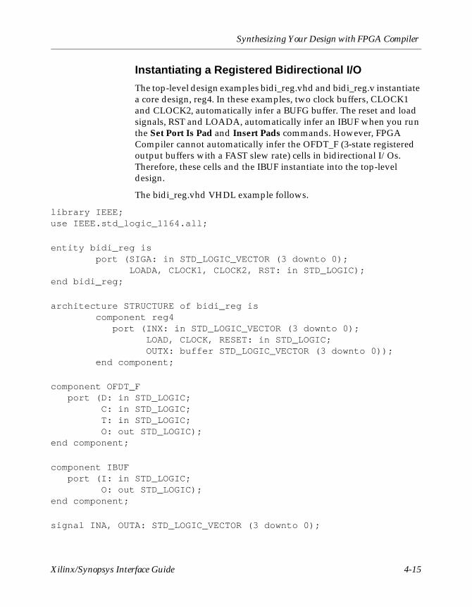
Synthesizing Your Design with FPGA Compiler
Instantiating a Registered Bidirectional I/O
The top-level design examples bidi_reg.vhd and bidi_reg.v instantiate a core design, reg4. In these examples, two clock buffers, CLOCK1 and CLOCK2, automatically infer a BUFG buffer. The reset and load signals, RST and LOADA, automatically infer an IBUF when you run the Set Port Is Pad and Insert Pads commands. However, FPGA Compiler cannot automatically infer the OFDT_F (3-state registered output buffers with a FAST slew rate) cells in bidirectional I/Os. Therefore, these cells and the IBUF instantiate into the top-level design.
The bidi_reg.vhd VHDL example follows.
library IEEE;use IEEE.std_logic_1164.all;
entity bidi_reg is port (SIGA: in STD_LOGIC_VECTOR (3 downto 0); LOADA, CLOCK1, CLOCK2, RST: in STD_LOGIC);end bidi_reg;
architecture STRUCTURE of bidi_reg is component reg4 port (INX: in STD_LOGIC_VECTOR (3 downto 0); LOAD, CLOCK, RESET: in STD_LOGIC; OUTX: buffer STD_LOGIC_VECTOR (3 downto 0)); end component;
component OFDT_F port (D: in STD_LOGIC; C: in STD_LOGIC; T: in STD_LOGIC; O: out STD_LOGIC);end component;
component IBUF port (I: in STD_LOGIC; O: out STD_LOGIC);end component;
signal INA, OUTA: STD_LOGIC_VECTOR (3 downto 0);
Xilinx/Synopsys Interface Guide 4-15
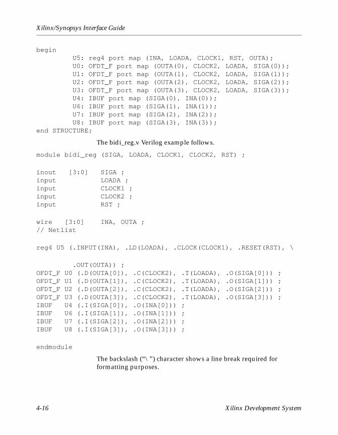
Xilinx/Synopsys Interface Guide
begin U5: reg4 port map (INA, LOADA, CLOCK1, RST, OUTA); U0: OFDT_F port map (OUTA(0), CLOCK2, LOADA, SIGA(0)); U1: OFDT_F port map (OUTA(1), CLOCK2, LOADA, SIGA(1)); U2: OFDT_F port map (OUTA(2), CLOCK2, LOADA, SIGA(2)); U3: OFDT_F port map (OUTA(3), CLOCK2, LOADA, SIGA(3)); U4: IBUF port map (SIGA(0), INA(0)); U6: IBUF port map (SIGA(1), INA(1)); U7: IBUF port map (SIGA(2), INA(2)); U8: IBUF port map (SIGA(3), INA(3));end STRUCTURE;
The bidi_reg.v Verilog example follows.
module bidi_reg (SIGA, LOADA, CLOCK1, CLOCK2, RST) ;
inout [3:0] SIGA ;input LOADA ;input CLOCK1 ;input CLOCK2 ;input RST ;
wire [3:0] INA, OUTA ;// Netlist
reg4 U5 (.INPUT(INA), .LD(LOADA), .CLOCK(CLOCK1), .RESET(RST), \
.OUT(OUTA)) ;OFDT_F U0 (.D(OUTA[0]), .C(CLOCK2), .T(LOADA), .O(SIGA[0])) ;OFDT_F U1 (.D(OUTA[1]), .C(CLOCK2), .T(LOADA), .O(SIGA[1])) ;OFDT_F U2 (.D(OUTA[2]), .C(CLOCK2), .T(LOADA), .O(SIGA[2])) ;OFDT_F U3 (.D(OUTA[3]), .C(CLOCK2), .T(LOADA), .O(SIGA[3])) ;IBUF U4 (.I(SIGA[0]), .O(INA[0])) ;IBUF U6 (.I(SIGA[1]), .O(INA[1])) ;IBUF U7 (.I(SIGA[2]), .O(INA[2])) ;IBUF U8 (.I(SIGA[3]), .O(INA[3])) ;
endmodule
The backslash (“\”) character shows a line break required for formatting purposes.
4-16 Xilinx Development System
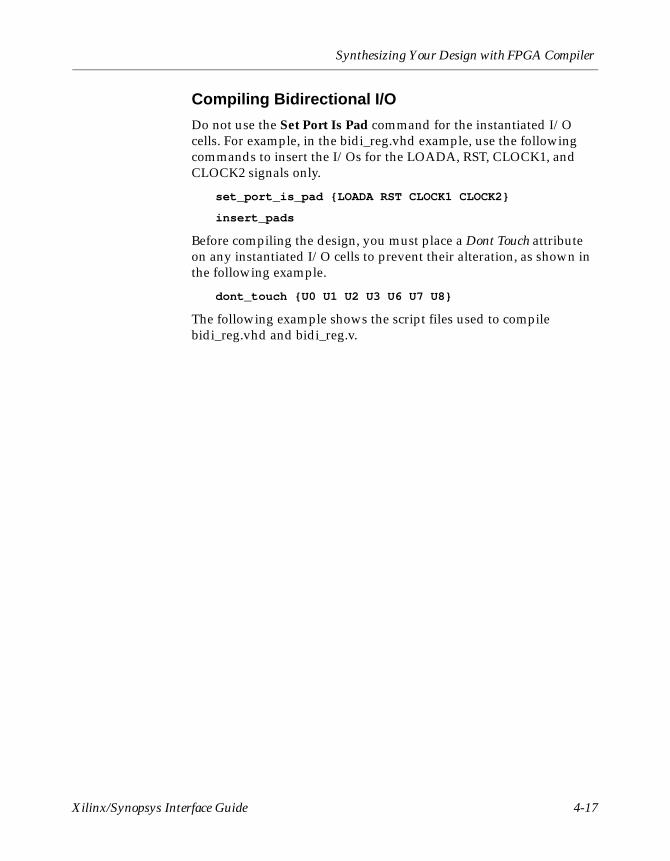
Synthesizing Your Design with FPGA Compiler
Compiling Bidirectional I/O
Do not use the Set Port Is Pad command for the instantiated I/O cells. For example, in the bidi_reg.vhd example, use the following commands to insert the I/Os for the LOADA, RST, CLOCK1, and CLOCK2 signals only.
set_port_is_pad {LOADA RST CLOCK1 CLOCK2}
insert_pads
Before compiling the design, you must place a Dont Touch attribute on any instantiated I/O cells to prevent their alteration, as shown in the following example.
dont_touch {U0 U1 U2 U3 U6 U7 U8}
The following example shows the script files used to compile bidi_reg.vhd and bidi_reg.v.
Xilinx/Synopsys Interface Guide 4-17
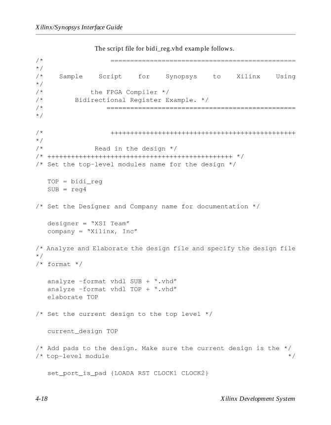
Xilinx/Synopsys Interface Guide
The script file for bidi_reg.vhd example follows.
/* ===============================================*//* Sample Script for Synopsys to Xilinx Using*//* the FPGA Compiler *//* Bidirectional Register Example. *//* ================================================*/
/* +++++++++++++++++++++++++++++++++++++++++++++++*//* Read in the design *//* +++++++++++++++++++++++++++++++++++++++++++++++ *//* Set the top-level modules name for the design */
TOP = bidi_reg SUB = reg4
/* Set the Designer and Company name for documentation */
designer = “XSI Team” company = “Xilinx, Inc”
/* Analyze and Elaborate the design file and specify the design file*//* format */
analyze –format vhdl SUB + “.vhd” analyze –format vhdl TOP + “.vhd” elaborate TOP
/* Set the current design to the top level */
current_design TOP
/* Add pads to the design. Make sure the current design is the *//* top-level module */
set_port_is_pad {LOADA RST CLOCK1 CLOCK2}
4-18 Xilinx Development System
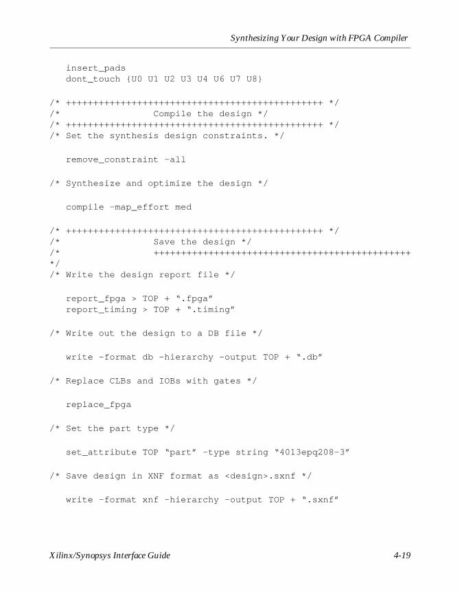
Synthesizing Your Design with FPGA Compiler
insert_pads dont_touch {U0 U1 U2 U3 U4 U6 U7 U8}
/* +++++++++++++++++++++++++++++++++++++++++++++++ *//* Compile the design *//* +++++++++++++++++++++++++++++++++++++++++++++++ *//* Set the synthesis design constraints. */
remove_constraint –all
/* Synthesize and optimize the design */
compile –map_effort med
/* +++++++++++++++++++++++++++++++++++++++++++++++ *//* Save the design *//* +++++++++++++++++++++++++++++++++++++++++++++++*//* Write the design report file */
report_fpga > TOP + “.fpga” report_timing > TOP + “.timing”
/* Write out the design to a DB file */
write –format db –hierarchy –output TOP + “.db”
/* Replace CLBs and IOBs with gates */
replace_fpga
/* Set the part type */
set_attribute TOP “part” –type string “4013epq208-3”
/* Save design in XNF format as <design>.sxnf */
write –format xnf –hierarchy –output TOP + “.sxnf”
Xilinx/Synopsys Interface Guide 4-19
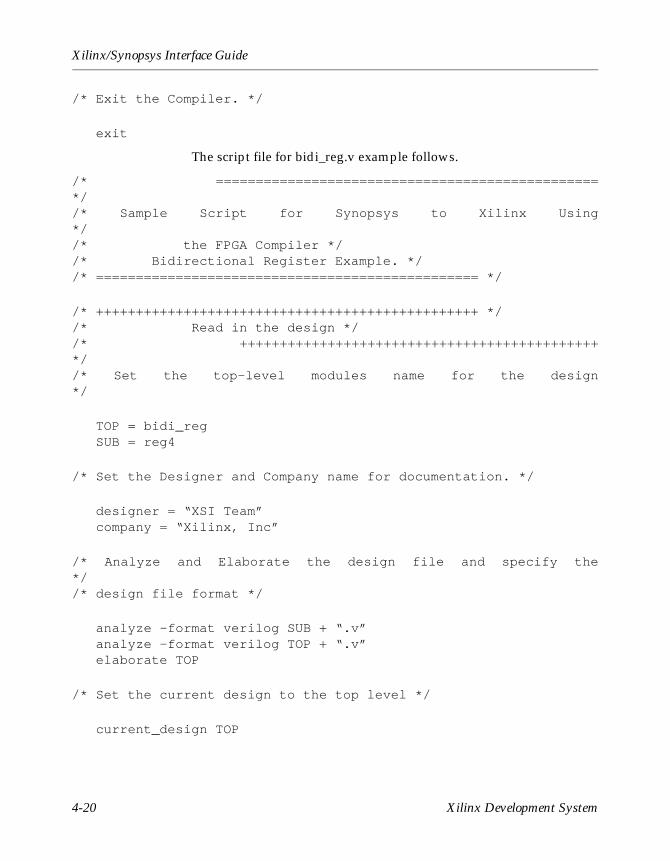
Xilinx/Synopsys Interface Guide
/* Exit the Compiler. */
exit
The script file for bidi_reg.v example follows.
/* ================================================*//* Sample Script for Synopsys to Xilinx Using*//* the FPGA Compiler *//* Bidirectional Register Example. *//* ================================================ */
/* ++++++++++++++++++++++++++++++++++++++++++++++++ *//* Read in the design *//* +++++++++++++++++++++++++++++++++++++++++++++*//* Set the top-level modules name for the design*/
TOP = bidi_reg SUB = reg4
/* Set the Designer and Company name for documentation. */
designer = “XSI Team” company = “Xilinx, Inc”
/* Analyze and Elaborate the design file and specify the*//* design file format */
analyze –format verilog SUB + “.v” analyze –format verilog TOP + “.v” elaborate TOP
/* Set the current design to the top level */
current_design TOP
4-20 Xilinx Development System
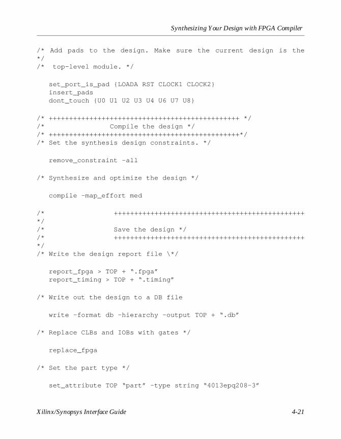
Synthesizing Your Design with FPGA Compiler
/* Add pads to the design. Make sure the current design is the*//* top-level module. */
set_port_is_pad {LOADA RST CLOCK1 CLOCK2} insert_pads dont_touch {U0 U1 U2 U3 U4 U6 U7 U8}
/* +++++++++++++++++++++++++++++++++++++++++++++++ *//* Compile the design *//* +++++++++++++++++++++++++++++++++++++++++++++++*//* Set the synthesis design constraints. */
remove_constraint –all
/* Synthesize and optimize the design */
compile –map_effort med
/* +++++++++++++++++++++++++++++++++++++++++++++++*//* Save the design *//* +++++++++++++++++++++++++++++++++++++++++++++++*//* Write the design report file \*/
report_fpga > TOP + “.fpga” report_timing > TOP + “.timing”
/* Write out the design to a DB file
write –format db –hierarchy –output TOP + “.db”
/* Replace CLBs and IOBs with gates */
replace_fpga
/* Set the part type */
set_attribute TOP “part” –type string “4013epq208-3”
Xilinx/Synopsys Interface Guide 4-21
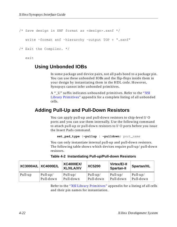
Xilinx/Synopsys Interface Guide
/* Save design in XNF format as <design>.sxnf */
write –format xnf –hierarchy –output TOP + “.sxnf”
/* Exit the Compiler. */
exit
Using Unbonded IOBsIn some package and device pairs, not all pads bond to a package pin. You can use these unbonded IOBs and the flip-flops inside them in your design by instantiating them in the HDL code. However, Synopsys cannot infer unbonded primitives.
A “_U” suffix indicates unbounded primitives. Refer to the “XSI Library Primitives” appendix for a complete listing of all unbonded cells.
Adding Pull-Up and Pull-Down ResistorsYou can apply pull-up and pull-down resistors to chip-level I/O ports and you can use them internally. Use the following command to attach pull-up or pull-down resistors to I/O ports before you issue the Insert Pads command.
set_pad_type {–pullup | –pulldown} port_name
You can only instantiate internal pull-up and pull-down resistors. The following table shows which devices require pull-up/pull-down resistors.
Refer to the “XSI Library Primitives” appendix for a listing of all cells and their pin names for instantiation.
Table 4-2 Instantiating Pull-up/Pull-down Resistors
XC3000A/L XC4000E/LXC4000EX/XL/XLA/XV
XC5200Virtex/E/-II Spartan-II
Spartan/XL
Pull-up Pull-up/Pull-down
Pull-up/Pull-down
Pull-up/Pull-down
Pull-up/Pull-down
Pull-up/Pull-down
4-22 Xilinx Development System
Synthesizing Your Design with FPGA Compiler
See the “Configuring IOBs” section in this chapter for more information on pull-up and pull-down resistors for a specific device family.
Removing the Default Input DelayThe input flip-flops and latches have a default delay preceding the data to the input flip-flop or latch. This delay prevents any possible hold-time violations if you have a clock signal that also comes into the device and clocks the input flip-flop or latch.
You can remove this delay by instantiating a cell that includes the NODELAY attribute if you need additional input speed and have no possibility of a hold-time violation. The “XSI Library Primitives” appendix lists all cells that include a NODELAY attribute. Input flip-flops or latches with an “_F” suffix have a NODELAY attribute assigned to the cell.
Initializing the IOB Flip-Flop to PresetYou can initialize IOB flip-flops to either Clear or Preset in XC3000A/L, XC4000, Spartan and Virtex FPGAs. The default is Clear. To initialize an I/O flip-flop or latch to Preset, use the following command to attach an INIT=S attribute to the flip-flop.
set_attribute “register_name” xnf_init \
“S” type string
Replace register_name with the name of the I/O flip-flop.
You can instantiate I/O cells with the INIT=S attribute already assigned to them. Refer to the “XSI Library Primitives” appendix for a list of all cells and their pin names for instantiation.
Inserting Clock BuffersFor designs with global signals, use global clock buffers to take advantage of the low-skew, high-drive capabilities of the primary global clock buffer (BUFGP) and the secondary global clock buffer (BUFGS). When you use the Insert Pads command, FPGA Compiler automatically inserts a generic global clock buffer (BUFG) whenever an input signal drives a clock signal. The Xilinx implementation software automatically selects the clock buffer
Xilinx/Synopsys Interface Guide 4-23
Xilinx/Synopsys Interface Guide
appropriate for your specified design constraints. If you want to use a specific global buffer, you must instantiate it.
You can instantiate an architecture-specific buffer if you understand the architecture and want to specify how to use the resources. Each XC4000E/L device contains four primary and four secondary global buffers that share the same routing resources. XC4000EX/XL/XLA/XV devices have eight global buffers; each buffer has its own routing resources. For all architectures, use the BUFG for up to four low-skew, high-fanout clock signals.
You can use BUFGS to buffer high-fanout, low-skew signals sourced from inside the FPGA. To access the secondary global clock buffer for an internal signal, instantiate the BUFGS_F cell.
Additionally, you can use BUFGP to distribute signals applied to the FPGA from an external source. A primary global buffer can globally distribute internal signals, however, the signals must drive an external pin.
Controlling Clock Buffer InsertionBecause FPGA Compiler assigns a BUFG to any input signal that drives a clock signal, your design can contain too many clock buffers. The following examples illustrate how to control clock buffer insertion.
The following two examples also illustrate a gated clock using VHDL and Verilog HDL, respectively. By default, Synopsys assigns the signals IN1, IN2, IN3, IN4, and CLK to a BUFG because they ultimately connect to a clock pin.
The gate_clock VHDL example follows.
entity gate_clock is port (IN1, IN2, IN3, IN4, IN5, CLK, LOAD: in BIT; OUT1: buffer BIT);end gate_clock
architecture RTL of gate_clock issignal GATECLK: BIT;beginGATECLK <= not((((IN1 and IN2) and IN3) and IN4) and CLK); process (GATECLK) begin
4-24 Xilinx Development System
Synthesizing Your Design with FPGA Compiler
if (GATECLK’ event and GATECLK= ‘1’) then if (LOAD= ‘1’) then OUT1 <= IN5; else OUT1 <= OUT1; end if; end if; end process;end RTL;
The gate_clock Verilog HDL example follows.
module gate_clock(IN1, IN2, IN3, IN4, IN5, CLK, LOAD, OUT1) ;input IN1 ;input IN2 ;input IN3 ;input IN4 ;input IN5 ;input CLK ;input LOAD ;output OUT1;
reg OUT1;
wire GATECLK ;
assign GATECLK = ~(IN1 & IN2 & IN3 & IN4 & CLK) ;
always @(posedge GATECLK)begin if (LOAD == 1’b1) OUT1 = IN5 ;end
endmodule
FPGA Compiler identifies clock ports by tracing back from the clock pins on the flip-flops. In the following figure, the inputs to the 5-input NAND gate all have a BUFG inserted.
Xilinx/Synopsys Interface Guide 4-25
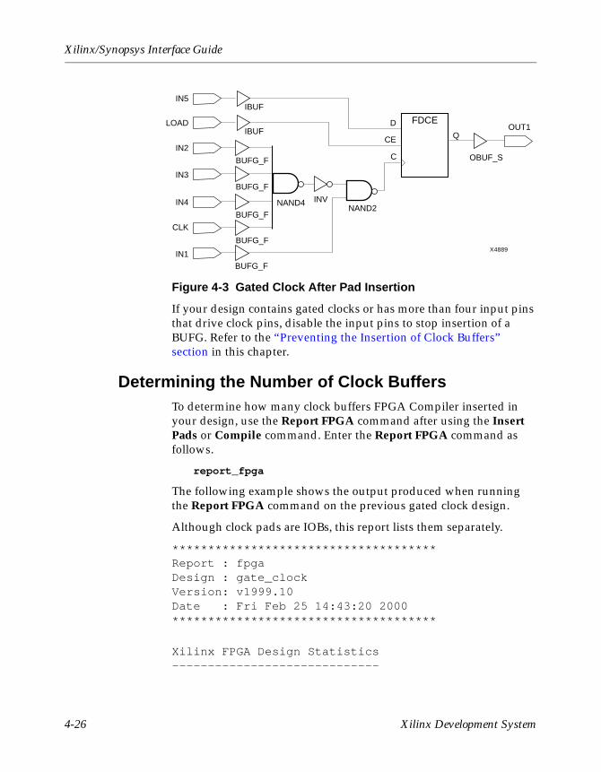
Xilinx/Synopsys Interface Guide
Figure 4-3 Gated Clock After Pad Insertion
If your design contains gated clocks or has more than four input pins that drive clock pins, disable the input pins to stop insertion of a BUFG. Refer to the “Preventing the Insertion of Clock Buffers” section in this chapter.
Determining the Number of Clock BuffersTo determine how many clock buffers FPGA Compiler inserted in your design, use the Report FPGA command after using the Insert Pads or Compile command. Enter the Report FPGA command as follows.
report_fpga
The following example shows the output produced when running the Report FPGA command on the previous gated clock design.
Although clock pads are IOBs, this report lists them separately.
*************************************Report : fpgaDesign : gate_clockVersion: v1999.10Date : Fri Feb 25 14:43:20 2000*************************************
Xilinx FPGA Design Statistics-----------------------------
OUT1
OBUF_S
IBUFIN5
LOAD
IN2
IN3
IN4
CLK
IN1
IBUF
BUFG_F
BUFG_F
BUFG_F
BUFG_F
BUFG_F
NAND4NAND2
INV
X4889
CE Q
FDCE
C
D
4-26 Xilinx Development System
Synthesizing Your Design with FPGA Compiler
FG Function Generators 1H Function Generators 1Number of CLB cells: 1Number of Hard Macros and Other Cells: 0Number of CLBs in Other Cells: 0Total Number of CLBs: 1
Number of Ports: 8Number of Clock Pads: 5Number of IOBs: 3
Number of Flip Flops: 1Number of 3-State Buffers: 0
Total Number of Cells: 9
Preventing the Insertion of Clock BuffersTo prevent FPGA Compiler from inserting the BUFG primitive, specify the Set Pad Type command with the following options before inserting the pads.
set_pad_type –no_clock {clock_ports}
Replace clock_ports with the name of the input pins where you do not want a clock buffer inserted. For the gated clock VHDL and Verilog examples, enter the following.
set_pad_type –no_clock {IN1, IN2, IN3, IN4, CLK}
Then follow the normal procedures to set the ports as pads and insert the pads as follows.
set_port_is_pad “*”
insert_pads
Using MemoryYou can use on-chip RAM for status registers, index registers, counter storage, distributed shift registers, LIFO stacks, and FIFO buffers.
Xilinx/Synopsys Interface Guide 4-27
Xilinx/Synopsys Interface Guide
The XC4000 family can efficiently implement RAM and ROM using CLB function generators. Implement a ROM by describing it behaviorally as shown in the “Implementing XC4000 RAMs” section. Alternatively, the XSI XC4000 libraries contain 16 x 1 (16 deep x 1 wide) and 32 x 1 (32 deep x 1 wide) RAM and ROM primitives and 16 x 1 dual-port RAM you can instantiate.
You can also implement memory using the LogiBLOX program. LogiBLOX can create RAM and ROM between 1–32 bits wide and 2–256 bits deep. Using LogiBLOX to add RAM or ROM to your design provides an efficient implementation of your memory in addition to a simulation model for Register Transfer Level (RTL) simulation.
For VHDL and Verilog examples of instantiating RAM in your designs using LogiBLOX, refer to the “Using CORE Generator and LogiBLOX” chapter. Also, refer to the LogiBLOX Guide for more information on LogiBLOX.
Implementing XC4000 RAMsImplement RAMs in your HDL with the following methods.
• Instantiate 16 x 1 and 32 x 1 RAMs from the XSI primitive libraries.
• Instantiate any size RAM using LogiBLOX.
Behaviorally describing RAMs in VHDL creates combinatorial loops during compiling.
4-28 Xilinx Development System
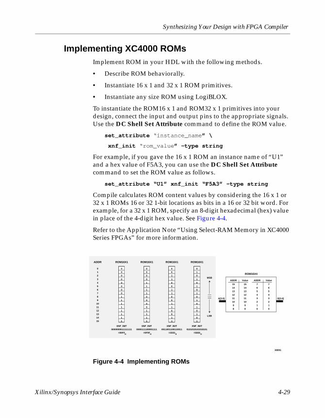
Synthesizing Your Design with FPGA Compiler
Implementing XC4000 ROMsImplement ROM in your HDL with the following methods.
• Describe ROM behaviorally.
• Instantiate 16 x 1 and 32 x 1 ROM primitives.
• Instantiate any size ROM using LogiBLOX.
To instantiate the ROM16 x 1 and ROM32 x 1 primitives into your design, connect the input and output pins to the appropriate signals. Use the DC Shell Set Attribute command to define the ROM value.
set_attribute “instance_name” \
xnf_init “rom_value” –type string
For example, if you gave the 16 x 1 ROM an instance name of “U1” and a hex value of F5A3, you can use the DC Shell Set Attribute command to set the ROM value as follows.
set_attribute “U1” xnf_init “F5A3” –type string
Compile calculates ROM content values by considering the 16 x 1 or 32 x 1 ROMs 16 or 32 1-bit locations as bits in a 16 or 32 bit word. For example, for a 32 x 1 ROM, specify an 8-digit hexadecimal (hex) value in place of the 4-digit hex value. See Figure 4-4.
Refer to the Application Note “Using Select-RAM Memory in XC4000 Series FPGAs” for more information.
Figure 4-4 Implementing ROMs
0
1
2
3
4
5
6
7
8
9
10
11
12
13
14
15
ADDR
0
0
0
0
0
0
0
0
1
1
1
1
1
1
1
1
ROM16X1
XNF_INIT0000000011111111
=00FFH
0
0
0
0
1
1
1
1
0
0
0
0
1
1
1
1
ROM16X1
XNF_INIT0000111100001111
=0F0FH
0
0
1
1
0
0
1
1
0
0
1
1
0
0
1
1
ROM16X1
XNF_INIT0011001100110011
=3333H
0
1
0
1
0
1
0
1
0
1
0
1
0
1
0
1
ROM16X1
XNF_INIT0101010101010101
=5555H
MSB
LSB
15
14
13
12
11
10
9
8
ADDR
15
14
13
12
11
10
9
8
Value
7
6
5
4
3
2
1
0
ADDR
7
6
5
4
3
2
1
0
Value
A[3:0] O[3:0]
ROM16X4
X8001
Xilinx/Synopsys Interface Guide 4-29
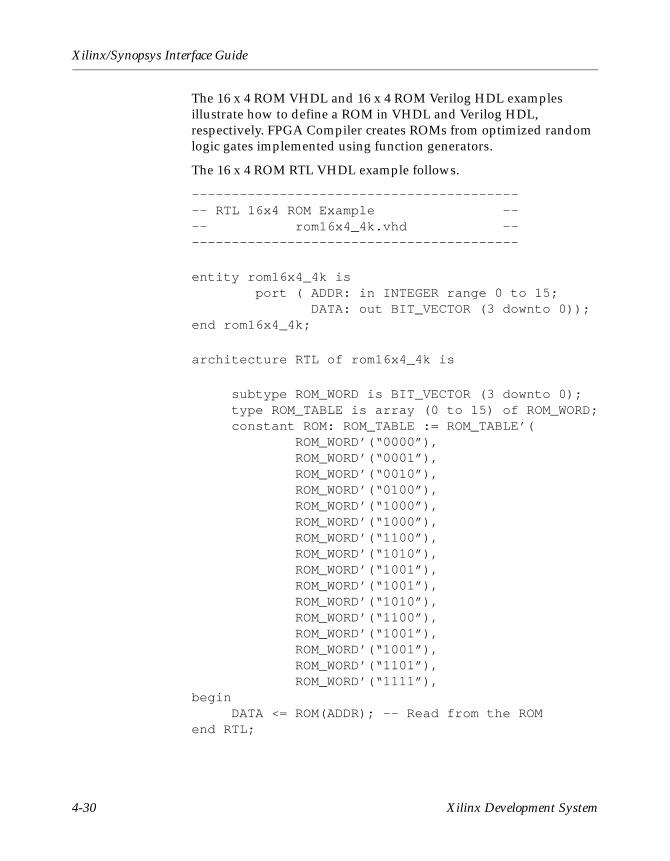
Xilinx/Synopsys Interface Guide
The 16 x 4 ROM VHDL and 16 x 4 ROM Verilog HDL examples illustrate how to define a ROM in VHDL and Verilog HDL, respectively. FPGA Compiler creates ROMs from optimized random logic gates implemented using function generators.
The 16 x 4 ROM RTL VHDL example follows.
------------------------------------------- RTL 16x4 ROM Example ---- rom16x4_4k.vhd -------------------------------------------
entity rom16x4_4k is port ( ADDR: in INTEGER range 0 to 15; DATA: out BIT_VECTOR (3 downto 0));end rom16x4_4k;
architecture RTL of rom16x4_4k is
subtype ROM_WORD is BIT_VECTOR (3 downto 0); type ROM_TABLE is array (0 to 15) of ROM_WORD; constant ROM: ROM_TABLE := ROM_TABLE’( ROM_WORD’(“0000”), ROM_WORD’(“0001”), ROM_WORD’(“0010”), ROM_WORD’(“0100”), ROM_WORD’(“1000”), ROM_WORD’(“1000”), ROM_WORD’(“1100”), ROM_WORD’(“1010”), ROM_WORD’(“1001”), ROM_WORD’(“1001”), ROM_WORD’(“1010”), ROM_WORD’(“1100”), ROM_WORD’(“1001”), ROM_WORD’(“1001”), ROM_WORD’(“1101”), ROM_WORD’(“1111”),begin DATA <= ROM(ADDR); -- Read from the ROMend RTL;
4-30 Xilinx Development System
Synthesizing Your Design with FPGA Compiler
The 16 x 4 ROM RTL Verilog example follows.
module rom16x4_4k(ADDR, DATA) ;input [3:0] ADDR ;output [3:0] DATA ;
reg [3:0] DATA ;
always @(ADDR)begin case (ADDR) 4’b0000 : DATA = 4’b0000 ; 4’b0001 : DATA = 4’b0001 ; 4’b0010 : DATA = 4’b0010 ; 4’b0011 : DATA = 4’b0100 ; 4’b0100 : DATA = 4’b1000 ; 4’b0101 : DATA = 4’b1000 ; 4’b0110 : DATA = 4’b1100 ; 4’b0111 : DATA = 4’b1010 ; 4’b1000 : DATA = 4’b1001 ; 4’b1001 : DATA = 4’b1001 ; 4’b1010 : DATA = 4’b1010 ; 4’b1011 : DATA = 4’b1100 ; 4’b1100 : DATA = 4’b1001 ; 4’b1101 : DATA = 4’b1001 ; 4’b1110 : DATA = 4’b1101 ; 4’b1111 : DATA = 4’b1111 ; endcaseend
endmodule
Implementing RAM In Virtex DevicesThe INIT values for RAM32X 1 and RAM32X1_1 map differently from 4000EX/XL/XV and SpartanXL.
Virtex maps the lower INIT values to G and upper INIT values to F for both RAM32X. 4000EX/XL/XV and SpartanXL map those lower INIT values to F and upper INIT values to G.
Xilinx/Synopsys Interface Guide 4-31
Xilinx/Synopsys Interface Guide
Performing Boundary ScanThe XC4000, XC5200, Spartan, and Virtex FPGA devices contain boundary-scan facilities compatible with IEEE Standard 1149.1. Refer to the Development System Reference Guide for a detailed description of the XC4000 and XC5200 boundary scan capabilities.
Xilinx parts support external (I/O and interconnect) testing and have limited support for internal self-test.
Full access to the built-in boundary-scan logic exists between power-up and the start of configuration. Optionally, specify boundary scan in the design to access built-in logic after configuration. During configuration, you can use the Sample/Preload and Bypass instructions only.
To make boundary-scan logic active in a configured FPGA device, include the boundary-scan cell and its related I/O cells in the configuration data of your design. For HDL designs, you must instantiate the boundary-scan symbol, BSCAN, and the boundary scan I/O pins, TDI, TMS, TCK, and TDO.
Warning: Do not use the following FPGA Compiler boundary scan commands because they do not work with FPGA devices.
set jtag implementation
set jtag instruction
set jtag port
The following figure illustrates the BSCAN symbol instantiated into an HDL design.
4-32 Xilinx Development System
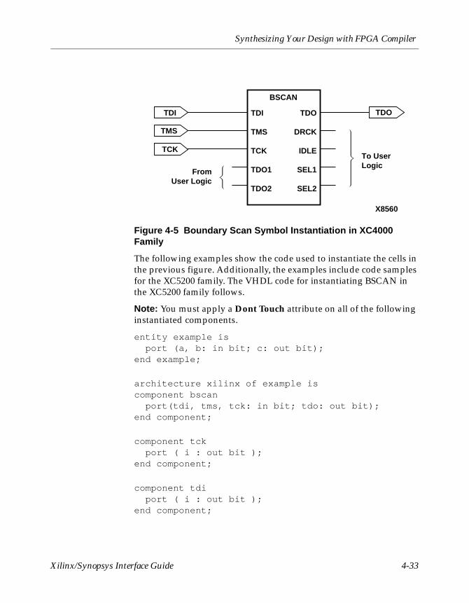
Synthesizing Your Design with FPGA Compiler
Figure 4-5 Boundary Scan Symbol Instantiation in XC4000 Family
The following examples show the code used to instantiate the cells in the previous figure. Additionally, the examples include code samples for the XC5200 family. The VHDL code for instantiating BSCAN in the XC5200 family follows.
Note: You must apply a Dont Touch attribute on all of the following instantiated components.
entity example is port (a, b: in bit; c: out bit);end example;
architecture xilinx of example iscomponent bscan port(tdi, tms, tck: in bit; tdo: out bit);end component;
component tck port ( i : out bit );end component;
component tdi port ( i : out bit );end component;
TDI
TMS
TCK
TDO1
TDO2
TDO
DRCK
IDLE
SEL1
SEL2
TDI
TMS
TCK
TDO
BSCAN
FromUser Logic
To UserLogic
X8560
Xilinx/Synopsys Interface Guide 4-33
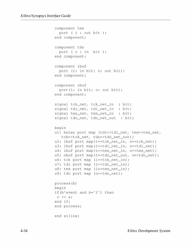
Xilinx/Synopsys Interface Guide
component tms port ( i : out bit );end component;
component tdo port ( o : in bit );end component;
component ibuf port (i: in bit; o: out bit);end component;
component obuf port(i: in bit; o: out bit);end component;
signal tck_net, tck_net_in : bit;signal tdi_net, tdi_net_in : bit;signal tms_net, tms_net_in : bit;signal tdo_net, tdo_net_out : bit;
beginu1: bscan port map (tdi=>tdi_net, tms=>tms_net,
tck=>tck_net, tdo=>tdo_net_out);u2: ibuf port map(i=>tck_net_in, o=>tck_net);u3: ibuf port map(i=>tdi_net_in, o=>tdi_net);u4: ibuf port map(i=>tms_net_in, o=>tms_net);u5: obuf port map(i=>tdo_net_out, o=>tdo_net);u6: tck port map (i=>tck_net_in);u7: tdi port map (i=>tdi_net_in);u8: tms port map (i=>tms_net_in);u9: tdo port map (o=>tdo_net);
process(b)beginif(b’event and b=’1’) then c <= a;end if;end process;
end xilinx;
4-34 Xilinx Development System
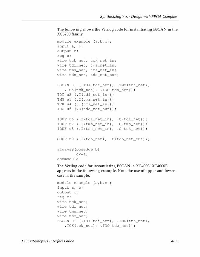
Synthesizing Your Design with FPGA Compiler
The following shows the Verilog code for instantiating BSCAN in the XC5200 family.
module example (a,b,c);input a, b;output c;reg c;wire tck_net, tck_net_in;wire tdi_net, tdi_net_in;wire tms_net, tms_net_in;wire tdo_net, tdo_net_out;
BSCAN u1 (.TDI(tdi_net), .TMS(tms_net), .TCK(tck_net), .TDO(tdo_net));
TDI u2 (.I(tdi_net_in));TMS u3 (.I(tms_net_in));TCK u4 (.I(tck_net_in));TDO u5 (.O(tdo_net_out));
IBUF u6 (.I(tdi_net_in), .O(tdi_net));IBUF u7 (.I(tms_net_in), .O(tms_net));IBUF u8 (.I(tck_net_in), .O(tck_net));
OBUF u9 (.I(tdo_net), .O(tdo_net_out));
always@(posedge b) c<=a;endmodule
The Verilog code for instantiating BSCAN in XC4000/XC4000E appears in the following example. Note the use of upper and lower case in the sample.
module example (a,b,c);input a, b;output c;reg c;wire tck_net;wire tdi_net;wire tms_net;wire tdo_net;BSCAN u1 (.TDI(tdi_net), .TMS(tms_net),
.TCK(tck_net), .TDO(tdo_net));
Xilinx/Synopsys Interface Guide 4-35
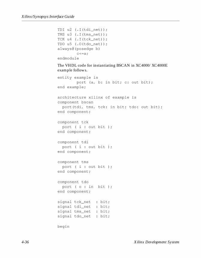
Xilinx/Synopsys Interface Guide
TDI u2 (.I(tdi_net));TMS u3 (.I(tms_net));TCK u4 (.I(tck_net));TDO u5 (.O(tdo_net));always@(posedge b) c<=a;endmodule
The VHDL code for instantiating BSCAN in XC4000/XC4000E example follows.
entity example is port (a, b: in bit; c: out bit);end example;
architecture xilinx of example iscomponent bscan port(tdi, tms, tck: in bit; tdo: out bit);end component;
component tck port ( i : out bit );end component;
component tdi port ( i : out bit );end component;
component tms port ( i : out bit );end component;
component tdo port ( o : in bit );end component;
signal tck_net : bit;signal tdi_net : bit;signal tms_net : bit;signal tdo_net : bit;
begin
4-36 Xilinx Development System
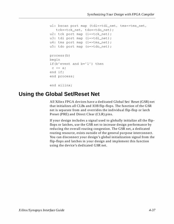
Synthesizing Your Design with FPGA Compiler
u1: bscan port map (tdi=>tdi_net, tms=>tms_net, tck=>tck_net, tdo=>tdo_net);
u2: tck port map (i=>tck_net);u3: tdi port map (i=>tdi_net);u4: tms port map (i=>tms_net);u5: tdo port map (o=>tdo_net);
process(b)beginif(b’event and b=’1’) then c <= a;end if;end process;
end xilinx;
Using the Global Set/Reset NetAll Xilinx FPGA devices have a dedicated Global Set/Reset (GSR) net that initializes all CLBs and IOB flip-flops. The function of the GSR net is separate from and overrides the individual flip-flop or latch Preset (PRE) and Direct Clear (CLR) pins.
If your design includes a signal used to globally initialize all the flip-flops or latches, use the GSR net to increase design performance by reducing the overall routing congestion. The GSR net, a dedicated routing resource, exists outside of the general purpose interconnect. You can disconnect your design’s global initialization signal from the flip-flops and latches in your design and implement this function using the device’s dedicated GSR net.
Xilinx/Synopsys Interface Guide 4-37
Xilinx/Synopsys Interface Guide
Figure 4-6 Emulation of Power-on State “1” with Inverters (XC3000A/L, XC3100A, and XC5200)
Accessing Global Set/Reset Using STARTBUFAccess an FPGA’s GSR signal by attaching a net to the input pin on the STARTBUF cell. Asserting the net attached to the STARTBUF block’s GSR pin also asserts FPGA Global Set/Reset causing every flip-flop and latch in the device to assume its power-on state.
You must instantiate the STARTBUF block.
The GSR net does not appear in the pre-placed and routed netlist. Asserting the GSR signal to High (the default) sets every flip-flop and latch to the same state it had at the end of configuration, illustrated in the following tables. When you simulate the placed and routed design, the simulator’s translation program correctly inserts the functionality.
Any signal can drive the STARTUP block’s GSR pin, however, do not use flip-flop or latch output signals.
CLK
QD
CLR
PRE
QD
C
X8003
4-38 Xilinx Development System
Synthesizing Your Design with FPGA Compiler
Synthesizing/Simulating for VHDL Global Set/Reset Emulation
VHDL requires a testbench to control all signal ports. You can instantiate certain VHDL-specific components, explained in the following sections, in the RTL and post-synthesis VHDL description to allow the simulation of the global signals for global set/reset and global 3-state.
NGD2VHDL creates a port in your back-annotated design entity for stimulating the global set/reset or 3-state enable signals. This port does not actually exist on the configured part.
When running NGD2VHDL, you do not need to use the –gp switch to create an external port if you instantiate a STARTUP block in your implemented design. The port is already identified and connected to the global set/reset or 3-state enable signal. If you do not use the –gp option or a STARTBUF block, you must use special components, as described in the following sections.
Using STARTBUF in VHDL
STARTBUF replaces STARTUP. With STARTBUF you can functionally simulate the GSR/GR net in both function and timing simulation. By connecting the input pin of the STARTBUF to a top-level port and using STARTBUF as the source for all asynchronous set/reset signals in a design, Xilinx software can automatically optimize the design to use the GSR/GR. Because you can use STARTBUF in functional simulation (unlike STARTUP), when you use STARTBUF you can map to the GSR/GR in a device. You can still use STARTUP, but it does not always provide correct GSR/GR in HDL flows.
The STARTBUF component passes a reset or 3-state signal in the same way that a buffer allows simulation to proceed and also instantiates the STARTUP block for implementation. One version of STARTBUF works for all devices, however, the XC5200 and the XC4000 STARTUP blocks have different pin names. Implementation with the correct STARTUP block occurs automatically. The following shows an instantiation example of the STARTBUF component.
U1: STARTBUF port map (GSRIN => DEV_GSR_PORT, GTSIN =>DEV_GTS_PORT, CLKIN => ‘0’, GSROUT => GSR_NET,
Xilinx/Synopsys Interface Guide 4-39
Xilinx/Synopsys Interface Guide
GTSOUT => GTS_NET, Q2OUT => open, Q3OUT => open, Q1Q4OUT => open, DONEINOUT => open):
You can use one or both of the input ports (GSRIN and GTSIN) of the STARTBUF component and the associated output ports (GSROUT and GTSOUT). You can use pins left open to pass configuration instructions to the implementation tools by connecting the appropriate signal to the port instead of leaving it open.
Instantiating a STARTUP Block in VHDL
The STARTUP block traditionally instantiates to identify the GR, PRLD, or GSR signals for implementation. However, simulation can occur only when the net attached to the GSR or GTS goes off the chip because the STARTUP block does not have a simulation model. You can use the new components described below to simulate global set/reset or 3-state nets whether or not the signal goes off the chip.
Setting Direct Preset or Direct ClearYou can program each flip-flop and latch as either Preset or Clear but not both. The device’s automatic assertion of its own GSR net asynchronously sets flip-flops and latches as either Preset or Cleared upon completion of configuration. Use individual flip-flop and latch Preset (PRE) and Clear (CLR) pins to set them as preset or cleared.
The power-on state of a register or latch and the selection of PRE or CLR pin must match. For example, a register with a CLR pin assumes the value of 0 on power-up. Alternatively, a register with a power-up state of 0 can only have a CLR pin.
To get an asynchronous set or asynchronous reset flip-flop, describe the behavior in the RTL code. If you only want to describe the power-on state of an flip-flop, connect the asynchronous set or asynchronous reset signal of the RTL flip-flop to the ROCBUF.
Increasing Performance with the GSR NetMany designs have a net that initializes the majority of the design’s flip-flops. If this signal initializes all the design’s flip-flops, you can use the GSR net.
4-40 Xilinx Development System
Synthesizing Your Design with FPGA Compiler
To have your HDL simulation match that of the resulting design, modify your HDL code so that asserting the GSR signal presets or clears every flip-flop and latch. You must ensure that this signal does not get routed around general purpose interconnect but instead uses the dedicated global routing resource. Disconnect this signal with the Disconnect Net command after you compile your design but before you save it.
Alternatively, the Xilinx tools move this signal on to the device’s dedicated GSR routing network when the following conditions apply.
• The asynchronous Preset or Clear pin of every register in your design that has this pin connects to the same net.
• That net connects to the GSR pin of the STARTUP block.
• You use STARTBUF (see the “Using the Global Set/Reset Net” section).
The following figure illustrates this flow.
Figure 4-7 Increasing Performance with GSR Net
CLK
QD
CLK
QD
CLK
QD
IBUF
CLK
CLR CLR
QD
CLK
QD QD FDC
FDC FDP FDC
PRE
IBUFPORTRESET
PORTRESET
RESETNET
STARTUP
GSR
CLK
STARTUP
GSR
X8002
Xilinx/Synopsys Interface Guide 4-41
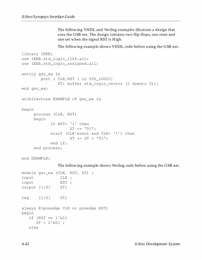
Xilinx/Synopsys Interface Guide
The following VHDL and Verilog examples illustrate a design that uses the GSR net. The design contains two flip-flops, one reset and one set when the signal RST is High.
The following example shows VHDL code before using the GSR net.
library IEEE;use IEEE.std_logic_1164.all;use IEEE.std_logic_unsigned.all;
entity gsr_ex is port ( CLK,RST : in STD_LOGIC; ST: buffer std_logic_vector (1 downto 0));end gsr_ex;
architecture EXAMPLE of gsr_ex is
begin process (CLK, RST) begin if RST= ‘1’ then ST <= “01”; elsif (CLK’event and CLK= ‘1’) then ST <= ST + “01”; end if; end process;
end EXAMPLE;
The following example shows Verilog code before using the GSR net.
module gsr_ex (CLK, RST, ST) ;input CLK ;input RST ;output [1:0] ST;
reg [1:0] ST;
always @(posedge CLK or posedge RST)begin if (RST == 1’b1) ST = 2’b01 ; else
4-42 Xilinx Development System
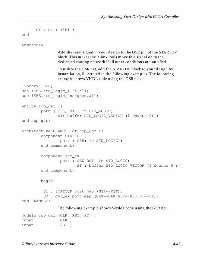
Synthesizing Your Design with FPGA Compiler
ST = ST + 1’b1 ;end
endmodule
Add the reset signal in your design to the GSR pin of the STARTUP block. This makes the Xilinx tools move this signal on to the dedicated routing network if all other conditions are satisfied.
To utilize the GSR net, add the STARTUP block to your design by instantiation, illustrated in the following examples. The following example shows VHDL code using the GSR net.
library IEEE;use IEEE.std_logic_1164.all;use IEEE.std_logic_unsigned.all;
entity top_gsr is port ( CLK,RST : in STD_LOGIC; ST: buffer STD_LOGIC_VECTOR (1 downto 0));end top_gsr;
architecture EXAMPLE of top_gsr is component STARTUP port ( GSR: in STD_LOGIC); end component;
component gsr_ex port ( CLK,RST: in STD_LOGIC; ST : buffer STD_LOGIC_VECTOR (1 downto 0)); end component;
begin
U1 : STARTUP port map (GSR=>RST); U2 : gsr_ex port map (CLK=>CLK,RST=>RST,ST=>ST);end EXAMPLE;
The following example shows Verilog code using the GSR net.
module top_gsr (CLK, RST, ST) ;input CLK ;input RST ;
Xilinx/Synopsys Interface Guide 4-43
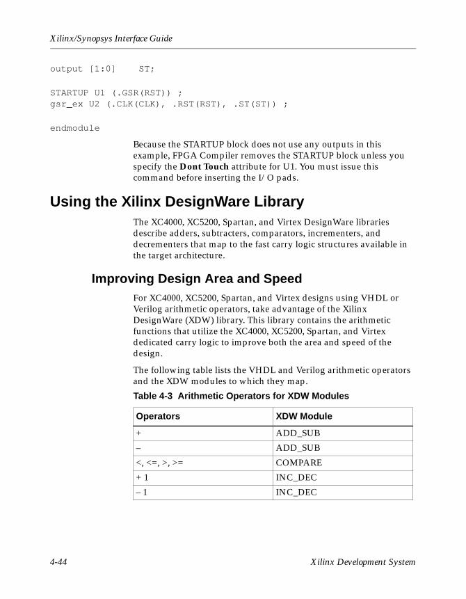
Xilinx/Synopsys Interface Guide
output [1:0] ST;
STARTUP U1 (.GSR(RST)) ;gsr_ex U2 (.CLK(CLK), .RST(RST), .ST(ST)) ;
endmodule
Because the STARTUP block does not use any outputs in this example, FPGA Compiler removes the STARTUP block unless you specify the Dont Touch attribute for U1. You must issue this command before inserting the I/O pads.
Using the Xilinx DesignWare LibraryThe XC4000, XC5200, Spartan, and Virtex DesignWare libraries describe adders, subtracters, comparators, incrementers, and decrementers that map to the fast carry logic structures available in the target architecture.
Improving Design Area and SpeedFor XC4000, XC5200, Spartan, and Virtex designs using VHDL or Verilog arithmetic operators, take advantage of the Xilinx DesignWare (XDW) library. This library contains the arithmetic functions that utilize the XC4000, XC5200, Spartan, and Virtex dedicated carry logic to improve both the area and speed of the design.
The following table lists the VHDL and Verilog arithmetic operators and the XDW modules to which they map.
Table 4-3 Arithmetic Operators for XDW Modules
Operators XDW Module
+ ADD_SUB
– ADD_SUB
<, <=, >, >= COMPARE
+ 1 INC_DEC
– 1 INC_DEC
4-44 Xilinx Development System
Synthesizing Your Design with FPGA Compiler
The XDW library contains twos complement and unsigned binary modules of widths 6, 8, 10, 12, 14, 16, 20, 24, 28, 32, and 48. Additionally, you can use available 64-bit widths for the COMPARE module only. Operands falling between bit ranges map to the next higher bit-width module. The Xilinx design implementation tools remove any unused logic when implementing a smaller bit width or when adding, subtracting, or comparing with a constant value.
The XDW library contains area and speed information for its modules. This information allows FPGA Compiler and Design Compiler to compare XDW implementations of arithmetic functions to other DesignWare libraries available at compile time. XSI then selects the implementation that best meets your timing and area constraints.
XC4000, Spartan and Virtex devices accommodate two bits of arithmetic function per CLB, and XC5200 devices accommodate four bits per CLB. XC4000, Spartan, and Virtex devices implement arithmetic functions in one vertical column of CLBs. The carry propagation direction is upward in XC4000EX/XL/XLA/XV, Spartan, and Virtex devices and up or down in XC4000E/L devices. XC5200 devices implement arithmetic functions in two vertical columns of CLBs and have an upward carry propagation direction.
The Xilinx place and route tools determine the best placement for the CLB columns in the target device and break or wrap a column if constrained by the physical boundaries of the device. However, as a general rule, choose a target device that can accommodate the “tallest” arithmetic structure in your design without altering the shape of this structure. Selecting the correct device makes it easier to place and route predominately data path-based designs.
Creating Timing SpecificationsThe timing constraints issued to Synopsys to control the synthesis process pass through to the design implementation tools to control the place and route process. To get the best possible results, make these constraints realistic and achievable.
During the synthesis of your design, area and timing constraints can impact implementation almost as much as changes made to your HDL code. Carefully apply area and timing constraints. During the implementation of your design, timing constraints have a direct impact on run time and performance verification. For example, the
Xilinx/Synopsys Interface Guide 4-45
Xilinx/Synopsys Interface Guide
run time required to find a place and route solution to support the 40 MHz operation of a design takes longer than that required to find a 4 MHz solution. Meaningful and detailed timing constraints also allow the design implementation tools to report the status of your design’s timing in terms of your timing goals.
The DC2NCF program converts timing constraints applied to your design in the Synopsys environment to equivalent constraints that control the Xilinx place and route process. Automatic translation of these constraints offers an advantage because you do not need to apply the constraints twice (once for Synopsys and again for Xilinx). The constraints used by Xilinx are equivalent to those applied with Synopsys.
DC2NCF supports translation of the following Synopsys timing constraints.
• create_clock
• set_input_delay
• set_output_delay
• set_max_delay
• set_false_path
If you have additional Synopsys timing constraint commands in your Synopsys script file, DC2NCF issues a warning and does not translate them.
4-46 Xilinx Development System
Synthesizing Your Design with FPGA Compiler
DC2NCF translates a Synopsys DC file to a Xilinx Netlist Constraints File (NCF). The DC file is a Synopsys script file containing the constraints that have been applied to your design. EDIF2NGD or XNF2NGD reads the output NCF file. The constraints in the NCF file become part of the NGO file produced by EDIF2NGD or XNF2NGD. The following example shows how to translate a DC file to an NCF file.
dc2ncf dc_file[.dc] [–o ncf_file[.ncf]] [–w | –wildcard]
Note Braces “{“, should not be used in the DC2NCF command line syntax.
When you specify the –w option, DC2NCF creates an NCF file with wildcards. The –w option can significantly increase run time. An NCF backup file without wildcards saves as ncf_file.ncf_orig. To use the original file without wildcards, rename ncf_file.ncf_orig to ncf_file.ncf.
Following the DC2NCF Design FlowBefore running DC2NCF, apply your timing constraints to your design and then compile it. Also, when using FPGA Compiler for XC4000 designs, run the Replace FPGA command, then create a netlist and a corresponding script file that contains the constraints.
DC2NCF can incorrectly translate the timing constraint commands in user-created script files. Always generate script files as described in the following sections using either DC Shell or Design Analyzer.
Creating the Netlist and Script File (Design Compiler)
You can use DC Shell or Design Analyzer to create your design’s netlist and the Synopsys constraints script file.
From the DC Shell command line, perform the following steps.
1. Flatten your design’s hierarchy by entering the following.
ungroup –all –flatten
2. Enter the following to create the netlist.
write –format edif –hierarchy –output \
design_name.sedif
Xilinx/Synopsys Interface Guide 4-47
Xilinx/Synopsys Interface Guide
The “\” indicates you issue this command in one line, not two as presented here.
3. To write your design’s constraints as a Synopsys script file, enter the following.
write_script > design_name.dc
From Design Analyzer, perform the following steps.
1. Select File → Save As
The Save File dialog box appears.
2. Select the EDIF option in the File Format field. Change the extension to .sedif in the File Name field.
3. Turn off the Save All Designs in Hierarchy option.
4. Select OK.
5. Select Setup → Command Window to get the command window.
6. At the command window prompt, enter the following.
ungroup –all –flatten
7. To write your design’s constraints as a Synopsys script file, select the design setup function, File →Save Info → Design Setup.
The Save Design Setup dialog box appears.
8. Select OK.
Creating the Netlist and Script File (FPGA Compiler)
Before you create the netlist or the constraints file, you must flatten any hierarchy in your design. Flattening your design removes hierarchy information from the Synopsys internal database. However, the hierarchical net names and instance names assigned to objects during compilation are retained and written to the output netlist. The Xilinx software reconstructs most of your design’s hierarchy from the information contained in the instance names and net names.
Use the DC Shell or Design Analyzer to flatten your design, create your design’s netlist, and create the Synopsys constraints script file.
4-48 Xilinx Development System

Synthesizing Your Design with FPGA Compiler
To flatten your design’s hierarchy prior to writing a netlist and constraints file from the DC Shell command line, perform the following steps.
Xilinx/Synopsys Interface Guide 4-49
Xilinx/Synopsys Interface Guide
1. Enter the following to flatten the design.
ungroup –flatten –all
2. To create your design’s netlist in XNF format, enter the following.
write –format xnf –output design_name.sxnf
3. To write your design’s constraints as a Synopsys script file, enter the following.
write_script > design_name.dc
To flatten your design’s hierarchy from Design Analyzer, perform the following steps.
1. Select Setup → Command Window.
The Command Window appears.
2. Enter the following at the command line.
ungroup –all –flatten
3. Select File → Save As.
The Save File dialog box appears.
4. Select the XNF option in the File Format field. Change the .xnf extension to .sxnf in the File Name field.
5. Turn off the Save All Designs in Hierarchy option.
6. Select OK.
7. To write your design’s constraints as a Synopsys script file, select the design setup function, File → Save Info → Design Setup. The Save Design Setup dialog box appears.
8. Select OK.
Understanding DC2NCF Translation LimitationsThis section lists the Synopsys commands you can use to create timing specifications for your Xilinx designs and provides information about DC2NCF support for the Synopsys timing commands.
4-50 Xilinx Development System
Synthesizing Your Design with FPGA Compiler
Limitations of Create Clock
The Create Clock command applies a constraint of period_value nanoseconds to all paths between the registers reached by tracing forward from the entries on the port_or_pin_list.
create_clock [port_or_pin_list] [–name clock_name] \
[–period period_value] [–waveform edge_list]
Limitations of the Create Clock command follow.
• Virtual clocks
DC2NCF does not support virtual clocks and therefore does not support Create Clock statements without a port_or_pin_list.
• Complex clock waveforms
Since DC2NCF only supports single-cycle clock waveforms, the waveform edge_list variable can only contain two values.
• Targets for Create Clock
DC2NCF translates the Create Clock command into the Xilinx PERIOD constraint, applied to chip-level input (or bidirectional) ports and to the outputs of primitive Xilinx cells. Therefore, the port_or_pin_list variable can only include references to these types of nodes.
Limitations of Set Input Delay and Set Output Delay
The Set Input Delay command specifies that data arriving at the inputs listed in the port_or_pin_list delays externally by the number of nanoseconds specified by delay_value.
set_input_delay delay_value \
[–clock clock_name [–clock_fall] \
[–level_sensitive]] \
[–rise | –fall] [–max] [–min] [–add_delay] \
port_or_pin_list
The Set Output Delay command specifies that data arriving at the outputs listed in the port_or_pin_list drives into an external delay of delay_value nanoseconds.
set_output_delay delay_value \
Xilinx/Synopsys Interface Guide 4-51
Xilinx/Synopsys Interface Guide
[–clock clock_name [–clock_fall] \
[–level_sensitive]] \
[–rise | –fall] [–max] [–min] \
[–add_delay] port_or_pin_list
Therefore, constrain internal paths starting (Set Input Delay) or ending (Set Output Delay) at any of the nodes listed in the port_or_pin_list more tightly to accommodate these external margins.
Limitations of the Set Input Delay and Set Output Delay commands follow.
• Minimum delay constraints
Normally, the –min switch specifies the minimum value of an external delay. However, because Xilinx allows constraining only maximum delays within a device, DC2NCF does not support the –min switch. (This also makes the –max switch redundant.)
• Rising and falling constraints
Because Xilinx does not categorize timing paths by their sensitivity to rising or falling edges at their inputs, DC2NCF does not support the Rise, Fall, and Clock_fall switches.
• Latch versus register path sources
Because Xilinx does not compute path delays differently depending on the type of sequential cell that sources the path, DC2NCF does not support the Level Sensitive switch.
• Targets for Set Input Delay and Set Output Delay
DC2NCF translates the Set Input Delay and Set Output Delay commands into the Xilinx OFFSET constraint, applied only to chip-level input or bidirectional ports (Set Input Delay) and output or bidirectional ports (Set Output Delay). Therefore, the port_or_pin_list variable can only include references to these types of objects. For example, external delays applied to the ports of hierarchical sub-modules do not translate.
4-52 Xilinx Development System
Synthesizing Your Design with FPGA Compiler
Arrival times specified with the –clock clock_name switch must conform to the OFFSET command usage restrictions. Although the clock referred to by clock_name can contain chip-level I/O ports and cell pin-names, the translation of the Set Input Delay and Set Output Delay commands applies only to those clocks assigned to chip-level I/O ports. Therefore, specify arrival times only with respect to clocks applied externally (not internally).
Limitations of Set Max Delay and Set False Path
The Set Max Delay command specifies the upper delay limits for all paths that start at nodes listed in the from_list and end at nodes listed in the to_list.
set_max_delay delay_value [–rise | –fall] \
[–from from_list] [–to to_list] \
[–group_path group_name] [–reset_path]
The Set False Path command specifies that paths starting at nodes listed in the from_list and ending at nodes listed in the to_list are not significant for timing.
set_false_path [–rise | –fall] \
[–setup | –hold] [–from from_list] [–to to_list] \
[–reset_path]
Limitations of the Set Max Delay and Set False Path commands follow.
• Rising and falling constraints
Because Xilinx does not categorize timing paths by their sensitivity to rising or falling edges at their inputs, DC2NCF does not support the Rise and Fall switches.
• Path Grouping (Set Max Delay)
Synopsys uses a path grouping mechanism for directing the logic optimizer to certain areas of your design; this does not impact the resulting timing specification. Therefore, DC2NCF does not support the –group_path group_name switch.
• Iterative path constraints
Xilinx/Synopsys Interface Guide 4-53
Xilinx/Synopsys Interface Guide
• You can use the –reset_path switch prior to compilation to remove a constraint between the indicated path start and end points. Because DC2NCF reads script files generated after compilation, the –reset_path switch does not appear in the output script file. Therefore, DC2NCF does not support the –reset_path switch.
• Targets for Set Max Delay and Set False Path
DC2NCF translates the Set Max Delay and Set False Path commands to several Xilinx timing constraint commands, adding elements in the from_list and the to_list to Xilinx timegroups using the TIMEGROUP command. Issue a constraint between the two timegroups using the FROM:<group>:TO:<group>:<delay>ns (Set Max Delay) and FROM:<group>:TO:<group>:TIG; (Set False Path) commands.
Xilinx allows only certain nodes for path start points and end points. These nodes include RAMs, latches, registers and I/O ports. Therefore, from_list and to_list can only include references to these types of objects.
• The Replace FPGA command removes Set Max Delay and Set False Path constraints (FPGA Compiler only).
The Replace FPGA command removes any Set Max Delay or Set False Path constraints. As a result, when you use the Write Script command after Replace FPGA. Write Script does not include in the DC file it creates any Set Max Delay or Set False Path constraints applied before Replace FPGA. To include these constraints in the DC file, you must re-apply them after you use the Replace FPGA command. Also, you must use the full hierarchical names with the Set Max Delay and Set False Path commands.
The VHDL Set Max Delay and Set False Path example follows.
analyze –f vhdl file1.vhdanalyze –f vhdl file2.vhd..elaborate TOPLVLENTITY set_port_is_pad “*”insert_pads/* Set Timing Constraints */
4-54 Xilinx Development System
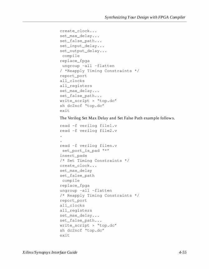
Synthesizing Your Design with FPGA Compiler
create_clock...set_max_delay...set_false_path...set_input_delay...set_output_delay... compilereplace_fpga ungroup –all –flatten/ *Reapply Timing Constraints */report_portall_clocksall_registersset_max_delay...set_false_path...write_script > “top.dc”sh dc2ncf “top.dc”exit
The Verilog Set Max Delay and Set False Path example follows.
read –f verilog file1.vread –f verilog file2.v..read –f verilog filen.v set_port_is_pad “*”insert_pads/* Set Timing Constraints */create_clock...set_max_delayset_false_path compilereplace_fpgaungroup –all –flatten/* Reapply Timing Constraints */report_portall_clocksall_registersset_max_delay...set_false_path...write_script > “top.dc”sh dc2ncf “top.dc”exit
Xilinx/Synopsys Interface Guide 4-55
Xilinx/Synopsys Interface Guide
Set Multicycle Path
DC2NCF does not support translation of the Set Multicycle Path command. However, you can achieve equivalent functionality with the Set Max Delay command. These two constraints differ in the interpretation of their numerical field.
The syntax of the two commands follows.
set_multicycle_path path_multiplier,[–rise | –fall] \
[–setup | –hold] [–start | –end] \
[–from from_list] [–to to_list] [–reset_path] \
set_max_delay delay_value [–rise | –fall] \
[–from from_list] [–to to_list] \
[–group_path group_name] [–reset_path]
Delay_value specifies the absolute delay value in nanoseconds for the path between the indicated start and end points. The period of the clock that controls the path between the indicated start and end points multiplies path_multiplier and specifies the path delay.
You can use the Set Max Delay command instead of the Set Multicycle Path command by using the clock period multiplied by the path_multiplier for the delay_value. The following example illustrates this command substitution.
create_clock my_clock_port –period 50 \
set_multicycle_path 2 –from find(cell,“a_reg”) \
–to find(cell,“b_reg”)
Alternatively, you can express this as shown in the following example.
create_clock my_clock_port –period 50 \
set_max_delay 100 –from find(cell,“a_reg”) \
–to find(cell,“b_reg”)
4-56 Xilinx Development System
Synthesizing Your Design with FPGA Compiler
Note: When DC2NCF translates Synopsys timing commands into Xilinx syntax, point-to-point exception commands (such as Set Max Delay and Set False Path) result in timegroup statements in the resulting NCF file. For identification purposes, the names allocated to timegroups include the line number of the related command in the Synopsys script file. The following example shows the translation of a line of a Synopsys script file.
set_max_delay 57 –from find(clock,clocka)
The DC2NCF output NCF file appears as follows.
TIMEGROUP tg_5_dest = FFS:LATCHES:RAMS:PADS;
ts_01 = FROM:clocka:TO:tg_5_dest:57;
Compiling Your DesignAfter you insert the I/O pads, you can optimize your design for area, speed, or a combination of both. To get the most effective results from FPGA Compiler, apply accurate and achievable constraints. For example, if you set a timing goal of 0 ns on all ports, FPGA Compiler attempts to meet this goal by duplicating logic to reduce critical paths. This can result in a significant and possibly unwarranted increase in CLB and interconnect usage.
The following sections describe the commands you use to compile and optimize your HDL design.
Optimizing Logic Across Hierarchical BoundariesCLBs contain Boolean logic implemented in both function generators and flip-flops. Compiling a hierarchical design or a design that uses a DesignWare module does not optimize the logic across the hierarchical boundary because DesignWare modules exist inside their own hierarchical boundaries. Therefore, some CLBs only implement flip-flops and contain unused function generators and other CLBs only implement function generators and contain unused flip-flops. Additionally, the Boolean logic in one hierarchy is not optimized with that in another to reduce the CLB area or logic levels.
The choice of hierarchical boundaries can have a significant impact on the area and speed of the synthesized design. Using FPGA Compiler, you can optimize a design while preserving these hierarchical boundaries.
Xilinx/Synopsys Interface Guide 4-57
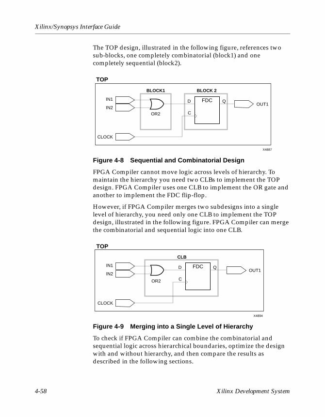
Xilinx/Synopsys Interface Guide
The TOP design, illustrated in the following figure, references two sub-blocks, one completely combinatorial (block1) and one completely sequential (block2).
Figure 4-8 Sequential and Combinatorial Design
FPGA Compiler cannot move logic across levels of hierarchy. To maintain the hierarchy you need two CLBs to implement the TOP design. FPGA Compiler uses one CLB to implement the OR gate and another to implement the FDC flip-flop.
However, if FPGA Compiler merges two subdesigns into a single level of hierarchy, you need only one CLB to implement the TOP design, illustrated in the following figure. FPGA Compiler can merge the combinatorial and sequential logic into one CLB.
Figure 4-9 Merging into a Single Level of Hierarchy
To check if FPGA Compiler can combine the combinatorial and sequential logic across hierarchical boundaries, optimize the design with and without hierarchy, and then compare the results as described in the following sections.
OR2
BLOCK 2BLOCK1
TOP
OUT1IN1
IN2
CLOCK
X4887
D QFDC
C
OR2
CLB
TOP
OUT1IN1
IN2
CLOCK
X4894
D QFDC
C
4-58 Xilinx Development System
Synthesizing Your Design with FPGA Compiler
By default, FPGA Compiler does not flatten your design hierarchy. You must use the Compile command with the Ungroup All option to flatten your design. However, FPGA Compiler only partially optimizes logic across hierarchical modules. Full optimization is possible across those parts of your design hierarchy ungrouped in FPGA Compiler. Flatten or reconstruct hierarchy artificially prior to using the Compile command by issuing the Group and Ungroup commands. Follow the guidelines for controlling flattening in the Synopsys Design Compiler Family Reference Manual.
Using a Flattening Optimization Strategy
Flattening eliminates the existing logic structure. In general, you can flatten random control logic because automatic structuring usually improves upon manual structuring. For FPGA designs, flatten designs when the number of CLBs needed to implement a Boolean function seems too high or there are too many logic levels. You probably do not need to flatten regular or highly structured designs such as adders and ALUs designed with an explicit structure.
Flattening works especially well for the FPGA CLB structure because FPGA Compiler has a built-in optimizer for Boolean logic. This algorithm works efficiently when the structure decomposes sufficiently so that the Boolean logic can map into the CLB function generators.
Compiling the Design with Hierarchy
To compile the design and maintain its hierarchy, enter the following command.
compile –map_effort [low|med|high] \
–boundary_optimization
This command enables some logic optimization to occur across hierarchical boundaries. For more information on this option, refer to the Synopsys Design Compiler Family Reference Manual.
Even a flat design can end up containing hierarchical blocks after compiling. These hierarchical blocks contain either Synopsys DesignWare modules or XDW modules mapped during the optimization process.
Xilinx/Synopsys Interface Guide 4-59
Xilinx/Synopsys Interface Guide
Compiling the Design without Hierarchy
To compile the design without hierarchy, enter the following command.
compile –map_effort [low|med|high] –ungroup_all
This command creates a flattened design and then optimizes it.
If your design contains Synopsys DesignWare modules (after the first compile), re-compile your design using the Ungroup All option. This command does not optimize XDW modules but instead optimizes the entirely combinatorial Synopsys DesignWare modules. You cannot optimize XDW modules because FPGA Compiler interprets them as “black boxes.” The CLBs that implement the XDW parts have unused flip-flops but the Xilinx design implementation tools can correct this later on in the implementation flow.
Using the Ungroup command with the All Flatten option and then compiling differs substantially from invoking the Compile command with the Ungroup All option. If you run the Ungroup command before using the Compile command, DesignWare components inferred during compilation retain their hierarchy and can cause the usage of unnecessary CLBs. See your Synopsys documentation for more information on the Ungroup command.
Compiling a Design with Instantiated I/O CellsThis section describes the design flow if your design contains instantiated I/O cells. If you instantiate all I/O buffers (FPGA Compiler does not need to automatically insert I/O buffers), do not use the Set Port Is Pad and Insert Pads commands. Place a Dont Touch attribute on all instantiated I/O buffers.
If your design contains some instantiated I/O buffers and you want FPGA Complier to automatically insert the rest of the I/O buffers, do the following.
• Use the Set Port Is Pad command only on the I/Os that you want the FPGA Compiler to insert.
• Place a Dont Touch attribute on all instantiated I/O buffers before the design is compiled.
• Issue the Insert Pads command.
4-60 Xilinx Development System
Synthesizing Your Design with FPGA Compiler
See the bidi_reg.vhd and bidi_reg.v examples in the “Inserting Bidirectional I/Os” section for designs that contain both instantiated I/Os and I/Os inserted using FPGA Compiler. The bidi_reg.script (VHDL) in the “Inserting Bidirectional I/Os” section provides an example script file illustrating the correct design flow.
Compiling XC4000, Spartan, and Virtex DesignsThe following sample script file demonstrates how to compile your XC4000 designs using FPGA Compiler.
/* ==================================================*//* Sample Script for Synopsys to Xilinx Using *//* FPGA Compiler *//* Targets the Xilinx XC4028EX-3 and assumes a VHDL *//* source file by way of an example. *//* For general use with XC4000E/EX architectures. *//* Not suitable for use with XC3000A/XC5200 *//* architectures. *//* ==================================================*/
/* ================================================= *//* Set the name of the design’s top-level module. *//* (Makes the script more readable and portable.) *//* Also set some useful variables to record the *//* designer and company name. *//* ================================================= */
TOP = calcMOD1 = clockgenMOD2 = count3MOD3 = statmachMOD4 = stackMOD5 = bardecMOD6 = seg7decMOD7 = aluMOD8 = controlMOD9 = switch7MOD10 = debouncedesigner = “XSI Team”company = “Xilinx, Inc”
Xilinx/Synopsys Interface Guide 4-61
Xilinx/Synopsys Interface Guide
/* ================================================= *//* Analyze and Elaborate the design file and specify *//* the design file format. *//* ================================================= */
analyze –format vhdl MOD1 + “.vhd”analyze –format vhdl MOD2 + “.vhd”analyze –format vhdl MOD3 + “.vhd”analyze –format vhdl MOD4 + “.vhd”analyze –format vhdl MOD5 + “.vhd”analyze –format vhdl MOD6 + “.vhd”analyze –format vhdl MOD7 + “.vhd”analyze –format vhdl MOD8 + “.vhd”analyze –format vhdl MOD9 + “.vhd”analyze –format vhdl MOD10 + “.vhd”analyze –format vhdl TOP + “.vhd”elaborate TOP
/* ================================================= *//* Set the current design to the top level. *//* ================================================= */ current_design TOP
/* ================================================= *//* Set the synthesis design constraints. *//* ================================================= */
remove_constraint –all
/* ================================================= *//* Apply dont_touch attributes to instantiated prims *//* ================================================= */
dont_touch STARTUPBLK dont_touch “OSCILLATOR/OSCILLATOR” dont_touch “OSCILLATOR/CLOCK_BUF”
/* ================================================= *//* Indicate those ports on the top-level module that *//* should become chip-level I/O pads. Assign any I/O *//* attributes or parameters and perform the I/O */
4-62 Xilinx Development System
Synthesizing Your Design with FPGA Compiler
/* synthesis. *//* ================================================= */
set_port_is_pad “*” set_pad_type –slewrate HIGH all_outputs() insert_pads
/* ================================================= *//* Synthesize and optimize the design */ /* ================================================= */
compile –boundary_optimization
/* ================================================= *//* Write the design report files. *//* ================================================= */
report_fpga > TOP + “.fpga” report_timing > TOP + “.timing”
/* ================================================= *//* Write out the design to a DB file. (Post compile) *//* ================================================= */
write –format db –hierarchy –output TOP + “_compiled.db”
/* ================================================= *//* Replace CLBs and IOBs with gates for non-Virtex *//* parts. For Virtex parts do not use replace_fpga *//* ================================================= */
replace_fpga
/* ================================================= *//* Set the part type. *//* ================================================= */
set_attribute TOP “part” –type string “4028expg299-3”
/* ================================================= */
Xilinx/Synopsys Interface Guide 4-63
Xilinx/Synopsys Interface Guide
/* Write out the design to a DB. (Post replace_fpga) *//* ================================================= */
write –format db –hierarchy –output TOP + “.db”
/* ================================================= *//* Flatten the design's hierarchy to rationalize */ /* netlist and constraints files */ /* ================================================= */
ungroup –all –flatten
/* ================================================= *//* Save design in EDIF format as <design>.sedif */ /* ================================================= */
write –format xnf –hierarchy –output TOP + “.edif”
/* ================================================= *//* Write-out the timing constraints that were *//* applied earlier. *//* ================================================= */
write_script > TOP + “.dc”
/* ================================================= *//* Call the Synopsys-to-Xilinx constraints translator*//* utility DC2NCF to convert the Synopsys constraints*//* to a Xilinx NCF file. You may want to view */ /* dc2ncf.log to review the translation process. */ /* ================================================= */
/* sh dc2ncf TOP + “.dc” */
/* ================================================= *//* Exit the Compiler. *//* ================================================= */
exit
4-64 Xilinx Development System
Synthesizing Your Design with FPGA Compiler
/* ================================================= *//* Now run the Xilinx design implementation tools. *//* ================================================= */
Creating the Area ReportFPGA Compiler reports area with the Report FPGA command as follows.
report_fpga
The statistics reported by this command include the number of the following elements used in your design.
• F, G, and H function generators
• XDW cells
• Instantiated cells
• 3-state buffers
• Flip-flops
• IOBs
The Report FPGA command also reports the number of CLBs used for the design on the basis of the mapping performed by FPGA Compiler.
The Report FPGA command provides an accurate CLB count when FPGA Compiler provides packing information to the place and route tools. However, the Synopsys output netlist suppresses packing data. As a result, the actual CLB count can vary between FPGA Compiler’s Report FPGA count and MAP’s mapping report. The Synopsys output netlist suppresses packing data because it impacts the routability of the design. For better results with the Xilinx tools, ensure that the software controls the allocation of flip-flops and function generators to CLBs. You can reactivate the Synopsys packing data.
The reported number of CLBs can vary during design implementation, however, the number of flip-flops, F, G, and H function generators does not. Therefore, you can accurately assess a design’s area in these terms. Use the Synopsys CLB count as a conservative estimate.
Xilinx/Synopsys Interface Guide 4-65
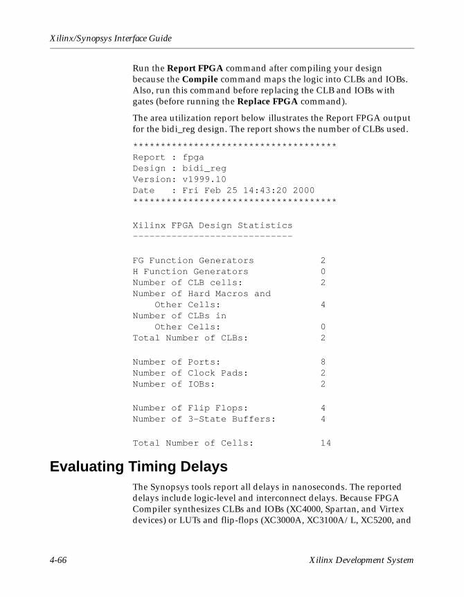
Xilinx/Synopsys Interface Guide
Run the Report FPGA command after compiling your design because the Compile command maps the logic into CLBs and IOBs. Also, run this command before replacing the CLB and IOBs with gates (before running the Replace FPGA command).
The area utilization report below illustrates the Report FPGA output for the bidi_reg design. The report shows the number of CLBs used.
*************************************Report : fpgaDesign : bidi_regVersion: v1999.10Date : Fri Feb 25 14:43:20 2000*************************************
Xilinx FPGA Design Statistics-----------------------------
FG Function Generators 2H Function Generators 0Number of CLB cells: 2Number of Hard Macros and Other Cells: 4Number of CLBs in Other Cells: 0Total Number of CLBs: 2
Number of Ports: 8Number of Clock Pads: 2Number of IOBs: 2
Number of Flip Flops: 4Number of 3-State Buffers: 4
Total Number of Cells: 14
Evaluating Timing DelaysThe Synopsys tools report all delays in nanoseconds. The reported delays include logic-level and interconnect delays. Because FPGA Compiler synthesizes CLBs and IOBs (XC4000, Spartan, and Virtex devices) or LUTs and flip-flops (XC3000A, XC3100A/L, XC5200, and
4-66 Xilinx Development System
Synthesizing Your Design with FPGA Compiler
XC9000 devices), it reports logic-level delays with a higher degree of accuracy than Design Compiler. Because Design Compiler synthesizes only logic gates, it provides only estimates of logic-level delays. Logic-level delays are worst case.
Both FPGA Compiler and Design Compiler estimate possible interconnect delays on the basis of a net’s fanout. These estimates allow you to evaluate your design’s performance prior to performing place and route. FPGA Compiler applies the wire-load model only to nets between CLBs and IOBs (XC4000 devices) or between LUTs, I/Os, and flip-flops (XC3000A, XC3100A/L, and XC5200 devices). Design Compiler’s estimates of interconnect delays based on fanout match FPGA Compiler’s. However, because Design Compiler does not have information on how your design maps and packs into LUTs or CLBs, it applies the wire-load model to every net in your design. This results in a less accurate net contribution to overall path delays. You can use either average or worst-case wire-load models.
To evaluate the timing results, use the Report Timing command.
report_timing
Refer to the Synopsys Design Compiler Family Reference Manual for information on other report options.
Run the Report Timing command after compiling the design because the Compile command maps the logic into CLBs and IOBs, and before running the Replace FPGA command, which replaces the CLBs and IOBs with gates.
Only XC4000 and Spartan designs require the Replace FPGA command.
Synopsys assigns a default “average case” wire-load model to all nets in your design. Refer to the “Setting the Wire-Load Model” section at the beginning of this chapter for more information.
Generating Reports for DebuggingFPGA Compiler includes additional commands that provide CLB and IOB information for debugging purposes.
Use the following commands before using the Replace FPGA command to replace CLBs and IOBs with gates.
Xilinx/Synopsys Interface Guide 4-67
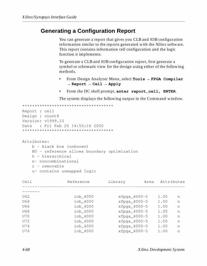
Xilinx/Synopsys Interface Guide
Generating a Configuration ReportYou can generate a report that gives you CLB and IOB configuration information similar to the reports generated with the Xilinx software. This report contains information cell configuration and the logic function it implements.
To generate a CLB and IOB configuration report, first generate a symbol or schematic view for the design using either of the following methods.
• From Design Analyzer Menu, select Tools → FPGA Compiler → Report → Cell → Apply.
• From the DC shell prompt, enter report_cell, ENTER.
The system displays the following output in the Command window.
*************************************Report : cellDesign : count8Version: v1999.10Date : Fri Feb 25 14:55:16 2000*************************************
Attributes: b - black box (unknown) BO - reference allows boundary optimization h - hierarchical n- noncombinational r - removable u- contains unmapped logic
Cell Reference Library Area Attributes-------------------------------------------------------------------------U62 iob_4000 xfpga_4000-5 1.00 nU64 iob_4000 xfpga_4000-5 1.00 nU66 iob_4000 xfpga_4000-5 1.00 nU68 iob_4000 xfpga_4000-5 1.00 nU70 iob_4000 xfpga_4000-5 1.00 nU72 iob_4000 xfpga_4000-5 1.00 nU74 iob_4000 xfpga_4000-5 1.00 nU76 iob_4000 xfpga_4000-5 1.00 n
4-68 Xilinx Development System
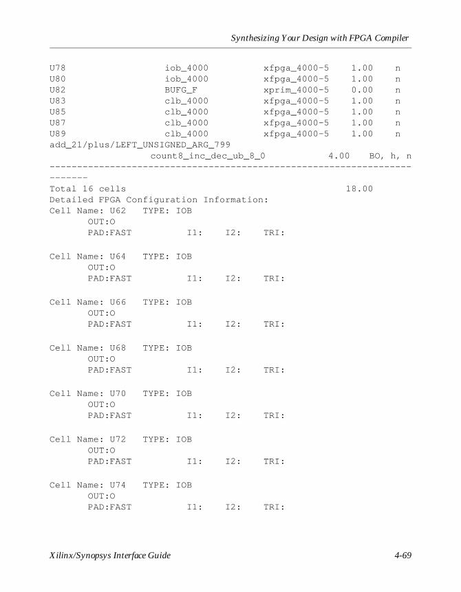
Synthesizing Your Design with FPGA Compiler
U78 iob_4000 xfpga_4000-5 1.00 nU80 iob_4000 xfpga_4000-5 1.00 nU82 BUFG_F xprim_4000-5 0.00 nU83 clb_4000 xfpga_4000-5 1.00 nU85 clb_4000 xfpga_4000-5 1.00 nU87 clb_4000 xfpga_4000-5 1.00 nU89 clb_4000 xfpga_4000-5 1.00 nadd_21/plus/LEFT_UNSIGNED_ARG_799 count8_inc_dec_ub_8_0 4.00 BO, h, n-------------------------------------------------------------------------Total 16 cells 18.00Detailed FPGA Configuration Information:Cell Name: U62 TYPE: IOB OUT:O PAD:FAST I1: I2: TRI:
Cell Name: U64 TYPE: IOB OUT:O PAD:FAST I1: I2: TRI:
Cell Name: U66 TYPE: IOB OUT:O PAD:FAST I1: I2: TRI:
Cell Name: U68 TYPE: IOB OUT:O PAD:FAST I1: I2: TRI:
Cell Name: U70 TYPE: IOB OUT:O PAD:FAST I1: I2: TRI:
Cell Name: U72 TYPE: IOB OUT:O PAD:FAST I1: I2: TRI:
Cell Name: U74 TYPE: IOB OUT:O PAD:FAST I1: I2: TRI:
Xilinx/Synopsys Interface Guide 4-69
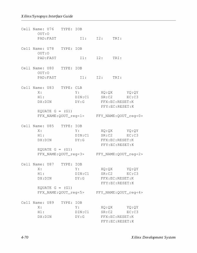
Xilinx/Synopsys Interface Guide
Cell Name: U76 TYPE: IOB OUT:O PAD:FAST I1: I2: TRI:
Cell Name: U78 TYPE: IOB OUT:O PAD:FAST I1: I2: TRI:
Cell Name: U80 TYPE: IOB OUT:O PAD:FAST I1: I2: TRI:
Cell Name: U83 TYPE: CLB X: Y: XQ:QX YQ:QY H1: DIN:C1 SR:C2 EC:C3 DX:DIN DY:G FFX:EC:RESET:K FFY:EC:RESET:K EQUATE G = (G1) FFX_NAME:QOUT_reg<1> FFY_NAME:QOUT_reg<0>
Cell Name: U85 TYPE: IOB X: Y: XQ:QX YQ:QY H1: DIN:C1 SR:C2 EC:C3 DX:DIN DY:G FFX:EC:RESET:K
FFY:EC:RESET:K EQUATE G = (G1) FFX_NAME:QOUT_reg<3> FFY_NAME:QOUT_reg<2>
Cell Name: U87 TYPE: IOB X: Y: XQ:QX YQ:QY H1: DIN:C1 SR:C2 EC:C3 DX:DIN DY:G FFX:EC:RESET:K
FFY:EC:RESET:K EQUATE G = (G1) FFX_NAME:QOUT_reg<5> FFY_NAME:QOUT_reg<4>
Cell Name: U89 TYPE: IOB X: Y: XQ:QX YQ:QY H1: DIN:C1 SR:C2 EC:C3 DX:DIN DY:G FFX:EC:RESET:K
FFY:EC:RESET:K
4-70 Xilinx Development System
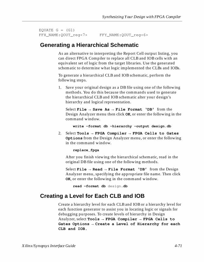
Synthesizing Your Design with FPGA Compiler
EQUATE G = (G1) FFX_NAME:QOUT_reg<7> FFY_NAME:QOUT_reg<6>
Generating a Hierarchical SchematicAs an alternative to interpreting the Report Cell output listing, you can direct FPGA Compiler to replace all CLB and IOB cells with an equivalent set of logic from the target libraries. Use the generated schematic to determine what logic implemented the CLBs and IOBs.
To generate a hierarchical CLB and IOB schematic, perform the following steps.
1. Save your original design as a DB file using one of the following methods. You do this because the commands used to generate the hierarchical CLB and IOB schematic alter your design’s hierarchy and logical representation.
Select File → Save As → File Format ‘DB’ from the Design Analyzer menu then click OK, or enter the following in the command window.
write –format db –hierarchy –output design.db
2. Select Tools → FPGA Compiler → FPGA Cells to Gates Options from the Design Analyzer menu, or enter the following in the command window.
replace_fpga
After you finish viewing the hierarchical schematic, read in the original DB file using one of the following methods.
Select File → Read → File Format ‘DB’ from the Design Analyzer menu, specifying the appropriate file name. Then click OK, or enter the following in the command window.
read –format db design.db
Creating a Level for Each CLB and IOBCreate a hierarchy level for each CLB and IOB or a hierarchy level for each function generator to assist you in locating logic or signals for debugging purposes. To create levels of hierarchy in Design Analyzer, select Tools → FPGA Compiler → FPGA Cells to Gates Options → Create a Level of Hierarchy for each CLB and IOB.
Xilinx/Synopsys Interface Guide 4-71
Xilinx/Synopsys Interface Guide
You can also enter the following at the DC Shell prompt.
replace_fpga –group_cells
After you select these options, the resulting logic does not accurately reflect the timing of the actual CLB and IOB implementation. Timing or area reports then produce inaccurate results.
Generating a Level for Each Function GeneratorGenerate hierarchical schematics that show the logic in each function generator it implements. This process replaces each CLB by an F, G, or H function generator, along with the used flip-flops. The function generators add an additional level of hierarchy. To create a level of hierarchy for each function generator, select Tools → FPGA Compiler → FPGA Cells to Gates Options → Create a Level of Hierarchy for each “Table-lookup” from the Design Analyzer menu.
You can also enter the following at the DC Shell prompt.
replace_fpga –group_tlus
You can now view the implementation of the function generators.
Writing and Saving Your DesignAfter your design meets your timing and area requirements, you can save the design as a DB file. For XC4000, Spartan, and Virtex devices and FPGA Compiler only, replace the CLBs and IOBs with gates. For FPGA Compiler, set the design part type and any other supporting information. Then, write and save your design as a netlist in either XNF (FPGA Compiler non-Virtex architectures) or EDIF (FPGA Compiler and Design Compiler for Virtex architectures) formats.
Saving the DB FileSave the Synopsys database file before converting your design to gates by running the Replace FPGA command (XC4000, Spartan, and FPGA Compiler only). If you use the Replace FPGA command options for debugging, such as Group TLUS and Group Cell, save the DB file before running these debugging options.
To save the DB file, choose one of the following methods.
• Enter the following from the Design Analyzer menu.
4-72 Xilinx Development System
Synthesizing Your Design with FPGA Compiler
File → Save As
File name: design_name.db
File Format: db
Save all Designs in Hierarchy: on
OK
• Type the following at the command line. (Select the top level of your design.)
write –format db –hierarchy –output design_name.db
Replacing CLBs and IOBs with GatesThis section applies to XC4000 and Spartan devices and FPGA Compiler.
After compiling with FPGA Compiler, XC4000 and Spartan designs contain CLB and IOB elements used to determine the best implementation of a design for a given set of constraints. Before writing an output netlist, you must convert these CLBs and IOBs into gates recognizable by the Xilinx software. The mapping information passes to the netlist with the FMAP, HMAP, and, optionally, BLKNM parameters, so you can map your design according to FPGA Compiler’s directions.
Invoking the Replace FPGA Command
Enter the following command at the command line at the top level of your design.
replace_fpga
Replacing CLBs and IOBs in Designs with Hierarchy
Running the Replace FPGA command with either the Group Cells or the Group TLUS option and then writing the netlist file generates netlists for each level of hierarchy in your design. If you use the Group Cells option, each CLB transforms into a level of hierarchy with a netlist created for each CLB. Similarly, if you use the Group TLUS option, each function generator transforms into a level of hierarchy.
If you use these options, perform the following steps.
Xilinx/Synopsys Interface Guide 4-73
Xilinx/Synopsys Interface Guide
1. Delete the design from memory.
2. Read in the saved DB file saved prior to the Replace FPGA command.
3. Run the Replace FPGA command without any options.
Controlling the Synopsys MappingThis section applies only to FPGA Compiler.
By default, the FPGA Compiler XNF Writer contains information on how it should map the logic into the CLB and IOBs. FPGA Compiler uses the FMAP and HMAP symbols to map Boolean logic into F and H function generators, and the BLKNM attribute to group flip-flops and function generators into a CLB.
When the XNF Writer includes FPGA Compiler’s mapping information in the netlist, the accuracy of the estimated timing information increases.
FPGA Compiler provides efficient mapping information, so leave the mapping on. However, using FPGA Compiler to perform mapping decreases the MAP program’s processing time.
Block names can restrict placement and routing. For this reason, FPGA Compiler by default does not write the BLKNM attributes.
The following section describes how to remove FMAP and HMAP information and restore BLKNM attributes.
4-74 Xilinx Development System
Synthesizing Your Design with FPGA Compiler
Removing FMAP and HMAP Symbols
To remove the FMAP and HMAP mapping, enter the following at the command line.
set_attribute find(design,"*") \
"xnfout_write_map_symbols" –type boolean FALSE
Restoring BLKNM Attributes
To restore the creation of BLKNM attributes, enter the following at the command line.
set_attribute find(design,"*") \
"xnfout_use_blknames" –type boolean TRUE
Setting the Design Part TypeType the following command at the command line to select a specific part for the design. The following example uses a 4005EPC84–4 device.
set_attribute design_name "part" \
–type string "4005epc84–4"
You can also specify the part type when running NGDBuild.
Saving the Design Netlist FileFollow the instructions in the appropriate section below to save your design netlist file.
Saving your Netlist in EDIF Format (Design Compiler)
Save your design netlist file in EDIF format with a .sedif extension to denote its source. NGDBuild processes netlists from Synopsys in a slightly different way than other netlists. The .sedif extension indicates to NGDBuild to use the Synopsys design flow.
You can save your design as an SEDIF file by either of the following methods.
Xilinx/Synopsys Interface Guide 4-75
Xilinx/Synopsys Interface Guide
• Select your design and then select the following from the Design Analyzer menu.
File → Save As
File name: design_name.sedif
File Format: edif
Save all Designs in Hierarchy: on
OK
• Enter the following at the command line. (Select the top level of your design.)
write –format edif –hierarchy –output \
design_name.sedif
Saving your Netlist in XNF Format (FPGA Compiler)
Save your design netlist file in XNF format with a .sxnf extension to denote its source. NGDBuild processes netlists from Synopsys in a slightly different way than other netlists. The .sxnf extension indicates to NGDBuild to use the Synopsys design flow.
The XNF netlist format can convey your design’s logical hierarchy only with hierarchical instance names and net names. Therefore, flatten your design’s hierarchy prior to writing out a netlist in XNF format. Although this removes the design hierarchy from the Synopsys design database, hierarchical net and instance names remain unchanged. As a result, the XNF file still conveys your design’s hierarchy. After you have flattened your design, you can then write out the netlist.
You can save your design as an SXNF file by either of the following methods.
• Select your design and then select the following from the Design Analyzer menu.
Setup → Command Window
ungroup –all –flatten
File → Save As
4-76 Xilinx Development System
Synthesizing Your Design with FPGA Compiler
File name: design_name.sxnf
File Format: xnf
Save all Designs in Hierarchy: off
OK
• Enter the following at the command line. (Select the top level of your design.)
ungroup –all –flatten
write –format xnf –output design_name.sxnf
Using the Xilinx Development SystemTo translate your design to a bit file so the Xilinx tools can program your device, perform the following steps.
1. Run NGDBuild on the SXNF or SEDIF file to create an NGD file.
2. Run the MAP program on the NGD file to create a mapped NCD file.
3. Run the TRACE program to determine if PAR will meet your timing goals.
4. Run PAR on the NCD file to place and route your design.
5. Run TRACE again on your placed and routed design.
6. Run NGDAnno on your routed design to create an NGA file.
7. Run either NGD2VHDL or NGD2VER on the NGA file to create a VHD or VER file that can be simulated with the appropriate simulators.
Run the BitGen program to create a bitstream for programming the FPGA.
Xilinx/Synopsys Interface Guide 4-77

Xilinx/Synopsys Interface Guide
4-78 Xilinx Development System
Chapter 5
Using CORE Generator and LogiBLOX
CORE Generator is a graphic user interface (GUI) tool for creating RLOC’d cores. CORE Generator optimizes core layout to the target FPGA architecture, allowing higher performance. CORE Generator differs from LogiBLOX but this information is included here because both provide a GUI toolset you can use to create your design.
Refer to the CORE Generator documentation for more information about using that product with XSI.
LogiBLOX is a GUI tool for creating high-level modules such as counters, shift registers, and multiplexers. LogiBLOX includes both a library of generic modules and a set of tools for customizing them. You can also use the modules you create in your HDL designs. LogiBLOX generates a simulation model (VHDL, EDIF, or Verilog) for each LogiBLOX module during design entry. This enables immediate simulation of LogiBLOX designs without logic implementation.
Refer to the LogiBLOX Guide for a complete explanation of LogiBLOX.
Note LogiBLOX does not support Virtex or its derivatives.
This chapter includes the following sections.
• “Using CORE Generator”
• “Specifying Inputs and Outputs in LogiBLOX”
• “Using LogiBLOX in the HDL Design Flow”
• “Instantiating RAM”
Xilinx/Synopsys Interface guide 5-1
Xilinx/Synopsys Interface guide
Using CORE GeneratorThe basic flow of using CORE Generator with XSI involves selecting a core in CORE Generator, entering parameters, then generating the core. You then instantiate the cores in your XSI design.
The CORE Generatordocumentation provides details about how to use CORE Generatorwith XSI.
Apply a Don’t Touch attribute to all CORE Generator cores used in XSI.
Specifying Inputs and Outputs in LogiBLOXUse the LogiBLOX Module Selector GUI, shown in the following figure, to create LogiBLOX modules. Specifying a LogiBLOX module consists of selecting or deselecting optional pins on the symbol, and specifying various module attributes, resulting in a module customized for a specific function.
5-2 Xilinx Development System
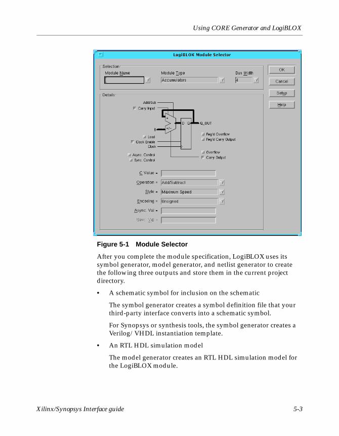
Using CORE Generator and LogiBLOX
Figure 5-1 Module Selector
After you complete the module specification, LogiBLOX uses its symbol generator, model generator, and netlist generator to create the following three outputs and store them in the current project directory.
• A schematic symbol for inclusion on the schematic
The symbol generator creates a symbol definition file that your third-party interface converts into a schematic symbol.
For Synopsys or synthesis tools, the symbol generator creates a Verilog/VHDL instantiation template.
• An RTL HDL simulation model
The model generator creates an RTL HDL simulation model for the LogiBLOX module.
Xilinx/Synopsys Interface guide 5-3
Xilinx/Synopsys Interface guide
The RTL model permits immediate simulation of your design in those environments that support mixed schematic and RTL simulation.
• Gate-level netlists, produced as an alternative simulation medium
The netlist generator creates a gate-level netlist for the LogiBLOX module converted to the third-party’s simulation format. These netlists permit immediate simulation of the design in gate-level simulation environments.
Using LogiBLOX in the HDL Design FlowYou can instantiate LogiBLOX components in your HDL code to take advantage of their high-level functionality.
Express each LogiBLOX module in HDL code with a component declaration describing the module type and a component instantiation describing how the module connects to the other design elements.
Follow these steps to use the LogiBLOX program.
1. Invoke the Module Selector from an icon or from the command line.
2. Configure your project directory using the LogiBLOX Setup window. The default directory is your current directory.
3. Select a base module type (for example, Counter, Memory, or Shift-register)
4. Customize the module by selecting pins and specifying attributes.
5. Press OK after completely specifying a module. Pressing OK initiates the generation of a component instantiation declaration, an RTL model, and an implementation netlist.
6. Deposit the HDL module declaration or instantiation into your HDL design.
7. Complete the signal connections of the instantiated LogiBLOX module to the rest of your HDL design.
5-4 Xilinx Development System
Using CORE Generator and LogiBLOX
8. Conduct functional simulation on your design. The HDL simulator reads the component declaration and looks for an RTL model.
9. Apply a Dont Touch attribute to all LogiBLOX modules.
10. Implement your design by invoking the Xilinx implementation tools.
11. Simulate your post-layout design by converting your design back to a timing netlist and invoking the back-annotation flow.
Instantiating RAMYou can implement memory using LogiBLOX, creating RAM and ROM between 1 to 32 bits wide and 2 to 256 bits deep. Using LogiBLOX to add RAM or ROM to your design provides an efficient implementation of your memory in addition to a simulation model for RTL simulation.
Note: For Verilog designs, use the Remove Design command on instantiated LogiBLOX memory before writing out the design.
You can instantiate RAM in your designs using LogiBLOX, as shown in the following VHDL and Verilog examples. A sample script file follows each example. Refer to the LogiBLOX Guide for more information about using LogiBLOX.
The following example shows how to instantiate RAM using LogiBLOX with VHDL.
library IEEE;use IEEE.std_logic_1164.all;
entity test isport (ADDRESS: IN std_logic_vector(5 downto 0); DATAOUT: OUT std_logic_vector(3 downto 0); DATAIN: IN std_logic_vector(3 downto 0); WRITEN: IN std_logic; CLK: IN std_logic);end test;
architecture inside of test is
component testram
Xilinx/Synopsys Interface guide 5-5
Xilinx/Synopsys Interface guide
port (A: IN std_logic_vector(5 downto 0); DO: OUT std_logic_vector(3 downto 0); DI: IN std_logic_vector(3 downto 0); WR_EN: IN std_logic; WR_CLK: IN std_logic);end component;
begin
U0: testram port map(A=>ADDRESS,DO=>DATAOUT,DI=>DATAIN, WR_EN=>WRITEN,WR_CLK=>CLK);
end inside;
/*===============================================*//* Sample Script for Synopsys to Xilinx Using *//* FPGA Compiler with LogiBLOX Memory *//* Targets the Xilinx XC4028EX-3 and assumes a *//* VHDL source file by way of an example. *//* *//* For general use with XC4000E/EX architectures.*//* Not suitable for use with XC3000A/XC5200 *//* architectures. *//*===============================================*/
/* ============================================= *//* Set the name of the design’s top-level module.*//* (Makes the script more readable and portable.)*//* Also set some useful variables to record the *//* designer and company name. *//* ==============================================*/
TOP = test /* ========================== */ /* Note: Assumes design file- */ /* name and entity name are */ /* the same (minus extension) */ /* ========================== */
designer = "XSI Team" company = "Xilinx, Inc"
5-6 Xilinx Development System
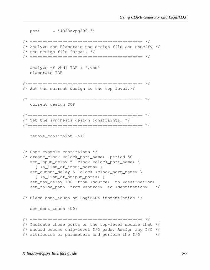
Using CORE Generator and LogiBLOX
part = "4028expg299-3"
/* ============================================= *//* Analyze and Elaborate the design file and specify *//* the design file format. *//* ============================================= */
analyze –f vhdl TOP + ".vhd" elaborate TOP
/*============================================== *//* Set the current design to the top level.*/
/* ============================================= */ current_design TOP
/*============================================== *//* Set the synthesis design constraints. *//*============================================== */
remove_constraint –all
/* Some example constraints *//* create_clock <clock_port_name> –period 50 set_input_delay 5 –clock <clock_port_name> \ { <a_list_of_input_ports> } set_output_delay 5 –clock <clock_port_name> \ { <a_list_of_output_ports> } set_max_delay 100 –from <source> –to <destination> set_false_path –from <source> –to <destination> */
/* Place dont_touch on LogiBLOX instantiation */
set_dont_touch {U0}
/* ============================================= *//* Indicate those ports on the top-level module that */ /* should become chip-level I/O pads. Assign any I/O *//* attributes or parameters and perform the I/O */
Xilinx/Synopsys Interface guide 5-7
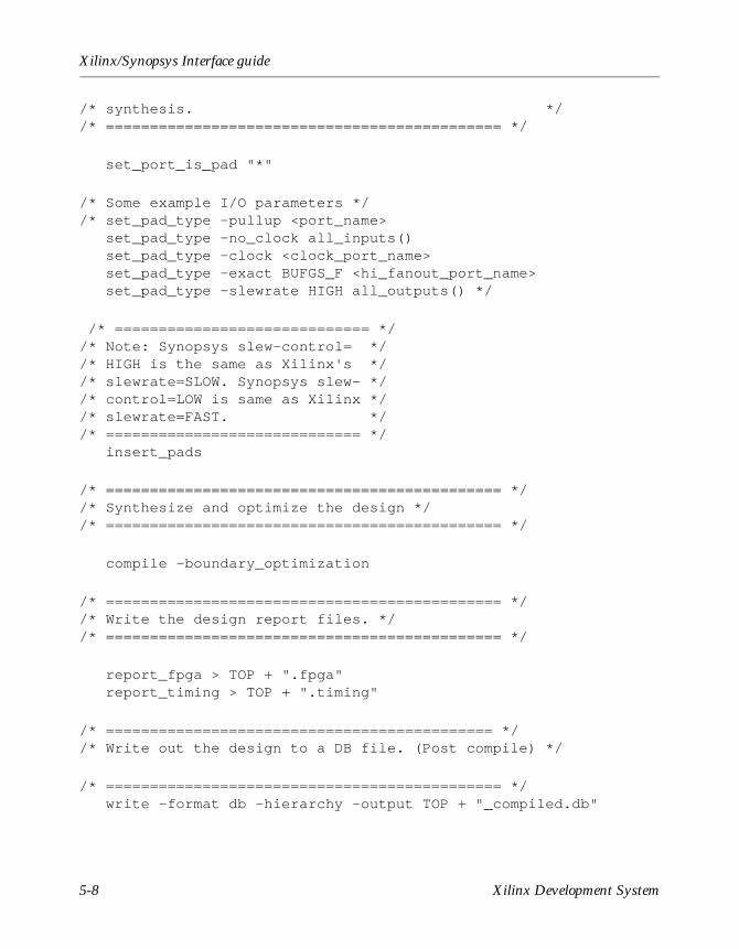
Xilinx/Synopsys Interface guide
/* synthesis. *//* ============================================= */
set_port_is_pad "*"
/* Some example I/O parameters *//* set_pad_type –pullup <port_name> set_pad_type –no_clock all_inputs() set_pad_type –clock <clock_port_name> set_pad_type –exact BUFGS_F <hi_fanout_port_name> set_pad_type –slewrate HIGH all_outputs() */
/* ============================= *//* Note: Synopsys slew-control= *//* HIGH is the same as Xilinx's *//* slewrate=SLOW. Synopsys slew- *//* control=LOW is same as Xilinx *//* slewrate=FAST. *//* ============================= */ insert_pads
/* ============================================= *//* Synthesize and optimize the design *//* ============================================= */
compile –boundary_optimization
/* ============================================= *//* Write the design report files. *//* ============================================= */
report_fpga > TOP + ".fpga" report_timing > TOP + ".timing"
/* ============================================ *//* Write out the design to a DB file. (Post compile) */
/* ============================================= */ write –format db –hierarchy –output TOP + "_compiled.db"
5-8 Xilinx Development System
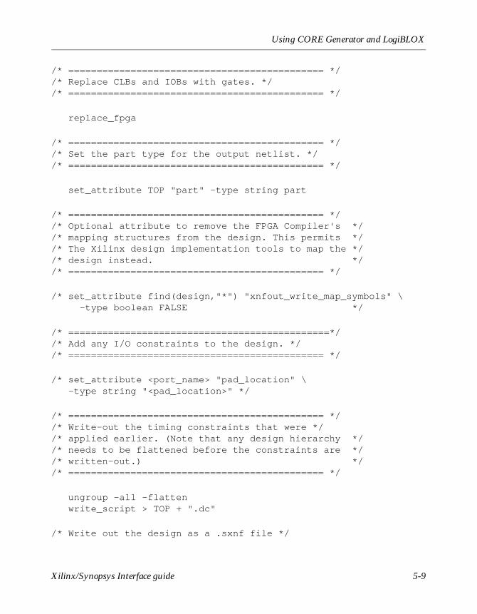
Using CORE Generator and LogiBLOX
/* ============================================= *//* Replace CLBs and IOBs with gates. *//* ============================================= */
replace_fpga
/* ============================================= *//* Set the part type for the output netlist. *//* ============================================= */
set_attribute TOP "part" –type string part
/* ============================================= *//* Optional attribute to remove the FPGA Compiler's *//* mapping structures from the design. This permits *//* The Xilinx design implementation tools to map the *//* design instead. *//* ============================================= */
/* set_attribute find(design,"*") "xnfout_write_map_symbols" \ –type boolean FALSE */
/* ==============================================*//* Add any I/O constraints to the design. *//* ============================================= */
/* set_attribute <port_name> "pad_location" \ –type string "<pad_location>" */
/* ============================================= *//* Write-out the timing constraints that were *//* applied earlier. (Note that any design hierarchy *//* needs to be flattened before the constraints are *//* written-out.) *//* ============================================= */
ungroup –all –flatten write_script > TOP + ".dc"
/* Write out the design as a .sxnf file */
Xilinx/Synopsys Interface guide 5-9
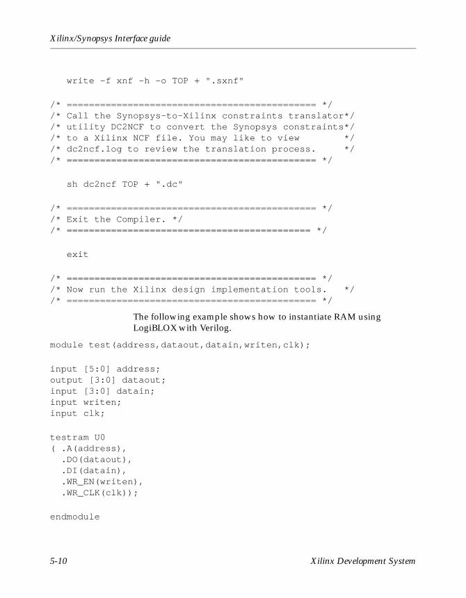
Xilinx/Synopsys Interface guide
write –f xnf –h –o TOP + ".sxnf"
/* ============================================= *//* Call the Synopsys-to-Xilinx constraints translator*//* utility DC2NCF to convert the Synopsys constraints*//* to a Xilinx NCF file. You may like to view *//* dc2ncf.log to review the translation process. *//* ============================================= */
sh dc2ncf TOP + ".dc"
/* ============================================= *//* Exit the Compiler. *//* ============================================ */
exit
/* ============================================= *//* Now run the Xilinx design implementation tools. *//* ============================================= */
The following example shows how to instantiate RAM using LogiBLOX with Verilog.
module test(address,dataout,datain,writen,clk);
input [5:0] address;output [3:0] dataout;input [3:0] datain;input writen;input clk;
testram U0( .A(address), .DO(dataout), .DI(datain), .WR_EN(writen), .WR_CLK(clk));
endmodule
5-10 Xilinx Development System
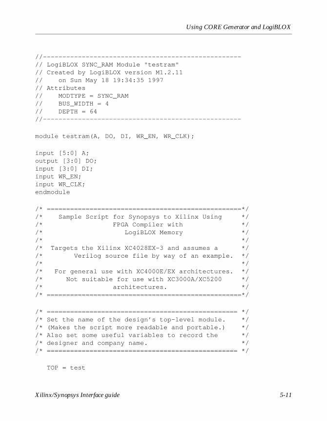
Using CORE Generator and LogiBLOX
//---------------------------------------------------// LogiBLOX SYNC_RAM Module "testram"// Created by LogiBLOX version M1.2.11// on Sun May 18 19:34:35 1997// Attributes // MODTYPE = SYNC_RAM// BUS_WIDTH = 4// DEPTH = 64//---------------------------------------------------
module testram(A, DO, DI, WR_EN, WR_CLK);
input [5:0] A;output [3:0] DO;input [3:0] DI;input WR_EN;input WR_CLK;endmodule
/* ==================================================*//* Sample Script for Synopsys to Xilinx Using *//* FPGA Compiler with *//* LogiBLOX Memory *//* *//* Targets the Xilinx XC4028EX-3 and assumes a *//* Verilog source file by way of an example. *//* *//* For general use with XC4000E/EX architectures. *//* Not suitable for use with XC3000A/XC5200 *//* architectures. *//* ==================================================*/
/* ================================================= *//* Set the name of the design’s top-level module. *//* (Makes the script more readable and portable.) *//* Also set some useful variables to record the *//* designer and company name. *//* ================================================= */
TOP = test
Xilinx/Synopsys Interface guide 5-11
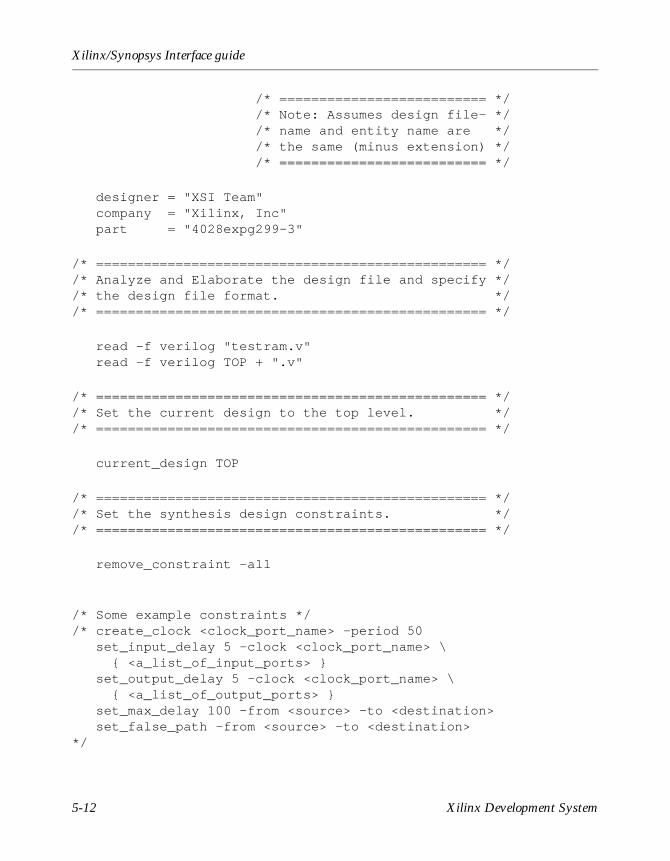
Xilinx/Synopsys Interface guide
/* ========================== */ /* Note: Assumes design file- */ /* name and entity name are */ /* the same (minus extension) */ /* ========================== */
designer = "XSI Team" company = "Xilinx, Inc" part = "4028expg299-3"
/* ================================================= *//* Analyze and Elaborate the design file and specify *//* the design file format. *//* ================================================= */
read –f verilog "testram.v" read –f verilog TOP + ".v"
/* ================================================= *//* Set the current design to the top level. *//* ================================================= */
current_design TOP
/* ================================================= *//* Set the synthesis design constraints. */ /* ================================================= */
remove_constraint –all
/* Some example constraints *//* create_clock <clock_port_name> –period 50 set_input_delay 5 –clock <clock_port_name> \ { <a_list_of_input_ports> } set_output_delay 5 –clock <clock_port_name> \ { <a_list_of_output_ports> } set_max_delay 100 –from <source> –to <destination> set_false_path –from <source> –to <destination>*/
5-12 Xilinx Development System
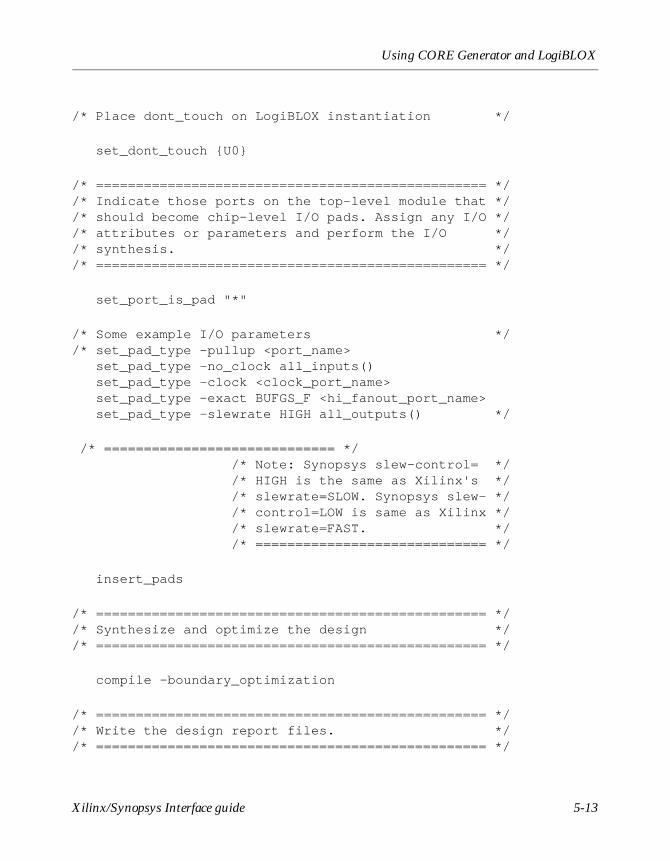
Using CORE Generator and LogiBLOX
/* Place dont_touch on LogiBLOX instantiation */
set_dont_touch {U0}
/* ================================================= *//* Indicate those ports on the top-level module that */ /* should become chip-level I/O pads. Assign any I/O *//* attributes or parameters and perform the I/O *//* synthesis. *//* ================================================= */
set_port_is_pad "*"
/* Some example I/O parameters *//* set_pad_type –pullup <port_name> set_pad_type –no_clock all_inputs() set_pad_type –clock <clock_port_name> set_pad_type –exact BUFGS_F <hi_fanout_port_name> set_pad_type –slewrate HIGH all_outputs() */
/* ============================= */ /* Note: Synopsys slew-control= */ /* HIGH is the same as Xilinx's */ /* slewrate=SLOW. Synopsys slew- */ /* control=LOW is same as Xilinx */ /* slewrate=FAST. */ /* ============================= */
insert_pads
/* ================================================= *//* Synthesize and optimize the design *//* ================================================= */
compile –boundary_optimization
/* ================================================= *//* Write the design report files. *//* ================================================= */
Xilinx/Synopsys Interface guide 5-13
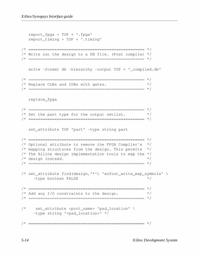
Xilinx/Synopsys Interface guide
report_fpga > TOP + ".fpga" report_timing > TOP + ".timing"
/* ================================================= *//* Write out the design to a DB file. (Post compile) *//* ================================================= */
write –format db –hierarchy –output TOP + "_compiled.db"
/* ================================================= *//* Replace CLBs and IOBs with gates. *//* ================================================= */
replace_fpga
/* ================================================= *//* Set the part type for the output netlist. *//* ================================================= */
set_attribute TOP "part" –type string part
/* ================================================= *//* Optional attribute to remove the FPGA Compiler's *//* mapping structures from the design. This permits *//* The Xilinx design implementation tools to map the *//* design instead. *//* ================================================= */
/* set_attribute find(design,"*") "xnfout_write_map_symbols" \ –type boolean FALSE */
/* ================================================= *//* Add any I/O constraints to the design. *//* ================================================= */
/* set_attribute <port_name> "pad_location" \ –type string "<pad_location>" */
/* ================================================= */
5-14 Xilinx Development System
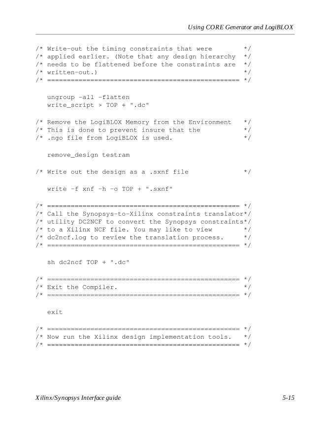
Using CORE Generator and LogiBLOX
/* Write-out the timing constraints that were *//* applied earlier. (Note that any design hierarchy *//* needs to be flattened before the constraints are *//* written-out.) *//* ================================================= */
ungroup –all –flatten write_script > TOP + ".dc"
/* Remove the LogiBLOX Memory from the Environment *//* This is done to prevent insure that the *//* .ngo file from LogiBLOX is used. */
remove_design testram
/* Write out the design as a .sxnf file */
write –f xnf –h –o TOP + ".sxnf"
/* ================================================= *//* Call the Synopsys-to-Xilinx constraints translator*//* utility DC2NCF to convert the Synopsys constraints*//* to a Xilinx NCF file. You may like to view *//* dc2ncf.log to review the translation process. *//* ================================================= */
sh dc2ncf TOP + ".dc"
/* ================================================= *//* Exit the Compiler. *//* ================================================= */
exit
/* ================================================= *//* Now run the Xilinx design implementation tools. *//* ================================================= */
Xilinx/Synopsys Interface guide 5-15
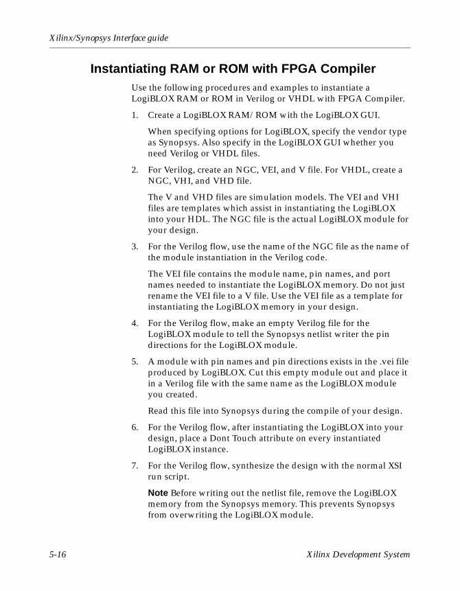
Xilinx/Synopsys Interface guide
Instantiating RAM or ROM with FPGA CompilerUse the following procedures and examples to instantiate a LogiBLOX RAM or ROM in Verilog or VHDL with FPGA Compiler.
1. Create a LogiBLOX RAM/ROM with the LogiBLOX GUI.
When specifying options for LogiBLOX, specify the vendor type as Synopsys. Also specify in the LogiBLOX GUI whether you need Verilog or VHDL files.
2. For Verilog, create an NGC, VEI, and V file. For VHDL, create a NGC, VHI, and VHD file.
The V and VHD files are simulation models. The VEI and VHI files are templates which assist in instantiating the LogiBLOX into your HDL. The NGC file is the actual LogiBLOX module for your design.
3. For the Verilog flow, use the name of the NGC file as the name of the module instantiation in the Verilog code.
The VEI file contains the module name, pin names, and port names needed to instantiate the LogiBLOX memory. Do not just rename the VEI file to a V file. Use the VEI file as a template for instantiating the LogiBLOX memory in your design.
4. For the Verilog flow, make an empty Verilog file for the LogiBLOX module to tell the Synopsys netlist writer the pin directions for the LogiBLOX module.
5. A module with pin names and pin directions exists in the .vei file produced by LogiBLOX. Cut this empty module out and place it in a Verilog file with the same name as the LogiBLOX module you created.
Read this file into Synopsys during the compile of your design.
6. For the Verilog flow, after instantiating the LogiBLOX into your design, place a Dont Touch attribute on every instantiated LogiBLOX instance.
7. For the Verilog flow, synthesize the design with the normal XSI run script.
Note Before writing out the netlist file, remove the LogiBLOX memory from the Synopsys memory. This prevents Synopsys from overwriting the LogiBLOX module.
5-16 Xilinx Development System
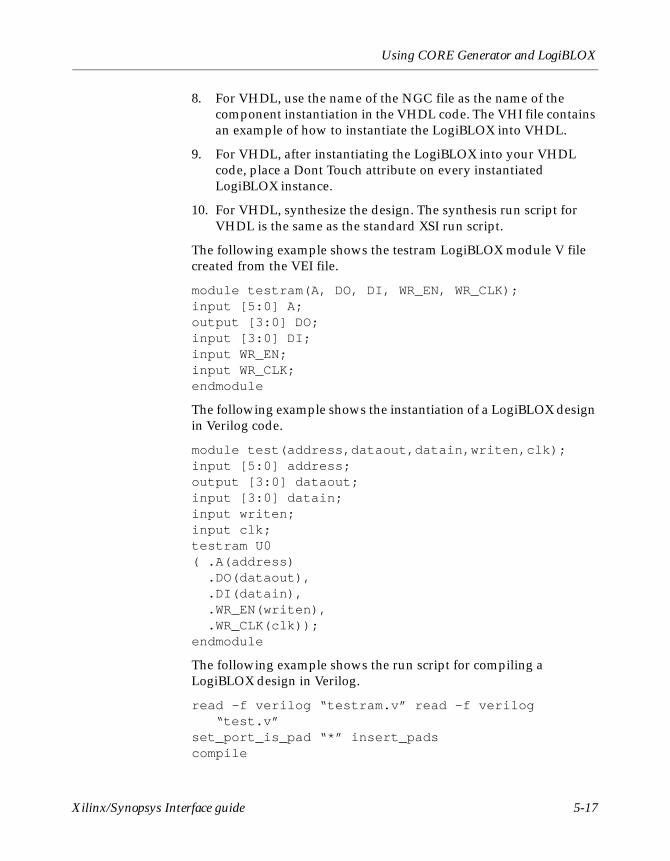
Using CORE Generator and LogiBLOX
8. For VHDL, use the name of the NGC file as the name of the component instantiation in the VHDL code. The VHI file contains an example of how to instantiate the LogiBLOX into VHDL.
9. For VHDL, after instantiating the LogiBLOX into your VHDL code, place a Dont Touch attribute on every instantiated LogiBLOX instance.
10. For VHDL, synthesize the design. The synthesis run script for VHDL is the same as the standard XSI run script.
The following example shows the testram LogiBLOX module V file created from the VEI file.
module testram(A, DO, DI, WR_EN, WR_CLK);input [5:0] A;output [3:0] DO;input [3:0] DI;input WR_EN;input WR_CLK;endmodule
The following example shows the instantiation of a LogiBLOX design in Verilog code.
module test(address,dataout,datain,writen,clk);input [5:0] address;output [3:0] dataout;input [3:0] datain;input writen;input clk;testram U0( .A(address) .DO(dataout), .DI(datain), .WR_EN(writen), .WR_CLK(clk));endmodule
The following example shows the run script for compiling a LogiBLOX design in Verilog.
read -f verilog “testram.v” read -f verilog “test.v”
set_port_is_pad “*” insert_padscompile
Xilinx/Synopsys Interface guide 5-17
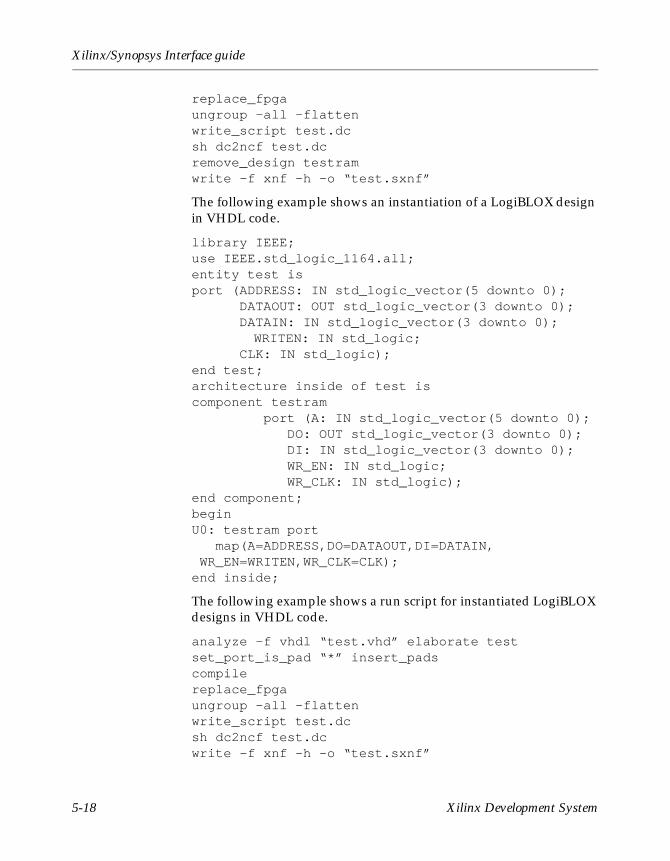
Xilinx/Synopsys Interface guide
replace_fpgaungroup -all -flattenwrite_script test.dcsh dc2ncf test.dcremove_design testramwrite -f xnf -h -o “test.sxnf”
The following example shows an instantiation of a LogiBLOX design in VHDL code.
library IEEE;use IEEE.std_logic_1164.all;entity test isport (ADDRESS: IN std_logic_vector(5 downto 0); DATAOUT: OUT std_logic_vector(3 downto 0); DATAIN: IN std_logic_vector(3 downto 0); WRITEN: IN std_logic;
CLK: IN std_logic);end test;architecture inside of test iscomponent testram port (A: IN std_logic_vector(5 downto 0); DO: OUT std_logic_vector(3 downto 0); DI: IN std_logic_vector(3 downto 0); WR_EN: IN std_logic; WR_CLK: IN std_logic);end component;beginU0: testram port
map(A=ADDRESS,DO=DATAOUT,DI=DATAIN, WR_EN=WRITEN,WR_CLK=CLK);end inside;
The following example shows a run script for instantiated LogiBLOX designs in VHDL code.
analyze -f vhdl “test.vhd” elaborate testset_port_is_pad “*” insert_padscompilereplace_fpgaungroup -all -flattenwrite_script test.dcsh dc2ncf test.dcwrite -f xnf -h -o “test.sxnf”
5-18 Xilinx Development System
Using CORE Generator and LogiBLOX
Instantiating RAM or ROM with FPGA Compiler IIUse the following procedures to instantiate a LogiBLOX RAM or ROM in Verilog or VHDL with FPGA Compiler II.
1. Create a LogiBLOX RAM or ROM with the LogiBLOX GUI.
When specifying options for LogiBLOX, specify the vendor type as Synopsys. Also specify in the LogiBLOX GUI whether you need Verilog or VHDL files.
2. For Verilog, create an NGC, VEI, and V file. For VHDL, create an NGC, VHI, and VHD file.
The V and VHD files are simulation models. The VEI and VHI files are templates which assist in instantiating the LogiBLOX into your HDL. The NGC file is the actual LogiBLOX module for your design.
3. For the Verilog flow, use the name of the NGC file as the name of the module instantiation in the Verilog code.
The VEI file contains the module name, pin names, and port names needed to instantiate the LogiBLOX memory. Do not rename the VEI file to a V file. Use the VEI file as a template for instantiating the LogiBLOX memory in your design.
4. For the Verilog flow, make an empty Verilog file for the LogiBLOX module to tell the Synopsys netlist writer the pin directions for the LogiBLOX module.
Xilinx/Synopsys Interface guide 5-19
Xilinx/Synopsys Interface guide
5. In the VEI file produced by LogiBLOX, there is a module with pin names and pin directions. Cut this empty module out and place it in a Verilog file with the same name as the LogiBLOX module you created.
Read this file into FPGA Compiler II during the compiling of your design.
6. After implementing the design files in FPGA Compiler II, notice in the Warnings window a number of warnings about the instantiated LogiBLOX module. FPGA Compiler II reports that it cannot link to the instantiated design. Also, FPGA Compiler II can report that some of the wires attached to the instantiated LogiBLOX have multiple drivers. Ignore these warnings.
Additionally, after implementing the design, in the modules view in the Edit Constraints view, all instantiated LogiBLOX modules are tagged as UNLINKED, a normal situation. UNLINKED means that FPGA Compiler II cannot find a library cell in its synthesis library that matches, a normal situation because the instantiated LogiBLOX is a black-box.
7. After implementing the design, if the implementation icon contains a “!” mark, optimize (synthesize) the design and write out the netlist file.
8. For VHDL, use the name of the NGC file as the name of the component instantiation in the VHDL code.
The VHI file contains an example of how to instantiate the LogiBLOX into VHDL.
9. After implementing the design files in FPGA Compiler II, notice in the Warnings window a number of warnings about the instantiated LogiBLOX module. FPGA Compiler II reports that it cannot link to the instantiated design. Also, FPGA Compiler II can report that some of the wires attached to the instantiated LogiBLOX have multiple drivers. Ignore these warnings.
Additionally, after implementing the design, in the modules view in the Edit Constraints view, all instantiated LogiBLOX modules are tagged as UNLINKED, a normal situation. UNLINKED means that FPGA Compiler II cannot find a library cell in its synthesis library that matches, a normal situation because the instantiated LogiBLOX is a black-box.
5-20 Xilinx Development System
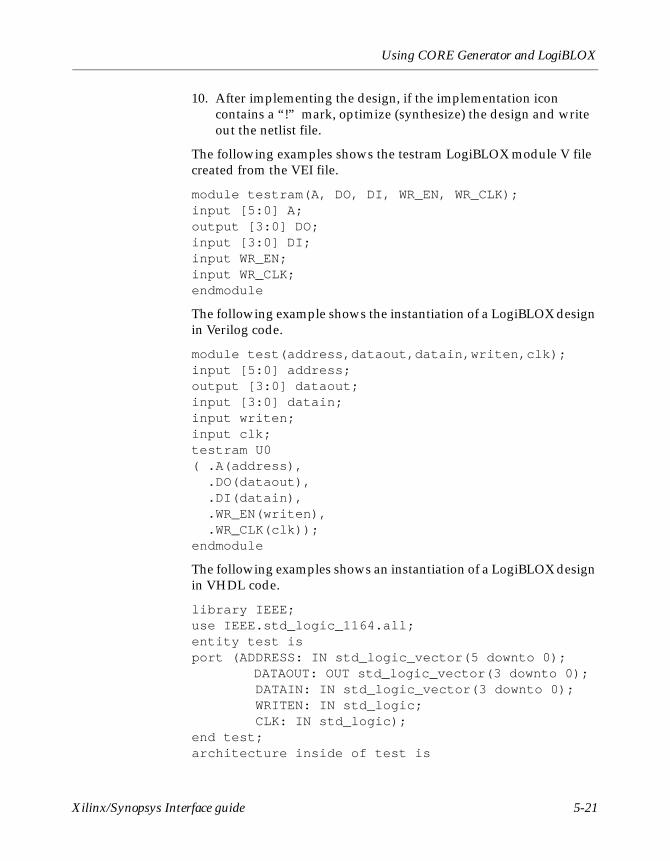
Using CORE Generator and LogiBLOX
10. After implementing the design, if the implementation icon contains a “!” mark, optimize (synthesize) the design and write out the netlist file.
The following examples shows the testram LogiBLOX module V file created from the VEI file.
module testram(A, DO, DI, WR_EN, WR_CLK);input [5:0] A;output [3:0] DO;input [3:0] DI;input WR_EN;input WR_CLK;endmodule
The following example shows the instantiation of a LogiBLOX design in Verilog code.
module test(address,dataout,datain,writen,clk);input [5:0] address;output [3:0] dataout;input [3:0] datain;input writen;input clk;testram U0( .A(address), .DO(dataout), .DI(datain), .WR_EN(writen), .WR_CLK(clk));endmodule
The following examples shows an instantiation of a LogiBLOX design in VHDL code.
library IEEE;use IEEE.std_logic_1164.all;entity test isport (ADDRESS: IN std_logic_vector(5 downto 0); DATAOUT: OUT std_logic_vector(3 downto 0);
DATAIN: IN std_logic_vector(3 downto 0); WRITEN: IN std_logic; CLK: IN std_logic);end test;architecture inside of test is
Xilinx/Synopsys Interface guide 5-21
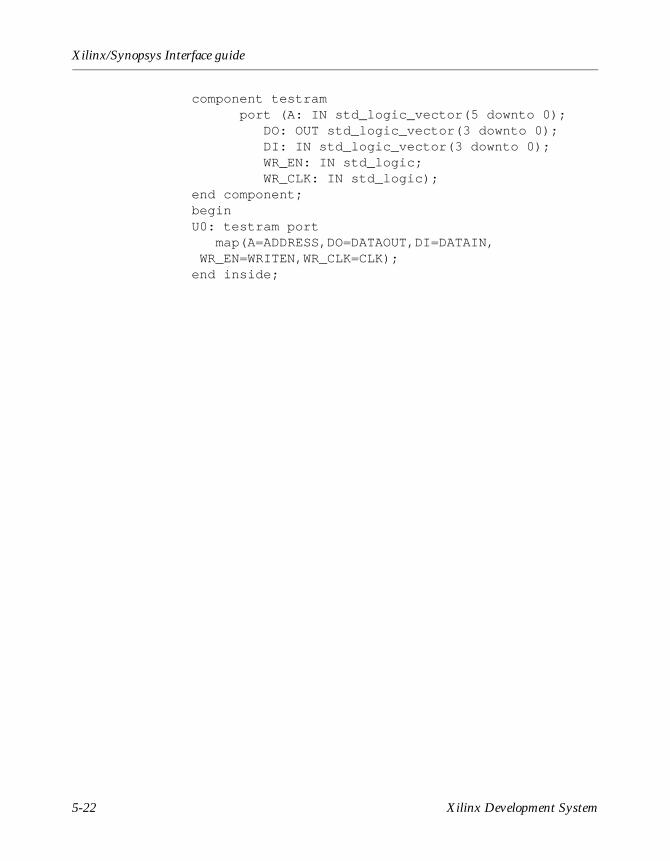
Xilinx/Synopsys Interface guide
component testram port (A: IN std_logic_vector(5 downto 0); DO: OUT std_logic_vector(3 downto 0); DI: IN std_logic_vector(3 downto 0); WR_EN: IN std_logic; WR_CLK: IN std_logic);end component;beginU0: testram port
map(A=ADDRESS,DO=DATAOUT,DI=DATAIN, WR_EN=WRITEN,WR_CLK=CLK);end inside;
5-22 Xilinx Development System
Chapter 6
Simulating Your Design
You can efficiently verifyyour design changes with the XSI VHDL and Verilog simulation options described in this chapter. VHDL simulation supports the VHDL Initiative Towards ASIC Libraries (VITAL) standard, which allows you to simulate with any VITAL-compliant simulator, including Synopsys VSS. Built-in Verilog support allows you to simulate with Cadence Verilog-XL and other compatible simulators.
XSI simulation options provide the following.
• Fast, timing-accurate, gate-level HDL simulation with the VHDL, VITAL-compliant, or Verilog versions of the SimPrim Library
• RTL or post-synthesis, functional verification of designs containing instantiated Xilinx Unified Library components, using either the VITAL or Verilog versions of the UniSim Library
• Support for FPGA architecture features such as Global Set/Reset, Oscillator, RAM, and ROM
This chapter includes the following sections:
• “Simulation Design Flow Overview”
• “Using Simulation Libraries”
• “Working with the VITAL Standard”
• “VHDL and Verilog Simulation Flow”
• “Synthesizing/Simulating for VHDL Global Set/Reset Emulation”
• “NGDBuild Support of Multiple Device Architectures”
• “Recommended VSS Simulation Strategy”
• “VSS Simulation Flow”
Xilinx/Synopsys Interface Guide 6-1
Xilinx/Synopsys Interface Guide
• “Editing the VSS Setup File”
• “Creating a Testbench File”
• “Using RTL Simulation”
• “Implementing Your Design”
Simulation Design Flow OverviewA typical single chip VHDL or Verilog simulation design flow includes the following steps, illustrated in Figure 6-1
1. Generation of a VHDL RTL description
2. VHDL RTL simulation
3. Synthesis implementation
4. Optional unit delay gate-level functional simulation
5. Xilinx Implementation
6. Timing simulation
6-2 Xilinx Development System
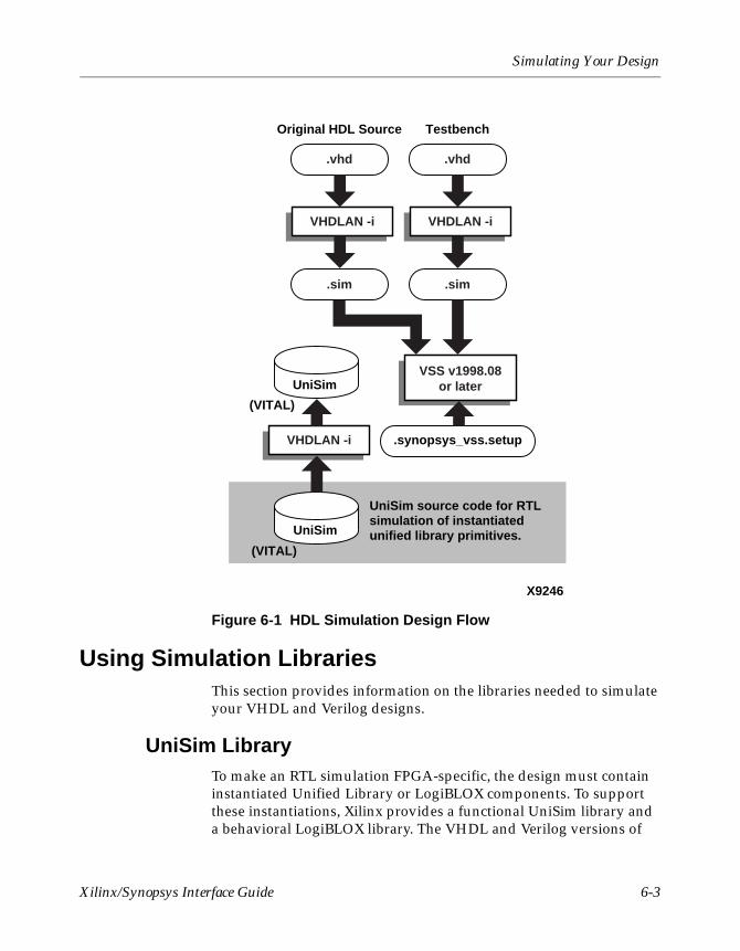
Simulating Your Design
Figure 6-1 HDL Simulation Design Flow
Using Simulation LibrariesThis section provides information on the libraries needed to simulate your VHDL and Verilog designs.
UniSim LibraryTo make an RTL simulation FPGA-specific, the design must contain instantiated Unified Library or LogiBLOX components. To support these instantiations, Xilinx provides a functional UniSim library and a behavioral LogiBLOX library. The VHDL and Verilog versions of
X9246
UniSim
(VITAL)
(VITAL)
Original HDL Source Testbench
UniSim source code for RTL simulation of instantiated unified library primitives.
.synopsys_vss.setup
VSS v1998.08or later
.sim .sim
VHDLAN -i VHDLAN -i
.vhd .vhd
VHDLAN -i
UniSim
Xilinx/Synopsys Interface Guide 6-3
Xilinx/Synopsys Interface Guide
the UniSim library differ because of variations in language features and methodologies. You can also use the UniSim library for post-synthesis, gate-level simulation as discussed in the “VHDL and Verilog Simulation Flow” section.
UniSim Library Structure
Use the UniSim Library for functional simulation only; it contains default unit delays. Structures differ for the library directories for VHDL and Verilog. Only one VHDL library exists for all Xilinx technologies. However, some components contain configuration statements to select the appropriate functionality for a specific architecture. A single library makes it easier to switch between technologies. Because Verilog does not have configuration statements, separate libraries are provided for each technology.
The UniSim Library contains all the Xilinx Unified Library components inferred by most synthesis tools. In addition, the UniSim Library contains commonly instantiated components such as IOs and memory components. Use your synthesis tool’s module generators or LogiBLOX to generate higher order functions such as adders, counters, and RAM.
Schematic macros are not provided because schematic vendors usually provide the lower-level netlist when a synthesis tool imports a design. This lower-level netlist for a schematic macro is required for implementation as well.
Compile the VHDL library using the Xilinx-supplied source files in $XILINX/vhdl/src/unisims. Compile the source files into a library named UNISIM.
6-4 Xilinx Development System
Simulating Your Design
You need to compile the Verilog library only if your Verilog simu-lator supports compiled simulation. Some Xilinx device families, (for example, XC3000), have some library components with a slightly different functionality than the same library components of other Xilinx device families. Separate libraries are provided for those device families. The Verilog libraries located in $XILINX/verilog/src/unisims are in upper case. If needed, you can find the lower case versions of these libraries in the Xilinx Cadence Interface located in $XILINX/cadence/data.
A few differences exist between the upper and lower case versions of the Verilog UniSim libraries. For example, because buf, pullup, and pulldown are reserved words in Verilog, the lower case version of the UniSim library uses buff, pullup1, and pulldown1, and the upper case version uses BUF, PULLUP, and PULDOWN.
UniSim Library Files
You can compile the UniSim VHDL Library to any physical location on your system. You can find the VHDL source files in $XILINX/vhdl/src/unisims, listed below in the order in which you must compile them with the Synopsys VSS compiler.
1. unisim_VCOMP.vhd (component declaration file)
2. unisim_VCOMP52K.vhd (substitutional component declaration file for XC5200 designs)
3. unisim_VPKG.vhd (package file)
4. unisim_VITAL.vhd (model file)
5. unisim_VITAL52K.vhd (additional model file for XC5200 designs)
6. unisim_VCFG4K.vhd (configuration file for XC4000 edge decoders)
7. unisim_VCFG52K.vhd (configuration file for XC5200 internal decoders)
Xilinx/Synopsys Interface Guide 6-5
Xilinx/Synopsys Interface Guide
You can find the uppercase Verilog components in individual component files in the following directories.
• $XILINX/verilog/src/uni3000 (Series 3000)
• $XILINX/verilog/src/uni5200 (Series 5200)
• $XILINX/verilog/src/uni9000 (Series 9000)
• $XILINX/verilog/src/unisims (All other devices)
UniSim Library Component Instantiation
You must refer to the compiled UniSim Library in your VHDL code to instantiate components from this library in your design for RTL simulation. The VHDL simulation tool must map the logical library to the physical location of the compiled library. Verilog must also map to the UniSim Verilog library. Even though VHDL component declarations are provided in the library, component declarations are required in the RTL code for synthesis.
SimPrim LibraryUse the SimPrim (simulation primitive) library for post-NGDBuild, post-map partial timing, and full timing back-annotated simulation.
LogiBLOX LibraryUse the LogiBLOX module generator to create schematic-based modules such as adders, counters, and large memory blocks. For your HDL designs, use LogiBLOX to generate large blocks of memory for instantiation. Refer to the “Using CORE Generator and LogiBLOX” chapter and LogiBLOX Guide for more information.
LogiBLOX Library Compilation
You can compile the LogiBLOX VHDL library to any physical location. You can find the VHDL source files in $XILINX/vhdl/src/logiblox, listed below in the order in which you must compile them.
1. mvlutil.vhd
2. mvlarith.vhd
3. logiblox.vhd
6-6 Xilinx Development System
Simulating Your Design
LogiBLOX Library Component Instantiation
Simulate LogiBLOX components with behavioral code not intended for synthesis. The synthesizer processes the component as a “black box.” The implementation software reads the NGO file created by LogiBLOX. You can find the source libraries for LogiBLOX in $XILINX/vhdl/src/logiblox. The LogiBLOX tool creates the actual models. You must compile the package files into a library called LOGIBLOX. You should compile the LogiBLOX component model in your working directory with your design.
Working with the VITAL StandardVITAL was created to promote the standardization of VHDL libraries and simulators from different vendors. VITAL also defines a standard for back-annotation of timing information to VHDL simulators.
The IEEE-STD 1076.4 VITAL standard accelerates gate-level simulations. Check with your simulator company to verify they support this standard. Also, make sure you use the proper settings and VHDL packages for this standard.
Your simulator can also accelerate IEEE-1164, the standard logic package for Types. VITAL libraries require overhead for timing checks and back-annotation styles. The UniSim Library turns off these timing checks because they do not apply to unit delay functional simulation. The SimPrim back-annotation library by default turns on these timing checks. However, you can turn them off by editing and recompiling the SimPrim components file.
VHDL and Verilog Simulation FlowHDL simulation can occur at five different steps in the design flow, as listed below. Subsequent sections describe each step in more detail.
The following figure illustrates the design flow.
• Register Transfer Level (RTL)
• Post-synthesis, pre-NGDBuild
• Post-NGDBuild, pre-MAP
• Post-MAP partial timing (CLB and IOB block delays only; no net delays)
Xilinx/Synopsys Interface Guide 6-7
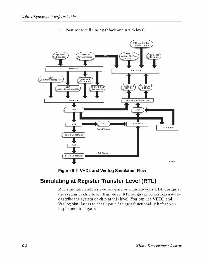
Xilinx/Synopsys Interface Guide
• Post-route full timing (block and net delays)
Figure 6-2 VHDL and Verilog Simulation Flow
Simulating at Register Transfer Level (RTL)RTL simulation allows you to verify or simulate your HDL design at the system or chip level. High-level RTL language constructs usually describe the system or chip at this level. You can use VHDL and Verilog simulators to check your design’s functionality before you implement it in gates.
X9379
VHDL orVerilog SimPrim
Library
VHDL orVerilog Designs
NGD
NGDAnnoNGM
PAR
Simulation
EDIF 2 0 0 &Constraints
UCFUser Constraints File XNF and
Constraints
NCFNetlist Constraint File
NGA
SynthesisLibraries
TestbenchStimulus
NCD & Constraints
NCD & Constraints
NGDBuild
MAP
RTL
CPLD FitterPartial Timing
Full Timing
VHDL or VerilogUniSim Library
Synthesis
Verilog andSDF 2.1
VHDL andSDF 2.1
Netlist Translation Out
6-8 Xilinx Development System
Simulating Your Design
Use a testbench to model the environment of the system or chip. At this level, you can use the UniSim library to instantiate components from the Xilinx Unified Library. You can also instantiate LogiBLOX components if you do not want to use modules generated by your synthesis tool.
Conducting a Post-Synthesis (pre-NGDBuild) Gate-Level Functional Simulation
After synthesizing the system or chip to gates, re-use the testbench in post-synthesis, gate-level functional simulation to simulate the synthesized result. Check consistency with your original design description. In the Xilinx design flow, post-synthesis, gate-level simulation includes any simulation performed after any of the synthesis, map, or place and route steps.
A post-synthesis, pre-NGDBuild gate-level functional simulation allows you to directly verify your design after synthesis. Any differences in the behavior of the original RTL description and the synthesized design can indicate a problem with your synthesis tool. Not all synthesis tools support post-synthesis simulation. The synthesis tool must be able to write VHDL or Verilog output in terms of the UniSim library.
LogiBLOX components remain behavioral models, expanded and represented as gates. The library usage guidelines for RTL simulation also apply to post-synthesis gate-level functional simulation.
Conducting a Post-NGDBuild (Pre-Map) Gate-Level Functional Simulation
If your synthesis tool cannot write UniSim-compatible VHDL or Verilog netlists, you cannot simulate the synthesis output. In this case, use post-NGDBuild (pre-MAP) gate-level functional simulation with generic SimPrim library models. As with the post-synthesis, pre-NGDBuild simulation, this type of gate-level simulation allows you to verify that your design synthesized correctly.
Xilinx/Synopsys Interface Guide 6-9
Xilinx/Synopsys Interface Guide
Conducting a Post-Route Full Timing (Block and Net Delays) Simulation
After using PAR to route your design, you can simulate it with the actual block and net timing delays with the same testbench used in the earlier behavioral simulation. The back-annotation process produces a netlist of SimPrims annotated with the appropriate block and net delay data from the place and route process.
Different simulation libraries are required to support simulation before and after you run NGDBuild on your design. Prior to NGDBuild, designs are expressed as netlists containing Unified Library components. After NGDBuild, designs are expressed as netlists containing SimPrims. While the impact of these library changes are not apparent, designs need different simulation libraries for pre- and post-implementation simulation. Additionally, pre- and post-implementation netlists include different gate-level components.
Synthesizing/Simulating for VHDL Global Set/Reset Emulation
VHDL requires a testbench to control all signal ports. You can instantiate certain VHDL-specific components, explained in the following sections, in the RTL and post-synthesis VHDL description to allow the simulation of the global signals for global set/reset and global 3-state.
NGD2VHDL creates a port in your back-annotated design entity for stimulating the global set/reset or 3-state enable signals. This port does not actually exist on the configured part.
When running NGD2VHDL, you do not need to use the –gp switch to create an external port if you instantiated a STARTUP block in your RTL design. The port is already identified and connected to the global set/reset or 3-state enable signal. If you do not use the –gp switchor did not instantiate a STARTUP block, you must use special components, as described in the following sections.
Note Xilinx recommends that you do not use GSR to reset user Flip-flops on Virtex/Spartan-II
6-10 Xilinx Development System
Simulating Your Design
Using STARTBUF in VHDLSTARTBUF replaces STARTUP. With STARTBUF, you can functionally simulate the GSR/GR net in both functional and timing simulation. By connecting the input pin of the STARTBUF to a top-level port and using STARTBUF as the source for all asynchronous set/reset signals in a design, the Xilinx software can automatically optimize the design to use the GSR/GR in a device. Also, unlike STARTUP, when you instantiate STARTBUF in your design, you can perform functional simulation of the GSR/GR net.
The STARTBUF component passes a reset or 3-state signal in the same way that a buffer allows simulation to proceed and also instantiates the STARTUP block for implementation. One version of STARTBUF works for all devices, however, the XC5200 and the XC4000 STARTUP blocks have different pin names. Implementation with the correct STARTUP block occurs automatically. The following shows an instantiation example of the STARTBUF component.
U1: STARTBUF port map (GSRIN => DEV_GSR_PORT, GTSIN =>DEV_GTS_PORT, CLKIN => ‘0’, GSROUT => GSR_NET, GTSOUT => GTS_NET, Q2OUT => open, Q3OUT => open, Q1Q4OUT => open, DONEINOUT => open):
You can use one or both of the input ports (GSRIN and GTSIN) of the STARTBUF component and the associated output ports (GSROUT and GTSOUT). You can use pins left “open” to pass configuration instructions to the implementation tools by connecting the appropriate signal to the port instead of leaving it open.
Instantiating a STARTUP Block in VHDLThe STARTUP block is traditionally instantiated to identify the GR, PRLD, or GSR signals for implementation. However, simulation can occur only when the net attached to the GSR or GTS goes off the chip because the STARTUP block does not have a simulation model. You can use the new components described below to simulate global set/reset or 3-state nets whether or not the signal goes off the chip.
Xilinx/Synopsys Interface Guide 6-11
Xilinx/Synopsys Interface Guide
Generating a Reset-On-Configuration in VHDLThe Reset-On-Configuration (ROC) component generates a reset pulse during back-annotation if you do not use the –gp option or STARTUP block options. Therefore, you can instantiate the ROC in the front end to match for functionality with GSR, GR, or PRLD (done in both functional and timing simulation). During back-annotation, the entity and architecture for the ROC component are placed in your design’s output VHDL file.
In the front end, the entity and architecture reside in the UniSim Library, and require a component declaration and instantiation.
The ROC component generates a one-time initial pulse to drive the GR, GSR, or PRLD net starting at time “0” for a user-defined pulse width. You can set the pulse width with a generic in a configuration statement. The default value of the generic “width” is 0 ns, which disables the ROC component and holds the global set/reset net low.
The ROC component allows you to simulate with the same testbench as in RTL simulation, and also allows you to control the width of the GSR signal in your implemented design.
One of the easiest methods for mapping the generic involves configuring your testbench. An example testbench configuration for setting the generic follows.
CONFIGURATION cfg_my_timing_testbench OF my_testbench IS FOR my_testbench_architecture FOR ALL:my_design USE ENTITY work.my_design(structure); FOR structure FOR ALL:roc ENTITY work.roc (roc_v); GENERIC MAP (width => 100 ms) END FOR; END FOR; END FOR; END FOR;END cfg_my_timing_testbench;
The following shows an instantiation example of the ROC component.
U1: ROC port map (O => GSR_NET);
6-12 Xilinx Development System
Simulating Your Design
Using ROCBUF in VHDLThe ROCBUF component allows you to provide a stimulus for the ROC signal through a testbench. However, the port connected to it does not implement as a chip pin. Use the –gp switch with NGD2VHDL to use the port in timing simulation. The following example shows an instantiation of the ROCBUF component.
U1: ROCBUF port map (I => SIM_GSR_PORT, O => GSR_NET);
Generating a 3-State-On-Configuration in VHDLThe 3-State-On-Configuration (TOC) component generates a pulse on the design’s 3-state net if you do not use the –tp option or STARTUP block options. The entity and architecture for the TOC component are placed in your design’s output VHDL file.
The TOC component generates a one-time initial pulse to drive the design’s 3-state net starting at time ‘0’ for a user-defined pulse width. You can set the pulse width with a generic in a configuration statement. The default value of “width,” 0 ns, disables the TOC component and causes the 3-state enable to be held low.
The TOC component allows you to simulate with the same testbench as in the RTL simulation, and also allows you to control the width of the 3-state enable signal in your implemented design.
The TOC components require a value for the generic width, usually specified with a configuration statement. Otherwise, you must include a generic map as part of the component instantiation. You can set the generic width with any generic mapping method. Set the “width” generic after consulting The Programmable Logic Data Book for the particular part and mode you have implemented. For example, a XC4000E part can vary from 10 ms to 130 ms. Use the TPOR (Power-On Reset) parameter found in the Configuration Switching Characteristics tables for Master, Slave, and Peripheral modes.
One of the easiest methods for mapping the generic is to configure your testbench. An example testbench configuration for setting the generic follows.
Xilinx/Synopsys Interface Guide 6-13
Xilinx/Synopsys Interface Guide
CONFIGURATION cfg_my_timing_testbench OF my_testbench IS FOR my_testbench_architecture FOR ALL:my_design USE ENTITY work.my_design(structrue); FOR structure FOR ALL:toc ENTITY work.toc (toc_v); GENERIC MAP (width => 100 ms) END FOR; END FOR; END FOR; END FOR;END cfg_my_timing_testbench;
The following example shows an instantiation of the TOC component.
U2: TOC port map (O => GTS_NET);
Using TOCBUF in VHDLThe TOCBUF allows you to provide a stimulus for the global 3-state signal (GTS) through a testbench. However, the port connected to it does not implement as a chip pin. Use the –tp switch with NGD2VHDL to use the port in timing simulation. The following example shows an instantiation of the TOCBUF component.
U2: TOCBUF port map (I =>SIM_GTS_PORT, O =>GTS_NET);
Using Oscillators in VHDLThe SimPrim library does not include a generic oscillator component because the oscillator components in the UNISIM library are device dependent. After back-annotation, your VHDL design output contains the oscillator entity and architectures. The UniSim Library instantiates and simulates oscillators for functional simulation. You must set the period of the base frequency for simulation because the default period of 0 ns disables the oscillator. The oscillator’s frequency can vary significantly with process and temperature.
Before setting the base period parameter, consult The Programmable Logic Data Book for the part you are using. For example, for a XC4000 on-chip oscillator, the base frequency ranges from 4 MHz to 10 MHz, and is nominally 8 MHz. Therefore, the base period generic “period_8m” for the XC4000E OSC4 VHDL model ranges from 250 ns to 100ns, as shown in the following example.
6-14 Xilinx Development System
Simulating Your Design
CONFIGURATION cfg_my_functional_testbench OF my_testbench IS FOR my_testbench_architecture FOR ALL: my_design USE ENTITY work.my_design (my_design_rtl); FOR my_design_rtl FOR ALL:my_submodule USE ENTITY work.my_submodule
(my_submodule_rtl); FOR my_submodule_rtl FOR all: osc4 USE ENTITY work.osc4 (structure) GENERIC MAP (period_8m => 125 nS); END FOR; END FOR; END FOR; END FOR; END FOR; END FOR;END cfg_my_functional_testbench;
Using Global Set/Reset Emulation in VerilogFor more information, refer to the Xilinx/Concept-HDL Interface Guide.
Using Global 3-State Emulation in VerilogFor more information, refer to the Xilinx/Concept-HDL Interface Guide.
Using Oscillators in VerilogFor more information, refer to the Xilinx/Concept-HDL Interface Guide.
NGDBuild Support of Multiple Device ArchitecturesNote Refer to Figure 6-2
NGDBuild processes multiple device architectures with the same core map and place and route software. NGDBuild performs two functions during design implementation.
• NGDBuild stores your design’s elements in a single database so that subsequent operations, such as mapping and routing, are performed on the entire design.
• NGDBuild creates an native generic database (NGD) netlist, which consists of technology-independent primitives common to all FPGAs (SimPrims).
Xilinx/Synopsys Interface Guide 6-15
Xilinx/Synopsys Interface Guide
The MAP program reads this NGD file and creates a native circuit description (NCD) file, a physical description of your design in terms of the target device.
Next, the PAR program places and routes the NCD file. NGDAnno creates an NGA file, a back-annotated NGD file.
Recommended VSS Simulation StrategyBecause of the flexibility of the simulation environment, you can verify your design using various methods. The following steps, explained in subsequent sections, show you one recommended flow for FPGA simulation.
1. Create a .synopsys_vss.setup file.
Before you can begin simulation, you must create a simulation setup file.
2. Specify the initial states of your registers in your VHDL source file.
If you use attributes at the DC Shell command line or in Design Analyzer to control the initial states of the registers in your design, RTL simulation does not reflect those initial states.
3. Create a test bench file.
By following the guidelines described in this section, you can use the same test bench for both RTL and timing simulation.
4. Perform RTL simulation.
This step allows you to debug the behavior of your source design before implementing it in an FPGA.
5. Implement the design in an FPGA.
This step provides the necessary physical resource information necessary for timing simulation.
6. Prepare the timing model.
The NGD2VHDL program prepares a back-annotated timing model of your design for simulation.
7. Perform timing simulation.
6-16 Xilinx Development System
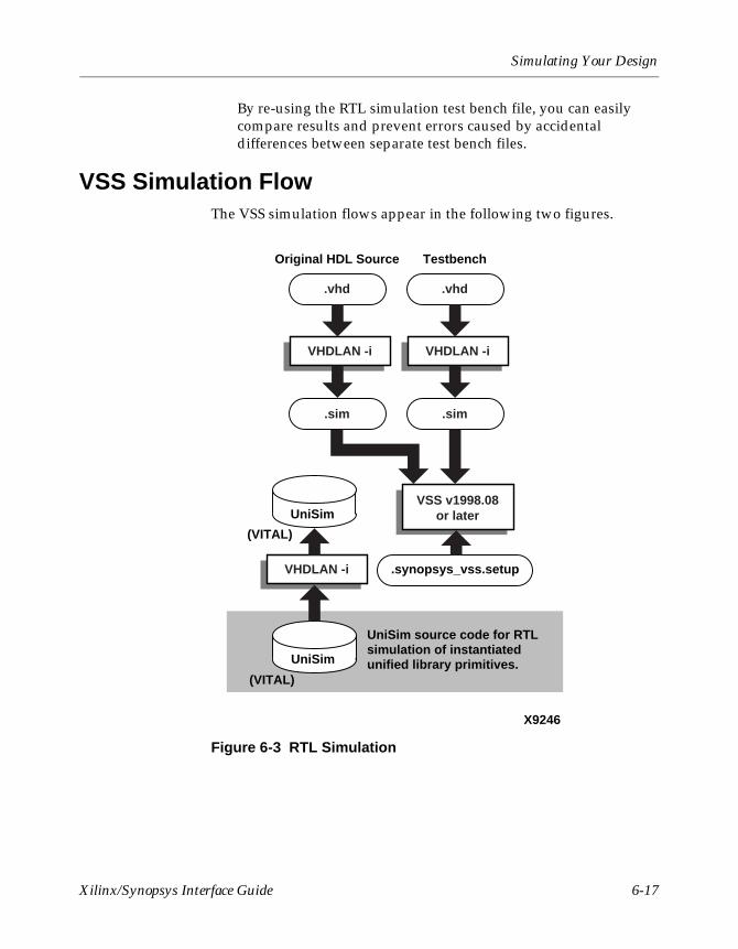
Simulating Your Design
By re-using the RTL simulation test bench file, you can easily compare results and prevent errors caused by accidental differences between separate test bench files.
VSS Simulation FlowThe VSS simulation flows appear in the following two figures.
Figure 6-3 RTL Simulation
X9246
UniSim
(VITAL)
(VITAL)
Original HDL Source Testbench
UniSim source code for RTL simulation of instantiated unified library primitives.
.synopsys_vss.setup
VSS v1998.08or later
.sim .sim
VHDLAN -i VHDLAN -i
.vhd .vhd
VHDLAN -i
UniSim
Xilinx/Synopsys Interface Guide 6-17
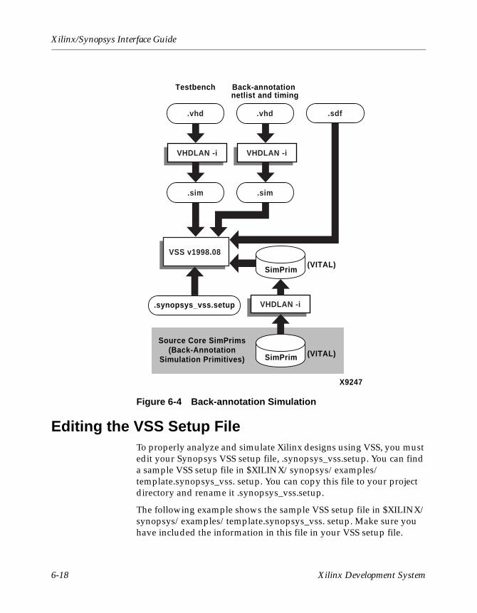
Xilinx/Synopsys Interface Guide
Figure 6-4 Back-annotation Simulation
Editing the VSS Setup FileTo properly analyze and simulate Xilinx designs using VSS, you must edit your Synopsys VSS setup file, .synopsys_vss.setup. You can find a sample VSS setup file in $XILINX/synopsys/examples/template.synopsys_vss. setup. You can copy this file to your project directory and rename it .synopsys_vss.setup.
The following example shows the sample VSS setup file in $XILINX/synopsys/examples/template.synopsys_vss. setup. Make sure you have included the information in this file in your VSS setup file.
X9247
Source Core SimPrims(Back-Annotation
Simulation Primitives)
VHDLAN -i
SimPrim
(VITAL)
(VITAL)
.synopsys_vss.setup
Testbench
.sim
VHDLAN -i
.vhd
SimPrim
.sim
VHDLAN -i
.vhd
Back-annotation netlist and timing
.sdf
VSS v1998.08
6-18 Xilinx Development System
Simulating Your Design
-- =================================================== ---- Template .synopsys_vss.setup file for Xilinx design ---- For use with Synopsys VSS. ---- =================================================== ---- =================================================== ---- Set any simulation preferences. ---- =================================================== --CS_COMPILED = FALSETIMEBASE = NSTIME_RES_FACTOR = 0.1-- ================================================== ---- Define a work library in the current project dir ---- to hold temporary files and keep the project area ---- uncluttered. Note: You must create a subdirectory ---- in your project directory called WORK. ---- ================================================== --WORK > DEFAULTDEFAULT : ./WORK-- ================================================== ---- Note that the following simulation libraries are ---- provided ready-analyzed with VSS v9701. If you’re ---- using a later version of VSS then refer to the ---- automatic compile scripts provided in the ---- appropriate library’s source directory, e.g. ---- $XILINX/synopsys/libraries/sim/src/unisims ---- ================================================== --UNISIM : $XILINX/synopsys/libraries/sim/lib/unisims
-- ================================================== ---- VITAL SimPrim libraries provided to support back- ---- annotated simulation only. ---- ================================================== --SIMPRIM : $XILINX/synopsys/libraries/sim/lib/simprims-- ================================================== ---- Packages used by LogiBLOX functional simulation ---- models only. I.e. To support behavioral simulation ---- of VHDL designs with instantiated LogiBLOX cells. ---- ================================================== --LOGIBLOX : $XILINX/synopsys/libraries/sim/lib/logiblox
-- ================================================== ---- Xilinx XC9000 FTGS simulation libraries. --
Xilinx/Synopsys Interface Guide 6-19
Xilinx/Synopsys Interface Guide
-- ================================================== --XC9000 : $XILINX/synopsys/libraries/sim/lib/xc9000/ftgs
Creating a Testbench FileFollow the instructions in the testbench.vhd file included with the stopwatch tutorial to create a testbench file for your design. See the XSI tutorial at http://support.xilinx.com/support/techsup/tutorials/index.htm for more information about creating a testbench for Xilinx devices. You can use the same testbench for RTL and timing simulation.
After you have created a testbench file, you can begin using the VSS simulator for RTL simulation.
Using RTL SimulationUse RTL simulation to debug your logic before fitting your design into an FPGA.
Generally RTL level simulation does not require VITAL or Verilog unified library models because VHDL simulators can simulate behavioral code. However if your design contains instantiated components (such as RAMs, ROMs, input registers, INFF, clock buffers), the simulator must have access to VITAL or Verilog models for these front end unified library components.
During simulation, analyze your design’s modules according to hierarchical precedence with the lowest first (analyze the testbench last). Analyze the RTL models for all instantiated primitives, followed by the design files, with the Synopsys VHDLAN command.
vhdlan –i module.vhd
.
.
.
vhdlan –i testbench.vhd
6-20 Xilinx Development System
Simulating Your Design
Note: Use the –i option on the VHDLAN command. While this option can result in a slight increase in simulation time, it is not dependent on any operating system or C compilers. Additionally, VHDLAN can analyze your design in compiled or interpretive modes. While the compiled mode usually accelerates simulation run times, it reduces debugger visibility into the simulation. For more information, refer to the Synopsys documentation.
After analyzing all your design modules (including the testbench), start the simulator. The simulator comes in two versions, a graphic debugging environment, VHDLDBX, and a command-line driven simulator, VHDLSIM. VHDLDBX allows you to select the desired configuration from a graphic window. VHDLSIM requires you to specify the desired configuration at the command line. In either case, select the configuration name associated with your testbench entity.
For example, consider a testbench with the following entity and architecture statements.
entity my_testbench isend my_testbench;architecture my_vectors of my_testbench is..begin..end my_vectors;
At a minimum, you then require a configuration of the following type.
Configuration my_configuration of my_testbench is for my_vectors end for;end my_configuration;
To start VHDLDBX on this design, perform the following steps.
1. Enter the following at the UNIX command line.
vhdldbx
2. Select my_configuration from the command list.
3. Press OK.
Xilinx/Synopsys Interface Guide 6-21
Xilinx/Synopsys Interface Guide
To start VHDLSIM on this design, enter the following command at the UNIX command line.
vhdlsim my_configuration
For an example of how to use these tools, refer to the XSI tutorial at http://support.xilinx.com/support/techsup/tutorials/index.htm. Also, see the Synopsys user documentation for more information.
The stopwatch tutorial provides the behv_sim.csh script file. This script illustrates the necessary steps to perform an RTL simulation on the stopwatch design. You can modify behv_sim.csh to use with your designs. This script analyzes the VHDL files, and starts the VSS VHDL Debugger (VHDLDBX). During simulation, the testbench applies stimulus to the design, and monitors and records its outputs.
Implementing Your DesignAfter debugging your design using RTL simulation, you can compile it using synthesis and implement it in an FPGA using the Xilinx software. You must implement your design before performing timing simulation.
Use DC Shell commands or Design Analyzer, as described in the “Synthesizing Your Design with FPGA Compiler and Design Compiler” chapter, to create the XNF or EDIF netlist file required by the Xilinx software. This gate-level netlist file contains components from the appropriate library but not timing information. The Xilinx software processes the netlist file and places the logical design into the physical architecture of your target FPGA.
After the Xilinx software implements the design, the actual target device timing information is available for timing simulation.
Using the stopwatch design as an example, the following steps provide an overview of the implementation procedure.
1. Compile the design, targeting the appropriate libraries, and create an XNF or EDIF netlist by executing the following command at the command line.
dc_shell –f watch.script
During processing, the system displays informational messages.
2. Run NGDBuild to process the netlist. NGDBuild translates the Synopsys-generated netlist to a Xilinx netlist.
6-22 Xilinx Development System
Simulating Your Design
ngdbuild –p parttype watch
3. Run the MAP program. MAP allocates the logic to CLBs and IOBs.
map watch
4. Run PAR, which produces a placed and routed design. The –w option specifies the output file name.
PAR watch –w watch_routed
5. Run NGDAnno, which relates the placed and routed design with the original design to ensure the retention of as many of the original component and net names as possible.
ngdanno watch_routed watch
6. Run NGD2VHDL, which creates a structural VHDL netlist for use as a simulation model and a corresponding SDF file containing timing information.
ngd2vhdl watch_routed
When simulating, you must analyze your design’s modules according to hierarchical precedence with the lowest first (structural netlist first, followed by the testbench).
vhdlan –i routed_design.vhd
vhdlan –i testbench.vhd
Note: VHDLAN can analyze your design in compiled or interpretive modes. While the compiled mode usually accelerates simulation run times, it reduces debugger visibility into the simulation. For more information, refer to the Synopsys documentation.
The VHDL Simulator launches and reads in the testbench, the back-annotated VHDL model for your placed and routed design, and the associated SDF file.
For timing simulation, the simulator starts in the same way as for RTL simulation, but with the addition of the following two command line options.
• The name of the SDF file that contains the timing information
• The instance in the testbench where you apply timing information
Xilinx/Synopsys Interface Guide 6-23
Xilinx/Synopsys Interface Guide
The following examples illustrate these two command line options.
• VHDLSIM Example
vhdlsim –sdf_top my_testbench/instance_name \
–sdf routed_design.sdf my_configuration
• VHDLDBX Example
vhdldbx –sdf_top my_testbench/instance_name \
–sdf routed_design.sdf my_configuration
Where instance_name is the instance name of the unit under test in your testbench.
Note: You can also specify the –sdf_top and –sdf options in the arguments field of the initial window that appears when you start VHDLDBX.
The stopwatch tutorial provides the tim_sim.csh script file. This script provides the necessary steps to perform a timing simulation with the VSS simulator. You can modify this script to use with your designs. You can use the same testbench you used to perform an RTL simulation to perform a timing simulation.
6-24 Xilinx Development System
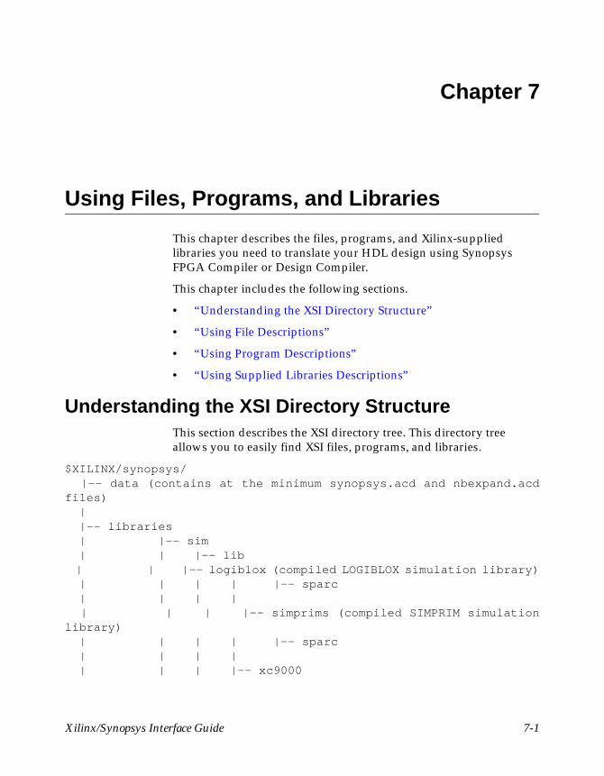
Chapter 7
Using Files, Programs, and Libraries
This chapter describes the files, programs, and Xilinx-supplied libraries you need to translate your HDL design using Synopsys FPGA Compiler or Design Compiler.
This chapter includes the following sections.
• “Understanding the XSI Directory Structure”
• “Using File Descriptions”
• “Using Program Descriptions”
• “Using Supplied Libraries Descriptions”
Understanding the XSI Directory StructureThis section describes the XSI directory tree. This directory tree allows you to easily find XSI files, programs, and libraries.
$XILINX/synopsys/ |-- data (contains at the minimum synopsys.acd and nbexpand.acdfiles) | |-- libraries | |-- sim | | |-- lib | | |-- logiblox (compiled LOGIBLOX simulation library) | | | | |-- sparc | | | | | | | |-- simprims (compiled SIMPRIM simulationlibrary) | | | | |-- sparc | | | | | | | |-- xc9000
Xilinx/Synopsys Interface Guide 7-1
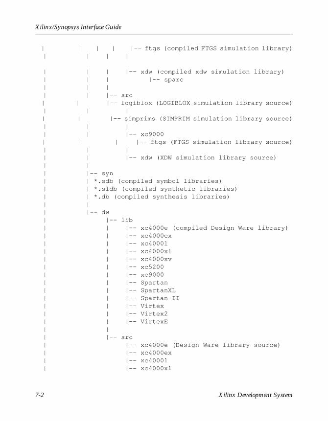
Xilinx/Synopsys Interface Guide
| | | | |-- ftgs (compiled FTGS simulation library) | | | | | | | |-- xdw (compiled xdw simulation library) | | | |-- sparc | | | | | |-- src | | |-- logiblox (LOGIBLOX simulation library source) | | | | | |-- simprims (SIMPRIM simulation library source) | | | | | |-- xc9000 | | | |-- ftgs (FTGS simulation library source) | | | | | |-- xdw (XDW simulation library source) | | | |-- syn | | *.sdb (compiled symbol libraries) | | *.sldb (compiled synthetic libraries) | | *.db (compiled synthesis libraries) | | | |-- dw | |-- lib | | |-- xc4000e (compiled Design Ware library) | | |-- xc4000ex | | |-- xc4000l | | |-- xc4000xl | | |-- xc4000xv | | |-- xc5200 | | |-- xc9000 | | |-- Spartan | | |-- SpartanXL | | |-- Spartan-II | | |-- Virtex | | |-- Virtex2 | | |-- VirtexE | | | |-- src | |-- xc4000e (Design Ware library source) | |-- xc4000ex | |-- xc4000l | |-- xc4000xl
7-2 Xilinx Development System
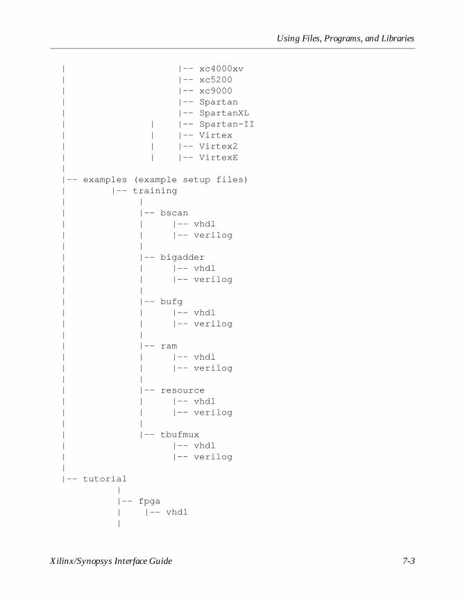
Using Files, Programs, and Libraries
| |-- xc4000xv | |-- xc5200 | |-- xc9000 | |-- Spartan | |-- SpartanXL | | |-- Spartan-II | | |-- Virtex | | |-- Virtex2 | | |-- VirtexE | |-- examples (example setup files) | |-- training | | | |-- bscan | | |-- vhdl | | |-- verilog | | | |-- bigadder | | |-- vhdl | | |-- verilog | | | |-- bufg | | |-- vhdl | | |-- verilog | | | |-- ram | | |-- vhdl | | |-- verilog | | | |-- resource | | |-- vhdl | | |-- verilog | | | |-- tbufmux | |-- vhdl | |-- verilog | |-- tutorial | |-- fpga | |-- vhdl |
Xilinx/Synopsys Interface Guide 7-3
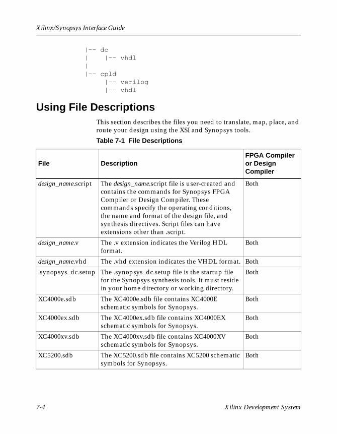
Xilinx/Synopsys Interface Guide
|-- dc | |-- vhdl | |-- cpld |-- verilog |-- vhdl
Using File DescriptionsThis section describes the files you need to translate, map, place, and route your design using the XSI and Synopsys tools.
Table 7-1 File Descriptions
File DescriptionFPGA Compiler or Design Compiler
design_name.script The design_name.script file is user-created and contains the commands for Synopsys FPGA Compiler or Design Compiler. These commands specify the operating conditions, the name and format of the design file, and synthesis directives. Script files can have extensions other than .script.
Both
design_name.v The .v extension indicates the Verilog HDL format.
Both
design_name.vhd The .vhd extension indicates the VHDL format. Both
.synopsys_dc.setup The .synopsys_dc.setup file is the startup file for the Synopsys synthesis tools. It must reside in your home directory or working directory.
Both
XC4000e.sdb The XC4000e.sdb file contains XC4000E schematic symbols for Synopsys.
Both
XC4000ex.sdb The XC4000ex.sdb file contains XC4000EX schematic symbols for Synopsys.
Both
XC4000xv.sdb The XC4000xv.sdb file contains XC4000XV schematic symbols for Synopsys.
Both
XC5200.sdb The XC5200.sdb file contains XC5200 schematic symbols for Synopsys.
Both
7-4 Xilinx Development System
Using Files, Programs, and Libraries
XC3000a.sdb The XC3000a.sdb file contains XC3000A schematic symbols for Synopsys.
Both
spartan.sdb The spartan.sdb file contains Spartan schematic symbols for Synopsys.
Both
spartanxl.sdb The spartanxl.sdb file contains SpartanXL schematic symbols for Synopsys.
Both
virtex.sdb The virtex.sdb file contains Virtex schematic symbols for Synopsys.
Both
XC9000.sdb The XC9000.sdb file contains XC9000 schematic symbols for Synopsys.
Both
.sim VSS simulation uses SIM files. Both
design_name.sxnf The design_name.sxnf file is the synthesized design generated by the Synopsys synthesis tools.
FPGA Compiler
design_name.sedif The design_name.sedif file is the synthesized design generated by the Synopsys synthesis tools using the EDIF syntax.
Design Compiler
design_name.ncf DC2NCF creates the design_name.ncf file. DC2NCF converts timing constraints applied to your design in the Synopsys environment to equivalent constraints that control the Xilinx place and route process.
Both
design_name.ngo EDIF2NGD or XNF2NGD create the design_name.ngo file, which contains a logical description of your design in terms of its original components and hierarchy.
Both
design_name.ngd The NGDBuild program generates the design_name.ngd file, a binary file containing a logical description of your design in terms of both its original components and hierarchy, and the NGD primitives to which your design is reduced.
Both
Table 7-1 File Descriptions
File DescriptionFPGA Compiler or Design Compiler
Xilinx/Synopsys Interface Guide 7-5
Xilinx/Synopsys Interface Guide
Using Program DescriptionsThis section describes the programs you use when translating, mapping, placing, and routing your design using the XSI and Synopsys tools. You can use the following programs with both Design Compiler and FPGA Compiler
design_name.ncd The MAP program generates the design_name.ncd file, a physical description of your design in terms of the components in the target Xilinx device.
Both
design_routed.ncd The design_routed.ncd file, generated by PAR, is your placed and routed design.
Both
design_name.nga NGDAnno generates the design_name.nga file, a back-annotated NGD file.
Both
design_name.vhd This file is the VHDL timing simulation model created by the NGD2VHDL program.
Both
design_name.sdf This file is the timing back-annotation file created by the NGD2VHDL program.
Both
Table 7-2 Program Descriptions
Program Description
Design Analyzer Design Analyzer is the Synopsys graphic interface to the Synopsys synthesis tools.
DC Shell DC Shell is the Synopsys UNIX command-line interface for entering commands, arguments, and options to the Synopsys synthesis tools.
Synlibs This program displays the target and link libraries for the specified part type and speed grade. You can append the output of the Synlibs command to the .synopsys_dc.setup file.You must list the libraries in your setup file in the order that they appear in the Synlibs output.
VHDLAN The VHDLAN program analyzes a VHD source file for simulation. Use the –i option with this program.
Table 7-1 File Descriptions
File DescriptionFPGA Compiler or Design Compiler
7-6 Xilinx Development System
Using Files, Programs, and Libraries
Using Supplied Libraries DescriptionsThis section describes the Xilinx-supplied libraries and supported part types and speed grades. Table 7-3 contains the following variables.
• family refers to the family of Xilinx devices, for example, 4000e, 4000ex, or 3000a.
• parttype refers to the specific Xilinx device, for example, 4003e, 4005e, or 3120a.
• 4kparttype refers to the specific Xilinx XC4000 device, for example, 4003e or 4005e.
VHDLDBX The VHDLDBX program is the VHDL Debugger, a graphic interface to the VHDL simulator. Through its dialog box, you can issue simulator commands, view command output, and view source code.
NGDBUILD This program reads a netlist file in XNF or EDIF format and creates an NGD file describing a logical design.
DC2NCF This program translates a Synopsys DC file to a netlist constraints file (NCF) file. The DC file is a Synopsys file containing your design constraints.
MAP This program maps a logical design to a Xilinx FPGA.
TRACE This program provides static timing analysis of your design based on input timing constraints.
PAR This program takes an NCD file, places and routes the design, and outputs an NCD file, which is then used by the BitGen program.
NGDAnno This program distributes delays, setup and hold times, and pulse widths found in the physical NCD design file back to the logical NGD file.
NGD2VHDL or NGD2VER
These programs convert Xilinx NGD format into structural HDL for gate-level simulation. Netlist consists of SimPrims.
BitGen This program produces a bitstream for Xilinx device configuration. It takes a fully routed NCD file as its input and creates a configuration bitstream.
Table 7-2 Program Descriptions
Program Description
Xilinx/Synopsys Interface Guide 7-7
Xilinx/Synopsys Interface Guide
• –s indicates the part type’s speed grade, for example, –5. Not all speed grades are available for all part types. Run Synlibs with the –h option to get a listing of all available part type and speed grade combinations.
Table 7-3 Library Descriptions
Library DescriptionFPGA Compiler or Design Compiler
xgen_3000a.db The xgen_3000a.db library describes the XC3000a cells that do not contain timing information, for example, CLBMAP, PULLUP, net flags, and VCC.
Both
xgen_3000l.db The xgen_3000l.db library describes the XC3000l cells that do not contain timing information, for example, CLBMAP, PULLUP, net flags, and VCC.
Both
xgen_3100l.db The xgen_3100l.db library describes the XC3100l cells that do not contain timing information, for example, CLBMAP, PULLUP, net flags, and VCC.
Both
xgen_4000e.db The xgen_4000e.db library describes the XC4000e cells that do not contain timing information, for example, FMAP, PULLUP, and VCC.
Both
xgen_4000l.db The xgen_4000l.db library describes the XC4000l cells that do not contain timing information, for example, FMAP, PULLUP, and VCC.
Both
xgen_4000ex.db The xgen_4000ex.db library describes the XC4000ex cells that do not contain timing information, for example, FMAP, PULLUP, and VCC.
Both
xgen_4000xl.db The xgen_4000xl.db library describes the XC4000xl cells that do not contain timing information, for example, FMAP, PULLUP, and VCC.
Both
7-8 Xilinx Development System
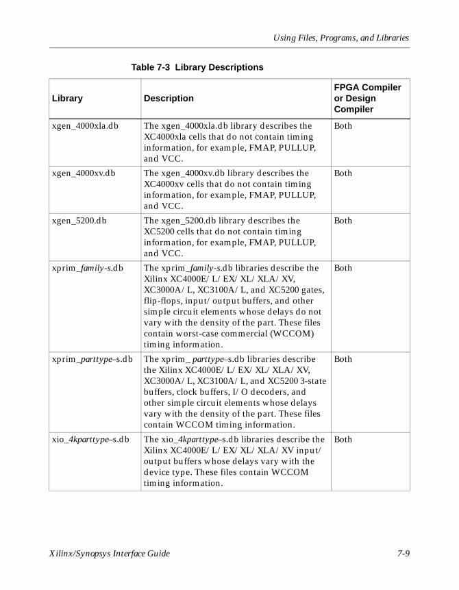
Using Files, Programs, and Libraries
xgen_4000xla.db The xgen_4000xla.db library describes the XC4000xla cells that do not contain timing information, for example, FMAP, PULLUP, and VCC.
Both
xgen_4000xv.db The xgen_4000xv.db library describes the XC4000xv cells that do not contain timing information, for example, FMAP, PULLUP, and VCC.
Both
xgen_5200.db The xgen_5200.db library describes the XC5200 cells that do not contain timing information, for example, FMAP, PULLUP, and VCC.
Both
xprim_family-s.db The xprim_family-s.db libraries describe the Xilinx XC4000E/L/EX/XL/XLA/XV, XC3000A/L, XC3100A/L, and XC5200 gates, flip-flops, input/output buffers, and other simple circuit elements whose delays do not vary with the density of the part. These files contain worst-case commercial (WCCOM) timing information.
Both
xprim_parttype–s.db The xprim_ parttype–s.db libraries describe the Xilinx XC4000E/L/EX/XL/XLA/XV, XC3000A/L, XC3100A/L, and XC5200 3-state buffers, clock buffers, I/O decoders, and other simple circuit elements whose delays vary with the density of the part. These files contain WCCOM timing information.
Both
xio_4kparttype–s.db The xio_4kparttype–s.db libraries describe the Xilinx XC4000E/L/EX/XL/XLA/XV input/output buffers whose delays vary with the device type. These files contain WCCOM timing information.
Both
Table 7-3 Library Descriptions
Library DescriptionFPGA Compiler or Design Compiler
Xilinx/Synopsys Interface Guide 7-9
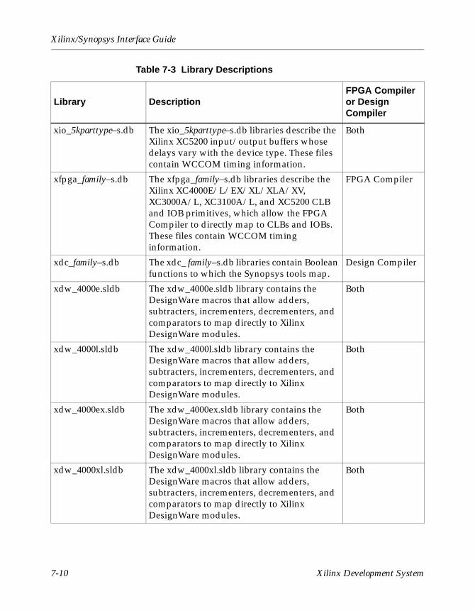
Xilinx/Synopsys Interface Guide
xio_5kparttype–s.db The xio_5kparttype–s.db libraries describe the Xilinx XC5200 input/output buffers whose delays vary with the device type. These files contain WCCOM timing information.
Both
xfpga_family–s.db The xfpga_family–s.db libraries describe the Xilinx XC4000E/L/EX/XL/XLA/XV, XC3000A/L, XC3100A/L, and XC5200 CLB and IOB primitives, which allow the FPGA Compiler to directly map to CLBs and IOBs. These files contain WCCOM timing information.
FPGA Compiler
xdc_family–s.db The xdc_ family–s.db libraries contain Boolean functions to which the Synopsys tools map.
Design Compiler
xdw_4000e.sldb The xdw_4000e.sldb library contains the DesignWare macros that allow adders, subtracters, incrementers, decrementers, and comparators to map directly to Xilinx DesignWare modules.
Both
xdw_4000l.sldb The xdw_4000l.sldb library contains the DesignWare macros that allow adders, subtracters, incrementers, decrementers, and comparators to map directly to Xilinx DesignWare modules.
Both
xdw_4000ex.sldb The xdw_4000ex.sldb library contains the DesignWare macros that allow adders, subtracters, incrementers, decrementers, and comparators to map directly to Xilinx DesignWare modules.
Both
xdw_4000xl.sldb The xdw_4000xl.sldb library contains the DesignWare macros that allow adders, subtracters, incrementers, decrementers, and comparators to map directly to Xilinx DesignWare modules.
Both
Table 7-3 Library Descriptions
Library DescriptionFPGA Compiler or Design Compiler
7-10 Xilinx Development System
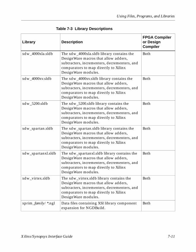
Using Files, Programs, and Libraries
xdw_4000xla.sldb The xdw_4000xla.sldb library contains the DesignWare macros that allow adders, subtracters, incrementers, decrementers, and comparators to map directly to Xilinx DesignWare modules.
Both
xdw_4000xv.sldb The xdw_4000xv.sldb library contains the DesignWare macros that allow adders, subtracters, incrementers, decrementers, and comparators to map directly to Xilinx DesignWare modules.
Both
xdw_5200.sldb The xdw_5200.sldb library contains the DesignWare macros that allow adders, subtracters, incrementers, decrementers, and comparators to map directly to Xilinx DesignWare modules.
Both
xdw_spartan.sldb The xdw_spartan.sldb library contains the DesignWare macros that allow adders, subtracters, incrementers, decrementers, and comparators to map directly to Xilinx DesignWare modules.
Both
xdw_spartanxl.sldb The xdw_spartanxl.sldb library contains the DesignWare macros that allow adders, subtracters, incrementers, decrementers, and comparators to map directly to Xilinx DesignWare modules.
Both
xdw_virtex.sldb The xdw_virtex.sldb library contains the DesignWare macros that allow adders, subtracters, incrementers, decrementers, and comparators to map directly to Xilinx DesignWare modules.
Both
xprim_family/*.ngl Data files containing XSI library component expansion for NGDBuild.
Both
Table 7-3 Library Descriptions
Library DescriptionFPGA Compiler or Design Compiler
Xilinx/Synopsys Interface Guide 7-11
Xilinx/Synopsys Interface Guide
Finding Supported Part Types and Speed GradesRun Synlibs with the –h option to get a listing of all available part type and speed grade combinations. You can also refer to the Xilinx online Data Book at http://www.xilinx.com for current speed grade information.
Finding Unsupported Part Types and Speed GradesIf designing for a part type or speed grade for which no libraries are available, use the libraries for the closest part type or speed grade in the same family. Indicate the part type or speed grade actually used when you run PAR. The timing constraints in the NCF file can need adjustment.
Note: For more information on specifying the part type, refer to the Development System Reference Guide.
7-12 Xilinx Development System
Appendix A
XSI Library Primitives
You can find the XSI primitives in the XSI-supplied libraries in FPGA Compiler and FPGA Express; you can instantiate them in your VHDL or Verilog HDL file. Use the synlibs program to list the appropriate libraries for a specific part type. Refer to the “Getting Started” chapter for information on how to use synlibs.
In the primitive tables in this appendix, the names of the inputs and outputs follow the primitive names, the applicable architecture, and any important notes. All primitives in the libraries contain timing parameters. The Notes column includes specific timing details and additional functional information.
Although Synopsys cannot synthesize some primitives (primitives with the Dont Touch and Dont Use attributes), you can instantiate them. An asterisk (*) next to the primitive name indicates that you can instantiate it. Refer to the Synopsys documentation for more information on the Dont Touch and Dont Use attributes. Use the name of a primitive to instantiate it. In addition, you must identify the signals connected to the input and output pins when instantiating a primitive.
In general, pins are organized with data pins before control pins. When several pins are part of a bus, they are listed with the MSB first. Buses of four or more bits follow bus notation, for example, A<7:0>. Buses with fewer bits are kept as separate signals.
Synopsys FPGA Compiler II does not recognize the underscore character (“_”) as valid.
Xilinx/Synopsys Interface Guide A-1
Xilinx/Synopsys Interface Guide
The following sections are included in this appendix.
• “Generating a List of XSI Library Primitives”
• “Obtaining XSI Library Primitive Pin Order”
• “Understanding Virtex-Specific Cell Names”
• “Xilinx DesignWare Modules”
• “Post-Configuration Initialization States”
Generating a List of XSI Library PrimitivesYou can use the following procedure to generate a list of the XSI library primitives provided in this appendix.
1. Start DC Shell or Design Analyzer in a directory that contains your .synopsys_dc.setup file. Ensure this setup file points to the libraries you need to synthesize your designs in the XSI design flow.
2. In the command window of Design Analyzer or in DC Shell, enter the following command.
read –f db link_library
3. In the command window of Design Analyzer or in DC Shell, enter the following command.
list –files
This command lists all the library files in memory.
4. For each item in the list, enter the following command.
find cell filename/*
filename is the .db library file.
For example, for the library file xfpga_4000e-3.db the Find Cell command lists the following.
xfpga_4000e-3/clb_4000
xfpga_4000e-3/iob_4000
The library file lists first, followed by the library primitive.
A-2 Xilinx Development System

XSI Library Primitives
Obtaining XSI Library Primitive Pin OrderPositional notation allows you to instantiate a primitive without explicitly specifying the pins for that component. To use this notation, you must know the pin order of the primitive. You can use the following procedure to obtain the pin order for any of the XSI library primitives provided in this appendix.
1. Start DC Shell or Design Analyzer in a directory that contains your .synopsys_dc.setup file.
2. In DC Shell or in the command window of Design Analyzer, enter the following command.
read –f db link_library
3. In DC Shell or in the command window of Design Analyzer, enter the following command.
list –files
This command lists all the library files in memory. Know which file contains the relevant primitive.
4. In DC Shell or in the command window of Design Analyzer, enter the following command.
find (pin, “dbfilename/cellname/*”)
dbfilename is the name of the .db file that contains the primitive and cellname is the relevant primitive.
For example, the following command finds the pin order of the OR2 primitive in the XC4000EX library.
find (pin, “xprim_4000ex-3/OR2/*”)
This results in the following pin order.
{“O” “I1” “I0”}
Alphabetical List of Primitives for All ArchitecturesThis section lists the XSI primitives in alphabetical order with their associated output, input, and bidirectional pins. In addition, the pins are listed in the order used for positional notation. For example, the pins for ACLK are listed with the O pin first, followed by the I pin. Therefore, you can instantiate ACLK with only the signal (wire)
Xilinx/Synopsys Interface Guide A-3
Xilinx/Synopsys Interface Guide
names; you do not need to declare the ACLK pins. You can also find the applicable architecture and any notes in the tables included in this section.
Using the Dont Touch AttributeAn asterisk (*) next to a primitive name indicates that you must instantiate it. Also, you must apply the Dont Touch attribute to instantiated primitives. Refer to the Synopsys documentation for more information on the Dont Touch attribute.
Synopsys FPGA Compiler II does not recognize the underscore character (“_”) as valid.
Setting the INIT AttributeBefore you can apply the INIT attribute to instantiated RAM and ROM primitives, you must modify the Synopsys dc.setup_dc file, which resides in $XILINX/synopsys/examples/template.synopsys_dc_setup_fc. Change the following line in that file.
edifout_write_properties_list = “instance_number \pad_location part”
The new line, after the changes, appears as follows.
edifout_write_properties_list = “instance_number \pad_location part” “INIT”
Primitive Name SuffixesThe following table lists the primitive name suffixes and their corresponding descriptions.
Table A-1 Primitive Name Suffixes
Suffix Description
I Inverted global reset (INIT=S)
_F Fast implementation of clock buffer (using dedicated input clock pad) or fast slew rate for output buffers; NODELAY attribute added for input registers
A-4 Xilinx Development System
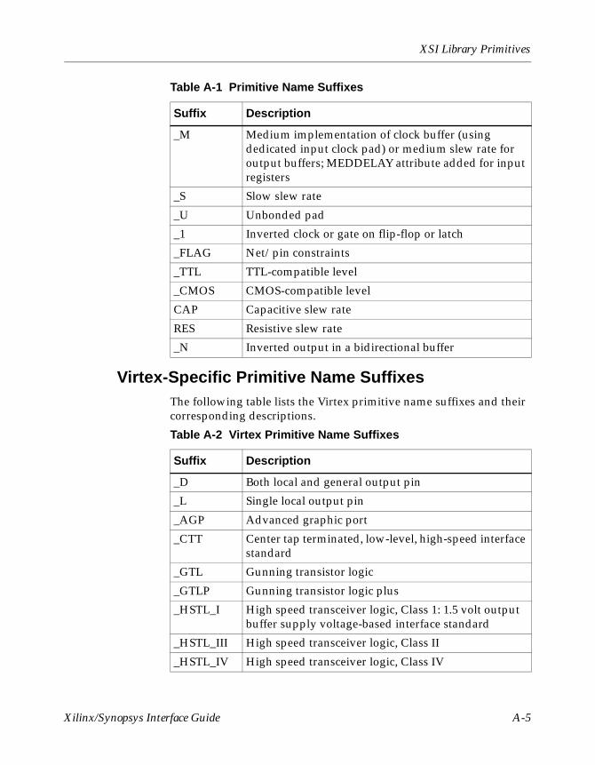
XSI Library Primitives
Virtex-Specific Primitive Name SuffixesThe following table lists the Virtex primitive name suffixes and their corresponding descriptions.
_M Medium implementation of clock buffer (using dedicated input clock pad) or medium slew rate for output buffers; MEDDELAY attribute added for input registers
_S Slow slew rate
_U Unbonded pad
_1 Inverted clock or gate on flip-flop or latch
_FLAG Net/pin constraints
_TTL TTL-compatible level
_CMOS CMOS-compatible level
CAP Capacitive slew rate
RES Resistive slew rate
_N Inverted output in a bidirectional buffer
Table A-2 Virtex Primitive Name Suffixes
Suffix Description
_D Both local and general output pin
_L Single local output pin
_AGP Advanced graphic port
_CTT Center tap terminated, low-level, high-speed interface standard
_GTL Gunning transistor logic
_GTLP Gunning transistor logic plus
_HSTL_I High speed transceiver logic, Class 1: 1.5 volt output buffer supply voltage-based interface standard
_HSTL_III High speed transceiver logic, Class II
_HSTL_IV High speed transceiver logic, Class IV
Table A-1 Primitive Name Suffixes
Suffix Description
Xilinx/Synopsys Interface Guide A-5
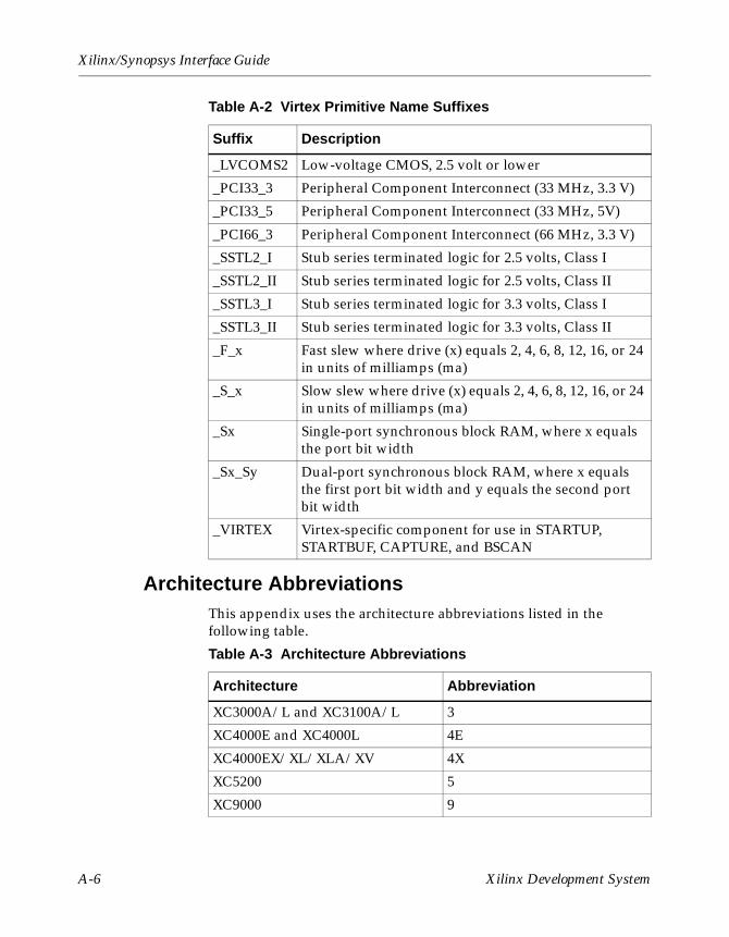
Xilinx/Synopsys Interface Guide
Architecture AbbreviationsThis appendix uses the architecture abbreviations listed in the following table.
_LVCOMS2 Low-voltage CMOS, 2.5 volt or lower
_PCI33_3 Peripheral Component Interconnect (33 MHz, 3.3 V)
_PCI33_5 Peripheral Component Interconnect (33 MHz, 5V)
_PCI66_3 Peripheral Component Interconnect (66 MHz, 3.3 V)
_SSTL2_I Stub series terminated logic for 2.5 volts, Class I
_SSTL2_II Stub series terminated logic for 2.5 volts, Class II
_SSTL3_I Stub series terminated logic for 3.3 volts, Class I
_SSTL3_II Stub series terminated logic for 3.3 volts, Class II
_F_x Fast slew where drive (x) equals 2, 4, 6, 8, 12, 16, or 24 in units of milliamps (ma)
_S_x Slow slew where drive (x) equals 2, 4, 6, 8, 12, 16, or 24 in units of milliamps (ma)
_Sx Single-port synchronous block RAM, where x equals the port bit width
_Sx_Sy Dual-port synchronous block RAM, where x equals the first port bit width and y equals the second port bit width
_VIRTEX Virtex-specific component for use in STARTUP, STARTBUF, CAPTURE, and BSCAN
Table A-3 Architecture Abbreviations
Architecture Abbreviation
XC3000A/L and XC3100A/L 3
XC4000E and XC4000L 4E
XC4000EX/XL/XLA/XV 4X
XC5200 5
XC9000 9
Table A-2 Virtex Primitive Name Suffixes
Suffix Description
A-6 Xilinx Development System
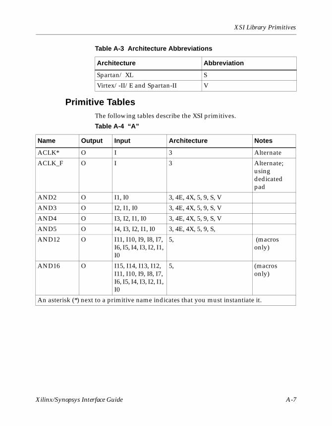
XSI Library Primitives
Primitive TablesThe following tables describe the XSI primitives.
Spartan/ XL S
Virtex/-II/E and Spartan-II V
Table A-4 “A”
Name Output Input Architecture Notes
ACLK* O I 3 Alternate
ACLK_F O I 3 Alternate; using dedicated pad
AND2 O I1, I0 3, 4E, 4X, 5, 9, S, V
AND3 O I2, I1, I0 3, 4E, 4X, 5, 9, S, V
AND4 O I3, I2, I1, I0 3, 4E, 4X, 5, 9, S, V
AND5 O I4, I3, I2, I1, I0 3, 4E, 4X, 5, 9, S,
AND12 O I11, I10, I9, I8, I7, I6, I5, I4, I3, I2, I1, I0
5, (macros only)
AND16 O I15, I14, I13, I12, I11, I10, I9, I8, I7, I6, I5, I4, I3, I2, I1, I0
5, (macros only)
An asterisk (*) next to a primitive name indicates that you must instantiate it.
Table A-3 Architecture Abbreviations
Architecture Abbreviation
Xilinx/Synopsys Interface Guide A-7
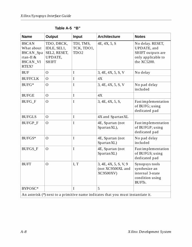
Xilinx/Synopsys Interface Guide
Table A-5 “B”
Name Output Input Architecture Notes
BSCANWhat about BSCAN_Spartan-II & BSCAN_VIRTEX?
TDO, DRCK, IDLE, SEL1, SEL2, RESET, UPDATE, SHIFT
TDI, TMS, TCK, TDO1, TDO2
4E, 4X, 5, S No delay. RESET, UPDATE, and SHIFT outputs are only applicable to the XC5200.
BUF O I 3, 4E, 4X, 5, S, V No delay
BUFFCLK O I 4X
BUFG* O I 3, 4E, 4X, 5, S, V No pad delay included
BUFGE O I 4X
BUFG_F O I 3, 4E, 4X, 5, S, Fast implementation of BUFG; using dedicated pad
BUFGLS O I 4X and SpartanXL
BUFGP_F O I 4E, Spartan (not SpartanXL),
Fast implementation of BUFGP; using dedicated pad
BUFGS* O I 4E, Spartan (not SpartanXL)
No pad delay included
BUFGS_F O I 4E, Spartan (not SpartanXL)
Fast implementation of BUFGS; using dedicated pad
BUFT O I, T 3, 4E, 4X, 5, S, V, 9 (not XC9500XL and XC9500XV)
Synopsys tools synthesize an internal 3-state condition using BUFTs.
BYPOSC* I 5
An asterisk (*) next to a primitive name indicates that you must instantiate it.
A-8 Xilinx Development System
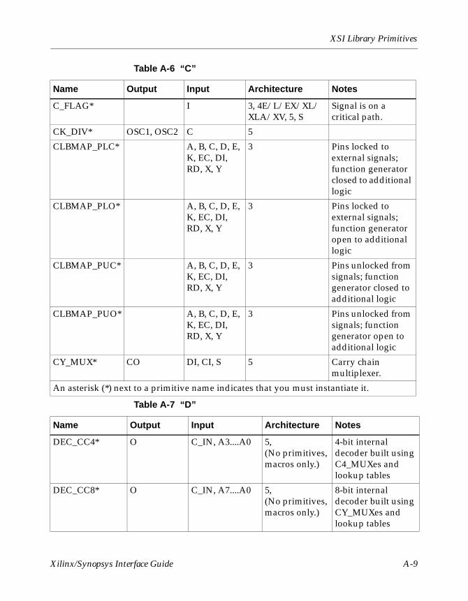
XSI Library Primitives
Table A-6 “C”
Name Output Input Architecture Notes
C_FLAG* I 3, 4E/L/EX/XL/XLA/XV, 5, S
Signal is on a critical path.
CK_DIV* OSC1, OSC2 C 5
CLBMAP_PLC* A, B, C, D, E, K, EC, DI, RD, X, Y
3 Pins locked to external signals; function generator closed to additional logic
CLBMAP_PLO* A, B, C, D, E, K, EC, DI, RD, X, Y
3 Pins locked to external signals; function generator open to additional logic
CLBMAP_PUC* A, B, C, D, E, K, EC, DI, RD, X, Y
3 Pins unlocked from signals; function generator closed to additional logic
CLBMAP_PUO* A, B, C, D, E, K, EC, DI, RD, X, Y
3 Pins unlocked from signals; function generator open to additional logic
CY_MUX* CO DI, CI, S 5 Carry chain multiplexer.
An asterisk (*) next to a primitive name indicates that you must instantiate it.
Table A-7 “D”
Name Output Input Architecture Notes
DEC_CC4* O C_IN, A3....A0 5, (No primitives, macros only.)
4-bit internal decoder built using C4_MUXes and lookup tables
DEC_CC8* O C_IN, A7....A0 5, (No primitives, macros only.)
8-bit internal decoder built using CY_MUXes and lookup tables
Xilinx/Synopsys Interface Guide A-9
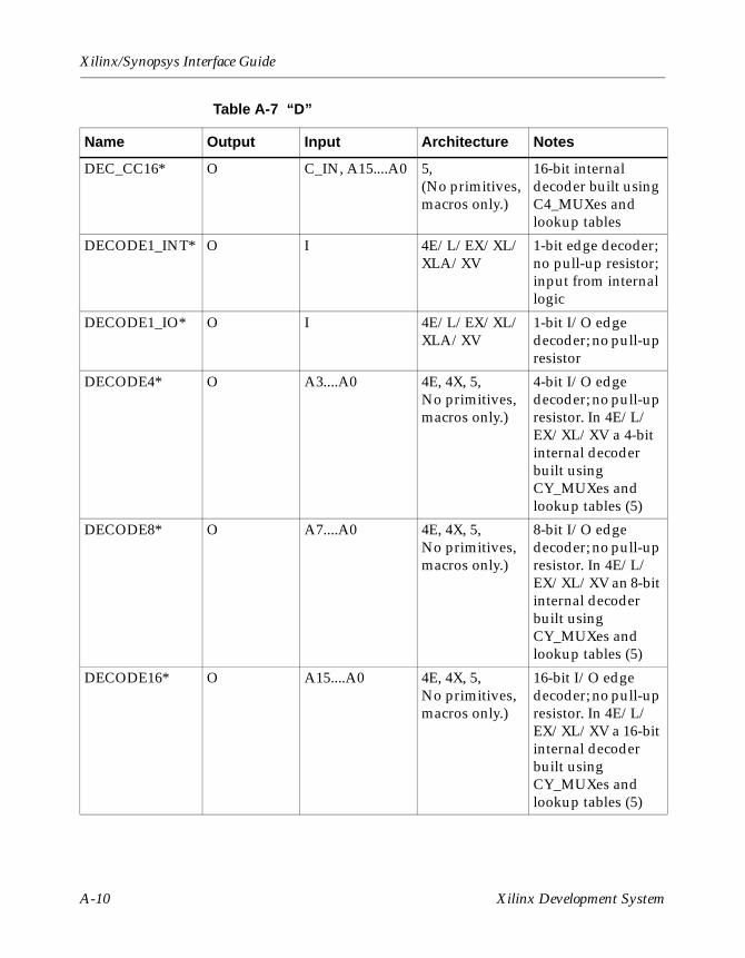
Xilinx/Synopsys Interface Guide
DEC_CC16* O C_IN, A15....A0 5, (No primitives, macros only.)
16-bit internal decoder built using C4_MUXes and lookup tables
DECODE1_INT* O I 4E/L/EX/XL/XLA/XV
1-bit edge decoder; no pull-up resistor; input from internal logic
DECODE1_IO* O I 4E/L/EX/XL/XLA/XV
1-bit I/O edge decoder; no pull-up resistor
DECODE4* O A3....A0 4E, 4X, 5, No primitives, macros only.)
4-bit I/O edge decoder; no pull-up resistor. In 4E/L/EX/XL/XV a 4-bit internal decoder built using CY_MUXes and lookup tables (5)
DECODE8* O A7....A0 4E, 4X, 5, No primitives, macros only.)
8-bit I/O edge decoder; no pull-up resistor. In 4E/L/EX/XL/XV an 8-bit internal decoder built using CY_MUXes and lookup tables (5)
DECODE16* O A15....A0 4E, 4X, 5, No primitives, macros only.)
16-bit I/O edge decoder; no pull-up resistor. In 4E/L/EX/XL/XV a 16-bit internal decoder built using CY_MUXes and lookup tables (5)
Table A-7 “D”
Name Output Input Architecture Notes
A-10 Xilinx Development System
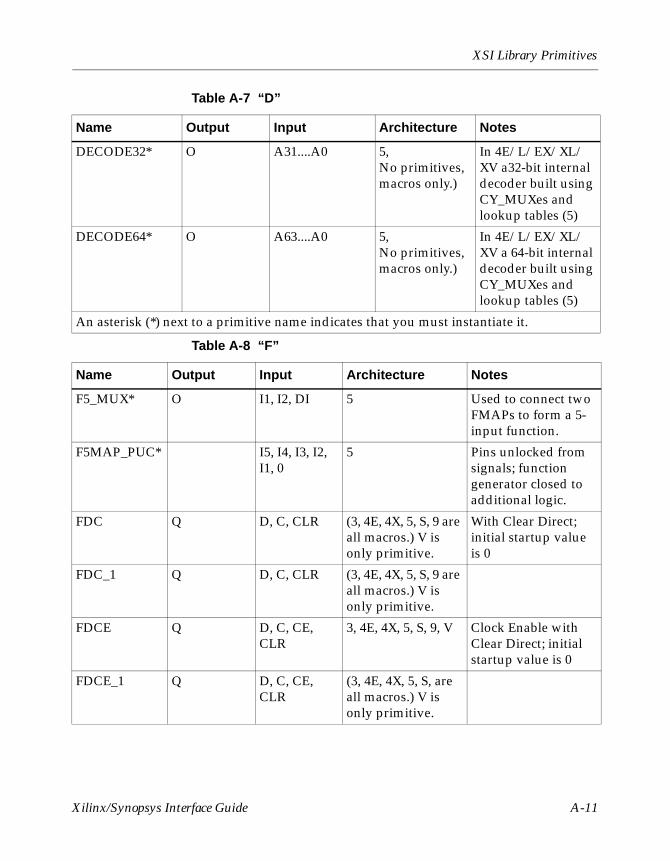
XSI Library Primitives
DECODE32* O A31....A0 5, No primitives, macros only.)
In 4E/L/EX/XL/XV a32-bit internal decoder built using CY_MUXes and lookup tables (5)
DECODE64* O A63....A0 5, No primitives, macros only.)
In 4E/L/EX/XL/XV a 64-bit internal decoder built using CY_MUXes and lookup tables (5)
An asterisk (*) next to a primitive name indicates that you must instantiate it.
Table A-8 “F”
Name Output Input Architecture Notes
F5_MUX* O I1, I2, DI 5 Used to connect two FMAPs to form a 5-input function.
F5MAP_PUC* I5, I4, I3, I2, I1, 0
5 Pins unlocked from signals; function generator closed to additional logic.
FDC Q D, C, CLR (3, 4E, 4X, 5, S, 9 are all macros.) V is only primitive.
With Clear Direct; initial startup value is 0
FDC_1 Q D, C, CLR (3, 4E, 4X, 5, S, 9 are all macros.) V is only primitive.
FDCE Q D, C, CE, CLR
3, 4E, 4X, 5, S, 9, V Clock Enable with Clear Direct; initial startup value is 0
FDCE_1 Q D, C, CE, CLR
(3, 4E, 4X, 5, S, are all macros.) V is only primitive.
Table A-7 “D”
Name Output Input Architecture Notes
Xilinx/Synopsys Interface Guide A-11
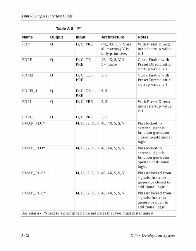
Xilinx/Synopsys Interface Guide
FDP Q D, C, PRE (4E, 4X, 5, S, 9 are all macros.) V is only primitive.
With Preset Direct; initial startup value is 1
FDPE Q D, C, CE, PRE
4E, 4X, S, V, 95 - macro
Clock Enable with Preset Direct; initial startup value is 1
FDPEI Q D, C, CE, PRE
3, 5 Clock Enable with Preset Direct; initial startup value is 1
FDPEI_1 Q D, C, CE, PRE
3, 5
FDPI Q D, C, PRE 3, 5 With Preset Direct; initial startup value is 1
FDPI_1 Q D, C, PRE 3, 5
FMAP_PLC* I4, I3, I2, I1, 0 4E, 4X, 5, S, V Pins locked to external signals; function generator closed to additional logic.
FMAP_PLO* I4, I3, I2, I1, 0 4E, 4X, 5, S, V Pins locked to external signals; function generator open to additional logic.
FMAP_PUC* I4, I3, I2, I1, 0 4E, 4X, 5, S, V Pins unlocked from signals; function generator closed to additional logic.
FMAP_PUO* I4, I3, I2, I1, 0 4E, 4X, 5, S, V Pins unlocked from signals; function generator open to additional logic.
An asterisk (*) next to a primitive name indicates that you must instantiate it.
Table A-8 “F”
Name Output Input Architecture Notes
A-12 Xilinx Development System
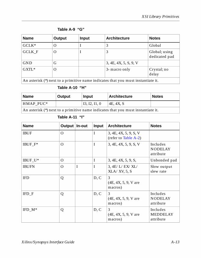
XSI Library Primitives
Table A-9 “G”
Name Output Input Architecture Notes
GCLK* O I 3 Global
GCLK_F O I 3 Global; using dedicated pad
GND G 3, 4E, 4X, 5, S, 9, V
GXTL* O 3- macro only Crystal; no delay
An asterisk (*) next to a primitive name indicates that you must instantiate it.
Table A-10 “H”
Name Output Input Architecture Notes
HMAP_PUC* I3, I2, I1, 0 4E, 4X, S
An asterisk (*) next to a primitive name indicates that you must instantiate it.
Table A-11 “I”
Name Output In-out Input Architecture Notes
IBUF O I 3, 4E, 4X, 5, 9, S, V (refer to Table A-2)
IBUF_F* O I 3, 4E, 4X, 5, 9, S, V Includes NODELAY attribute
IBUF_U* O I 3, 4E, 4X, 5, 9, S, Unbonded pad
IBUFN O I I 3, 4E/L/EX/XL/XLA/XV, 5, S
Slow output slew rate
IFD Q D, C 3(4E, 4X, 5, 9, V are macros)
IFD_F Q D, C 3(4E, 4X, 5, 9, V are macros)
Includes NODELAY attribute
IFD_M* Q D, C 3(4E, 4X, 5, 9, V are macros)
Includes MEDDELAY attribute
Xilinx/Synopsys Interface Guide A-13
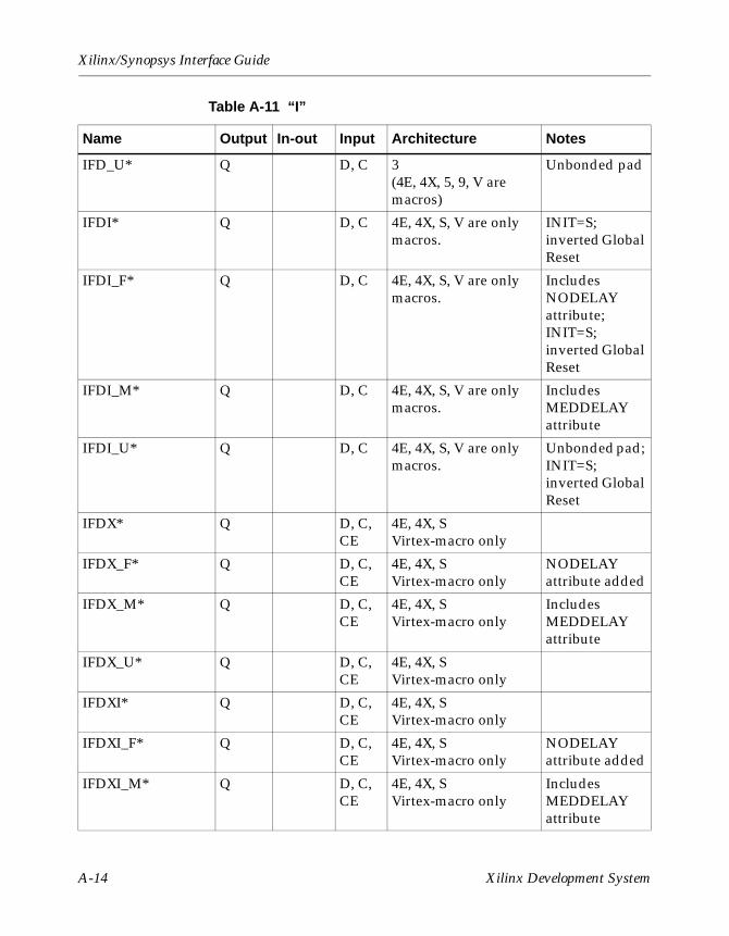
Xilinx/Synopsys Interface Guide
IFD_U* Q D, C 3(4E, 4X, 5, 9, V are macros)
Unbonded pad
IFDI* Q D, C 4E, 4X, S, V are only macros.
INIT=S; inverted Global Reset
IFDI_F* Q D, C 4E, 4X, S, V are only macros.
Includes NODELAY attribute; INIT=S; inverted Global Reset
IFDI_M* Q D, C 4E, 4X, S, V are only macros.
Includes MEDDELAY attribute
IFDI_U* Q D, C 4E, 4X, S, V are only macros.
Unbonded pad; INIT=S; inverted Global Reset
IFDX* Q D, C, CE
4E, 4X, SVirtex-macro only
IFDX_F* Q D, C, CE
4E, 4X, SVirtex-macro only
NODELAY attribute added
IFDX_M* Q D, C, CE
4E, 4X, SVirtex-macro only
Includes MEDDELAY attribute
IFDX_U* Q D, C, CE
4E, 4X, SVirtex-macro only
IFDXI* Q D, C, CE
4E, 4X, SVirtex-macro only
IFDXI_F* Q D, C, CE
4E, 4X, SVirtex-macro only
NODELAY attribute added
IFDXI_M* Q D, C, CE
4E, 4X, SVirtex-macro only
Includes MEDDELAY attribute
Table A-11 “I”
Name Output In-out Input Architecture Notes
A-14 Xilinx Development System
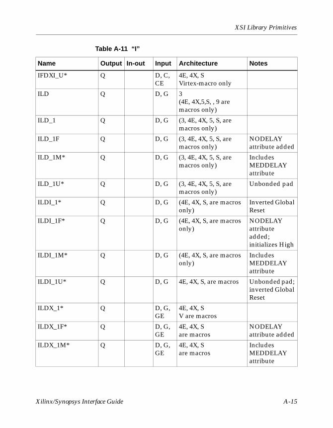
XSI Library Primitives
IFDXI_U* Q D, C, CE
4E, 4X, SVirtex-macro only
ILD Q D, G 3(4E, 4X,5,S, , 9 are macros only)
ILD_1 Q D, G (3, 4E, 4X, 5, S, are macros only)
ILD_1F Q D, G (3, 4E, 4X, 5, S, are macros only)
NODELAY attribute added
ILD_1M* Q D, G (3, 4E, 4X, 5, S, are macros only)
Includes MEDDELAY attribute
ILD_1U* Q D, G (3, 4E, 4X, 5, S, are macros only)
Unbonded pad
ILDI_1* Q D, G (4E, 4X, S, are macros only)
Inverted Global Reset
ILDI_1F* Q D, G (4E, 4X, S, are macros only)
NODELAY attribute added; initializes High
ILDI_1M* Q D, G (4E, 4X, S, are macros only)
Includes MEDDELAY attribute
ILDI_1U* Q D, G 4E, 4X, S, are macros Unbonded pad; inverted Global Reset
ILDX_1* Q D, G, GE
4E, 4X, SV are macros
ILDX_1F* Q D, G, GE
4E, 4X, Sare macros
NODELAY attribute added
ILDX_1M* Q D, G, GE
4E, 4X, Sare macros
Includes MEDDELAY attribute
Table A-11 “I”
Name Output In-out Input Architecture Notes
Xilinx/Synopsys Interface Guide A-15
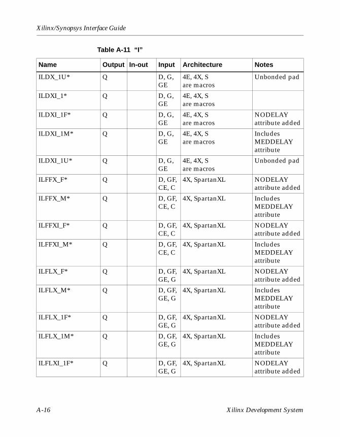
Xilinx/Synopsys Interface Guide
ILDX_1U* Q D, G, GE
4E, 4X, Sare macros
Unbonded pad
ILDXI_1* Q D, G, GE
4E, 4X, Sare macros
ILDXI_1F* Q D, G, GE
4E, 4X, Sare macros
NODELAY attribute added
ILDXI_1M* Q D, G, GE
4E, 4X, Sare macros
Includes MEDDELAY attribute
ILDXI_1U* Q D, G, GE
4E, 4X, Sare macros
Unbonded pad
ILFFX_F* Q D, GF, CE, C
4X, SpartanXL NODELAY attribute added
ILFFX_M* Q D, GF, CE, C
4X, SpartanXL Includes MEDDELAY attribute
ILFFXI_F* Q D, GF, CE, C
4X, SpartanXL NODELAY attribute added
ILFFXI_M* Q D, GF, CE, C
4X, SpartanXL Includes MEDDELAY attribute
ILFLX_F* Q D, GF, GE, G
4X, SpartanXL NODELAY attribute added
ILFLX_M* Q D, GF, GE, G
4X, SpartanXL Includes MEDDELAY attribute
ILFLX_1F* Q D, GF, GE, G
4X, SpartanXL NODELAY attribute added
ILFLX_1M* Q D, GF, GE, G
4X, SpartanXL Includes MEDDELAY attribute
ILFLXI_1F* Q D, GF, GE, G
4X, SpartanXL NODELAY attribute added
Table A-11 “I”
Name Output In-out Input Architecture Notes
A-16 Xilinx Development System
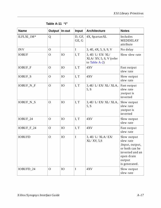
XSI Library Primitives
ILFLXI_1M* Q D, GF, GE, G
4X, SpartanXL Includes MEDDELAY attribute
INV O I 3, 4E, 4X, 5, S, 9, V No delay
IOBUF O IO I, T 3, 4E/L/EX/XL/XLA/XV, 5, S, V (refer to Table A-2)
Slow slew rate
IOBUF_F O IO I, T 4XV Fast output slew rate
IOBUF_S O IO I, T 4XV Slow output slew rate
IOBUF_N_F O IO I, T 3, 4E/L/EX/XL/XLA, 5, S
Fast output slew rate;output is inverted
IOBUF_N_S O IO I, T 3, 4E/L/EX/XL/XLA, 5, S
Slow output slew rate;output is inverted
IOBUF_24 O IO I, T 4XV Slow output slew rate
IOBUF_F_24 O IO I, T 4XV Fast output slew rate
IOBUFD O IO I 3, 4E/L/XLA/EX/XL/XV, 5,S
Slow output slew rate;Input, output, or both can be inverted and an open drain outputis generated.
IOBUFD_24 O IO I 4XV Slow output slew rate
Table A-11 “I”
Name Output In-out Input Architecture Notes
Xilinx/Synopsys Interface Guide A-17
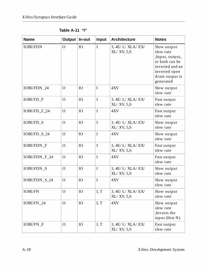
Xilinx/Synopsys Interface Guide
IOBUFDN O IO I 3, 4E/L/XLA/EX/XL/XV, 5,S
Slow output slew rate;Input, output, or both can be inverted and an inverted opendrain output is generated
IOBUFDN_24 O IO I 4XV Slow output slew rate
IOBUFD_F O IO I 3, 4E/L/XLA/EX/XL/XV, 5,S
Fast output slew rate
IOBUFD_F_24 O IO I 4XV Fast output slew rate
IOBUFD_S O IO I 3, 4E/L/XLA/EX/XL/XV, 5,S
Slow output slew rate
IOBUFD_S_24 O IO I 4XV Slow output slew rate
IOBUFDN_F O IO I 3, 4E/L/XLA/EX/XL/XV, 5,S
Fast output slew rate
IOBUFDN_F_24 O IO I 4XV Fast output slew rate
IOBUFDN_S O IO I 3, 4E/L/XLA/EX/XL/XV, 5,S
Slow output slew rate
IOBUFDN_S_24 O IO I 4XV Slow output slew rate
IOBUFN O IO I, T 3, 4E/L/XLA/EX/XL/XV, 5,S
Slow output slew rate
IOBUFN_24 O IO I, T 4XV Slow output slew rate;Inverts the input (first N)
IOBUFN_F O IO I, T 3, 4E/L/XLA/EX/XL/XV, 5,S
Fast output slew rate
Table A-11 “I”
Name Output In-out Input Architecture Notes
A-18 Xilinx Development System
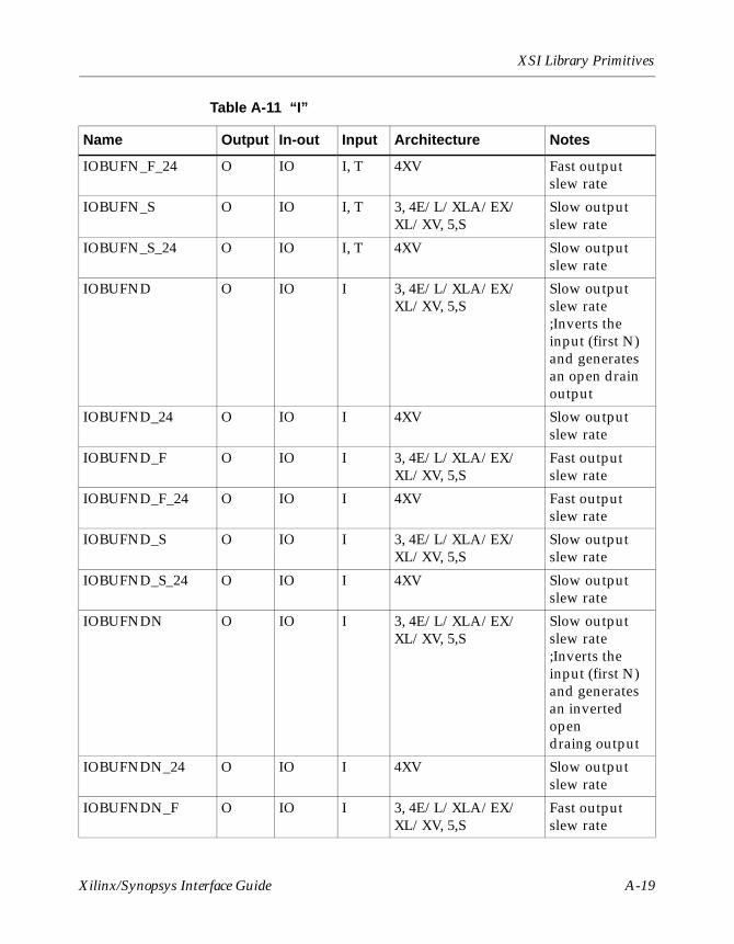
XSI Library Primitives
IOBUFN_F_24 O IO I, T 4XV Fast output slew rate
IOBUFN_S O IO I, T 3, 4E/L/XLA/EX/XL/XV, 5,S
Slow output slew rate
IOBUFN_S_24 O IO I, T 4XV Slow output slew rate
IOBUFND O IO I 3, 4E/L/XLA/EX/XL/XV, 5,S
Slow output slew rate;Inverts the input (first N) and generates an open drain output
IOBUFND_24 O IO I 4XV Slow output slew rate
IOBUFND_F O IO I 3, 4E/L/XLA/EX/XL/XV, 5,S
Fast output slew rate
IOBUFND_F_24 O IO I 4XV Fast output slew rate
IOBUFND_S O IO I 3, 4E/L/XLA/EX/XL/XV, 5,S
Slow output slew rate
IOBUFND_S_24 O IO I 4XV Slow output slew rate
IOBUFNDN O IO I 3, 4E/L/XLA/EX/XL/XV, 5,S
Slow output slew rate;Inverts the input (first N) and generates an inverted opendraing output
IOBUFNDN_24 O IO I 4XV Slow output slew rate
IOBUFNDN_F O IO I 3, 4E/L/XLA/EX/XL/XV, 5,S
Fast output slew rate
Table A-11 “I”
Name Output In-out Input Architecture Notes
Xilinx/Synopsys Interface Guide A-19
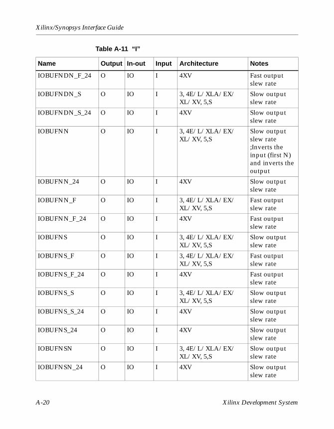
Xilinx/Synopsys Interface Guide
IOBUFNDN_F_24 O IO I 4XV Fast output slew rate
IOBUFNDN_S O IO I 3, 4E/L/XLA/EX/XL/XV, 5,S
Slow output slew rate
IOBUFNDN_S_24 O IO I 4XV Slow output slew rate
IOBUFNN O IO I 3, 4E/L/XLA/EX/XL/XV, 5,S
Slow output slew rate;Inverts the input (first N) and inverts the output
IOBUFNN_24 O IO I 4XV Slow output slew rate
IOBUFNN_F O IO I 3, 4E/L/XLA/EX/XL/XV, 5,S
Fast output slew rate
IOBUFNN_F_24 O IO I 4XV Fast output slew rate
IOBUFNS O IO I 3, 4E/L/XLA/EX/XL/XV, 5,S
Slow output slew rate
IOBUFNS_F O IO I 3, 4E/L/XLA/EX/XL/XV, 5,S
Fast output slew rate
IOBUFNS_F_24 O IO I 4XV Fast output slew rate
IOBUFNS_S O IO I 3, 4E/L/XLA/EX/XL/XV, 5,S
Slow output slew rate
IOBUFNS_S_24 O IO I 4XV Slow output slew rate
IOBUFNS_24 O IO I 4XV Slow output slew rate
IOBUFNSN O IO I 3, 4E/L/XLA/EX/XL/XV, 5,S
Slow output slew rate
IOBUFNSN_24 O IO I 4XV Slow output slew rate
Table A-11 “I”
Name Output In-out Input Architecture Notes
A-20 Xilinx Development System
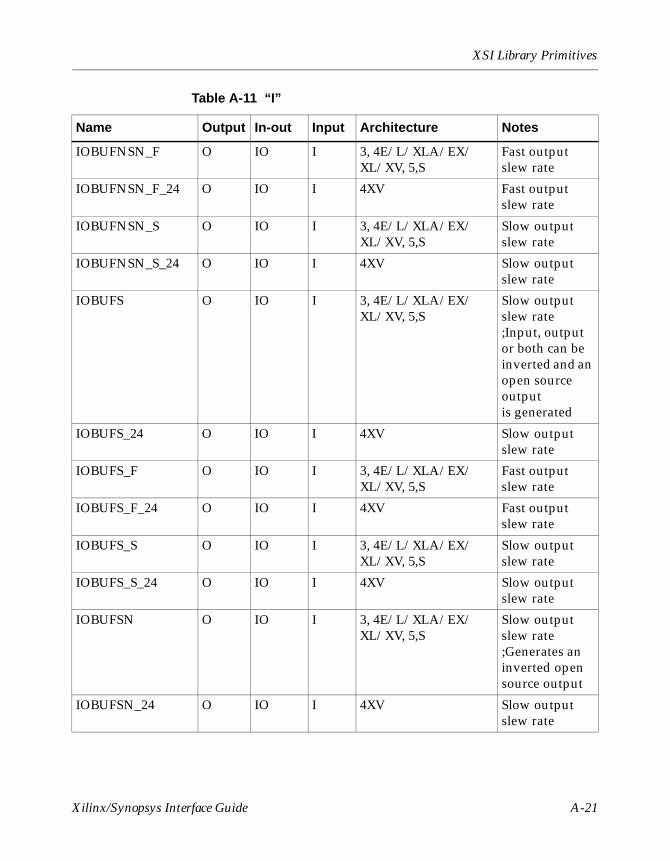
XSI Library Primitives
IOBUFNSN_F O IO I 3, 4E/L/XLA/EX/XL/XV, 5,S
Fast output slew rate
IOBUFNSN_F_24 O IO I 4XV Fast output slew rate
IOBUFNSN_S O IO I 3, 4E/L/XLA/EX/XL/XV, 5,S
Slow output slew rate
IOBUFNSN_S_24 O IO I 4XV Slow output slew rate
IOBUFS O IO I 3, 4E/L/XLA/EX/XL/XV, 5,S
Slow output slew rate;Input, output or both can be inverted and an open source outputis generated
IOBUFS_24 O IO I 4XV Slow output slew rate
IOBUFS_F O IO I 3, 4E/L/XLA/EX/XL/XV, 5,S
Fast output slew rate
IOBUFS_F_24 O IO I 4XV Fast output slew rate
IOBUFS_S O IO I 3, 4E/L/XLA/EX/XL/XV, 5,S
Slow output slew rate
IOBUFS_S_24 O IO I 4XV Slow output slew rate
IOBUFSN O IO I 3, 4E/L/XLA/EX/XL/XV, 5,S
Slow output slew rate;Generates an inverted open source output
IOBUFSN_24 O IO I 4XV Slow output slew rate
Table A-11 “I”
Name Output In-out Input Architecture Notes
Xilinx/Synopsys Interface Guide A-21
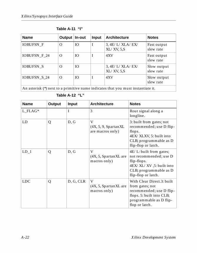
Xilinx/Synopsys Interface Guide
IOBUFSN_F O IO I 3, 4E/L/XLA/EX/XL/XV, 5,S
Fast output slew rate
IOBUFSN_F_24 O IO I 4XV Fast output slew rate
IOBUFSN_S O IO 3, 4E/L/XLA/EX/XL/XV, 5,S
Slow output slew rate
IOBUFSN_S_24 O IO I 4XV Slow output slew rate
An asterisk (*) next to a primitive name indicates that you must instantiate it.
Table A-12 “L”
Name Output Input Architecture Notes
L_FLAG* I 3 Rout signal along a longline.
LD Q D, G V(4X, 5, 9, SpartanXL are macros only)
3: built from gates; not recommended; use D flip-flops.4EX/XLXV, 5: built into CLB; programmable as D flip-flop or latch.
LD_1 Q D, G V(4X, 5, SpartanXL are macros only)
4E/L: built from gates; not recommended; use D flip-flops.4EX/XL/XV ,5: built into CLB; programmable as D flip-flop or latch.
LDC Q D, G, CLR V(4X, 5, SpartanXL are macros only)
With Clear Direct.3: built from gates; not recommended; use D flip-flops. 5: built into CLB; programmable as D flip-flop or latch.
Table A-11 “I”
Name Output In-out Input Architecture Notes
A-22 Xilinx Development System
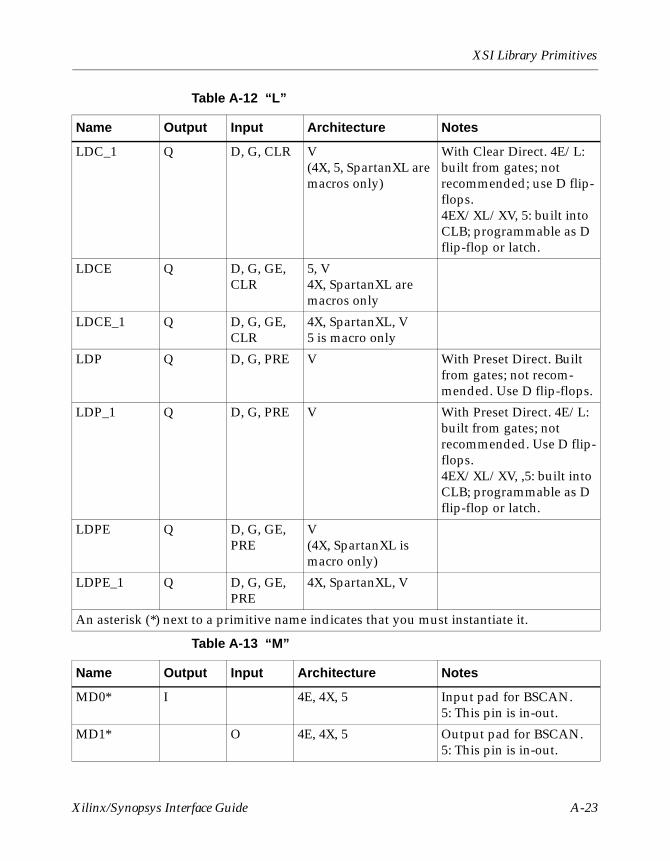
XSI Library Primitives
LDC_1 Q D, G, CLR V(4X, 5, SpartanXL are macros only)
With Clear Direct. 4E/L: built from gates; not recommended; use D flip-flops.4EX/XL/XV, 5: built into CLB; programmable as D flip-flop or latch.
LDCE Q D, G, GE, CLR
5, V4X, SpartanXL are macros only
LDCE_1 Q D, G, GE, CLR
4X, SpartanXL, V5 is macro only
LDP Q D, G, PRE V With Preset Direct. Built from gates; not recom-mended. Use D flip-flops.
LDP_1 Q D, G, PRE V With Preset Direct. 4E/L: built from gates; not recommended. Use D flip-flops.4EX/XL/XV, ,5: built into CLB; programmable as D flip-flop or latch.
LDPE Q D, G, GE, PRE
V(4X, SpartanXL is macro only)
LDPE_1 Q D, G, GE, PRE
4X, SpartanXL, V
An asterisk (*) next to a primitive name indicates that you must instantiate it.
Table A-13 “M”
Name Output Input Architecture Notes
MD0* I 4E, 4X, 5 Input pad for BSCAN.5: This pin is in-out.
MD1* O 4E, 4X, 5 Output pad for BSCAN.5: This pin is in-out.
Table A-12 “L”
Name Output Input Architecture Notes
Xilinx/Synopsys Interface Guide A-23
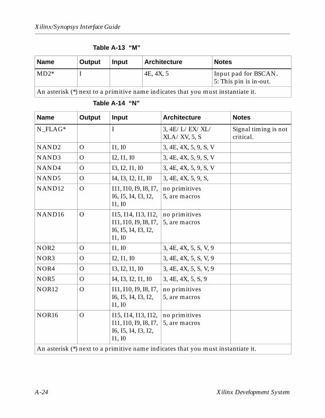
Xilinx/Synopsys Interface Guide
MD2* I 4E, 4X, 5 Input pad for BSCAN.5: This pin is in-out.
An asterisk (*) next to a primitive name indicates that you must instantiate it.
Table A-14 “N”
Name Output Input Architecture Notes
N_FLAG* I 3, 4E/L/EX/XL/XLA/XV, 5, S
Signal timing is not critical.
NAND2 O I1, I0 3, 4E, 4X, 5, 9, S, V
NAND3 O I2, I1, I0 3, 4E, 4X, 5, 9, S, V
NAND4 O I3, I2, I1, I0 3, 4E, 4X, 5, 9, S, V
NAND5 O I4, I3, I2, I1, I0 3, 4E, 4X, 5, 9, S,
NAND12 O I11, I10, I9, I8, I7, I6, I5, I4, I3, I2, I1, I0
no primitives5, are macros
NAND16 O I15, I14, I13, I12, I11, I10, I9, I8, I7, I6, I5, I4, I3, I2, I1, I0
no primitives5, are macros
NOR2 O I1, I0 3, 4E, 4X, 5, S, V, 9
NOR3 O I2, I1, I0 3, 4E, 4X, 5, S, V, 9
NOR4 O I3, I2, I1, I0 3, 4E, 4X, 5, S, V, 9
NOR5 O I4, I3, I2, I1, I0 3, 4E, 4X, 5, S, 9
NOR12 O I11, I10, I9, I8, I7, I6, I5, I4, I3, I2, I1, I0
no primitives5, are macros
NOR16 O I15, I14, I13, I12, I11, I10, I9, I8, I7, I6, I5, I4, I3, I2, I1, I0
no primitives5, are macros
An asterisk (*) next to a primitive name indicates that you must instantiate it.
Table A-13 “M”
Name Output Input Architecture Notes
A-24 Xilinx Development System
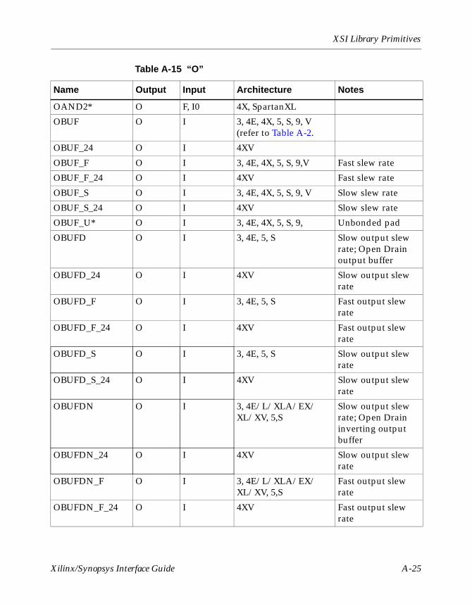
XSI Library Primitives
Table A-15 “O”
Name Output Input Architecture Notes
OAND2* O F, I0 4X, SpartanXL
OBUF O I 3, 4E, 4X, 5, S, 9, V (refer to Table A-2.
OBUF_24 O I 4XV
OBUF_F O I 3, 4E, 4X, 5, S, 9,V Fast slew rate
OBUF_F_24 O I 4XV Fast slew rate
OBUF_S O I 3, 4E, 4X, 5, S, 9, V Slow slew rate
OBUF_S_24 O I 4XV Slow slew rate
OBUF_U* O I 3, 4E, 4X, 5, S, 9, Unbonded pad
OBUFD O I 3, 4E, 5, S Slow output slew rate; Open Drain output buffer
OBUFD_24 O I 4XV Slow output slew rate
OBUFD_F O I 3, 4E, 5, S Fast output slew rate
OBUFD_F_24 O I 4XV Fast output slew rate
OBUFD_S O I 3, 4E, 5, S Slow output slew rate
OBUFD_S_24 O I 4XV Slow output slew rate
OBUFDN O I 3, 4E/L/XLA/EX/XL/XV, 5,S
Slow output slew rate; Open Drain inverting output buffer
OBUFDN_24 O I 4XV Slow output slew rate
OBUFDN_F O I 3, 4E/L/XLA/EX/XL/XV, 5,S
Fast output slew rate
OBUFDN_F_24 O I 4XV Fast output slew rate
Xilinx/Synopsys Interface Guide A-25
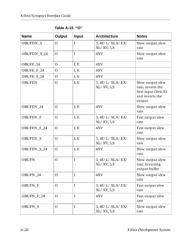
Xilinx/Synopsys Interface Guide
OBUFDN_S O I 3, 4E/L/XLA/EX/XL/XV, 5,S
Slow output slew rate
OBUFDN_S_24 O I 4XV Slow output slew rate
OBUFE_24 O I, E 4XV
OBUFE_F_24 O I, E 4XV
OBUFE_S_24 O I, E 4XV
OBUFEN O I, E 3, 4E/L/XLA/EX/XL/XV, 5,S
Slow output slew rate; inverts the first input (first E) and inverts the output
OBUFEN_24 O I, E 4XV Slow output slew rate
OBUFEN_F O I, E 3, 4E/L/XLA/EX/XL/XV, 5,S
Fast output slew rate
OBUFEN_F_24 O I, E 4XV Fast output slew rate
OBUFEN_S O I, E 3, 4E/L/XLA/EX/XL/XV, 5,S
Slow output slew rate
OBUFEN_S_24 O I, E 4XV Slow output slew rate
OBUFN O I 3, 4E/L/XLA/EX/XL/XV, 5,S
Slow output slew rate; Inverting output buffer
OBUFN_24 O I 4XV Slow output slew rate
OBUFN_F O I 3, 4E/L/XLA/EX/XL/XV, 5,S
Fast output slew rate
OBUFN_F_24 O I 4XV Fast output slew rate
OBUFN_S O I 3, 4E/L/XLA/EX/XL/XV, 5,S
Slow output slew rate
Table A-15 “O”
Name Output Input Architecture Notes
A-26 Xilinx Development System
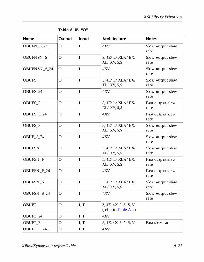
XSI Library Primitives
OBUFN_S_24 O I 4XV Slow output slew rate
OBUFNSN_S O I 3, 4E/L/XLA/EX/XL/XV, 5,S
Slow output slew rate
OBUFNSN_S_24 O I 4XV Slow output slew rate
OBUFS O I 3, 4E/L/XLA/EX/XL/XV, 5,S
Slow output slew rate
OBUFS_24 O I 4XV Slow output slew rate
OBUFS_F O I 3, 4E/L/XLA/EX/XL/XV, 5,S
Fast output slew rate
OBUFS_F_24 O I 4XV Fast output slew rate
OBUFS_S O I 3, 4E/L/XLA/EX/XL/XV, 5,S
Slow output slew rate
OBUF_S_24 O I 4XV Slow output slew rate
OBUFSN O I 3, 4E/L/XLA/EX/XL/XV, 5,S
Slow output slew rate
OBUFSN_F O I 3, 4E/L/XLA/EX/XL/XV, 5,S
Fast output slew rate
OBUFSN_F_24 O I 4XV Fast output slew rate
OBUFSN_S O I 3, 4E/L/XLA/EX/XL/XV, 5,S
Slow output slew rate
OBUFSN_S_24 O I 4XV Slow output slew rate
OBUFT O I, T 3, 4E, 4X, 9, 5, S, V (refer to Table A-2)
OBUFT_24 O I, T 4XV
OBUFT_F O I, T 3, 4E, 4X, 9, 5, S, V Fast slew rate
OBUFT_F_24 O I, T 4XV
Table A-15 “O”
Name Output Input Architecture Notes
Xilinx/Synopsys Interface Guide A-27
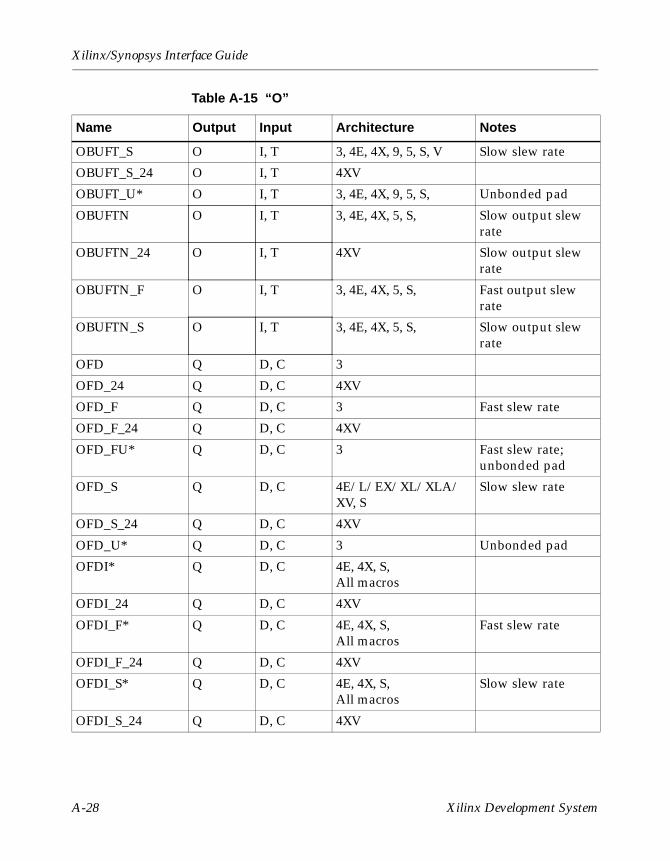
Xilinx/Synopsys Interface Guide
OBUFT_S O I, T 3, 4E, 4X, 9, 5, S, V Slow slew rate
OBUFT_S_24 O I, T 4XV
OBUFT_U* O I, T 3, 4E, 4X, 9, 5, S, Unbonded pad
OBUFTN O I, T 3, 4E, 4X, 5, S, Slow output slew rate
OBUFTN_24 O I, T 4XV Slow output slew rate
OBUFTN_F O I, T 3, 4E, 4X, 5, S, Fast output slew rate
OBUFTN_S O I, T 3, 4E, 4X, 5, S, Slow output slew rate
OFD Q D, C 3
OFD_24 Q D, C 4XV
OFD_F Q D, C 3 Fast slew rate
OFD_F_24 Q D, C 4XV
OFD_FU* Q D, C 3 Fast slew rate; unbonded pad
OFD_S Q D, C 4E/L/EX/XL/XLA/XV, S
Slow slew rate
OFD_S_24 Q D, C 4XV
OFD_U* Q D, C 3 Unbonded pad
OFDI* Q D, C 4E, 4X, S, All macros
OFDI_24 Q D, C 4XV
OFDI_F* Q D, C 4E, 4X, S, All macros
Fast slew rate
OFDI_F_24 Q D, C 4XV
OFDI_S* Q D, C 4E, 4X, S, All macros
Slow slew rate
OFDI_S_24 Q D, C 4XV
Table A-15 “O”
Name Output Input Architecture Notes
A-28 Xilinx Development System
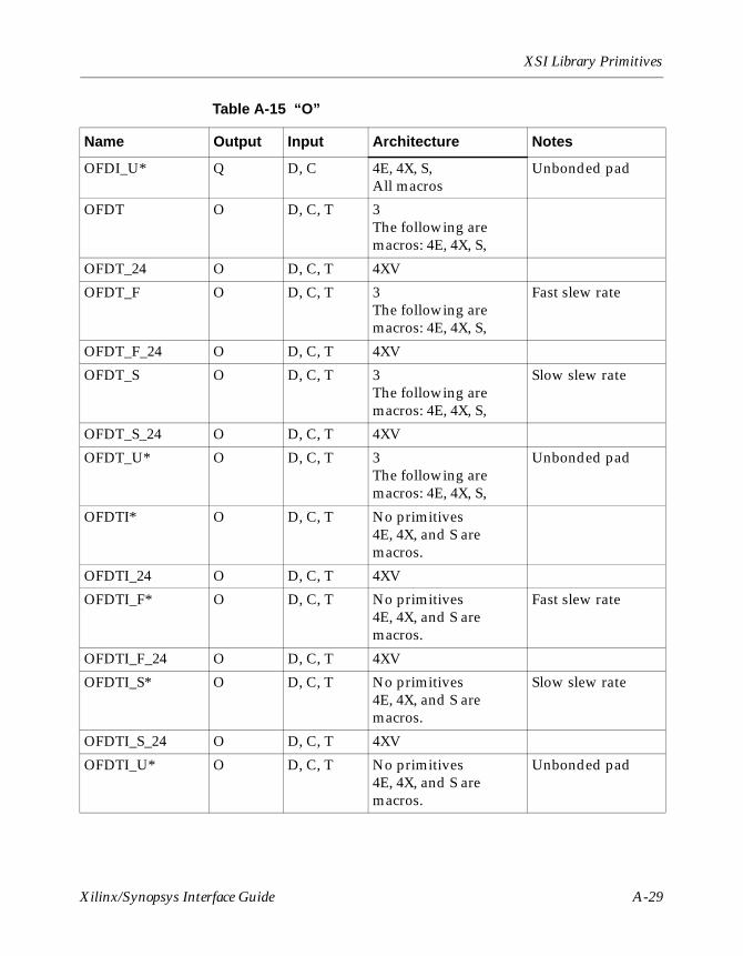
XSI Library Primitives
OFDI_U* Q D, C 4E, 4X, S, All macros
Unbonded pad
OFDT O D, C, T 3The following are macros: 4E, 4X, S,
OFDT_24 O D, C, T 4XV
OFDT_F O D, C, T 3The following are macros: 4E, 4X, S,
Fast slew rate
OFDT_F_24 O D, C, T 4XV
OFDT_S O D, C, T 3The following are macros: 4E, 4X, S,
Slow slew rate
OFDT_S_24 O D, C, T 4XV
OFDT_U* O D, C, T 3The following are macros: 4E, 4X, S,
Unbonded pad
OFDTI* O D, C, T No primitives4E, 4X, and S are macros.
OFDTI_24 O D, C, T 4XV
OFDTI_F* O D, C, T No primitives4E, 4X, and S are macros.
Fast slew rate
OFDTI_F_24 O D, C, T 4XV
OFDTI_S* O D, C, T No primitives4E, 4X, and S are macros.
Slow slew rate
OFDTI_S_24 O D, C, T 4XV
OFDTI_U* O D, C, T No primitives4E, 4X, and S are macros.
Unbonded pad
Table A-15 “O”
Name Output Input Architecture Notes
Xilinx/Synopsys Interface Guide A-29
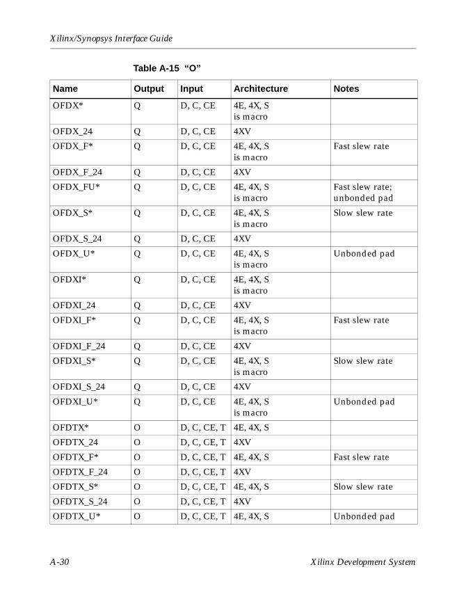
Xilinx/Synopsys Interface Guide
OFDX* Q D, C, CE 4E, 4X, Sis macro
OFDX_24 Q D, C, CE 4XV
OFDX_F* Q D, C, CE 4E, 4X, Sis macro
Fast slew rate
OFDX_F_24 Q D, C, CE 4XV
OFDX_FU* Q D, C, CE 4E, 4X, Sis macro
Fast slew rate; unbonded pad
OFDX_S* Q D, C, CE 4E, 4X, Sis macro
Slow slew rate
OFDX_S_24 Q D, C, CE 4XV
OFDX_U* Q D, C, CE 4E, 4X, Sis macro
Unbonded pad
OFDXI* Q D, C, CE 4E, 4X, Sis macro
OFDXI_24 Q D, C, CE 4XV
OFDXI_F* Q D, C, CE 4E, 4X, Sis macro
Fast slew rate
OFDXI_F_24 Q D, C, CE 4XV
OFDXI_S* Q D, C, CE 4E, 4X, Sis macro
Slow slew rate
OFDXI_S_24 Q D, C, CE 4XV
OFDXI_U* Q D, C, CE 4E, 4X, Sis macro
Unbonded pad
OFDTX* O D, C, CE, T 4E, 4X, S
OFDTX_24 O D, C, CE, T 4XV
OFDTX_F* O D, C, CE, T 4E, 4X, S Fast slew rate
OFDTX_F_24 O D, C, CE, T 4XV
OFDTX_S* O D, C, CE, T 4E, 4X, S Slow slew rate
OFDTX_S_24 O D, C, CE, T 4XV
OFDTX_U* O D, C, CE, T 4E, 4X, S Unbonded pad
Table A-15 “O”
Name Output Input Architecture Notes
A-30 Xilinx Development System
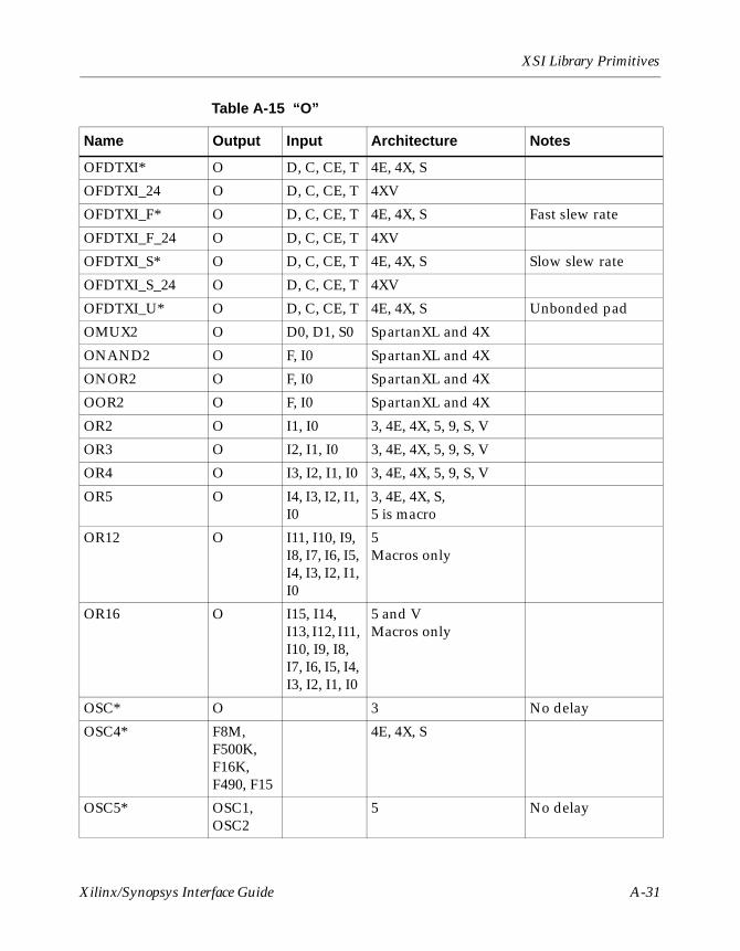
XSI Library Primitives
OFDTXI* O D, C, CE, T 4E, 4X, S
OFDTXI_24 O D, C, CE, T 4XV
OFDTXI_F* O D, C, CE, T 4E, 4X, S Fast slew rate
OFDTXI_F_24 O D, C, CE, T 4XV
OFDTXI_S* O D, C, CE, T 4E, 4X, S Slow slew rate
OFDTXI_S_24 O D, C, CE, T 4XV
OFDTXI_U* O D, C, CE, T 4E, 4X, S Unbonded pad
OMUX2 O D0, D1, S0 SpartanXL and 4X
ONAND2 O F, I0 SpartanXL and 4X
ONOR2 O F, I0 SpartanXL and 4X
OOR2 O F, I0 SpartanXL and 4X
OR2 O I1, I0 3, 4E, 4X, 5, 9, S, V
OR3 O I2, I1, I0 3, 4E, 4X, 5, 9, S, V
OR4 O I3, I2, I1, I0 3, 4E, 4X, 5, 9, S, V
OR5 O I4, I3, I2, I1, I0
3, 4E, 4X, S, 5 is macro
OR12 O I11, I10, I9, I8, I7, I6, I5, I4, I3, I2, I1, I0
5 Macros only
OR16 O I15, I14, I13, I12, I11, I10, I9, I8, I7, I6, I5, I4, I3, I2, I1, I0
5 and VMacros only
OSC* O 3 No delay
OSC4* F8M, F500K, F16K, F490, F15
4E, 4X, S
OSC5* OSC1, OSC2
5 No delay
Table A-15 “O”
Name Output Input Architecture Notes
Xilinx/Synopsys Interface Guide A-31
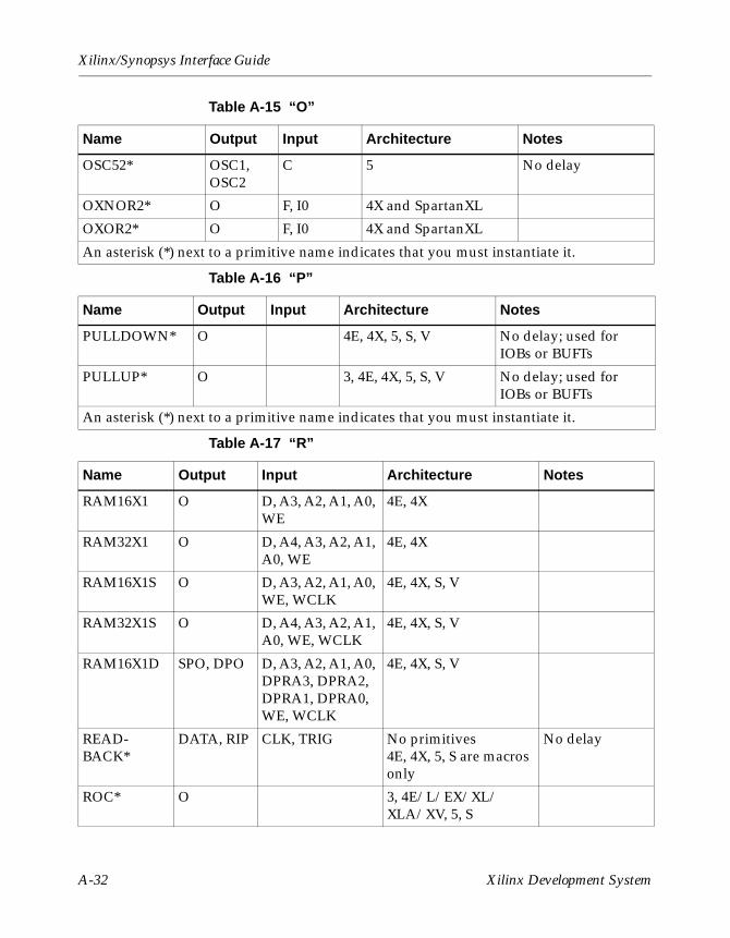
Xilinx/Synopsys Interface Guide
OSC52* OSC1, OSC2
C 5 No delay
OXNOR2* O F, I0 4X and SpartanXL
OXOR2* O F, I0 4X and SpartanXL
An asterisk (*) next to a primitive name indicates that you must instantiate it.
Table A-16 “P”
Name Output Input Architecture Notes
PULLDOWN* O 4E, 4X, 5, S, V No delay; used for IOBs or BUFTs
PULLUP* O 3, 4E, 4X, 5, S, V No delay; used for IOBs or BUFTs
An asterisk (*) next to a primitive name indicates that you must instantiate it.
Table A-17 “R”
Name Output Input Architecture Notes
RAM16X1 O D, A3, A2, A1, A0, WE
4E, 4X
RAM32X1 O D, A4, A3, A2, A1, A0, WE
4E, 4X
RAM16X1S O D, A3, A2, A1, A0, WE, WCLK
4E, 4X, S, V
RAM32X1S O D, A4, A3, A2, A1, A0, WE, WCLK
4E, 4X, S, V
RAM16X1D SPO, DPO D, A3, A2, A1, A0, DPRA3, DPRA2, DPRA1, DPRA0, WE, WCLK
4E, 4X, S, V
READ-BACK*
DATA, RIP CLK, TRIG No primitives4E, 4X, 5, S are macros only
No delay
ROC* O 3, 4E/L/EX/XL/XLA/XV, 5, S
Table A-15 “O”
Name Output Input Architecture Notes
A-32 Xilinx Development System
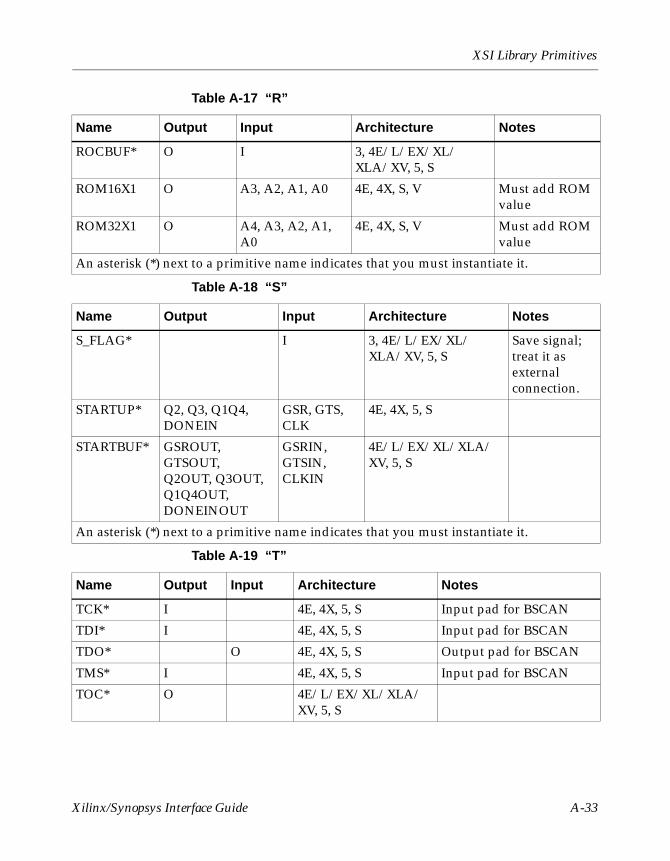
XSI Library Primitives
ROCBUF* O I 3, 4E/L/EX/XL/XLA/XV, 5, S
ROM16X1 O A3, A2, A1, A0 4E, 4X, S, V Must add ROM value
ROM32X1 O A4, A3, A2, A1, A0
4E, 4X, S, V Must add ROM value
An asterisk (*) next to a primitive name indicates that you must instantiate it.
Table A-18 “S”
Name Output Input Architecture Notes
S_FLAG* I 3, 4E/L/EX/XL/XLA/XV, 5, S
Save signal; treat it as external connection.
STARTUP* Q2, Q3, Q1Q4, DONEIN
GSR, GTS, CLK
4E, 4X, 5, S
STARTBUF* GSROUT, GTSOUT,Q2OUT, Q3OUT, Q1Q4OUT, DONEINOUT
GSRIN, GTSIN, CLKIN
4E/L/EX/XL/XLA/XV, 5, S
An asterisk (*) next to a primitive name indicates that you must instantiate it.
Table A-19 “T”
Name Output Input Architecture Notes
TCK* I 4E, 4X, 5, S Input pad for BSCAN
TDI* I 4E, 4X, 5, S Input pad for BSCAN
TDO* O 4E, 4X, 5, S Output pad for BSCAN
TMS* I 4E, 4X, 5, S Input pad for BSCAN
TOC* O 4E/L/EX/XL/XLA/XV, 5, S
Table A-17 “R”
Name Output Input Architecture Notes
Xilinx/Synopsys Interface Guide A-33
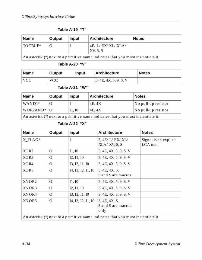
Xilinx/Synopsys Interface Guide
TOCBUF* O I 4E/L/EX/XL/XLA/XV, 5, S
An asterisk (*) next to a primitive name indicates that you must instantiate it.
Table A-20 “V”
Name Output Input Architecture Notes
VCC VCC 3, 4E, 4X, 5, 9, S, V
Table A-21 “W”
Name Output Input Architecture Notes
WAND1* O I 4E, 4X No pull-up resistor
WOR2AND* O I1, I0 4E, 4X No pull-up resistor
An asterisk (*) next to a primitive name indicates that you must instantiate it.
Table A-22 “X”
Name Output Input Architecture Notes
X_FLAG* I 3, 4E/L/EX/XL/XLA/XV, 5, S
Signal is an explicit LCA net.
XOR2 O I1, I0 3, 4E, 4X, 5, 9, S, V
XOR3 O I2, I1, I0 3, 4E, 4X, 5, 9, S, V
XOR4 O I3, I2, I1, I0 3, 4E, 4X, 5, 9, S, V
XOR5 O I4, I3, I2, I1, I0 3, 4E, 4X, S, 5 and 9 are macros
XNOR2 O I1, I0 3, 4E, 4X, 5, 9, S, V
XNOR3 O I2, I1, I0 3, 4E, 4X, 5, 9, S, V
XNOR4 O I3, I2, I1, I0 3, 4E, 4X, 5, 9, S, V
XNOR5 O I4, I3, I2, I1, I0 3, 4E, 4X, S, 5 and 9 are macros only
An asterisk (*) next to a primitive name indicates that you must instantiate it.
Table A-19 “T”
Name Output Input Architecture Notes
A-34 Xilinx Development System
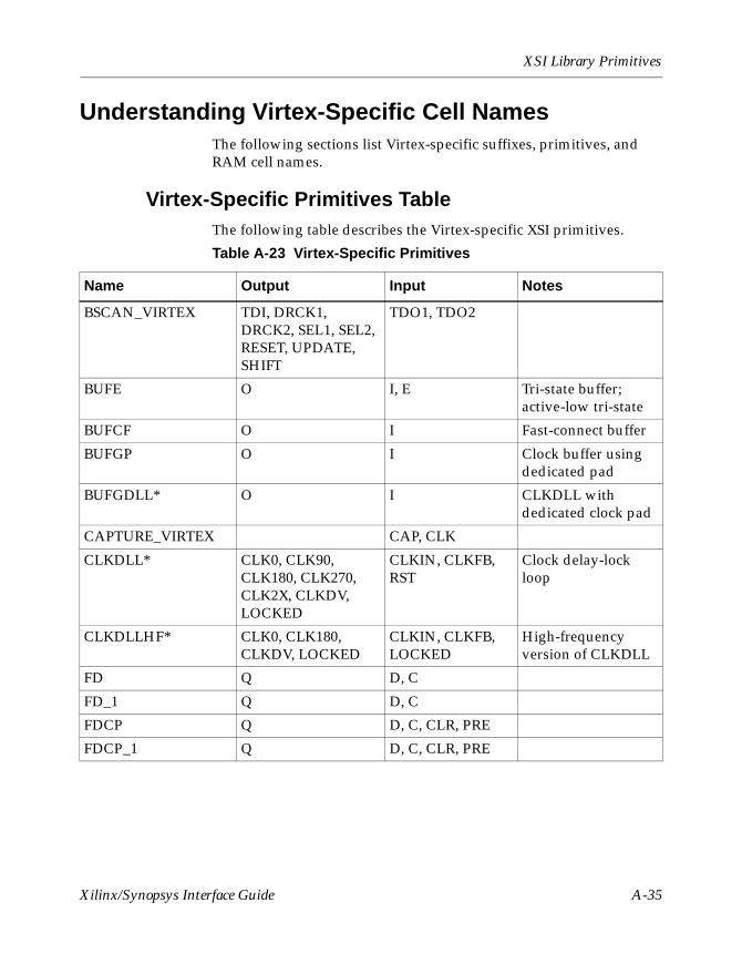
XSI Library Primitives
Understanding Virtex-Specific Cell NamesThe following sections list Virtex-specific suffixes, primitives, and RAM cell names.
Virtex-Specific Primitives TableThe following table describes the Virtex-specific XSI primitives.
Table A-23 Virtex-Specific Primitives
Name Output Input Notes
BSCAN_VIRTEX TDI, DRCK1, DRCK2, SEL1, SEL2, RESET, UPDATE, SHIFT
TDO1, TDO2
BUFE O I, E Tri-state buffer; active-low tri-state
BUFCF O I Fast-connect buffer
BUFGP O I Clock buffer using dedicated pad
BUFGDLL* O I CLKDLL with dedicated clock pad
CAPTURE_VIRTEX CAP, CLK
CLKDLL* CLK0, CLK90, CLK180, CLK270, CLK2X, CLKDV, LOCKED
CLKIN, CLKFB, RST
Clock delay-lock loop
CLKDLLHF* CLK0, CLK180, CLKDV, LOCKED
CLKIN, CLKFB, LOCKED
High-frequency version of CLKDLL
FD Q D, C
FD_1 Q D, C
FDCP Q D, C, CLR, PRE
FDCP_1 Q D, C, CLR, PRE
Xilinx/Synopsys Interface Guide A-35
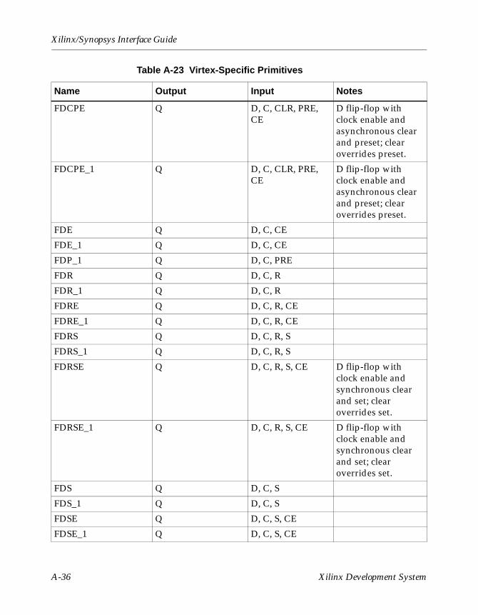
Xilinx/Synopsys Interface Guide
FDCPE Q D, C, CLR, PRE, CE
D flip-flop with clock enable and asynchronous clear and preset; clear overrides preset.
FDCPE_1 Q D, C, CLR, PRE, CE
D flip-flop with clock enable and asynchronous clear and preset; clear overrides preset.
FDE Q D, C, CE
FDE_1 Q D, C, CE
FDP_1 Q D, C, PRE
FDR Q D, C, R
FDR_1 Q D, C, R
FDRE Q D, C, R, CE
FDRE_1 Q D, C, R, CE
FDRS Q D, C, R, S
FDRS_1 Q D, C, R, S
FDRSE Q D, C, R, S, CE D flip-flop with clock enable and synchronous clear and set; clear overrides set.
FDRSE_1 Q D, C, R, S, CE D flip-flop with clock enable and synchronous clear and set; clear overrides set.
FDS Q D, C, S
FDS_1 Q D, C, S
FDSE Q D, C, S, CE
FDSE_1 Q D, C, S, CE
Table A-23 Virtex-Specific Primitives
Name Output Input Notes
A-36 Xilinx Development System
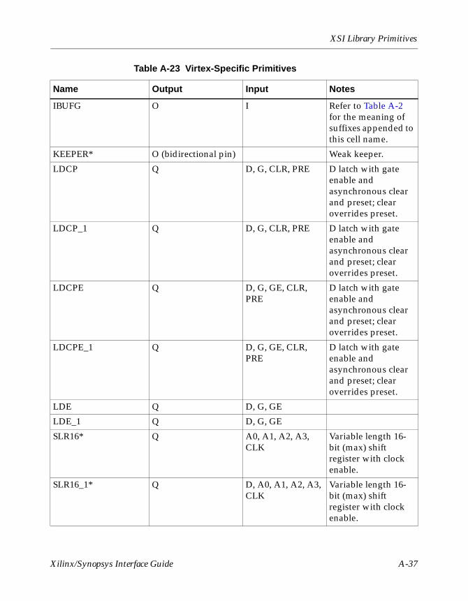
XSI Library Primitives
IBUFG O I Refer to Table A-2 for the meaning of suffixes appended to this cell name.
KEEPER* O (bidirectional pin) Weak keeper.
LDCP Q D, G, CLR, PRE D latch with gate enable and asynchronous clear and preset; clear overrides preset.
LDCP_1 Q D, G, CLR, PRE D latch with gate enable and asynchronous clear and preset; clear overrides preset.
LDCPE Q D, G, GE, CLR, PRE
D latch with gate enable and asynchronous clear and preset; clear overrides preset.
LDCPE_1 Q D, G, GE, CLR, PRE
D latch with gate enable and asynchronous clear and preset; clear overrides preset.
LDE Q D, G, GE
LDE_1 Q D, G, GE
SLR16* Q A0, A1, A2, A3, CLK
Variable length 16-bit (max) shift register with clock enable.
SLR16_1* Q D, A0, A1, A2, A3, CLK
Variable length 16-bit (max) shift register with clock enable.
Table A-23 Virtex-Specific Primitives
Name Output Input Notes
Xilinx/Synopsys Interface Guide A-37
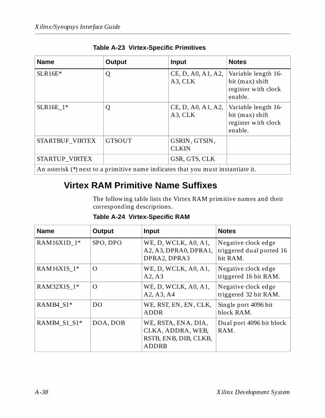
Xilinx/Synopsys Interface Guide
Virtex RAM Primitive Name SuffixesThe following table lists the Virtex RAM primitive names and their corresponding descriptions.
SLR16E* Q CE, D, A0, A1, A2, A3, CLK
Variable length 16-bit (max) shift register with clock enable.
SLR16E_1* Q CE, D, A0, A1, A2, A3, CLK
Variable length 16-bit (max) shift register with clock enable.
STARTBUF_VIRTEX GTSOUT GSRIN, GTSIN, CLKIN
STARTUP_VIRTEX GSR, GTS, CLK
An asterisk (*) next to a primitive name indicates that you must instantiate it.
Table A-24 Virtex-Specific RAM
Name Output Input Notes
RAM16X1D_1* SPO, DPO WE, D, WCLK, A0, A1, A2, A3, DPRA0, DPRA1, DPRA2, DPRA3
Negative clock edge triggered dual ported 16 bit RAM.
RAM16X1S_1* O WE, D, WCLK, A0, A1, A2, A3
Negative clock edge triggered 16 bit RAM.
RAM32X1S_1* O WE, D, WCLK, A0, A1, A2, A3, A4
Negative clock edge triggered 32 bit RAM.
RAMB4_S1* DO WE, RST, EN, EN, CLK, ADDR
Single port 4096 bit block RAM.
RAMB4_S1_S1* DOA, DOB WE, RSTA, ENA, DIA, CLKA, ADDRA, WEB, RSTB, ENB, DIB, CLKB, ADDRB
Dual port 4096 bit block RAM.
Table A-23 Virtex-Specific Primitives
Name Output Input Notes
A-38 Xilinx Development System
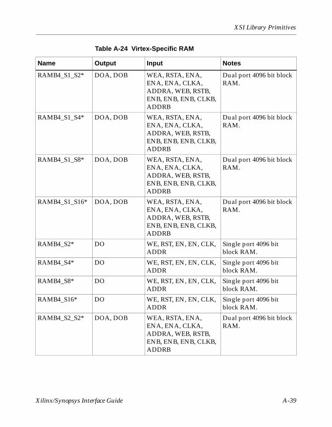
XSI Library Primitives
RAMB4_S1_S2* DOA, DOB WEA, RSTA, ENA, ENA, ENA, CLKA, ADDRA, WEB, RSTB, ENB, ENB, ENB, CLKB, ADDRB
Dual port 4096 bit block RAM.
RAMB4_S1_S4* DOA, DOB WEA, RSTA, ENA, ENA, ENA, CLKA, ADDRA, WEB, RSTB, ENB, ENB, ENB, CLKB, ADDRB
Dual port 4096 bit block RAM.
RAMB4_S1_S8* DOA, DOB WEA, RSTA, ENA, ENA, ENA, CLKA, ADDRA, WEB, RSTB, ENB, ENB, ENB, CLKB, ADDRB
Dual port 4096 bit block RAM.
RAMB4_S1_S16* DOA, DOB WEA, RSTA, ENA, ENA, ENA, CLKA, ADDRA, WEB, RSTB, ENB, ENB, ENB, CLKB, ADDRB
Dual port 4096 bit block RAM.
RAMB4_S2* DO WE, RST, EN, EN, CLK, ADDR
Single port 4096 bit block RAM.
RAMB4_S4* DO WE, RST, EN, EN, CLK, ADDR
Single port 4096 bit block RAM.
RAMB4_S8* DO WE, RST, EN, EN, CLK, ADDR
Single port 4096 bit block RAM.
RAMB4_S16* DO WE, RST, EN, EN, CLK, ADDR
Single port 4096 bit block RAM.
RAMB4_S2_S2* DOA, DOB WEA, RSTA, ENA, ENA, ENA, CLKA, ADDRA, WEB, RSTB, ENB, ENB, ENB, CLKB, ADDRB
Dual port 4096 bit block RAM.
Table A-24 Virtex-Specific RAM
Name Output Input Notes
Xilinx/Synopsys Interface Guide A-39
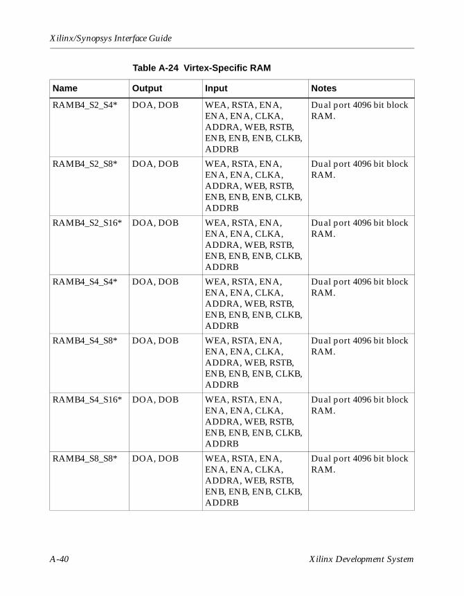
Xilinx/Synopsys Interface Guide
RAMB4_S2_S4* DOA, DOB WEA, RSTA, ENA, ENA, ENA, CLKA, ADDRA, WEB, RSTB, ENB, ENB, ENB, CLKB, ADDRB
Dual port 4096 bit block RAM.
RAMB4_S2_S8* DOA, DOB WEA, RSTA, ENA, ENA, ENA, CLKA, ADDRA, WEB, RSTB, ENB, ENB, ENB, CLKB, ADDRB
Dual port 4096 bit block RAM.
RAMB4_S2_S16* DOA, DOB WEA, RSTA, ENA, ENA, ENA, CLKA, ADDRA, WEB, RSTB, ENB, ENB, ENB, CLKB, ADDRB
Dual port 4096 bit block RAM.
RAMB4_S4_S4* DOA, DOB WEA, RSTA, ENA, ENA, ENA, CLKA, ADDRA, WEB, RSTB, ENB, ENB, ENB, CLKB, ADDRB
Dual port 4096 bit block RAM.
RAMB4_S4_S8* DOA, DOB WEA, RSTA, ENA, ENA, ENA, CLKA, ADDRA, WEB, RSTB, ENB, ENB, ENB, CLKB, ADDRB
Dual port 4096 bit block RAM.
RAMB4_S4_S16* DOA, DOB WEA, RSTA, ENA, ENA, ENA, CLKA, ADDRA, WEB, RSTB, ENB, ENB, ENB, CLKB, ADDRB
Dual port 4096 bit block RAM.
RAMB4_S8_S8* DOA, DOB WEA, RSTA, ENA, ENA, ENA, CLKA, ADDRA, WEB, RSTB, ENB, ENB, ENB, CLKB, ADDRB
Dual port 4096 bit block RAM.
Table A-24 Virtex-Specific RAM
Name Output Input Notes
A-40 Xilinx Development System
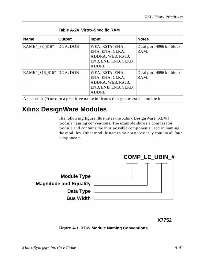
XSI Library Primitives
Xilinx DesignWare ModulesThe following figure illustrates the Xilinx DesignWare (XDW) module naming conventions. The example shows a comparator module and contains the four possible components used in naming the modules. Other module names do not necessarily contain all four components.
Figure A-1 XDW Module Naming Conventions
RAMB4_S8_S16* DOA, DOB WEA, RSTA, ENA, ENA, ENA, CLKA, ADDRA, WEB, RSTB, ENB, ENB, ENB, CLKB, ADDRB
Dual port 4096 bit block RAM.
RAMB4_S16_S16* DOA, DOB WEA, RSTA, ENA, ENA, ENA, CLKA, ADDRA, WEB, RSTB, ENB, ENB, ENB, CLKB, ADDRB
Dual port 4096 bit block RAM.
An asterisk (*) next to a primitive name indicates that you must instantiate it.
Table A-24 Virtex-Specific RAM
Name Output Input Notes
COMP_LE_UBIN_#
Module Type
Magnitude and Equality
Data TypeBus Width
X7752
Xilinx/Synopsys Interface Guide A-41
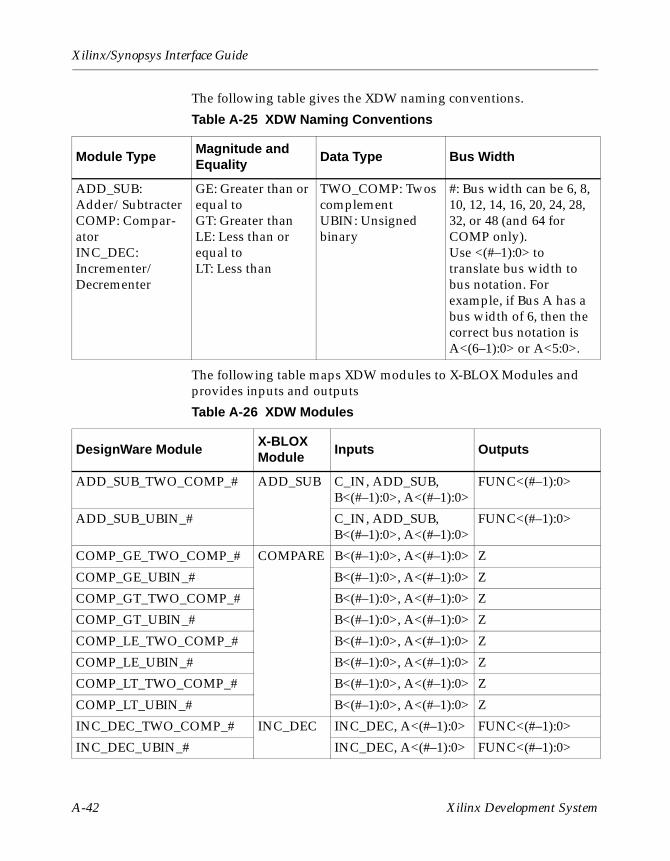
Xilinx/Synopsys Interface Guide
The following table gives the XDW naming conventions.
The following table maps XDW modules to X-BLOX Modules and provides inputs and outputs
Table A-25 XDW Naming Conventions
Module TypeMagnitude and Equality
Data Type Bus Width
ADD_SUB: Adder/SubtracterCOMP: Compar-atorINC_DEC:Incrementer/Decrementer
GE: Greater than or equal toGT: Greater thanLE: Less than or equal toLT: Less than
TWO_COMP: Twos complementUBIN: Unsigned binary
#: Bus width can be 6, 8, 10, 12, 14, 16, 20, 24, 28, 32, or 48 (and 64 for COMP only).Use <(#–1):0> to translate bus width to bus notation. For example, if Bus A has a bus width of 6, then the correct bus notation is A<(6–1):0> or A<5:0>.
Table A-26 XDW Modules
DesignWare ModuleX-BLOX Module
Inputs Outputs
ADD_SUB_TWO_COMP_# ADD_SUB C_IN, ADD_SUB, B<(#–1):0>, A<(#–1):0>
FUNC<(#–1):0>
ADD_SUB_UBIN_# C_IN, ADD_SUB, B<(#–1):0>, A<(#–1):0>
FUNC<(#–1):0>
COMP_GE_TWO_COMP_# COMPARE B<(#–1):0>, A<(#–1):0> Z
COMP_GE_UBIN_# B<(#–1):0>, A<(#–1):0> Z
COMP_GT_TWO_COMP_# B<(#–1):0>, A<(#–1):0> Z
COMP_GT_UBIN_# B<(#–1):0>, A<(#–1):0> Z
COMP_LE_TWO_COMP_# B<(#–1):0>, A<(#–1):0> Z
COMP_LE_UBIN_# B<(#–1):0>, A<(#–1):0> Z
COMP_LT_TWO_COMP_# B<(#–1):0>, A<(#–1):0> Z
COMP_LT_UBIN_# B<(#–1):0>, A<(#–1):0> Z
INC_DEC_TWO_COMP_# INC_DEC INC_DEC, A<(#–1):0> FUNC<(#–1):0>
INC_DEC_UBIN_# INC_DEC, A<(#–1):0> FUNC<(#–1):0>
A-42 Xilinx Development System
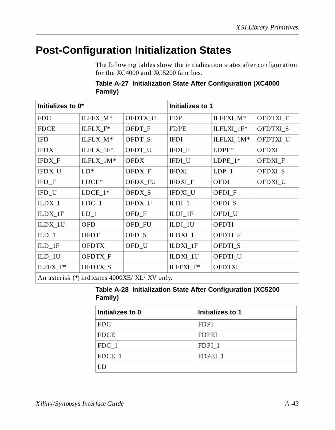
XSI Library Primitives
Post-Configuration Initialization StatesThe following tables show the initialization states after configuration for the XC4000 and XC5200 families.
Table A-27 Initialization State After Configuration (XC4000 Family)
Initializes to 0* Initializes to 1
FDC ILFFX_M* OFDTX_U FDP ILFFXI_M* OFDTXI_F
FDCE ILFLX_F* OFDT_F FDPE ILFLXI_1F* OFDTXI_S
IFD ILFLX_M* OFDT_S IFDI ILFLXI_1M* OFDTXI_U
IFDX ILFLX_1F* OFDT_U IFDI_F LDPE* OFDXI
IFDX_F ILFLX_1M* OFDX IFDI_U LDPE_1* OFDXI_F
IFDX_U LD* OFDX_F IFDXI LDP_1 OFDXI_S
IFD_F LDCE* OFDX_FU IFDXI_F OFDI OFDXI_U
IFD_U LDCE_1* OFDX_S IFDXI_U OFDI_F
ILDX_1 LDC_1 OFDX_U ILDI_1 OFDI_S
ILDX_1F LD_1 OFD_F ILDI_1F OFDI_U
ILDX_1U OFD OFD_FU ILDI_1U OFDTI
ILD_1 OFDT OFD_S ILDXI_1 OFDTI_F
ILD_1F OFDTX OFD_U ILDXI_1F OFDTI_S
ILD_1U OFDTX_F ILDXI_1U OFDTI_U
ILFFX_F* OFDTX_S ILFFXI_F* OFDTXI
An asterisk (*) indicates 4000XE/XL/XV only.
Table A-28 Initialization State After Configuration (XC5200 Family)
Initializes to 0 Initializes to 1
FDC FDPI
FDCE FDPEI
FDC_1 FDPI_1
FDCE_1 FDPEI_1
LD
Xilinx/Synopsys Interface Guide A-43
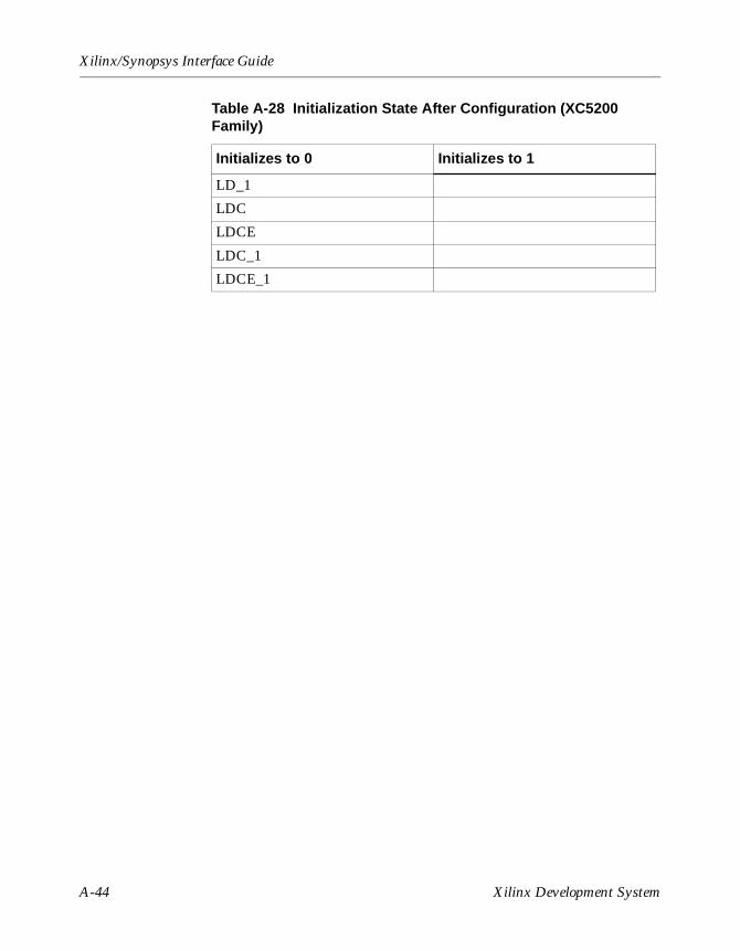
Xilinx/Synopsys Interface Guide
LD_1
LDC
LDCE
LDC_1
LDCE_1
Table A-28 Initialization State After Configuration (XC5200 Family)
Initializes to 0 Initializes to 1
A-44 Xilinx Development System
Appendix B
Targeting Virtex Devices
Generally, you target a Virtex device no differently than the way you target a non-Virtex device. However, you use Virtex-specific settings, such as .synopsys_dc.setup options, that only apply to Virtex. This appendix outlines only the major differences you encounter when targeting a Virtex device. For topics not covered here, equivalent instructions for a non-Virtex device apply and those instructions exist earlier in this manual.
Unless otherwise specified, all references to FPGA Compiler also apply to Design Compiler.
This appendix contains the following topics.
• “Following General Guidelines.”
• “Setting FPGA Compiler to Synthesize a Virtex Design”
• “Synthesizing a Virtex Design into FPGA Compiler”
• “Setting VSS Simulation for Virtex”
• “Setting FPGA Compiler II for Virtex”
• “Synthesizing a Virtex Design in FPGA Compiler II”
• “Using Clock Delay Locked Loops with Synopsys”
Following General GuidelinesUse these following general guidelines when targeting Virtex devices.
Virtex XSI uses an EDIF-based synthesis flow with FPGA Compiler and FPGA Compiler II.
Xilinx/Synopsys Interface Guide B-1
Xilinx/Synopsys Interface Guide
For I/O cells with a specific type of input delay and current drive in the FPGA Compiler flow, instantiate the desired IBUF, OBUF, IFD, and other primitives. Refer to the “XSI Library Primitives” appendix for the exact I/O library cell name and pin names. For I/O cells in FPGA Compiler II, you can infer the desired type of input delay, pull-up or pull-down, and current drive using the FPGA Compiler II implementation GUI.
Do not use the Ungroup –all –flatten command when synthesizing a Virtex design with FPGA Compiler.
A software bug exists in the DesignWare Compiler that causes the uniquify command to remove attributes from library cells. The result is a LUT primitive with no attributes defining how the LUT works. The resulting netlist will error out during the NGDBuild process. Compile all lower level modules. Place a dont_touch attribute on the complied modules, then compile the top level module. Do not set the Synopsys variable hdlin_replace_synthetic=true to expand the operators while reading in the HDL design code. Doing so can result in less-than-optimal designs, because the compiler cannot make appropriate trade-offs. Do not use the replace_fpga command for virtex flows. The replace_fpga command will replace the LUTs in the netlist with primitive gates.
Use the following commands for the set_dont_touch attribute.
current_design alu compile -map_effort \
[low|medium|high] \
set_dont_touch alu \
current_design top compile -map_effort \
[low|medium|high]
You can use two types of simulation when simulating a Virtex design with either Verilog or VHDL; RTL simulation and post-NGDbuild simulation.
Setting FPGA Compiler to Synthesize a Virtex Design
Use the following procedure to set FPGA Compiler for Virtex design simulation.
1. Set your Xilinx and Synopsys software environments.
B-2 Xilinx Development System
Targeting Virtex Devices
For instructions about setting up this current release of Xilinx software, please refer to the ISE 4 Release Notes. For instructions about setting up Synopsys products, refer to the Synopsys installation guide.
2. Copy the file $XILINX/synopsys/examples/template.synopsys_dc.setup_fc into a directory.
3. Run synlibs to get the correct synthesis libraries into the .synopsys_dc.setup file. Execute the following command in the same directory that contains the .synopsys_dc.setup file for Virtex.
synlibs xfpga_virtex-3>>.synopsys_dc.setup
4. Check that your system administrator compiled the XDW ISE 4 XSI libraries.
By default, these DesignWare libraries are compiled for Synopsys v1999.05. If using a version of Synopsys newer than v1999.05, compile these libraries for the version of Synopsys you use. Check with your system administrator to determine the version of Synopsys installed and in use.
5. Determine if you need to compile the ISE 4 XDW libraries for Virtex and have privileges to write to $XILINX.
If you do not have privileges to write in $XILINX, copy the contents of $XILINX/synopsys/libraries to a local directory and then follow steps 2–4, except use the following procedures in the local copy of $XILINX/synopsys/libraries.
♦ Change directories to the $XILINX/synopsys/libraries/dw/src/virtex area.
♦ Inside the previous directory, type the following and press Enter.
dc_shell –f install_dw.dc
To synthesize the Virtex ISE 4 XSI XDW Virtex libraries you must have a license to compile VHDL with Synopsys. If you do not have a VHDL license, check the Xilinx WWW site (www.xilinx.com) for a compiled version of the XSI XDW Virtex ISE 4 XDW libraries.
Xilinx/Synopsys Interface Guide B-3
Xilinx/Synopsys Interface Guide
♦ Compile the XSI XDW ISE 4 libraries only once. You need to recompile only when upgrading to a new version of Synopsys.
Synthesizing a Virtex Design into FPGA CompilerUse the following procedure to synthesize a Virtex design into FPGA Compiler.
1. Set up the .synopsys_dc.setup file.
2. Synthesize the ISE 4 XDW libraries.
3. Create a WORK directory in the same directory that contains the .synopsys_dc.setup file.
4. Create the run script, as shown in the following example.
/*Basic Virtex FPGA Compiler Compile script */read –f verilog file1.vread –f verilog file2.vread –f verilog file3.v. . .read –f verilog top.v/* Set design constraints *//* Use the following commands if you want *//* Synopsys to infer I/O. It is recommended *//* for the Virtex flow that I/O be *//* instantiated. *//* set_port_is_pad “*” *//* set_pad_type -no_clock all_inputs() *//* set_pad_type -exact BUFGP -clock \ *//* find(port,”CLK”) *//* insert_pads */compile/* Use analysis reports to evaluate quality *//* of results. *//* report_area *//* report_timing */write_script > design.dcsh dc2ncf -w design.dcwrite –hierarchy -format db –o “top.db”write –hierarchy -format edif –o “top.edif”
B-4 Xilinx Development System
Targeting Virtex Devices
Setting VSS Simulation for VirtexUse the following procedure to set VSS simulation for Virtex devices.
Note To compile the simulation libraries, you must have root access because you modify files in the $XILINX tree. As with the XDW libraries, you must compile these libraries if using a version of Synopsys newer than v1999.05. If you need to compile these libraries, you must have write privileges to the $XILINX area. If you do not, copy the $XILINX/synopsys/libraries/sim to a local directory.
1. Change to the $XILINX/synopsys/libraries/sim/src/unisims directory.
2. In the previous directory, run the C-shell script analyze.csh.
3. Change to the $XILINX/synopsys/libraries/sim./src/simprims directory.
4. In the previous directory, run the C-shell script analyze.csh.
You need do the previous three steps only once. However, if you upgrade to a new version of Synopsys, you must recompile these libraries again.
If simulating in Verilog, ignore the previous three steps.
5. Copy the file $XILINX/synopsys/examples/template.synopsys_vss.setup file into a directory where you perform VSS simulation.
6. Rename the file template.synopsys_vss.setup to .synopsys_vss.setup.
7. Create a WORK directory.
You can now start simulating with VSS.
Setting FPGA Compiler II for VirtexYou can use FPGA Compiler II to synthesize a Virtex design. When creating an implementation in FPGA Compiler II, select Virtex as a family/die-pkg-spd grade. For more information on FPGA Compiler II, refer to the documentation which comes with your FPGA Compiler II software from Synopsys.
Xilinx/Synopsys Interface Guide B-5
Xilinx/Synopsys Interface Guide
Synthesizing a Virtex Design in FPGA Compiler IIThe design procedure you use to target a Virtex device with FPGA Compiler II mimics the procedure for targeting a XC3000A/XC4000X/Spartan device with FPGA Compiler II. For more information about FPGA Compiler II, refer to the documentation which comes with your FPGA Compiler II software from Synopsys.
Using Clock Delay Locked Loops with SynopsysYou can simulate and implement the clock delay loops DLLs CLKDLL and CLKDLLHF in HDL code. To use these DLLs for synthesis, change the following two types of attributes.
• DUTY_CYCLE_CORRECTION (default is true)
• CLKDV_DIVDE— (default is 2)
To changes these default values in FPGA Compiler, use the Set Attribute command. To change the value of DUTY_CYCLE_CORRECTION and CLKDV_DIVIDE, you must know the instance name of the instantiated CLKDLL/CLKDLLHF. For example, if you have instantiated the CLKDLL in your top-level VHDL file, the VHDL code can appear as the following.
MYDLL: CLKDLL port map(CLKIN=>REFCLK,CLKFB=>signal1,.);
In Verilog, the code can appear as follows.
CLKDLL MYDLL (.CLKIN(REFCLK), .CLKFB(signal1),.);
In both cases, the instance name is CLKDLL. To change the values of DUTY_CYCLE_CORRECTION and CLKDV_DIVIDE, use the Set Attribute command in the run script. Use the Set Attribute command before writing out the EDIF file from FPGA Compiler, as shown in the following example.
set_attribute “MYDLL” “DUTY_CYCLE_CORRECTION”\
–type string “FALSE” \
set_attribute “MYDLL” \
“CLKDV_DIVIDE “ –type string “3.0”
To change the defaults of CLKDLL and CLKDLLHF in FPGA Express, use the constraints GUI in FPGA Express.
B-6 Xilinx Development System
Targeting Virtex Devices
To simulate CLKDLL and CLKDLLHF with Verilog, use the functional simulation model that exists in the UNISIM libraries included in the ISE 4 software. If you changed the default values of DUTY_CYCLE_CORRECTION and CLKDV_DIVIDE, specify these changes in the functional simulation by using a ‘define macro to override the DUTY_CYCLE_CORRECTION and CLKDV_DIVIDE parameters.
To simulate CLKDLL and CLKDLLHF with VHDL, use the functional simulation model that exists in the UNISIM libraries included in the ISE 4 XSI software. If you changed the default values of DUTY_CYCLE_CORRECTIO and CLKDV_DIVIDE, specify these changes in the functional simulation by using generics when instantiating the CLKDLL/CLKDLLHF.
Note Generics for DUTY_CYCLE_CORRECTIOIN and CLKDLLHF do not allow you to change the default values for synthesis. Use the Set Attribute command to do this, or the GUI of FPGA Express.
The following example shows how to use generics to change the default values of the CLKDLL for functional VHDL simulation.
MYDLL: CLKDLL generic \
map(DUTY_CYCLE_CORRECTION=>FALSE, \
CLKDV_DIVIDE=>3.0) port map(CLKIN=>..);
For more information about CLKDLL and CLKDLLHF, please refer to the Databook or the Libraries Guide.
Xilinx/Synopsys Interface Guide B-7

Xilinx/Synopsys Interface Guide
B-8 Xilinx Development System
![Welcome! []mason/iucee/IUCEE08-mason-day1-post.p… · • Tanner __8__ • Synopsys __3__ • Xilinx _28___ A. Mason IUCEE Workshop: VLSI Design, Day 1 5 July 2008 Day 1 Assignment](https://img.pdfslide.net/doc/110x75/5e8dbbf80d9b6a1bf772d5ea/welcome-masoniuceeiucee08-mason-day1-postp-a-tanner-8-a-synopsys.jpg)


![Welcome! []mason/iucee/IUCEE08-mason-day1-post.pdf · A. Mason IUCEE Workshop: VLSI Design, Day 1 1 July 2008 •VLSI Design Workshop •Andrew Mason ... • Synopsys __3__ • Xilinx](https://img.pdfslide.net/doc/110x75/5e7e4d8ca5a41a2e16094ef1/welcome-masoniuceeiucee08-mason-day1-postpdf-a-mason-iucee-workshop.jpg)