Embed Size (px)
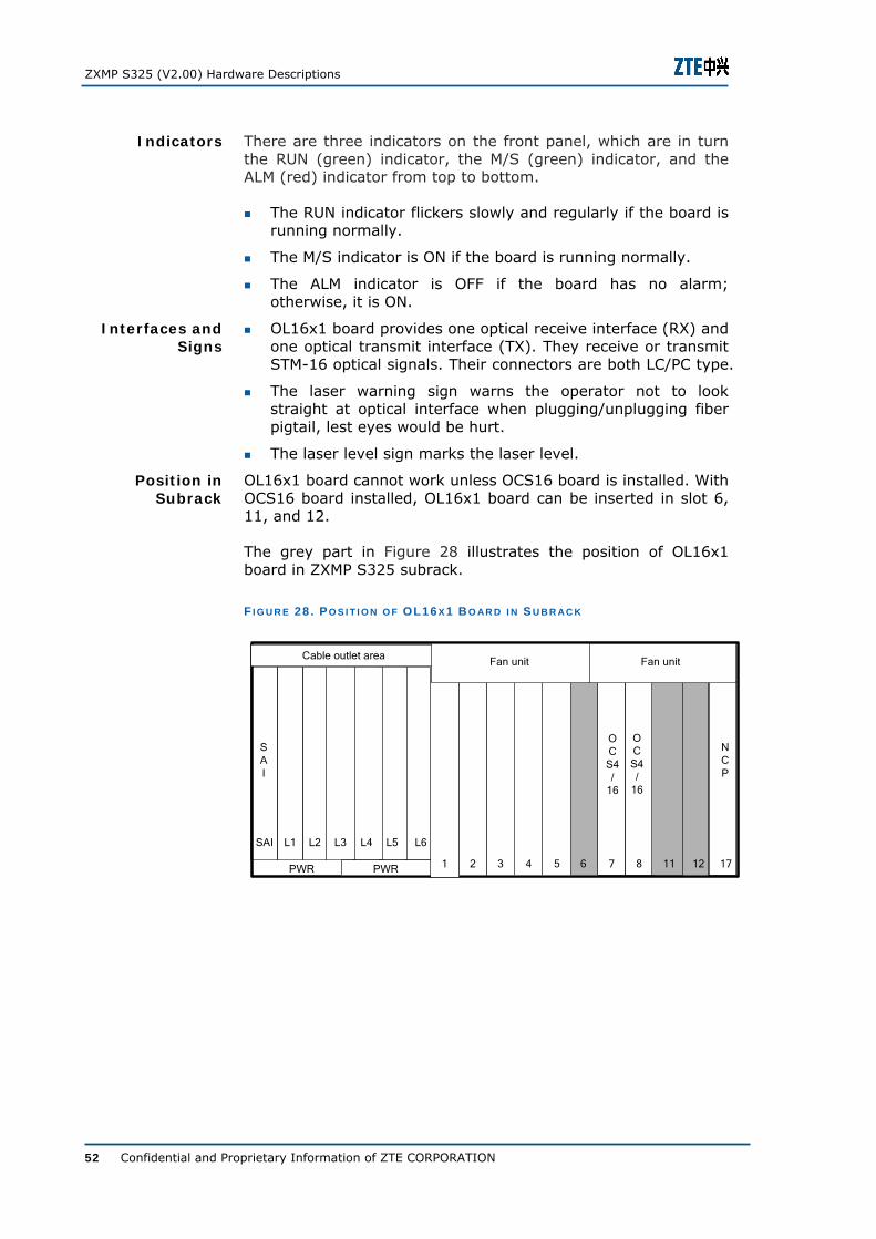
Citation preview
ZXMP S325SDH Based Multi-Service Node Equipment
Hardware Manual
Version 2.00
ZTE CORPORATION ZTE Plaza, Keji Road South, Hi-Tech Industrial Park, Nanshan District, Shenzhen, P. R. China 518057 Tel: (86) 755 26771900 800-9830-9830 Fax: (86) 755 26772236 URL: http://support.zte.com.cn E-mail: [email protected]
LEGAL INFORMATION Copyright © 2006 ZTE CORPORATION. The contents of this document are protected by copyright laws and international treaties. Any reproduction or distribution of this document or any portion of this document, in any form by any means, without the prior written consent of ZTE CORPORATION is prohibited. Additionally, the contents of this document are protected by contractual confidentiality obligations. All company, brand and product names are trade or service marks, or registered trade or service marks, of ZTE CORPORATION or of their respective owners. This document is provided “as is”, and all express, implied, or statutory warranties, representations or conditions are disclaimed, including without limitation any implied warranty of merchantability, fitness for a particular purpose, title or non-infringement. ZTE CORPORATION and its licensors shall not be liable for damages resulting from the use of or reliance on the information contained herein. ZTE CORPORATION or its licensors may have current or pending intellectual property rights or applications covering the subject matter of this document. Except as expressly provided in any written license between ZTE CORPORATION and its licensee, the user of this document shall not acquire any license to the subject matter herein. ZTE CORPORATION reserves the right to upgrade or make technical change to this product without further notice. Users may visit ZTE technical support website http://ensupport.zte.com.cn to inquire related information. The ultimate right to interpret this product resides in ZTE CORPORATION.
Revision History
Date Revision No. Serial No. Reason for Issue
2008/04/23 R1.0 sjzl20081227 First edition
ZTE CORPORATION Values Your Comments & Suggestions! Your opinion is of great value and will help us improve the quality of our product documentation and offer better services to our customers.
Please fax to: (86) 755-26772236; or mail to Documentation R&D Department, ZTE CORPORATION, ZTE Plaza, A Wing, Keji Road South, Hi-Tech Industrial Park, Shenzhen, P. R. China 518057.
Thank you for your cooperation!
Document Name ZXMP S325(V2.00) SDH Based Multi-Service Node Equipment Hardware Manual
Product Version V2.00 Document Revision Number R1.0
Serial No. sjzl20081227 Equipment Installation Date
Presentation: (Introductions, Procedures, Illustrations, Completeness, Level of Detail, Organization, Appearance)
Good Fair Average Poor Bad N/A
Accessibility: (Contents, Index, Headings, Numbering, Glossary)
Good Fair Average Poor Bad N/A
Your evaluation of this documentation
Intelligibility: (Language, Vocabulary, Readability & Clarity, Technical Accuracy, Content)
Good Fair Average Poor Bad N/A
Your suggestions for improvement of this documentation
Please check the suggestions which you feel can improve this documentation: Improve the overview/introduction Make it more concise/brief
Improve the Contents Add more step-by-step procedures/tutorials
Improve the organization Add more troubleshooting information
Include more figures Make it less technical
Add more examples Add more/better quick reference aids
Add more detail Improve the index
Other suggestions
__________________________________________________________________________
__________________________________________________________________________
__________________________________________________________________________
__________________________________________________________________________
__________________________________________________________________________
# Please feel free to write any comments on an attached sheet.
If you wish to be contacted regarding your comments, please complete the following:
Name Company
Postcode Address
Telephone E-mail

This page is intentionally blank.
Contents
About this Manual............................................................. i
Purpose................................................................................ i Intended Audience ................................................................. i Prerequisite Skill and Knowledge .............................................. i What is in This Manual............................................................ i Related Documentation.......................................................... ii Conventions......................................................................... ii How to Get in Touch............................................................. iii
Chapter 1.......................................................................... 5
Cabinet ............................................................................. 5
Cabinet Structure............................................................5
Basic Cabinet Fittings ......................................................7
Cabinet Configuration .................................................... 10
Chapter 2........................................................................11
Equipment Composition.................................................11
Structural Parts ............................................................ 11
Subrack....................................................................... 15
Fan Unit....................................................................... 17
Dustproof Unit .............................................................. 18
Power Distribution Box................................................... 19
Chapter 3........................................................................23
Boards ............................................................................23
Overview ..................................................................... 23 Subsystem Overview ........................................................... 23 Board Overview .................................................................. 24 Board Slots ........................................................................ 27
Board Structure ............................................................ 28
Functional/Service Interface Board ........................................ 28
Functional/Service Board......................................................29
Motherboard ................................................................ 30
NCP Unit...................................................................... 31 Overview ...........................................................................31 NCP Board..........................................................................31 SAI Board ..........................................................................36
Optical Line, Cross-connect, and Clock Unit....................... 39
Overview ...........................................................................39 OCS16 Board......................................................................39 OCS4 Board .......................................................................45
OL16x1 Board .............................................................. 50
OL1/4x4 Board ............................................................. 53
OL1/4 Subsystem ......................................................... 57 Overview ...........................................................................57 LP1x1/LP1x2/LP4x1/LP4x2 Boards .........................................59 OIS1x1/OIS1x2/OIS4x1/OIS4x2 Boards .................................61 ESS1x2 Board.....................................................................63 BIS1 Board.........................................................................64 Subsystem Configuration Example .........................................65
OA Board ..................................................................... 66
EP1 Subsystem............................................................. 70 Overview ...........................................................................70 EPE1x21/EPT1x21/EPE1B Boards...........................................71 ESE1x21 Board ...................................................................75 BIE1x21 Board....................................................................77 Subsystem Configuration Example .........................................78
EP3 Subsystem............................................................. 79 Overview ...........................................................................79 EP3x3 Board.......................................................................80 ESE3x3 Board.....................................................................82 BIE3x3 Board .....................................................................84 Subsystem Configuration Example .........................................84
EOS Subsystem ............................................................ 86 Overview ...........................................................................86 SFEx6 Board.......................................................................87 EIFEx4 Board......................................................................90 BIFE Board.........................................................................92 OIS1x4 Board .....................................................................93
Subsystem Configuration Example......................................... 94
ATM Subsystem ............................................................ 96
Overview ........................................................................... 96 AP1x4 Board ...................................................................... 97 Subsystem Configuration Example......................................... 99
RPR Subsystem .......................................................... 101 Overview ......................................................................... 101 RSEB Board ..................................................................... 102 Subsystem Configuration Example....................................... 105
PWR Board................................................................. 106
Appendix A...................................................................109
Terminologies ..............................................................109
Appendix B...................................................................113
Abbreviations...............................................................113
Figures..........................................................................117
Tables...........................................................................121

This page is intentionally blank.
Confidential and Proprietary Information of ZTE CORPORATION i
About this Manual
Purpose
This manual describes ZXMP S325 cabinet structure, equipment composition, and boards.
Intended Audience
This document is intended for engineers and technicians who perform system operation activities on ZXMP S325 SDH Based Multi-Service Node Equipment.
Prerequisite Skill and Knowledge
Users must have SDH basic technology to use this document effectively. Familiarity with the following is helpful:
ZXMP S325 system and its various components
Equipment structure
Boards
What is in This Manual
This manual contains the following chapters:
T AB L E 1 . C H AP T E R S U M M AR Y
Chapter Summary
Chapter 1 Cabinet Describes the structure, basic fittings, and configuration of the ZXMP S325 cabinet
Chapter 2 Equipment Composition
Describes the components of the ZXMP S325 equipment
Chapter 3 Boards Describes the boards of the ZXMP S325
ZXMP S325 (V2.00) Hardware Descriptions
ii Confidential and Proprietary Information of ZTE CORPORATION
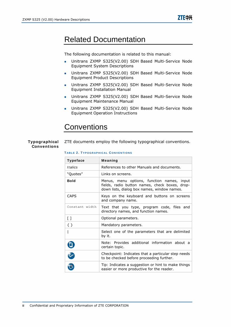
Related Documentation
The following documentation is related to this manual:
Unitrans ZXMP S325(V2.00) SDH Based Multi-Service Node Equipment System Descriptions
Unitrans ZXMP S325(V2.00) SDH Based Multi-Service Node Equipment Product Descriptions
Unitrans ZXMP S325(V2.00) SDH Based Multi-Service Node Equipment Installation Manual
Unitrans ZXMP S325(V2.00) SDH Based Multi-Service Node Equipment Maintenance Manual
Unitrans ZXMP S325(V2.00) SDH Based Multi-Service Node Equipment Operation Instructions
Conventions
ZTE documents employ the following typographical conventions.
T AB L E 2 . TY P O G R AP H I C AL C O N V E N T I O N S
Typeface Meaning
Italics References to other Manuals and documents.
“Quotes” Links on screens.
Bold Menus, menu options, function names, input fields, radio button names, check boxes, drop-down lists, dialog box names, window names.
CAPS Keys on the keyboard and buttons on screens and company name.
Constant width Text that you type, program code, files and directory names, and function names.
[ ] Optional parameters.
Mandatory parameters.
| Select one of the parameters that are delimited by it.
Note: Provides additional information about a certain topic.
Checkpoint: Indicates that a particular step needs to be checked before proceeding further.
Tip: Indicates a suggestion or hint to make things easier or more productive for the reader.
Typographical Conventions
About this Manual
Confidential and Proprietary Information of ZTE CORPORATION iii
T AB L E 3 . M O U S E OP E R AT I O N C O N V E N T I O N S
Typeface Meaning
Click Refers to clicking the primary mouse button (usually the left mouse button) once.
Double-click Refers to quickly clicking the primary mouse button (usually the left mouse button) twice.
Right-click Refers to clicking the secondary mouse button (usually the right mouse button) once.
Drag Refers to pressing and holding a mouse button and moving the mouse.
How to Get in Touch
The following sections provide information on how to obtain support for the documentation and the software.
If you have problems, questions, comments, or suggestions regarding your product, contact us by e-mail at [email protected]. You can also call our customer support center at (86) 755 26771900 and (86) 800-9830-9830.
ZTE welcomes your comments and suggestions on the quality and usefulness of this document. For further questions, comments, or suggestions on the documentation, you can contact us by e-mail at [email protected]; or you can fax your comments and suggestions to (86) 755 26772236. You can also browse our website at http://support.zte.com.cn, which contains various interesting subjects like documentation, knowledge base, forum and service request.
Mouse Operation Conventions
Customer Support
Documentation Support

ZXMP S325 (V2.00) Hardware Descriptions
iv Confidential and Proprietary Information of ZTE CORPORATION
This page is intentionally blank.
Confidential and Proprietary Information of ZTE CORPORATION 5
C h a p t e r 1
Cabinet
Cabinet Structure ZXMP S325 cabinet employs the “IEC 19-inch cabinet +
subrack” structure. The cabinet and subracks satisfy the requirements of operation and maintenance from the front.
ZXMP S325 cabinet comprises metal materials, featuring excellent electromagnetic shielding performance and heat dissipation performance.
The three cabinet heights for ZXMP S325 are: 2000 mm, 2200 mm, and 2600 mm.
Table 4 lists the cabinet dimensions and weights.
T AB L E 4 . C AB I N E T D I M E N S I O N S AN D W E I G H T S
Dimensions (Height × Width × Depth)(Unit: mm) Weight (Unit: kg)
2000 × 600 × 300 70
2000 × 600 × 300 80
2600 × 600 × 300 90
Notes:
The weights are those of empty cabinets.
ZTE can provide the cabinet 600 mm deep as per user requirement.
The cabinet front door, rear door, and side panels are always detached in the figures shown in this manual in order to show the equipment inner structure clearly.
In practice, the front door is opened from the left, and the side panels cannot be detached.
Description
ZXMP S325 (V2.00) Hardware Descriptions
6 Confidential and Proprietary Information of ZTE CORPORATION
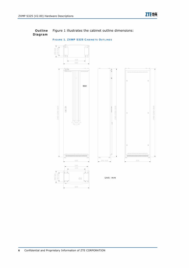
Figure 1 illustrates the cabinet outline dimensions:
F I G U R E 1 . ZXMP S325 C AB I N E T S OU T L I N E S
Unit: mm
Outline Diagram

Chapter 1 - Cabinet
Confidential and Proprietary Information of ZTE CORPORATION 7
Basic Cabinet Fittings Figure 2 illustrates the basic fittings of a 2200 mm high cabinet. Table 5 briefly describes these fittings.
F I G U R E 2 . B AS I C F I T T I N G S O F A 2200 M M H I G H ZXMP S325 C AB I N E T
1. Cable securing plate 2. Cable wiring clip 3. Cabinet cabling area 4. Ring trip switch 5. Ring trip reset button 6. Grounding copper busbar 7. Mounting bracket 8. Small cabling door 9. Power cable outlet 10. Top outlet 11. Alarm indicator board 12. Hook for antistatic wrist strap 13. Socket for antistatic wrist strap 14. Door lock 15. Front door 16. Bottom outlet
Overview
ZXMP S325 (V2.00) Hardware Descriptions
8 Confidential and Proprietary Information of ZTE CORPORATION
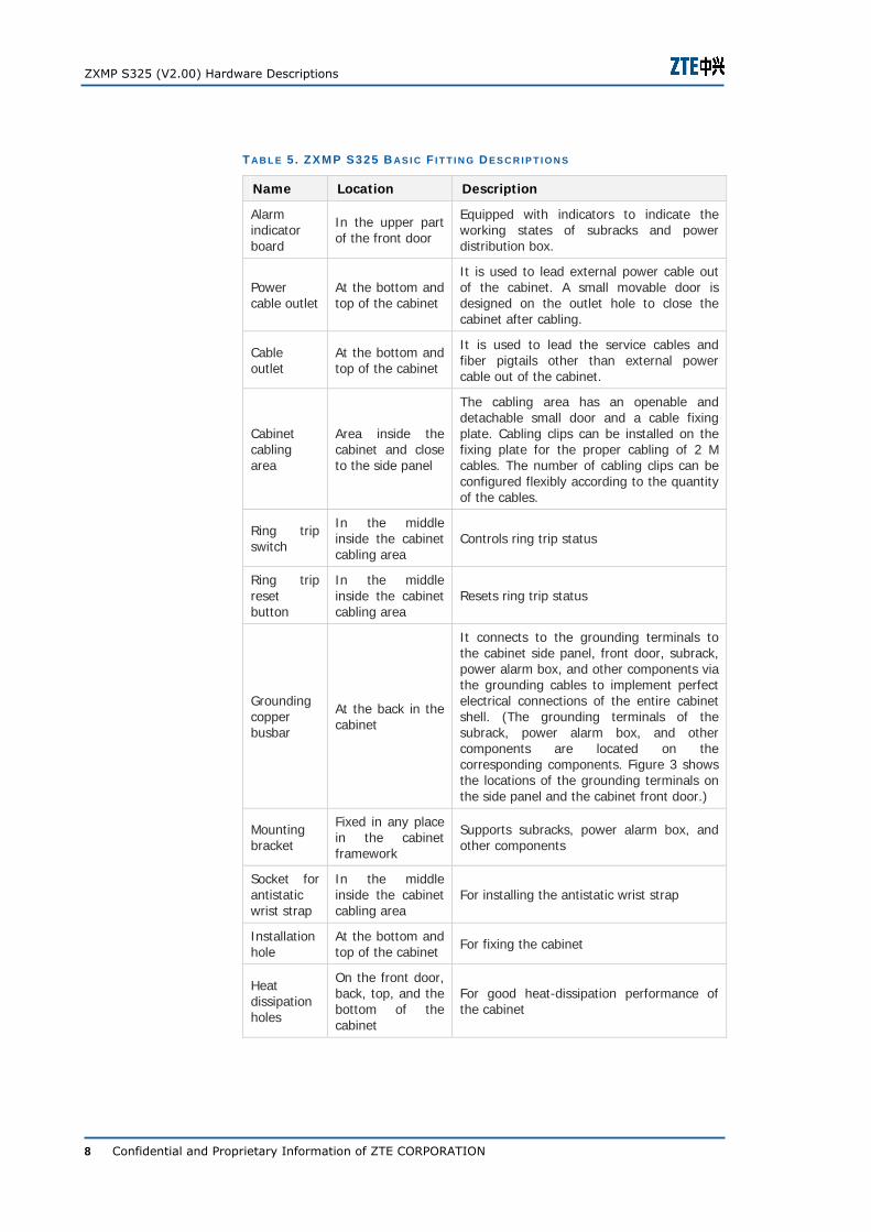
T AB L E 5 . ZXMP S325 B AS I C F I T T I N G D E S C R I P T I O N S
Name Location Description
Alarm indicator board
In the upper part of the front door
Equipped with indicators to indicate the working states of subracks and power distribution box.
Power cable outlet
At the bottom and top of the cabinet
It is used to lead external power cable out of the cabinet. A small movable door is designed on the outlet hole to close the cabinet after cabling.
Cable outlet
At the bottom and top of the cabinet
It is used to lead the service cables and fiber pigtails other than external power cable out of the cabinet.
Cabinet cabling area
Area inside the cabinet and close to the side panel
The cabling area has an openable and detachable small door and a cable fixing plate. Cabling clips can be installed on the fixing plate for the proper cabling of 2 M cables. The number of cabling clips can be configured flexibly according to the quantity of the cables.
Ring trip switch
In the middle inside the cabinet cabling area
Controls ring trip status
Ring trip reset button
In the middle inside the cabinet cabling area
Resets ring trip status
Grounding copper busbar
At the back in the cabinet
It connects to the grounding terminals to the cabinet side panel, front door, subrack, power alarm box, and other components via the grounding cables to implement perfect electrical connections of the entire cabinet shell. (The grounding terminals of the subrack, power alarm box, and other components are located on the corresponding components. Figure 3 shows the locations of the grounding terminals on the side panel and the cabinet front door.)
Mounting bracket
Fixed in any place in the cabinet framework
Supports subracks, power alarm box, and other components
Socket for antistatic wrist strap
In the middle inside the cabinet cabling area
For installing the antistatic wrist strap
Installation hole
At the bottom and top of the cabinet For fixing the cabinet
Heat dissipation holes
On the front door, back, top, and the bottom of the cabinet
For good heat-dissipation performance of the cabinet
Chapter 1 - Cabinet
Confidential and Proprietary Information of ZTE CORPORATION 9
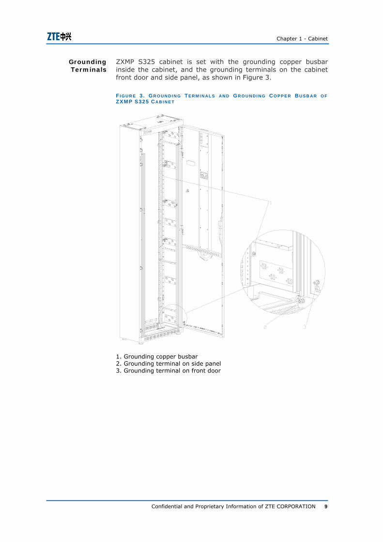
ZXMP S325 cabinet is set with the grounding copper busbar inside the cabinet, and the grounding terminals on the cabinet front door and side panel, as shown in Figure 3.
F I G U R E 3 . GR O U N D I N G TE R M I N AL S AN D GR O U N D I N G C O P P E R B U S B AR O F ZXMP S325 CAB I N E T
1. Grounding copper busbar 2. Grounding terminal on side panel 3. Grounding terminal on front door
Grounding Terminals
ZXMP S325 (V2.00) Hardware Descriptions
10 Confidential and Proprietary Information of ZTE CORPORATION
Cabinet Configuration The different cabinet configurations are similar. ZXMP S325
equipment with basic configuration comprises cabinet, subracks, power distribution box, and dustproof unit.
Table 6 lists the configuration of the ZXMP S325 in a single cabinet.
T AB L E 6 . C O N F I G U R AT I O N O F ZXMP S325 I N A S I N G L E C AB I N E T
Cabinet Height (Unit: mm)
Effective Height
Number of Power Distribution Box (Height: 3U)
Number of Subrack (Height: 5U)
2000 42U 1 4
2200 47U 1 4
2600 56U 1 4
Notes: 1. 1 U = 44.45 mm 2. The capacity of 2 Mbps service and cablings in full configuration has been
taken into account. 3. The power distribution box is the unified one of ZTE transmission equipment
with the height of 3U. 4. The subracks are arranged top down in the order of subrack 1, subrack 2,
subrack 3, and subrack 4.
The ZXMP S325 equipment can cooperate with other ZTE SDH equipment flexibly, such as ZXMP S320, ZXMP S330, ZXMP S360, ZXMP S390, ZXMP S380, and ZXMP S385.
Configuration Description
Cooperation with Other
ZTE SDH Equipment
Confidential and Proprietary Information of ZTE CORPORATION 11
C h a p t e r 2
Equipment Composition
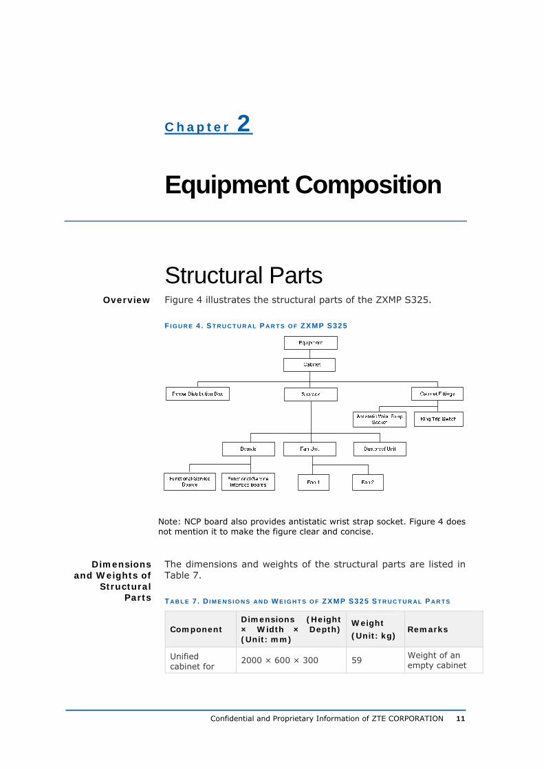
Structural Parts Figure 4 illustrates the structural parts of the ZXMP S325.
F I G U R E 4 . S T R U C T U R AL P A R T S O F ZXMP S325
Note: NCP board also provides antistatic wrist strap socket. Figure 4 does not mention it to make the figure clear and concise.
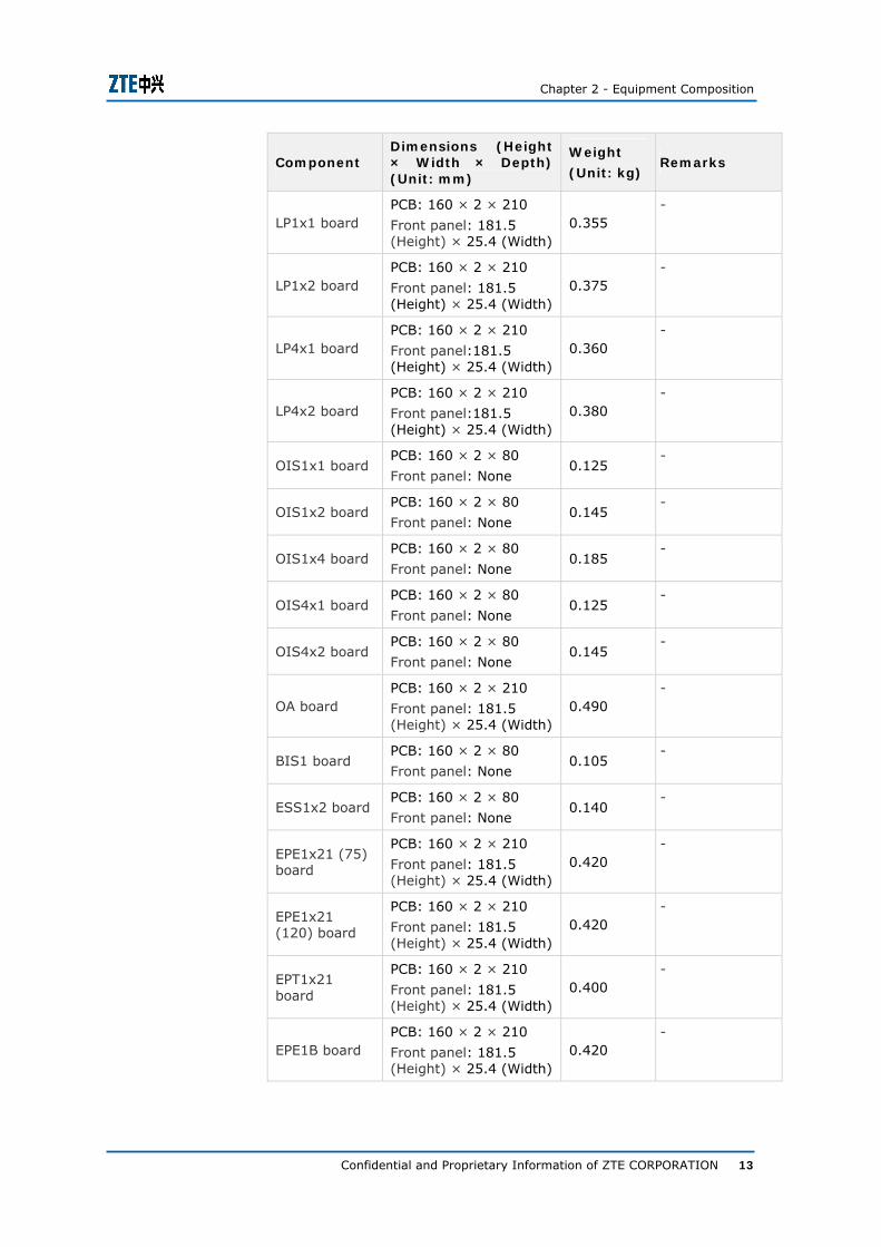
The dimensions and weights of the structural parts are listed in Table 7.
T AB L E 7 . D I M E N S I O N S AN D W E I G H T S O F ZXMP S325 S T R U C T U R AL P A R T S
Component Dimensions (Height × Width × Depth) (Unit: mm)
Weight
(Unit: kg) Remarks
Unified cabinet for
2000 × 600 × 300 59 Weight of an empty cabinet
Overview
Dimensions and Weights of
Structural Parts
ZXMP S325 (V2.00) Hardware Descriptions
12 Confidential and Proprietary Information of ZTE CORPORATION
Component Dimensions (Height × Width × Depth) (Unit: mm)
Weight
(Unit: kg) Remarks
2200× 600 × 300 65 Weight of an empty cabinet
ZTE transmission equipment
2600 × 600 × 300 77 Weight of an empty cabinet
ZXMP S325 subrack
221.45 × 482.6 × 270 9 Weight of an empty subrack
Motherboard (MB)
214.6 × 438.4 × 4.5 1.500 -
3U power distribution box (PDB)
132.5 × 482.6 × 269.5 7 Includes electronic components
Dustproof unit 13.1 × 279.6 × 253 - Its weight is included in subrack.
Fan box PCB: 90 × 79 × 1.6
21.5 × 139.6 × 244.8 0.520
Includes structural parts and circuits
NCP board PCB: 160 × 2× 210
Front panel: 181.5 (Height) × 25.4 (Width)
0.430 -
SAI board PCB: 160 × 2 × 80
Front panel: None 0.160
-
PWRA board PCB: 2 × 72 × 170
Front panel: 25 (Height) × 74 (Width)
0.160 -
OCS16 board PCB: 160 × 2 × 210
Front panel: 181.5 (Height) × 25.4 (Width)
0.460 -
OCS4 board PCB: 160 × 2 × 210
Front panel: 181.5 (Height) × 25.4 (Width)
0.550 -
OL16x1 board PCB: 160 × 2 × 210
Front panel: 181.5 (Height) × 25.4 (Width)
0.410 -
0.425 OL1/4x4(1x STM-1/4)
0.445 OL1/4x4(2x STM-1/4)
0.465 OL1/4x4(3x STM-1/4)
OL1/4x4 board
PCB: 160 × 2 × 210
Front panel: 181.5 (Height) × 25.4 (Width)
0.485 OL1/4x4(4x STM-1/4)
Chapter 2 - Equipment Composition
Confidential and Proprietary Information of ZTE CORPORATION 13
Component Dimensions (Height × Width × Depth) (Unit: mm)
Weight
(Unit: kg) Remarks
LP1x1 board PCB: 160 × 2 × 210
Front panel: 181.5 (Height) × 25.4 (Width)
0.355 -
LP1x2 board PCB: 160 × 2 × 210
Front panel: 181.5 (Height) × 25.4 (Width)
0.375 -
LP4x1 board PCB: 160 × 2 × 210
Front panel:181.5 (Height) × 25.4 (Width)
0.360 -
LP4x2 board PCB: 160 × 2 × 210
Front panel:181.5 (Height) × 25.4 (Width)
0.380 -
OIS1x1 board PCB: 160 × 2 × 80
Front panel: None 0.125
-
OIS1x2 board PCB: 160 × 2 × 80
Front panel: None 0.145
-
OIS1x4 board PCB: 160 × 2 × 80
Front panel: None 0.185
-
OIS4x1 board PCB: 160 × 2 × 80
Front panel: None 0.125
-
OIS4x2 board PCB: 160 × 2 × 80
Front panel: None 0.145
-
OA board PCB: 160 × 2 × 210
Front panel: 181.5 (Height) × 25.4 (Width)
0.490 -
BIS1 board PCB: 160 × 2 × 80
Front panel: None 0.105
-
ESS1x2 board PCB: 160 × 2 × 80
Front panel: None 0.140
-
EPE1x21 (75) board
PCB: 160 × 2 × 210
Front panel: 181.5 (Height) × 25.4 (Width)
0.420 -
EPE1x21 (120) board
PCB: 160 × 2 × 210
Front panel: 181.5 (Height) × 25.4 (Width)
0.420 -
EPT1x21 board
PCB: 160 × 2 × 210
Front panel: 181.5 (Height) × 25.4 (Width)
0.400 -
EPE1B board PCB: 160 × 2 × 210
Front panel: 181.5 (Height) × 25.4 (Width)
0.420 -
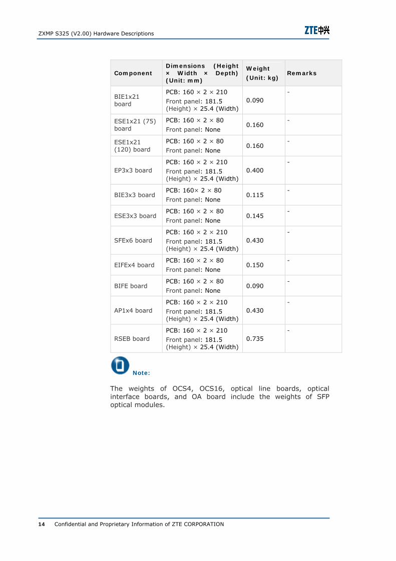
ZXMP S325 (V2.00) Hardware Descriptions
14 Confidential and Proprietary Information of ZTE CORPORATION
Component Dimensions (Height × Width × Depth) (Unit: mm)
Weight
(Unit: kg) Remarks
BIE1x21 board
PCB: 160 × 2 × 210
Front panel: 181.5 (Height) × 25.4 (Width)
0.090 -
ESE1x21 (75) board
PCB: 160 × 2 × 80
Front panel: None 0.160
-
ESE1x21 (120) board
PCB: 160 × 2 × 80
Front panel: None 0.160
-
EP3x3 board PCB: 160 × 2 × 210
Front panel: 181.5 (Height) × 25.4 (Width)
0.400 -
BIE3x3 board PCB: 160× 2 × 80
Front panel: None 0.115
-
ESE3x3 board PCB: 160 × 2 × 80
Front panel: None 0.145
-
SFEx6 board PCB: 160 × 2 × 210
Front panel: 181.5 (Height) × 25.4 (Width)
0.430 -
EIFEx4 board PCB: 160 × 2 × 80
Front panel: None 0.150
-
BIFE board PCB: 160 × 2 × 80
Front panel: None 0.090
-
AP1x4 board PCB: 160 × 2 × 210
Front panel: 181.5 (Height) × 25.4 (Width)
0.430 -
RSEB board PCB: 160 × 2 × 210
Front panel: 181.5 (Height) × 25.4 (Width)
0.735 -
Note:
The weights of OCS4, OCS16, optical line boards, optical interface boards, and OA board include the weights of SFP optical modules.
Chapter 2 - Equipment Composition
Confidential and Proprietary Information of ZTE CORPORATION 15
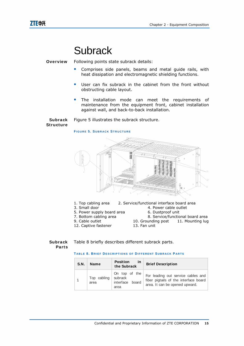
Subrack Following points state subrack details:
Comprises side panels, beams and metal guide rails, with heat dissipation and electromagnetic shielding functions.
User can fix subrack in the cabinet from the front without obstructing cable layout.
The installation mode can meet the requirements of maintenance from the equipment front, cabinet installation against wall, and back-to-back installation.
Figure 5 illustrates the subrack structure.
F I G U R E 5 . S U B R AC K S T R U C T U R E
1. Top cabling area 2. Service/functional interface board area 3. Small door 4. Power cable outlet 5. Power supply board area 6. Dustproof unit 7. Bottom cabling area 8. Service/functional board area 9. Cable outlet 10. Grounding post 11. Mounting lug 12. Captive fastener 13. Fan unit
Table 8 briefly describes different subrack parts.
T AB L E 8 . B R I E F D E S C R I P T I O N S O F D I F F E R E N T S U B R AC K P AR T S
S.N. Name Position in the Subrack Brief Description
1 Top cabling area
On top of the subrack interface board area
For leading out service cables and fiber pigtails of the interface board area. It can be opened upward.
Overview
Subrack Structure
Subrack Parts
ZXMP S325 (V2.00) Hardware Descriptions
16 Confidential and Proprietary Information of ZTE CORPORATION
S.N. Name Position in the Subrack Brief Description
2
Service/functional interface board area
In the upper left part of the subrack
The system interface board (SAI) and the service interface boards are inserted in this area. This area has one slot for the system interface board, and six slots for service interface boards. The board slots are arranged as in Figure 10.
3 Small door On the left side of the subrack
For the purposes of decoration, ventilation, and shielding. It is detachable.
4 Power cable outlet
At the bottom of the subrack left panel.
For leading out the power cable.
5 Power supply board area
In the bottom left part of the subrack
To insert the power supply board
6 Dustproof unit
At the bottom of the service/ functional board area
Keep the subrack inside clean, thus ensuring heat dissipation performance
7 Bottom cabling area
At the bottom of the subrack and above the dustproof unit
For laying service cables and fiber pigtails of the service/functional board area
8 Service/Functional board area
At the right side of the subrack
To insert the functional/service boards. It has 11 slots, with a 25.4 mm gap between neighboring slots. The board slots are arranged as in Figure 10.
9 Cable outletAt the bottom of the subrack right panel
For leading out service cables and fiber pigtails of the service/functional board area.
10 Grounding post
At the bottom of the subrack right panel
For connecting the subrack protection ground cable.
11 Mounting lug
At the back of the subrack (one each on the left and the right)
For fixing a subrack in the cabinet
12 Captive fastener
On the mounting lug For fixing a subrack in the cabinet
13 Fan unit On top of the subrack right side
It provides forced air cooling for the equipment to dissipate heat. The fan unit has two independent fan boxes, each of which is connected to the fan motherboard (FMB) for the convenience of maintenance.
Chapter 2 - Equipment Composition
Confidential and Proprietary Information of ZTE CORPORATION 17
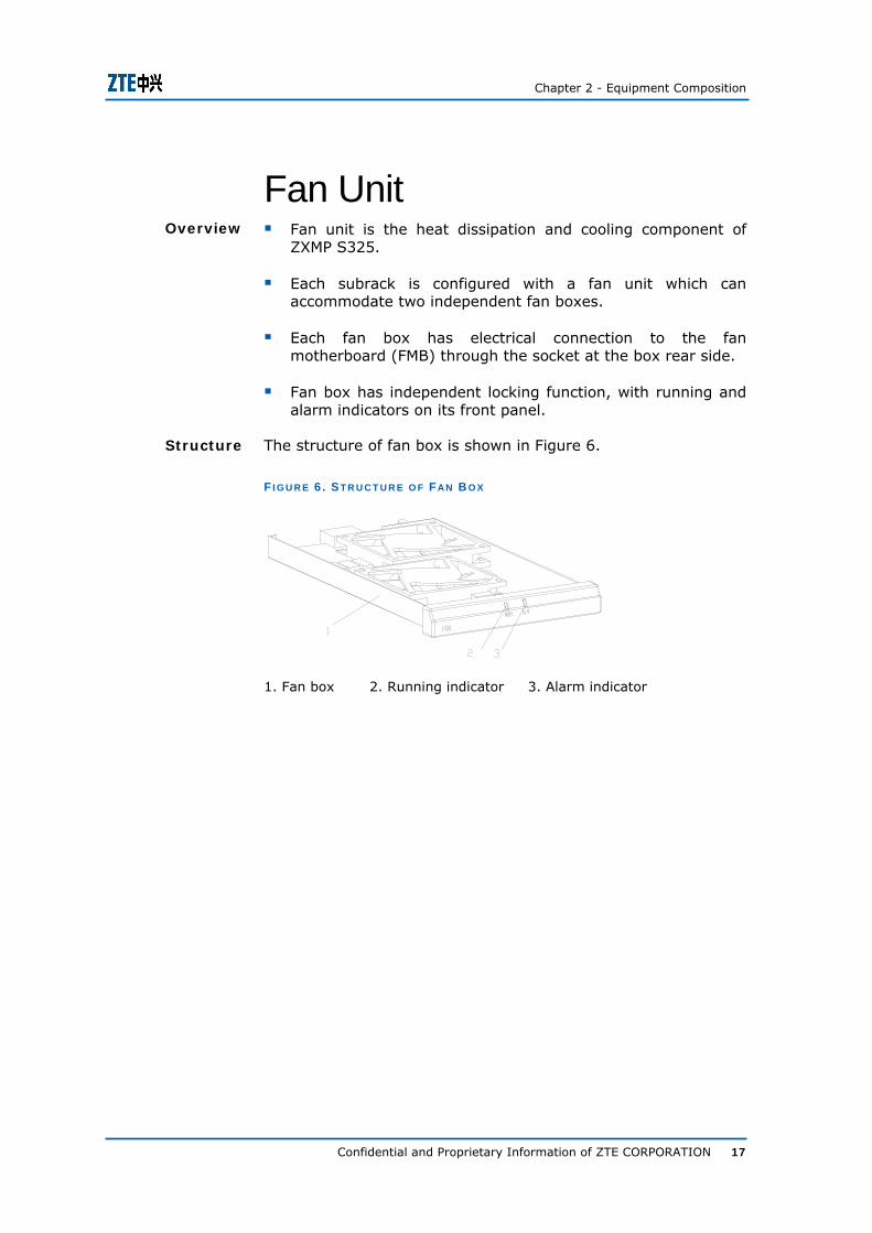
Fan Unit Fan unit is the heat dissipation and cooling component of
ZXMP S325.
Each subrack is configured with a fan unit which can accommodate two independent fan boxes.
Each fan box has electrical connection to the fan motherboard (FMB) through the socket at the box rear side.
Fan box has independent locking function, with running and alarm indicators on its front panel.
The structure of fan box is shown in Figure 6.
F I G U R E 6 . S T R U C T U R E O F FAN B O X
1. Fan box 2. Running indicator 3. Alarm indicator
Overview
Structure
ZXMP S325 (V2.00) Hardware Descriptions
18 Confidential and Proprietary Information of ZTE CORPORATION
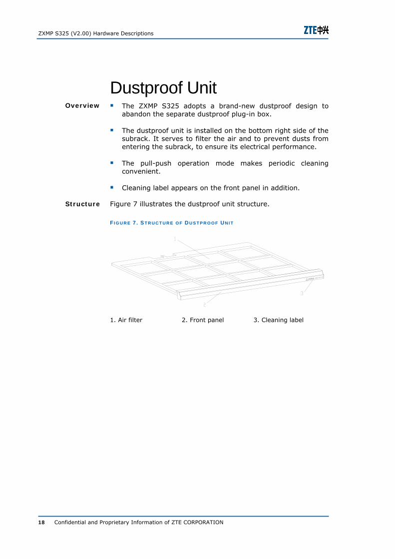
Dustproof Unit The ZXMP S325 adopts a brand-new dustproof design to
abandon the separate dustproof plug-in box.
The dustproof unit is installed on the bottom right side of the subrack. It serves to filter the air and to prevent dusts from entering the subrack, to ensure its electrical performance.
The pull-push operation mode makes periodic cleaning convenient.
Cleaning label appears on the front panel in addition.
Figure 7 illustrates the dustproof unit structure.
F I G U R E 7 . S T R U C T U R E O F D U S T P R O O F UN I T
1. Air filter 2. Front panel 3. Cleaning label
Overview
Structure
Chapter 2 - Equipment Composition
Confidential and Proprietary Information of ZTE CORPORATION 19
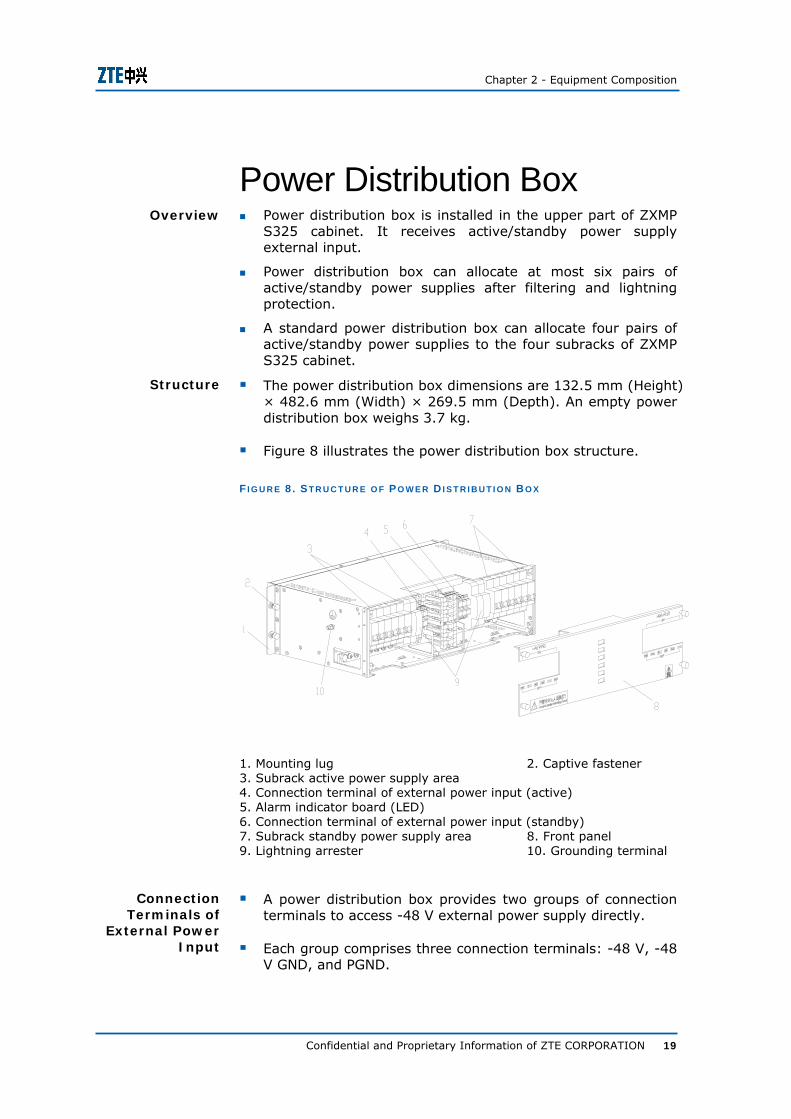
Power Distribution Box Power distribution box is installed in the upper part of ZXMP
S325 cabinet. It receives active/standby power supply external input.
Power distribution box can allocate at most six pairs of active/standby power supplies after filtering and lightning protection.
A standard power distribution box can allocate four pairs of active/standby power supplies to the four subracks of ZXMP S325 cabinet.
The power distribution box dimensions are 132.5 mm (Height) × 482.6 mm (Width) × 269.5 mm (Depth). An empty power distribution box weighs 3.7 kg.
Figure 8 illustrates the power distribution box structure.
F I G U R E 8 . S T R U C T U R E O F P O W E R D I S T R I B U T I O N B O X
1. Mounting lug 2. Captive fastener 3. Subrack active power supply area 4. Connection terminal of external power input (active) 5. Alarm indicator board (LED) 6. Connection terminal of external power input (standby) 7. Subrack standby power supply area 8. Front panel 9. Lightning arrester 10. Grounding terminal
A power distribution box provides two groups of connection terminals to access -48 V external power supply directly.
Each group comprises three connection terminals: -48 V, -48 V GND, and PGND.
Overview
Structure
Connection Terminals of
External Power Input
ZXMP S325 (V2.00) Hardware Descriptions
20 Confidential and Proprietary Information of ZTE CORPORATION
The left group is for the active power input and the right group is for the standby power input by default.
A power distribution box can provide at most six pairs of active/standby power supplies.
With standard configuration, a power distribution box provides four pairs of active/standby power supplies.
Each power supply includes a -48 V, a -48 V GND, and a PGND power supply, which are controlled by an air switch.
Each pair of active/standby power supply provides 1+1 power supply protection for a subrack in a cabinet.
The alarm indicator board (LED) displays the equipment cabinet alarms, which is synchronous with alarm indicators on the alarm indicator board of the equipment cabinet.
There are green, yellow, and red indicators, which respectively indicate normal power supply, minor alarms, and critical/major alarms of the equipment.
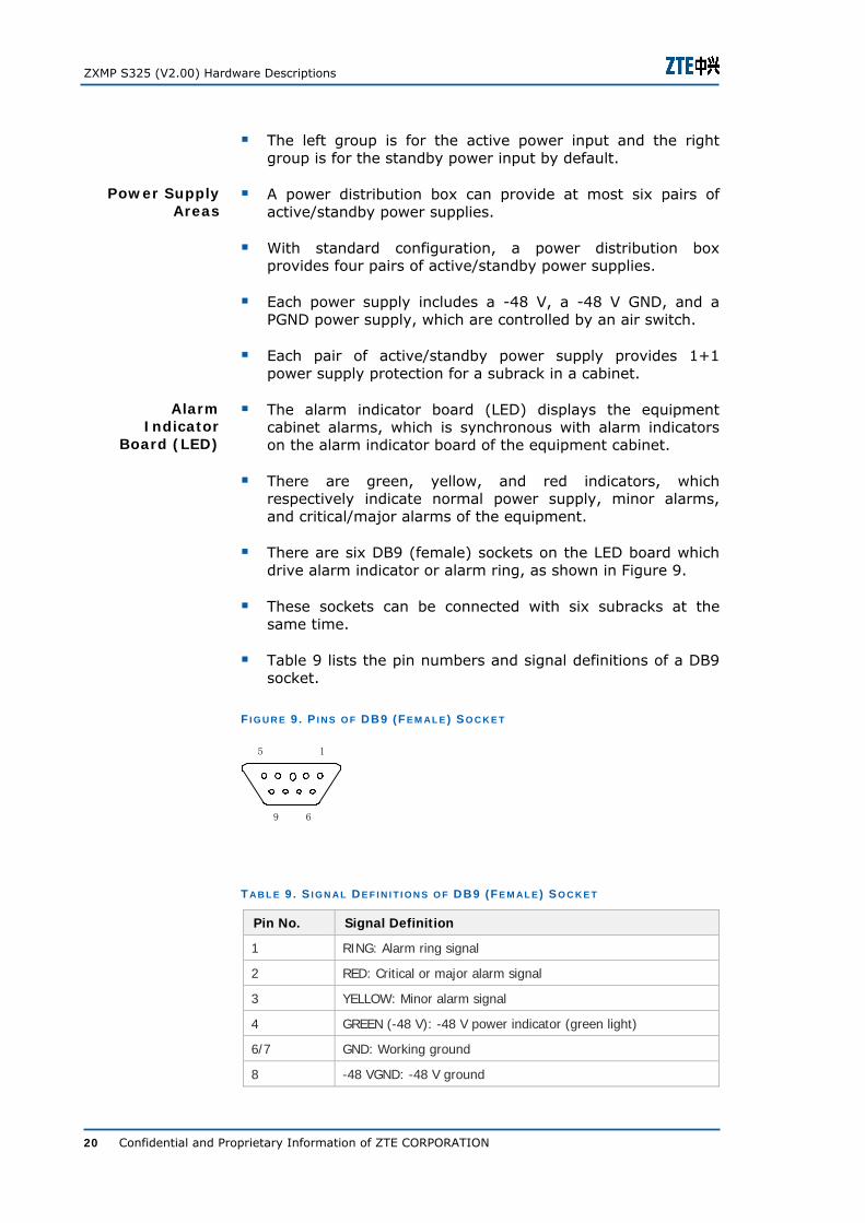
There are six DB9 (female) sockets on the LED board which drive alarm indicator or alarm ring, as shown in Figure 9.
These sockets can be connected with six subracks at the same time.
Table 9 lists the pin numbers and signal definitions of a DB9 socket.
F I G U R E 9 . P I N S O F DB9 (FE M AL E ) S O C K E T
15
9 6
T AB L E 9 . S I G N AL D E F I N I T I O N S O F DB9 (FE M AL E ) S O C K E T
Pin No. Signal Definition
1 RING: Alarm ring signal
2 RED: Critical or major alarm signal
3 YELLOW: Minor alarm signal
4 GREEN (-48 V): -48 V power indicator (green light)
6/7 GND: Working ground
8 -48 VGND: -48 V ground
Power Supply Areas
Alarm Indicator
Board (LED)
Chapter 2 - Equipment Composition
Confidential and Proprietary Information of ZTE CORPORATION 21
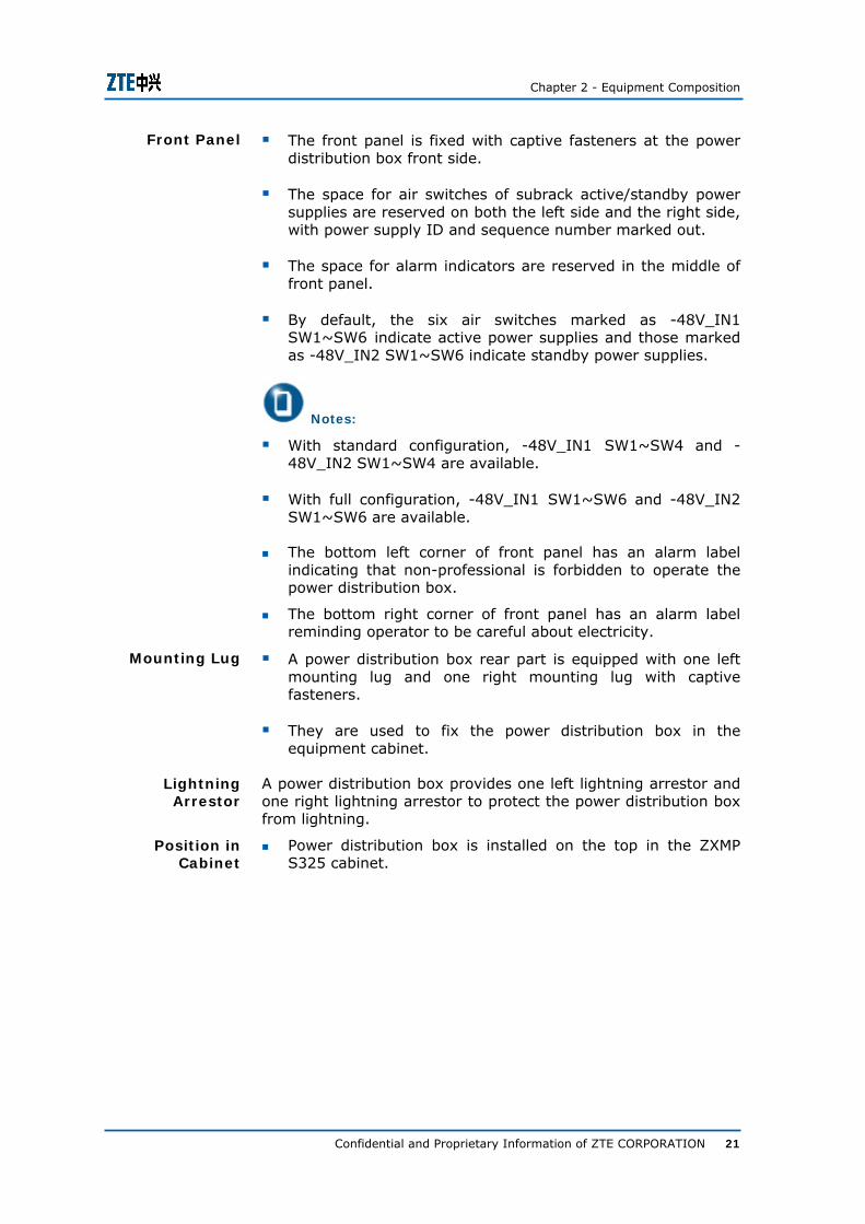
The front panel is fixed with captive fasteners at the power distribution box front side.
The space for air switches of subrack active/standby power supplies are reserved on both the left side and the right side, with power supply ID and sequence number marked out.
The space for alarm indicators are reserved in the middle of front panel.
By default, the six air switches marked as -48V_IN1 SW1~SW6 indicate active power supplies and those marked as -48V_IN2 SW1~SW6 indicate standby power supplies.
Notes:
With standard configuration, -48V_IN1 SW1~SW4 and -48V_IN2 SW1~SW4 are available.
With full configuration, -48V_IN1 SW1~SW6 and -48V_IN2 SW1~SW6 are available.
The bottom left corner of front panel has an alarm label indicating that non-professional is forbidden to operate the power distribution box.
The bottom right corner of front panel has an alarm label reminding operator to be careful about electricity.
A power distribution box rear part is equipped with one left mounting lug and one right mounting lug with captive fasteners.
They are used to fix the power distribution box in the equipment cabinet.
A power distribution box provides one left lightning arrestor and one right lightning arrestor to protect the power distribution box from lightning.
Power distribution box is installed on the top in the ZXMP S325 cabinet.
Front Panel
Mounting Lug
Lightning Arrestor
Position in Cabinet

ZXMP S325 (V2.00) Hardware Descriptions
22 Confidential and Proprietary Information of ZTE CORPORATION
This page is intentionally blank.
Confidential and Proprietary Information of ZTE CORPORATION 23
C h a p t e r 3
Boards
Overview This chapter describes boards based on units and subsystems, since the boards of ZXMP S325 are designed according to units and subsystems. Each unit or subsystem performs a certain function.
The positions and connection relations of all the boards in a unit or subsystem are described in the unit/subsystem overview.
The functions, functional blocks, front panel, interfaces, and indicators of a board are described in the section of this board.
Subsystem Overview
The boards of ZXMP S325 are designed based on units and subsystems. Each unit or subsystem performs a certain function. Table 10 illustrates the units and subsystems of ZXMP S325.
T AB L E 10 . U N I T S AN D S U B S Y S T E M S O F ZXMP S325
Subsystem/Unit ID
Full Name Boards Involved
NCPU NE control processor unit
NCP, SAI
- Optical line, cross-connect, and clock unit
OCS4, OCS16, SAI
EP1 E1/T1 electrical tributary subsystem
EPE1x21, EPT1x21, EPE1B, ESE1x21, BIE1x21
EP3 E3/T3 electrical tributary subsystem
EP3x3, ESE3x3, BIE3x3
ZXMP S325 (V2.00) Hardware Descriptions
24 Confidential and Proprietary Information of ZTE CORPORATION
Subsystem/Unit ID
Full Name Boards Involved
OL1/4 STM-1/STM-4 optical line subsystem
LP1x1, LP1x2, LP4x1, LP4x2, OIS1x1, OIS1x2, OIS4x1, OIS4x2, ESS1x2, BIS1
EOS EOS subsystem SFEx6, EIFEx4, OIS1x4, BIFE
ATM ATM subsystem AP1x4, OIS1x4
RPR RPR subsystem RSEB, OIS1x4, EIFEx4
Board Overview
Table 11 lists all the ZXMP S325 boards.
T AB L E 11 . ZXMP S325 B O AR D S
Board ID Board/Unit Name Remarks
MB Motherboard -
SAI System auxiliary interface board
-
NCP NE control processor Has orderwire function. Applicable to ZXMP S330.
PWR Power supply board -
OCS4
STM-1/4 optical line, cross-connect, and synchronous-clock board
-
OCS16
STM-16 optical line, cross-connect, and synchronous-clock board
-
LP1x1 1-channel STM-1 line processor
LP1x2 2-channel STM-1 line processor
LP4x1 1-channel STM-4 line processor
LP4x2 2-channel STM-4 line processor
Applicable to ZXMP S330.
OL1/4x4 4-channel STM-1/STM-4 optical line board
With different optical modules, it can work as STM-1 or STM-4 optical line board.
Applicable to ZXMP S330.
Chapter 3 - Boards
Confidential and Proprietary Information of ZTE CORPORATION 25
Board ID Board/Unit Name Remarks
OL16x1 1-channel STM-16 optical line board
Applicable to ZXMP S330.
OIS1x1 1-channel STM-1 optical interface board
OIS1x2 2-channel STM-1 optical interface board
OIS1x4 4-channel STM-1 optical interface board
OIS4x1 1-channel STM-4 optical interface board
OIS4x2 2-channel STM-4 optical interface board
Applicable to ZXMP S330.
BIS1 STM-1 bridge interface board
Serves for STM-1 electrical interface protection. Applicable to ZXMP S330.
ESS1x2 2-channel STM-1 electrical interface switching board
Applicable to ZXMP S330.
EPE1x21 (75)
21-channel E1 electrical processor (75 Ω)
The interface impedance is 75 Ω.
Applicable to ZXMP S330.
EPE1x21 (120)
21-channel E1 electrical processor (120 Ω)
The interface impedance is 120 Ω.
Applicable to ZXMP S330.
EPT1x21 (100)
21-channel T1 electrical processor (100 Ω)
The interface impedance is 100 Ω.
Applicable to ZXMP S330.
EPE1B 21-channel E1/T1 electrical processor
Supports the framing mode. Applicable to ZXMP S330.
BIE1x21 21-channel E1/T1 bridge interface board
Serves for E1/T1 board protection. Inserted in the interface board slot corresponding to the E1/T1 protection board.
Applicable to ZXMP S330.
ESE1x21 (75)
21-channel E1 electrical interface switching board (75 Ω)
The interface impedance is 75 Ω. Applicable to ZXMP S330.
ESE1x21 (120)
21-channel E1/T1 electrical interface switching board (120 Ω/100 Ω)
The interface impedance is 120 Ω or 100 Ω. Applicable to ZXMP S330.
EP3x3 3-channel E3/T3 electrical processor
Applicable to ZXMP S330.
ZXMP S325 (V2.00) Hardware Descriptions
26 Confidential and Proprietary Information of ZTE CORPORATION
Board ID Board/Unit Name Remarks
BIE3x3 3-channel E3/T3 electrical bridge interface board
Serves for E3/T3 board protection. Inserted in the interface board slot corresponding to the E3/T3 protection board.
Applicable to ZXMP S330.
ESE3x3 3-channel E3/T3 electrical interface switching board
Applicable to ZXMP S330.
SFEx6 Smart fast Ethernet board
There are two types of SFEx6 boards corresponding to different encapsulation modes: SFEx6 (PPP) board and SFEx6 (GFP) board.
Applicable to ZXMP S330.
EIFEx4 4-channel electrical interface board of fast Ethernet
Applicable to ZXMP S330.
BIFE Bridge interface board of fast Ethernet
Serves for SFEx6 board protection. Inserted in the interface board slot corresponding to the SFEx6 protection board.
Applicable to ZXMP S330.
AP1x4 ATM processor with 4 STM-1 ports
Applicable to ZXMP S330.
RSEB Ethernet processor with RPR function
Applicable to ZXMP S330.
OA Optical amplifier Applicable to ZXMP S330.
These boards fall into two categories:
Functional/service processor boards, including:
MB, OCS4, SAI, NCP, PWR, LP1x1, LP1x2, LP4x1, LP4x2, EPE1x21 (75), EPE1x21 (120), EPE1x21 (100), EPE1B, BIE1x21, ESE1x21 (75), ESE1x21 (120), EPE3x3, EPT3x3, EP3x3, SFEx6, AP1x4, OA, RSEB
Functional/service interface boards, including:
OIS1x1, OIS1x2, OIS1x4, OIS4x1, OIS4x2, BIS1, ESS1x2, BIE3x3, ESE3x3, EIFEx4, BIFE
Categories
Chapter 3 - Boards
Confidential and Proprietary Information of ZTE CORPORATION 27
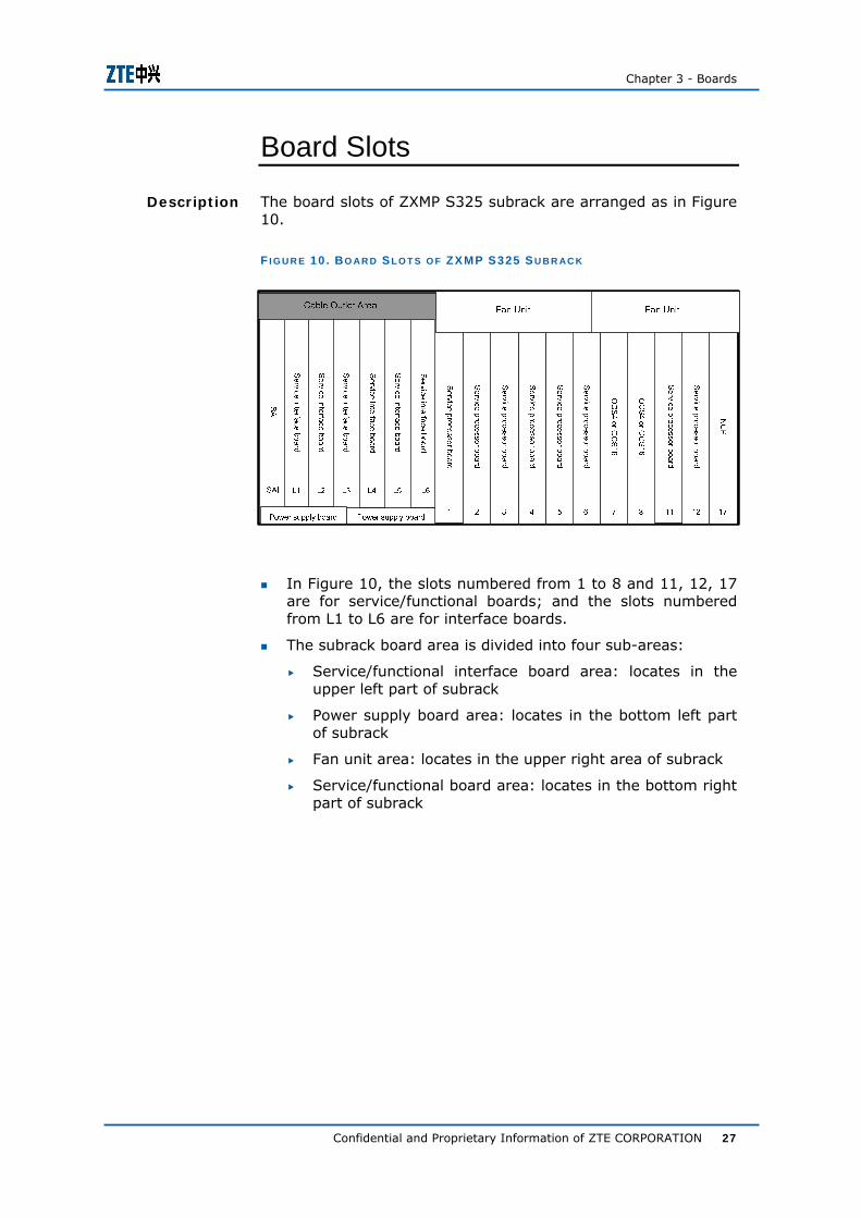
Board Slots
The board slots of ZXMP S325 subrack are arranged as in Figure 10.
F I G U R E 10 . BO AR D S L O T S O F ZXMP S325 S U B R AC K
In Figure 10, the slots numbered from 1 to 8 and 11, 12, 17 are for service/functional boards; and the slots numbered from L1 to L6 are for interface boards.
The subrack board area is divided into four sub-areas:
Service/functional interface board area: locates in the upper left part of subrack
Power supply board area: locates in the bottom left part of subrack
Fan unit area: locates in the upper right area of subrack
Service/functional board area: locates in the bottom right part of subrack
Description
ZXMP S325 (V2.00) Hardware Descriptions
28 Confidential and Proprietary Information of ZTE CORPORATION
Board Structure Functional/Service Interface Board
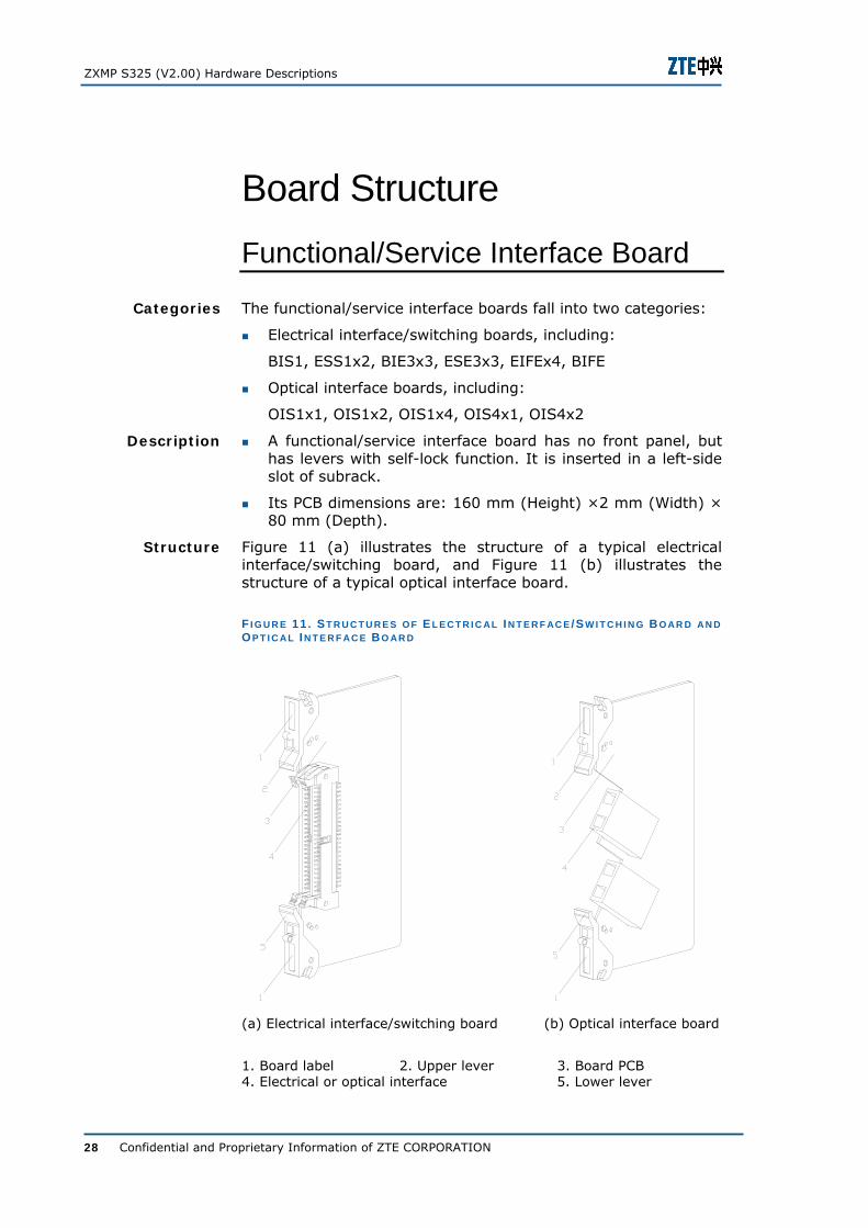
The functional/service interface boards fall into two categories:
Electrical interface/switching boards, including:
BIS1, ESS1x2, BIE3x3, ESE3x3, EIFEx4, BIFE
Optical interface boards, including:
OIS1x1, OIS1x2, OIS1x4, OIS4x1, OIS4x2
A functional/service interface board has no front panel, but has levers with self-lock function. It is inserted in a left-side slot of subrack.
Its PCB dimensions are: 160 mm (Height) ×2 mm (Width) × 80 mm (Depth).
Figure 11 (a) illustrates the structure of a typical electrical interface/switching board, and Figure 11 (b) illustrates the structure of a typical optical interface board.
F I G U R E 11 . ST R U C T U R E S O F E L E C T R I C AL I N T E R F AC E /S W I T C H I N G B O AR D AN D OP T I C AL I N T E R F AC E B O AR D
(a) Electrical interface/switching board (b) Optical interface board
1. Board label 2. Upper lever 3. Board PCB 4. Electrical or optical interface 5. Lower lever
Categories
Description
Structure
Chapter 3 - Boards
Confidential and Proprietary Information of ZTE CORPORATION 29
Notes:
The structures of all the electrical interface/switching boards are similar.
The structures of all optical interface boards are similar.
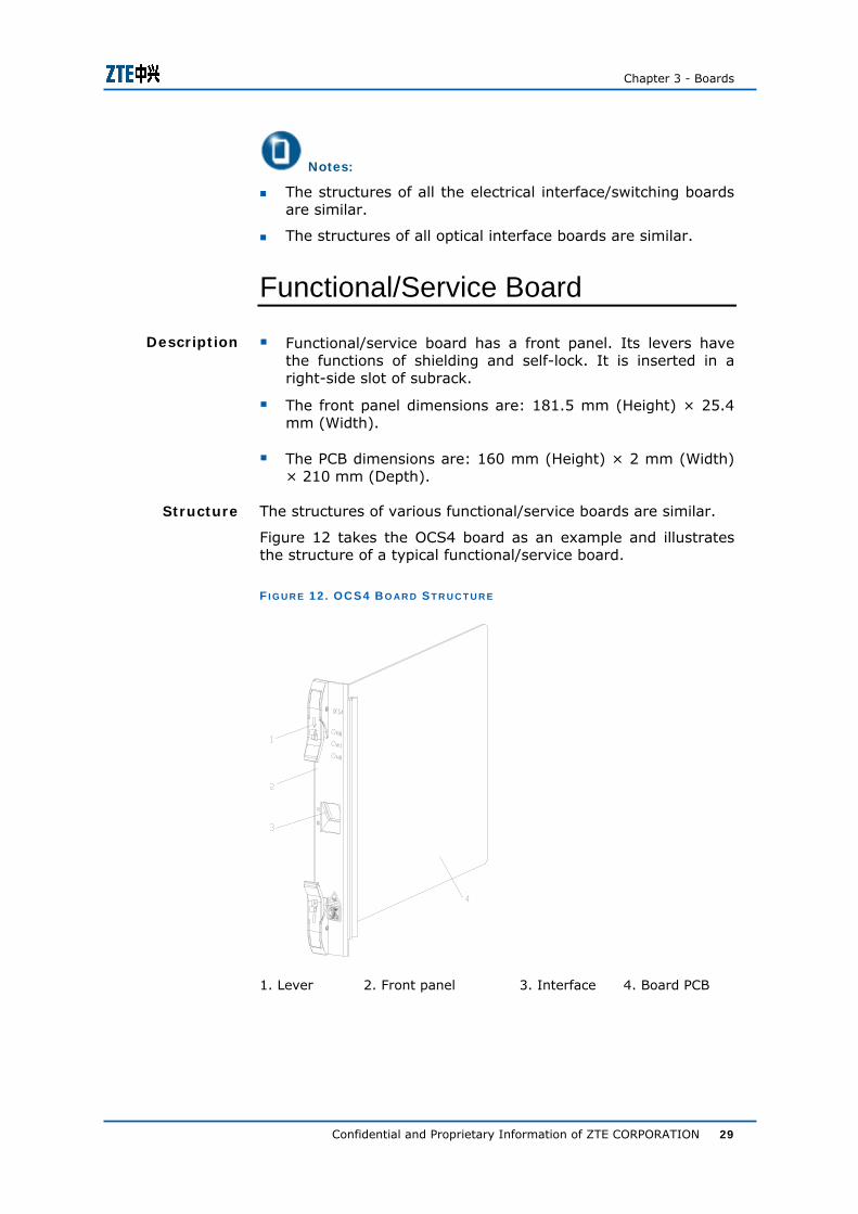
Functional/Service Board
Functional/service board has a front panel. Its levers have the functions of shielding and self-lock. It is inserted in a right-side slot of subrack.
The front panel dimensions are: 181.5 mm (Height) × 25.4 mm (Width).
The PCB dimensions are: 160 mm (Height) × 2 mm (Width) × 210 mm (Depth).
The structures of various functional/service boards are similar.
Figure 12 takes the OCS4 board as an example and illustrates the structure of a typical functional/service board.
F I G U R E 12 . OCS4 B O AR D S T R U C T U R E
1. Lever 2. Front panel 3. Interface 4. Board PCB
Description
Structure
ZXMP S325 (V2.00) Hardware Descriptions
30 Confidential and Proprietary Information of ZTE CORPORATION
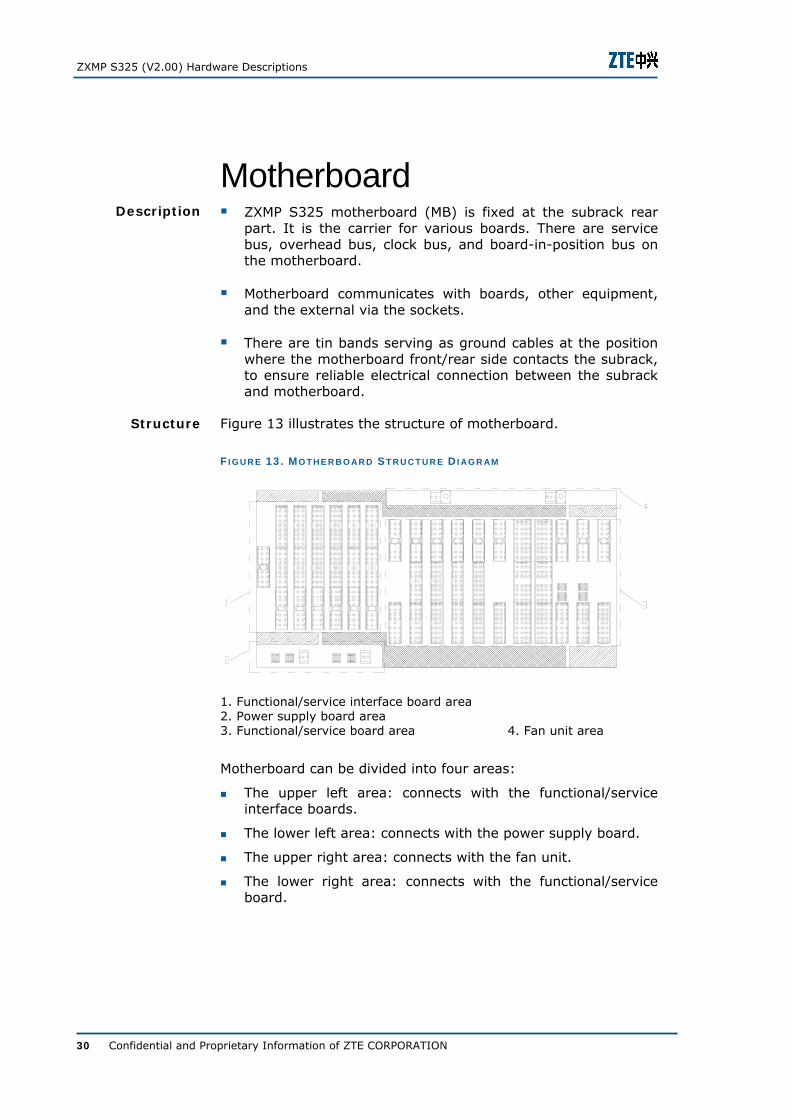
Motherboard ZXMP S325 motherboard (MB) is fixed at the subrack rear
part. It is the carrier for various boards. There are service bus, overhead bus, clock bus, and board-in-position bus on the motherboard.
Motherboard communicates with boards, other equipment, and the external via the sockets.
There are tin bands serving as ground cables at the position where the motherboard front/rear side contacts the subrack, to ensure reliable electrical connection between the subrack and motherboard.
Figure 13 illustrates the structure of motherboard.
F I G U R E 13 . MO T H E R B O AR D S T R U C T U R E D I AG R AM
1. Functional/service interface board area 2. Power supply board area 3. Functional/service board area 4. Fan unit area
Motherboard can be divided into four areas:
The upper left area: connects with the functional/service interface boards.
The lower left area: connects with the power supply board.
The upper right area: connects with the fan unit.
The lower right area: connects with the functional/service board.
Description
Structure
Chapter 3 - Boards
Confidential and Proprietary Information of ZTE CORPORATION 31
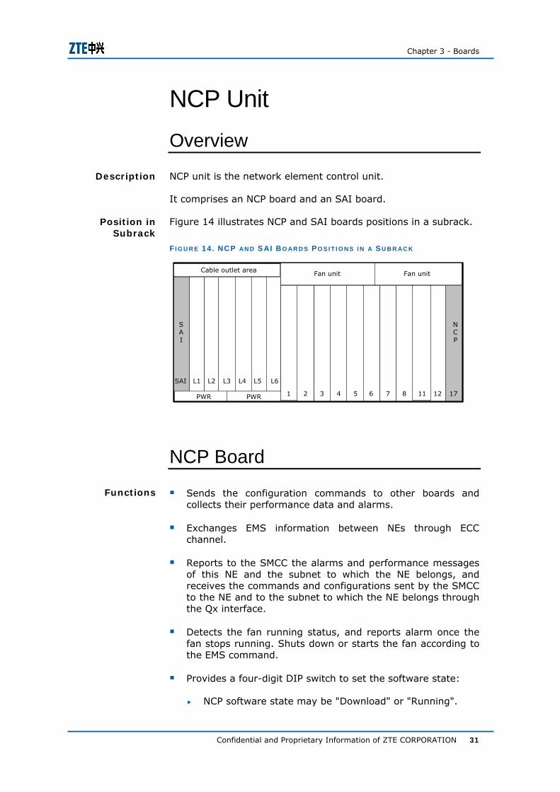
NCP Unit Overview
NCP unit is the network element control unit.
It comprises an NCP board and an SAI board.
Figure 14 illustrates NCP and SAI boards positions in a subrack.
F I G U R E 14 . NCP AN D S AI B O AR D S P O S I T I O N S I N A S U B R AC K
Cable outlet area
PWR PWR 12 177 865432 111
Fan unitFan unit
L6L5L4L3L2L1SAI
NCP
SAI
NCP Board
Sends the configuration commands to other boards and collects their performance data and alarms.
Exchanges EMS information between NEs through ECC channel.
Reports to the SMCC the alarms and performance messages of this NE and the subnet to which the NE belongs, and receives the commands and configurations sent by the SMCC to the NE and to the subnet to which the NE belongs through the Qx interface.
Detects the fan running status, and reports alarm once the fan stops running. Shuts down or starts the fan according to the EMS command.
Provides a four-digit DIP switch to set the software state:
NCP software state may be "Download" or "Running".
Description
Position in Subrack
Functions
ZXMP S325 (V2.00) Hardware Descriptions
32 Confidential and Proprietary Information of ZTE CORPORATION
The Download state: Set the DIP switch to all ON, then NCP board will enter the Download state. It is used to download applications and NCP parameter configuration.
The Running state: Set the DIP switch to not all ON and not all OFF, then NCP board will enter the Running state. It is used to start the NCP board application and makes the NCP board to enter the normal running state.
Following points explain about OW functions of NCP board:
Implements orderwire interworking between NEs via the E1 and E2 bytes.
Provides two voice channels that are independent with each other. The system can support up to 16 orderwire directions.
Achieves calls based on point-to-point, point-to-multipoint, point-to-group, and point-to-the entire line.
Dual tone signaling is adopted for point-to-point calls.
The contact signaling acts as the man-machine interface through the keys on the telephone set, which must be a dual-tone type.
Represents the received dialing and E1/E2 DTMF signaling, decides the channel status according to the signaling, and controls the phone connection.
Following five phone connection states are available:
i. Phone connected to E1 channel
ii. Phone connected to E2 channel
iii. Phone connected to "dial tone & busy tone generating circuit"
iv Phone connected to the ring current signal
v. Free (off-hook and without being called)
Sets orderwire numbers via the EMS
Prevents the orderwire from being looped through EMS settings
The orderwire software can be downloaded online by the EMS
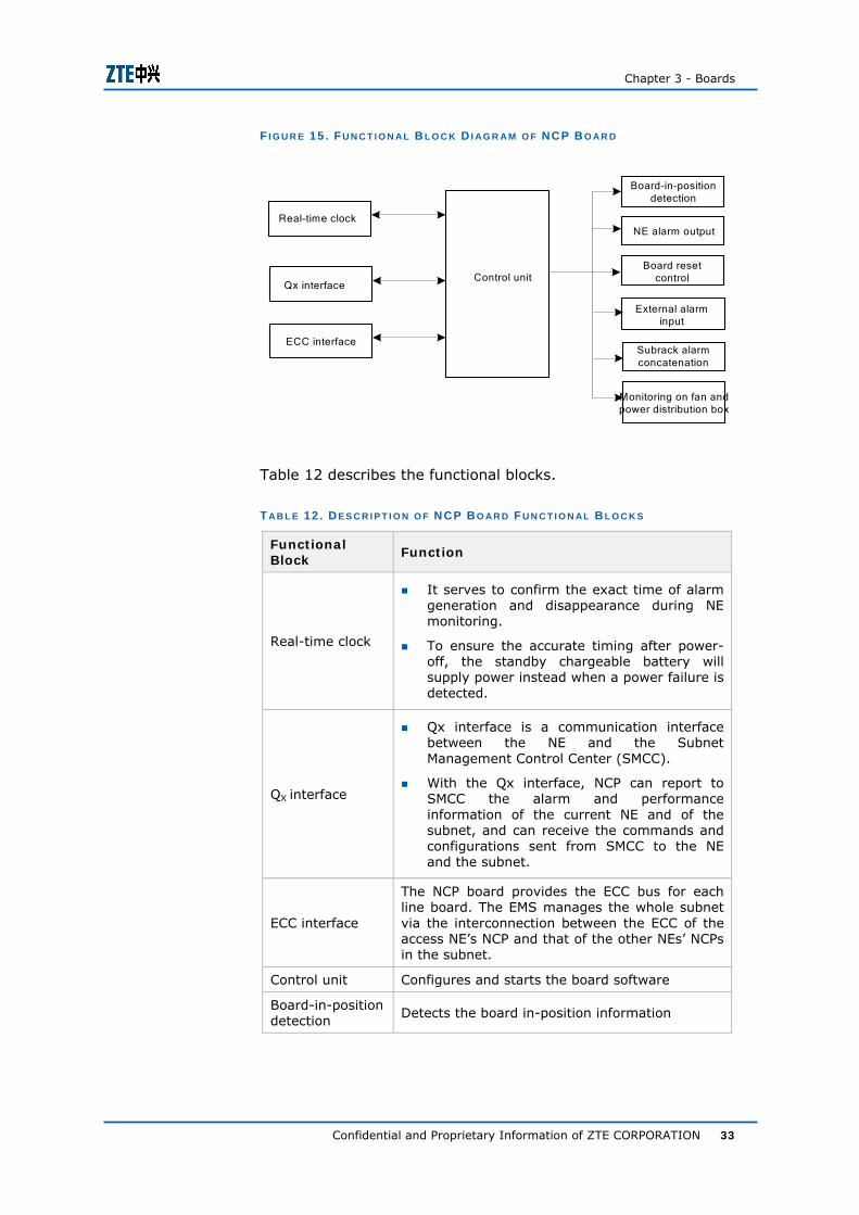
Figure 15 shows the NCP board functional blocks. Functional Blocks
Chapter 3 - Boards
Confidential and Proprietary Information of ZTE CORPORATION 33
F I G U R E 15 . FU N C T I O N AL B L O C K D I AG R A M O F NCP B O A R D
Control unit
Real-time clock
Qx interface
ECC interface
Board-in-position detection
Board reset control
NE alarm output
External alarm input
Monitoring on fan and power distribution box
Subrack alarm concatenation
Table 12 describes the functional blocks.
T AB L E 12 . D E S C R I P T I O N O F NCP B O AR D F U N C T I O N AL B L O C K S
Functional Block
Function
Real-time clock
It serves to confirm the exact time of alarm generation and disappearance during NE monitoring.
To ensure the accurate timing after power-off, the standby chargeable battery will supply power instead when a power failure is detected.
QX interface
Qx interface is a communication interface between the NE and the Subnet Management Control Center (SMCC).
With the Qx interface, NCP can report to SMCC the alarm and performance information of the current NE and of the subnet, and can receive the commands and configurations sent from SMCC to the NE and the subnet.
ECC interface
The NCP board provides the ECC bus for each line board. The EMS manages the whole subnet via the interconnection between the ECC of the access NE’s NCP and that of the other NEs’ NCPs in the subnet.
Control unit Configures and starts the board software
Board-in-position detection
Detects the board in-position information
ZXMP S325 (V2.00) Hardware Descriptions
34 Confidential and Proprietary Information of ZTE CORPORATION
Functional Block
Function
External alarm input, NE alarm output
Monitors external alarms and outputs alarms in the NE
Board reset control
Conducts hard reset of all the boards in the NE
Subrack alarm concatenation
Implements concatenation of alarms from multiple ZXMP S325 subracks
Monitoring on fan and power distribution box
Detects the fan running status, and reports alarm once the fan stops running. Shuts down or starts the fan according to the EMS command.
Detects the over/under-voltage of the subrack power.
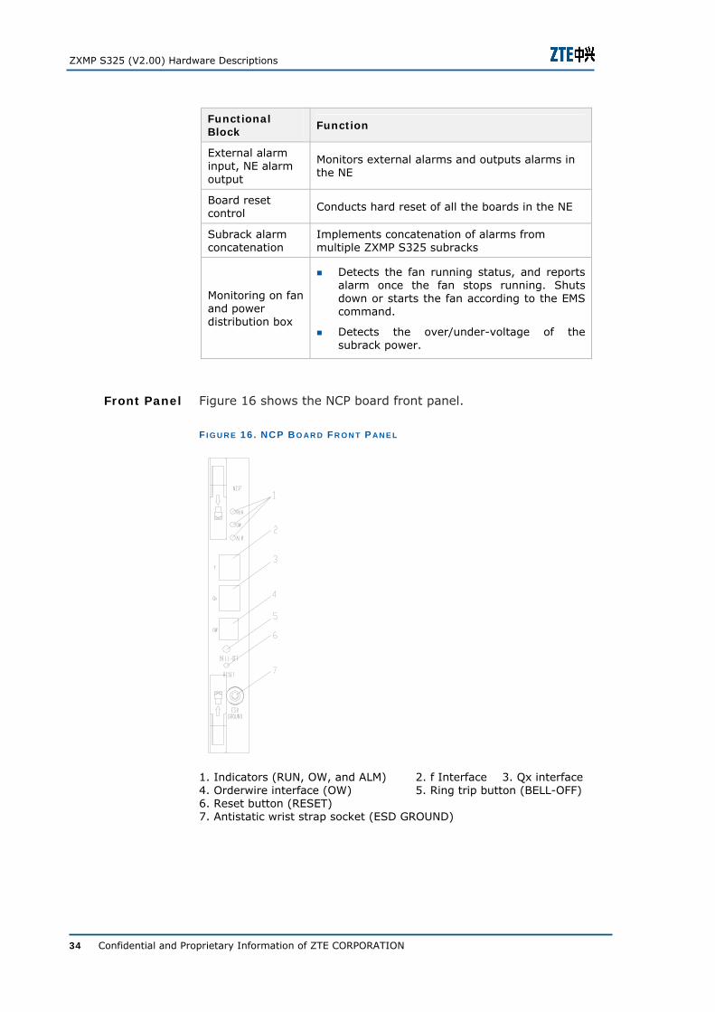
Figure 16 shows the NCP board front panel.
F I G U R E 16 . NCP B O AR D FR O N T P AN E L
1. Indicators (RUN, OW, and ALM) 2. f Interface 3. Qx interface 4. Orderwire interface (OW) 5. Ring trip button (BELL-OFF) 6. Reset button (RESET) 7. Antistatic wrist strap socket (ESD GROUND)
Front Panel
Chapter 3 - Boards
Confidential and Proprietary Information of ZTE CORPORATION 35
Table 13 describes the indicators on the NCP board front panel.
T AB L E 13 . I N D I C AT O R S O N NCP B O AR D F R O N T P AN E L
Indicator Name
Description
RUN Indicator of NCP board working status (green). It flashes periodically when the NCP board is working normally.
OW
Orderwire ringing indicator (red/green).
If the NCP board is working normally, the green indicator flashes periodically. When there is an incoming orderwire call, the red indicator is on.
ALM Alarm indicator (red). It is on when the NCP board detects an alarm. Otherwise, it is off.
Table 14 describes the interfaces and buttons on the NCP board front panel.
T AB L E 14 . I N T E R F AC E S AN D B U T T O N S O N NCP B O AR D F R O N T P AN E L
Name Description
f interface Interface between an NE and portable equipment. Adopts the RJ45 socket
QX interface Communication interface between SMCC and the NE. Adopts the RJ45 socket.
Orderwire interface (OW)
Orderwire interface. Adopts the RJ11 socket
Ring trip button (BELL-OFF)
Controls whether to give a ring alarm
Reset button (RESET) Press down this button to reset the NCP board
Antistatic wrist strap socket (ESD GROUND)
Connects the antistatic wrist strap
Refer to the Overview section of NCP unit.
Indicators
Interfaces and Buttons
Position in Subrack
ZXMP S325 (V2.00) Hardware Descriptions
36 Confidential and Proprietary Information of ZTE CORPORATION
SAI Board
The SAI board communicates with the NCP board and OCS4 board through the motherboard. It provides interfaces for the NCP board and the OCS4 board to connect with the equipment outside.
It provides the NCP board with alarm input and output interfaces, an alarm concatenation interface, and an F1 interface.
It provides the OCS4 board with external clock input and output interfaces.
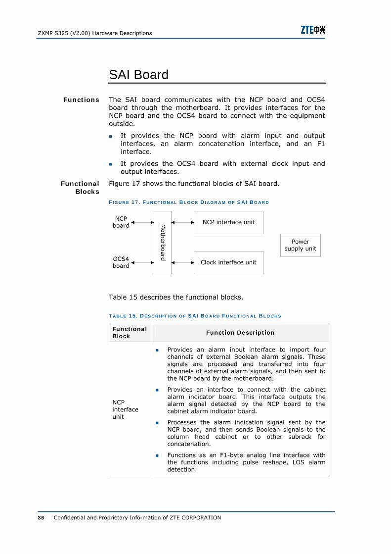
Figure 17 shows the functional blocks of SAI board.
F I G U R E 17 . FU N C T I O N AL B L O C K D I AG R A M O F SAI B O A R D
NCP interface unit
Clock interface unit
Moth
erboard
NCPboard
OCS4board
Powersupply unit
Table 15 describes the functional blocks.
T AB L E 15 . D E S C R I P T I O N O F S AI B O AR D FU N C T I O N AL B L O C K S
Functional Block
Function Description
NCP interface unit
Provides an alarm input interface to import four channels of external Boolean alarm signals. These signals are processed and transferred into four channels of external alarm signals, and then sent to the NCP board by the motherboard.
Provides an interface to connect with the cabinet alarm indicator board. This interface outputs the alarm signal detected by the NCP board to the cabinet alarm indicator board.
Processes the alarm indication signal sent by the NCP board, and then sends Boolean signals to the column head cabinet or to other subrack for concatenation.
Functions as an F1-byte analog line interface with the functions including pulse reshape, LOS alarm detection.
Functions
Functional Blocks
Chapter 3 - Boards
Confidential and Proprietary Information of ZTE CORPORATION 37
Functional Block
Function Description
Clock interface unit
Provides two interfaces to input the 2.048 Mbit/s or 2.048 MHz external clock signal, and two interfaces to output the 2.048 Mbit/s or 2.048 MHz clock signal. Extract the clock and synchronization information.
The DIP switch “S2” on the PCB of SAI board determines whether to input 2.048 Mbit/s or 2.048 MHz clock. If the fourth digit of S2 is set to “ON”, the SAI board inputs/outputs 2.048 MHz clock signal; Otherwise, it inputs/outputs 2.048 Mbit/s clock signal.
Power supply unit
Filters and allocates the power required by the SAI board.
None
None
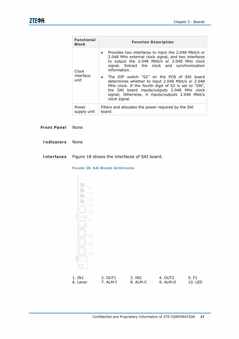
Figure 18 shows the interfaces of SAI board.
F I G U R E 18 . SAI B O AR D I N T E R F AC E S
1. IN1 2. OUT1 3. IN2 4. OUT2 5. F1 6. Lever 7. ALM-I 8. ALM-C 9. ALM-O 10. LED
Front Panel
Indicators
Interfaces
ZXMP S325 (V2.00) Hardware Descriptions
38 Confidential and Proprietary Information of ZTE CORPORATION
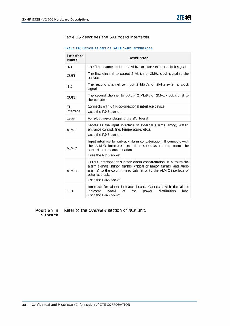
Table 16 describes the SAI board interfaces.
T AB L E 16 . D E S C R I P T I O N S O F SAI B O AR D I N T E R F AC E S
Interface Name Description
IN1 The first channel to input 2 Mbit/s or 2MHz external clock signal
OUT1 The first channel to output 2 Mbit/s or 2MHz clock signal to the outside
IN2 The second channel to input 2 Mbit/s or 2MHz external clock signal
OUT2 The second channel to output 2 Mbit/s or 2MHz clock signal to the outside
F1 interface
Connects with 64 K co-directional interface device. Uses the RJ45 socket.
Lever For plugging/unplugging the SAI board
ALM-I Serves as the input interface of external alarms (smog, water, entrance control, fire, temperature, etc.). Uses the RJ45 socket.
ALM-C
Input interface for subrack alarm concatenation. It connects with the ALM-O interfaces on other subracks to implement the subrack alarm concatenation. Uses the RJ45 socket.
ALM-O
Output interface for subrack alarm concatenation. It outputs the alarm signals (minor alarms, critical or major alarms, and audio alarms) to the column head cabinet or to the ALM-C interface of other subrack. Uses the RJ45 socket.
LED Interface for alarm indicator board. Connects with the alarm indicator board of the power distribution box. Uses the RJ45 socket.
Refer to the Overview section of NCP unit.
Position in Subrack
Chapter 3 - Boards
Confidential and Proprietary Information of ZTE CORPORATION 39
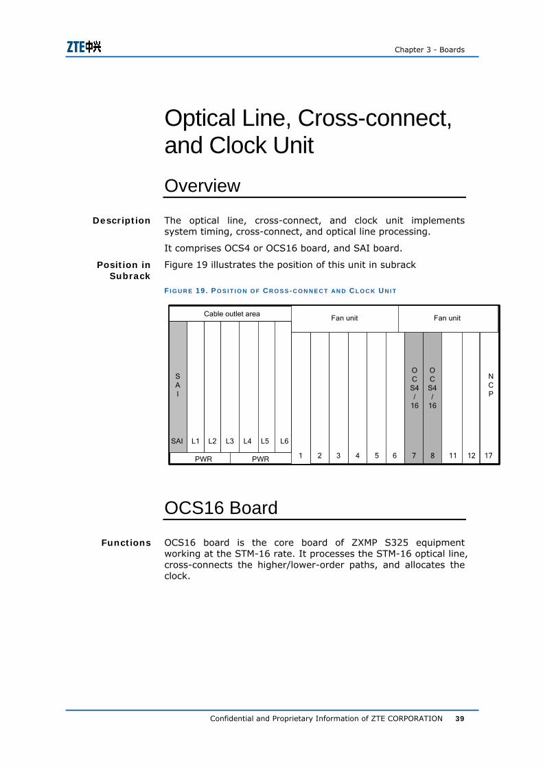
Optical Line, Cross-connect, and Clock Unit Overview
The optical line, cross-connect, and clock unit implements system timing, cross-connect, and optical line processing.
It comprises OCS4 or OCS16 board, and SAI board.
Figure 19 illustrates the position of this unit in subrack
F I G U R E 19 . PO S I T I O N O F CR O S S -C O N N E C T AN D C L O C K U N I T
Cable outlet area
PWR PWR 12 177 865432 111
Fan unitFan unit
L6L5L4L3L2L1SAI
NCP
SAI
OCS4/
16
OCS4/
16
OCS16 Board
OCS16 board is the core board of ZXMP S325 equipment working at the STM-16 rate. It processes the STM-16 optical line, cross-connects the higher/lower-order paths, and allocates the clock.
Description
Position in Subrack
Functions
ZXMP S325 (V2.00) Hardware Descriptions
40 Confidential and Proprietary Information of ZTE CORPORATION
The following points describe OCS4 board functions in detail.
Functions as a clock board
It enables the equipment clock performance to satisfy the clock characteristics specified in the ITU-T G.813 Recommendation.
The system clock supports various work modes including the internal clock, line (or tributary) clock, and external clock.
The system can be configured with ten channels of line (or tributary) clock sources and two channels of external clock sources simultaneously.
The system can perform protection switching among the clock sources according to the alarm and synchronization status information of the clock sources.
It provides the boards in various slots with system clock signal, system frame head signal, and system clock enabling signal.
Employs the software-controlled phase-locking circuit to achieve four work modes as follows:
i. Fast capture mode
ii. Tracing mode
iii. Hold mode
iv. Free-oscillation mode
Implements network-wide clock synchronization via the SSM byte.
Provides the clock for tributary board retiming.
Two OCS16 boards can work in 1+1 hot backup mode in order to ensure the synchronization and timing reliability of clock unit. The standby clock unit traces the frequency and phase of the active clock unit, so that the frequency and phase of the output clock will have no jump when the EMS switches between the active and standby clock unit.
One OCS16 board can also work alone.
Can input two channels of external clock reference and output two channels of clock reference to the outside. The interfaces of these clock references are provided by the SAI board.
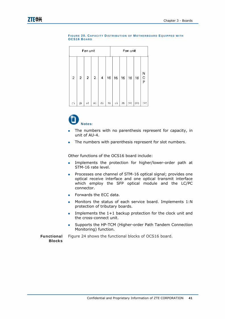
Functions as a cross-connect board
The OCS16 board can cross-connect 92 AU-4s at the higher-order path, and 32 AU-4s at the lower-order path.
When ZXMP S325 is equipped with OCS16 board, the capacity distribution of motherboard is shown in Figure 23.
Chapter 3 - Boards
Confidential and Proprietary Information of ZTE CORPORATION 41
F I G U R E 20 . CAP AC I T Y D I S T R I B U T I O N O F M O T H E R B O AR D E Q U I P P E D W I T H OCS16 B O AR D
Notes:
The numbers with no parenthesis represent for capacity, in unit of AU-4.
The numbers with parenthesis represent for slot numbers.
Other functions of the OCS16 board include:
Implements the protection for higher/lower-order path at STM-16 rate level.
Processes one channel of STM-16 optical signal; provides one optical receive interface and one optical transmit interface which employ the SFP optical module and the LC/PC connector.
Forwards the ECC data.
Monitors the status of each service board. Implements 1:N protection of tributary boards.
Implements the 1+1 backup protection for the clock unit and the cross-connect unit.
Supports the HP-TCM (Higher-order Path Tandem Connection Monitoring) function.
Figure 24 shows the functional blocks of OCS16 board. Functional Blocks
ZXMP S325 (V2.00) Hardware Descriptions
42 Confidential and Proprietary Information of ZTE CORPORATION
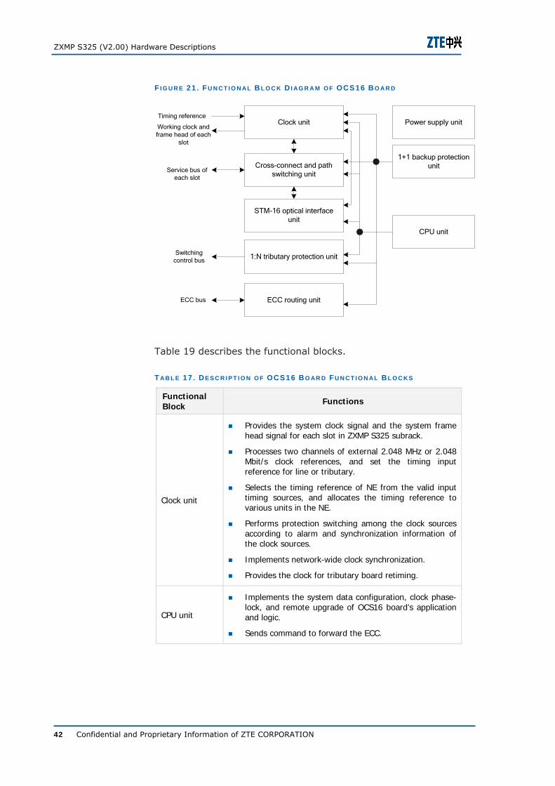
F I G U R E 21 . FU N C T I O N AL B L O C K D I AG R A M O F OCS16 B O AR D
Clock unit
Cross-connect and path switching unit
STM-16 optical interface unit
1:N tributary protection unit
ECC routing unit
Power supply unit
1+1 backup protection unit
CPU unit
Timing reference
Working clock and frame head of each
slot
Service bus of each slot
Switching control bus
ECC bus
Table 19 describes the functional blocks.
T AB L E 17 . D E S C R I P T I O N O F OCS16 B O AR D FU N C T I O N AL B L O C K S
Functional Block Functions
Clock unit
Provides the system clock signal and the system frame head signal for each slot in ZXMP S325 subrack.
Processes two channels of external 2.048 MHz or 2.048 Mbit/s clock references, and set the timing input reference for line or tributary.
Selects the timing reference of NE from the valid input timing sources, and allocates the timing reference to various units in the NE.
Performs protection switching among the clock sources according to alarm and synchronization information of the clock sources.
Implements network-wide clock synchronization.
Provides the clock for tributary board retiming.
CPU unit
Implements the system data configuration, clock phase-lock, and remote upgrade of OCS16 board’s application and logic.
Sends command to forward the ECC.
Chapter 3 - Boards
Confidential and Proprietary Information of ZTE CORPORATION 43
Functional Block Functions
STM-16 optical interface unit
Provides the functions of STM-16 optical interface
Implements the conversion between optical and electrical signals
Separates the data and overhead, and transparently transmits the overhead
Forwards the ECC according to the command sent by the CPU unit and the route found by the ECC routing unit.
Cross-connect and path switching unit
Cross-connects 92 AU-4s at the higher-order path, and 32 AU-4s at the lower-order path.
Implements the path protection
1:N tributary protection unit Implements the 1:N protection for tributary boards.
ECC routing unit Finds route to forward the ECC.
1+1 backup protection unit
Controls the 1+1 backup protection for all the units except the “STM-16 optical interface unit” of OCS16 board.
Power supply unit Filters and allocates the power required by the OCS16 board.
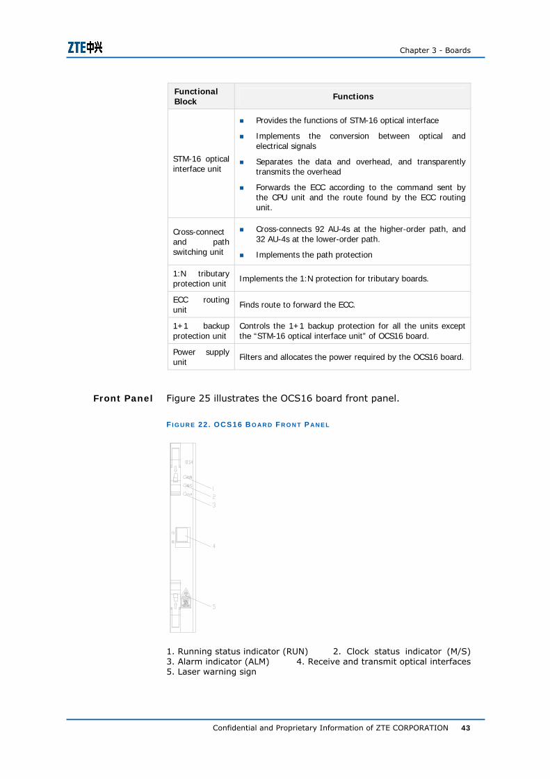
Figure 25 illustrates the OCS16 board front panel.
F I G U R E 22 . OCS16 B O AR D FR O N T P AN E L
1. Running status indicator (RUN) 2. Clock status indicator (M/S) 3. Alarm indicator (ALM) 4. Receive and transmit optical interfaces 5. Laser warning sign
Front Panel
ZXMP S325 (V2.00) Hardware Descriptions
44 Confidential and Proprietary Information of ZTE CORPORATION
Table 20 describes the indicators on OCS16 board front panel.
T AB L E 18 . I N D I C AT O R S O N OCS16 B O AR D FR O N T P AN E L
Indicator Name
Description
RUN Indicator of board working status (green). It flashes periodically and slowly when the board is working normally.
M/S
Indicator of clock status (green). Its states are:
Flashes in the frequency of 5 Hz if the clock works in the fast capture mode
Flashes in the frequency of 1 Hz if the clock works in the tracing mode
Flashes in the frequency of 0.5 Hz if the clock works in the free-oscillation mode
It is on if the clock works in the hold mode
It is off if the board is in standby mode
ALM Alarm indicator (red). It is on when the board detects an alarm. Otherwise, it is off.
RX: the optical receive interface.
TX: the optical transmit interface.
Note: The connector type of these interfaces is LC/PC.
Laser warning sign: Warns the operator not to look straight at the optical interface when plugging/unplugging the fiber pigtail lest the eyes would be burnt.
Refer to the Overview section of the optical line, cross-connect, and clock Unit.
The optical line, clock, and cross-connect functions of OCS16 board are managed by different modules in the EMS. Refer to the ZXONM E300 manuals for operation details.
Refer to the section of SAI Board in Chapter 3 for its functions, functional blocks, and interfaces.
Indicators
Interfaces and Sign
Position in Subrack
Related Information
Chapter 3 - Boards
Confidential and Proprietary Information of ZTE CORPORATION 45
OCS4 Board
OCS4 board is the core board of ZXMP S325 equipment working at the STM-1/STM-4 rate. It processes the STM-1/STM-4 optical line, cross-connects the higher/lower-order paths, and allocates the clock.
Note: Whether the rate of OCS4 board is STM-1 or STM-4 is determined by the optical module installed in the OCS4 board.
The following points describe OCS4 board functions in detail.
Functions as a clock board
It enables the equipment clock performance to satisfy the clock characteristics specified in the ITU-T G.813 Recommendation.
The system clock supports various work modes including the internal clock, line (or tributary) clock, and external clock.
The system can be configured with eight channels of line (or tributary) clock sources and two channels of external clock sources simultaneously.
The system can perform protection switching among the clock sources according to the alarm and synchronization status information of the clock sources.
It provides the boards in various slots with system clock signal, system frame head signal, and system clock enabling signal.
Employs the software-controlled phase-locking circuit to achieve four work modes as follows:
i. Fast capture mode
ii. Tracing mode
iii. Hold mode
iv. Free-oscillation mode
Implements network-wide clock synchronization via the SSM byte.
Provides the clock for tributary board retiming.
Two OCS4 boards can work in 1+1 hot backup mode in order to ensure the synchronization and timing reliability of clock unit. The standby clock unit traces the frequency and phase of the active clock unit, so that the frequency and phase of the output clock will have no jump when the EMS switches between the active and standby clock unit.
One OCS4 board can also work alone.
Functions
ZXMP S325 (V2.00) Hardware Descriptions
46 Confidential and Proprietary Information of ZTE CORPORATION
Can input two channels of external clock reference and output two channels of clock reference to the outside. The interfaces of these clock references are provided by the SAI board.
Functions as a cross-connect board
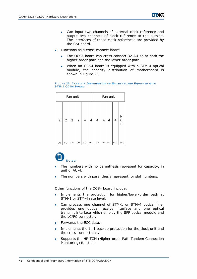
The OCS4 board can cross-connect 32 AU-4s at both the higher-order path and the lower-order path.
When an OCS4 board is equipped with a STM-4 optical module, the capacity distribution of motherboard is shown in Figure 23.
F I G U R E 23 . CAP AC I T Y D I S T R I B U T I O N O F M O T H E R B O AR D E Q U I P P E D W I T H STM-4 OCS4 B O AR D
NCP
(2)(1)
Fan unitFan unit
(3) (4) (5) (6) (7) (8) (11) (12) (17)
2 2 2 2 4 4 4 4 4 4
Notes:
The numbers with no parenthesis represent for capacity, in unit of AU-4.
The numbers with parenthesis represent for slot numbers.
Other functions of the OCS4 board include:
Implements the protection for higher/lower-order path at STM-1 or STM-4 rate level.
Can process one channel of STM-1 or STM-4 optical line; provides one optical receive interface and one optical transmit interface which employ the SFP optical module and the LC/PC connector.
Forwards the ECC data.
Implements the 1+1 backup protection for the clock unit and the cross-connect unit.
Supports the HP-TCM (Higher-order Path Tandem Connection Monitoring) function.
Chapter 3 - Boards
Confidential and Proprietary Information of ZTE CORPORATION 47
Figure 24 shows the functional blocks of OCS4 board.
F I G U R E 24 . FU N C T I O N AL B L O C K D I AG R A M O F OCS4 BO AR D
Clock unit
Cross-connect and pathswitching unit
STM-1/STM-4 opticalinterface unit
1:N tributary protectionunit
ECC routing unit
Power supply unit
1+1 backupprotection unit
CPU unit
Timing reference
Working clock andframe head of
each slot
Service busof each slot
Switchingcontrol bus
ECC bus
Table 19 describes the functional blocks.
T AB L E 19 . D E S C R I P T I O N O F OCS4 B O AR D FU N C T I O N AL B L O C K S
Functional Block Functions
Clock unit
Provides the system clock signal and the system frame head signal for each slot in ZXMP S325 subrack.
Processes two channels of external 2.048 MHz or 2.048 Mbit/s clock references, and set the timing input reference for line or tributary.
Selects the timing reference of NE from the valid input timing sources, and allocates the timing reference to various units in the NE.
Performs protection switching among the clock sources according to alarm and synchronization information of the clock sources.
Implements network-wide clock synchronization.
Provides the clock for tributary board retiming.
CPU unit
Implements the system data configuration, the clock phase-lock, the remote upgrade of OCS4 board’s application and logic.
Sends command to forward the ECC.
Functional Blocks
ZXMP S325 (V2.00) Hardware Descriptions
48 Confidential and Proprietary Information of ZTE CORPORATION
Functional Block Functions
STM-1/STM-4 optical interface unit
Provides the functions of STM-1 or STM-4 optical interface
Implements the conversion between optical and electrical signals
Separates the data and overhead, and transparently transmits the overhead
Forwards the ECC according to the command sent by the CPU unit and the route found by the ECC routing unit.
Cross-connect and path switching unit
Cross-connects 32 AU-4s at both the higher-order path and the lower-order path.
Implements the path protection
1:N tributary protection unit Implements the 1:N protection for tributary boards.
ECC routing unit Finds route to forward the ECC.
1+1 backup protection unit
Controls the 1+1 backup protection for all the units except the “STM-1/STM-4 optical interface unit” in the OCS4 board.
Power supply unit Filters and allocates the power required by the OCS4 board.
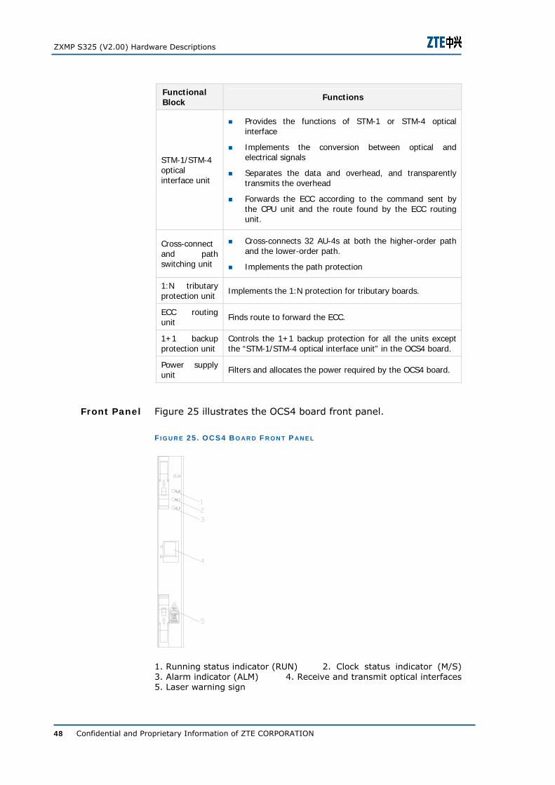
Figure 25 illustrates the OCS4 board front panel.
F I G U R E 25 . OCS4 B O AR D F R O N T P AN E L
1. Running status indicator (RUN) 2. Clock status indicator (M/S) 3. Alarm indicator (ALM) 4. Receive and transmit optical interfaces 5. Laser warning sign
Front Panel
Chapter 3 - Boards
Confidential and Proprietary Information of ZTE CORPORATION 49
Table 20 describes the indicators on OCS4 board front panel.
T AB L E 20 . I N D I C AT O R S O N OCS4 B O AR D FR O N T P AN E L
Indicator Name
Description
RUN Indicator of board working status (green). It flashes periodically and slowly when the board is working normally.
M/S
Indicator of clock status (green). Its states are:
Flashes in the frequency of 5 Hz if the clock works in the fast capture mode
Flashes in the frequency of 1 Hz if the clock works in the tracing mode
Flashes in the frequency of 0.5 Hz if the clock works in the free-oscillation mode
It is on if the clock works in the hold mode
It is off if the board is in standby mode
ALM Alarm indicator (red). It is on when the board detects an alarm. Otherwise, it is off.
RX: the optical receive interface.
TX: the optical transmit interface.
Note: The connector type of these interfaces is LC/PC.
Laser warning sign: Warns the operator not to look straight at the optical interface when plugging/unplugging the fiber pigtail lest the eyes would be burnt.
Refer to the Overview section of the optical line, cross-connect, and clock Unit.
The optical line, clock, and cross-connect functions of OCS4 board are managed by different modules in the EMS. Refer to the ZXONM E300 manuals for operation details.
Refer to the section of SAI Board in Chapter 3 for its functions, functional blocks, and interfaces.
Indicators
Interfaces and Sign
Position in Subrack
Related Information
ZXMP S325 (V2.00) Hardware Descriptions
50 Confidential and Proprietary Information of ZTE CORPORATION
OL16x1 Board OL16x1 board provides one pair of STM-16 standard optical
transmit/receive interfaces.
Terminates and regenerates the STM-16 regenerator section overhead and multiplex section overhead.
Interprets the AU-4 pointer and obtains the VC payload.
Forwards EMS information from optical line board to NCP board.
Outputs the received reference clock to OCS16 board.
Forwards ECC data.
Supports query of parameters of four optical modules: optical received power module, optical launched power module, temperature module, and laser working current module.
Supports color optical interface.
Supports online query of optical module type.
Supports HP-TCM (Higher-order Path Tandem Connection Monitoring) function. On the border of different carriers’ networks, it can detect the number of B3 block errors received by this network, as well as the number of B3 block errors sent from this network to next network.
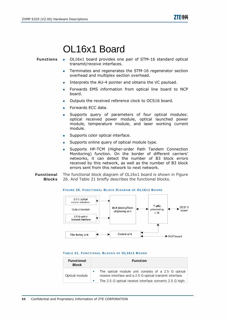
The functional block diagram of OL16x1 board is shown in Figure 26. And Table 21 briefly describes the functional blocks.
F I G U R E 26 . FU N C T I O N AL B L O C K D I AG R A M O F OL16 X 1 B O AR D
T AB L E 21 . FU N C T I O N AL B L O C K S O F OL16 X 1 B O AR D
Functional Block
Function
Optical module The optical module unit consists of a 2.5 G optical
receive interface and a 2.5 G optical transmit interface. The 2.5 G optical receive interface converts 2.5 G high-
Functions
Functional Blocks
Chapter 3 - Boards
Confidential and Proprietary Information of ZTE CORPORATION 51
Functional Block
Function
speed optical signal into electrical signal. It can also monitor the optical received power.
The 2.5 G optical transmit interface converts electrical signal into 2.5 G high-speed optical signal. It can also shut down the laser; monitor the optical launched power and the laser working current.
Multiplexing /Demultiplexing unit
Extracts clock at the receive direction, multiplies frequency of clock at the transmit direction, demultiplexes data at the receive direction, and multiplexes data at the transmit direction.
Control unit
Provides interfaces and channels via which it can communicate with NCP board to perform such functions as performance statistics, alarm detection, temperature control, status setting, and inter-board communications.
Traffic processing unit
Separates payload from overhead, and combines payload with overhead.
Extracts and inserts section overhead (SOH). Processes pointers, alarms, and ECC forwarding;
implements bit error statistics.
Monitoring unit Performs various monitoring functions, such as temperature detection.
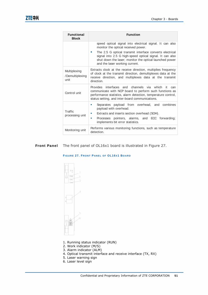
The front panel of OL16x1 board is illustrated in Figure 27.
F I G U R E 27 . FR O N T P AN E L O F OL16 X 1 BO AR D
1. Running status indicator (RUN) 2. Work indicator (M/S) 3. Alarm indicator (ALM) 4. Optical transmit interface and receive interface (TX, RX) 5. Laser warning sign 6. Laser level sign
Front Panel
ZXMP S325 (V2.00) Hardware Descriptions
52 Confidential and Proprietary Information of ZTE CORPORATION
There are three indicators on the front panel, which are in turn the RUN (green) indicator, the M/S (green) indicator, and the ALM (red) indicator from top to bottom.
The RUN indicator flickers slowly and regularly if the board is running normally.
The M/S indicator is ON if the board is running normally.
The ALM indicator is OFF if the board has no alarm; otherwise, it is ON.
OL16x1 board provides one optical receive interface (RX) and one optical transmit interface (TX). They receive or transmit STM-16 optical signals. Their connectors are both LC/PC type.
The laser warning sign warns the operator not to look straight at optical interface when plugging/unplugging fiber pigtail, lest eyes would be hurt.
The laser level sign marks the laser level.
OL16x1 board cannot work unless OCS16 board is installed. With OCS16 board installed, OL16x1 board can be inserted in slot 6, 11, and 12.
The grey part in Figure 28 illustrates the position of OL16x1 board in ZXMP S325 subrack.
F I G U R E 28 . PO S I T I O N O F OL16 X 1 B O AR D I N S U B R AC K
Cable outlet area
PWR PWR 12 177 865432 111
Fan unitFan unit
L6L5L4L3L2L1SAI
NCP
SAI
OCS4/
16
OCS4/
16
Indicators
Interfaces and Signs
Position in Subrack
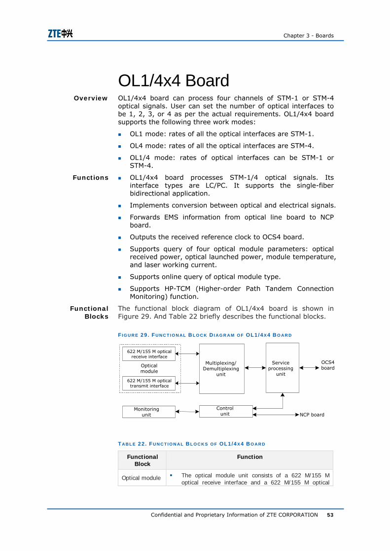
Chapter 3 - Boards
Confidential and Proprietary Information of ZTE CORPORATION 53
OL1/4x4 Board OL1/4x4 board can process four channels of STM-1 or STM-4 optical signals. User can set the number of optical interfaces to be 1, 2, 3, or 4 as per the actual requirements. OL1/4x4 board supports the following three work modes:
OL1 mode: rates of all the optical interfaces are STM-1.
OL4 mode: rates of all the optical interfaces are STM-4.
OL1/4 mode: rates of optical interfaces can be STM-1 or STM-4.
OL1/4x4 board processes STM-1/4 optical signals. Its interface types are LC/PC. It supports the single-fiber bidirectional application.
Implements conversion between optical and electrical signals.
Forwards EMS information from optical line board to NCP board.
Outputs the received reference clock to OCS4 board.
Supports query of four optical module parameters: optical received power, optical launched power, module temperature, and laser working current.
Supports online query of optical module type.
Supports HP-TCM (Higher-order Path Tandem Connection Monitoring) function.
The functional block diagram of OL1/4x4 board is shown in Figure 29. And Table 22 briefly describes the functional blocks.
F I G U R E 29 . FU N C T I O N AL B L O C K D I AG R A M O F OL1/4 X 4 B O AR D
Multiplexing/Demultiplexing
unit622 M/155 M opticaltransmit interface
Monitoringunit NCP board
OCS4board
Serviceprocessing
unit
Controlunit
Opticalmodule
622 M/155 M opticalreceive interface
T AB L E 22 . FU N C T I O N AL B L O C K S O F OL1/4 X 4 B O AR D
Functional Block
Function
Optical module The optical module unit consists of a 622 M/155 M optical receive interface and a 622 M/155 M optical
Overview
Functions
Functional Blocks
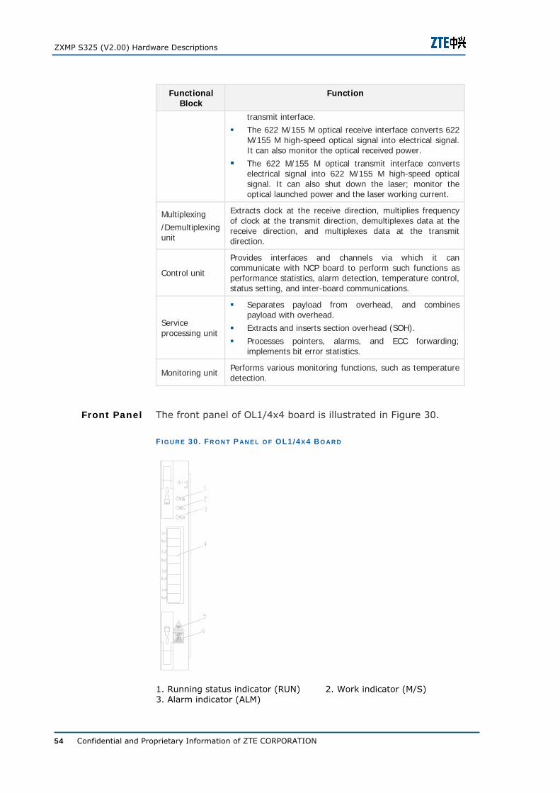
ZXMP S325 (V2.00) Hardware Descriptions
54 Confidential and Proprietary Information of ZTE CORPORATION
Functional Block
Function
transmit interface. The 622 M/155 M optical receive interface converts 622
M/155 M high-speed optical signal into electrical signal. It can also monitor the optical received power.
The 622 M/155 M optical transmit interface converts electrical signal into 622 M/155 M high-speed optical signal. It can also shut down the laser; monitor the optical launched power and the laser working current.
Multiplexing /Demultiplexing unit
Extracts clock at the receive direction, multiplies frequency of clock at the transmit direction, demultiplexes data at the receive direction, and multiplexes data at the transmit direction.
Control unit
Provides interfaces and channels via which it can communicate with NCP board to perform such functions as performance statistics, alarm detection, temperature control, status setting, and inter-board communications.
Service processing unit
Separates payload from overhead, and combines payload with overhead.
Extracts and inserts section overhead (SOH). Processes pointers, alarms, and ECC forwarding;
implements bit error statistics.
Monitoring unit Performs various monitoring functions, such as temperature detection.
The front panel of OL1/4x4 board is illustrated in Figure 30.
F I G U R E 30 . FR O N T P AN E L O F OL1/4 X 4 B O AR D
1. Running status indicator (RUN) 2. Work indicator (M/S) 3. Alarm indicator (ALM)
Front Panel
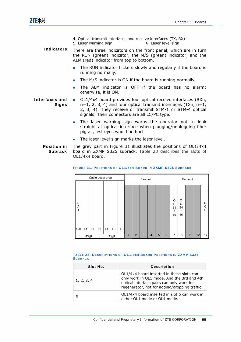
Chapter 3 - Boards
Confidential and Proprietary Information of ZTE CORPORATION 55
4. Optical transmit interfaces and receive interfaces (TX, RX) 5. Laser warning sign 6. Laser level sign
There are three indicators on the front panel, which are in turn the RUN (green) indicator, the M/S (green) indicator, and the ALM (red) indicator from top to bottom.
The RUN indicator flickers slowly and regularly if the board is running normally.
The M/S indicator is ON if the board is running normally.
The ALM indicator is OFF if the board has no alarm; otherwise, it is ON.
OL1/4x4 board provides four optical receive interfaces (RXn, n=1, 2, 3, 4) and four optical transmit interfaces (TXn, n=1, 2, 3, 4). They receive or transmit STM-1 or STM-4 optical signals. Their connectors are all LC/PC type.
The laser warning sign warns the operator not to look straight at optical interface when plugging/unplugging fiber pigtail, lest eyes would be hurt.
The laser level sign marks the laser level.
The grey part in Figure 31 illustrates the positions of OL1/4x4 board in ZXMP S325 subrack. Table 23 describes the slots of OL1/4x4 board.
F I G U R E 31 . PO S I T I O N S O F OL1/4 X 4 B O AR D I N ZXMP S325 S U B R AC K
Cable outlet area
PWR PWR 12 177 865432 111
Fan unitFan unit
L6L5L4L3L2L1SAI
NCP
SAI
OCS4/
16
OCS4/
16
T AB L E 23 . D E S C R I P T I O N S O F OL1/4 X 4 BO AR D P O S I T I O N S I N ZXMP S325 S U B R AC K
Slot No. Description
1, 2, 3, 4
OL1/4x4 board inserted in these slots can only work in OL1 mode. And the 3rd and 4th optical interface pairs can only work for regenerator, not for adding/dropping traffic.
5 OL1/4x4 board inserted in slot 5 can work in either OL1 mode or OL4 mode.
Indicators
Interfaces and Signs
Position in Subrack
ZXMP S325 (V2.00) Hardware Descriptions
56 Confidential and Proprietary Information of ZTE CORPORATION
Slot No. Description
When working in OL4 mode, the 2nd, 3rd and 4th optical interface pairs can only work for regenerator, not for adding/dropping traffic.
If OCS4 board is installed, OL1/4x4 board can work in either OL1 mode or OL4 mode.
When working in OL4 mode, the 2nd, 3rd and 4th optical interface pairs can only work for regenerator, not for adding/dropping traffic.
6, 11, 12
If OCS16 board is installed, OL1/4x4 board can work in OL1 mode, OL4 mode, or OL1/4 mode.
Note: If all the optical interfaces of OL1/4x4 board work for regenerator, the OL1/4x4 board can be inserted in any service board slot.
Chapter 3 - Boards
Confidential and Proprietary Information of ZTE CORPORATION 57
OL1/4 Subsystem Overview
Implements the functions of STM-1 electrical interface, and STM-1/STM-4 optical interface.
Implements conversion between optical and electrical signals.
Separates overhead from data
Provides 1:N (N≤5) protection for STM-1 electrical interface.
The OL1/4 subsystem comprises the following boards:
LP1x1, LP1x2, LP4x1, LP4x2, OIS1x1, OIS1x2, OIS4x1, OIS4x2, ESS1x2, BIS1
Table 24 illustrates boards with different combinations to implement the different functions.
T AB L E 24 . B O A R D C O M B I N AT I O N S I N OL1/4 S U B S Y S T E M
Function Boards Involved
STM-1 optical interface function
LP1x1 (or LP1x2), OIS1x1 (or OIS1x2)
STM-1 electrical interface function
LP1x1 (or LP1x2), ESS1x2
STM-1 electrical interface function with 1:N protection
LP1x1 (or LP1x2), ESS1x2, BIS1
STM-4 optical interface function
LP4x1, OIS4x1, LP4x2, OIS4x2
The positions of boards in the OL1/4 subsystem are filled gray in Figure 32.
Subsystem Functions
Composition
Position in Subrack
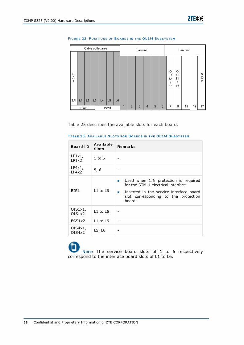
ZXMP S325 (V2.00) Hardware Descriptions
58 Confidential and Proprietary Information of ZTE CORPORATION
F I G U R E 32 . PO S I T I O N S O F B O AR D S I N T H E OL1/4 S U B S Y S T E M
Cable outlet area
PWR PWR 12 177 865432 111
Fan unitFan unit
L6L5L4L3L2L1SAI
NCP
SAI
OCS4/
16
OCS4/
16
Table 25 describes the available slots for each board.
T AB L E 25 . AV A I L A B L E S L O T S F O R B O AR D S I N T H E OL1/4 S U B S Y S T E M
Board ID Available Slots
Remarks
LP1x1, LP1x2
1 to 6 -
LP4x1, LP4x2
5, 6 -
BIS1 L1 to L6
Used when 1:N protection is required for the STM-1 electrical interface
Inserted in the service interface board slot corresponding to the protection board.
OIS1x1, OIS1x2
L1 to L6 -
ESS1x2 L1 to L6 -
OIS4x1, OIS4x2
L5, L6 -
Note: The service board slots of 1 to 6 respectively correspond to the interface board slots of L1 to L6.
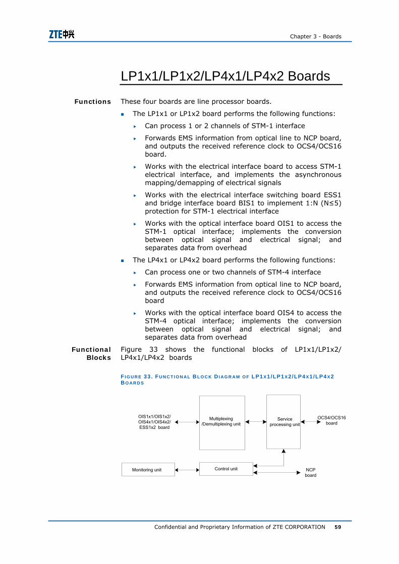
Chapter 3 - Boards
Confidential and Proprietary Information of ZTE CORPORATION 59
LP1x1/LP1x2/LP4x1/LP4x2 Boards
These four boards are line processor boards.
The LP1x1 or LP1x2 board performs the following functions:
Can process 1 or 2 channels of STM-1 interface
Forwards EMS information from optical line to NCP board, and outputs the received reference clock to OCS4/OCS16 board.
Works with the electrical interface board to access STM-1 electrical interface, and implements the asynchronous mapping/demapping of electrical signals
Works with the electrical interface switching board ESS1 and bridge interface board BIS1 to implement 1:N (N≤5) protection for STM-1 electrical interface
Works with the optical interface board OIS1 to access the STM-1 optical interface; implements the conversion between optical signal and electrical signal; and separates data from overhead
The LP4x1 or LP4x2 board performs the following functions:
Can process one or two channels of STM-4 interface
Forwards EMS information from optical line to NCP board, and outputs the received reference clock to OCS4/OCS16 board
Works with the optical interface board OIS4 to access the STM-4 optical interface; implements the conversion between optical signal and electrical signal; and separates data from overhead
Figure 33 shows the functional blocks of LP1x1/LP1x2/ LP4x1/LP4x2 boards
F I G U R E 33 . FU N C T I O N AL B L O C K D I AG R A M O F LP1 X1 /LP1 X 2 /LP4 X 1 /LP4 X 2 B O AR D S
Multiplexing/Demultiplexing unit
OIS1x1/OIS1x2/ OIS4x1/OIS4x2/ESS1x2 board
Monitoring unit NCP board
OCS4/OCS16 board
Service processing unit
Control unit
Functions
Functional Blocks
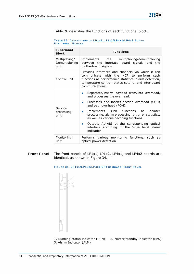
ZXMP S325 (V2.00) Hardware Descriptions
60 Confidential and Proprietary Information of ZTE CORPORATION
Table 26 describes the functions of each functional block.
T AB L E 26 . D E S C R I P T I O N O F LP1 X 1 /LP1 X 2/LP4 X 1 /LP4 X2 B O AR D FU N C T I O N AL B L O C K S
Functional Block
Functions
Multiplexing/ Demultiplexing unit
Implements the multiplexing/demultiplexing between the interface board signals and the motherboard signals.
Control unit
Provides interfaces and channels via which it can communicate with the NCP to perform such functions as performance statistics, alarm detection, temperature control, status setting, and inter-board communications.
Service processing unit
Separates/inserts payload from/into overhead, and processes the overhead.
Processes and inserts section overhead (SOH) and path overhead (POH).
Implements such functions as pointer processing, alarm processing, bit error statistics, as well as various decoding functions.
Outputs AU-AIS at the corresponding optical interface according to the VC-4 level alarm indication.
Monitoring unit
Performs various monitoring functions, such as optical power detection
The front panels of LP1x1, LP1x2, LP4x1, and LP4x2 boards are identical, as shown in Figure 34.
F I G U R E 34 . LP1 X 1 /LP1 X 2 /LP4 X 1 /LP4 X 2 B O AR D FR O N T P AN E L
1. Running status indicator (RUN) 2. Master/standby indicator (M/S) 3. Alarm Indicator (ALM)
Front Panel
Chapter 3 - Boards
Confidential and Proprietary Information of ZTE CORPORATION 61
Table 27 describes the indicators on the front panel.
T AB L E 27 . I N D I C AT O R S O N T H E LP1 X 1/LP1 X 2 /LP4 X 1 B O AR D FR O N T P AN E L
Indicator Name
Description
RUN Running status indicator (green). It flashes periodically and slowly if the board is running normally.
M/S
Master/standby indicator (green). It is on if the board is in active status. It is off if the board is in standby status. When there is no board protection, it is on if the board works normally.
ALM Alarm Indicator (red). It is off if the board detects no alarm. It is on if the board detects alarm.
None
Refer to the Overview section of the OL1/4 subsystem.
OIS1x1/OIS1x2/OIS4x1/OIS4x2 Boards
These boards are optical interface boards.
OIS1x1 or OIS1x2 board performs the following functions:
OISx1 board provides one STM-1 optical receive interface and one STM-1 optical transmit interface.
OIS1x2 board provides two STM-1 optical receive interfaces and two STM-1 optical transmit interfaces.
The optical transmit interface can automatically shut down the laser.
OIS4x1 or OIS4x2 board performs the following functions:
OIS4x1 board provides one STM-4 optical receive interface and one STM-4 optical transmit interface.
OIS4x2 board provides two STM-4 optical receive interface and two STM-4 optical transmit interface.
The optical transmit interface can automatically shut down the laser.
These boards have the same working principle:
At the receive side, the board receives the optical signal inputted from the outside. Then it converts the 622 Mbit/s or 155 Mbit/s optical signal into electrical signal and extracts the line signal. Finally, it sends the processed electrical signal
Indicators
Interface
Position in Subrack
Functions
Working Principle
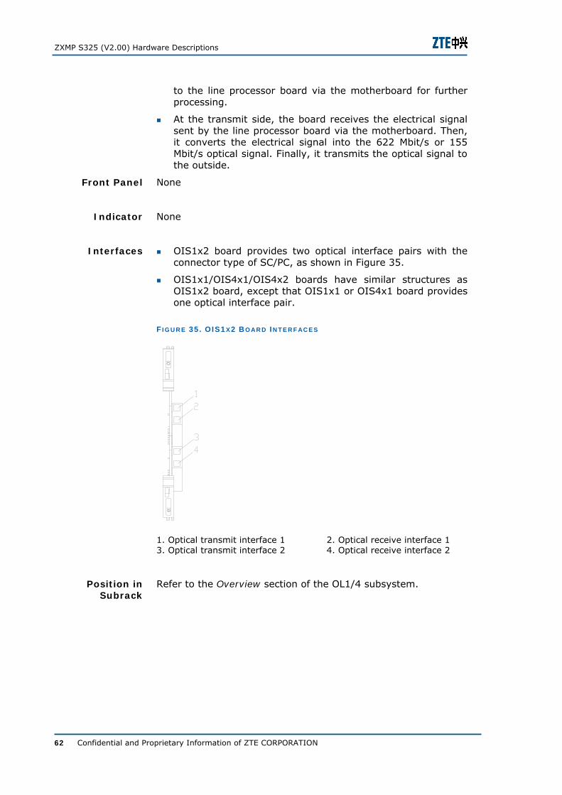
ZXMP S325 (V2.00) Hardware Descriptions
62 Confidential and Proprietary Information of ZTE CORPORATION
to the line processor board via the motherboard for further processing.
At the transmit side, the board receives the electrical signal sent by the line processor board via the motherboard. Then, it converts the electrical signal into the 622 Mbit/s or 155 Mbit/s optical signal. Finally, it transmits the optical signal to the outside.
None
None
OIS1x2 board provides two optical interface pairs with the connector type of SC/PC, as shown in Figure 35.
OIS1x1/OIS4x1/OIS4x2 boards have similar structures as OIS1x2 board, except that OIS1x1 or OIS4x1 board provides one optical interface pair.
F I G U R E 35 . O IS1 X 2 B O AR D I N T E R F AC E S
1. Optical transmit interface 1 2. Optical receive interface 1 3. Optical transmit interface 2 4. Optical receive interface 2
Refer to the Overview section of the OL1/4 subsystem.
Front Panel
Indicator
Interfaces
Position in Subrack
Chapter 3 - Boards
Confidential and Proprietary Information of ZTE CORPORATION 63
ESS1x2 Board
The ESS1x2 board is the interface switching board. It has the following functions:
Provides two STM-1 electrical interface pairs for LP1x1/LP1x2 board.
When the 1:N (N≤5) protection for tributary board is not required, ESS1x2 board only performs STM-1 electrical interface function.
When the 1:N (N≤5) protection for tributary board is required, the ESS1x2 board works with the BIS1 board to implement the 1:N (N≤5) protection for tributary board.
At the receive side, the ESS1x2 board receives the 155 Mbit/s electrical signal from the outside. Then it processes the electrical signal and extracts the line signal. Finally, it sends the processed electrical signal to LP1x1/LP1x2 board via the motherboard for further processing.
At the transmit side, the ESS1x2 board receives the 155 Mbit/s electrical signal sent by LP1x1/LP1x2 board via the motherboard. It processes the electrical signal, and then sends the signal to the outside.
In the case of 1:N protection for LP1x1/LP1x2 board, the ESS1x2 board decides whether to send the electrical signal to the working LP1x1/LP1x2 board or to the protection LP1x1/LP1x2 board according to the control signal from the OCS4/OCS16 board.
None
None
The ESS1x2 board provides two electrical interfaces pairs, which use 1.0/2.3 bended PCB welded (screws attached) sockets (female), as shown in Figure 36.
Functions
Working Principle
Front Panel
Indicator
Interfaces
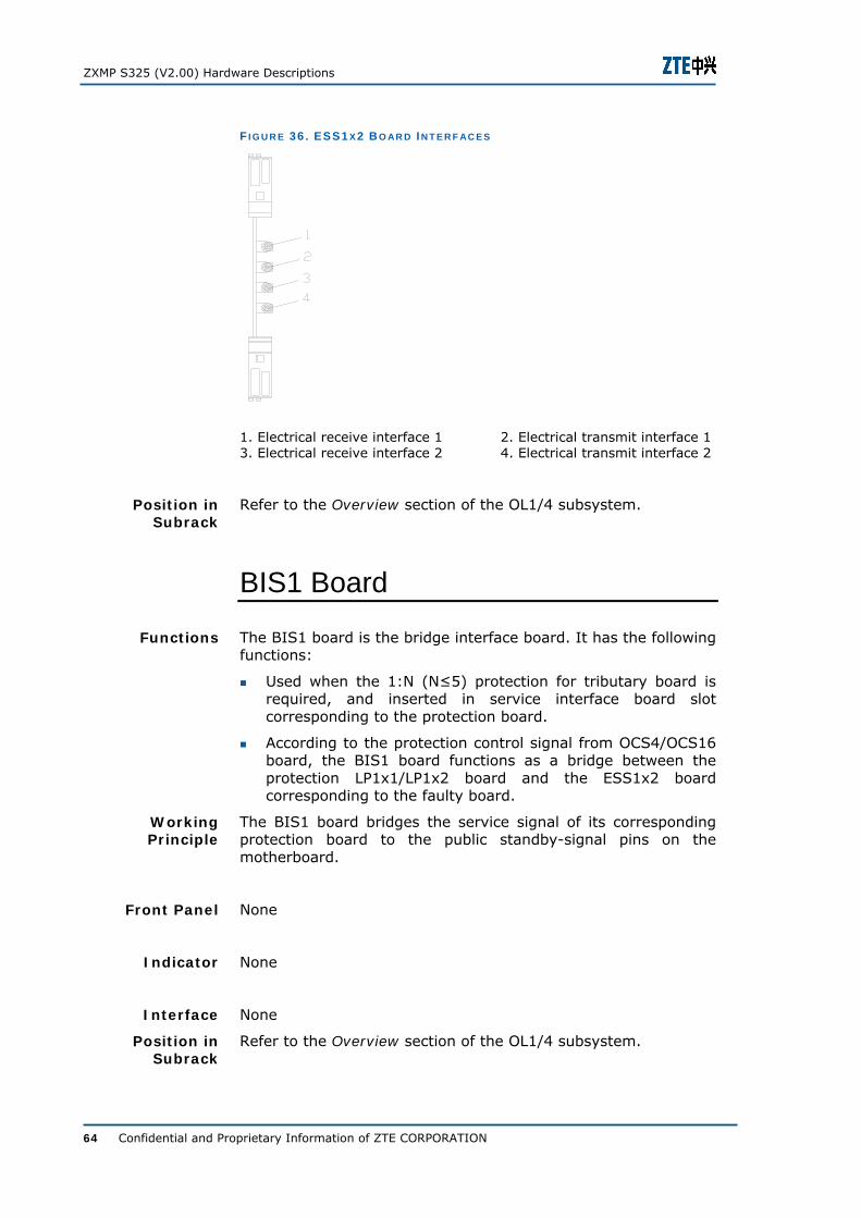
ZXMP S325 (V2.00) Hardware Descriptions
64 Confidential and Proprietary Information of ZTE CORPORATION
F I G U R E 36 . ESS1 X 2 B O AR D I N T E R F AC E S
1. Electrical receive interface 1 2. Electrical transmit interface 1 3. Electrical receive interface 2 4. Electrical transmit interface 2
Refer to the Overview section of the OL1/4 subsystem.
BIS1 Board
The BIS1 board is the bridge interface board. It has the following functions:
Used when the 1:N (N≤5) protection for tributary board is required, and inserted in service interface board slot corresponding to the protection board.
According to the protection control signal from OCS4/OCS16 board, the BIS1 board functions as a bridge between the protection LP1x1/LP1x2 board and the ESS1x2 board corresponding to the faulty board.
The BIS1 board bridges the service signal of its corresponding protection board to the public standby-signal pins on the motherboard.
None
None
None
Refer to the Overview section of the OL1/4 subsystem.
Position in Subrack
Functions
Working Principle
Front Panel
Indicator
Interface
Position in Subrack
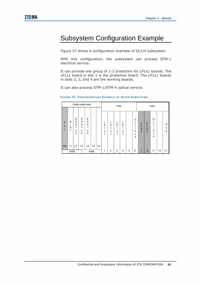
Chapter 3 - Boards
Confidential and Proprietary Information of ZTE CORPORATION 65
Subsystem Configuration Example
Figure 37 shows a configuration example of OL1/4 subsystem.
With this configuration, the subsystem can process STM-1 electrical service.
It can provide one group of 1:3 protection for LP1x1 boards. The LP1x1 board in slot 1 is the protection board. The LP1x1 boards in slots 2, 3, and 4 are the working boards.
It can also process STM-1/STM-4 optical service.
F I G U R E 37 . CO N F I G U R AT I O N E X AM P L E O F OL1/4 S U B S Y S T E M
Cable outlet area
PWR 12 177 865432 111
FANFAN
L6L5L4L3L2L1SAI
N
C
P
S
A
I
OCS4
OCS4
PWR
BIS1
ESS1x2
ESS1x2
ESS1x2
LP1x1
LP1x1
LP1x1
LP1x1
OL1/4x4
OL1/4x4
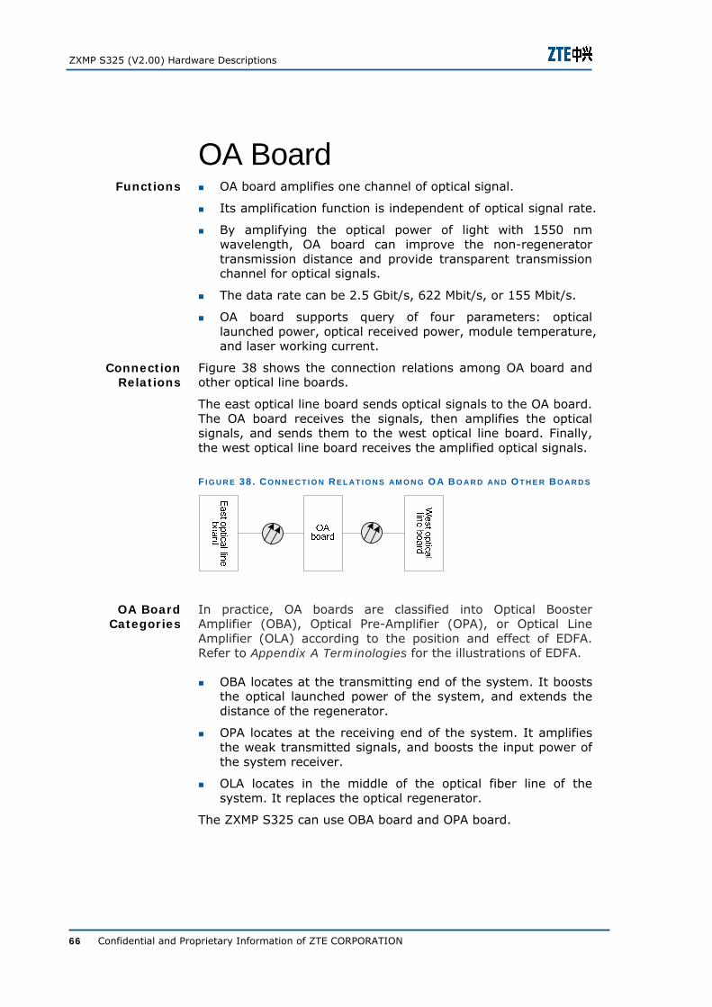
ZXMP S325 (V2.00) Hardware Descriptions
66 Confidential and Proprietary Information of ZTE CORPORATION
OA Board OA board amplifies one channel of optical signal.
Its amplification function is independent of optical signal rate.
By amplifying the optical power of light with 1550 nm wavelength, OA board can improve the non-regenerator transmission distance and provide transparent transmission channel for optical signals.
The data rate can be 2.5 Gbit/s, 622 Mbit/s, or 155 Mbit/s.
OA board supports query of four parameters: optical launched power, optical received power, module temperature, and laser working current.
Figure 38 shows the connection relations among OA board and other optical line boards.
The east optical line board sends optical signals to the OA board. The OA board receives the signals, then amplifies the optical signals, and sends them to the west optical line board. Finally, the west optical line board receives the amplified optical signals.
F I G U R E 38 . CO N N E C T I O N RE L AT I O N S AM O N G O A B O A R D AN D OT H E R B O AR D S
In practice, OA boards are classified into Optical Booster Amplifier (OBA), Optical Pre-Amplifier (OPA), or Optical Line Amplifier (OLA) according to the position and effect of EDFA. Refer to Appendix A Terminologies for the illustrations of EDFA.
OBA locates at the transmitting end of the system. It boosts the optical launched power of the system, and extends the distance of the regenerator.
OPA locates at the receiving end of the system. It amplifies the weak transmitted signals, and boosts the input power of the system receiver.
OLA locates in the middle of the optical fiber line of the system. It replaces the optical regenerator.
The ZXMP S325 can use OBA board and OPA board.
Functions
Connection Relations
OA Board Categories
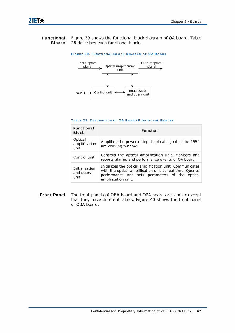
Chapter 3 - Boards
Confidential and Proprietary Information of ZTE CORPORATION 67
Figure 39 shows the functional block diagram of OA board. Table 28 describes each functional block.
F I G U R E 39 . FU N C T I O N AL B L O C K D I AG R A M O F O A B O A R D
Control unit
Optical amplificationunit
Initializationand query unit
Input opticalsignal
Output opticalsignal
NCP
T AB L E 28 . D E S C R I P T I O N O F O A B O AR D FU N C T I O N AL B L O C K S
Functional Block
Function
Optical amplification unit
Amplifies the power of input optical signal at the 1550 nm working window.
Control unit Controls the optical amplification unit. Monitors and reports alarms and performance events of OA board.
Initialization and query unit
Initializes the optical amplification unit. Communicates with the optical amplification unit at real time. Queries performance and sets parameters of the optical amplification unit.
The front panels of OBA board and OPA board are similar except that they have different labels. Figure 40 shows the front panel of OBA board.
Functional Blocks
Front Panel
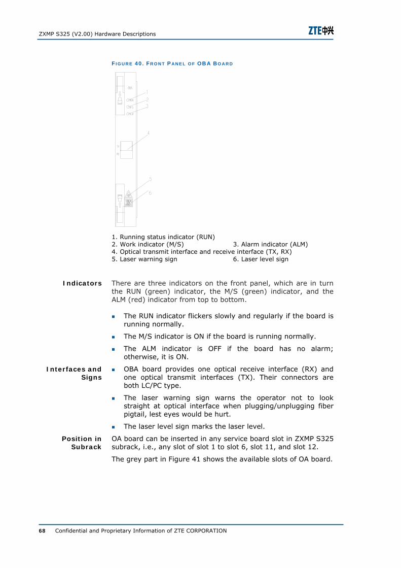
ZXMP S325 (V2.00) Hardware Descriptions
68 Confidential and Proprietary Information of ZTE CORPORATION
F I G U R E 40 . FR O N T P AN E L O F OB A B O A R D
1. Running status indicator (RUN) 2. Work indicator (M/S) 3. Alarm indicator (ALM) 4. Optical transmit interface and receive interface (TX, RX) 5. Laser warning sign 6. Laser level sign
There are three indicators on the front panel, which are in turn the RUN (green) indicator, the M/S (green) indicator, and the ALM (red) indicator from top to bottom.
The RUN indicator flickers slowly and regularly if the board is running normally.
The M/S indicator is ON if the board is running normally.
The ALM indicator is OFF if the board has no alarm; otherwise, it is ON.
OBA board provides one optical receive interface (RX) and one optical transmit interfaces (TX). Their connectors are both LC/PC type.
The laser warning sign warns the operator not to look straight at optical interface when plugging/unplugging fiber pigtail, lest eyes would be hurt.
The laser level sign marks the laser level.
OA board can be inserted in any service board slot in ZXMP S325 subrack, i.e., any slot of slot 1 to slot 6, slot 11, and slot 12.
The grey part in Figure 41 shows the available slots of OA board.
Indicators
Interfaces and Signs
Position in Subrack
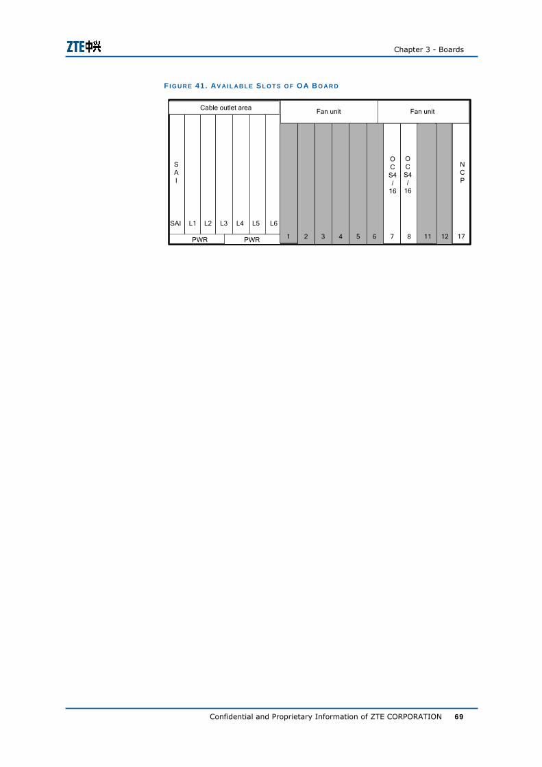
Chapter 3 - Boards
Confidential and Proprietary Information of ZTE CORPORATION 69
F I G U R E 41 . AV A I L A B L E S L O T S O F OA B O AR D
Cable outlet area
PWR PWR 12 177 865432 111
Fan unitFan unit
L6L5L4L3L2L1SAI
NCP
SAI
OCS4/
16
OCS4/
16
ZXMP S325 (V2.00) Hardware Descriptions
70 Confidential and Proprietary Information of ZTE CORPORATION
EP1 Subsystem Overview
Performs asynchronous mapping/demapping of PDH E1/T1 electrical signals.
Provides 1:N (N≤6) protection for tributary boards.
The EP1 subsystem comprises EPE1x21, EPT1x21, EPE1B, BIE1x21, and ESE1x21 boards.
Subsystem with different board combinations can implement different functions, as listed in Table 29.
T AB L E 29 . C O M B I N AT I O N S O F B O AR D S I N EP1 S U B S Y S T E M
Function Boards Involved
E1 electrical signal processing function
EPE1x21 (or EPE1B) and ESE1x21
1:N (N≤5) protection for E1 electrical tributary
EPE1x21 (or EPE1B), BIE1x21, and ESE1x21
1:6 protection for E1 electrical tributary
EPE1x21 (or EPE1B) [Note] and ESE1x21
T1 electrical signal processing function
EPT1x21 (or EPE1B) and ESE1x21
1:N (N≤5) protection for T1 electrical tributary
EPT1x21 (or EPE1B), BIE1x21, and ESE1x21
1:6 protection for T1 electrical tributary
EPT1x21 (or EPE1B) [Note] and ESE1x21
Note: The protection EPE1x21/EPT1x21/EPE1B board must be inserted in slot 11.
The positions of boards in EP1 subsystem are shown in Figure 42.
Subsystem Functions
Composition
Position in Subrack
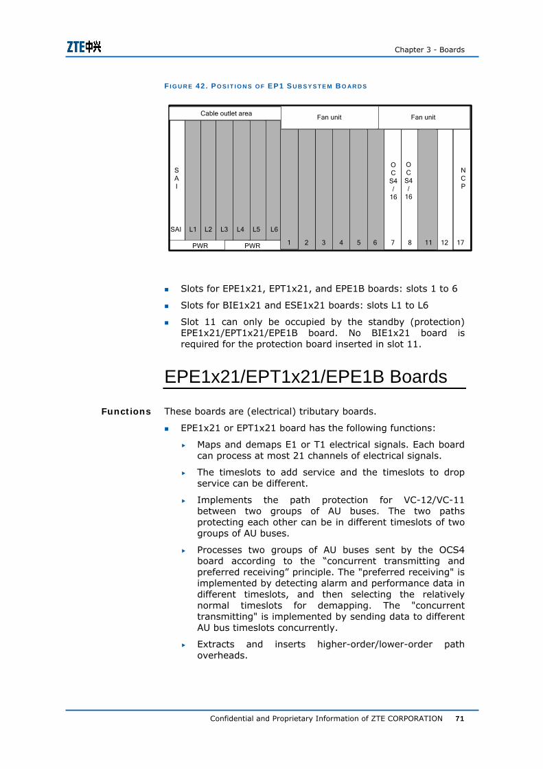
Chapter 3 - Boards
Confidential and Proprietary Information of ZTE CORPORATION 71
F I G U R E 42 . PO S I T I O N S O F EP1 S U B S Y S T E M BO AR D S
Cable outlet area
PWR PWR 12 177 865432 111
Fan unitFan unit
L6L5L4L3L2L1SAI
NCP
SAI
OCS4/
16
OCS4/
16
Slots for EPE1x21, EPT1x21, and EPE1B boards: slots 1 to 6
Slots for BIE1x21 and ESE1x21 boards: slots L1 to L6
Slot 11 can only be occupied by the standby (protection) EPE1x21/EPT1x21/EPE1B board. No BIE1x21 board is required for the protection board inserted in slot 11.
EPE1x21/EPT1x21/EPE1B Boards
These boards are (electrical) tributary boards.
EPE1x21 or EPT1x21 board has the following functions:
Maps and demaps E1 or T1 electrical signals. Each board can process at most 21 channels of electrical signals.
The timeslots to add service and the timeslots to drop service can be different.
Implements the path protection for VC-12/VC-11 between two groups of AU buses. The two paths protecting each other can be in different timeslots of two groups of AU buses.
Processes two groups of AU buses sent by the OCS4 board according to the “concurrent transmitting and preferred receiving” principle. The "preferred receiving" is implemented by detecting alarm and performance data in different timeslots, and then selecting the relatively normal timeslots for demapping. The "concurrent transmitting" is implemented by sending data to different AU bus timeslots concurrently.
Extracts and inserts higher-order/lower-order path overheads.
Functions
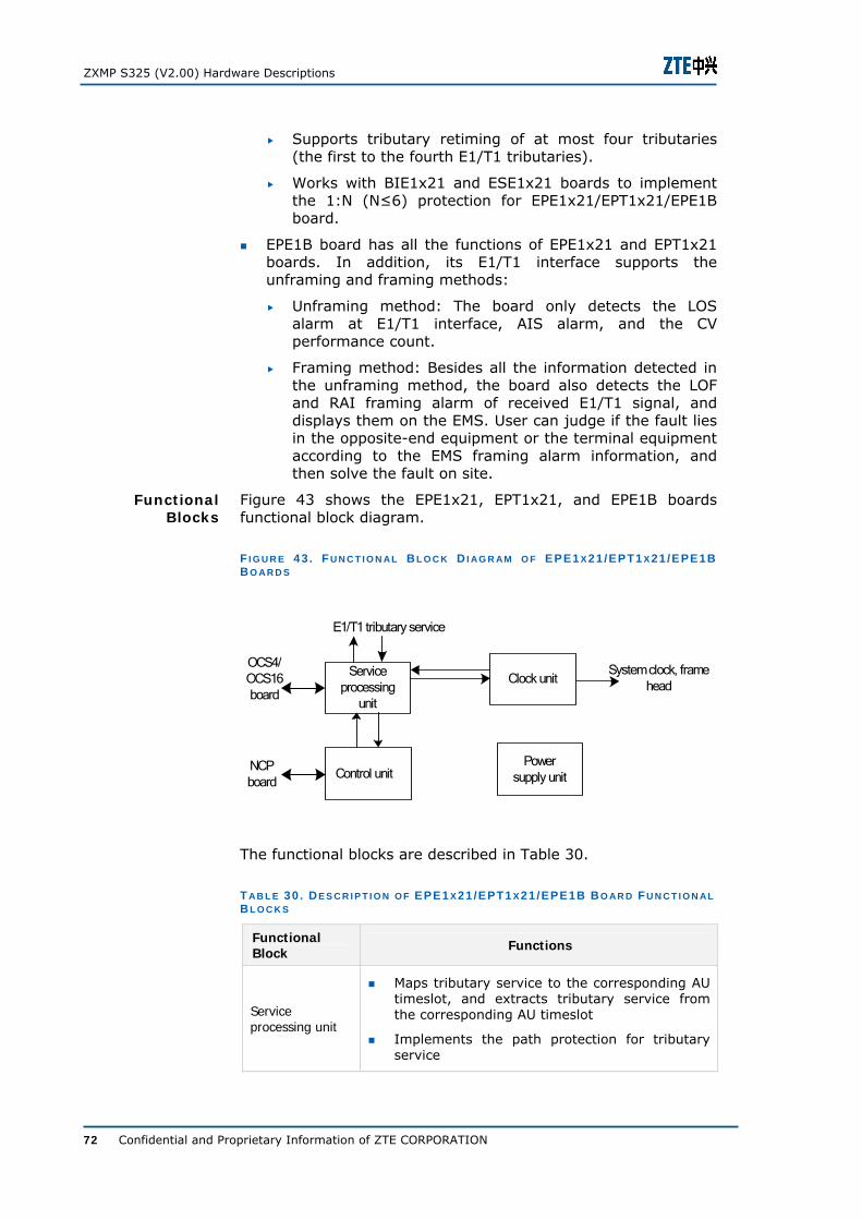
ZXMP S325 (V2.00) Hardware Descriptions
72 Confidential and Proprietary Information of ZTE CORPORATION
Supports tributary retiming of at most four tributaries (the first to the fourth E1/T1 tributaries).
Works with BIE1x21 and ESE1x21 boards to implement the 1:N (N≤6) protection for EPE1x21/EPT1x21/EPE1B board.
EPE1B board has all the functions of EPE1x21 and EPT1x21 boards. In addition, its E1/T1 interface supports the unframing and framing methods:
Unframing method: The board only detects the LOS alarm at E1/T1 interface, AIS alarm, and the CV performance count.
Framing method: Besides all the information detected in the unframing method, the board also detects the LOF and RAI framing alarm of received E1/T1 signal, and displays them on the EMS. User can judge if the fault lies in the opposite-end equipment or the terminal equipment according to the EMS framing alarm information, and then solve the fault on site.
Figure 43 shows the EPE1x21, EPT1x21, and EPE1B boards functional block diagram.
F I G U R E 43 . FU N C T I O N AL B L O C K D I AG R AM O F EPE1 X 21 /EPT1 X 21 /EPE1B B O AR D S
Service processing
unit
Clock unit
E1/T1 tributary service
System clock, frame head
Control unit Power
supply unitNCP board
OCS4/OCS16 board
The functional blocks are described in Table 30.
T AB L E 30 . D E S C R I P T I O N O F EPE1 X21 /EPT1 X 21 /EPE1B B O AR D FU N C T I O N AL B L O C K S
Functional Block Functions
Service processing unit
Maps tributary service to the corresponding AU timeslot, and extracts tributary service from the corresponding AU timeslot
Implements the path protection for tributary service
Functional Blocks
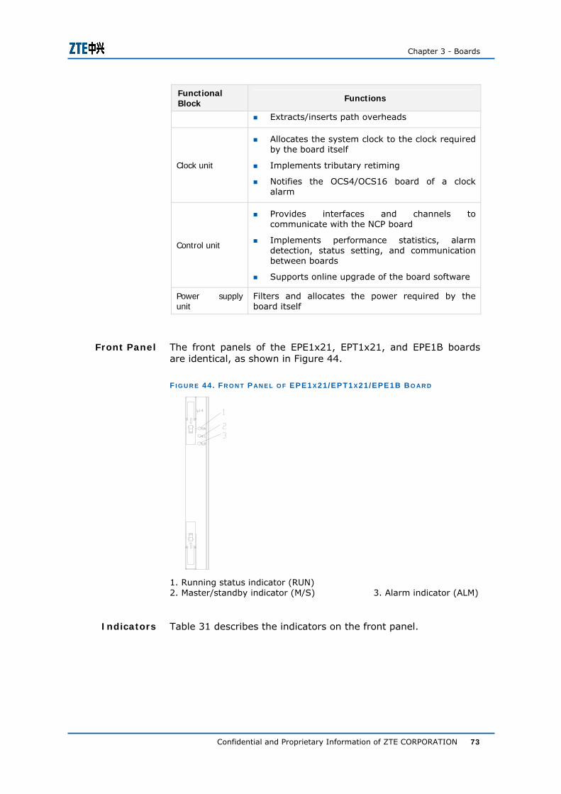
Chapter 3 - Boards
Confidential and Proprietary Information of ZTE CORPORATION 73
Functional Block Functions
Extracts/inserts path overheads
Clock unit
Allocates the system clock to the clock required by the board itself
Implements tributary retiming
Notifies the OCS4/OCS16 board of a clock alarm
Control unit
Provides interfaces and channels to communicate with the NCP board
Implements performance statistics, alarm detection, status setting, and communication between boards
Supports online upgrade of the board software
Power supply unit
Filters and allocates the power required by the board itself
The front panels of the EPE1x21, EPT1x21, and EPE1B boards are identical, as shown in Figure 44.
F I G U R E 44 . FR O N T P AN E L O F EPE1 X 21/EPT1 X 21/EPE1B B O AR D
1. Running status indicator (RUN) 2. Master/standby indicator (M/S) 3. Alarm indicator (ALM)
Table 31 describes the indicators on the front panel.
Front Panel
Indicators
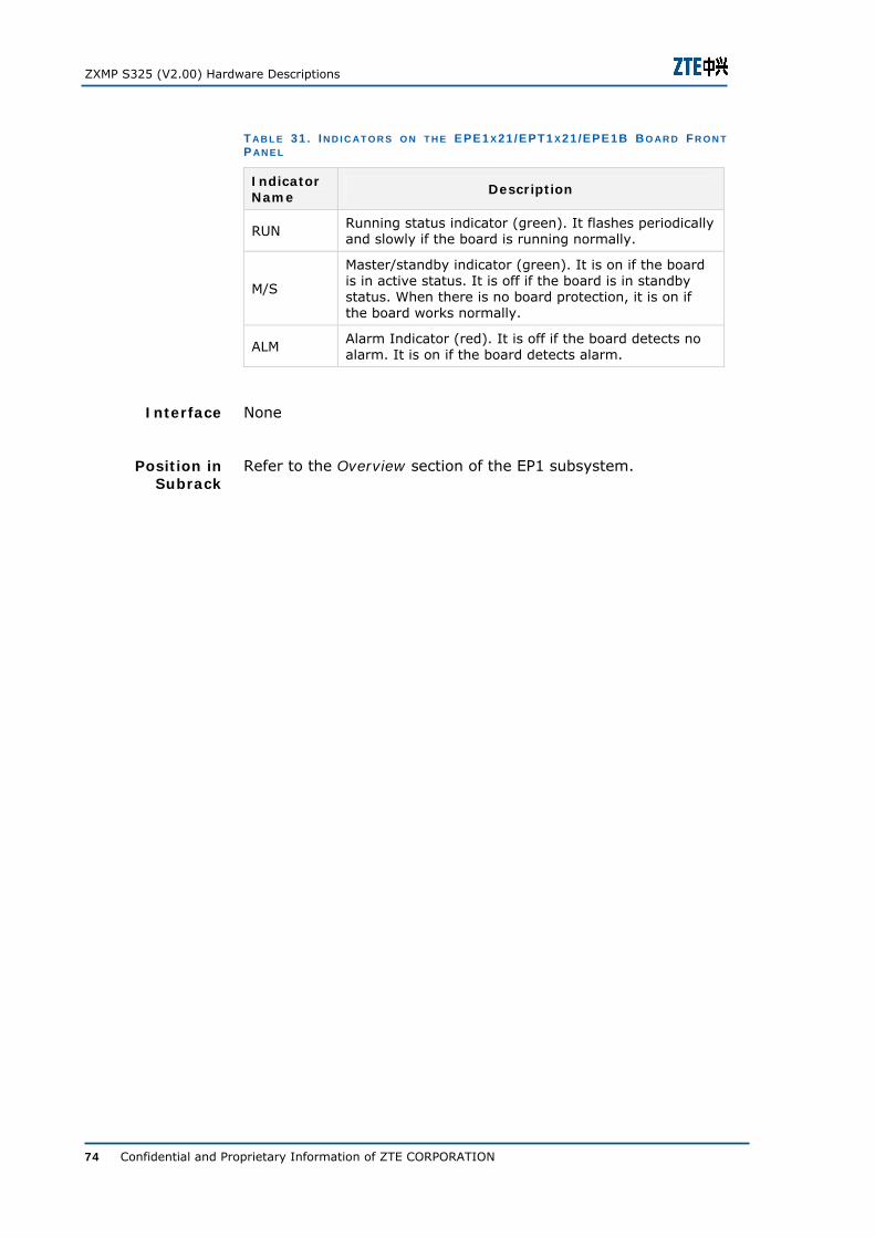
ZXMP S325 (V2.00) Hardware Descriptions
74 Confidential and Proprietary Information of ZTE CORPORATION
T AB L E 31 . I N D I C AT O R S O N T H E EPE1 X 21 /EPT1 X21 /EPE1B B O AR D FR O N T P AN E L
Indicator Name
Description
RUN Running status indicator (green). It flashes periodically and slowly if the board is running normally.
M/S
Master/standby indicator (green). It is on if the board is in active status. It is off if the board is in standby status. When there is no board protection, it is on if the board works normally.
ALM Alarm Indicator (red). It is off if the board detects no alarm. It is on if the board detects alarm.
None
Refer to the Overview section of the EP1 subsystem.
Interface
Position in Subrack
Chapter 3 - Boards
Confidential and Proprietary Information of ZTE CORPORATION 75
ESE1x21 Board
The ESE1x21 board is the interface switching board. It has the following functions:
Provides twenty-one E1/T1 electrical interface pairs for EPE1x21/EPT1x21/EPE1B board.
When the protection for tributary board is not required, ESE1x21 board only performs E1/T1 electrical interface function.
When the 1:N (N≤5) protection for tributary board is required, ESE1x21 board works with the BIE1x21 board to implement the 1:N (N≤5) protection for tributary board.
When the 1:6 protection for tributary board is required, ESE1x21 board works with the protection tributary board inserted in slot 11 to implement the 1:6 protection.
At the receive side, the ESE1x21 board receives the electrical signal from the outside, and then sends the signal to the electrical tributary board via the motherboard for processing.
At the transmit side, the ESE1x21 board receives the signal sent by the electrical tributary board via the motherboard, and then sends the signal to the outside.
In the case of 1:N (N≤6) protection for tributary board, ESE1x21 board determines whether to send the electrical signal to the working tributary board or to the protection tributary board according to the control signal from OCS4/OCS16 board.
None
None
Figure 45 illustrates the ESE1x21 board interface.
Functions
Working Principle
Front Panel
Indicator
Interface
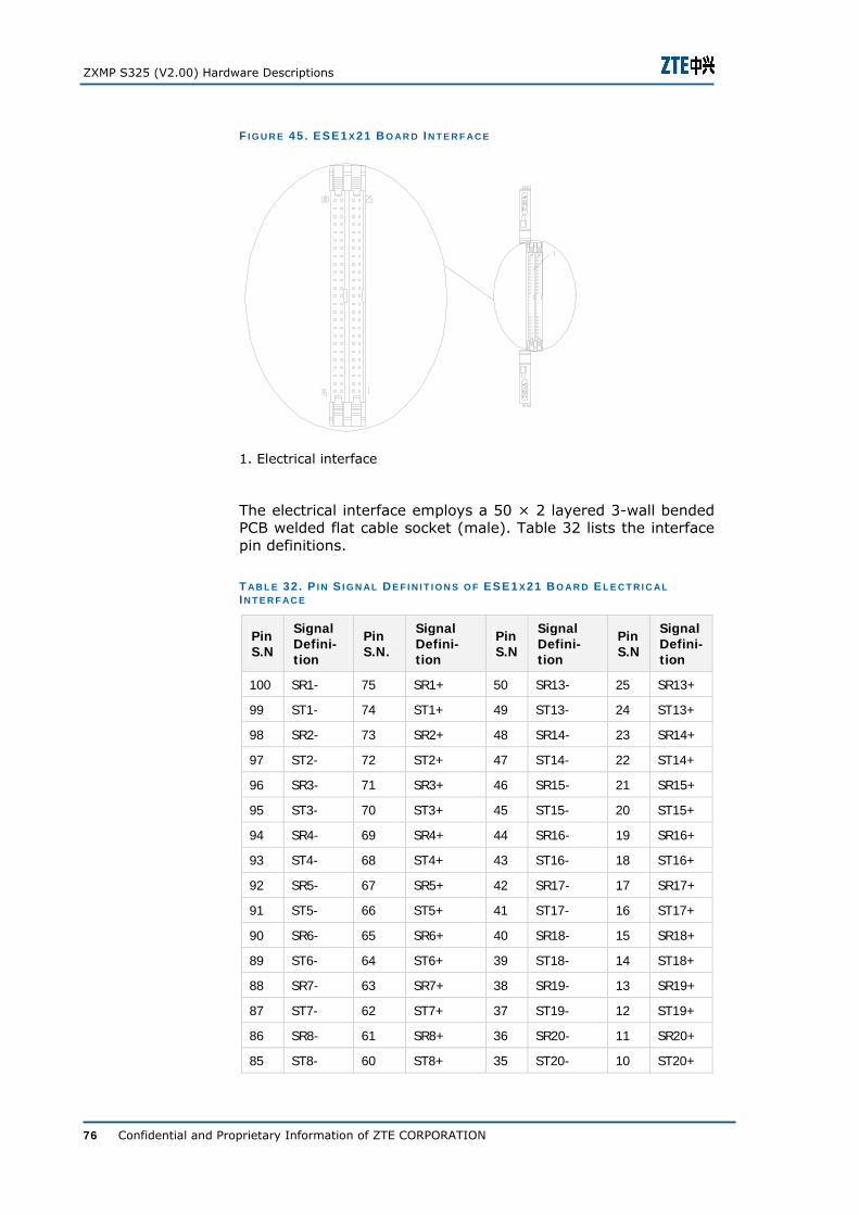
ZXMP S325 (V2.00) Hardware Descriptions
76 Confidential and Proprietary Information of ZTE CORPORATION
F I G U R E 45 . ESE1 X 21 B O AR D I N T E R F AC E
1. Electrical interface
The electrical interface employs a 50 × 2 layered 3-wall bended PCB welded flat cable socket (male). Table 32 lists the interface pin definitions.
T AB L E 32 . P I N S I G N AL D E F I N I T I O N S O F ESE1 X 21 B O AR D E L E C T R I C AL I N T E R F AC E
Pin S.N
Signal Defini-tion
Pin S.N.
Signal Defini-tion
Pin S.N
Signal Defini-tion
Pin S.N
Signal Defini-tion
100 SR1- 75 SR1+ 50 SR13- 25 SR13+
99 ST1- 74 ST1+ 49 ST13- 24 ST13+
98 SR2- 73 SR2+ 48 SR14- 23 SR14+
97 ST2- 72 ST2+ 47 ST14- 22 ST14+
96 SR3- 71 SR3+ 46 SR15- 21 SR15+
95 ST3- 70 ST3+ 45 ST15- 20 ST15+
94 SR4- 69 SR4+ 44 SR16- 19 SR16+
93 ST4- 68 ST4+ 43 ST16- 18 ST16+
92 SR5- 67 SR5+ 42 SR17- 17 SR17+
91 ST5- 66 ST5+ 41 ST17- 16 ST17+
90 SR6- 65 SR6+ 40 SR18- 15 SR18+
89 ST6- 64 ST6+ 39 ST18- 14 ST18+
88 SR7- 63 SR7+ 38 SR19- 13 SR19+
87 ST7- 62 ST7+ 37 ST19- 12 ST19+
86 SR8- 61 SR8+ 36 SR20- 11 SR20+
85 ST8- 60 ST8+ 35 ST20- 10 ST20+
Chapter 3 - Boards
Confidential and Proprietary Information of ZTE CORPORATION 77
Pin S.N
Signal Defini-tion
Pin S.N.
Signal Defini-tion
Pin S.N
Signal Defini-tion
Pin S.N
Signal Defini-tion
84 SR9- 59 SR9+ 34 SR21- 9 SR21+
83 ST9- 58 ST9+ 33 ST21- 8 ST21+
82 SR10- 57 SR10+ 32 - 7 -
81 ST10- 56 ST10+ 31 - 6 -
80 SR11- 55 SR11+ 30 - 5 -
79 ST11- 54 ST11+ 29 - 4 -
78 SR12- 53 SR12+ 28 - 3 -
77 ST12- 52 ST12+ 27 - 2 -
76 - 51 - 26 - 1 -
Notes:
Refer to Figure 45 for the pin numberings.
SRn- and SRn+ represent for the received signal of channel n, while STn- and STn+ represent for the transmitted signal of channel n.
Refer to the Overview section of the EP1 subsystem.
BIE1x21 Board
The BIEx21 board is the bridge interface board. It has the following functions:
Functions as a bridge between the protection tributary board and the interface switching board corresponding to the faulty tributary board.
Used only when 1:N (N≤5) protection for E1/T1 tributary board is required.
Inserted in the interface board slot corresponding to the protection EPE1x21/EPT1x21/EPE1B board.
The BIE1x21 board bridges the service signal of its corresponding protection board to the public standby-signal pins on the motherboard.
None
None
Position in Subrack
Functions
Working Principle
Front Panel
Indicator
ZXMP S325 (V2.00) Hardware Descriptions
78 Confidential and Proprietary Information of ZTE CORPORATION
None
Refer to the Overview section of the EP1 subsystem.
Note: If the EPE1x21/EPT1x21/EPE1B protection board is inserted in slot 11, BIE1x21 board is not needed.
Subsystem Configuration Example
Figure 46 shows a configuration example of EP1 subsystem.
With this configuration, the system can process E1 electrical service.
It can provide one group of 1:3 protection for EPE1x21 boards. The EPE1x21 board in slot 1 is the protection board. The EPE1x21 boards in slots 2, 3, 4 are the working boards.
It can also process STM-1/STM-4 optical service.
F I G U R E 46 . CO N F I G U R AT I O N E X AM P L E O F EP1 S U B S Y S T E M
Cable outlet area
PWR 12 177 865432 111
FANFAN
L6L5L4L3L2L1SAI
NCP
SAI
OCS4
OCS4
PWR
BIE1x
21
ESE1x
21
ESE1x
21
ESE1x
21
EPE1x
21
OL1/4x4
OL1/4x4
EPE1x
21
EPE1x
21
EPE1x
21
Interface
Position in Subrack
Chapter 3 - Boards
Confidential and Proprietary Information of ZTE CORPORATION 79
EP3 Subsystem Overview
Performs the asynchronous mapping/demapping of PDH E3/T3 electrical signals.
Provides 1:N (N≤5) protection for tributary boards.
Comprises EP3x3, ESE3x3, and BIE3x3 boards.
Can implement different functions with different board combinations, as listed in Table 33.
T AB L E 33 . C O M B I N AT I O N O F B O AR D S I N EP3 S U B S Y S T E M
Function Boards Involved
E3 electrical signal processing function EP3x3, ESE3x3
1:N (N≤5) protection for E3 electrical tributary EP3x3, BIE3x3, ESE3x3
T3 electrical signal processing function EP3x3, ESE3x3
1:N (N≤5) protection for T3 electrical tributary EP3x3, BIE3x3, ESE3x3
Figure 47 shows the positions of boards in the EP3 subsystem.
F I G U R E 47 . EP3 S U B S Y S T E M B O AR D P O S I T I O N S
Cable outlet area
PWR PWR 12 177 865432 111
Fan unitFan unit
L6L5L4L3L2L1SAI
NCP
SAI
OCS4/
16
OCS4/
16
Slots for EP3x3 boards:
No board protection: slots 1 to 6
Subsystem Functions
Composition
Position in Subrack
ZXMP S325 (V2.00) Hardware Descriptions
80 Confidential and Proprietary Information of ZTE CORPORATION
With 1:N (N≤5) board protection: the EP3x3 protection board must be inserted in slot 1.
Slots for ESE3x3 board: slots L1 to L6
Slot for BIE3x3 board: slot L1
EP3x3 Board
EP3x3 board is a tributary board. Its functions are described below:
Processes three channels of E3 or T3 services. Its port rate can be configured as E3 or T3 via the EMS.
Supports the mapping/demapping and multiplexing/ demultiplexing of three channels of E3 or T3 signals into/from any timeslot of AU-4.
Supports the unframing and framing methods:
Unframing method: For E3 interface, EP3x3 board detects LOS/AIS alarm and CV performance count. For T3 interface, EP3x3 board only detects LOS alarm and CV performance count.
Framing method: Besides all the information detected in the unframing method, EP3x3 board also detects the LOF/RAI framing alarm of received E3/T3 signal, and AIS alarm of received T3 signal; and displays them on the EMS. User can judge whether fault is caused by transmission equipment or by terminal equipment according to the EMS framing alarm information, and then solve the fault on site.
The timeslots to add service and the timeslots to drop service can be different.
Implements the path protection for VC-3 between two groups of AU buses.
Supports the extraction and insertion of VC-3 path overhead.
Reads the alarm and performance information of the AU bus, the E3/T3 interface, and the VC-3 path. And reports them to the EMS.
Can work with BIE3x3 and ESE3x3 boards to implement the 1:N (N≤5) protection for EP3x3 board.
Figure 48 shows the functional blocks of EP3x3 board.
Functions
Functional Blocks
Chapter 3 - Boards
Confidential and Proprietary Information of ZTE CORPORATION 81
F I G U R E 48 . FU N C T I O N AL B L O C K D I AG R A M O F EP3 X 3 B O AR D
Service processing unit
Control unit
Clock unit
Line interface unit E3/T3 tributary service
System clock
Reference clock
NCP board
OCS4/OCS16 board
Table 34 describes the functional blocks.
T AB L E 34 . FU N C T I O N AL B L O C K S O F EP3X 3 B O AR D
Functional Block Functions
Clock unit Allocates the system clock to the clock required by
the board itself.
Provides clock source to the line interface unit.
Line interface unit Outputs/inputs the E3 or T3 signal.
Service processing unit
Maps and demaps the service timeslots of the board.
Implements the path protection for tributary service.
Processes pointer and path overhead.
Control unit
Provides channels to communicate with the NCP board.
Implements performance statistics, alarm detection, status setting, and communication between boards.
The front panels of EP3x3 board is shown in Figure 49. Front Panel
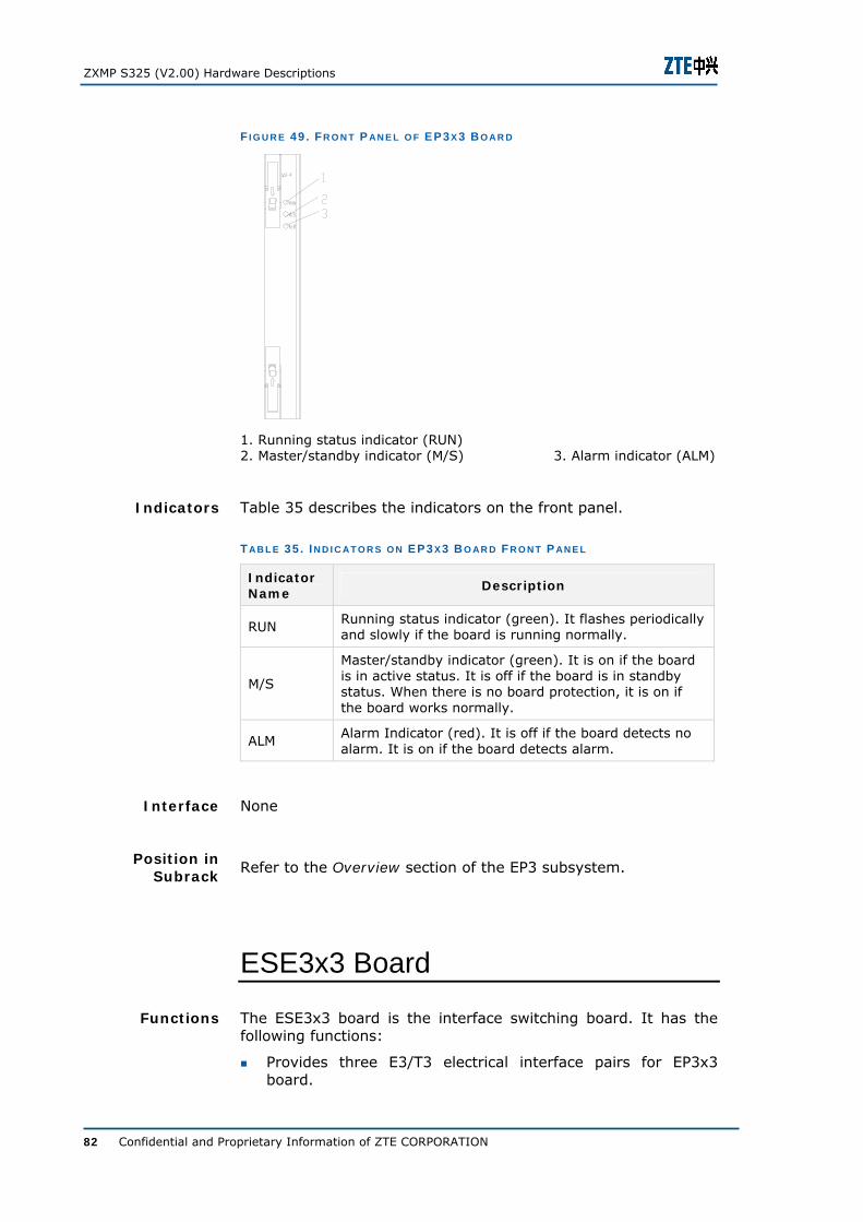
ZXMP S325 (V2.00) Hardware Descriptions
82 Confidential and Proprietary Information of ZTE CORPORATION
F I G U R E 49 . FR O N T P AN E L O F EP3X 3 B O A R D
1. Running status indicator (RUN) 2. Master/standby indicator (M/S) 3. Alarm indicator (ALM)
Table 35 describes the indicators on the front panel.
T AB L E 35 . I N D I C AT O R S O N EP3 X 3 B O AR D FR O N T P AN E L
Indicator Name
Description
RUN Running status indicator (green). It flashes periodically and slowly if the board is running normally.
M/S
Master/standby indicator (green). It is on if the board is in active status. It is off if the board is in standby status. When there is no board protection, it is on if the board works normally.
ALM Alarm Indicator (red). It is off if the board detects no alarm. It is on if the board detects alarm.
None
Refer to the Overview section of the EP3 subsystem.
ESE3x3 Board
The ESE3x3 board is the interface switching board. It has the following functions:
Provides three E3/T3 electrical interface pairs for EP3x3 board.
Indicators
Interface
Position in Subrack
Functions
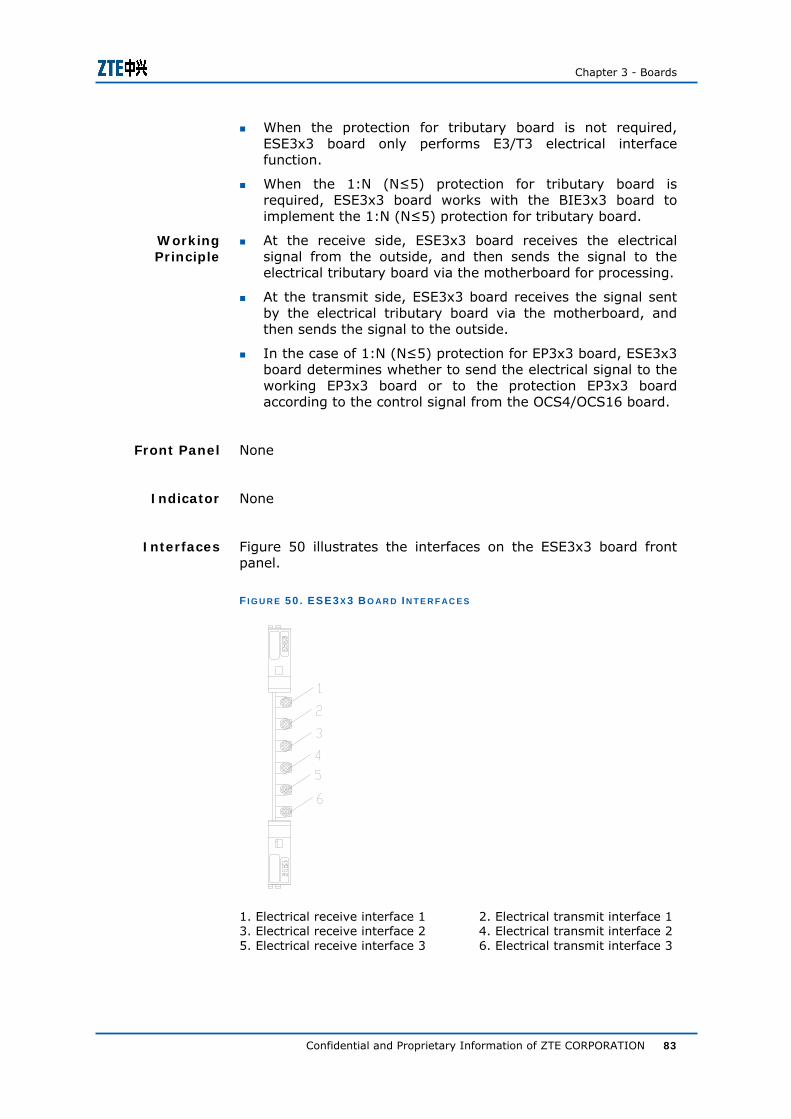
Chapter 3 - Boards
Confidential and Proprietary Information of ZTE CORPORATION 83
When the protection for tributary board is not required, ESE3x3 board only performs E3/T3 electrical interface function.
When the 1:N (N≤5) protection for tributary board is required, ESE3x3 board works with the BIE3x3 board to implement the 1:N (N≤5) protection for tributary board.
At the receive side, ESE3x3 board receives the electrical signal from the outside, and then sends the signal to the electrical tributary board via the motherboard for processing.
At the transmit side, ESE3x3 board receives the signal sent by the electrical tributary board via the motherboard, and then sends the signal to the outside.
In the case of 1:N (N≤5) protection for EP3x3 board, ESE3x3 board determines whether to send the electrical signal to the working EP3x3 board or to the protection EP3x3 board according to the control signal from the OCS4/OCS16 board.
None
None
Figure 50 illustrates the interfaces on the ESE3x3 board front panel.
F I G U R E 50 . ESE3 X 3 B O AR D I N T E R F AC E S
1. Electrical receive interface 1 2. Electrical transmit interface 1 3. Electrical receive interface 2 4. Electrical transmit interface 2 5. Electrical receive interface 3 6. Electrical transmit interface 3
Working Principle
Front Panel
Indicator
Interfaces
ZXMP S325 (V2.00) Hardware Descriptions
84 Confidential and Proprietary Information of ZTE CORPORATION
ESE3x3 board provides three electrical interface pairs which employ 1.0/2.3 bended PCB welded (screws attached) sockets (female).
Refer to the Overview section of the EP3 subsystem.
BIE3x3 Board
The BIE3x3 board is the bridge interface board. It has the following functions:
Functions as a bridge between the protection tributary board and the interface switching board corresponding to the faulty tributary board.
Used only when 1:N (N≤5) protection for EP3x3 board is required.
Inserted in the service interface board slot corresponding to the protection EP3x3 board.
The BIE3x3 board bridges the service signal of its corresponding protection board to the public standby-signal pins on the motherboard.
None
None
None
Refer to the Overview section of the EP3 subsystem.
Subsystem Configuration Example
Figure 51 shows a configuration example of EP3 subsystem.
With this configuration, the system can process E3 electrical service.
It can provide one group of 1:3 protection for EP3x3 boards. The EP3x3 board in slot 1 is the protection board. The EP3x3 boards in slots 2, 3, 4 are the working boards.
It can also process STM-1/STM-4 optical service.
Position in Subrack
Functions
Working Principle
Front Panel
Indicator
Interface
Position in Subrack
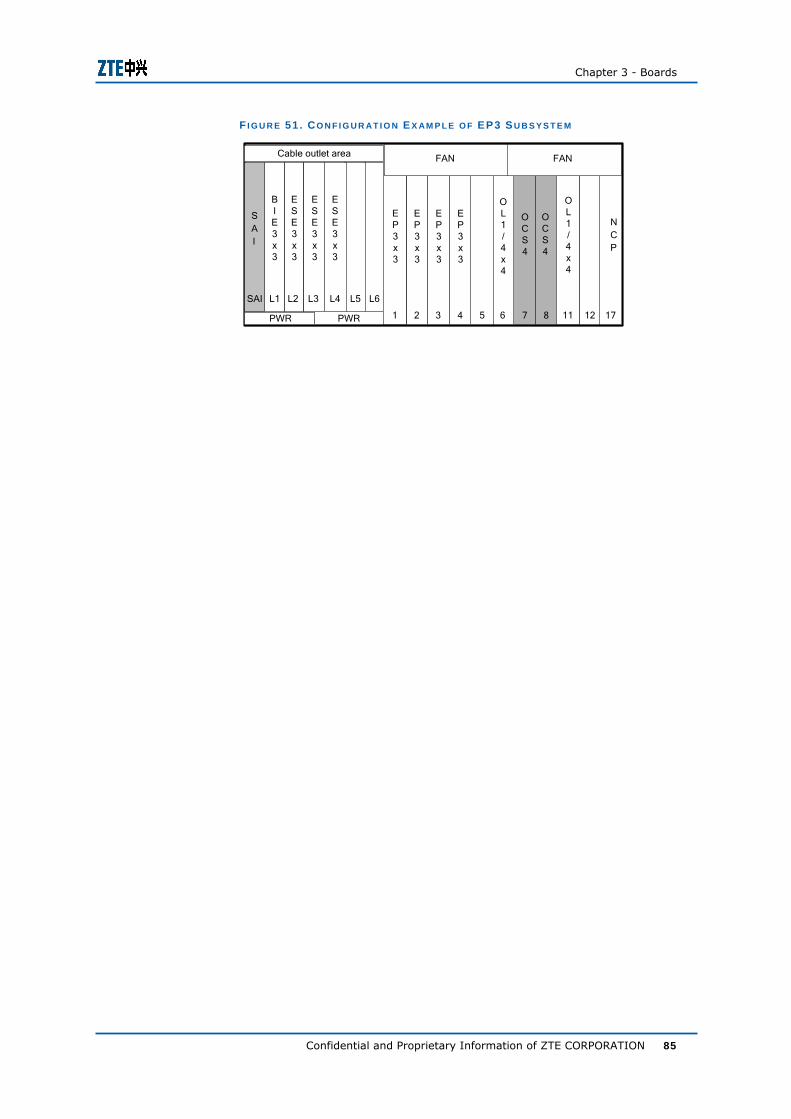
Chapter 3 - Boards
Confidential and Proprietary Information of ZTE CORPORATION 85
F I G U R E 51 . CO N F I G U R AT I O N E X AM P L E O F EP3 S U B S Y S T E M
Cable outlet area
PWR 12 177 865432 111
FANFAN
L6L5L4L3L2L1SAI
NCP
SAI
OCS4
OCS4
PWR
BIE3x3
ESE3x3
ESE3x3
ESE3x3
EP3x3
OL1/4x4
OL1/4x4
EP3x3
EP3x3
EP3x3
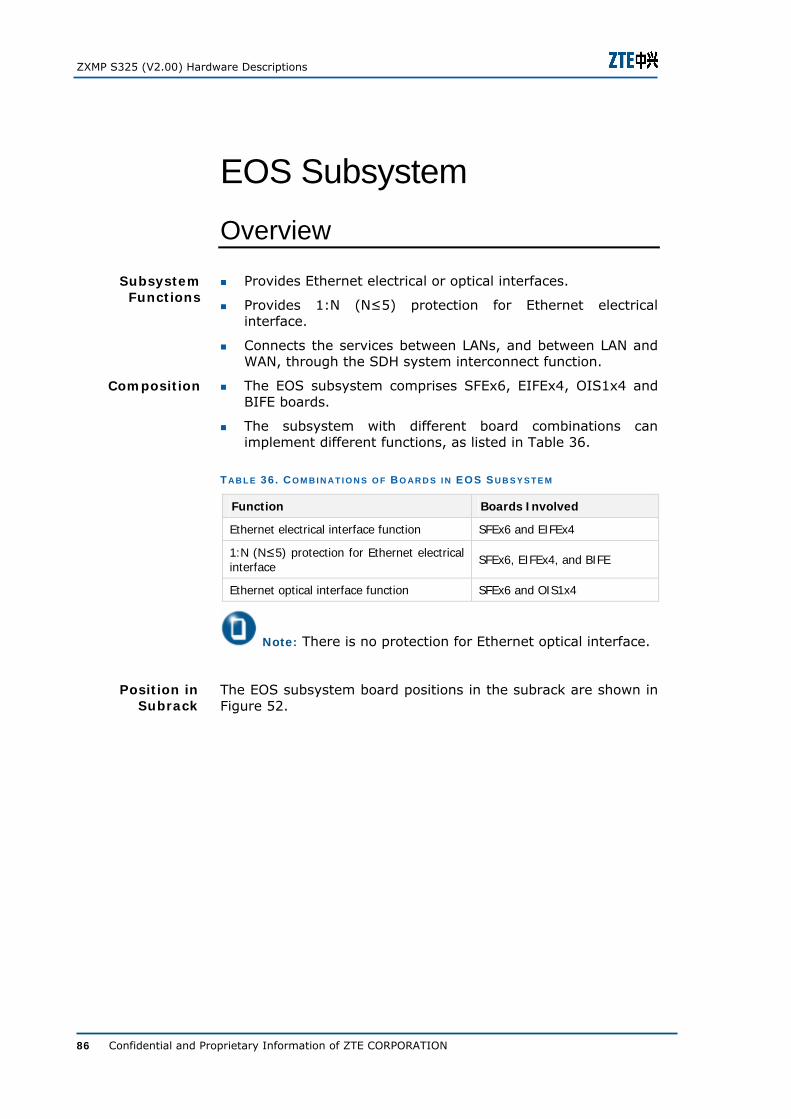
ZXMP S325 (V2.00) Hardware Descriptions
86 Confidential and Proprietary Information of ZTE CORPORATION
EOS Subsystem Overview
Provides Ethernet electrical or optical interfaces.
Provides 1:N (N≤5) protection for Ethernet electrical interface.
Connects the services between LANs, and between LAN and WAN, through the SDH system interconnect function.
The EOS subsystem comprises SFEx6, EIFEx4, OIS1x4 and BIFE boards.
The subsystem with different board combinations can implement different functions, as listed in Table 36.
T AB L E 36 . C O M B I N AT I O N S O F B O AR D S I N EOS S U B S Y S T E M
Function Boards Involved
Ethernet electrical interface function SFEx6 and EIFEx4
1:N (N≤5) protection for Ethernet electrical interface SFEx6, EIFEx4, and BIFE
Ethernet optical interface function SFEx6 and OIS1x4
Note: There is no protection for Ethernet optical interface.
The EOS subsystem board positions in the subrack are shown in Figure 52.
Subsystem Functions
Composition
Position in Subrack
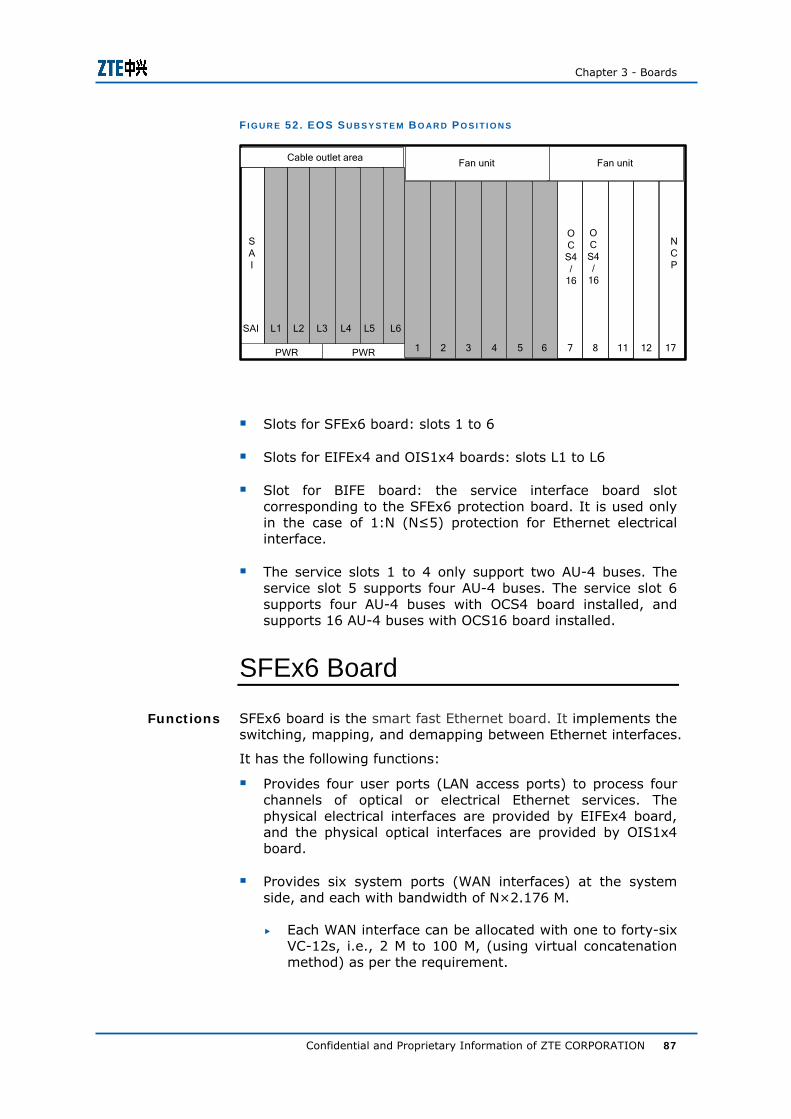
Chapter 3 - Boards
Confidential and Proprietary Information of ZTE CORPORATION 87
F I G U R E 52 . EOS S U B S Y S T E M B O AR D P O S I T I O N S
Cable outlet area
PWR PWR 12 177 865432 111
Fan unitFan unit
L6L5L4L3L2L1SAI
NCP
SAI
OCS4/
16
OCS4/
16
Slots for SFEx6 board: slots 1 to 6
Slots for EIFEx4 and OIS1x4 boards: slots L1 to L6
Slot for BIFE board: the service interface board slot corresponding to the SFEx6 protection board. It is used only in the case of 1:N (N≤5) protection for Ethernet electrical interface.
The service slots 1 to 4 only support two AU-4 buses. The service slot 5 supports four AU-4 buses. The service slot 6 supports four AU-4 buses with OCS4 board installed, and supports 16 AU-4 buses with OCS16 board installed.
SFEx6 Board
SFEx6 board is the smart fast Ethernet board. It implements the switching, mapping, and demapping between Ethernet interfaces.
It has the following functions:
Provides four user ports (LAN access ports) to process four channels of optical or electrical Ethernet services. The physical electrical interfaces are provided by EIFEx4 board, and the physical optical interfaces are provided by OIS1x4 board.
Provides six system ports (WAN interfaces) at the system side, and each with bandwidth of N×2.176 M.
Each WAN interface can be allocated with one to forty-six VC-12s, i.e., 2 M to 100 M, (using virtual concatenation method) as per the requirement.
Functions
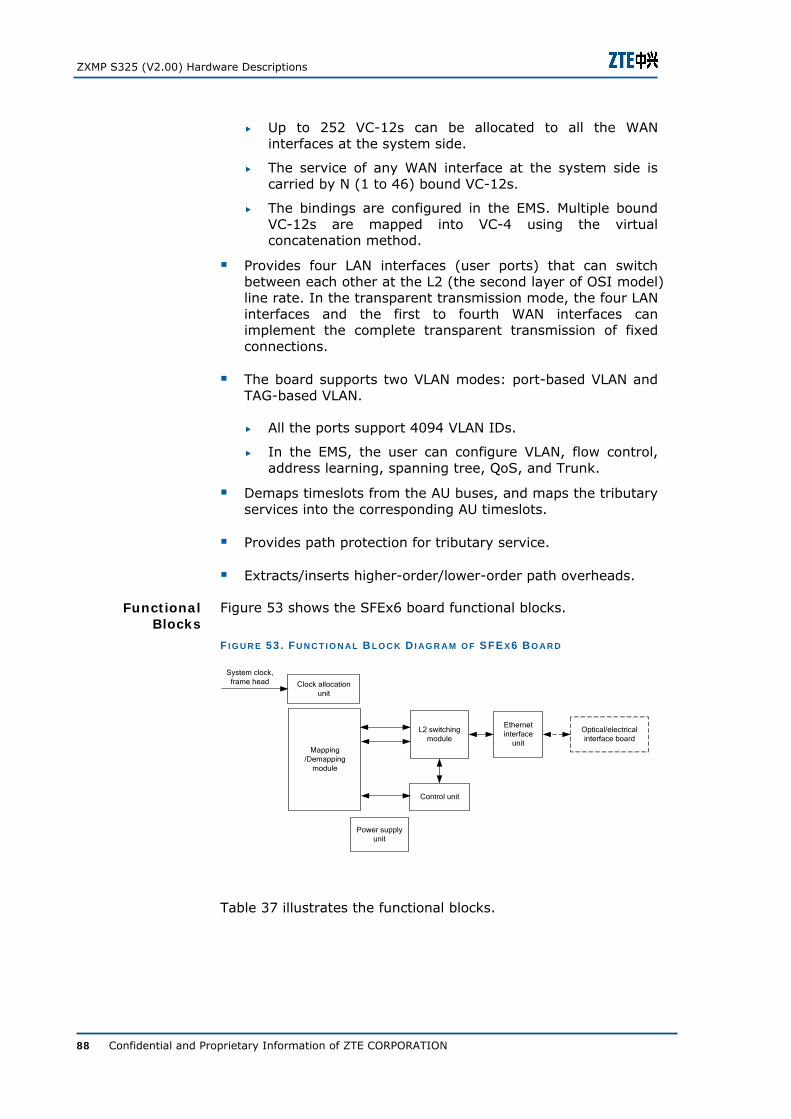
ZXMP S325 (V2.00) Hardware Descriptions
88 Confidential and Proprietary Information of ZTE CORPORATION
Up to 252 VC-12s can be allocated to all the WAN interfaces at the system side.
The service of any WAN interface at the system side is carried by N (1 to 46) bound VC-12s.
The bindings are configured in the EMS. Multiple bound VC-12s are mapped into VC-4 using the virtual concatenation method.
Provides four LAN interfaces (user ports) that can switch between each other at the L2 (the second layer of OSI model) line rate. In the transparent transmission mode, the four LAN interfaces and the first to fourth WAN interfaces can implement the complete transparent transmission of fixed connections.
The board supports two VLAN modes: port-based VLAN and TAG-based VLAN.
All the ports support 4094 VLAN IDs.
In the EMS, the user can configure VLAN, flow control, address learning, spanning tree, QoS, and Trunk.
Demaps timeslots from the AU buses, and maps the tributary services into the corresponding AU timeslots.
Provides path protection for tributary service.
Extracts/inserts higher-order/lower-order path overheads.
Figure 53 shows the SFEx6 board functional blocks.
F I G U R E 53 . FU N C T I O N AL B L O C K D I AG R A M O F SFE X 6 B O AR D
Mapping/Demapping
module
Control unit
Clock allocation unit
Power supply unit
System clock, frame head
L2 switching module
Ethernet interface
unit
Optical/electrical interface board
Table 37 illustrates the functional blocks.
Functional Blocks
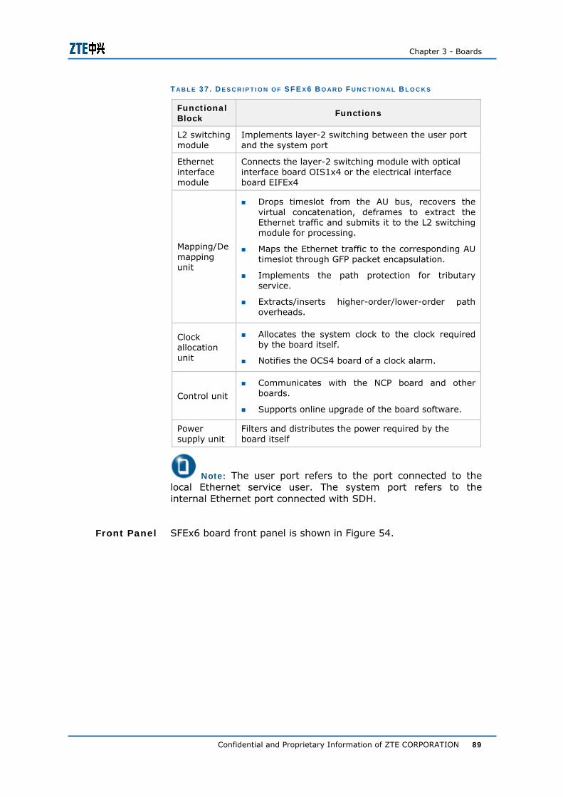
Chapter 3 - Boards
Confidential and Proprietary Information of ZTE CORPORATION 89
T AB L E 37 . D E S C R I P T I O N O F SFE X 6 B O AR D FU N C T I O N AL B L O C K S
Functional Block
Functions
L2 switching module
Implements layer-2 switching between the user port and the system port
Ethernet interface module
Connects the layer-2 switching module with optical interface board OIS1x4 or the electrical interface board EIFEx4
Mapping/Demapping unit
Drops timeslot from the AU bus, recovers the virtual concatenation, deframes to extract the Ethernet traffic and submits it to the L2 switching module for processing.
Maps the Ethernet traffic to the corresponding AU timeslot through GFP packet encapsulation.
Implements the path protection for tributary service.
Extracts/inserts higher-order/lower-order path overheads.
Clock allocation unit
Allocates the system clock to the clock required by the board itself.
Notifies the OCS4 board of a clock alarm.
Control unit
Communicates with the NCP board and other boards.
Supports online upgrade of the board software.
Power supply unit
Filters and distributes the power required by the board itself
Note: The user port refers to the port connected to the local Ethernet service user. The system port refers to the internal Ethernet port connected with SDH.
SFEx6 board front panel is shown in Figure 54. Front Panel
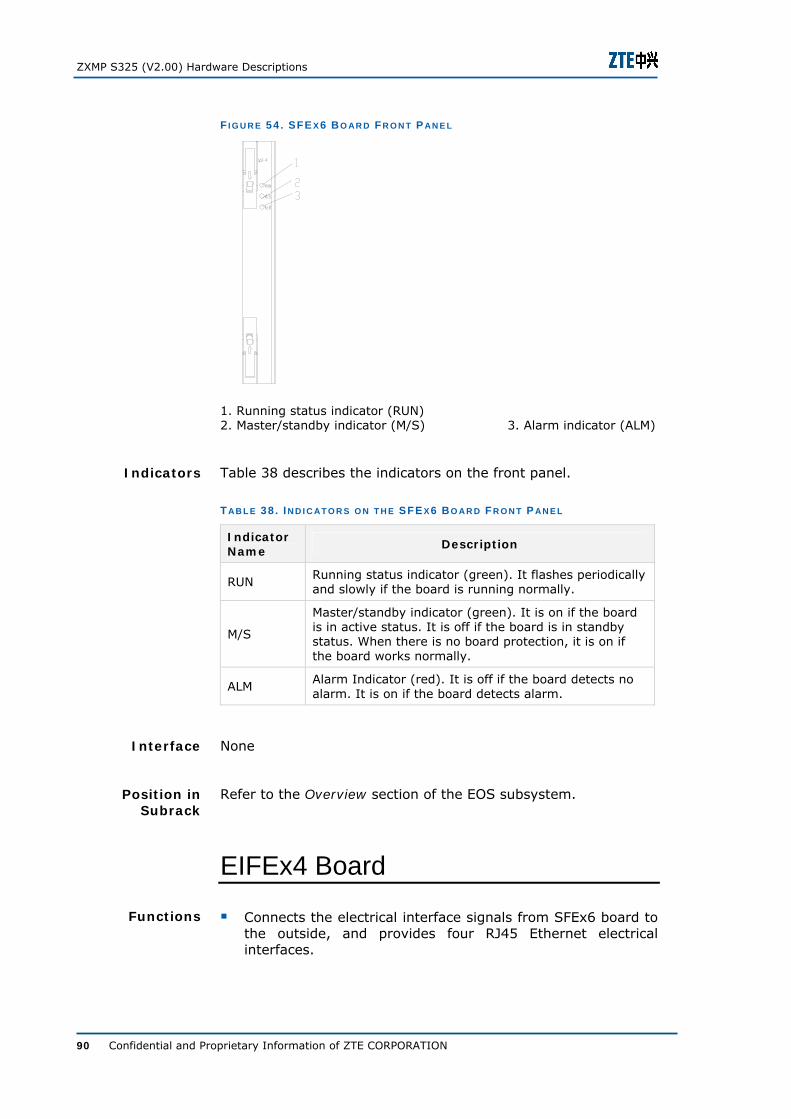
ZXMP S325 (V2.00) Hardware Descriptions
90 Confidential and Proprietary Information of ZTE CORPORATION
F I G U R E 54 . SFE X 6 B O AR D FR O N T P AN E L
1. Running status indicator (RUN) 2. Master/standby indicator (M/S) 3. Alarm indicator (ALM)
Table 38 describes the indicators on the front panel.
T AB L E 38 . I N D I C AT O R S O N T H E SFE X6 BO AR D FR O N T P AN E L
Indicator Name
Description
RUN Running status indicator (green). It flashes periodically and slowly if the board is running normally.
M/S
Master/standby indicator (green). It is on if the board is in active status. It is off if the board is in standby status. When there is no board protection, it is on if the board works normally.
ALM Alarm Indicator (red). It is off if the board detects no alarm. It is on if the board detects alarm.
None
Refer to the Overview section of the EOS subsystem.
EIFEx4 Board
Connects the electrical interface signals from SFEx6 board to the outside, and provides four RJ45 Ethernet electrical interfaces.
Indicators
Interface
Position in Subrack
Functions
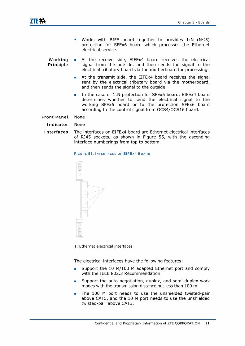
Chapter 3 - Boards
Confidential and Proprietary Information of ZTE CORPORATION 91
Works with BIFE board together to provides 1:N (N≤5) protection for SFEx6 board which processes the Ethernet electrical service.
At the receive side, EIFEx4 board receives the electrical signal from the outside, and then sends the signal to the electrical tributary board via the motherboard for processing.
At the transmit side, the EIFEx4 board receives the signal sent by the electrical tributary board via the motherboard, and then sends the signal to the outside.
In the case of 1:N protection for SFEx6 board, EIFEx4 board determines whether to send the electrical signal to the working SFEx6 board or to the protection SFEx6 board according to the control signal from OCS4/OCS16 board.
None
None
The interfaces on EIFEx4 board are Ethernet electrical interfaces of RJ45 sockets, as shown in Figure 55, with the ascending interface numberings from top to bottom.
F I G U R E 55 . I N T E R F AC E S O F E IFE X 4 B O AR D
1. Ethernet electrical interfaces
The electrical interfaces have the following features:
Support the 10 M/100 M adapted Ethernet port and comply with the IEEE 802.3 Recommendation
Support the auto-negotiation, duplex, and semi-duplex work modes with the transmission distance not less than 100 m.
The 100 M port needs to use the unshielded twisted-pair above CAT5, and the 10 M port needs to use the unshielded twisted-pair above CAT3.
Working Principle
Front Panel
Indicator
Interfaces
ZXMP S325 (V2.00) Hardware Descriptions
92 Confidential and Proprietary Information of ZTE CORPORATION
Refer to the Overview section of the EOS subsystem.
BIFE Board
BIFE board is the bridge interface board. It has the following functions:
Functions as a bridge between the protection SFEx6 board and the interface switching board (EIFEx4) corresponding to the faulty SFEx6 board.
Used only when 1:N (N≤5) protection for SFEx6 board is required.
Inserted in the interface board slot corresponding to the protection SFEx6 board.
The BIFE board bridges the service signal of its corresponding protection board to the public standby-signal pins on the motherboard.
None
None
None
Refer to the Overview section of the EOS subsystem.
Position in Subrack
Functions
Working Principle
Front Panel
Indicator
Interface
Position in Subrack
Chapter 3 - Boards
Confidential and Proprietary Information of ZTE CORPORATION 93
OIS1x4 Board
OIS1x4 board is the optical interface board. It has the following functions:
At the receive side, it converts the optical signal into electrical signal.
At the transmit side, it converts the electrical signal into optical signal.
Provides the service processing board (SFEx6 or AP1x4 board) with four optical receive interfaces and four optical transmit interfaces.
The optical transmit interfaces can shut down the laser automatically.
At the receive side, the board receives the optical signal inputted from the outside. Then it converts the 155 Mbit/s optical signal into electrical signal and extracts the line signal. Finally, it sends the processed electrical signal to the service processing board via the motherboard for further processing.
At the transmit side, the board receives the electrical signal sent by the service processing board via the motherboard. Then, it converts the electrical signal into the 155 Mbit/s optical signal. Finally, it transmits the optical signal to the outside.
None
None
The interfaces on the OIS1x4 board are Ethernet optical interfaces with LC/PC connectors, as shown in Figure 56, with the ascending interface numberings from top to bottom.
Functions
Working Principle
Front Panel
Indicator
Interfaces
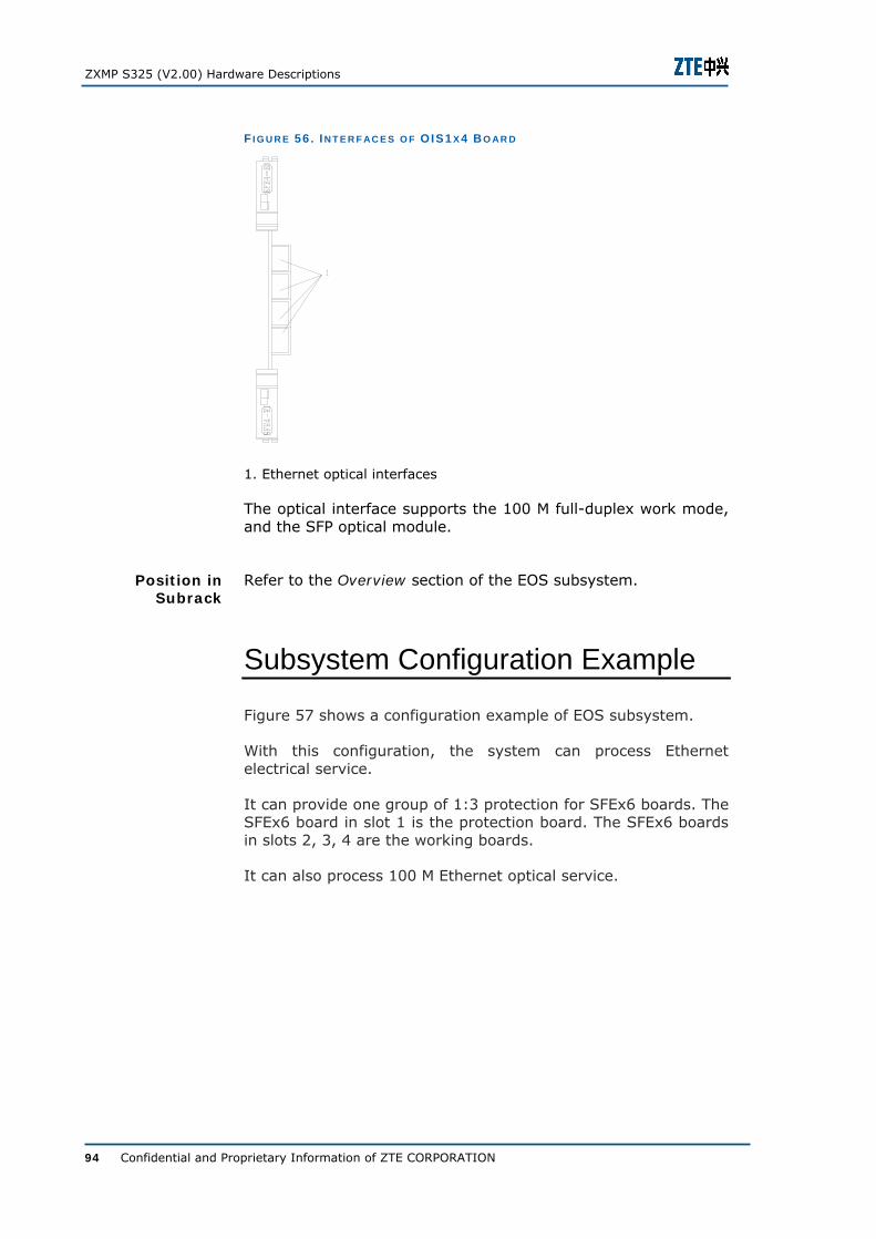
ZXMP S325 (V2.00) Hardware Descriptions
94 Confidential and Proprietary Information of ZTE CORPORATION
F I G U R E 56 . I N T E R F AC E S O F OIS1 X 4 B O AR D
1. Ethernet optical interfaces
The optical interface supports the 100 M full-duplex work mode, and the SFP optical module.
Refer to the Overview section of the EOS subsystem.
Subsystem Configuration Example
Figure 57 shows a configuration example of EOS subsystem.
With this configuration, the system can process Ethernet electrical service.
It can provide one group of 1:3 protection for SFEx6 boards. The SFEx6 board in slot 1 is the protection board. The SFEx6 boards in slots 2, 3, 4 are the working boards.
It can also process 100 M Ethernet optical service.
Position in Subrack
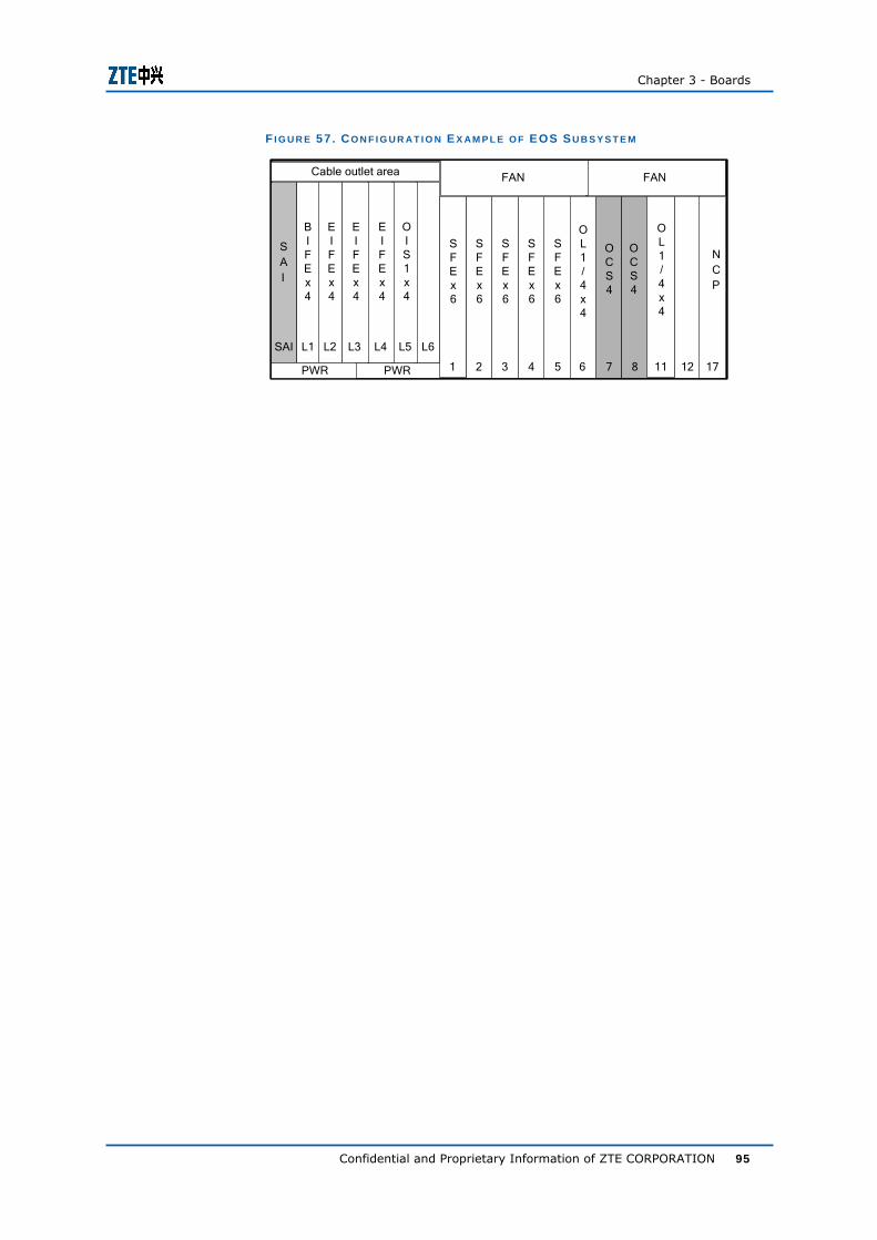
Chapter 3 - Boards
Confidential and Proprietary Information of ZTE CORPORATION 95
F I G U R E 57 . CO N F I G U R AT I O N E X AM P L E O F EOS SU B S Y S T E M
Cable outlet area
PWR 12 177 865432 111
FANFAN
L6L5L4L3L2L1SAI
NCP
SAI
OCS4
OCS4
PWR
BIFEx4
EIFEx4
EIFEx4
EIFEx4
SFEx6
OL1/4x4
OL1/4x4
SFEx6
SFEx6
SFEx6
OIS1x4
SFEx6
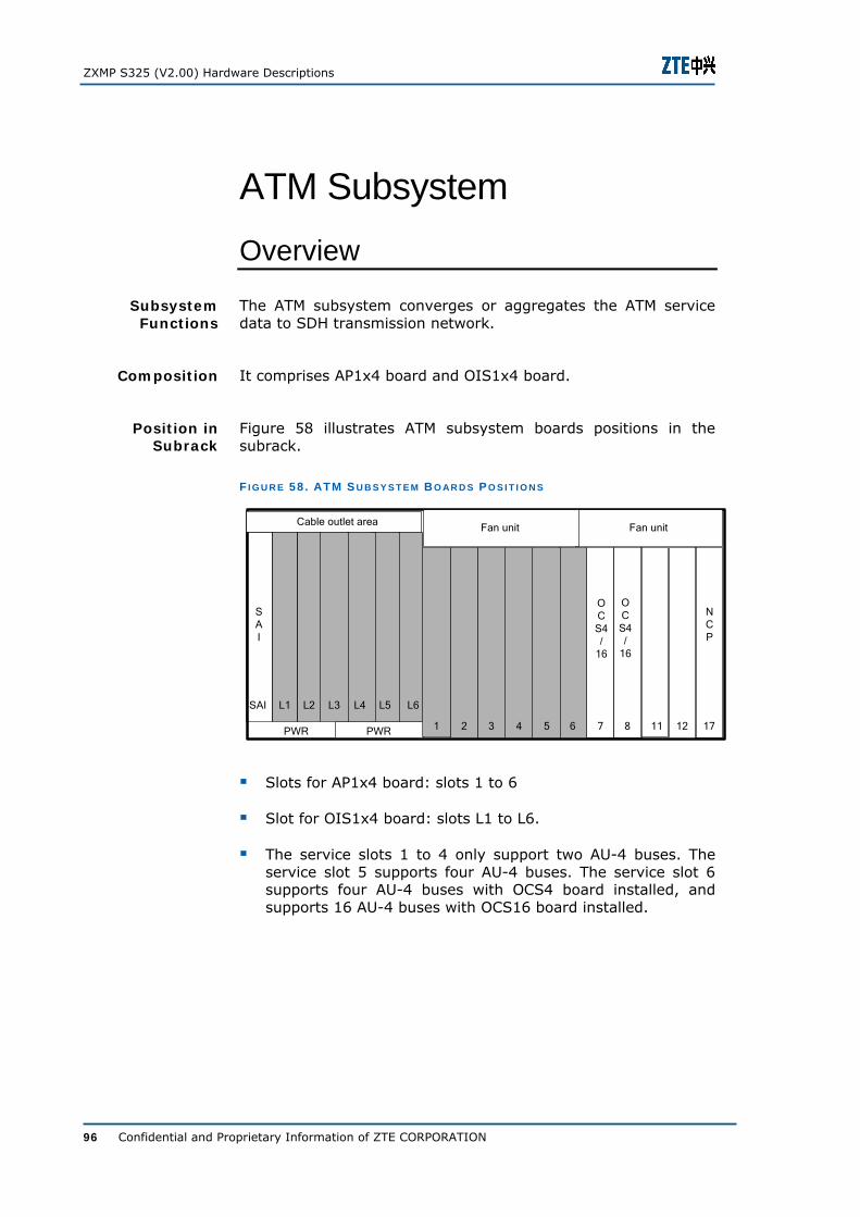
ZXMP S325 (V2.00) Hardware Descriptions
96 Confidential and Proprietary Information of ZTE CORPORATION
ATM Subsystem Overview
The ATM subsystem converges or aggregates the ATM service data to SDH transmission network.
It comprises AP1x4 board and OIS1x4 board.
Figure 58 illustrates ATM subsystem boards positions in the subrack.
F I G U R E 58 . ATM S U B S Y S T E M B O AR D S P O S I T I O N S
Cable outlet area
PWR PWR 12 177 865432 111
Fan unitFan unit
L6L5L4L3L2L1SAI
NCP
SAI
OCS4/
16
OCS4/
16
Slots for AP1x4 board: slots 1 to 6
Slot for OIS1x4 board: slots L1 to L6.
The service slots 1 to 4 only support two AU-4 buses. The service slot 5 supports four AU-4 buses. The service slot 6 supports four AU-4 buses with OCS4 board installed, and supports 16 AU-4 buses with OCS16 board installed.
Subsystem Functions
Composition
Position in Subrack
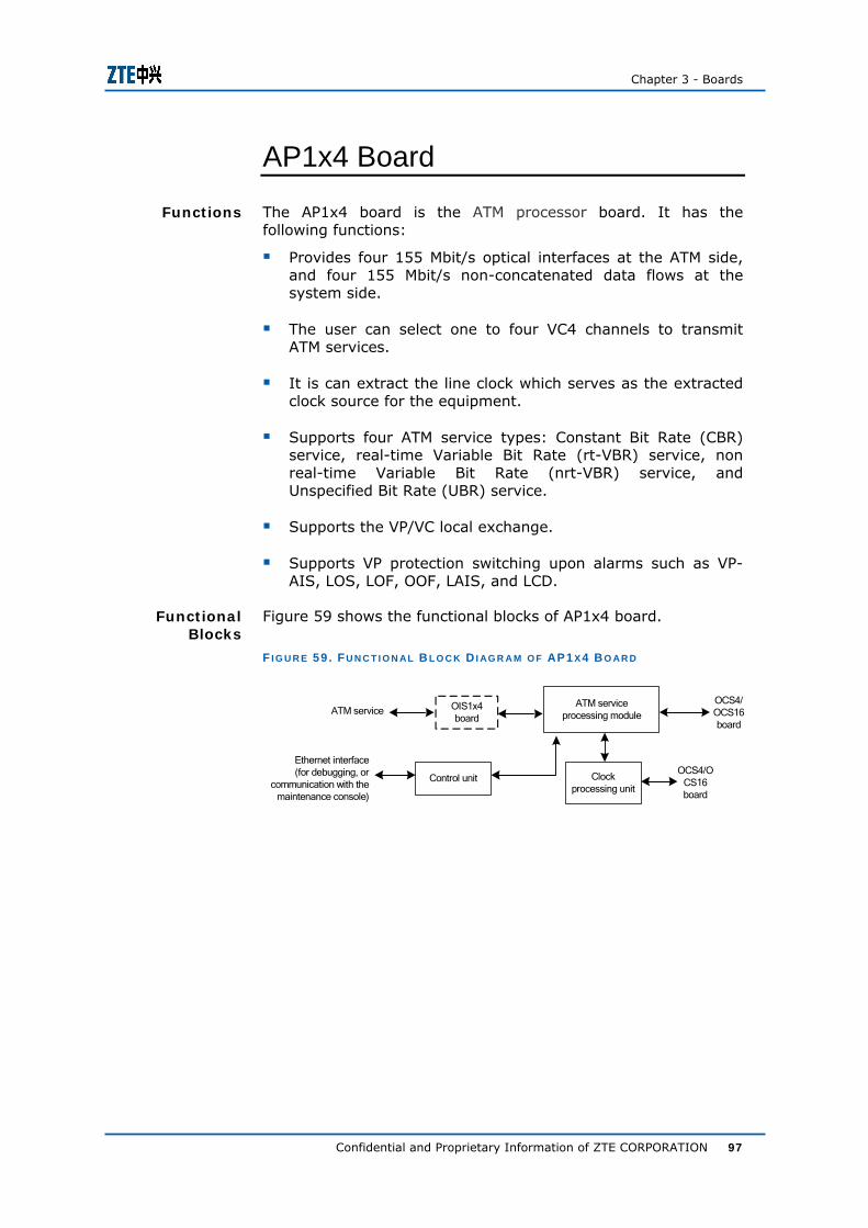
Chapter 3 - Boards
Confidential and Proprietary Information of ZTE CORPORATION 97
AP1x4 Board
The AP1x4 board is the ATM processor board. It has the following functions:
Provides four 155 Mbit/s optical interfaces at the ATM side, and four 155 Mbit/s non-concatenated data flows at the system side.
The user can select one to four VC4 channels to transmit ATM services.
It is can extract the line clock which serves as the extracted clock source for the equipment.
Supports four ATM service types: Constant Bit Rate (CBR) service, real-time Variable Bit Rate (rt-VBR) service, non real-time Variable Bit Rate (nrt-VBR) service, and Unspecified Bit Rate (UBR) service.
Supports the VP/VC local exchange.
Supports VP protection switching upon alarms such as VP-AIS, LOS, LOF, OOF, LAIS, and LCD.
Figure 59 shows the functional blocks of AP1x4 board.
F I G U R E 59 . FU N C T I O N AL B L O C K D I AG R A M O F AP1 X 4 B O AR D
OCS4/OCS16 board
Clock processing unit
ATM service processing module
Control unitOCS4/O
CS16 board
ATM service
Ethernet interface (for debugging, or
communication with the maintenance console)
OIS1x4 board
Functions
Functional Blocks
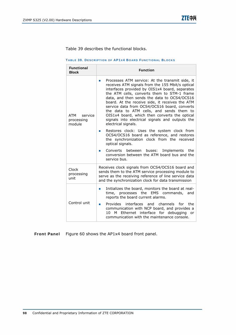
ZXMP S325 (V2.00) Hardware Descriptions
98 Confidential and Proprietary Information of ZTE CORPORATION
Table 39 describes the functional blocks.
T AB L E 39 . D E S C R I P T I O N O F AP1 X 4 B O AR D FU N C T I O N AL B L O C K S
Functional Block Function
ATM service processing module
Processes ATM service: At the transmit side, it receives ATM signals from the 155 Mbit/s optical interfaces provided by OIS1x4 board, separates the ATM cells, converts them to STM-1 frame data, and then sends the data to OCS4/OCS16 board. At the receive side, it receives the ATM service data from OCS4/OCS16 board, converts the data to ATM cells, and sends them to OIS1x4 board, which then converts the optical signals into electrical signals and outputs the electrical signals.
Restores clock: Uses the system clock from OCS4/OCS16 board as reference, and restores the synchronization clock from the received optical signals.
Converts between buses: Implements the conversion between the ATM board bus and the service bus.
Clock processing unit
Receives clock signals from OCS4/OCS16 board and sends them to the ATM service processing module to serve as the receiving reference of line service data and the synchronization clock for data transmission
Control unit
Initializes the board, monitors the board at real-time, processes the EMS commands, and reports the board current alarms.
Provides interfaces and channels for the communication with NCP board, and provides a 10 M Ethernet interface for debugging or communication with the maintenance console.
Figure 60 shows the AP1x4 board front panel. Front Panel
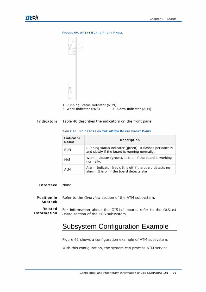
Chapter 3 - Boards
Confidential and Proprietary Information of ZTE CORPORATION 99
F I G U R E 60 . AP1 X 4 B O AR D FR O N T P AN E L
1. Running Status Indicator (RUN) 2. Work Indicator (M/S) 3. Alarm Indicator (ALM)
Table 40 describes the indicators on the front panel.
T AB L E 40 . I N D I C AT O R S O N T H E AP1 X 4 B O AR D FR O N T P AN E L
Indicator Name
Description
RUN Running status indicator (green). It flashes periodically and slowly if the board is running normally.
M/S Work indicator (green). It is on if the board is working normally.
ALM Alarm Indicator (red). It is off if the board detects no alarm. It is on if the board detects alarm.
None
Refer to the Overview section of the ATM subsystem.
For information about the OIS1x4 board, refer to the OIS1x4 Board section of the EOS subsystem.
Subsystem Configuration Example
Figure 61 shows a configuration example of ATM subsystem.
With this configuration, the system can process ATM service.
Indicators
Interface
Position in Subrack
Related Information
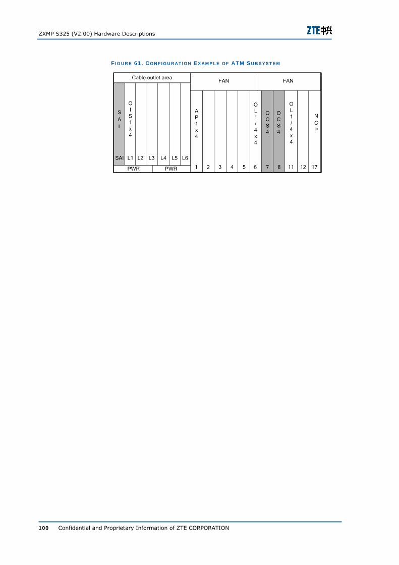
ZXMP S325 (V2.00) Hardware Descriptions
100 Confidential and Proprietary Information of ZTE CORPORATION
F I G U R E 61 . CO N F I G U R AT I O N E X AM P L E O F ATM S U B S Y S T E M
Cable outlet area
PWR 12 177 865432 111
FANFAN
L6L5L4L3L2L1SAI
NCP
SAI
OCS4
OCS4
PWR
OIS1x4
AP1x4
OL1/4x4
OL1/4x4
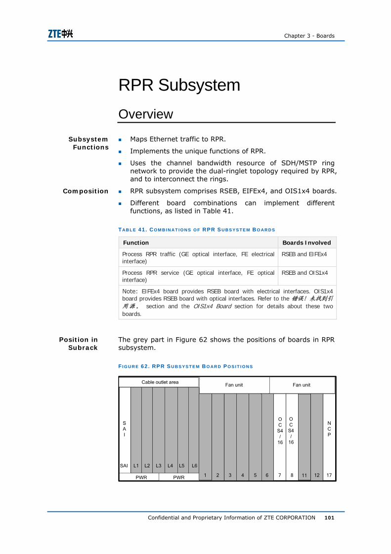
Chapter 3 - Boards
Confidential and Proprietary Information of ZTE CORPORATION 101
RPR Subsystem Overview
Maps Ethernet traffic to RPR.
Implements the unique functions of RPR.
Uses the channel bandwidth resource of SDH/MSTP ring network to provide the dual-ringlet topology required by RPR, and to interconnect the rings.
RPR subsystem comprises RSEB, EIFEx4, and OIS1x4 boards.
Different board combinations can implement different functions, as listed in Table 41.
T AB L E 41 . C O M B I N AT I O N S O F RPR S U B S Y S T E M B O AR D S
Function Boards Involved
Process RPR traffic (GE optical interface, FE electrical interface)
RSEB and EIFEx4
Process RPR service (GE optical interface, FE optical interface)
RSEB and OIS1x4
Note: EIFEx4 board provides RSEB board with electrical interfaces. OIS1x4 board provides RSEB board with optical interfaces. Refer to the 错误!未找到引用源。 section and the OIS1x4 Board section for details about these two boards.
The grey part in Figure 62 shows the positions of boards in RPR subsystem.
F I G U R E 62 . RPR S U B S Y S T E M B O AR D P O S I T I O N S
Cable outlet area
PWR PWR 12 177 8654321
Fan unitFan unit
L6L5L4L3L2L1SAI
NCP
SAI
OCS4/
16
OCS4/
16
11
Subsystem Functions
Composition
Position in Subrack
ZXMP S325 (V2.00) Hardware Descriptions
102 Confidential and Proprietary Information of ZTE CORPORATION
Slots for RSEB board: slots 1 to 6, slot 11, and slot 12 for service boards.
Slots for EIFEx4/OIS1x4 board: slots L1 to L6.
The service slots 1 to 4 only support two AU-4 buses. The service slot 5 supports four AU-4 buses. The service slot 6 supports four AU-4 buses with OCS4 board installed, and supports 16 AU-4 buses with OCS16 board installed.
RSEB Board
Supports the Q in Q identification; uses the outmost 802.1Q identifier as the VLAN identifier to isolate users; participates in learning, searching, and isolating traffic on the ring network.
Supports different users by identifying them with VID (VLAN ID). Every user can have multiple VLAN IDs, so that he can be completely isolated not only at local site but also between different sites, and thus satisfies the requirement of different user for data security.
Every user can have traffic of different priorities (including class A, B, and C). And VLAN ID varies with the traffic class.
The bandwidth and peak-value rate of traffic with a certain priority can be configured.
Supports the fairness algorithm.
Supports the topology discovery and protection function, and passthrough mode.
Supports the configuration of EMS, query of alarm and performance, and other queries (including port running status and RPR ring topology relation diagram).
The RPR ring bandwidth can be configure; supports VC4-xv and VC3-xv virtual concatenation; supports the bandwidth-adjustable RPR ring with granularity of VC-4.
Supports the Bypass RPR MAC function: traffic is only switched by Ethernet and is not switched by RPR MAC.
There are two kinds of RSEB board: RSEB-RPR and RSEB-EOS.
RSEB-RPR board is the ordinary RSEB board. It provides the RPR networking function.
RSEB-EOS board implements the pure EOS function with two GE interfaces (RPR system ports) by using Bypass RPR MAC switching.
Functions
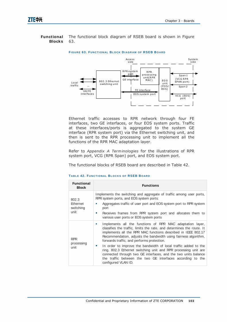
Chapter 3 - Boards
Confidential and Proprietary Information of ZTE CORPORATION 103
The functional block diagram of RSEB board is shown in Figure 63.
F I G U R E 63 . FU N C T I O N AL B L O C K D I AG R A M O F RSEB BO AR D
RPRproce ss ingunit (R PR
MAC)
Span 1
Span 2
802.3 Etherne tswitching unit
Loca ltra ffic
GE/FEinte rfaces
EO Sunit
(POS/EO S)
EO S system port
FE inte rface
RPR systemport
(VCG RPRSPAN po rt)
VCG (EOS)po rt
Accessside
Systemside
GE inte rfa ce
...
Ethernet traffic accesses to RPR network through four FE interfaces, two GE interfaces, or four EOS system ports. Traffic at these interfaces/ports is aggregated to the system GE interface (RPR system port) via the Ethernet switching unit, and then is sent to the RPR processing unit to implement all the functions of the RPR MAC adaptation layer.
Refer to Appendix A Terminologies for the illustrations of RPR system port, VCG (RPR Span) port, and EOS system port.
The functional blocks of RSEB board are described in Table 42.
T AB L E 42 . FU N C T I O N AL B L O C K S O F RSEB B O AR D
Functional Block Functions
802.3 Ethernet switching unit
Implements the switching and aggregate of traffic among user ports, RPR system ports, and EOS system ports: Aggregates traffic of user port and EOS system port to RPR system
port Receives frames from RPR system port and allocates them to
various user ports or EOS system ports
RPR processing unit
Implements all the functions of RPR MAC adaptation layer, classifies the traffic, limits the rate, and determines the route. It implements all the RPR MAC functions described in IEEE 802.17 Recommendation, adjusts the bandwidth using fairness algorithm, forwards traffic, and performs protection.
In order to improve the bandwidth of local traffic added to the ring, 802.3 Ethernet switching unit and RPR processing unit are connected through two GE interfaces, and the two units balance the traffic between the two GE interfaces according to the configured VLAN ID.
Functional Blocks
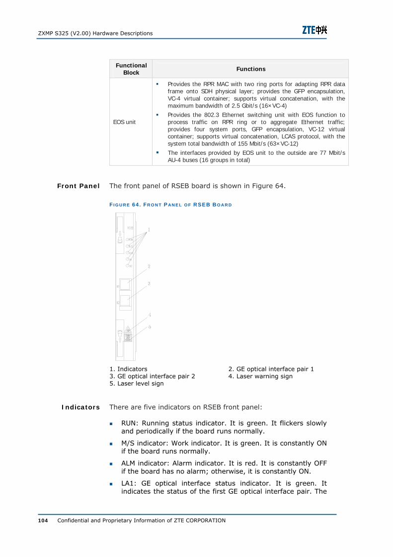
ZXMP S325 (V2.00) Hardware Descriptions
104 Confidential and Proprietary Information of ZTE CORPORATION
Functional Block Functions
EOS unit
Provides the RPR MAC with two ring ports for adapting RPR data frame onto SDH physical layer; provides the GFP encapsulation, VC-4 virtual container; supports virtual concatenation, with the maximum bandwidth of 2.5 Gbit/s (16×VC-4)
Provides the 802.3 Ethernet switching unit with EOS function to process traffic on RPR ring or to aggregate Ethernet traffic; provides four system ports, GFP encapsulation, VC-12 virtual container; supports virtual concatenation, LCAS protocol, with the system total bandwidth of 155 Mbit/s (63×VC-12)
The interfaces provided by EOS unit to the outside are 77 Mbit/s AU-4 buses (16 groups in total)
The front panel of RSEB board is shown in Figure 64.
F I G U R E 64 . FR O N T P AN E L O F RSEB B O AR D
1. Indicators 2. GE optical interface pair 1 3. GE optical interface pair 2 4. Laser warning sign 5. Laser level sign
There are five indicators on RSEB front panel:
RUN: Running status indicator. It is green. It flickers slowly and periodically if the board runs normally.
M/S indicator: Work indicator. It is green. It is constantly ON if the board runs normally.
ALM indicator: Alarm indicator. It is red. It is constantly OFF if the board has no alarm; otherwise, it is constantly ON.
LA1: GE optical interface status indicator. It is green. It indicates the status of the first GE optical interface pair. The
Front Panel
Indicators
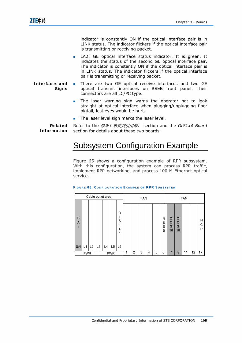
Chapter 3 - Boards
Confidential and Proprietary Information of ZTE CORPORATION 105
indicator is constantly ON if the optical interface pair is in LINK status. The indicator flickers if the optical interface pair is transmitting or receiving packet.
LA2: GE optical interface status indicator. It is green. It indicates the status of the second GE optical interface pair. The indicator is constantly ON if the optical interface pair is in LINK status. The indicator flickers if the optical interface pair is transmitting or receiving packet.
There are two GE optical receive interfaces and two GE optical transmit interfaces on RSEB front panel. Their connectors are all LC/PC type.
The laser warning sign warns the operator not to look straight at optical interface when plugging/unplugging fiber pigtail, lest eyes would be hurt.
The laser level sign marks the laser level.
Refer to the 错误!未找到引用源。 section and the OIS1x4 Board section for details about these two boards.
Subsystem Configuration Example
Figure 65 shows a configuration example of RPR subsystem. With this configuration, the system can process RPR traffic, implement RPR networking, and process 100 M Ethernet optical service.
F I G U R E 65 . CO N F I G U R AT I O N E X AM P L E O F RPR S U B S Y S T E M
Cable outlet area
PWR 12 177 865432 111
FANFAN
L6L5L4L3L2L1SAI
NCP
SAI
OCS16
OCS16
PWR
OIS1x4
RSEB
Interfaces and Signs
Related Information
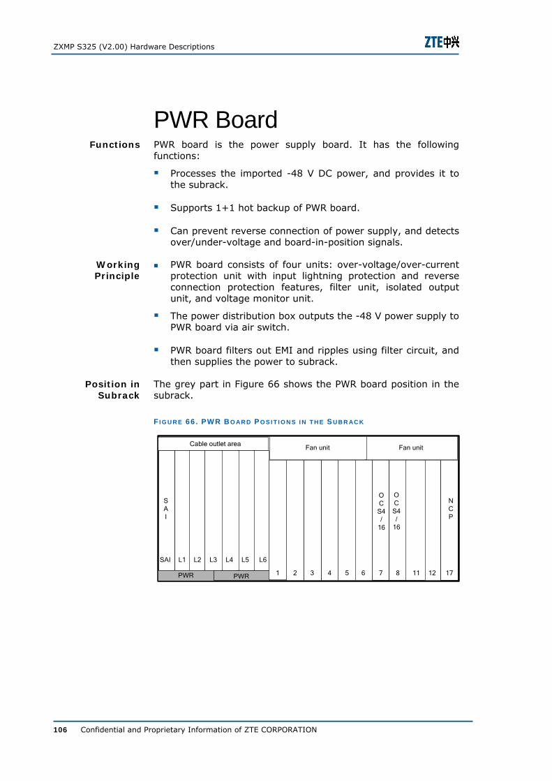
ZXMP S325 (V2.00) Hardware Descriptions
106 Confidential and Proprietary Information of ZTE CORPORATION
PWR Board PWR board is the power supply board. It has the following functions:
Processes the imported -48 V DC power, and provides it to the subrack.
Supports 1+1 hot backup of PWR board.
Can prevent reverse connection of power supply, and detects over/under-voltage and board-in-position signals.
PWR board consists of four units: over-voltage/over-current protection unit with input lightning protection and reverse connection protection features, filter unit, isolated output unit, and voltage monitor unit.
The power distribution box outputs the -48 V power supply to PWR board via air switch.
PWR board filters out EMI and ripples using filter circuit, and then supplies the power to subrack.
The grey part in Figure 66 shows the PWR board position in the subrack.
F I G U R E 66 . PWR B O AR D P O S I T I O N S I N T H E S U B R AC K
Cable outlet area
PWR 12 177 865432 111
Fan unitFan unit
L6L5L4L3L2L1SAI
NCP
SAI
OCS4/
16
OCS4/
16
PWR
Functions
Working Principle
Position in Subrack
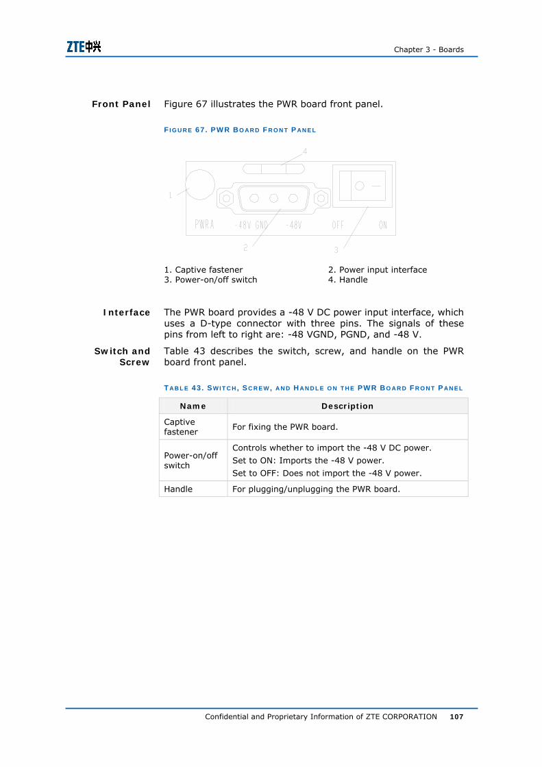
Chapter 3 - Boards
Confidential and Proprietary Information of ZTE CORPORATION 107
Figure 67 illustrates the PWR board front panel.
F I G U R E 67 . PWR B O AR D F R O N T P AN E L
1. Captive fastener 2. Power input interface 3. Power-on/off switch 4. Handle
The PWR board provides a -48 V DC power input interface, which uses a D-type connector with three pins. The signals of these pins from left to right are: -48 VGND, PGND, and -48 V.
Table 43 describes the switch, screw, and handle on the PWR board front panel.
T AB L E 43 . S W I T C H , S C R E W , AN D H AN D L E O N T H E PWR B O AR D FR O N T P AN E L
Name Description
Captive fastener
For fixing the PWR board.
Power-on/off switch
Controls whether to import the -48 V DC power.
Set to ON: Imports the -48 V power.
Set to OFF: Does not import the -48 V power.
Handle For plugging/unplugging the PWR board.
Front Panel
Interface
Switch and Screw

ZXMP S325 (V2.00) Hardware Descriptions
108 Confidential and Proprietary Information of ZTE CORPORATION
This page is intentionally blank.
Confidential and Proprietary Information of ZTE CORPORATION 109
A p p e n d i x A
Terminologies
1. EDFA
If an ordinary optical fiber is doped with some other element such as erbium or praseodymium, it would be able to amplify the laser at a certain waveband.
The full name of EDFA is Erbium Doped Fiber Amplifier. At the heart of the EDFA, the fiber is doped with erbium, a rare earth element that happens to have the appropriate energy levels in its atomic structure for amplifying light at 1550 nm. When light at 1550 nm travels through the erbium doped fiber, it causes stimulated emission. In this way, the 1550 nm optical input signal gains strength.
The basic components of EDFA include the gain medium (erbium doped fiber of various types), pump source, optical passive components (optical isolator, optical multiplexer, optical demultiplexer, optical fiber connector), control unit and control interface. Among which the optical isolator prevents reverse light from influencing the EDFA; the optical fiber connector facilitates the connections among EDFA, communication system, and optical lines; the optical coupler separates part of signals from the input and output optical lines, and sends these signals to the optical monitor.
2. RPR system port
It is also known as RPR port. For user data frames, the RPR ring network only has one entrance/exit. The RPR system port is actually a channel for RPR ring network to add/drop the user traffic. The traffic received at the RPR system port and sent to the user port is called the dropped traffic; while the traffic received at the user port and sent to the RPR system port is called the added traffic.
3. RPR Span port
It is also known as VCG (RPR Span) port. It refers to the port that supports reception/transmission of RPR frames from the 802.17 network. RPR has a dual-ring structure, which is similar to the topology of SDH bidirectional MS ring. It consists of two ringlets with opposite directions, among which the clockwise ringlet is called ring 0 and the counterclockwise ringlet is called ringlet 1. Each RPR ringlet
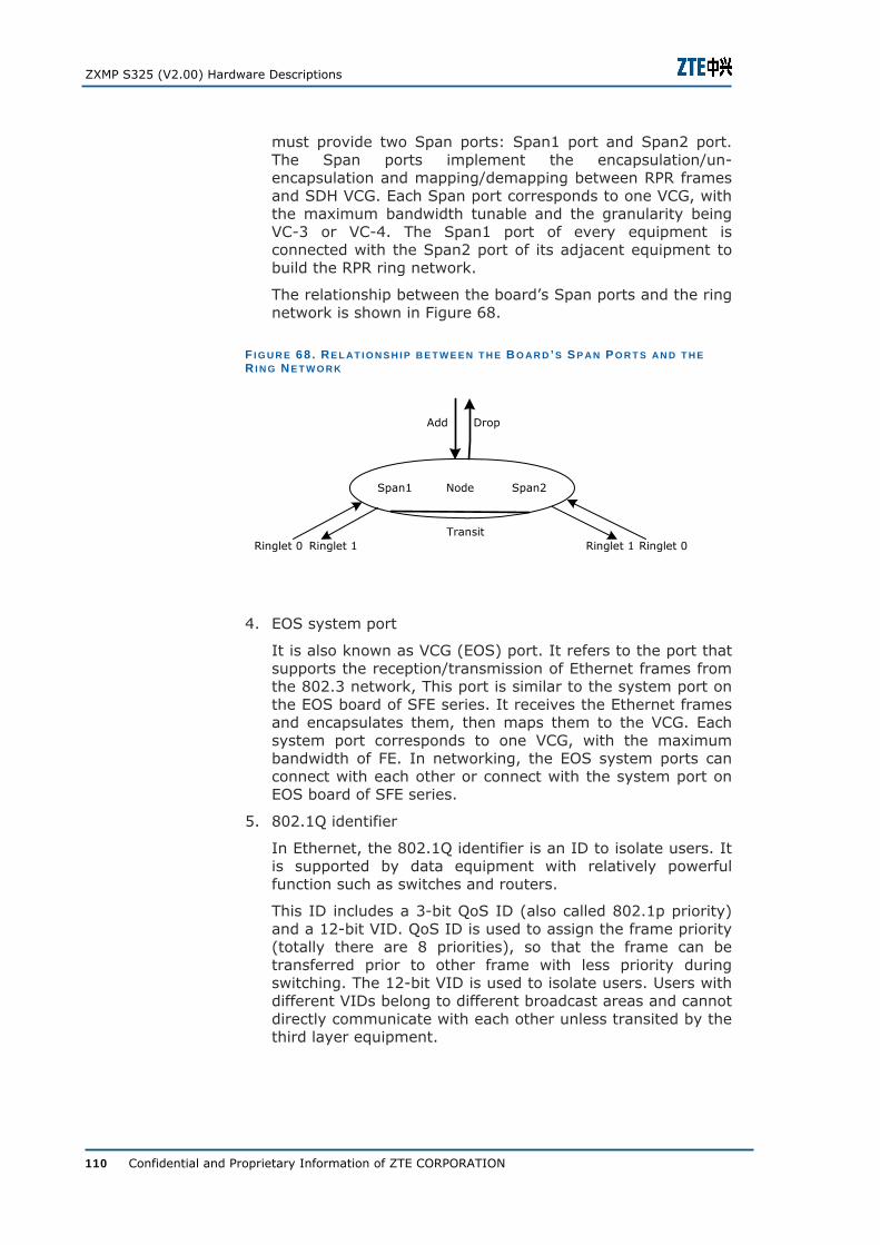
ZXMP S325 (V2.00) Hardware Descriptions
110 Confidential and Proprietary Information of ZTE CORPORATION
must provide two Span ports: Span1 port and Span2 port. The Span ports implement the encapsulation/un-encapsulation and mapping/demapping between RPR frames and SDH VCG. Each Span port corresponds to one VCG, with the maximum bandwidth tunable and the granularity being VC-3 or VC-4. The Span1 port of every equipment is connected with the Span2 port of its adjacent equipment to build the RPR ring network.
The relationship between the board’s Span ports and the ring network is shown in Figure 68.
F I G U R E 68 . RE L AT I O N S H I P B E T W E E N T H E B O AR D ’ S S P A N P O R T S AN D T H E R I N G N E T W O R K
Span1 Node Span2
Add Drop
TransitRinglet 1Ringlet 0 Ringlet 1 Ringlet 0
4. EOS system port
It is also known as VCG (EOS) port. It refers to the port that supports the reception/transmission of Ethernet frames from the 802.3 network, This port is similar to the system port on the EOS board of SFE series. It receives the Ethernet frames and encapsulates them, then maps them to the VCG. Each system port corresponds to one VCG, with the maximum bandwidth of FE. In networking, the EOS system ports can connect with each other or connect with the system port on EOS board of SFE series.
5. 802.1Q identifier
In Ethernet, the 802.1Q identifier is an ID to isolate users. It is supported by data equipment with relatively powerful function such as switches and routers.
This ID includes a 3-bit QoS ID (also called 802.1p priority) and a 12-bit VID. QoS ID is used to assign the frame priority (totally there are 8 priorities), so that the frame can be transferred prior to other frame with less priority during switching. The 12-bit VID is used to isolate users. Users with different VIDs belong to different broadcast areas and cannot directly communicate with each other unless transited by the third layer equipment.

Appendix A - Terminologies
Confidential and Proprietary Information of ZTE CORPORATION 111
6. Q in Q
It is 802.1Q in 802.1Q. It refers to adding one layer of 802.1Q ID in front of the existed user 802.1Q ID, and isolating users of the same operator without modifying the original user ID, thus implementing the two-layer isolation (the user uses one isolation layer, and the operator uses the other one). This method is also called the Vlan Stack or Double Vlan.

ZXMP S325 (V2.00) Hardware Descriptions
112 Confidential and Proprietary Information of ZTE CORPORATION
This page is intentionally blank.
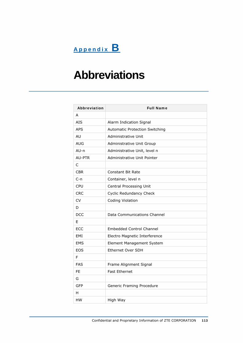
Confidential and Proprietary Information of ZTE CORPORATION 113
A p p e n d i x B
Abbreviations
Abbreviation Full Name
A
AIS Alarm Indication Signal
APS Automatic Protection Switching
AU Administrative Unit
AUG Administrative Unit Group
AU-n Administrative Unit, level n
AU-PTR Administrative Unit Pointer
C
CBR Constant Bit Rate
C-n Container, level n
CPU Central Processing Unit
CRC Cyclic Redundancy Check
CV Coding Violation
D
DCC Data Communications Channel
E
ECC Embedded Control Channel
EMI Electro Magnetic Interference
EMS Element Management System
EOS Ethernet Over SDH
F
FAS Frame Alignment Signal
FE Fast Ethernet
G
GFP Generic Framing Procedure
H
HW High Way
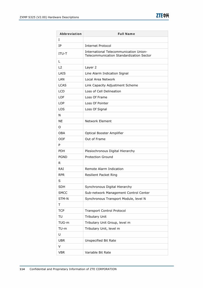
ZXMP S325 (V2.00) Hardware Descriptions
114 Confidential and Proprietary Information of ZTE CORPORATION
Abbreviation Full Name
I
IP Internet Protocol
ITU-T International Telecommunication Union-Telecommunication Standardization Sector
L
L2 Layer 2
LAIS Line Alarm Indication Signal
LAN Local Area Network
LCAS Link Capacity Adjustment Scheme
LCD Loss of Cell Delineation
LOF Loss Of Frame
LOP Loss Of Pointer
LOS Loss Of Signal
N
NE Network Element
O
OBA Optical Booster Amplifier
OOF Out of Frame
P
PDH Plesiochronous Digital Hierarchy
PGND Protection Ground
R
RAI Remote Alarm Indication
RPR Resilient Packet Ring
S
SDH Synchronous Digital Hierarchy
SMCC Sub-network Management Control Center
STM-N Synchronous Transport Module, level N
T
TCP Transport Control Protocol
TU Tributary Unit
TUG-m Tributary Unit Group, level m
TU-m Tributary Unit, level m
U
UBR Unspecified Bit Rate
V
VBR Variable Bit Rate
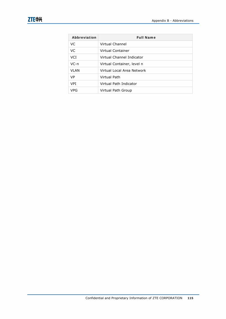
Appendix B - Abbreviations
Confidential and Proprietary Information of ZTE CORPORATION 115
Abbreviation Full Name
VC Virtual Channel
VC Virtual Container
VCI Virtual Channel Indicator
VC-n Virtual Container, level n
VLAN Virtual Local Area Network
VP Virtual Path
VPI Virtual Path Indicator
VPG Virtual Path Group

ZXMP S325 (V2.00) Hardware Descriptions
116 Confidential and Proprietary Information of ZTE CORPORATION
This page is intentionally blank.
Confidential and Proprietary Information of ZTE CORPORATION 117
Figures
Figure 1. ZXMP S325 Cabinets Outlines .................................6
Figure 2. Basic Fittings of a 2200 mm High ZXMP S325 Cabinet 7
Figure 3. Grounding Terminals and Grounding Copper Busbar of ZXMP S325 Cabinet ............................................................9
Figure 4. Structural Parts of ZXMP S325 .............................. 11
Figure 5. Subrack Structure ............................................... 15
Figure 6. Structure of Fan Box............................................ 17
Figure 7. Structure of Dustproof Unit................................... 18
Figure 8. Structure of Power Distribution Box ....................... 19
Figure 9. Pins of DB9 (Female) Socket................................. 20
Figure 10. Board Slots of ZXMP S325 Subrack ...................... 27
Figure 11. Structures of Electrical Interface/Switching Board and Optical Interface Board ..................................................... 28
Figure 12. OCS4 Board Structure ........................................ 29
Figure 13. Motherboard Structure Diagram........................... 30
Figure 14. NCP and SAI Boards Positions in a Subrack ........... 31
Figure 15. Functional Block Diagram of NCP Board ................ 33
Figure 16. NCP Board Front Panel ....................................... 34
Figure 17. Functional Block Diagram of SAI Board ................. 36
Figure 18. SAI Board Interfaces.......................................... 37
Figure 19. Position of Cross-connect and Clock Unit............... 39
Figure 20. Capacity Distribution of Motherboard Equipped with OCS16 Board ................................................................... 41
Figure 21. Functional Block Diagram of OCS16 Board............. 42
Figure 22. OCS16 Board Front Panel ................................... 43
Figure 23. Capacity Distribution of Motherboard Equipped with STM-4 OCS4 Board........................................................... 46
Figure 24. Functional Block Diagram of OCS4 Board .............. 47
Figure 25. OCS4 Board Front Panel ..................................... 48
Figure 26. Functional Block Diagram of OL16x1 Board ........... 50
Figure 27. Front Panel of OL16x1 Board............................... 51
ZXMP S325 (V2.00) Hardware Descriptions
118 Confidential and Proprietary Information of ZTE CORPORATION
Figure 28. Position of OL16x1 Board in Subrack .................... 52
Figure 29. Functional Block Diagram of OL1/4x4 Board .......... 53
Figure 30. Front Panel of OL1/4x4 Board ............................. 54
Figure 31. Positions of OL1/4x4 Board in ZXMP S325 Subrack. 55
Figure 32. Positions of Boards in the OL1/4 Subsystem.......... 58
Figure 33. Functional Block Diagram of LP1x1/LP1x2/LP4x1/LP4x2 Boards ...................................... 59
Figure 34. LP1x1/LP1x2/LP4x1/LP4x2 Board Front Panel ........ 60
Figure 35. OIS1x2 Board Interfaces .................................... 62
Figure 36. ESS1x2 Board Interfaces .................................... 64
Figure 37. Configuration Example of OL1/4 Subsystem .......... 65
Figure 38. Connection Relations among OA Board and Other Boards............................................................................ 66
Figure 39. Functional Block Diagram of OA Board.................. 67
Figure 40. Front Panel of OBA Board ................................... 68
Figure 41. Available Slots of OA Board................................. 69
Figure 42. Positions of EP1 Subsystem Boards ...................... 71
Figure 43. Functional Block Diagram of EPE1x21/EPT1x21/EPE1B Boards............................................................................ 72
Figure 44. Front Panel of EPE1x21/EPT1x21/EPE1B Board ...... 73
Figure 45. ESE1x21 Board Interface.................................... 76
Figure 46. Configuration Example of EP1 Subsystem ............. 78
Figure 47. EP3 Subsystem Board Positions ........................... 79
Figure 48. Functional Block Diagram of EP3x3 Board ............. 81
Figure 49. Front Panel of EP3x3 Board................................. 82
Figure 50. ESE3x3 Board Interfaces .................................... 83
Figure 51. Configuration Example of EP3 Subsystem ............. 85
Figure 52. EOS Subsystem Board Positions .......................... 87
Figure 53. Functional Block Diagram of SFEx6 Board ............. 88
Figure 54. SFEx6 Board Front Panel .................................... 90
Figure 55. Interfaces of EIFEx4 Board ................................. 91
Figure 56. Interfaces of OIS1x4 Board................................. 94
Figure 57. Configuration Example of EOS Subsystem............. 95
Figure 58. ATM Subsystem Boards Positions ......................... 96
Figure 59. Functional Block Diagram of AP1x4 Board ............. 97
Figure 60. AP1x4 Board Front Panel .................................... 99
Figure 61. Configuration Example of ATM Subsystem........... 100
Appendix B - Abbreviations
Confidential and Proprietary Information of ZTE CORPORATION 119
Figure 62. RPR Subsystem Board Positions......................... 101
Figure 63. Functional Block Diagram of RSEB Board............. 103
Figure 64. Front Panel of RSEB Board ................................ 104
Figure 65. Configuration Example of RPR Subsystem ........... 105
Figure 66. PWR Board Positions in the Subrack ................... 106
Figure 67. PWR Board Front Panel..................................... 107
Figure 68. Relationship between the Board’s Span Ports and the Ring Network................................................................. 110

ZXMP S325 (V2.00) Hardware Descriptions
120 Confidential and Proprietary Information of ZTE CORPORATION
This page is intentionally blank.
Confidential and Proprietary Information of ZTE CORPORATION 121
Tables
Table 1. Chapter Summary ...................................................i
Table 2. Typographical Conventions ...................................... ii
Table 3. Mouse Operation Conventions ................................. iii
Table 4. Cabinet Dimensions and Weights ..............................5
Table 5. ZXMP S325 Basic Fitting Descriptions ........................8
Table 6. Configuration of ZXMP S325 in a Single Cabinet........ 10
Table 7. Dimensions and Weights of ZXMP S325 Structural Parts..................................................................................... 11
Table 8. Brief Descriptions of Different Subrack Parts............. 15
Table 9. Signal Definitions of DB9 (Female) Socket................ 20
Table 10. Units and Subsystems of ZXMP S325..................... 23
Table 11. ZXMP S325 Boards ............................................. 24
Table 12. Description of NCP Board Functional Blocks ............ 33
Table 13. Indicators on NCP Board Front Panel ..................... 35
Table 14. Interfaces and Buttons on NCP Board Front Panel.... 35
Table 15. Description of SAI Board Functional Blocks ............. 36
Table 16. Descriptions of SAI Board Interfaces ..................... 38
Table 17. Description of OCS16 Board Functional Blocks ........ 42
Table 18. Indicators on OCS16 Board Front Panel.................. 44
Table 19. Description of OCS4 Board Functional Blocks .......... 47
Table 20. Indicators on OCS4 Board Front Panel ................... 49
Table 21. Functional Blocks of OL16x1 Board........................ 50
Table 22. Functional Blocks of OL1/4x4 Board....................... 53
Table 23. Descriptions of OL1/4x4 Board Positions in ZXMP S325 Subrack .......................................................................... 55
Table 24. Board Combinations in OL1/4 Subsystem............... 57
Table 25. Available Slots for Boards in the OL1/4 Subsystem .. 58
Table 26. Description of LP1x1/LP1x2/LP4x1/LP4x2 Board Functional Blocks.............................................................. 60
ZXMP S325 (V2.00) Hardware Descriptions
122 Confidential and Proprietary Information of ZTE CORPORATION
Table 27. Indicators on the LP1x1/LP1x2/LP4x1 Board Front Panel .............................................................................. 61
Table 28. Description of OA Board Functional Blocks.............. 67
Table 29. Combinations of Boards in EP1 Subsystem ............. 70
Table 30. Description of EPE1x21/EPT1x21/EPE1B Board Functional Blocks.............................................................. 72
Table 31. Indicators on the EPE1x21/EPT1x21/EPE1B Board Front Panel...................................................................... 74
Table 32. Pin Signal Definitions of ESE1x21 Board Electrical Interface......................................................................... 76
Table 33. Combination of Boards in EP3 Subsystem............... 79
Table 34. Functional Blocks of EP3x3 Board.......................... 81
Table 35. Indicators on EP3x3 Board Front Panel .................. 82
Table 36. Combinations of Boards in EOS Subsystem............. 86
Table 37. Description of SFEx6 Board Functional Blocks ......... 89
Table 38. Indicators on the SFEx6 Board Front Panel ............. 90
Table 39. Description of AP1x4 Board Functional Blocks ......... 98
Table 40. Indicators on the AP1x4 Board Front Panel ............. 99
Table 41. Combinations of RPR Subsystem Boards .............. 101
Table 42. Functional Blocks of RSEB Board......................... 103
Table 43. Switch, Screw, and Handle on the PWR Board Front Panel ............................................................................ 107