Embed Size (px)
Citation preview
AFRL-RX-WP-TP-2010-4294
ELECTRONMAGNETIC CHARACTERIZATION OF CARBON NANOTUBE FILMS SUBJECT TO AN OXIDATIVE TREATMENT AT ELEVATED TEMPERATURE (Preprint) John J. Boeckl, Angela L. Campbell, and Timothy L. Peterson
Electronic and Optical Materials Branch Survivability and Sensor Materials Division Richard A. Kleismit, Kineshma Munbodh, and Gregory Kozlowski
Wright State University Krzysztof K. Koziol
University of Cambridge
JULY 2010 Interim Report
Approved for public release; distribution unlimited.
See additional restrictions described on inside pages
STINFO COPY
AIR FORCE RESEARCH LABORATORY MATERIALS AND MANUFACTURING DIRECTORATE
WRIGHT-PATTERSON AIR FORCE BASE, OH 45433-7750 AIR FORCE MATERIEL COMMAND
UNITED STATES AIR FORCE
i
REPORT DOCUMENTATION PAGE Form Approved
OMB No. 0704-0188
The public reporting burden for this collection of information is estimated to average 1 hour per response, including the time for reviewing instructions, existing data sources, gathering and maintaining the data needed, and completing and reviewing the collection of information. Send comments regarding this burden estimate or any other aspect of this collection of information, including suggestions for reducing this burden, to Department of Defense, Washington Headquarters Services, Directorate for Information Operations and Reports (0704-0188), 1215 Jefferson Davis Highway, Suite 1204, Arlington, VA 22202-4302. Respondents should be aware that notwithstanding any other provision of law, no person shall be subject to any penalty for failing to comply with a collection of information if it does not display a currently valid OMB control number. PLEASE DO NOT RETURN YOUR FORM TO THE ABOVE ADDRESS.
1. REPORT DATE (DD-MM-YY) 2. REPORT TYPE 3. DATES COVERED (From - To)
July 2010 Journal Article Preprint 27 January 2006 – 26 June 2010 4. TITLE AND SUBTITLE
ELECTRONMAGNETIC CHARACTERIZATION OF CARBON NANOTUBE FILMS SUBJECT TO AN OXIDATIVE TREATMENT AT ELEVATED TEMPERATURE (Preprint)
5a. CONTRACT NUMBER
IN-HOUSE 5b. GRANT NUMBER
5c. PROGRAM ELEMENT NUMBER
62102F 6. AUTHOR(S)
John J. Boeckl, Angela L. Campbell, and Timothy L. Peterson (Survivability and Sensor Materials Division, Electronic and Optical Materials Branch (AFRL/RXPS)) Richard A. Kleismit, Kineshma Munbodh, and Gregory Kozlowski (Wright State University) Krzysztof K. Koziol (University of Cambridge)
5d. PROJECT NUMBER
4348 5e. TASK NUMBER
RG 5f. WORK UNIT NUMBER
M07R5000
7. PERFORMING ORGANIZATION NAME(S) AND ADDRESS(ES) 8. PERFORMING ORGANIZATION
REPORT NUMBER Electronic and Optical Materials Branch Survivability and Sensor Materials Division Materials and Manufacturing Directorate Wright-Patterson Air Force Base, OH 45433-7750 Air Force Materiel Command, United States Air Force
Wright State University Physics Department AFRL-RX-WP-TP-2010-4294
University of Cambridge Department of Materials Science and
Metallurgy
9. SPONSORING/MONITORING AGENCY NAME(S) AND ADDRESS(ES) 10. SPONSORING/MONITORING AGENCY ACRONYM(S)
Air Force Research Laboratory Materials and Manufacturing Directorate Wright-Patterson Air Force Base, OH 45433-7750 Air Force Materiel Command United States Air Force
AFRL/RXPS 11. SPONSORING/MONITORING AGENCY REPORT NUMBER(S)
AFRL-RX-WP-TP-2010-4294
12. DISTRIBUTION/AVAILABILITY STATEMENT
Approved for public release; distribution unlimited.
13. SUPPLEMENTARY NOTES
PAO case number 88ABW-2010-3440, cleared 22 June 2010. The U.S. Government is joint author of this work and has the right to use, modify, reproduce, release, perform, display, or disclose the work. To be published in Journal Nanosci. Nanotechnol., 2009 Aug;9(8):4543-53. Document contains color.
14. ABSTRACT
Electromagnetic characterization of carbon nanotube (CNT) films fabricated by thermal decomposition of silicon carbide (SiC) has been performed. Purification and/or uncapping treatment conditions at an elevated temperature of 400 °C under flowing oxygen or carbon dioxide have been studied. A near field microwave microscope was used to measure the real and imaginary parts of the complex permittivity of CNT films through the frequency shift and the change in reciprocal quality factor between two extreme positions of an evanescent microwave probe-tip (in contact with the sample, and away from interaction with it). A theoretical two-point model was proposed to confirm experimental data, which showed poor conductivity of the CNT film as grown but has slight improvement after 40-minute treatment.
15. SUBJECT TERMS
evanescent microwave microscopy, permittivity, quality factor, purification and uncapping of carbon nanotubes
16. SECURITY CLASSIFICATION OF: 17. LIMITATION OF ABSTRACT:
SAR
18. NUMBER OF PAGES
32
19a. NAME OF RESPONSIBLE PERSON (Monitor)
a. REPORT Unclassified
b. ABSTRACT Unclassified
c. THIS PAGE Unclassified
Charles Stutz 19b. TELEPHONE NUMBER (Include Area Code)
N/A
Standard Form 298 (Rev. 8-98) Prescribed by ANSI Std. Z39-18
1
Electromagnetic characterization of carbon nanotube films subject to an
oxidative treatment at elevated temperature
Richard A. Kleismit1, Kineshma Munbodh1, John J. Boeckl2, Angela L. Campbell2, Krzysztof K. Koziol3,
Gregory Kozlowski1,3, Simon C. Hopkins3, and Timothy L. Peterson2
1 Physics Department, Wright State University, Dayton, OH 45435, U.S.A. 2 Materials and Manufacturing Directorate, Air Force Research Laboratory, Wright- Patterson AFB, OH 45433, U.S.A. 3 Department of Materials Science and Metallurgy, University of Cambridge, Pembroke Street, Cambridge, CB2 3QZ, UK
E-mail: [email protected] ABSTRACT
Electromagnetic characterization of CNT films fabricated by thermal decomposition
of SiC has been performed. Purification and/or uncapping treatment conditions at an
elevated temperature of 400°C under flowing oxygen or carbon dioxide have been
studied. A near field microwave microscope was used to measure the real and imaginary
parts of the complex permittivity of CNT films through the frequency shift and the
change in reciprocal quality factor between two extreme positions of an evanescent
2
microwave probe-tip (in contact with the sample, and away from interaction with it). A
theoretical two-point model was proposed to confirm experimental data, which showed
poor conductivity of the CNT film as grown but has slight improvement after 40 min
treatment.
Key words: evanescent microwave microscopy, permittivity, quality factor, purification
and uncapping of carbon nanotubes
INTRODUCTION
Carbon nanotubes (CNTs) have attracted a lot of attention since their discovery in
1991 by Iijima [1]. They are used in a variety of applications from nanoelectronics
through microwave amplification to sensors. Assemblies of nanotubes in the form of
films or carpets can be used as flat panel displays or lighting elements (e.g., the
brightness of CNT arrays is higher by a factor of two than conventional thermionic
lighting elements for giant outdoor displays). CNTs grown by arc-discharge, laser
ablation and chemical vapor deposition (CVD) can appear in a large variety of forms [2]-
[4]. Single-walled nanotubes (SWNTs) have a mean diameter of one nanometer, lengths
that can reach several microns, and end in a spherical cap. The lengths of multi-walled
nanotubes (MWNTs) are usually well over 10 μm with diameters up to 70 nm [5]-[18],
and they show tips with a polyhedral shape. Finally, nanotubes produced by catalytic
reactions often show partially ordered layers containing extended structural defects. The
relatively small diameter of CNTs is very favorable for field emitters, devices based on
the process by which a substance emits electrons when an electric field or voltage is
applied to it. The electric field has to be very high, in the order of 107 V/cm. To reach
this value, the field amplification effect is very helpful: namely, the electric field lines are
concentrated more densely around a sharp object (e.g., the tip of the CNTs). Nanotubes
ensure very high field amplification because of their elongated shape. The maximum
current drawn from one single-walled nanotube is ~ 0.2 mA and from multi-walled
nanotube ~ 0.1 mA. It appears that open tubes are far less efficient emitters than closed
ones: the voltage needed for emission is typically a factor of two higher for open
3
nanotubes. This is a surprising result since the smaller effective curvature of the open
nanotubes was expected to lead to larger field amplification. However, it is now thought
that oxygen atoms attract themselves to the free dangling bond at the ends of the
nanotube, resulting in localized electron states. Since these states lie well below the
Fermi energy in the nanotube, they cannot emit electrons. Localized states are formed
also at the tips of closed nanotubes but these states are coupled to π-orbitals, effectively
enhancing the emission of electrons [13]. Useful parameters for a comparison of the field
emission performances of the different types of nanotube are the turn-on field (ranging
from 0.4 V/μm to 7.5 V/μm) and the threshold field (from 0.9 V/μm up), i.e., the electric
fields needed to produce current densities of 10 μA/cm2 and 10 mA/cm2, respectively [9]-
[13].
For multi-stage carbon nanotube emitters grown on porous silicon by the CVD
method (the average length and diameter of the SWNTs and thin MWNTs were ~ 10 μm
– 15 μm and ~ 2 nm – 10 nm, respectively) the turn-on field and current at a field of
1 V/μm were ~ 0.4 V/μm, 0.6 V/μm and ~ 450 μA, 14 μA, respectively [15].
Liu et al. [17] reported field emission measurements on CNTs grown on silicon
nanowire arrays by the CVD method, with turn-on field and threshold field respectively
equal to 2.3 V/μm and 3.2 V/μm. The voltages needed for a given emission current are
typically a factor of two higher for open tubes: the voltage increased from 190 V to
400 V, and from 320 V to 570 V, for 10 nA and 10 A emission, respectively.
There is a significant difference in the field emission characteristics between single-
walled, closed and open arc-discharge multi-walled, and catalytically grown multi-walled
nanotubes. To obtain low operating voltages as well as long emitter lifetimes, the
nanotubes should be multi-walled and have closed, well graphitized tips. The optimal
emitters are thus closed arc-grown MWNTs. SWNTs degrade substantially faster, as do
MWNTs with disordered structures, in addition to requiring high voltages for emission.
Finally, the emission performance of MWNT nanotubes is seriously degraded by opening
their ends.
Nanotube films (carpets) display the lowest emission voltage for closed MWNT
films, followed by closed SWNTs, opened MWNTs and SWNTs. A much more
4
homogeneous emission image is obtained for a medium-density nanotube film primarily
due to the large number of emitting sites involved and above all the smaller screening
effects. One of the factors for efficient field emission is the distance between CNTs,
which should be greater than their height to minimize the electric field screening effect
[18]. Taking into account the appropriate lengths of the tubes and the distances between
neighboring emitters, sufficient field amplification can be reached in these films. To
obtain low operating voltages as well as long emitter lifetimes, the CNT films should be
multi-walled and have closed, well-ordered tips.
The field emission behavior of carbon nanotubes cannot be understood solely by
assuming emission from metallic tips. The luminescence and measurements of the energy
distribution of the emitted electrons indicate that the electrons are emitted from states in a
narrow band of ~ 0.3 eV half-width. In fact, theoretical calculations show that the local
density of states at the tip presents sharp localized states that are correlated to the
presence of pentagonal defects [13]. The observed luminescence strongly suggests that
although the greatest part of the emitted current comes from occupied states with a large
density of states near the Fermi level, other, deeper levels also contribute to the field
emission. The position of the tip states with respect to the Fermi level influences directly
the field emission properties of the tube. Indeed, only tubes with a band state just under
or over the Fermi level are good candidates for field emission.
This partially non-metallic character of the emission suggests that, at and above
room temperature, the body of a carbon nanotube behaves essentially as a graphitic
cylinder. This means that the carrier density at the Fermi level is very low, on the order of
5·1018 cm-3, which is three orders of magnitude lower than for a metal. Simulations show
that the local density of states at the tip reaches values at least 30 times higher than in the
cylindrical part of the tube. Since the field emission depends directly on this carrier
density, the field emission current would be far lower without these localized states for a
geometrically identical tip. The superiority of closed MWNTs over the other types is in
this respect an additional indication, since the position and intensity of the localized states
are strongly influenced by the crystalline structure. A disordered or, worse, missing tip
would consequently lead to inferior performance as was observed for open and
catalytically-grown MWNTs [14]. Well-aligned and randomly grown MWNTs
5
fabricated by the radio-field-induced self-bias hot-filament on silicon and Ni-Fe alloys by
the CVD method were used for field emission applications by Chen et al. [16]. It was
suggested in [16] that the dominant contribution to the field emission comes from
amorphous carbon at the sharp tip of the CNTs, which have a high aspect ratio, and was
attributed to thermal electrons escaping over the Schottky barrier at the interface between
the metallic carbon MWNTs and the semiconducting amorphous carbon caps and
tunneling into the vacuum. A large hysteresis between the rising and falling I –V sweeps
has been observed by Liu et al. [17], indicating the influence that absorbates on CNT tips
can have on field emission: when absorbates are removed the emission currents are lower
during the downwards voltage ramp.
The reactivity of CNTs makes them attractive host materials for storage of neutral
species and electron donors. There is a fine line between emission application of carbon
nanotubes, which requires carbon nanotubes to be purifed and capped, and storage
application, where nanotubes should be purified and uncapped. It appears that both
(purification and uncapping) can be done at the same time by annealing. The simplest
method to open the nanotubes is by oxidative treatment. It is well known that graphite
oxidizes primarily at defects of the hexagonal lattice to create etch pits. When such
defect sites are present in the wall of nanotubes, they become centers of preferential
etching. However, nanotubes have additional structural features such as high curvature,
helicity and contain five or seven-membered rings which modify the initiation and
propagation of oxidation. Ajayan et al. [22] etched away carbon nanotube caps by
oxidizing them in air for short durations: above 700°C samples showed a substantial
weight loss and they entirely disappeared when heated for 15 minutes at 850°C. Tsang et
al. [23] reported that heating multi-walled carbon nanotubes in carbon dioxide gas
resulted in the partial or complete destruction of the tube caps and/or stripping of the
outer layers to produce thinner tubes. The material was heated under a flow of 20 ml/min
carbon dioxide gas at 850°C for 5 h. These open tubes were regarded as nanoscale test-
tubes for adsorption of other molecules. The selective reaction of the gas with the curved
part of a cap reflects greater reactivity, which may be due to greater strain and the
presence of pentagonal rings.
6
In order to remove amorphous carbon catalyst-free material can either be oxidized or
reduced [24]. Reduction is usually performed in a hydrogen atmosphere above 700°C:
oxidation can be performed either in the gas or the liquid phase. Gas phase oxidation is
performed at 500°C in air and a 4 h treatment can achieve purity higher than 95 %:
oxygen or ozone can also be used. When purification is carried out in solution, the use of
an acidic (0.5 M sulfuric acid) KMnO4 solution (0.3 M) is recommended. After one hour
reaction at 80°C, carbon nanotubes of 95 % purity can be obtained. In some instances
these treatments lead to uncapping of nanotubes. Geng et al. [25] have shown that the
surfaces of SWNT bundles synthesized by laser ablation after vacuum annealing at 400°C
for 10 h have much less amorphous carbon. A process for purifying carbon impurities
and uncapping carbon nanotubes in the temperature range between about 120°C to about
180°C with a reagent selected from the group consisting of liquid phase oxidation agents,
liquid phase nitration agents and liquid phase sulfonation agents was published in [26].
In all the fabrication techniques mentioned above magnetic nanoparticles were used
as catalysts and they had to be removed at the end of the process. The purification
techniques involved in the removal of magnetic impurities are usually tedious, expensive
and cause degradation of the CNTs. In 1999, Kusunoki et al. [19]-[20] discovered a new
and catalyst-free method for the growth of CNTs: surface decomposition of silicon
carbide (SiC). This thermal decomposition of a SiC surface (either a carbon or a silicon
face) under vacuum from 10-3 Torr to 10-7 Torr and at temperatures ranging from 1400 °C
to 1700 °C yields a thin film of metal-free carbon nanotubes [21]. The resulting array or
film of well-aligned CNTs allows for more accurate determination of their
electromagnetic properties, especially their local and reduced complex permittivity (ε1 –
iε2).
Localized measurements at microwave frequencies (~ 1 GHz) are primarily
motivated by the need for the characterization and quality assurance of materials. To
reveal spatially-resolved dielectric properties and microstructural effects in materials, a
scanning evanescent microwave microscope has been used (for a detailed description of
the apparatus, see our previous publications [26]-[27]). In performing quantitative
measurements of electromagnetic properties, the detailed electrostatic field configuration
outside the tip is required. The probe tip and sample must be considered as a whole, and
7
the solution of the electrostatic field equations at real boundary conditions and practical
limits must be adhered to in obtaining the perturbed field distributions. This will generate
a methodology that explicitly relates the tip-sample distance to the relative resonant
frequency shift of the resonator Δf/f, the change of the reciprocal quality factor Δ(1/Q)
and physical material properties for a given probe geometry.
The main objective of our paper is to study purification (mainly the removal of
amorphous carbon) and/or uncapping of CNT films synthesized by catalyst-free surface
decomposition of silicon carbide, and to measure their local surface permittivity using the
evanescent microwave microscope. Using our theoretical two-point model [29],
obtaining the local permittivity requires measurements of only two extreme values of the
frequency and quality factor: one pair, f0 and Q0, when the tip is well separated from the
sample (not interacting with the film) and another pair, f and Q, when the tip touches the
film surface. Our model relates the changes Δf/f and Δ(1/Q) between these two positions
to the real and imaginary parts ε1 and ε2 of the relative dielectric constant. We will
evaluate the relative complex permittivity of carbon nanotube films formed by SiC
thermal decomposition subjected to oxidative treatment in an oxygen or carbon dioxide
atmosphere at 400°C. Additionally, Q-factor mapping over the CNTs surface will
provide important information about changes in the conductive properties of the films
subjected to the oxidative treatment.
EXPERIMENTAL
Commercial grade 6H and 4H silicon carbide (n-type, 8° off-axis wafers, Cree
Inc.) were used to grow carbon nanotube films. They were cleaned by the standard RCA
cleaning process [21]. These clean silicon carbide substrates were then placed in a
graphite resistance furnace (Oxy-Gon Industries, Inc., Epsom, NH) at a temperature
between 1400°C and 1700°C for 0.5 h - 12 h with a moderate vacuum pressure between
10-3 Torr and 10-5 Torr produced by a turbomolecular pump [21]. The furnace was
double-walled and electropolished for high vacuum quality, and incorporated ports for
visual observation, thermocouples and gas inflow. The samples were prepared at
8
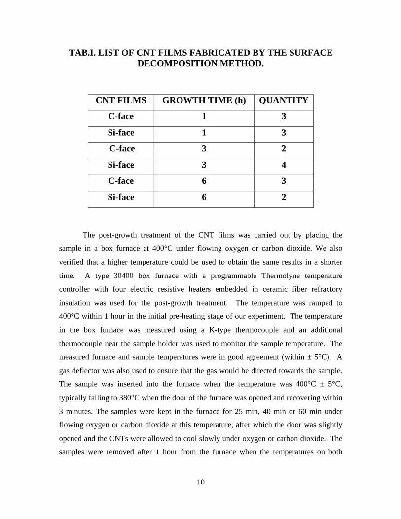
1700°C and under a pressure of 10-4 Torr are shown in Tab.I.
A typical continuous film of vertically aligned carbon nanotubes with a thickness
of 250 nm was obtained for the carbon-faced sample heated for 1 h at 1700°C. The
CNTs were both single- and multi-walled (SWNTs and MWNTs). The nanotube
diameter decreases with height and is wider at the interface between the SiC substrate and
the CNT film. Amorphous carbon and a small amount of oxygen were also detected in
the CNT films by X-ray photoelectron spectroscopy (XPS) [28]. The amorphous carbon
is the residual carbon left on the surface of the carbon nanotubes after the sublimation of
silicon from the surface of silicon carbide. As measured by Energy Despersive X-ray
Spectroscopy (EDS) on the transmission electron microscopy (TEM) samples, the
resulting CNT films contained less than 1% by weight of silicon. The CNTs formed from
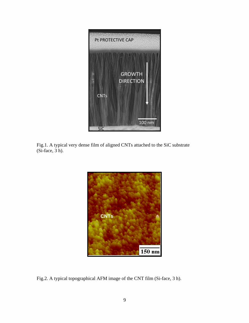
the crystalline substrate were well-aligned and straight as shown in Fig.1. This typical
cross-section transmission electron micrograph was obtained by using a Philips CM-200
field emission gun (FEG) TEM operated at 200 kV. Fig.2 shows a typical topographical
AFM image of the CNT film obtained by using the tapping mode (Veeco multimode V
AFM/SPM).
The length of the CNTs increased almost linearly with growth time at 1700°C,
reaching approximately 300 nm on the silicon face and 500 nm on the carbon face for a
6 h growth time [21]. The rate of formation of CNTs on the carbon face of the silicon
carbide substrate is 1.7 times that on the silicon face. This difference in formation rates
could be explained by differences in surface preparation and/or the presence of a thin
oxide layer on the silicon-terminated face.
9
Fig.1. A typical very dense film of aligned CNTs attached to the SiC substrate (Si-face, 3 h).
Fig.2. A typical topographical AFM image of the CNT film (Si-face, 3 h).
Pt PROTECTIVE CAP
GROWTH DIRECTION
CNTs
SiC
100 nm
CNTs
10
TAB.I. LIST OF CNT FILMS FABRICATED BY THE SURFACE DECOMPOSITION METHOD.
CNT FILMS GROWTH TIME (h) QUANTITY
C-face 1 3
Si-face 1 3
C-face 3 2
Si-face 3 4
C-face 6 3
Si-face 6 2
The post-growth treatment of the CNT films was carried out by placing the
sample in a box furnace at 400°C under flowing oxygen or carbon dioxide. We also
verified that a higher temperature could be used to obtain the same results in a shorter
time. A type 30400 box furnace with a programmable Thermolyne temperature
controller with four electric resistive heaters embedded in ceramic fiber refractory
insulation was used for the post-growth treatment. The temperature was ramped to
400°C within 1 hour in the initial pre-heating stage of our experiment. The temperature
in the box furnace was measured using a K-type thermocouple and an additional
thermocouple near the sample holder was used to monitor the sample temperature. The
measured furnace and sample temperatures were in good agreement (within ± 5°C). A
gas deflector was also used to ensure that the gas would be directed towards the sample.
The sample was inserted into the furnace when the temperature was 400°C ± 5°C,
typically falling to 380°C when the door of the furnace was opened and recovering within
3 minutes. The samples were kept in the furnace for 25 min, 40 min or 60 min under
flowing oxygen or carbon dioxide at this temperature, after which the door was slightly
opened and the CNTs were allowed to cool slowly under oxygen or carbon dioxide. The
samples were removed after 1 hour from the furnace when the temperatures on both
11
meters were 100°C and Tab.II shows the list of the samples which we were chosen for
the demonstration of the purification/uncapping procedure.
TAB.II. POST-GROWTH TREATMENT OF CNT FILMS.
CNT FILM DWELLING TIME
(min) at 400°C
OXIDATIVE TREATMENT
Si-face (3 h)
25
O2
40
60
Si-face (6 h)
25
CO2
40
60
STRUCTURAL AND CHEMICAL CHARACTERIZATION
After each step of the purification/uncapping procedure, before and after the
annealing process, our samples were subjected to structural, chemical and physical
analyses. SEM, TEM, AFM, XRD, EDS and evanescent microwave measurements were
carried out for the samples listed in Tab.II.
A Transmission Electron Microscope/Electron Diffraction Spectroscopy
(TEM/EDS) system was used to determine the percentage composition of silicon and
carbon in the SiC wafer before and after growth of the CNT to compare the change in the
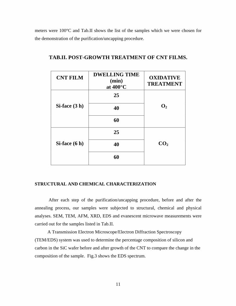
composition of the sample. Fig.3 shows the EDS spectrum.
12
Fig.3. EDS spectrum of the SiC wafer before and after the growth of the CNT.
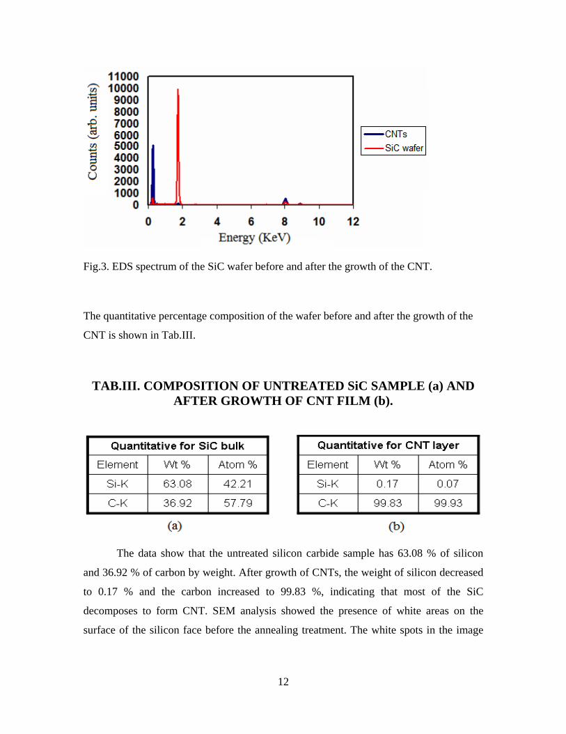
The quantitative percentage composition of the wafer before and after the growth of the
CNT is shown in Tab.III.
TAB.III. COMPOSITION OF UNTREATED SiC SAMPLE (a) AND AFTER GROWTH OF CNT FILM (b).
The data show that the untreated silicon carbide sample has 63.08 % of silicon
and 36.92 % of carbon by weight. After growth of CNTs, the weight of silicon decreased
to 0.17 % and the carbon increased to 99.83 %, indicating that most of the SiC
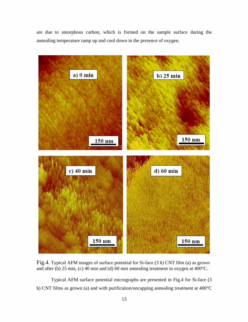
decomposes to form CNT. SEM analysis showed the presence of white areas on the
surface of the silicon face before the annealing treatment. The white spots in the image
13
are due to amorphous carbon, which is formed on the sample surface during the
annealing temperature ramp up and cool down in the presence of oxygen.
Fig.4. Typical AFM images of surface potential for Si-face (3 h) CNT film (a) as grown and after (b) 25 min, (c) 40 min and (d) 60 min annealing treatment in oxygen at 400°C. Typical AFM surface potential micrographs are presented in Fig.4 for Si-face (3
h) CNT films as grown (a) and with purification/uncapping annealing treatment at 400°C
14
after 25 min (b), 40 min (c) and 60 min (d) dwelling time. A near field evanescent
microwave microscopy sensor was used to characterize the CNT films through frequency
shift measurements. The relative sensitivity of the microscope is in the range of 10-2 and
the resolution is governed by the radius of the probe-tip [26]. The microwave probe
consists of a tuned λ/4 coaxial transmission line with an end wall aperture. A transverse
electromagnetic wave created by a frequency generator moves along the coaxial probe
and is totally internally reflected at the surface of the end wall aperture. The evanescent
waves emanate from a sharpened tip extending concentrically through the aperture and
interact with the sample. The coaxial microwave probe is capacitively coupled to the
sample, and to a network analyzer through a tuning network.
The probe can be operated in two different modes:
(1) Local complex permittivity determination by measuring the quality factor and
resonant frequency shift as the tip approaches the sample. The resonant frequency data
are produced by setting the reference resonant frequency at approximately 10 μm above
the sample surface and moving the probe tip in micrometer steps to a distance of 1 μm
from the surface. The resonant frequency shift data is best fitted by a method of images
model that produces the real and complex part of permittivity [26].
(2) X-Y scanning of material properties, with a constant separation between tip and
sample. Changes in the probe's resonant frequency, quality factor and reflection
coefficient are tracked by a Hewlett-Packard 8722ES network analyzer as the probe is
moved relative to the sample using an X-Y stage driven by optically encoded, dc and
linear actuators. The probe is frame mounted to a Z-axis linear actuator assembly and the
probe-sample separation can be set precisely.
The X-Y stage actuators, network analyzer and the data acquisition are computer
controlled with National Instruments Labview® software. The complete evanescent
microwave scanning system is mounted on a vibration-damping table.
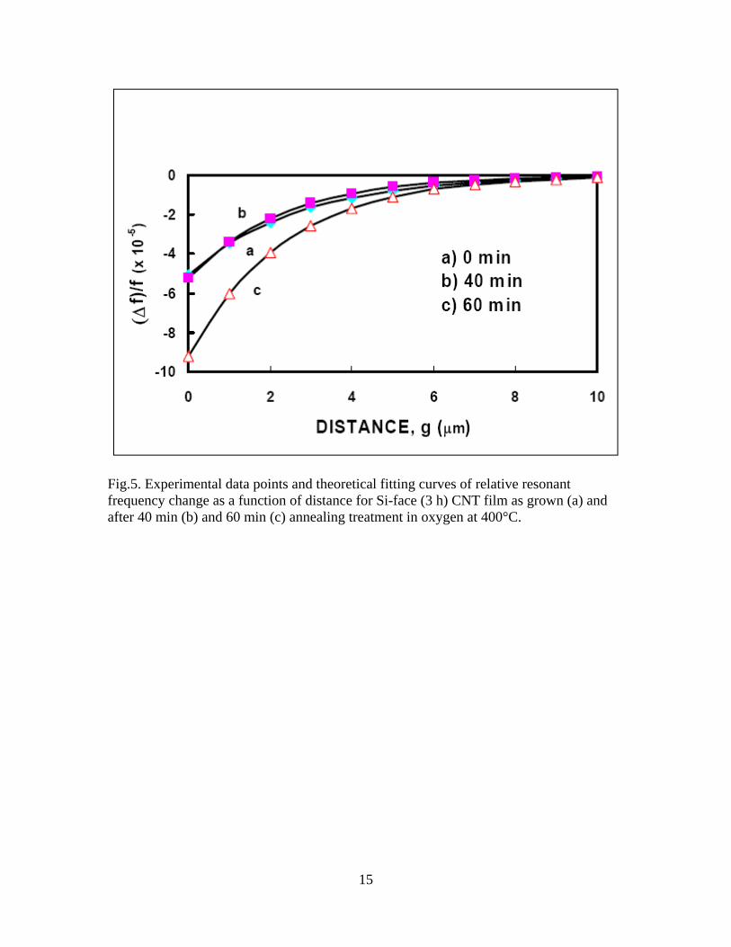
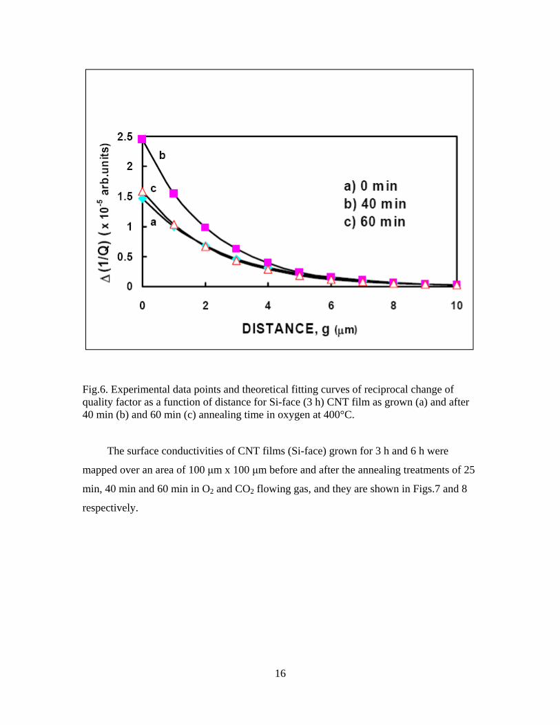
Typical experimental data for the resonant frequency and the quality factor as a
function of the tip-sample separation are plotted in Figs.5 and 6 respectively, for a CNT
film (Si-face) grown for 3 h.
15
Fig.5. Experimental data points and theoretical fitting curves of relative resonant frequency change as a function of distance for Si-face (3 h) CNT film as grown (a) and after 40 min (b) and 60 min (c) annealing treatment in oxygen at 400°C.
16
Fig.6. Experimental data points and theoretical fitting curves of reciprocal change of quality factor as a function of distance for Si-face (3 h) CNT film as grown (a) and after 40 min (b) and 60 min (c) annealing time in oxygen at 400°C.
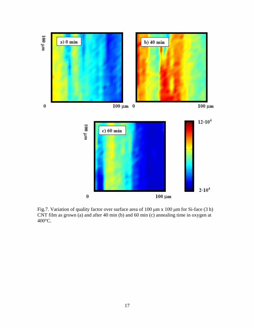
The surface conductivities of CNT films (Si-face) grown for 3 h and 6 h were
mapped over an area of 100 μm x 100 μm before and after the annealing treatments of 25
min, 40 min and 60 min in O2 and CO2 flowing gas, and they are shown in Figs.7 and 8
respectively.
17
Fig.7. Variation of quality factor over surface area of 100 μm x 100 μm for Si-face (3 h) CNT film as grown (a) and after 40 min (b) and 60 min (c) annealing time in oxygen at 400°C.
18
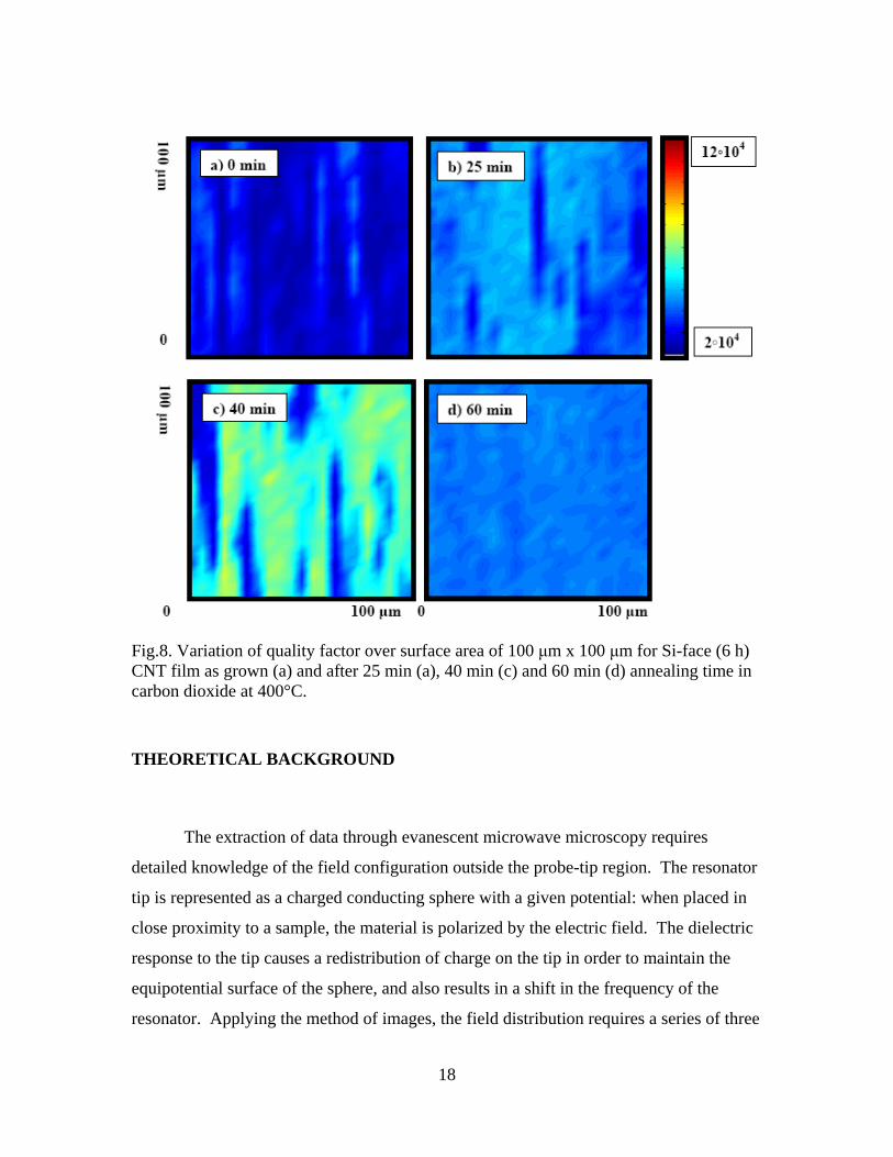
Fig.8. Variation of quality factor over surface area of 100 μm x 100 μm for Si-face (6 h) CNT film as grown (a) and after 25 min (a), 40 min (c) and 60 min (d) annealing time in carbon dioxide at 400°C.
THEORETICAL BACKGROUND
The extraction of data through evanescent microwave microscopy requires
detailed knowledge of the field configuration outside the probe-tip region. The resonator
tip is represented as a charged conducting sphere with a given potential: when placed in
close proximity to a sample, the material is polarized by the electric field. The dielectric
response to the tip causes a redistribution of charge on the tip in order to maintain the
equipotential surface of the sphere, and also results in a shift in the frequency of the
resonator. Applying the method of images, the field distribution requires a series of three
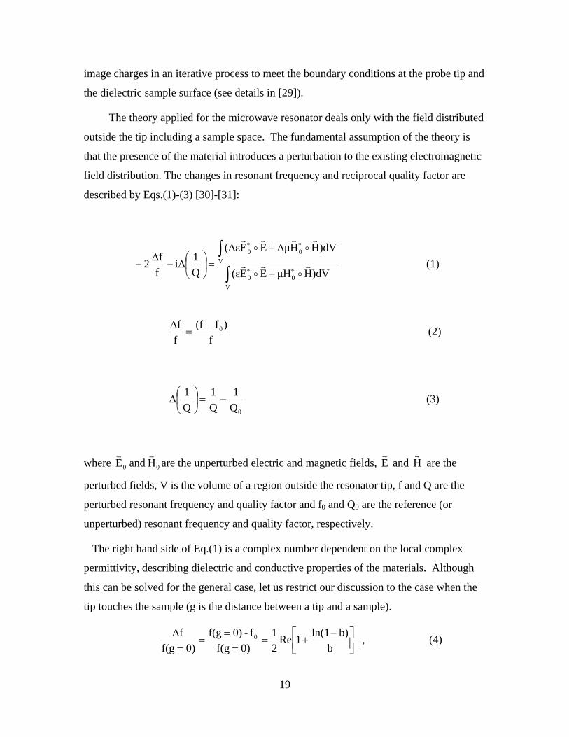
19
image charges in an iterative process to meet the boundary conditions at the probe tip and
the dielectric sample surface (see details in [29]).
The theory applied for the microwave resonator deals only with the field distributed
outside the tip including a sample space. The fundamental assumption of the theory is
that the presence of the material introduces a perturbation to the existing electromagnetic
field distribution. The changes in resonant frequency and reciprocal quality factor are
described by Eqs.(1)-(3) [30]-[31]:
V
00
V
00
)dVHμHEE(ε
)dVHHμEEε(
Q
1iΔ
f
Δf2
(1)
f
)f(f
f
Δf 0 (2)
0Q
1
Q
1
Q
1Δ
(3)
where 00 H and E
are the unperturbed electric and magnetic fields, E
and H
are the
perturbed fields, V is the volume of a region outside the resonator tip, f and Q are the
perturbed resonant frequency and quality factor and f0 and Q0 are the reference (or
unperturbed) resonant frequency and quality factor, respectively.
The right hand side of Eq.(1) is a complex number dependent on the local complex
permittivity, describing dielectric and conductive properties of the materials. Although
this can be solved for the general case, let us restrict our discussion to the case when the
tip touches the sample (g is the distance between a tip and a sample).
b
b)ln(11Re
2
1
0)f(g
f-0)f(g
0)f(g
Δf 0 , (4)
20
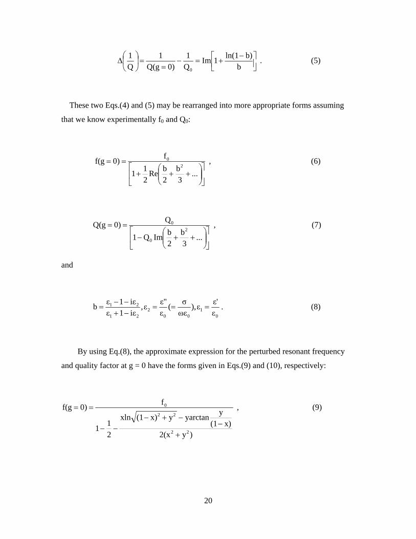
b
b)ln(11Im
Q
1
0)Q(g
1
Q
1
0
. (5)
These two Eqs.(4) and (5) may be rearranged into more appropriate forms assuming
that we know experimentally f0 and Q0:
...
3
b
2
bRe
2
11
f0)f(g
2
0 , (6)
...
3
b
2
bImQ1
Q0)Q(g
2
0
0 , (7)
and
0
100
221
21
ε
ε'ε),
ωε
σ(
ε
ε"ε,
iε1ε
iε1εb
. (8)
By using Eq.(8), the approximate expression for the perturbed resonant frequency
and quality factor at g = 0 have the forms given in Eqs.(9) and (10), respectively:
)y2(xx)(1
yyarctanyx)(1xln
2
11
f0)f(g
22
22
0
, (9)
21
22
22
0
0
yx
yx)(1ylnx)(1
yxarctan
Q1
Q0)Q(g
, (10)
where
β
2εy ,
β
αx 2 , (11)
22
21
22
21 ε1)(εβ1,εεα .
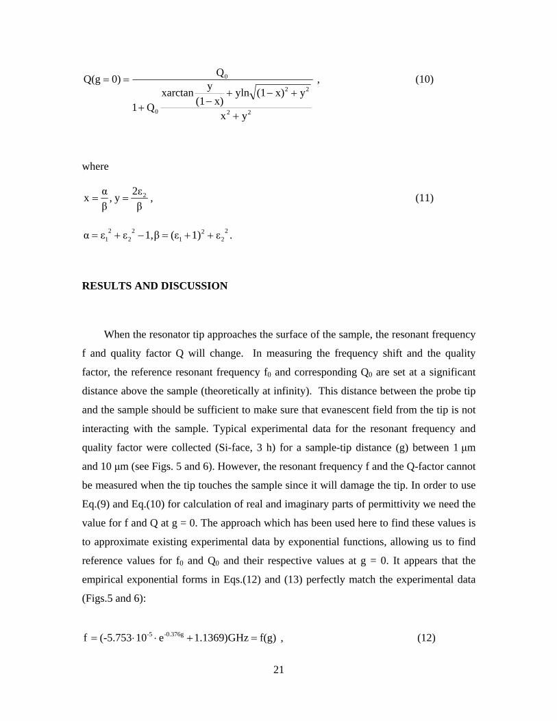
RESULTS AND DISCUSSION
When the resonator tip approaches the surface of the sample, the resonant frequency
f and quality factor Q will change. In measuring the frequency shift and the quality
factor, the reference resonant frequency f0 and corresponding Q0 are set at a significant
distance above the sample (theoretically at infinity). This distance between the probe tip
and the sample should be sufficient to make sure that evanescent field from the tip is not
interacting with the sample. Typical experimental data for the resonant frequency and
quality factor were collected (Si-face, 3 h) for a sample-tip distance (g) between 1 μm
and 10 μm (see Figs. 5 and 6). However, the resonant frequency f and the Q-factor cannot
be measured when the tip touches the sample since it will damage the tip. In order to use
Eq.(9) and Eq.(10) for calculation of real and imaginary parts of permittivity we need the
value for f and Q at g = 0. The approach which has been used here to find these values is
to approximate existing experimental data by exponential functions, allowing us to find
reference values for f0 and Q0 and their respective values at g = 0. It appears that the
empirical exponential forms in Eqs.(12) and (13) perfectly match the experimental data
(Figs.5 and 6):
f(g)GHz)1369.1e10(-5.753f -0.376g-5 , (12)
22
1/Q(g)10269.2e101.470 1/Q 5-0.388g-5 , (13)
giving the values for f and Q in Eq.(14):
.103.7390)1/Q(g
GHz, 1.13680)f(g ,102.2691/Q GHz, 1369.1f5-
-500
(14)
The changes in resonant frequency and quality factor between these two extreme
positions therefore amount to:
.10470.1Q
1
0)Q(g
1
Q
1
,10061.50)f(g
f-0)f(g
0)f(g
Δf
5
0
50
(15)
Eqs.(16) and (17) can be obtained from Eqs.(9) and (10):
)y(x
x)(1
yyarctanyx)(1xln
10)f(gA
f222
22
, (16)
22
22
yx
yx)(1ylnx)(1
yxarctan
Q
1
B
1
. (17)
Substituting the values from Eq.(15), and the values -4-5 101.738A and104.12B
determined experimentally [26], we can solve Eqs.(16) and (17) with respect to x and y.
By using Eq.(11) we finally arrive at the effective values of complex permittivity listed in
23
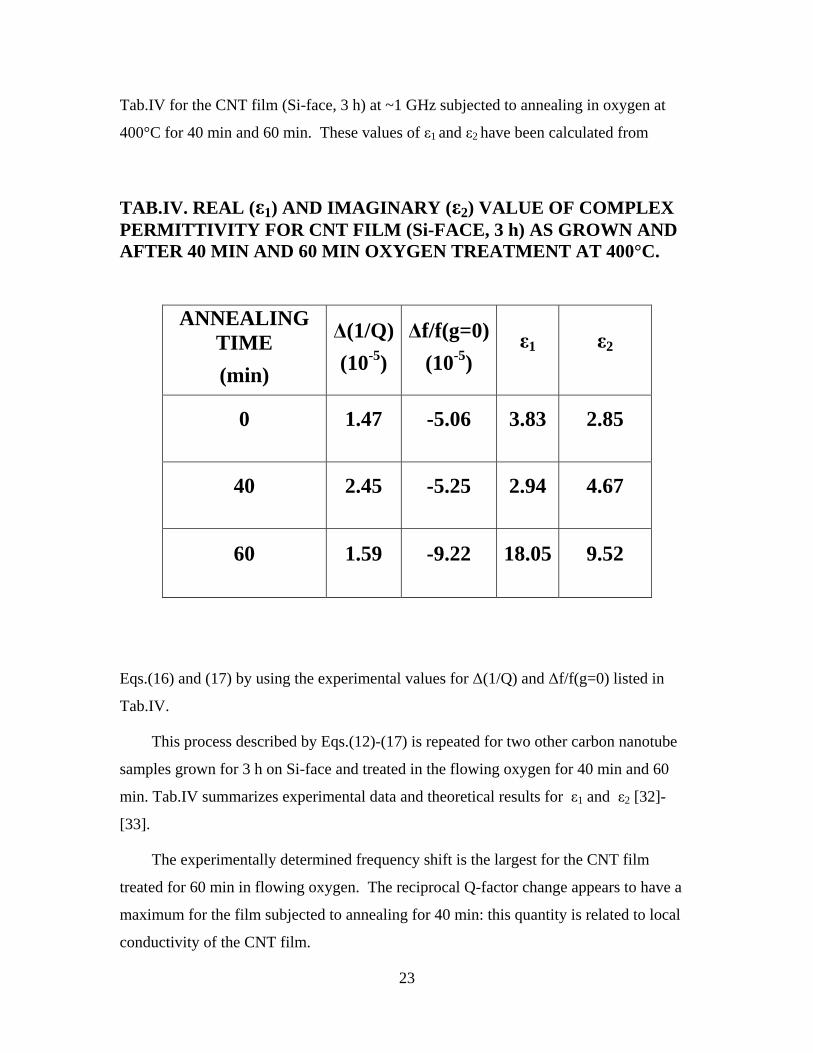
Tab.IV for the CNT film (Si-face, 3 h) at ~1 GHz subjected to annealing in oxygen at
400°C for 40 min and 60 min. These values of ε1 and ε2 have been calculated from
TAB.IV. REAL (ε1) AND IMAGINARY (ε2) VALUE OF COMPLEX PERMITTIVITY FOR CNT FILM (Si-FACE, 3 h) AS GROWN AND AFTER 40 MIN AND 60 MIN OXYGEN TREATMENT AT 400°C.
ANNEALING TIME
(min)
Δ(1/Q)
(10-5)
Δf/f(g=0)
(10-5) ε1 ε2
0 1.47 -5.06 3.83 2.85
40 2.45 -5.25 2.94 4.67
60 1.59 -9.22 18.05 9.52
Eqs.(16) and (17) by using the experimental values for Δ(1/Q) and Δf/f(g=0) listed in
Tab.IV.
This process described by Eqs.(12)-(17) is repeated for two other carbon nanotube
samples grown for 3 h on Si-face and treated in the flowing oxygen for 40 min and 60
min. Tab.IV summarizes experimental data and theoretical results for ε1 and ε2 [32]-
[33].
The experimentally determined frequency shift is the largest for the CNT film
treated for 60 min in flowing oxygen. The reciprocal Q-factor change appears to have a
maximum for the film subjected to annealing for 40 min: this quantity is related to local
conductivity of the CNT film.
24
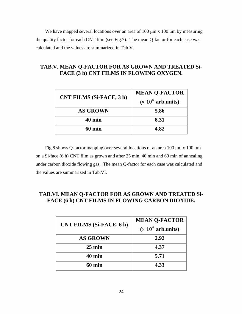
We have mapped several locations over an area of 100 μm x 100 μm by measuring
the quality factor for each CNT film (see Fig.7). The mean Q-factor for each case was
calculated and the values are summarized in Tab.V.
TAB.V. MEAN Q-FACTOR FOR AS GROWN AND TREATED Si-FACE (3 h) CNT FILMS IN FLOWING OXYGEN.
CNT FILMS (Si-FACE, 3 h) MEAN Q-FACTOR
(104 arb.units)
AS GROWN 5.86
40 min 8.31
60 min 4.82
Fig.8 shows Q-factor mapping over several locations of an area 100 μm x 100 μm
on a Si-face (6 h) CNT film as grown and after 25 min, 40 min and 60 min of annealing
under carbon dioxide flowing gas. The mean Q-factor for each case was calculated and
the values are summarized in Tab.VI.
TAB.VI. MEAN Q-FACTOR FOR AS GROWN AND TREATED Si-FACE (6 h) CNT FILMS IN FLOWING CARBON DIOXIDE.
CNT FILMS (Si-FACE, 6 h) MEAN Q-FACTOR
(104 arb.units)
AS GROWN 2.92
25 min 4.37
40 min 5.71
60 min 4.33
25
From the conductivity maps and the data recorded in the Tabs.V-VI, it is clear that
the overall surface conductivity of the sample reaches a maximum after 40 minutes of
annealing independent of the type of gas used. The mean conductivity increases 34.2%
after 25 min and 41.8 % after 40 min of annealing for the CNT film (Si-face, 3 h). This
is due to the annealing treatment which removes the amorphous carbon layer and
adsorbed molecules from the surface of carbon nanotubes. However, after 60 min of
annealing, there is a 41.9 % decrease in the conductivity. This is because, after 60 min
carbon nanotubes are already uncapped (see Fig.4) and due to oxidation of the tube tips
they start to be more dielectric, which lowers the overall conductivity of the CNT film.
The same behavior was observed in other CNT films including these treated in flowing
carbon dioxide. The percentage of change was slightly higher in the film treated with
carbon dioxide.
CONCLUSION
The surface conductivity plots show that the conductivity of the CNT films
improved after 25 min and reached a maximum after 40 min of annealing. This is
because the annealing treatment removes the amorphous carbon and the adsorbed
molecules from the surface of the CNT film. These results have been confirmed by the
AFM analysis (see Fig.4). The clean CNT films have a higher conductivity which
explains the increase in the Q-factor after the annealing treatment. However, after 60
min, the conductivity decreases as the carbon nanotubes appear to be opened and these
oxidized and open tips result in the lower conductivity of the CNT film. The shift of the
reciprocal Q-factor between g = 0 and infinity is in agreement with the experimental data
i.e., the shift in the reciprocal of the quality factor is greater for the most conductive CNT
film.
In summary, it is important to stress that CNT films fabricated by thermal
decomposition of SiC did not show significant percolative behavior based on evanescent
26
microwave measurements or spectroscopic ellipsometry [29,32]. This could be due to the
presence of amorphous carbon in the system, occupying space between carbon nanotubes
and on the surface of the CNT films and/or due to a majority of single- or multi-walled
carbon nanotubes being semiconducting. The treatment of CNT films in oxygen or in
carbon dioxide in 40 min time removes amorphous carbon at least from the film surface
causing an increase in surface conductivity. If the oxidation time is longer then 40 min
apparently the presence of open tips of nanotubes results in a decrease of the CNT film
surface conductivity. This maximum in the quality factor due to mapping (Tabs.IV-V) or
the maximum in the total change in the reciprocal of the quality factor (Fig.6) can be an
indicator of the beginning of the uncapping process of the carbon nanotubes. Depending
on the storage (uncapped CNTs) or emission (capped CNTs) application we can use this
maximum as a divider between these two applications assuming that the film is already
purified from amorphous carbon. The two-point theoretical model [29] has established
very simple relationships between the complex permittivity and both the relative resonant
frequency shift of the resonator Δf/f(g = 0) and the reciprocal change of quality factor
Δ(1/Q) which have been experimentally measured. The values of the real and imaginary
parts of the complex permittivity in CNT films are amongst the other important results
coming from the model.
REFERENCES
[1] Iijima S 1991 Nature (London) 354 56
[2] Dresselhaus M S, Dresselhaus G and Eklund P C 1996 Science of fullerenes and
carbon nanotubes Academic Press New York
[3] Wildoer J W G et al. 1998 Nature 391 59
[4] Odom T W, Huang J L, Kim P and Lieber C M 1998 Nature 391 62
[5] Falvo M R et al. 1997 Nature 389 582
[6] Dai H et al. 1996 Nature 384 147
27
[7] de Heer W A, Châtelain A and Ugarte D 1995 Science 270 1179
[8] Rinzler A G et al. 1995 Science 269 1550
[9] Collins P G and Zettl A 1996 Appl. Phys. Lett. 69 1969
[10] Bonard J M et al. 1998 Ultramicroscopy 73 7
[11] Wang Q H et al. 1997 Appl. Phys. Lett. 70 3308
[12] Kariyawasam T Field Emission of Carbon Nanotubes,
http://www.physics.uc.edu/~jarrell/COURSES/ELECTRODYNAMICS/Student_
Projects/tharanga/review.pdf
[13] Bonard J M, Salvetat J P, Stockli T, Forro L and Chatelain A 1999 Appl.Phys.A 69
245
[14] Seelaboyina R and Choi W B 2007 Recent Patent on Nanotechnology 1 238
[15] Seelaboyina R, Boddepalli S, Noh K S, Joen M H and Choi W B 2008
Nanotechnology 19 1
[16] Chen S Y, Miao H Y, Lue J T and Ouyang M S 2004 J.Phys.D:Appl.Phys. 37 273
[17] Liu Y M and Fan S S 2005 Solid State Commun. 133 131
[18] Nilsson L, Groening O, Emmenegger C, Kuettel O, Schaller E, Schlapbach L, Kind
H, Bonard J M and Kern K 2000 Appl.Phys.Lett. 76 2071
[19] Kusunoki M, Suzuki T, Kaneko K and Itos M 1999 Phil. Mag. Lett. 79 153
[20] Kusunoki M, Suzuki T, Hirayama T and Shibata N 2000 Appl.Phys.Lett. 77 531
[21] Mitchel W C, Boeckl J J, Toln D, Lu W, Rigueur J and Reynolds J 2005 Quantum
sensing and nanophotonic devices II, Proceedings of the SPIE 5732 77
[22] Ajayan P M, Ebbesen T W, Ichihashi T, Iijima S, Tanigaki K and Hiura H 1993
Nature 362 522
[23] Tsang S C, Harris P J F and Green M L H 1993 Nature 362 520
[24] Biro L P, Bernardo C A, Tibbetts G G and Lambin Ph Carbon Filaments and
Nanotubes: Common Origins, Differing Applications? Springer Verlag 2001, Series E:
Applied Sciences 372
28
[25] Geng H Z, Zhang X B, Mao S H, Kleinhammes A, Shimoda H, Wu Y and Zhou O
2004 Chem.Phys.Lett. 399 109
[26] Kleismit R A, ElAshry M, Kozlowski G, Amer M S, Kazimierczuk M K and
Biggers R R 2005 Supercond.Sci.Technol. 18 1197
[27] Xiang X D and Gao C 2002 Mater.Character. 48 117
[28] Boeckl J J, Mitchel W C, Rigeur J and Lu W 2005 Proceedings of International
Conference on SiC and Related Materials 1579
[29] Kozlowski G, Kleismit R A, Boeckl J J, Campbell A L, Munbodh K, Hopkins S C,
Koziol K K and Peterson T L 2008 Nanotechnology
[30] Li D Q, Free C E, Pitt K E G and Barnwell P G 2001 IEEE Microwave and Wireless
Components Lett. 11 118
[31] Sucher M and Fox J 1963 Handbook of Microwave Measurements Brooklyn NY
Brooklyn Polytechnic Inst. Press, Vol.II
[32] Harrison J, Sambandam S N, Boeckl J J, Mitchel W C, Collins W E and Lu W J
2007 J.Appl.Phys. 101 104311
[33] Fagan J A, Simpson J R, Landi B J, Richter L J, Mandelbaum I, Bajpai V, Ho D L,
Raffaelle R., Hight Walker A R, Bauer B J and Hobbie E K 2007 Phys.Rev.Lett. 98
147402-1