Embed Size (px)
DESCRIPTION
f
Citation preview
Programmable Logic Devices
ZEIT3219 Programmable Digital Systems 6-1
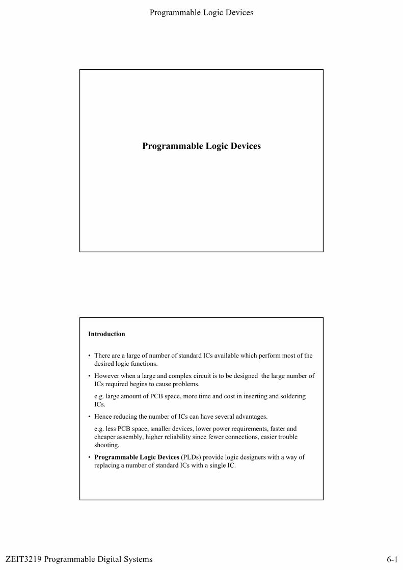
Programmable Logic Devices
Introduction
• There are a large of number of standard ICs available which perform most of the desired logic functions.
• However when a large and complex circuit is to be designed the large number of g p g gICs required begins to cause problems.
e.g. large amount of PCB space, more time and cost in inserting and soldering ICs.
• Hence reducing the number of ICs can have several advantages.
e.g. less PCB space, smaller devices, lower power requirements, faster and cheaper assembly, higher reliability since fewer connections, easier trouble p y, g y ,shooting.
• Programmable Logic Devices (PLDs) provide logic designers with a way of replacing a number of standard ICs with a single IC.
Programmable Logic Devices
ZEIT3219 Programmable Digital Systems 6-2
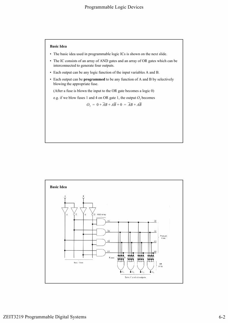
Basic Idea
• The basic idea used in programmable logic ICs is shown on the next slide.
• The IC consists of an array of AND gates and an array of OR gates which can be interconnected to generate four outputs.
• Each output can be any logic function of the input variables A and B.p y g p
• Each output can be programmed to be any function of A and B by selectively blowing the appropriate fuse.
(After a fuse is blown the input to the OR gate becomes a logic 0)
e.g. if we blow fuses 1 and 4 on OR gate 1, the output O1 becomes
O1 = 0 + AB + AB + 0 = AB + AB
Basic Idea
Programmable Logic Devices
ZEIT3219 Programmable Digital Systems 6-3
Exercise 1
What fuses would have to be blown to program the logic function O2 = A + B ?
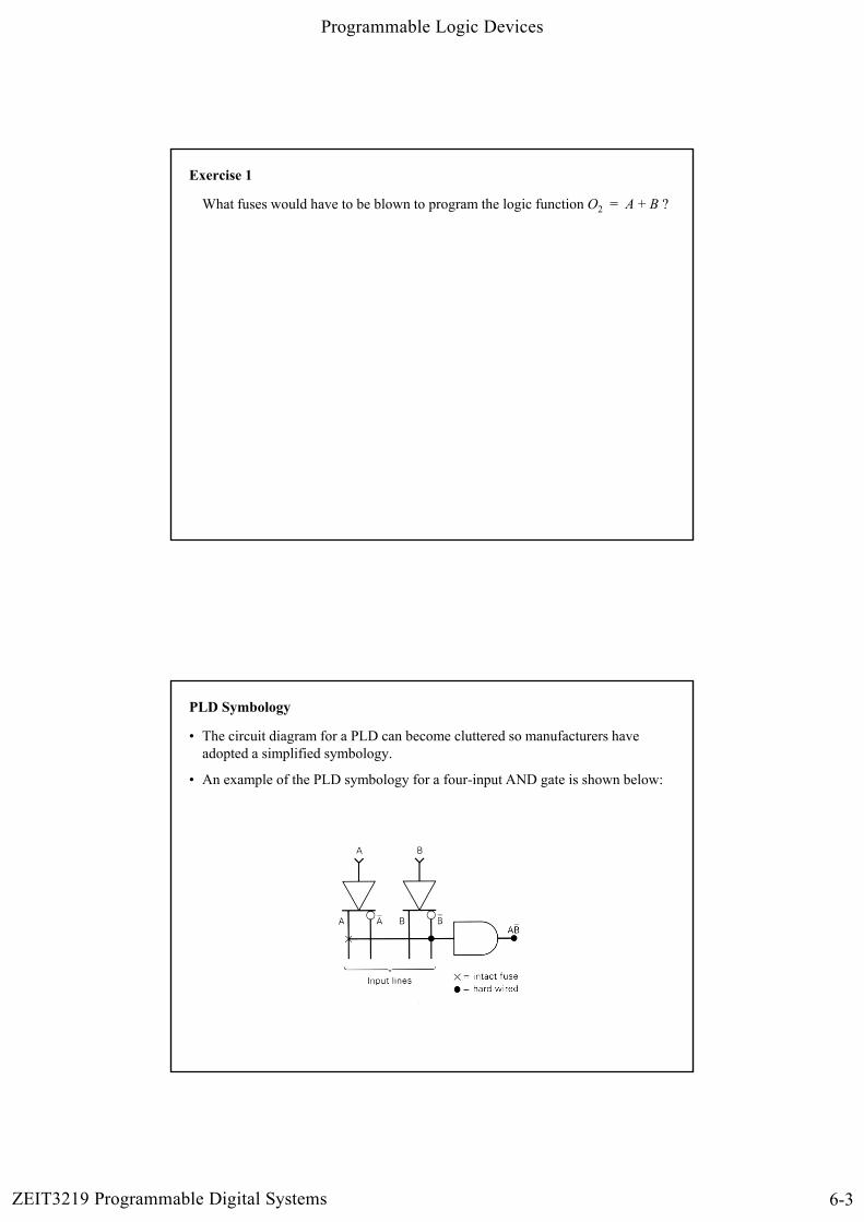
PLD Symbology
• The circuit diagram for a PLD can become cluttered so manufacturers have adopted a simplified symbology.
• An example of the PLD symbology for a four-input AND gate is shown below:
Programmable Logic Devices
ZEIT3219 Programmable Digital Systems 6-4
PLD Symbology
• The input buffers are represented as a single buffer with two outputs.
• A single line going into the AND gate is used to represent the four inputs.
• The connections from the input variable lines to the AND gate are indicated with either a cross or a dot.
• A cross indicates an intact fuse.
• A dot indicates a hard-wired connection.
• It is important to realize that the AND gate has four different inputs even though only a single line is shown.
• The actual inputs which are connected to the AND gate are shown with either a d tcross or a dot.
Exercise 2
Redraw the diagram on the previous slide to show the intact fuses required to produce the logic expression AB at the output of the AND gate.
Programmable Logic Devices
ZEIT3219 Programmable Digital Systems 6-5
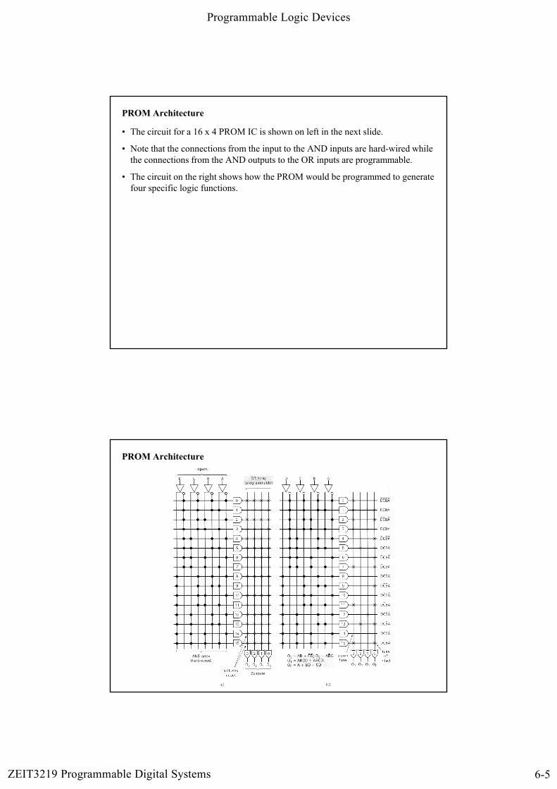
PROM Architecture
• The circuit for a 16 x 4 PROM IC is shown on left in the next slide.
• Note that the connections from the input to the AND inputs are hard-wired while the connections from the AND outputs to the OR inputs are programmable.
• The circuit on the right shows how the PROM would be programmed to generate g p g gfour specific logic functions.
PROM Architecture
Programmable Logic Devices
ZEIT3219 Programmable Digital Systems 6-6
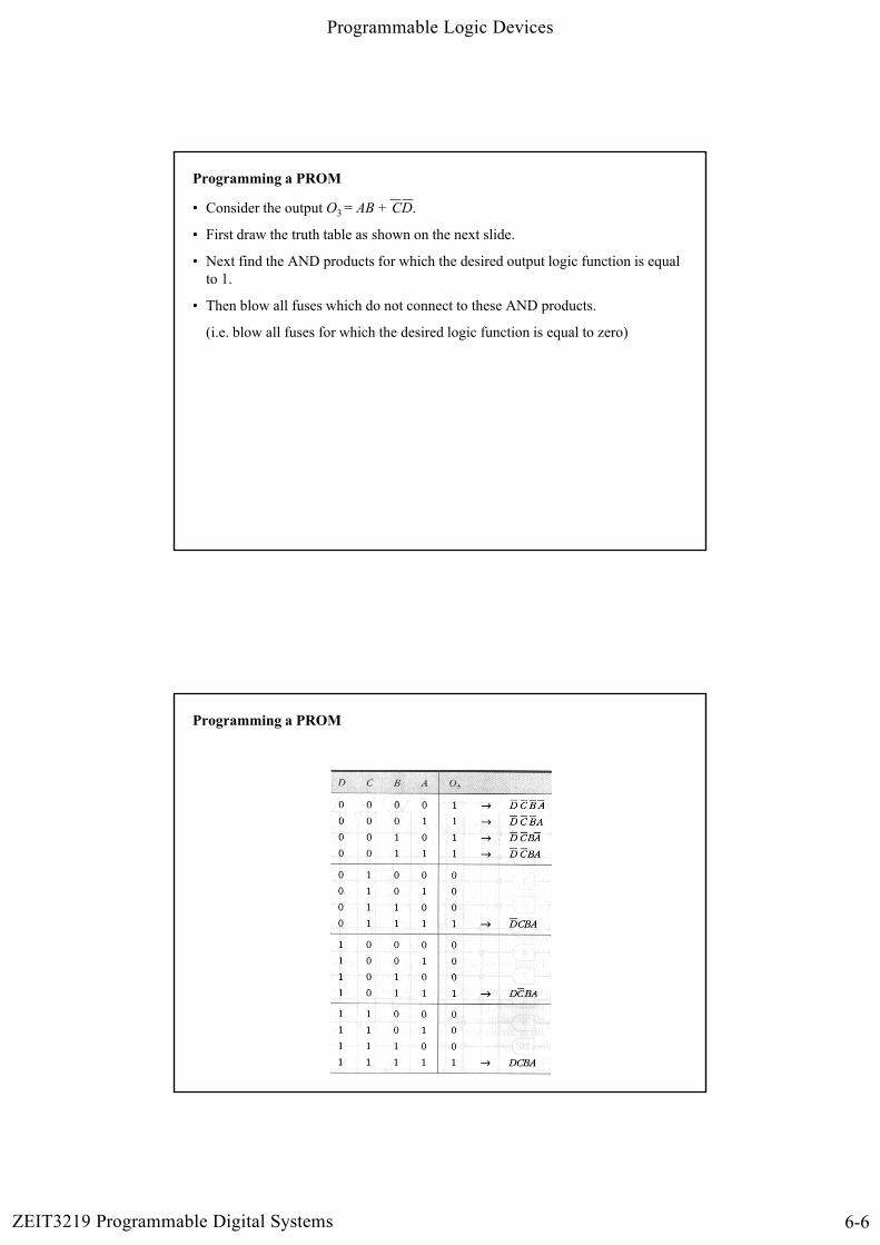
Programming a PROM
• Consider the output O3 = AB + CD.
• First draw the truth table as shown on the next slide.
• Next find the AND products for which the desired output logic function is equal to 1.
• Then blow all fuses which do not connect to these AND products.
(i.e. blow all fuses for which the desired logic function is equal to zero)
Programming a PROM
Programmable Logic Devices
ZEIT3219 Programmable Digital Systems 6-7
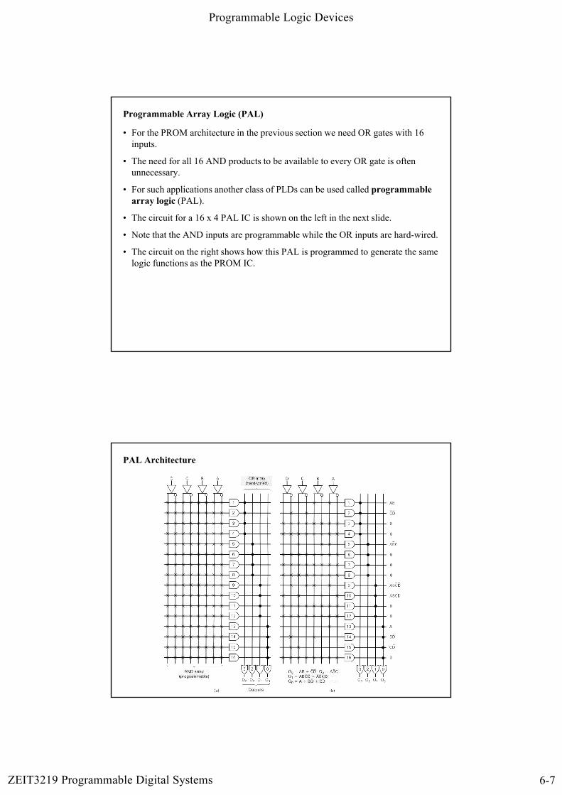
Programmable Array Logic (PAL)
• For the PROM architecture in the previous section we need OR gates with 16 inputs.
• The need for all 16 AND products to be available to every OR gate is often unnecessary.
• For such applications another class of PLDs can be used called programmable array logic (PAL).
• The circuit for a 16 x 4 PAL IC is shown on the left in the next slide.
• Note that the AND inputs are programmable while the OR inputs are hard-wired.
• The circuit on the right shows how this PAL is programmed to generate the same logic functions as the PROM IC.g
PAL Architecture

Programmable Logic Devices
ZEIT3219 Programmable Digital Systems 6-8
Programming a PAL
• The logic functions at the output of the PAL are limited to the sum of four product terms since each OR input is connected to only four AND outputs.
• So for the logic function O3 = AB + CD we rewrite this as the sum of four product terms
O3 = AB + CD + 0 + 0
• Then we program AND gates 1, 2, 3 and 4 to provide these four product terms.
• The first term is obtained by leaving the fuses which connect inputs A and B to input 1 and blowing all the rest.
• Any product outputs which are 0 can be produced by leaving all fuses intact since AABBCCDD = 0.
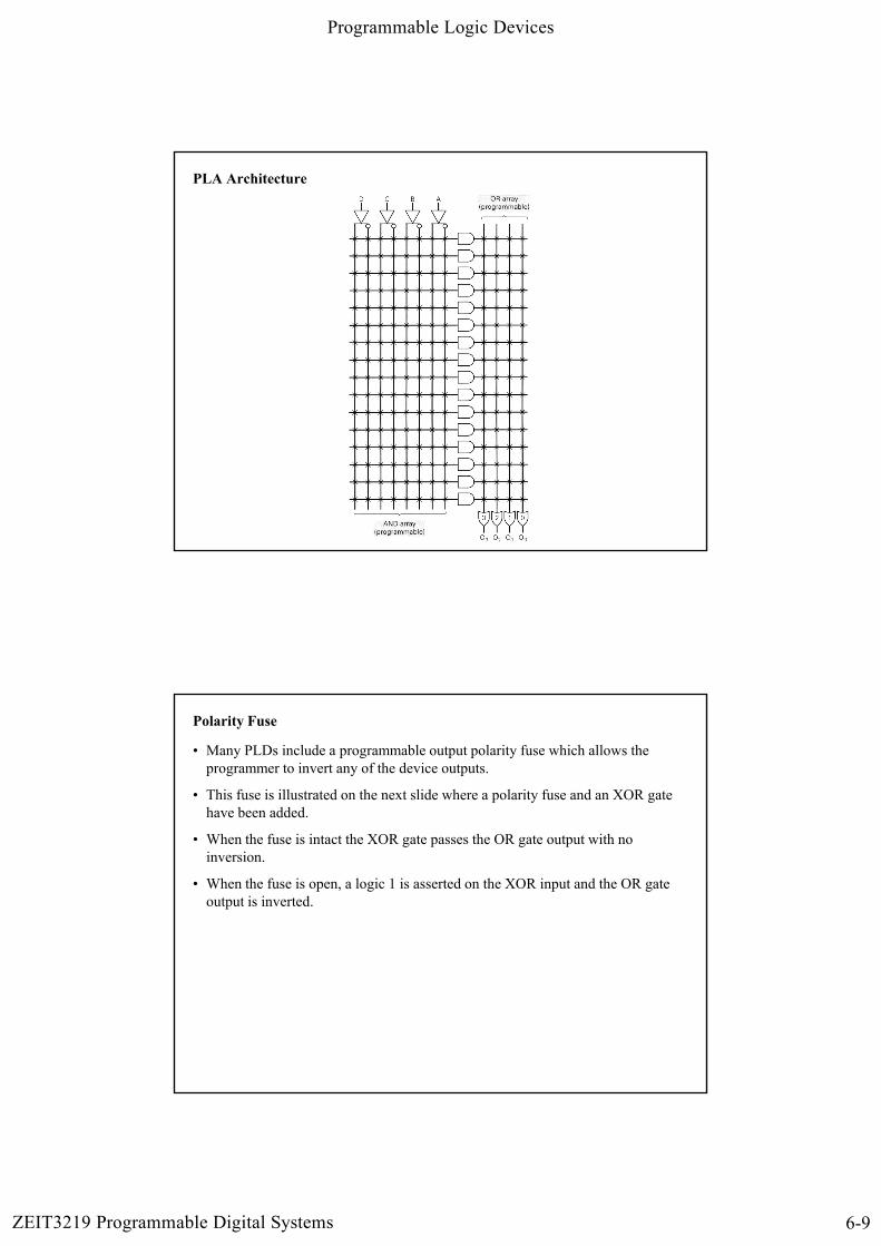
Programmable Logic Array (PLA)
• A programmable logic array (PLA) combines the characteristics of the PROM and the PAL by providing both a programmable OR array and a programmable AND array.
• The architecture of a PLA is shown on the next slide.
• A PLA is more versatile than a PROM or PAL but because it has two sets of fuses it is more difficult to manufacture, program and test.
Programmable Logic Devices
ZEIT3219 Programmable Digital Systems 6-9
PLA Architecture
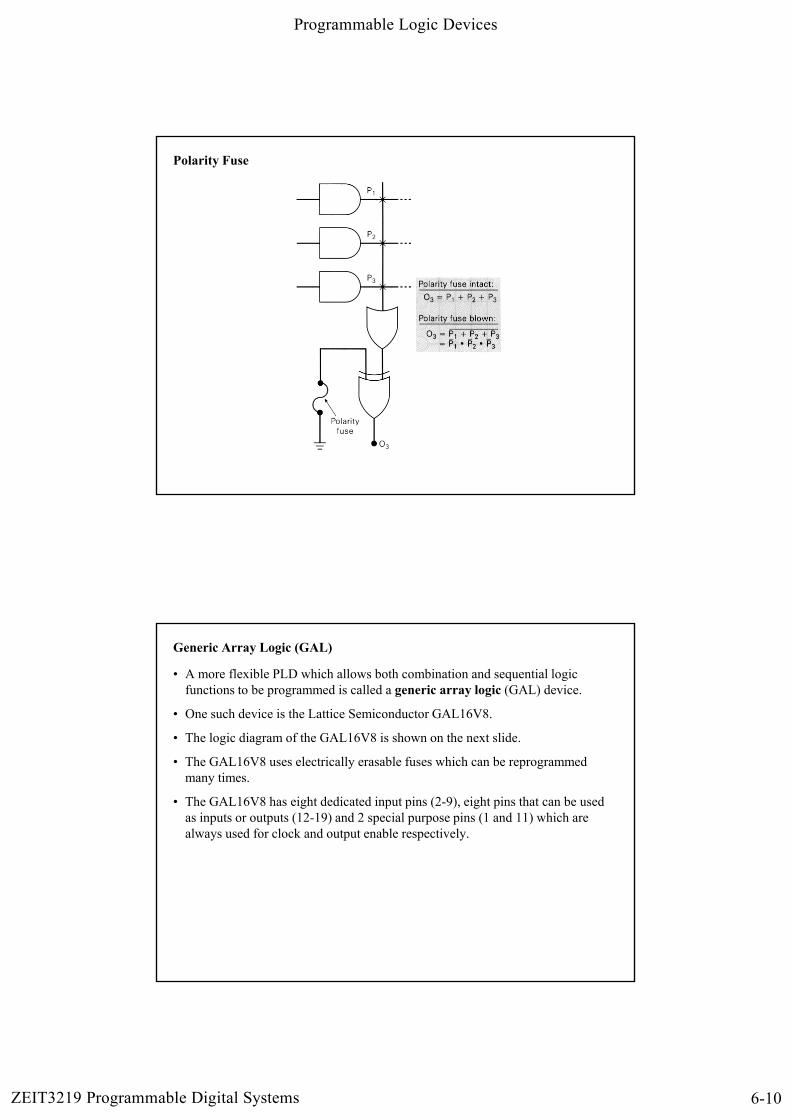
Polarity Fuse
• Many PLDs include a programmable output polarity fuse which allows the programmer to invert any of the device outputs.
• This fuse is illustrated on the next slide where a polarity fuse and an XOR gate have been added.
• When the fuse is intact the XOR gate passes the OR gate output with no inversion.
• When the fuse is open, a logic 1 is asserted on the XOR input and the OR gate output is inverted.
Programmable Logic Devices
ZEIT3219 Programmable Digital Systems 6-10
Polarity Fuse
Generic Array Logic (GAL)
• A more flexible PLD which allows both combination and sequential logic functions to be programmed is called a generic array logic (GAL) device.
• One such device is the Lattice Semiconductor GAL16V8.
• The logic diagram of the GAL16V8 is shown on the next slide. g g
• The GAL16V8 uses electrically erasable fuses which can be reprogrammed many times.
• The GAL16V8 has eight dedicated input pins (2-9), eight pins that can be used as inputs or outputs (12-19) and 2 special purpose pins (1 and 11) which are always used for clock and output enable respectively.
Programmable Logic Devices
ZEIT3219 Programmable Digital Systems 6-11
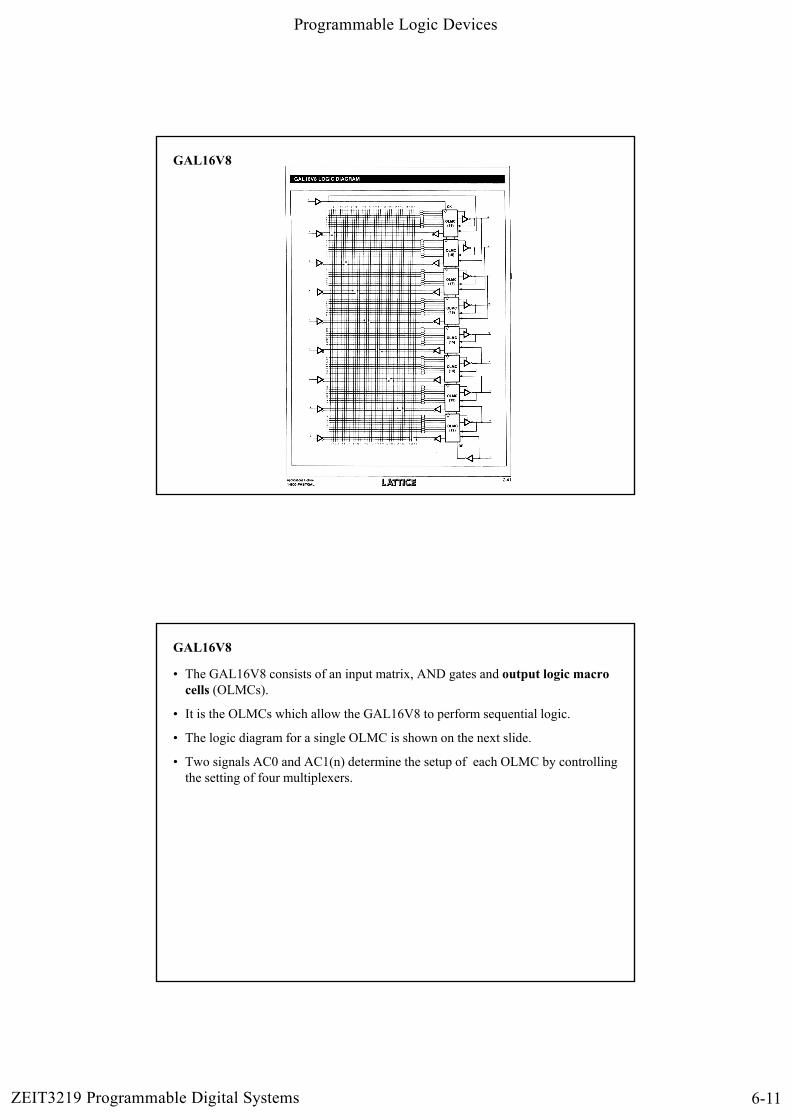
GAL16V8
GAL16V8
• The GAL16V8 consists of an input matrix, AND gates and output logic macro cells (OLMCs).
• It is the OLMCs which allow the GAL16V8 to perform sequential logic.
• The logic diagram for a single OLMC is shown on the next slide.g g g
• Two signals AC0 and AC1(n) determine the setup of each OLMC by controlling the setting of four multiplexers.
Programmable Logic Devices
ZEIT3219 Programmable Digital Systems 6-12
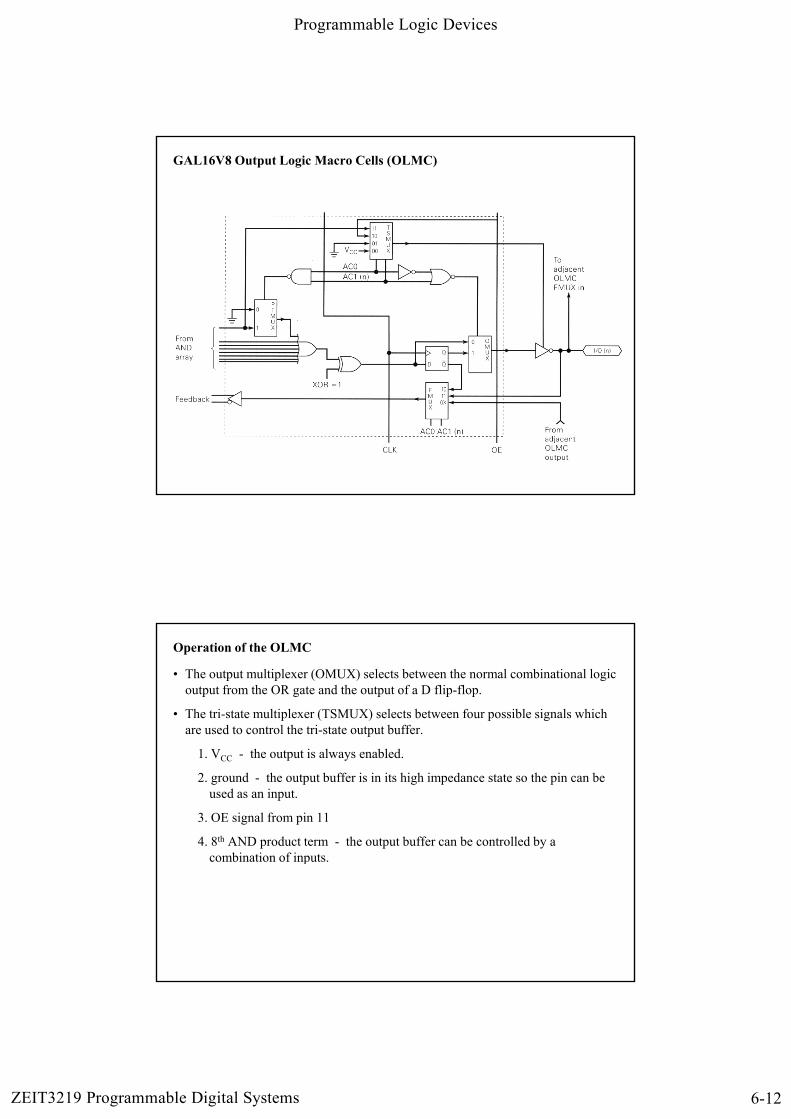
GAL16V8 Output Logic Macro Cells (OLMC)
Operation of the OLMC
• The output multiplexer (OMUX) selects between the normal combinational logic output from the OR gate and the output of a D flip-flop.
• The tri-state multiplexer (TSMUX) selects between four possible signals which are used to control the tri-state output buffer.
1. VCC - the output is always enabled.
2. ground - the output buffer is in its high impedance state so the pin can be used as an input.
3. OE signal from pin 11
4. 8th AND product term - the output buffer can be controlled by a combination of inputs.p
Programmable Logic Devices
ZEIT3219 Programmable Digital Systems 6-13
Operation of the OLMC
• The product term multiplexer (PTMUX) selects between the eighth product term and ground for the 8th input to the OR gate.
• The feedback multiplexer (FMUX) selects which signal is to be fed back to the input matrix.
• By allowing the output of the D flip-flop to be fed back to the input matrix the GAL16V8 is able to implement sequential logic functions.
Field Programmable Gate Arrays (FPGAs)
• Fills the gap between PLDs and Application Specific ICs (ASICs)
• PLDs
– limited complexity, thousands of gates
h t d i bl– cheap, easy to design, reprogrammable
• ASICS
– large complex functions, millions of gates
– customised for extremes of speed, low power, radiation hard
– (very) expensive (in small quantities) > $1 million mask set
( ) h d t d i– (very) hard to design
– long design cycles
– mistakes not detected at design time have large impact on development time and cost
Programmable Logic Devices
ZEIT3219 Programmable Digital Systems 6-14
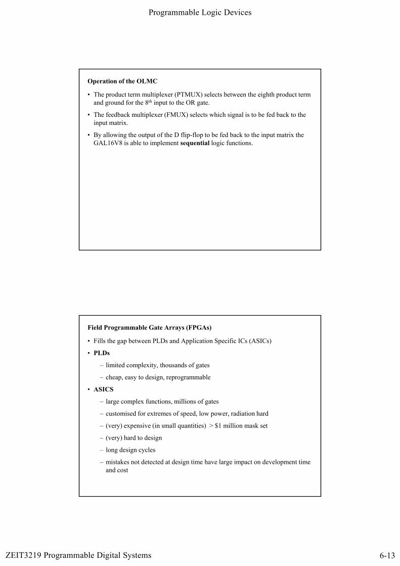
What are Field Programmable Gate Arrays (FPGAs)?
• Simple programmable logic blocks
• Massive fabric of programmable interconnects
• Large number of logic block ‘islands’ (1,000 … 100,000+) in a ‘sea’ of interconnects.
Advantages of FPGAs over ASICs
• FPGAs are perfect for rapid prototyping of digital circuits
• Easy upgrades as is the case with software
• Small development overhead
Q i k ti t k t• Quick time to market
• No minimum quantity order
• Reprogrammable
• Unique applications
– reconfigurable computing
Programmable Logic Devices
ZEIT3219 Programmable Digital Systems 6-15
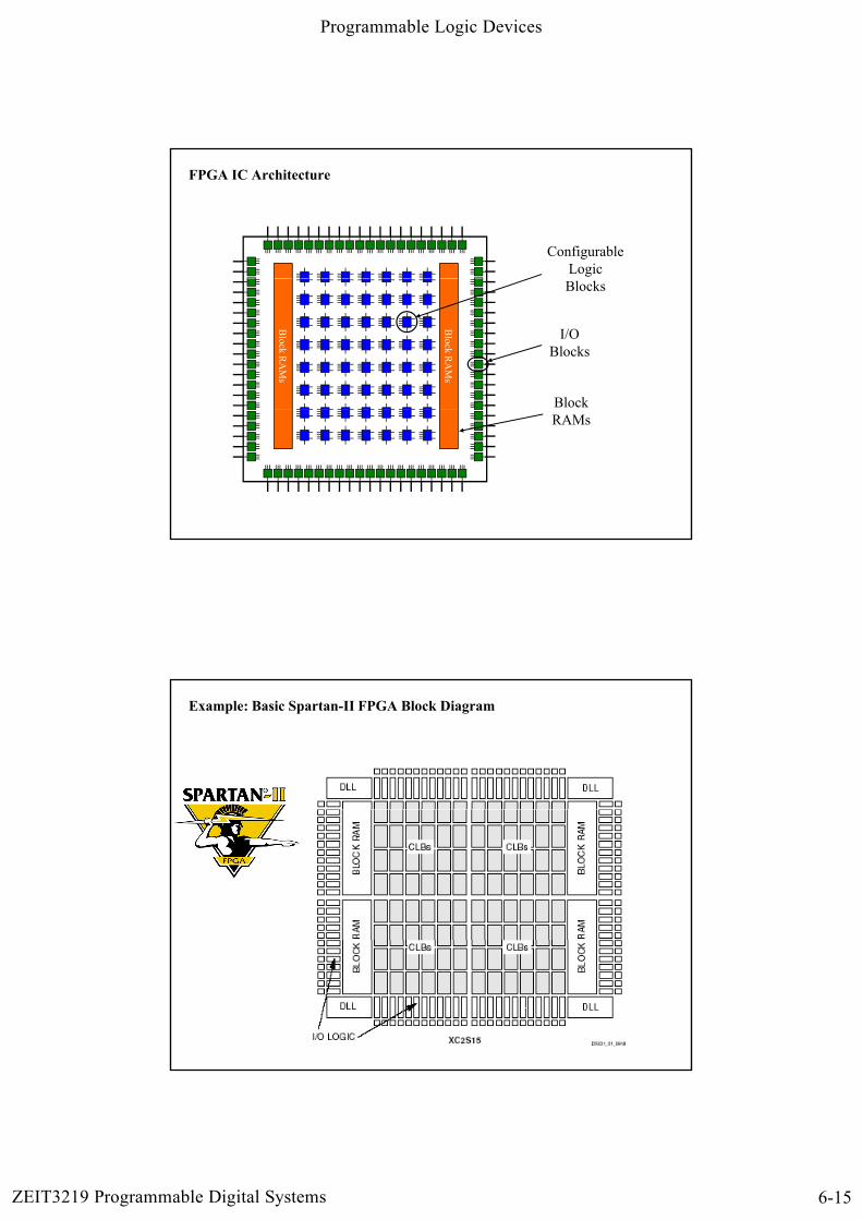
FPGA IC Architecture
ConfigurableLogic
Block R
AM
s
Block R
AM
s
Blocks
I/OBlocks
BlockRAMs
Example: Basic Spartan-II FPGA Block Diagram
Programmable Logic Devices
ZEIT3219 Programmable Digital Systems 6-16
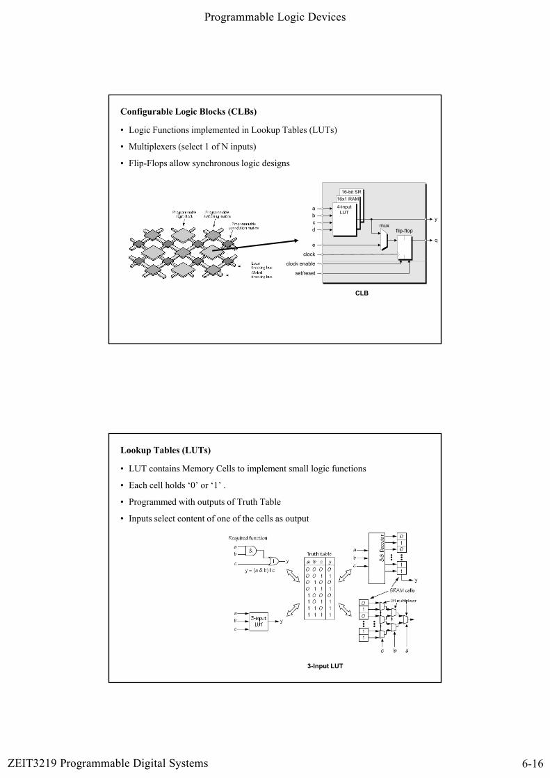
Configurable Logic Blocks (CLBs)
• Logic Functions implemented in Lookup Tables (LUTs)
• Multiplexers (select 1 of N inputs)
• Flip-Flops allow synchronous logic designs
16-bit SR
flip-flop
clock
muxy
qe
abcd
16x1 RAM
4-inputLUT
clock enable
set/reset
CLB
Lookup Tables (LUTs)
• LUT contains Memory Cells to implement small logic functions
• Each cell holds ‘0’ or ‘1’ .
• Programmed with outputs of Truth Table
I t l t t t f f th ll t t• Inputs select content of one of the cells as output
3-Input LUT
c ab
Programmable Logic Devices
ZEIT3219 Programmable Digital Systems 6-17
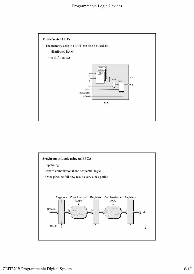
Multi-faceted LUTs
• The memory cells in a LUT can also be used as:
– distributed RAM
– a shift-register
16-bit SR
flip-flop
clock
muxy
qe
abcd
16x1 RAM
4-inputLUT
clock enable
set/reset
CLB
Synchronous Logic using an FPGA
• Pipelining
• Mix of combinational and sequential logic
• Once pipeline full new result every clock period
Data In
Registers Registers RegistersCombinationalLogic
CombinationalLogic
Clock
etc.
Programmable Logic Devices
ZEIT3219 Programmable Digital Systems 6-18
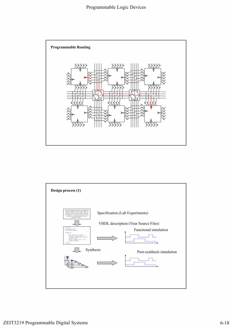
Programmable Routing
Design process (1)
Design and implement a simple unit permitting to speed up encryption with RC5-similar cipher with fixed key set on 8031 microcontroller. Unlike in
the experiment 5, this time your unit has to be able to perform an encryption algorithm by itself,
executing 32 rounds…..
Specification (Lab Experiments)
Library IEEE;use ieee.std_logic_1164.all;use ieee.std_logic_unsigned.all;
entity RC5_core isport(
clock, reset, encr_decr: in std_logic;data_input: in std_logic_vector(31 downto 0);data_output: out std_logic_vector(31 downto 0);out_full: in std_logic;key_input: in std_logic_vector(31 downto 0);key_read: out std_logic;
);end AES_core;
VHDL description (Your Source Files)
Functional simulation
Post-synthesis simulationSynthesis y
Programmable Logic Devices
ZEIT3219 Programmable Digital Systems 6-19
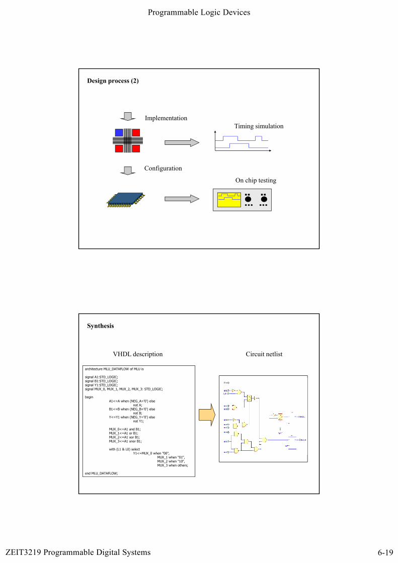
Design process (2)
ImplementationTiming simulation
Configuration
g
On chip testing
architecture MLU_DATAFLOW of MLU is
VHDL description Circuit netlist
Synthesis
signal A1:STD_LOGIC;signal B1:STD_LOGIC;signal Y1:STD_LOGIC;signal MUX_0, MUX_1, MUX_2, MUX_3: STD_LOGIC;
beginA1<=A when (NEG_A='0') else
not A;B1<=B when (NEG_B='0') else
not B;Y<=Y1 when (NEG_Y='0') else
not Y1;
MUX_0<=A1 and B1;MUX 1<=A1 or B1;MUX_1< A1 or B1;MUX_2<=A1 xor B1;MUX_3<=A1 xnor B1;
with (L1 & L0) selectY1<=MUX_0 when "00",
MUX_1 when "01",MUX_2 when "10",MUX_3 when others;
end MLU_DATAFLOW;
Programmable Logic Devices
ZEIT3219 Programmable Digital Systems 6-20
Features of synthesis tools
• Interpret Register Transfer Level (RTL) code
• Produce synthesized circuit netlist in a standard Electronic Design Interchange Format (EDIF) file
• Give preliminary performance estimatesp y p
• Some can display circuit schematics corresponding to EDIF netlist
Implementation
• After synthesis the entire implementation process is performed by FPGA vendor tools, e.g.:
– Xilinx
– Altera
Programmable Logic Devices
ZEIT3219 Programmable Digital Systems 6-21
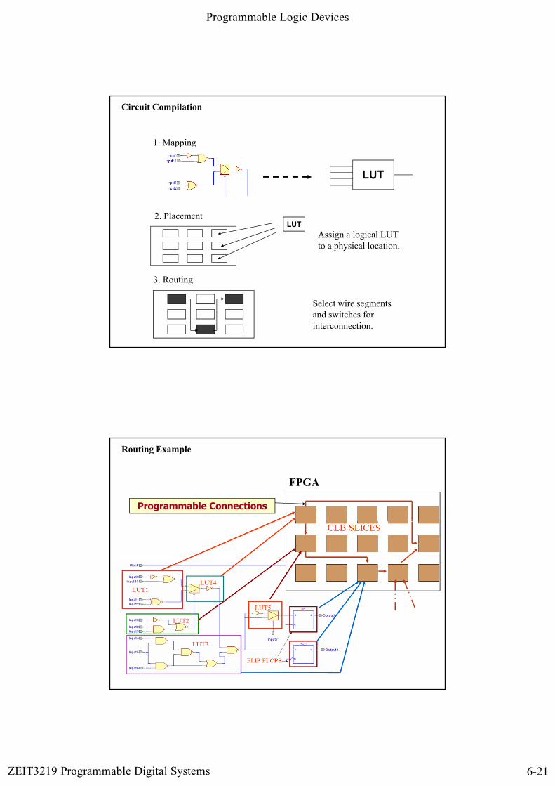
Circuit Compilation
LUT
1. Mapping
LUT
Assign a logical LUT to a physical location.
2. Placement
Select wire segmentsand switches forinterconnection.
3. Routing
Routing Example
Programmable Connections
FPGA

Programmable Logic Devices
ZEIT3219 Programmable Digital Systems 6-22
Programmable Logic Devices