Embed Size (px)
Citation preview
1
1
LOGIC DEVICES
Unit Structure
1.1 Introduction
1.2 Tristate devices
1.3 Buffers
1.4 Encoder
1.5 Decoder
1.6 Latches
1.7 Summary
1.8 Review Questions
1.9 Reference
1.0 OBJECTIVES
After studying this chapter you should be able to Understand the working of tri state devices Explain the use of buffer in electronics Describe the use of encoder and decoder in 8085 Understand the working of Latch
1.1 INTRODUCTION
The chapter reviews logic theory of encoder and decoder. It
discusses the working of tristate devices and latch. These logic devices play an important role in 8085 microprocessor. In order to separate the low order address bus and data bus, latch IC is used.
1.2 TRI-STATE DEVICES
Tri-state logic devices have three states:
1) Logic 1 or Low 2) Logic 0 or High 3) High impedance
A tri-state logic device has a extra input line called Enable. When this line is active (Enabled), a tri-state device functions in the same way as ordinary logic devices. When this line is not active(disabled), the logic device goes into a high impedance state,
2
as if it is disconnected from the system and practically no current is drawn from the system.
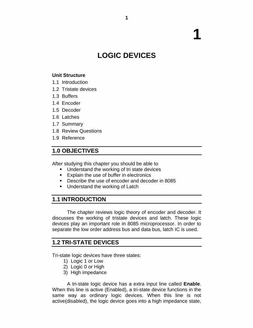
1.3 BUFFER
A Digital Buffer is a single input device that does not invert
or perform any type of logical operation on its input signal. In other words, the logic level of the output is same as that of the input. The buffer is a logic circuit that amplifies the current or power. The buffer is used primarily to increase the driving capability of a logic circuit. It is also known as driver.
Symbol Truth Table
A Tri-state Buffer
A Q
0 0
1 1
Boolean Expression Q = A Read as A gives Q
1.3.1 Tri-state Buffer
A Tri-state Buffer can be thought of as an input controlled switch which has an output that can be electronically turned "ON" or "OFF" by means of an external "Enable" signal input. This Enable signal can be either a logic "0" or a logic "1" type signal. When Enable line is low (logic „0‟), the circuit functions as a buffer. When Enable line is high (logic „1‟), its output produces an open circuit condition that is neither "High" nor "low", but instead gives an output state of very high impedance, high-Z, or more commonly Hi-Z.
Then this type of device has two logic state inputs, "0" or a "1"
but can produce three different output states, "0", "1" or "Hi-Z" which is why it is called a "3-state" device.
There are two different types of Tri-state Buffer, one whose
output is controlled by an "Active-HIGH" Enable signal and the other which is controlled by an "Active-LOW" Enable signal, as shown below
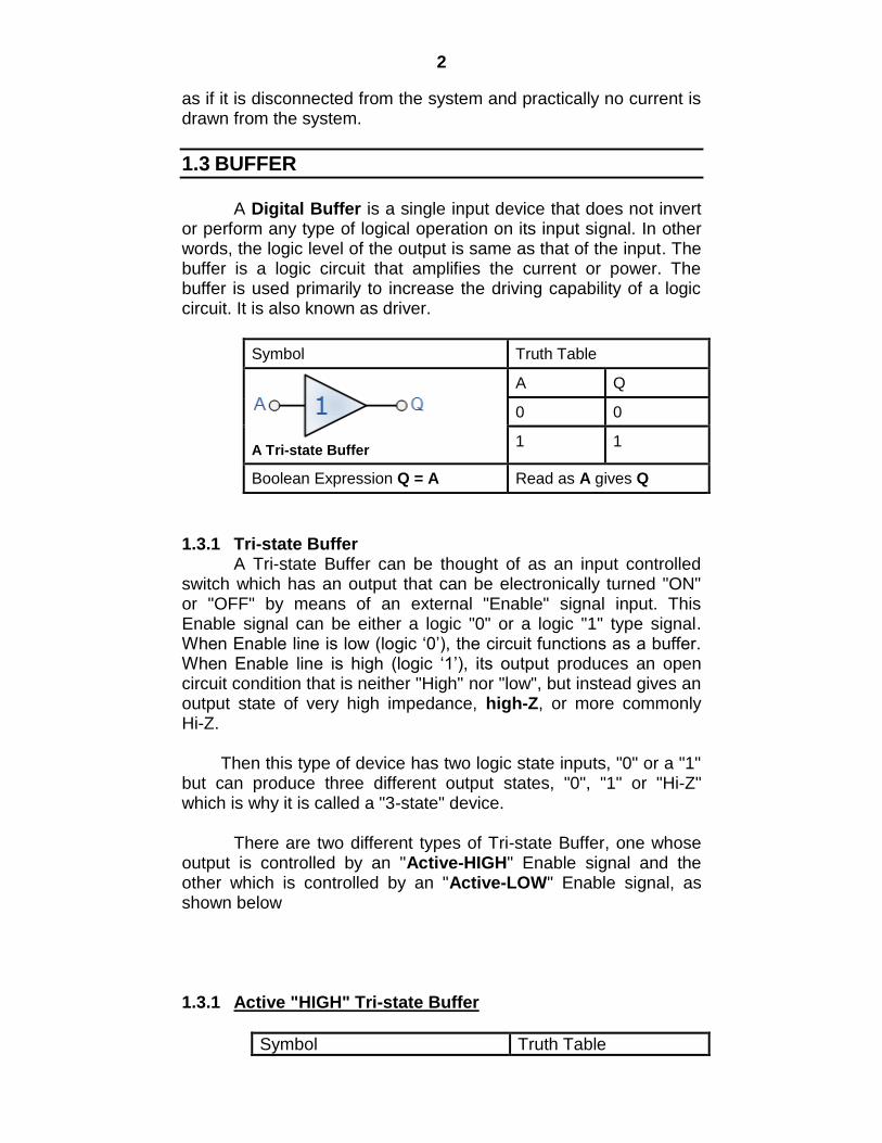
1.3.1 Active "HIGH" Tri-state Buffer
Symbol Truth Table
3
Tri-state Buffer
Enable A Q
1 0 0
1 1 1
0 0 Hi-Z
0 1 Hi-Z
Read as Output = Input if Enable is equal to "1"
An Active-high Tri-state Buffer is activated when a logic
level "1" is applied to its "enable" control line and the data passes through from its input to its output. When the enable control line is at logic level "0", the buffer output is disabled and a high impedance condition, Hi-Z is present on the output. 1.3.2 Active "LOW" Tri-state Buffer
Symbol Truth Table
Tri-state Buffer
Enable
A Q
0 0 0
0 1 1
1 0 Hi-Z
1 1 Hi-Z
Read as Output = Input if Enable is NOT equal to "1"
An Active-low Tri-state Buffer is the opposite to the above,
and is activated when a logic level "0" is applied to its "enable" control line. The data passes through from its input to its output. When the enable control line is at logic level "1", the buffer output is disabled and a high impedance condition, Hi-Z is present on the output.
1.4 ENCODER
The encoder is a logic circuit that provides the appropriate
code (binary, BCD, etc.) as output for each input signal. 1.4.1 Binary Encoder
A binary encoder, is a multi-input combinational logic circuit that converts the logic level "1" data at its inputs into an equivalent binary code at its output. Generally, digital encoders produce outputs of 2-bit, 3-bit or 4-bit codes depending upon the number of data input lines. An "n-bit" binary encoder has 2n input lines and n-bit output lines with common types that include 4-to-2, 8-to-3 and 16-to-4 line configurations. The output lines of a digital
4
encoder generate the binary equivalent of the input line whose value is equal to "1" and are available to encode either a decimal or hexadecimal input pattern to typically a binary or B.C.D. output code.
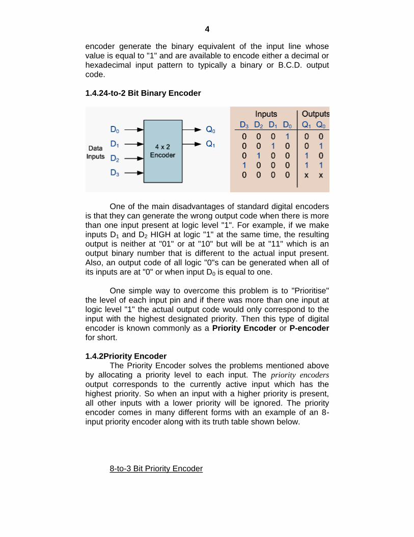
1.4.24-to-2 Bit Binary Encoder
One of the main disadvantages of standard digital encoders is that they can generate the wrong output code when there is more than one input present at logic level "1". For example, if we make inputs D1 and D2 HIGH at logic "1" at the same time, the resulting output is neither at "01" or at "10" but will be at "11" which is an output binary number that is different to the actual input present. Also, an output code of all logic "0"s can be generated when all of its inputs are at "0" or when input D0 is equal to one.
One simple way to overcome this problem is to "Prioritise"
the level of each input pin and if there was more than one input at logic level "1" the actual output code would only correspond to the input with the highest designated priority. Then this type of digital encoder is known commonly as a Priority Encoder or P-encoder for short.
1.4.2Priority Encoder
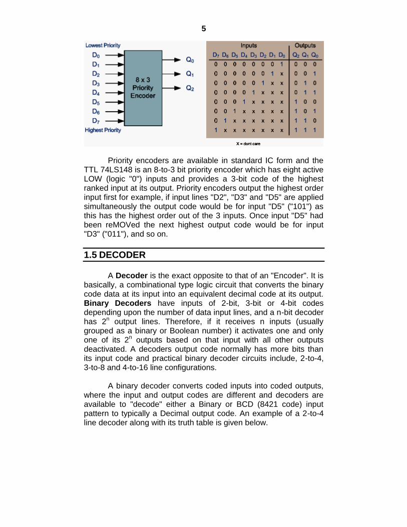
The Priority Encoder solves the problems mentioned above by allocating a priority level to each input. The priority encoders output corresponds to the currently active input which has the highest priority. So when an input with a higher priority is present, all other inputs with a lower priority will be ignored. The priority encoder comes in many different forms with an example of an 8-input priority encoder along with its truth table shown below.
8-to-3 Bit Priority Encoder
5
Priority encoders are available in standard IC form and the
TTL 74LS148 is an 8-to-3 bit priority encoder which has eight active LOW (logic "0") inputs and provides a 3-bit code of the highest ranked input at its output. Priority encoders output the highest order input first for example, if input lines "D2", "D3" and "D5" are applied simultaneously the output code would be for input "D5" ("101") as this has the highest order out of the 3 inputs. Once input "D5" had been reMOVed the next highest output code would be for input "D3" ("011"), and so on.
1.5 DECODER
A Decoder is the exact opposite to that of an "Encoder". It is
basically, a combinational type logic circuit that converts the binary code data at its input into an equivalent decimal code at its output. Binary Decoders have inputs of 2-bit, 3-bit or 4-bit codes depending upon the number of data input lines, and a n-bit decoder has 2n output lines. Therefore, if it receives n inputs (usually grouped as a binary or Boolean number) it activates one and only one of its 2n outputs based on that input with all other outputs deactivated. A decoders output code normally has more bits than its input code and practical binary decoder circuits include, 2-to-4, 3-to-8 and 4-to-16 line configurations.
A binary decoder converts coded inputs into coded outputs,
where the input and output codes are different and decoders are available to "decode" either a Binary or BCD (8421 code) input pattern to typically a Decimal output code. An example of a 2-to-4 line decoder along with its truth table is given below.
6
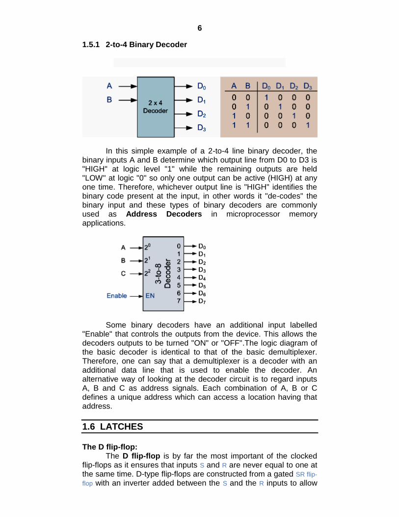
1.5.1 2-to-4 Binary Decoder
In this simple example of a 2-to-4 line binary decoder, the
binary inputs A and B determine which output line from D0 to D3 is "HIGH" at logic level "1" while the remaining outputs are held "LOW" at logic "0" so only one output can be active (HIGH) at any one time. Therefore, whichever output line is "HIGH" identifies the binary code present at the input, in other words it "de-codes" the binary input and these types of binary decoders are commonly used as Address Decoders in microprocessor memory applications.
Some binary decoders have an additional input labelled
"Enable" that controls the outputs from the device. This allows the decoders outputs to be turned "ON" or "OFF".The logic diagram of the basic decoder is identical to that of the basic demultiplexer. Therefore, one can say that a demultiplexer is a decoder with an additional data line that is used to enable the decoder. An alternative way of looking at the decoder circuit is to regard inputs A, B and C as address signals. Each combination of A, B or C defines a unique address which can access a location having that address.
1.6 LATCHES
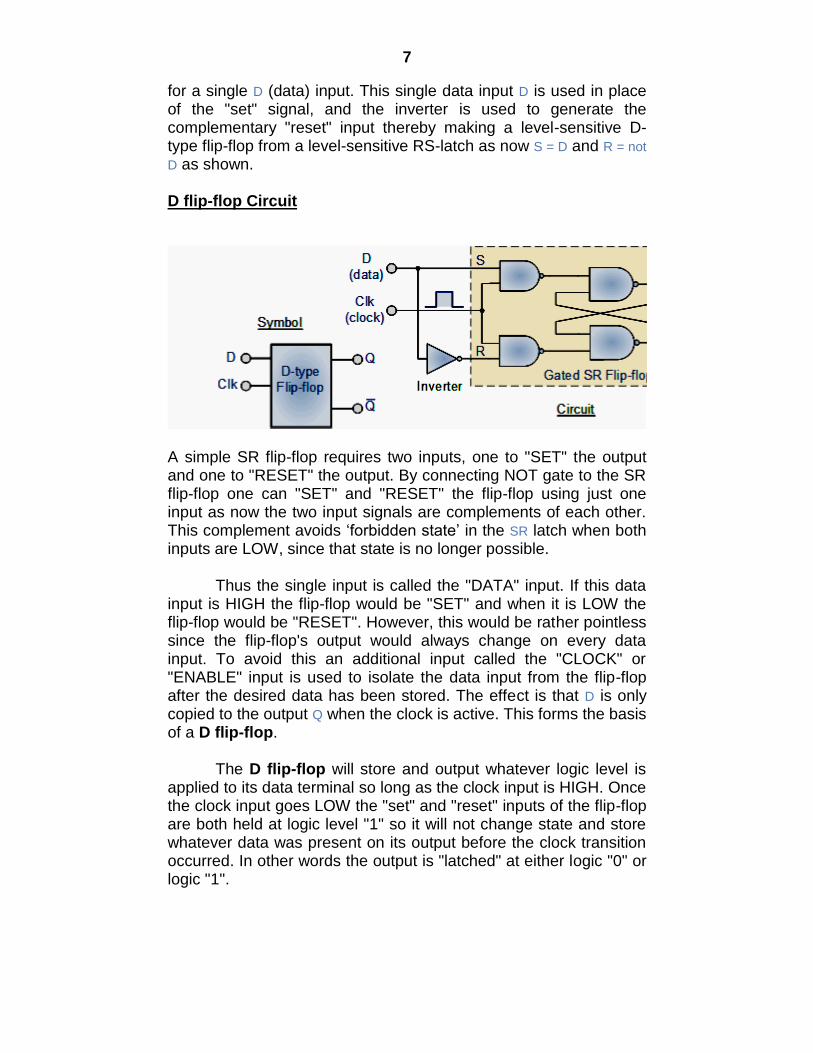
The D flip-flop: The D flip-flop is by far the most important of the clocked flip-flops as it ensures that inputs S and R are never equal to one at the same time. D-type flip-flops are constructed from a gated SR flip-
flop with an inverter added between the S and the R inputs to allow
7
for a single D (data) input. This single data input D is used in place of the "set" signal, and the inverter is used to generate the complementary "reset" input thereby making a level-sensitive D-type flip-flop from a level-sensitive RS-latch as now S = D and R = not
D as shown. D flip-flop Circuit
A simple SR flip-flop requires two inputs, one to "SET" the output and one to "RESET" the output. By connecting NOT gate to the SR flip-flop one can "SET" and "RESET" the flip-flop using just one input as now the two input signals are complements of each other. This complement avoids „forbidden state‟ in the SR latch when both inputs are LOW, since that state is no longer possible.
Thus the single input is called the "DATA" input. If this data
input is HIGH the flip-flop would be "SET" and when it is LOW the flip-flop would be "RESET". However, this would be rather pointless since the flip-flop's output would always change on every data input. To avoid this an additional input called the "CLOCK" or "ENABLE" input is used to isolate the data input from the flip-flop after the desired data has been stored. The effect is that D is only copied to the output Q when the clock is active. This forms the basis of a D flip-flop.
The D flip-flop will store and output whatever logic level is
applied to its data terminal so long as the clock input is HIGH. Once the clock input goes LOW the "set" and "reset" inputs of the flip-flop are both held at logic level "1" so it will not change state and store whatever data was present on its output before the clock transition occurred. In other words the output is "latched" at either logic "0" or logic "1".
8
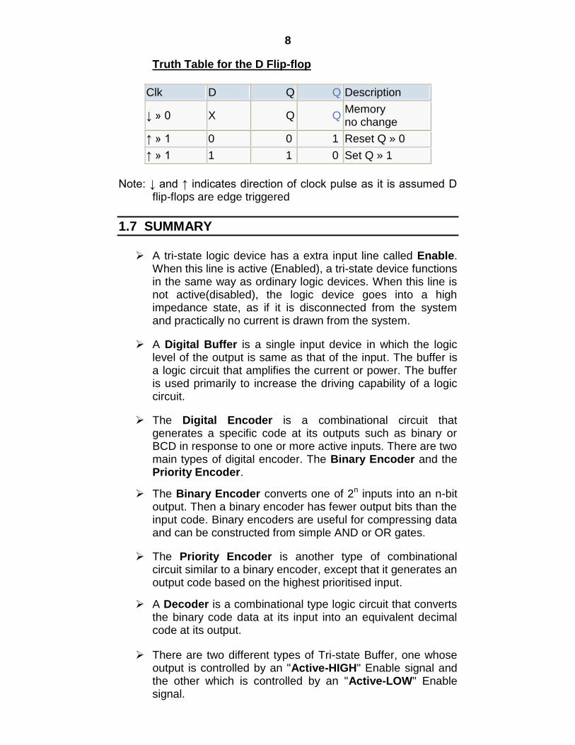
Truth Table for the D Flip-flop
Clk D Q Q Description
↓ » 0 X Q Q Memory no change
↑ » 1 0 0 1 Reset Q » 0
↑ » 1 1 1 0 Set Q » 1
Note: ↓ and ↑ indicates direction of clock pulse as it is assumed D
flip-flops are edge triggered
1.7 SUMMARY
A tri-state logic device has a extra input line called Enable.
When this line is active (Enabled), a tri-state device functions in the same way as ordinary logic devices. When this line is not active(disabled), the logic device goes into a high impedance state, as if it is disconnected from the system and practically no current is drawn from the system.
A Digital Buffer is a single input device in which the logic level of the output is same as that of the input. The buffer is a logic circuit that amplifies the current or power. The buffer is used primarily to increase the driving capability of a logic circuit.
The Digital Encoder is a combinational circuit that generates a specific code at its outputs such as binary or BCD in response to one or more active inputs. There are two main types of digital encoder. The Binary Encoder and the Priority Encoder.
The Binary Encoder converts one of 2n inputs into an n-bit output. Then a binary encoder has fewer output bits than the input code. Binary encoders are useful for compressing data and can be constructed from simple AND or OR gates.
The Priority Encoder is another type of combinational circuit similar to a binary encoder, except that it generates an output code based on the highest prioritised input.
A Decoder is a combinational type logic circuit that converts the binary code data at its input into an equivalent decimal code at its output.
There are two different types of Tri-state Buffer, one whose output is controlled by an "Active-HIGH" Enable signal and the other which is controlled by an "Active-LOW" Enable signal.
9
1.8 REVIEW QUESTIONS
1. What do you mean by tri-state devices? 2. With the help of a neat symbol explain tri-state buffer. 3. State function of buffer. 4. Explain different types of encoder. 5. With the help of neat block diagram explain 4 to 2 encoder. 6. What do you mean by priority encoder? 7. With the help of neat block diagram explain 8 to 3 encoder. 8. Explain decoder in detail. 9. With the help of neat block diagram explain 3 to 8 decoder. 10. Explain the working of D flipflop.
1.9 REFERENCE
Microprocessor Architecture, Programming, and Applications With the 8085 by Ramesh Gaonkar, Publisher: Prentice Hall
Digital Principles and application by Malvino and Leach,
Publisher: McGraw-Hill
10
2
MEMORY
Unit Structure
1.1 Introduction
1.2 Memory
1.3 Random Access Memory (RAM)
1.4 Read Only Memory (ROM)
1.5 Nonvolatile RAM (NVRAM)
1.6 Memory Interfacing
1.7 Summary
1.8 Review Questions
1.9 Reference
2.0 OBJECTIVES
After studying this chapter you should be able to Understand the different types of memory used in 8085 Distinguish between SRAM & DRAM Understand different types ROM Understand the different technique of memory interfacing
1.6 INTRODUCTION
Many types of memory devices are available for use in
modern computer systems. You must be aware of the differences between them andunderstand how to use each type effectively. As you are reading, try to keep in mind that thedevelopment of these devices took several decades and that there are significant physicaldifferences in the underlying hardware. The names of the memory types frequently reflect the historical nature of the development process and are often more confusing than insightful.
1.2 MEMORY
Memory is the storage device which can be used to store
monitor program, users program or users data.So memory is an important component of the microprocessor based system, which
11
will allow you to store program and data.The memory consists of the thousands of memory cells arranged to store data.Each memory cell is capable of storing 1 bit of the data.Hence, to use memory to store programs or data of user or system, memory must be interfaced with microprocessor properly, so that it can be accessed while reading or writing data or program from/to it .In the same way, input and output devices are also required to read or write data out from the microprocessor using input device such as keyboard or output device using console. So, these devices must be interface properly with the microprocessor so that user can read data from input device and write data to the output device
1.3 RANDOM ACCESS MEMORY (RAM)
Random accessmeans that the stored data can be accessed
in any order, which is in contrast to the morerestricted access provided by other memory systems, such as tape and disk drive. Theaccess time to any piece of data stored on in RAM is essentially the same.
RAM is normally used in computer systems for main memory
or primary storage. This iswhere running programs and the data they use are stored. Moving data from primarystorage to the processor requires only a few cycles, although retrieving data from a harddrive can take considerable longer. For this reason, modern operating systems runprimarily in RAM, and as they load and run additional applications, they move theseprograms and their data into RAM for faster processing.
RAM can be categorized as volatile or non-volatile. Volatile
means that all data is lostwhen the chip is powered down. Most computers incorporate two types of volatile RAM: static and dynamic. Althoughboth types require constant electrical current to function, they have some importantdifferences.
1.3.1 Dynamic RAM (DRAM)
Dynamic RAM is less expensive, and therefore it is the most widely used.
When a computer is said to have 512 megabytes or one gigabyte of RAM, the specification refers to dynamic RAM (DRAM). DRAM stores each bit of information in a separate capacitor on the integrated circuit. The DRAM chip requires only one transistor and one capacitor for each bit of storage. This makes it both cheap and space efficient. One disadvantage with using capacitors for storage is that they gradually dissipate their charge, so the charge must be refreshed regularly (current specifications are for there fresh to
12
occur every 64 milliseconds or less). This refresh requirement is what makesthis technology dynamic. 1.3.2 DRAM controller
The DRAM controller is an extra piece of hardwareplaced between the processor and the memory chips. Its main purpose is to performthe refresh operations required to keep your data alive in the DRAM.
Almost all DRAM controllers require a short initialization
sequence that consists ofone or more setup commands. The setup commands tell the controller about the hardware interface to the DRAM and how frequently the data there must berefreshed. If the DRAM in your system does not appear to be workingproperly, it could be that the DRAM controller either is not initialized or has beeninitialized incorrectly. 1.3.3 Static RAM (SRAM)
Static RAM (SRAM) has the advantage of being faster than DRAM, although the disadvantage is that it is more expensive. SRAM is static in the sense that it doesn‟t require constant electrical refreshes; however, it still requires constant current to maintainthe voltage differentials. SRAM generally requires less power than DRAM.
Each bit in a SRAM chip requires a cell of six transistors, although DRAM needs only one transistor and one capacitor. This means that SRAM cannot achieve the storage densities of the DRAM family. As with DRAM, SRAM chips are mostly large arrays of these cells of transistors.The two primary applications of SRAM are embedded use and in computers.
1.4 READ ONLY MEMORY (ROM)
Memories in the ROM family are distinguished by the
methods used to write new data tothem and the number of times they can be rewritten. Thisclassification reflects the evolution of ROM devices from hardwired to one-timeprogrammable to erasable-and-programmable. A common feature across all these devices istheir ability to retain data and programs forever, even during a power failure.
There are several types ofread only memory (ROM), although most are obsolete. These ROMs are called read onlybecause they cannot be modified by the casual user (and some types cannot be modifiedat all). ROMs have traditionally been used
13
in computer systems to store configurationdata, such as bootstrap or BIOS code, which requires fast access. 1.4.1 Masked ROMs
The very first ROMs were hardwired devices that contained a preprogrammed set of data orinstructions. The contents of the ROM had to be specified before chip production, so theactual data could be used to arrange the transistors inside the chip. Hardwired memories arestill used, though they are now called "masked ROMs" to distinguish them from other typesof ROM. The main advantage of a masked ROM is a low production cost. Unfortunately, thecost is low only when hundreds of thousands of copies of the same ROM are required.it was often usedto contain the startup code (bootstrap) for early microcomputers.
1.4.2 Programmable Read Only Memory (PROM)
One step up from the masked ROM is the PROM (programmable ROM), which is purchasedin an unprogrammed state.The process of writing your data to thePROM involves a special piece of equipment called a device programmer. The deviceprogrammer writes data to the device one word at a time, by applying an electrical charge tothe input pins of the chip. Once a PROM has been programmed in this way, its contents cannever be changed. If the code or data stored in the PROM must be changed, the current devicemust be discarded. As a result, PROMs are also known as one-time programmable (OTP)devices.
ThePROM is a cheaper and more flexible approach than
mask ROM, although each PROMcan still be programmed only once. PROMs are reliable, permanent, and relatively fast.They are still in limited use. 1.4.3 Erasable Programmable Read Only Memory (EPROM)
An EPROM (erasable-and-programmable ROM) is programmed in exactly the same manneras a PROM. However, EPROMs can be erased and reprogrammed repeatedly. To erase anEPROM, you simply expose the device to a strong source of ultraviolet light. (There is a"window" in the top of the device to let the ultraviolet light reach the silicon.) By doing this,you essentially reset the entire chip to its initial-unprogrammed-state. EPROM chips preserve their data for roughly10 to 20 years and allow for an unlimitednumber of reads. The erasing window is kept covered by a foil label to prevent erasure byexposure to sunlight.
The most popular use of EPROMs in computer systems was
to storethe BIOS in older PC systems.Though more expensivethan
14
PROMs, their ability to be reprogrammed makes EPROMs an essential part of thesoftware development and testing process. 1.4.4 Electronically Erasable Programmable Read Only Memory (EEPROM)
The electronically erasable programmable read only memory (EEPROM) has largelysupplanted all other types of ROM in the current generation of computing devices. Thecapacity of EEPROMs ranges up to hundreds of kilobits. This is now the preferredtechnology for storing the BIOS in personal computers.
As the term electronically erasable implies, EEPROMs can
be erased and rewritten,usually by creating a high-voltage pulse on the chip. This rewriting eventually damagesthe layer of insulating material on the chip, so the number of writes is limited. Althoughearly models would fail after 100 write-erase cycles, current EEPROMs can sustain onemillion write-erases or more. Any byte within an EEPROM can be erased and rewritten. Once written, thenew data will remain in the device forever-or at least until it is electrically erased. Thetradeoff for this improved functionality is mainly higher cost. 1.4.5 Flash Memory
Flash memory is the most recent advancement in memory technology. It combines all the bestfeatures of the memory devices described thus far. Flash memory devices are high density,low cost, nonvolatile, fast (to read, but not to write), and electrically reprogrammable.Although flash memory is erased only one blockor page at a time, it is much less expensive than EEPROM.
Theseadvantages are overwhelming and the use of Flash memory has increased dramatically inembedded systems as a direct result. From a software viewpoint, Flash and EEPROMtechnologies are very similar. The major difference is that Flash devices can be erased onlyone sector at a time, not byte by byte. Typical sector sizes are in the range of 256 bytes to 16kilobytes. Despite this disadvantage, Flash is much more popular than EEPROM and israpidly displacing many of the ROM devices as well.
1.5 NONVOLATILE RAM (NVRAM)
An NVRAM is usually just anSRAM with a battery backup.
When the power is turned on, the NVRAM operates just likeany other SRAM. But when the power is turned off, the NVRAM draws just enough electricalpower from the battery to retain its current contents. NVRAM is fairly common in embeddedsystems. However,
15
it is very expensive-even more expensive than SRAM-so its applicationsare typically limited to the storage of only a few hundred bytes of system-critical informationthat cannot be stored in any better way.
1.6 MEMORY INTERFACING
In computer systems, 1K=1024; therefore 1Kbyte memory
chip has 1024 registers with 8 bits each. Similarly, a group of 256 registers is defined as one page and each register is viewed as a line to write on. This is analogous to a notebooks containing various pages, with each page having a certain numbers of lines. With this analogy, 1Kbyte memory as a chip of four pages (1024/256=4) with each page having 256 registers. With two hex digits, 256 registers can be numbered from 00H to FFH; 1024 registers can be numbered from four digits from 0000H to 03FFH. The high order two digits of 1 K memory are representing 4 pages (00, 01, 02 & 03)
1.6.1 Memory Address
In computer science, a memory address is a unique identifier for a memory location at which a CPU or other device can store a piece of data for later retrieval.In modern byte- addressable computers, each address identifies a single byte of storage.Some microprocessors were designed to be word-addressable, so that the typical storage unit was actually larger than a byte.
Each memory chip like RAM, ROM, EPROM, E2PROM and
DRAM have numbers of pins and these pins are used to accept different kinds of signals.Normally every memory chip has pins for address, data, control signals and chip select signals.
1.6.2 Address Pins
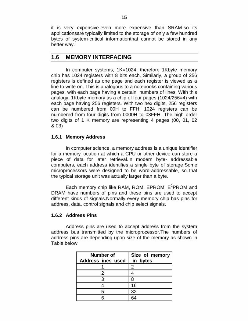
Address pins are used to accept address from the system address bus transmitted by the microprocessor.The numbers of address pins are depending upon size of the memory as shown in Table below
Number of Address ines used
Size of memory in bytes
1 2
2 4
3 8
4 16
5 32
6 64
16
7 128
8 256
9 512
10 1024 ≈ 1k
11 2048 ≈ 2k
12 4096 ≈ 4k
13 8192 ≈ 8k
14 16384 ≈ 16k
15 32768 ≈ 32k
16 65536 ≈ 64k
In case of 8085 microprocessor the address bus is 16 bit wide; it can address 65,536 locations i.e. 64 Kbytes of memory.
1.6.3 CS (Chip Select) or CE (Chip Enable) Pin
This signal of the memory chip is ACTIVE LOW and acts as master enable pin for read or write operation.Hence, for every read or write operation, this signal must be low otherwise no operation will be performed. 1.6.4 WR (Write Control Signal) Pin
This is an active low input control signal used to write data to the memory location whose address is available on address lines if chip select signal is enable. This signal is available on system control bus and generated by the microprocessor or other master in the system such as DMA controller or co-processor.
1.6.5 RD (Read Control Signal) Pin
This is an active low input control signal used to read data from the memory location whose address is available on address lines if chip select signal is enable. This signal is available on system control bus and generated by the microprocessor or other master in the system such as DMA controller or co-processor. 1.6.6 Chip Select Logic
Chip select logic can be developed using either combination of different gates such as AND, NAND, NOT etc. or decoders. 1.6.6.1 Using Logic Gates
Now take an example of interfacing of 2K of RAM with the microprocessor 8085, the 8085 is an 8 bit microprocessor. Hence all 8 lines of data bus can be directly connected after de-
17
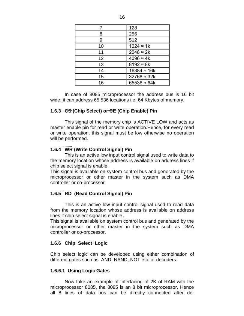
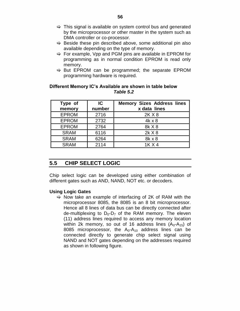
multiplexing to D0-D7 of the RAM memory. The eleven (11) address lines required to access any memory location within 2K memory, so out of 16 address lines (A0-A15) of 8085 microprocessor, the A0-A10 address lines can be connected directly memory chip. Remaining address lines A11-A15to generate chip select signal using NAND and NOT gates depending on the addresses required as shown in following figure.
Fig 2.1 Chip select using NAND gates For generation of chip select we are using NAND gate, when input to NAND gate are all logic 1, then output of NAND gate will be logic 0 and for all other combination the output will be logic 1. The chip select is active low signal, hence all inputs of the NAND gates must be logic 1 to generate chip select signal as given below.
A15 A14 A13 A12 A11
1 0 0 0 0
Hence addresses map of the 2K of RAM is given below.
A
15 A
14 A
13 A
12 A
11 A
10 A
9 A
8 A
7 A
6 A
5 A
4 A
3 A
2 A
1 A
0 ADDRESS
1 0 0 0 0 0 0 0 0 0 0 0 0 0 0 0 8000H
1 0 0 0 0 1 1 1 1 1 1 1 1 1 1 1 87FFH
Used for chip select Decoder logic
Connected to A – A10 2 K RAM
18
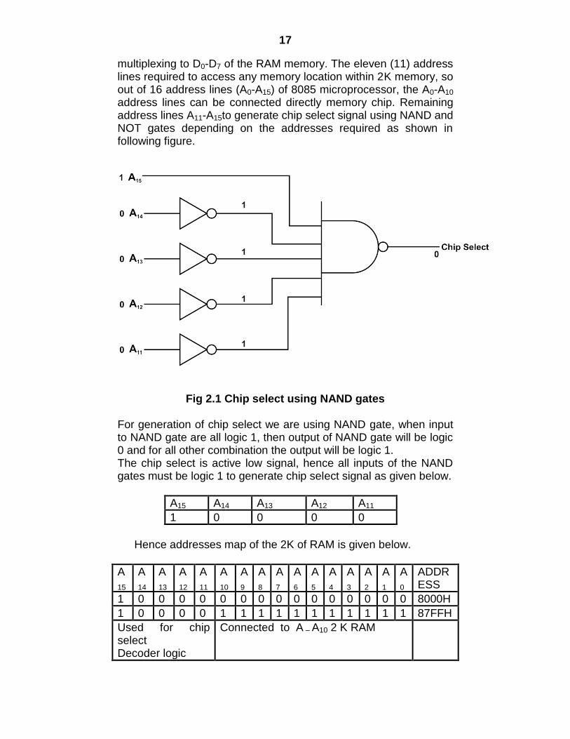
The interfacing diagram of 2K X 8 RAM is shown in following figure
Fig. 2.2 Interfacing of 2K X 8 RAM
1.6.6.2 Using Decoder
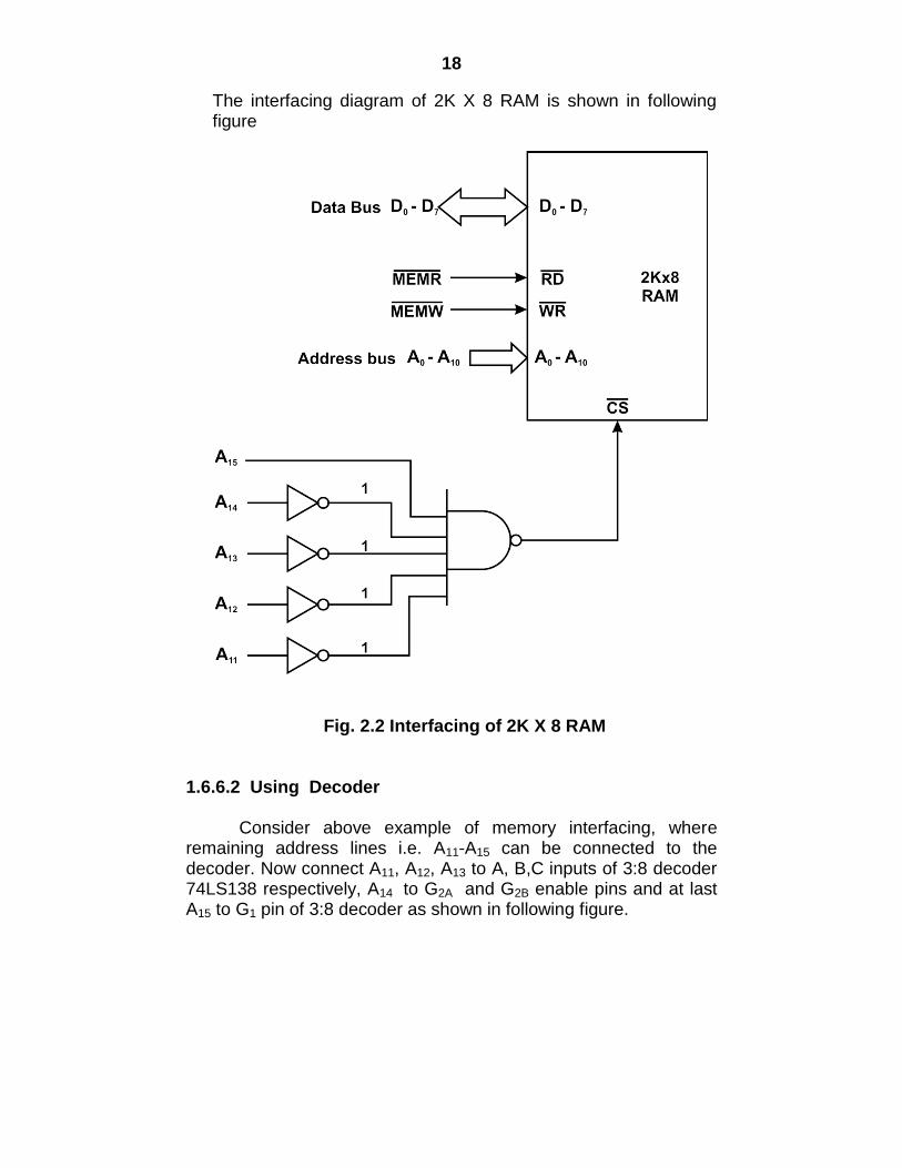
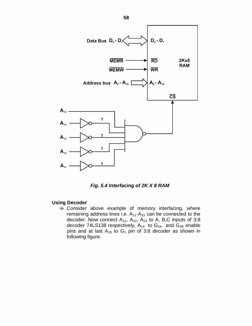
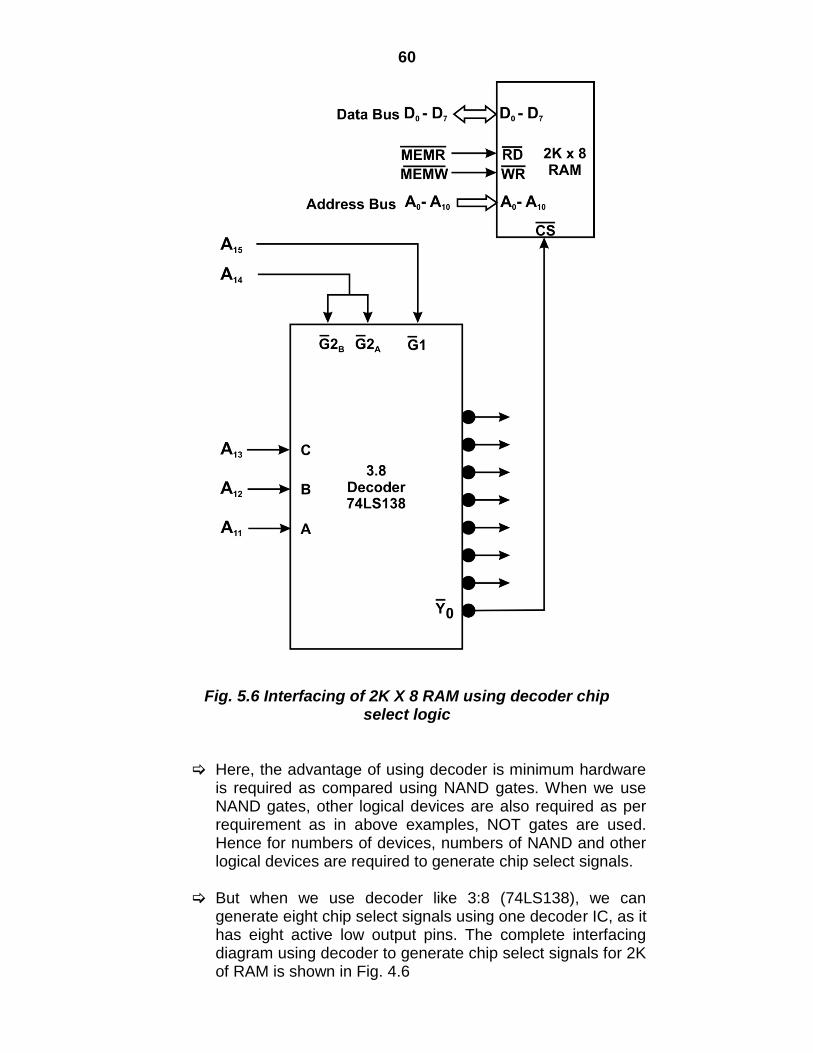
Consider above example of memory interfacing, where remaining address lines i.e. A11-A15 can be connected to the decoder. Now connect A11, A12, A13 to A, B,C inputs of 3:8 decoder 74LS138 respectively, A14 to G2A and G2B enable pins and at last A15 to G1 pin of 3:8 decoder as shown in following figure.
19
Fig. 2.3Using decoder
After making the connection as shown above, the address map of 2K RAM will be same as specified above.
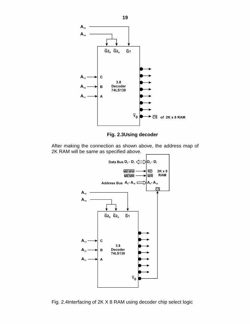
Fig. 2.4Interfacing of 2K X 8 RAM using decoder chip select logic
20
Here, the advantage of using decoder is minimum hardware is required as compared using NAND gates. When we use NAND gates, other logical devices are also required as per requirement as in above examples, NOT gates are used. Hence for numbers of devices, numbers of NAND and other logical devices are required to generate chip select signals.
But when we use decoder like 3:8 (74LS138), we can generate eight chip select signals using one decoder IC, as it has eight active low output pins. The complete interfacing diagram using decoder to generate chip select signals for 2K of RAM is shown in Fig. 2.4
1.7 SUMMARY
Most computers incorporate two types of volatile RAM: static and dynamic.
DRAM stores each bit of information in a separate capacitor
on the integrated circuit. With using capacitors for storage is that they gradually dissipate their charge, so the charge must be refreshed regularly.
The DRAM controller is an extra piece of hardware placed
between the processor and the memory chips. Its main purpose is to perform the refresh operations required to keep your data alive in the DRAM.
Static RAM (SRAM) has the advantage of being faster than
DRAM, although the disadvantage is that it is more expensive.
The process of writing your data to thePROM involves a
special piece of equipment called a device programmer. EPROMs can be erased and reprogrammed repeatedly. To
erase anEPROM, you simply expose the device to a strong source of ultraviolet light.
EEPROMs can be erased and rewritten,usually by creating a
high-voltage pulse on the chip. Flash memory devices are high density,low cost, nonvolatile,
fast (to read, but not to write), and electrically reprogrammable.
An NVRAM is usually just anSRAM with a battery backup.
21
In case of 8085 microprocessor the address bus is 16 bit wide; it can address 65,536 locations i.e. 64 Kbytes of memory.
Chip select logic can be developed using either combination
of different gates such as AND, NAND, NOT etc. or decoders.
1.8 REVIEW QUESTIONS
Q.1 Distinguish between SRAM & DRAM. Q.2 Write a short note on RAM. Q.3 Explain different types of ROM. Q.4 Distinguish between EPROM & EEPROM. Q.5 Write a short note on Flash memory. Q.6 Explain memory interfacing in 8085. Q.7 Explain control signalsWR , RD and chip select logic.
1.9 REFERENCE
Microprocessor Architecture, Programming, and Applications
With the 8085 by Ramesh Gaonkar, Publisher:Prentice Hall Programming Embedded Systems in C and C++ by Michael
Barr, Publisher: O'Reilly
22
3
INTRODUCTION TO 8085 MICROPROCESSOR
Topics Covered:
3.1 Introduction
3.2 Organization of Microprocessor based System
3.3 Features of 8085 Microprocessor
3. 1 INTRODUCTION
The microprocessor [MPU] is a programmable digital device, designed with registers, flip-flops and timing elements.
The microprocessor has a set of instructions, designed internally, to manipulate data and communicate with peripherals. This process of data manipulation and communication is determined by the logic design of the microprocessor, called architecture.
The microprocessor can be programmed to perform functions on given data by selecting necessary instructions from its set.
These instructions are given to the microprocessor by writing them into its memory.
Writing instructions and data is done through input device such as keyboard.
The functions performed by microprocessor can be classified into following categories:
Microprocessor – initiated operations.
Internal operations.
Peripheral (or eternally initiated) operations.
Microprocessor – Initiated operations and 8085 Bus organization:
The MPU performs primarily four operations:
1. Memory Read: Reads data (or instructions) from memory.
2. Memory Write: Writes data (or instructions) into memory.
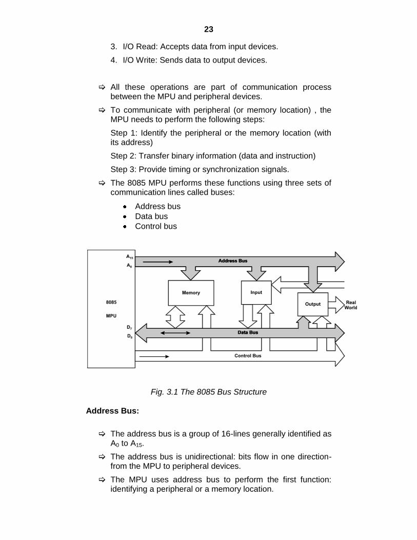
23
3. I/O Read: Accepts data from input devices.
4. I/O Write: Sends data to output devices.
All these operations are part of communication process between the MPU and peripheral devices.
To communicate with peripheral (or memory location) , the MPU needs to perform the following steps:
Step 1: Identify the peripheral or the memory location (with its address)
Step 2: Transfer binary information (data and instruction)
Step 3: Provide timing or synchronization signals.
The 8085 MPU performs these functions using three sets of communication lines called buses:
Address bus
Data bus
Control bus
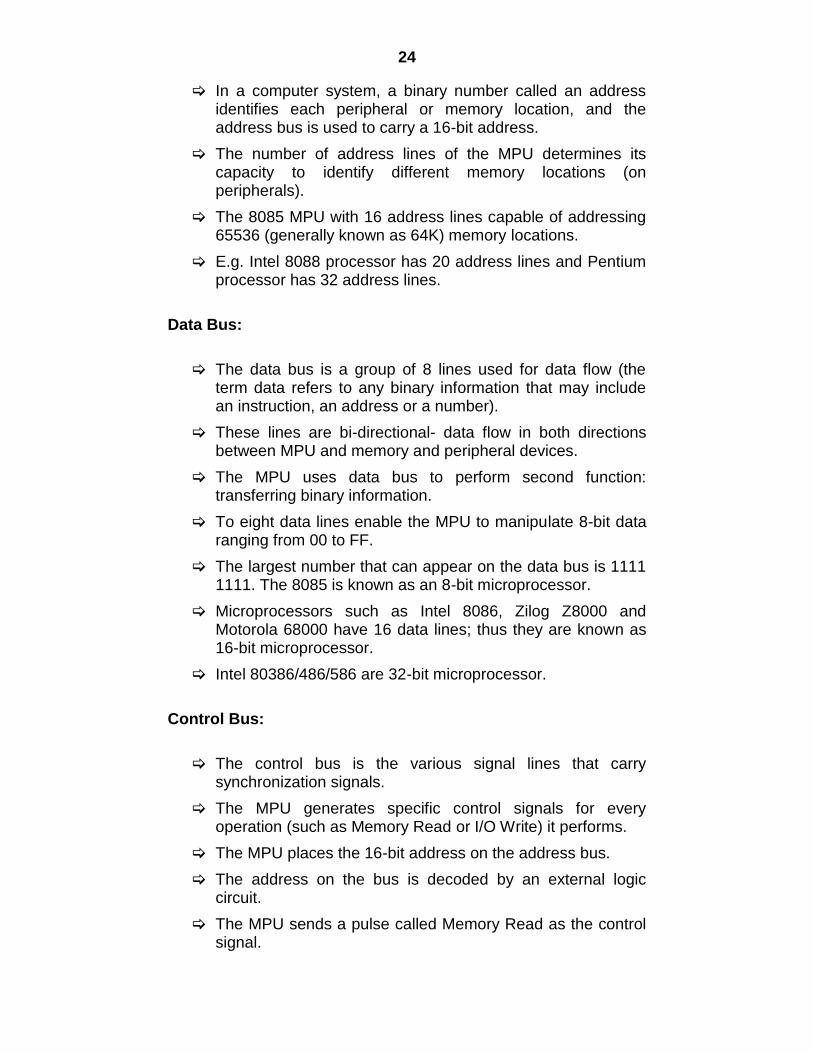
Fig. 3.1 The 8085 Bus Structure Address Bus:
The address bus is a group of 16-lines generally identified as A0 to A15.
The address bus is unidirectional: bits flow in one direction-from the MPU to peripheral devices.
The MPU uses address bus to perform the first function: identifying a peripheral or a memory location.
24
In a computer system, a binary number called an address identifies each peripheral or memory location, and the address bus is used to carry a 16-bit address.
The number of address lines of the MPU determines its capacity to identify different memory locations (on peripherals).
The 8085 MPU with 16 address lines capable of addressing 65536 (generally known as 64K) memory locations.
E.g. Intel 8088 processor has 20 address lines and Pentium processor has 32 address lines.
Data Bus:
The data bus is a group of 8 lines used for data flow (the term data refers to any binary information that may include an instruction, an address or a number).
These lines are bi-directional- data flow in both directions between MPU and memory and peripheral devices.
The MPU uses data bus to perform second function: transferring binary information.
To eight data lines enable the MPU to manipulate 8-bit data ranging from 00 to FF.
The largest number that can appear on the data bus is 1111 1111. The 8085 is known as an 8-bit microprocessor.
Microprocessors such as Intel 8086, Zilog Z8000 and Motorola 68000 have 16 data lines; thus they are known as 16-bit microprocessor.
Intel 80386/486/586 are 32-bit microprocessor.
Control Bus:
The control bus is the various signal lines that carry synchronization signals.
The MPU generates specific control signals for every operation (such as Memory Read or I/O Write) it performs.
The MPU places the 16-bit address on the address bus.
The address on the bus is decoded by an external logic circuit.
The MPU sends a pulse called Memory Read as the control signal.
25
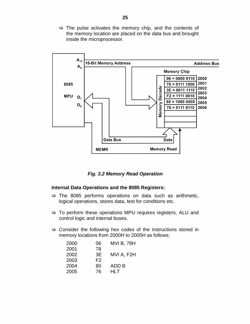
The pulse activates the memory chip, and the contents of the memory location are placed on the data bus and brought inside the microprocessor.
Fig. 3.2 Memory Read Operation
Internal Data Operations and the 8085 Registers:
The 8085 performs operations on data such as arithmetic, logical operations, stores data, test for conditions etc.
To perform these operations MPU requires registers, ALU and
control logic and internal buses. Consider the following hex codes of the instructions stored in
memory locations from 2000H to 2005H as follows:
2000 06 MVI B, 78H 2001 78 2002 3E MVI A, F2H 2003 F2 2004 80 ADD B 2005 76 HLT
26
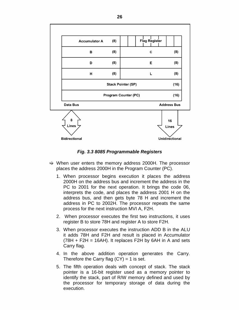
Fig. 3.3 8085 Programmable Registers
When user enters the memory address 2000H. The processor places the address 2000H in the Program Counter (PC).
1. When processor begins execution it places the address 2000H on the address bus and increment the address in the PC to 2001 for the next operation. It brings the code 06, interprets the code, and places the address 2001 H on the address bus, and then gets byte 78 H and increment the address in PC to 2002H. The processor repeats the same process for the next instruction MVI A, F2H.
2. When processor executes the first two instructions, it uses register B to store 78H and register A to store F2H.
3. When processor executes the instruction ADD B in the ALU it adds 78H and F2H and result is placed in Accumulator (78H + F2H = 16AH). It replaces F2H by 6AH in A and sets Carry flag.
4. In the above addition operation generates the Carry. Therefore the Carry flag (CY) = 1 is set.
5. The fifth operation deals with concept of stack. The stack pointer is a 16-bit register used as a memory pointer to identify the stack, part of R/W memory defined and used by the processor for temporary storage of data during the execution.
27
Peripheral or Externally Initiated Operations: External devices (or signals) can initiate the following
operations, for which individual pins on the microprocessor chip are assigned: Reset, Interrupt, Ready, Hold.
Reset: When an external key activates RESET key, all internal operations are suspended and the program counter is cleared (it holds 0000H). Now program execution begins at the zero memory address. Interrupt: The microprocessor can be interrupted from the normal execution of instructions and asked to execute some other instructions called a service routine. The microprocessor resumes its operation after completing the service routine. Ready: The 8085 has a pin called READY. If the signal at this READY pin is low, the microprocessor enters into a Wait state. This signal is used primarily to synchronize slower peripherals with the microprocessor. Hold: When the HOLD pin is activated by an external signal, the microprocessor relinquishes control of buses and allows the external peripherals to use them. HOLD signal is used in Direct Memory Access (DMA) data transfer.
3.2 ORGANIZATION OF MICROPROCESSOR BASED SYSTEM
A microprocessor based system has standard components like memory, timing and input/output.
Depending on the application, other components are added
such as digital to analog converter, interval timer, math coprocessors, interrupt controller etc.
Figure below shows the basic block diagram of
microprocessor based system containing some standard components.
28
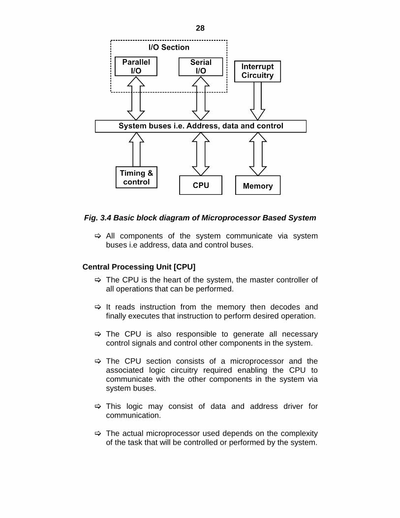
Fig. 3.4 Basic block diagram of Microprocessor Based System
All components of the system communicate via system buses i.e address, data and control buses.
Central Processing Unit [CPU]
The CPU is the heart of the system, the master controller of all operations that can be performed.
It reads instruction from the memory then decodes and
finally executes that instruction to perform desired operation. The CPU is also responsible to generate all necessary
control signals and control other components in the system. The CPU section consists of a microprocessor and the
associated logic circuitry required enabling the CPU to communicate with the other components in the system via system buses.
This logic may consist of data and address driver for
communication. The actual microprocessor used depends on the complexity
of the task that will be controlled or performed by the system.
29
Memory It has two components i.e read only memory [ROM] and
random access memory [RAM]. Sometimes other semiconductor memories such as EPROM,
PROM, E2PROM can be used and usually contains monitor programs or BIOS program.
The ROM included provides the system with its intelligence,
which is needed at the start up (power on) to configure or initialize peripheral.
The RAM is of again two types i.e static and dynamic RAM.
The static RAM is fast and easy to interface, but comes in
small sizes and costly. The dynamic RAM is slow and requires numerous refreshing
cycles to retain the stored data, even so dynamic RAM is the choice for large memory where large amount of data can be stored as these RAM‟s are cheaper in cost.
Both static and dynamic RAM lose their information, when
power is turned off, which may cause a problem in certain situations.
In the latest systems, non-volatile memory (NVM) is used
which retains its information even when power is turned off. NVM comes in a small size; hence it is used to store only the
most important information during power failure. Timing and Control This section of the system governs all system timing and
thus is responsible for the proper operation of the entire system hardware.
The timing section usually consists of a crystal oscillator and
timing circuitry set to operate the microprocessor at its specified clock rate.
I/O Section Some system may require the I/O peripherals for the some
specific purpose such as keyboard for entering data and program, monitor to display results, printers to get hard copy etc.
30
So, microprocessor can communicate with these peripheral either using parallel or serial communication port.
Serial communication is slow but it has advantage of simplicity i.e requires only two wires for receive, transmit and ground.
Serial communication is easily adapted for use in fibre optics cables.
On other hand, parallel I/O is faster but requires more lines depending on size of data bus hence it is costly for implementation.
A parallel I/O operation can be used to transfer data to/from a hard disk, reading switch information, controlling indicator lights, transferring data to A/D or D/A converter and other types of parallel devices.
Interrupt Circuitry When a microprocessor used in control applications, there
will be times when the system must respond to special external circumstances.
Such circumstances interrupt the microprocessor from its
normal execution to service the unexpected event. The system software is designed to handle such unexpected
event. Interrupts are used to perform a special task such as real
time clocks, multitasking capability and fast I/O operations. The interrupt circuitry needed from system to system will
vary depending on the applications.
3.3 FEATURES OF 8085 MICROPROCESSOR
8085 microprocessor is an 8-bit microprocessor. It can accept process or provide 8-bit data simultaneously. It operates on a single +5v power supply connected at Vcc and
power supply ground is connected to Vss. It can operate on clock cycle with 50% duty cycle. It has on chip clock generator. This internal clock generator requires tuned circuit like LC, RC
or crystal. It can operate with a 3 MHz clock frequency. It has 16 address lines; hence it can access 64 kbytes of
memory. It provides 8 bit I/O addresses to access 256 I/O ports.
31
3.4 EXERCISE
1. What is a Microprocessor? 2. Explain the classification of the functions performed by the
Microprocessor. 3. List the four operations commonly performed by the
Microprocessor. 4. Explain the three set of communication lines used to perform
the functions of 8085 microprocessors. 5. What is a bus? 6. Specify the function of the address bus and the direction of
the information flow on the address bus. 7. Why is the data bus bidirectional? 8. Explain Control Bus. 9. What are the various operations performed by the 8085
Microprocessor on the data? 10. Specify the four control signals commonly used by the 8085
microprocessor. 11. Explain with diagram Microprocessor Based System. 12. What are the features of 8085 Microprocessor?
3.5 REFERENCES
Computer System Architecture – M. Morris Meno, PHI, 1998
Computer Architecture and Organization - John P Hayes, McGraw Hill, 1998
Digital Computer Fundamentals – Malvino
Digital Computer Fundamentals – Thomas C Bartee, TMG
Computer Organization and Architecture – William Stallings
Microprocessor Architecture and Programming and Applications with the 8085 – R.S. Gaonkar, PRI
4
32
4 PIN DIAGRAM AND ARCHITECTURE OF
8085 MICROPROCESSOR
Topics Covered:
4.1 Pin Diagram of 8085 Microprocessor with description
4.2Architecture of 8085 Microprocessor
4.1 PIN DIAGRAM OF 8085 MICROPROCESSOR WITH DESCRIPTION
The 8085 microprocessor 8085 is a 8-bit general purpose microprocessor capable of
addressing 64K memory. The device has 40 pins and requires +5V single power supply. It can operate with 3MHz single-phase clock.
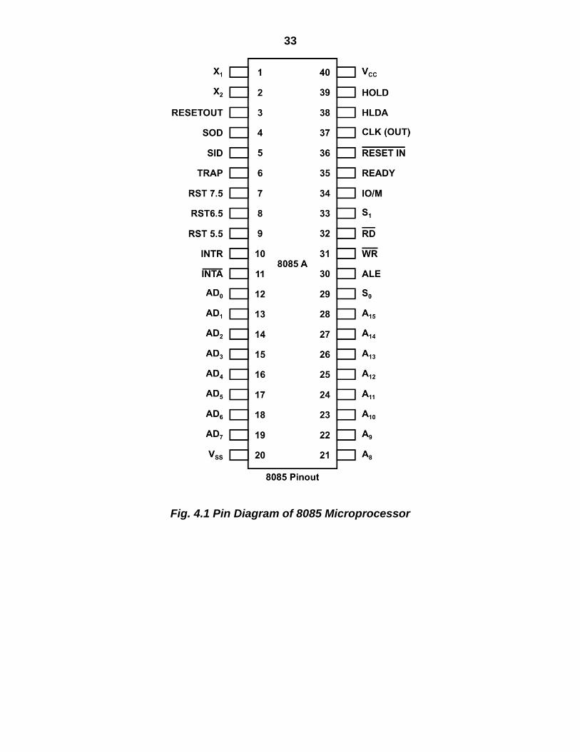
The logic pin out of the 8085-microprocessor signals can be
classified into six groups: 1. Address bus 2. Multiplexed Address/Data bus 3. Control and status signals 4. Power supply and clock frequency 5. Externally initiated signals, including interrupts 6. Serial I/O ports
33
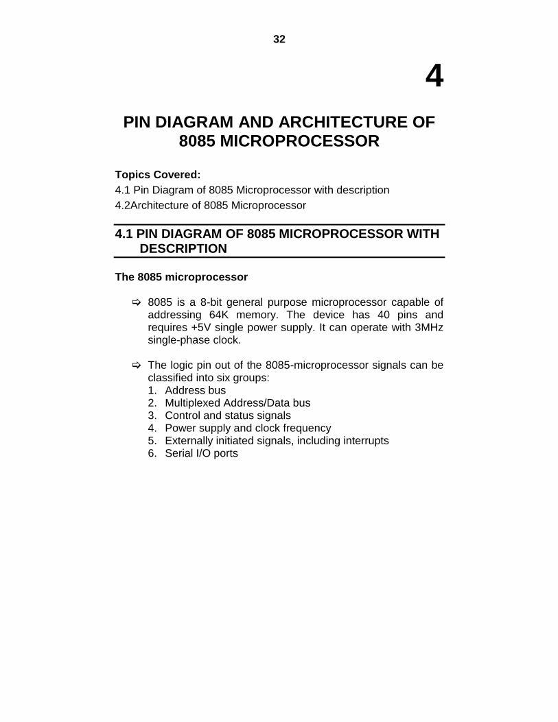
Fig. 4.1 Pin Diagram of 8085 Microprocessor
34
Fig. 4.2 The Signals of 8085 Microprocessor Address Bus: The 16 address lines are split into two parts A15-A8 and AD7-
AD0. Higher order bus is unidirectional and the signal lines AD7-AD0 are used for a dual purpose.
Multiplexed Address/Data Bus: The signal lines AD7-AD0 are bi-directional. They are used
as lower order address bus as well as data bus. In executing an instruction, during the earlier part of the cycle, these lines are used as low order address bus. During later part of cycle these lines are used are data bus.
35
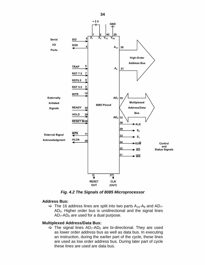
Control and Status Signals: This group of signals includes two control signals RD and
WR, three status signals (IO/M, S1 and S0) to identify nature of operation.
ALE (Address Latch Enable) : This is a +ve pulse generated every time when 8085 begins an operation(machine cycle); it indicates that the bits on AD7-AD0 are address bits. This signal is primarily used to latch the low-order address bus.
RD-(Read) : This is a Read control signal(Active low). This signal indicates that the selected I/O or memory device is to be read and data are available on data bus.
WR-(Write) : This is a Write control signal(Active low). This signal indicates that the data on the data bus are to be written into a selected memory or I/O location.
IO/M : This is a status signal used to differentiate between I/O and memory operations. When it is high, it indicates an I/O operation; when it is low, it indicates a memory operation. This signal is combined with RD and WR to generate I/O and memory control signals.
S1 and S0 : These status signals are similar to IO/M and used to identify various operation as follows
Table 4.1 8085 Machine Cycle Status and Control
Signals
Machine Cycle Status Control signals IO/M S1 S0
Opcode Fetch 0 1 1
RD=0
Memory Read 0 1 0 RD=0
Memory Write 0 0 1 WR=0
I/O Read 1 1 0 RD=0
I/O Write 1 0 1 WR=0
Interrupt Acknowledge
1 1 1 INTA=0
Halt Z 0 0 RD,WR=Z
and INTA=1
Hold Z X X
Reset Z X X
Z= High impedance X=Unspecified
36
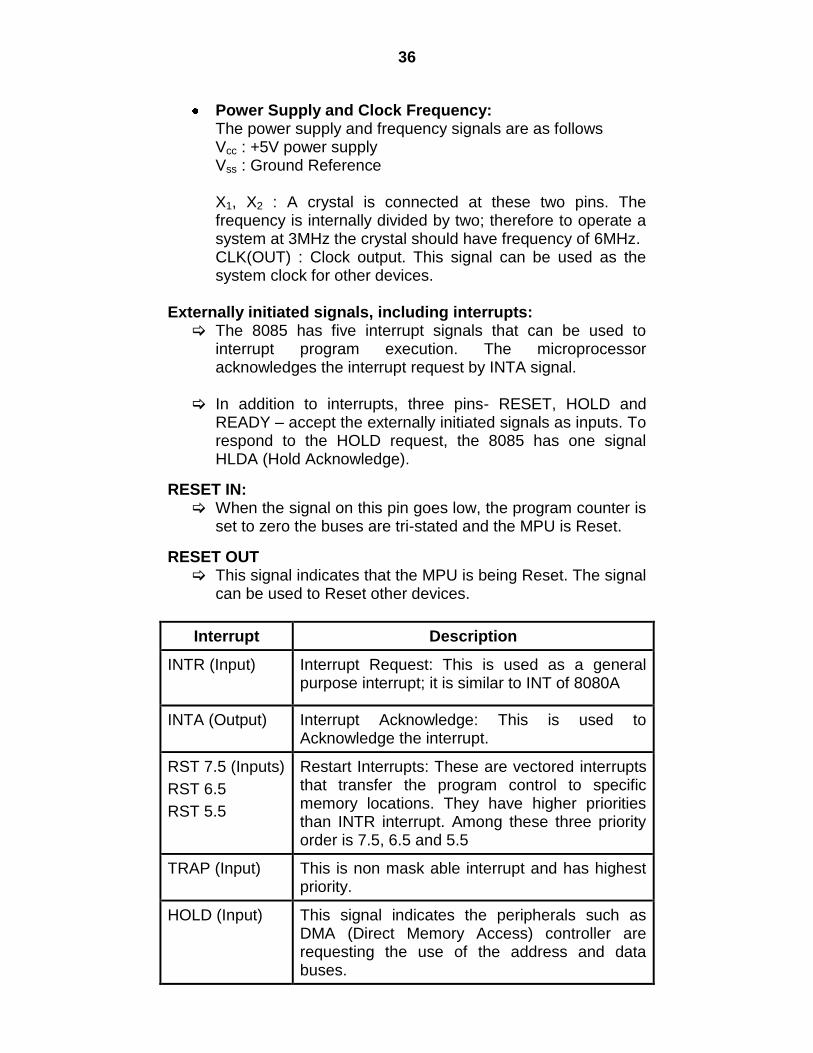
Power Supply and Clock Frequency: The power supply and frequency signals are as follows Vcc : +5V power supply Vss : Ground Reference X1, X2 : A crystal is connected at these two pins. The frequency is internally divided by two; therefore to operate a system at 3MHz the crystal should have frequency of 6MHz. CLK(OUT) : Clock output. This signal can be used as the system clock for other devices.
Externally initiated signals, including interrupts: The 8085 has five interrupt signals that can be used to
interrupt program execution. The microprocessor acknowledges the interrupt request by INTA signal.
In addition to interrupts, three pins- RESET, HOLD and
READY – accept the externally initiated signals as inputs. To respond to the HOLD request, the 8085 has one signal HLDA (Hold Acknowledge).
RESET IN: When the signal on this pin goes low, the program counter is
set to zero the buses are tri-stated and the MPU is Reset.
RESET OUT This signal indicates that the MPU is being Reset. The signal
can be used to Reset other devices.
Interrupt Description
INTR (Input) Interrupt Request: This is used as a general purpose interrupt; it is similar to INT of 8080A
INTA (Output) Interrupt Acknowledge: This is used to Acknowledge the interrupt.
RST 7.5 (Inputs)
RST 6.5
RST 5.5
Restart Interrupts: These are vectored interrupts that transfer the program control to specific memory locations. They have higher priorities than INTR interrupt. Among these three priority order is 7.5, 6.5 and 5.5
TRAP (Input) This is non mask able interrupt and has highest priority.
HOLD (Input) This signal indicates the peripherals such as DMA (Direct Memory Access) controller are requesting the use of the address and data buses.
37
HLDA (Output) Hold Acknowledge: This signal acknowledges the HOLD request.
READY (Input) This signal is used to delay the microprocessor Read or Write cycles until a slow-responding peripheral is ready to send or accept data. When this signal goes low, the microprocessor waits for an integral number of clock cycles until it goes high.
Table 4.2 8085 Interrupts and Externally Initiated Signals
Serial I/O Ports: The 8085 has two signals to implement the serial
transmission: SID (Serial Input Data) and SOD (Serial Output Data).
In serial transmission, data bits are sent over a single line, one bit at a time, such as a transmission over telephone lines.
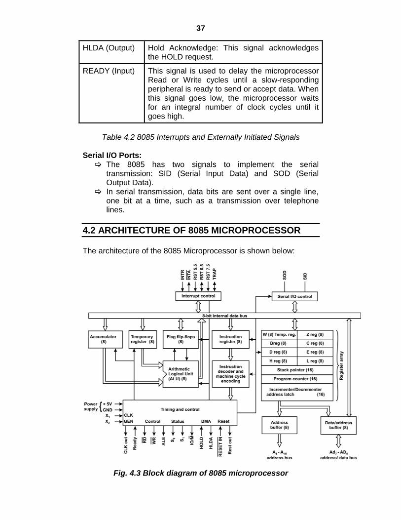
4.2 ARCHITECTURE OF 8085 MICROPROCESSOR
The architecture of the 8085 Microprocessor is shown below:
Fig. 4.3 Block diagram of 8085 microprocessor
38
Control Unit Generates signals within microprocessor to carry out the
instruction, which has been decoded. In reality causes certain connections between blocks of the
microprocessor to be opened or closed, so that data goes where it is required, and so that ALU operations occur.
Arithmetic Logic Unit The ALU performs the actual numerical and logic operation
such as „add‟, „subtract‟, „AND‟, „OR‟, etc. Uses data from memory and from Accumulator to perform
arithmetic. Always stores result of operation in Accumulator.
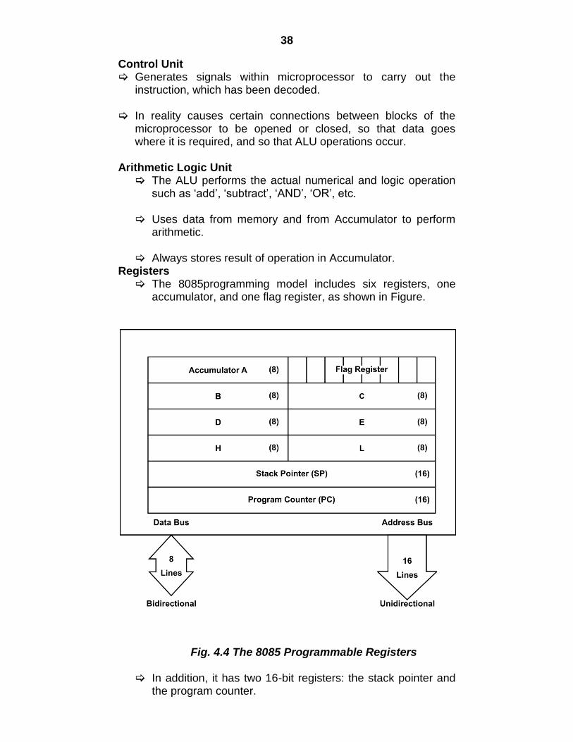
Registers The 8085programming model includes six registers, one
accumulator, and one flag register, as shown in Figure.
Fig. 4.4 The 8085 Programmable Registers
In addition, it has two 16-bit registers: the stack pointer and the program counter.
39
They are described briefly as follows. The 8085/8080A has six general-purpose registers to store
8-bit data; these are identified as B, C, D, E, H and L as shown in the figure.
They can be combined as register pairs - BC, DE, and HL -
to perform some 16-bit operations. The programmer can use these registers to store or copy
data into the registers by using data copy instructions.
Accumulator
The accumulator is an 8-bit register that is a part of arithmetic/logic unit (ALU).
This register is used to store 8-bit data and to perform
arithmetic and logical operations. The result of an operation is stored in the accumulator.
The accumulator is also identified as register A.
Flags The ALU includes five flip-flops, which are set or reset after
an operation according to data conditions of the result in the accumulator and other registers.
They are called Zero (Z), Carry (CY), Sign (S), Parity (P),
and Auxiliary Carry (AC) flags. The most commonly used flags are Zero, Carry, and Sign.
The microprocessor uses these flags to test data conditions.
For example, after an addition of two numbers, if the sum in
the accumulator id larger than eight bits, the flip-flop uses to indicate a carry -- called the Carry flag (CY) -- is set to one.
When an arithmetic operation results in zero, the flip-flop
called the Zero (Z) flag is set to one. The figure shows an 8-bit register, called the flag register,
adjacent to the accumulator.
40
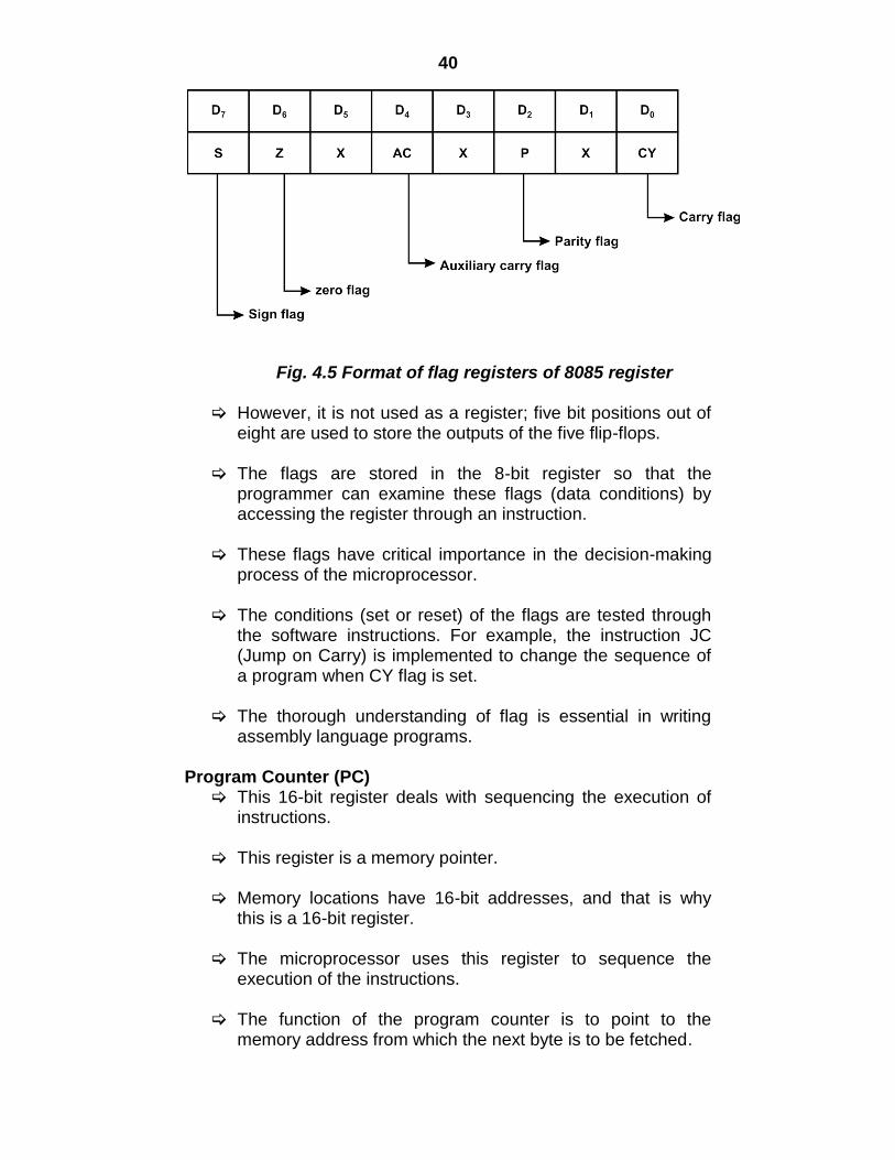
Fig. 4.5 Format of flag registers of 8085 register
However, it is not used as a register; five bit positions out of eight are used to store the outputs of the five flip-flops.
The flags are stored in the 8-bit register so that the
programmer can examine these flags (data conditions) by accessing the register through an instruction.
These flags have critical importance in the decision-making
process of the microprocessor. The conditions (set or reset) of the flags are tested through
the software instructions. For example, the instruction JC (Jump on Carry) is implemented to change the sequence of a program when CY flag is set.
The thorough understanding of flag is essential in writing
assembly language programs. Program Counter (PC) This 16-bit register deals with sequencing the execution of
instructions. This register is a memory pointer.
Memory locations have 16-bit addresses, and that is why
this is a 16-bit register. The microprocessor uses this register to sequence the
execution of the instructions. The function of the program counter is to point to the
memory address from which the next byte is to be fetched.
41
When a byte (machine code) is being fetched, the program counter is incremented by one to point to the next memory location.
Stack Pointer (SP) The stack pointer is also a 16-bit register used as a memory
pointer. It points to a memory location in R/W memory, called the
stack. The beginning of the stack is defined by loading 16-bit
address in the stack pointer. The stack concept is explained in the chapter "Stack and
Subroutines." Instruction Register/Decoder
Temporary store for the current instruction of a program. Latest instruction sent here from memory prior to execution. Decoder then takes instruction and „decodes‟ or interprets
the instruction. Decoded instruction then passed to next stage.
Memory Address Register Holds address, received from PC, of next program
instruction. Feeds the address bus with addresses of location of the
program under execution. Control Generator Generates signals within microprocessor to carry out the
instruction which has been decoded. In reality causes certain connections between blocks of the
uP to be opened or closed, so that data goes where it is required, and so that ALU operations occur.
Register Selector This block controls the use of the register stack in the
example. Just a logic circuit which switches between different registers
in the set will receive instructions from Control Unit.
42
General Purpose Registers Microprocessor requires extra registers for versatility. Can be used to store additional data during a program. More complex processors may have a variety of differently
named registers. 8085 System Bus Typical system uses a number of buses i.e collections of
wires, which transmit binary numbers, one bit per wire in term of voltage levels 0 volt or 5 volt for 0 and 1 respectively.
A typical microprocessor communicates with memory and
other devices input and output using three busses i.e Address bus, Data bus and Control bus.
Address Bus One wire is required for each bit, therefore 16 bits requires
16 wires. Binary number carried by these wires tells memory to open the designated memory location. Binary data can then be store in or taken out from the memory location depending on the control signal.
The Address bus consists of 16 wires, therefore its “width” is
16 bits. A 16 bit binary number allows 216 or 64K different numbers
i.e 0000000000000000 up to 1111111111111111. Because size of memory location is of 8 bit each, each with
a unique address, the size of the address bus determines the size of memory which can be accessed.
To communicate with memory the microprocessor sends an
address on the address bus, e.g 0000000000000011 (3 in decimal), to the memory.
The memory selects location number 3 for reading or writing
data. Address bus is unidirectional, i.e numbers only sent from
microprocessor to memory, not other way. Data Bus Data Bus carries „data‟, in binary form, between
microprocessor and other external devices such as memory or peripherals.
43
Size of data bus is determined by the size of location in memory and data bus size helps determine performance of microprocessor.
The Data Bus is typically of 8 bit, 16 bit or 32 bit and it is bi-
directional. 8085 has 8 bit data bus, therefore 28 combinations of binary
digits are possible. Data bus used to transmit “data”, i.e information, results of
arithmetic, etc between memory and the microprocessor. Therefore larger number has to be broken down into chunks
of 255, this slows microprocessor. Data Bus also carries instructions from memory to the
microprocessor. Size of the bus therefore limits the number of possible
instructions to 256, each specified by a separate number. Control Bus Control bus is unidirectional. How can we tell the address is a memory address or an I/O
port address and read/write data from/to memory or I/O port?
Normally control signal are of following types:
o Memory Read o Memory Write o I/O Read o I/O Write
When Memory Read or I/O Read is active, data is input to the processor.
When Memory Write or I/O Write is active, data is output
from the processor. The control bus signals are defined from the processor‟s
point of view. De-Multiplexing of Address/Data Bus of 8085 In the 8085 microprocessor, the higher order address lines
i.e A8-A15 are directly available, but the lower order address lines are multiplexed with data bus in time sharing.
44
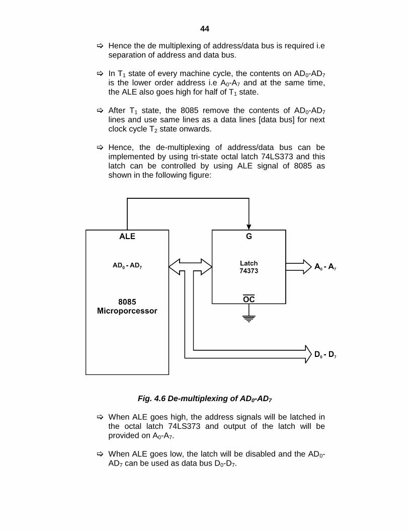
Hence the de multiplexing of address/data bus is required i.e separation of address and data bus.
In T1 state of every machine cycle, the contents on AD0-AD7
is the lower order address i.e A0-A7 and at the same time, the ALE also goes high for half of T1 state.
After T1 state, the 8085 remove the contents of AD0-AD7
lines and use same lines as a data lines [data bus] for next clock cycle T2 state onwards.
Hence, the de-multiplexing of address/data bus can be
implemented by using tri-state octal latch 74LS373 and this latch can be controlled by using ALE signal of 8085 as shown in the following figure:
Fig. 4.6 De-multiplexing of AD0-AD7
When ALE goes high, the address signals will be latched in
the octal latch 74LS373 and output of the latch will be provided on A0-A7.
When ALE goes low, the latch will be disabled and the AD0-
AD7 can be used as data bus D0-D7.
45
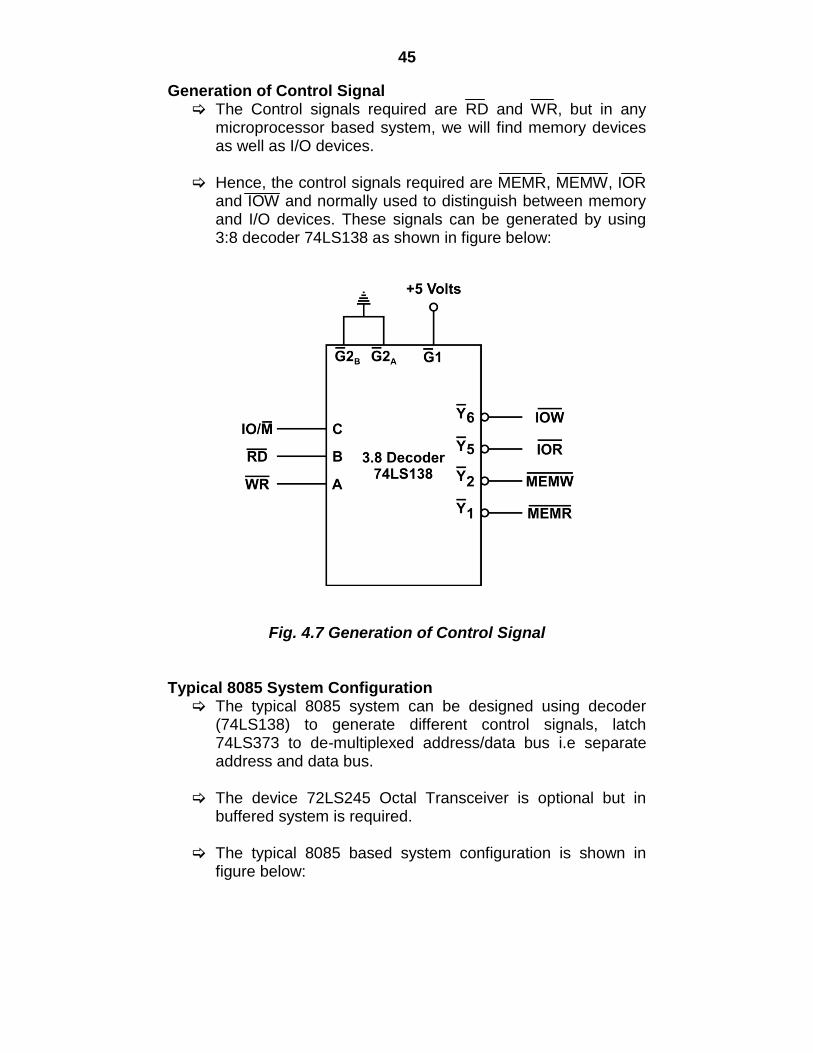
Generation of Control Signal The Control signals required are RD and WR, but in any
microprocessor based system, we will find memory devices as well as I/O devices.
Hence, the control signals required are MEMR, MEMW, IOR
and IOW and normally used to distinguish between memory and I/O devices. These signals can be generated by using 3:8 decoder 74LS138 as shown in figure below:
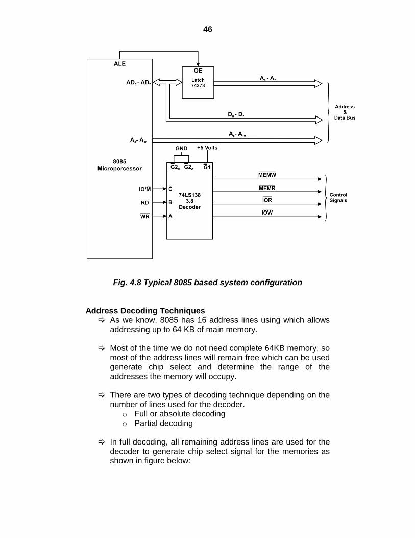
Fig. 4.7 Generation of Control Signal Typical 8085 System Configuration The typical 8085 system can be designed using decoder
(74LS138) to generate different control signals, latch 74LS373 to de-multiplexed address/data bus i.e separate address and data bus.
The device 72LS245 Octal Transceiver is optional but in
buffered system is required. The typical 8085 based system configuration is shown in
figure below:
46
Fig. 4.8 Typical 8085 based system configuration Address Decoding Techniques As we know, 8085 has 16 address lines using which allows
addressing up to 64 KB of main memory. Most of the time we do not need complete 64KB memory, so
most of the address lines will remain free which can be used generate chip select and determine the range of the addresses the memory will occupy.
There are two types of decoding technique depending on the
number of lines used for the decoder. o Full or absolute decoding o Partial decoding
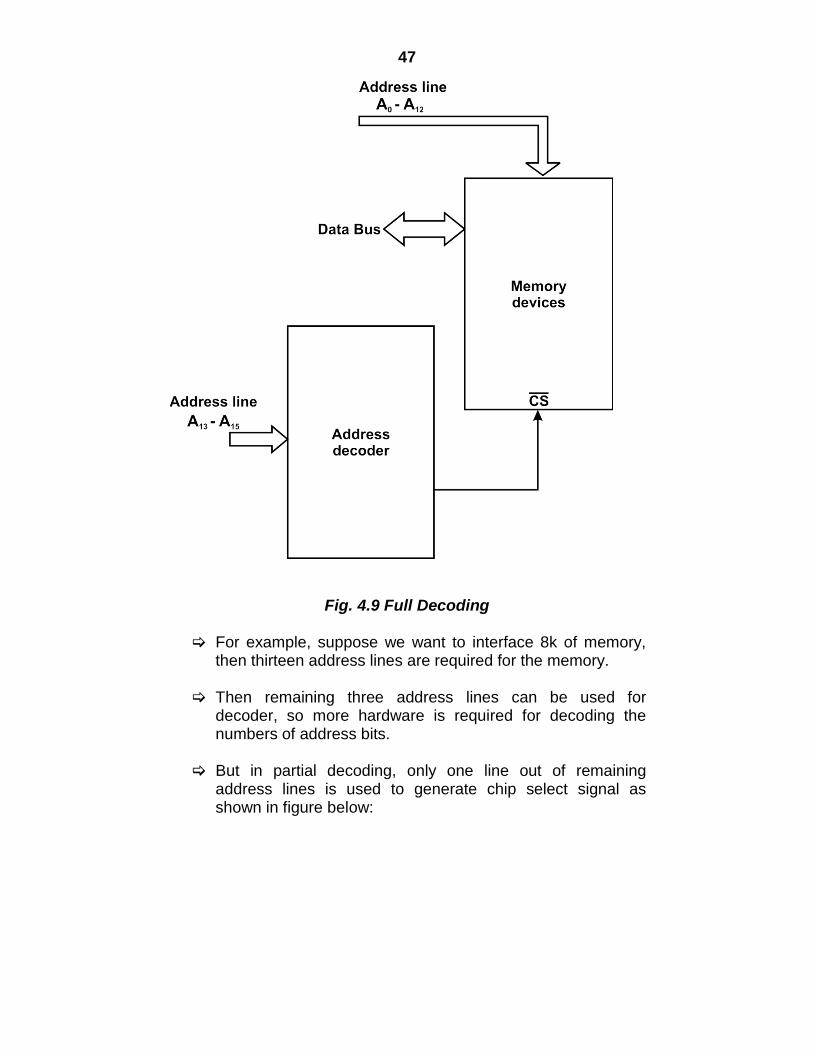
In full decoding, all remaining address lines are used for the decoder to generate chip select signal for the memories as shown in figure below:
47
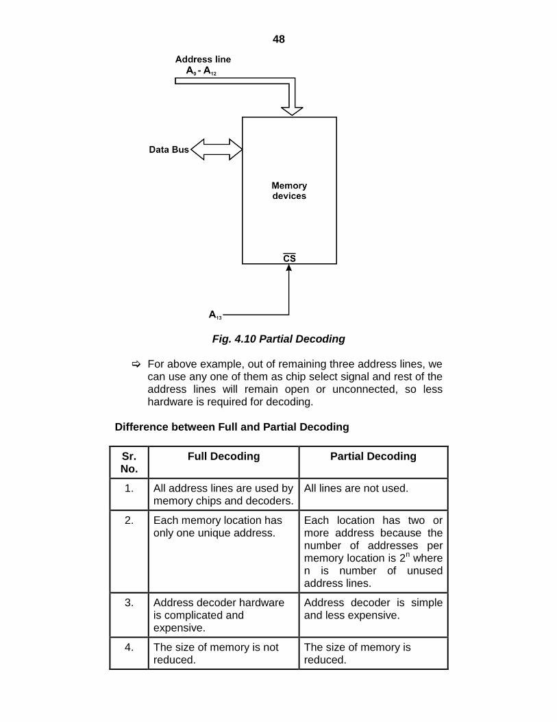
Fig. 4.9 Full Decoding
For example, suppose we want to interface 8k of memory, then thirteen address lines are required for the memory.
Then remaining three address lines can be used for
decoder, so more hardware is required for decoding the numbers of address bits.
But in partial decoding, only one line out of remaining
address lines is used to generate chip select signal as shown in figure below:
48
Fig. 4.10 Partial Decoding
For above example, out of remaining three address lines, we can use any one of them as chip select signal and rest of the address lines will remain open or unconnected, so less hardware is required for decoding.
Difference between Full and Partial Decoding
Sr. No.
Full Decoding Partial Decoding
1. All address lines are used by memory chips and decoders.
All lines are not used.
2. Each memory location has only one unique address.
Each location has two or more address because the number of addresses per memory location is 2n where n is number of unused address lines.
3. Address decoder hardware is complicated and expensive.
Address decoder is simple and less expensive.
4. The size of memory is not reduced.
The size of memory is reduced.
49
Exercise
1. Draw the pin diagram of 8085 microprocessor and explain the various pins.
2. Explain the architecture of 8085 microprocessor with the help of the block diagram.
3. Explain with the help of a diagram various programmable registers of 8085.
4. With the help of a diagram, explain the format of the flag register.
5. Explain Program Counter and Stack Register. 6. Write a short note on 8085 system bus. 7. Explain de multiplexing of address bus of 8085. 8. Write a short note on address decoding techniques. 9. State the difference between full and partial decoding.
References
Computer System Architecture – M. Morris Meno, PHI, 1998
Computer Architecture and Organization - John P Hayes, McGraw Hill, 1998
Digital Computer Fundamentals – Malvino
Digital Computer Fundamentals – Thomas C Bartee, TMG
Computer Organization and Architecture – William Stallings
Microprocessor Architecture and Programming and Applications with the 8085 – R.S. Gaonkar, PRI
50
5
INTERFACING TECHNIQUES
Topics Covered:
5.1 I/O Mapped I/O
5.2 Memory Mapped I/O
5.3 Difference between Memory Mapped I/O and I/O Mapped I/O
5.4 Memory Device
5.5 Chip Select Logic Introduction There are two method of interfacing memory or I/O devices with the microprocessor are as follows:
a) I/O mapped I/O b) Memory mapped I/O
5.1 I/O MAPPED I/O
In this technique, I/O device is treated as a I/Q device and memory as memory.
Each I/Q device uses eight address lines. If eight address lines are used to interface to generate the
address of the I/O port, then 256 input and 256 output devices can be interfaced with the microprocessor.
The address bus of the 8085 microprocessor is 16 bit, so we can either use lower order address lines i.e. A0 – A7 or higher order address lines i.e. A8 – A15 to address I/O devices where the address available on A0 – A7 will be copied on the address lines A8 – A15 .
In I/O mapped I/O, the complete 64 Kbytes of memory can be interfaced as all address lines can be used to address memory locations as the address space is not shared among I/O devices and memory and 256 input and /or output devices.
In this type, the data transfer is possible between accumulator A register and I/O devices only.
Address decoding is simple, as less hardware is required. The separate control signals are used to access I/O devices
and memory such as IOR, IOW for I/O port and MEMR,
51
MEMW for memory hence memory location are protected from the I/O access.
But in this type, arithmetic and logical operation are not possible directly.
Also we cannot use other register for data transfer between I/O device and microprocessor accepts A register.
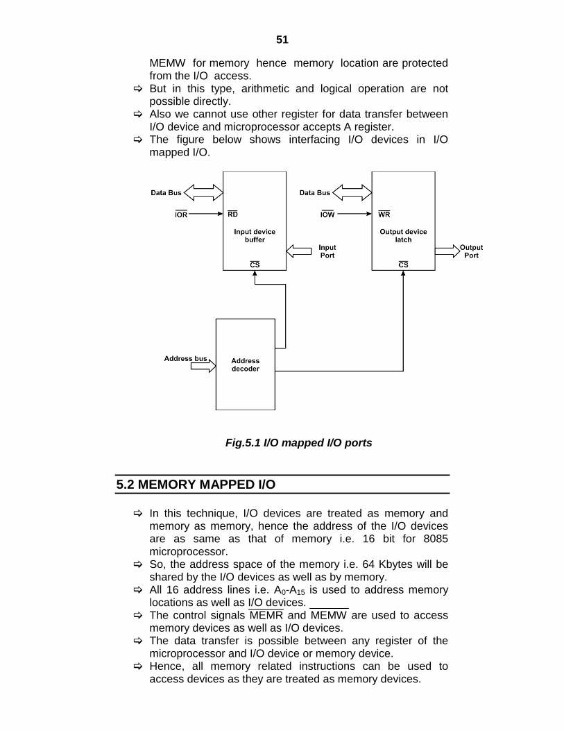
The figure below shows interfacing I/O devices in I/O mapped I/O.
Fig.5.1 I/O mapped I/O ports
5.2 MEMORY MAPPED I/O
In this technique, I/O devices are treated as memory and
memory as memory, hence the address of the I/O devices are as same as that of memory i.e. 16 bit for 8085 microprocessor.
So, the address space of the memory i.e. 64 Kbytes will be shared by the I/O devices as well as by memory.
All 16 address lines i.e. A0-A15 is used to address memory locations as well as I/O devices.
The control signals MEMR and MEMW are used to access memory devices as well as I/O devices.
The data transfer is possible between any register of the microprocessor and I/O device or memory device.
Hence, all memory related instructions can be used to access devices as they are treated as memory devices.
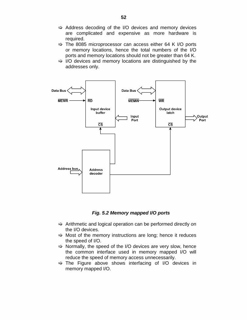
52
Address decoding of the I/O devices and memory devices are complicated and expensive as more hardware is required.
The 8085 microprocessor can access either 64 K I/O ports or memory locations, hence the total numbers of the I/O ports and memory locations should not be greater than 64 K.
I/O devices and memory locations are distinguished by the addresses only.
Fig. 5.2 Memory mapped I/O ports
Arithmetic and logical operation can be performed directly on the I/O devices.
Most of the memory instructions are long; hence it reduces the speed of I/O.
Normally, the speed of the I/O devices are very slow, hence the common interface used in memory mapped I/O will reduce the speed of memory access unnecessarily.
The Figure above shows interfacing of I/O devices in memory mapped I/O.
53
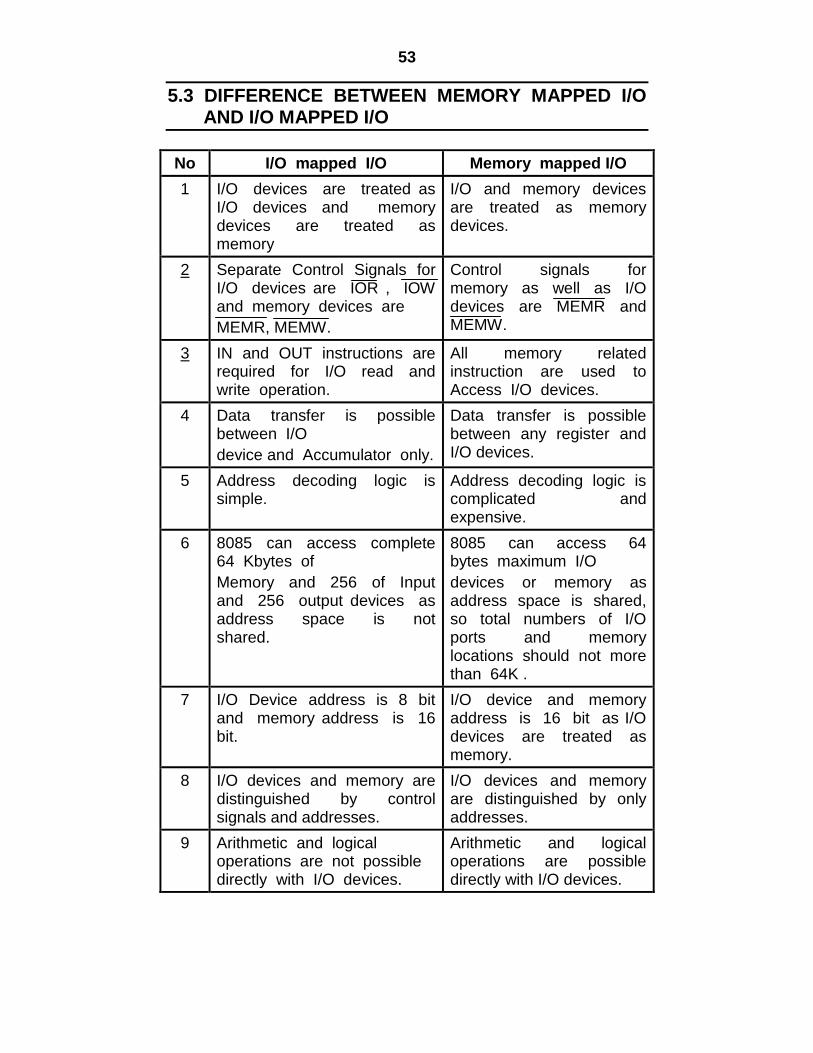
5.3 DIFFERENCE BETWEEN MEMORY MAPPED I/O AND I/O MAPPED I/O
No I/O mapped I/O Memory mapped I/O
1 I/O devices are treated as I/O devices and memory devices are treated as memory
I/O and memory devices are treated as memory devices.
2 Separate Control Signals for I/O devices are IOR , IOW and memory devices are
MEMR, MEMW.
Control signals for memory as well as I/O devices are MEMR and MEMW.
3 IN and OUT instructions are required for I/O read and write operation.
All memory related instruction are used to Access I/O devices.
4 Data transfer is possible between I/O
device and Accumulator only.
Data transfer is possible between any register and I/O devices.
5 Address decoding logic is simple.
Address decoding logic is complicated and expensive.
6 8085 can access complete 64 Kbytes of
Memory and 256 of Input and 256 output devices as address space is not shared.
8085 can access 64 bytes maximum I/O
devices or memory as address space is shared, so total numbers of I/O ports and memory locations should not more than 64K .
7 I/O Device address is 8 bit and memory address is 16 bit.
I/O device and memory address is 16 bit as I/O devices are treated as memory.
8 I/O devices and memory are distinguished by control signals and addresses.
I/O devices and memory are distinguished by only addresses.
9 Arithmetic and logical operations are not possible directly with I/O devices.
Arithmetic and logical operations are possible directly with I/O devices.
54
5.4 MEMORY DEVICE
Memory is the storage device which can be used to store
monitor program, users program or users data. So memory is an important component of the
microprocessor based system, which will allow you to store program and data.
The memory consists of the thousands of memory cells arranged to store data.
Each memory cell is capable of storing 1 bit of the data. Hence, to use memory to store programs or data of user or
system, memory must be interfaced with microprocessor properly, so that it can be accessed while reading or writing data or program from/to it .
In the same way, input and output devices are also required to read or write data out from the microprocessor using input device such as keyboard or output device using console.
So, these devices must be interface properly with the microprocessor so that user can read data from input device and write data to the output device.
Memory Address In computer science, a memory address is a unique identifier
for a memory location at which a CPU or other device can store a piece of data for later retrieval.
In modern byte- addressable computers, each address identifies a single byte of storage; data too large to be stored in a single byte may reside in multiple bytes occupying a sequence of consecutive addresses.
Some microprocessors were designed to be word-addressable, so that the typical storage unit was actually larger than a byte.
Memory Interfacing 1. Each memory chip like RAM, ROM, EPROM, E2PROM and
DRAM have numbers of pins and these pins are used to accept different kinds of signals.
2. Normally every memory chip has pins for address, data, control signals and chip select signals.
Address Pins
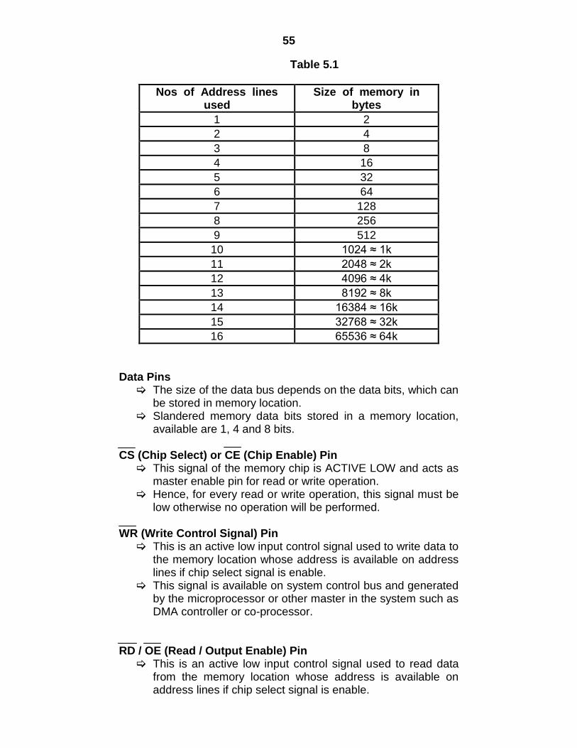
Address pins are used to accept address from the system address bus transmitted by the microprocessor.
The numbers of address pins are depending upon size of the memory as shown in Table below
55
Table 5.1
Nos of Address lines used
Size of memory in bytes
1 2
2 4
3 8
4 16
5 32
6 64
7 128
8 256
9 512
10 1024 ≈ 1k
11 2048 ≈ 2k
12 4096 ≈ 4k
13 8192 ≈ 8k
14 16384 ≈ 16k
15 32768 ≈ 32k
16 65536 ≈ 64k
Data Pins The size of the data bus depends on the data bits, which can
be stored in memory location. Slandered memory data bits stored in a memory location,
available are 1, 4 and 8 bits.
CS (Chip Select) or CE (Chip Enable) Pin This signal of the memory chip is ACTIVE LOW and acts as
master enable pin for read or write operation. Hence, for every read or write operation, this signal must be
low otherwise no operation will be performed. WR (Write Control Signal) Pin This is an active low input control signal used to write data to
the memory location whose address is available on address lines if chip select signal is enable.
This signal is available on system control bus and generated by the microprocessor or other master in the system such as DMA controller or co-processor.
RD / OE (Read / Output Enable) Pin This is an active low input control signal used to read data
from the memory location whose address is available on address lines if chip select signal is enable.
56
This signal is available on system control bus and generated by the microprocessor or other master in the system such as DMA controller or co-processor.
Beside these pin described above, some additional pin also available depending on the type of memory.
For example, Vpp and PGM pins are available in EPROM for programming as in normal condition EPROM is read only memory.
But EPROM can be programmed; the separate EPROM programming hardware is required.
Different Memory IC’s Available are shown in table below Table 5.2
Type of memory
IC number
Memory Sizes Address lines x data lines
EPROM 2716 2K X 8
EPROM 2732 4k x 8
EPROM 2764 8k X 8
SRAM 6116 2k X 8
SRAM 6264 8k x 8
SRAM 2114 1K X 4
5.5 CHIP SELECT LOGIC
Chip select logic can be developed using either combination of different gates such as AND, NAND, NOT etc. or decoders. Using Logic Gates Now take an example of interfacing of 2K of RAM with the
microprocessor 8085, the 8085 is an 8 bit microprocessor. Hence all 8 lines of data bus can be directly connected after de-multiplexing to D0-D7 of the RAM memory. The eleven (11) address lines required to access any memory location within 2k memory, so out of 16 address lines (A0-A15) of 8085 microprocessor, the A0-A10 address lines can be connected directly to generate chip select signal using NAND and NOT gates depending on the addresses required as shown in following figure.
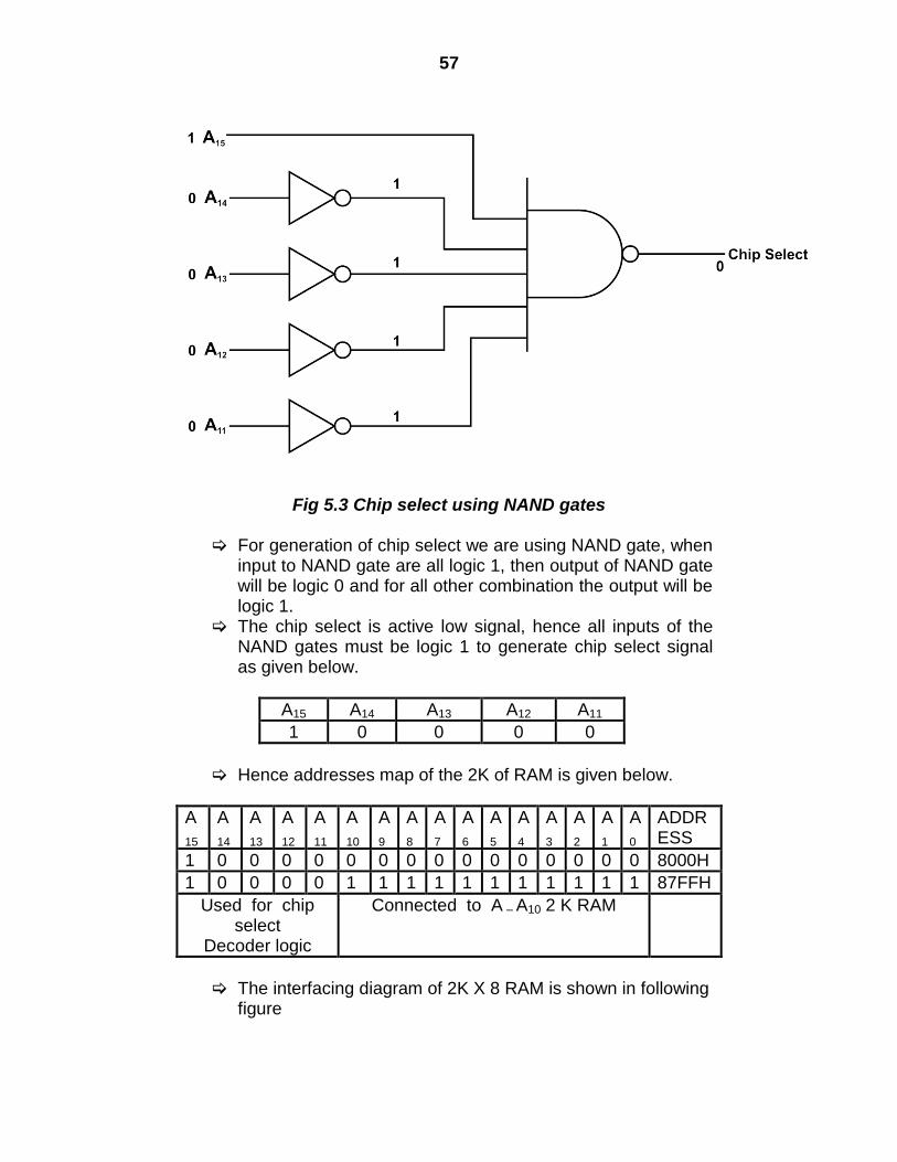
57
Fig 5.3 Chip select using NAND gates
For generation of chip select we are using NAND gate, when input to NAND gate are all logic 1, then output of NAND gate will be logic 0 and for all other combination the output will be logic 1.
The chip select is active low signal, hence all inputs of the NAND gates must be logic 1 to generate chip select signal as given below.
A15 A14 A13 A12 A11
1 0 0 0 0
Hence addresses map of the 2K of RAM is given below.
A
15 A
14 A
13 A
12 A
11 A
10 A
9 A
8 A
7 A
6 A
5 A
4 A
3 A
2 A
1 A
0 ADDRESS
1 0 0 0 0 0 0 0 0 0 0 0 0 0 0 0 8000H
1 0 0 0 0 1 1 1 1 1 1 1 1 1 1 1 87FFH
Used for chip select
Decoder logic
Connected to A – A10 2 K RAM
The interfacing diagram of 2K X 8 RAM is shown in following
figure
58
Fig. 5.4 Interfacing of 2K X 8 RAM
Using Decoder Consider above example of memory interfacing, where
remaining address lines i.e. A11-A15 can be connected to the decoder. Now connect A11, A12, A13 to A, B,C inputs of 3:8 decoder 74LS138 respectively, A14 to G2A and G2B enable pins and at last A15 to G1 pin of 3:8 decoder as shown in following figure.
59
Fig. 5.5 Using decoder
After making the connection as shown above, the address map of 2K RAM will be same as specified above.
60
Fig. 5.6 Interfacing of 2K X 8 RAM using decoder chip select logic
Here, the advantage of using decoder is minimum hardware is required as compared using NAND gates. When we use NAND gates, other logical devices are also required as per requirement as in above examples, NOT gates are used. Hence for numbers of devices, numbers of NAND and other logical devices are required to generate chip select signals.
But when we use decoder like 3:8 (74LS138), we can
generate eight chip select signals using one decoder IC, as it has eight active low output pins. The complete interfacing diagram using decoder to generate chip select signals for 2K of RAM is shown in Fig. 4.6
61
Exercise
1. Explain I/O Mapped I/O with diagram. 2. Explain Memory Mapped I/O with diagram. 3. Differentiate between I/O Mapped I/O and Memory Mapped
I/O. 4. What is a memory device? 5. Explain Memory Interfacing. 6. Explain various data pins. 7. Explain how chip select logic can be used using GATES. 8. Explain how chip select logic can be used using decoders.
References
Computer System Architecture – M. Morris Meno, PHI, 1998
Computer Architecture and Organization - John P Hayes, McGraw Hill, 1998
Digital Computer Fundamentals – Malvino
Digital Computer Fundamentals – Thomas C Bartee, TMG
Computer Organization and Architecture – William Stallings
Microprocessor Architecture and Programming and Applications with the 8085 – R.S. Gaonkar, PRI
62
6 Unit III
8085 MICROPROCESSOR PROGRAMMING MODEL
Topics Covered:
6.1 8085 Programming Model
6.2 Instruction Classification
6.3 Instruction Format
6.4 Overview of 8085 Instruction Set
6.1 8085 PROGRAMMING MODEL
Figure 6.1 8085 programming model
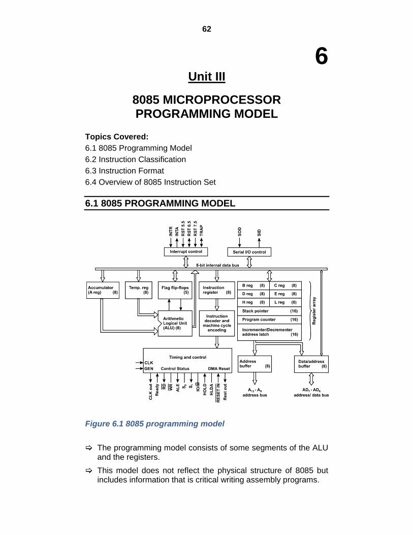
The programming model consists of some segments of the ALU and the registers.
This model does not reflect the physical structure of 8085 but includes information that is critical writing assembly programs.
63
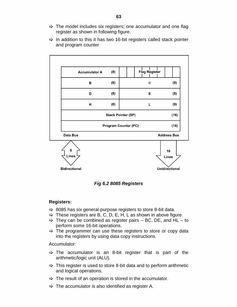
The model includes six registers; one accumulator and one flag register as shown in following figure.
In addition to this it has two 16-bit registers called stack pointer and program counter
Fig 6.2 8085 Registers
Registers:
8085 has six general-purpose registers to store 8-bit data. These registers are B, C, D, E, H, L as shown in above figure. They can be combined as register pairs – BC, DE, and HL – to
perform some 16-bit operations. The programmer can use these registers to store or copy data
into the registers by using data copy instructions.
Accumulator:
The accumulator is an 8-bit register that is part of the arithmetic/logic unit (ALU).
This register is used to store 8-bit data and to perform arithmetic and logical operations.
The result of an operation is stored in the accumulator.
The accumulator is also identified as register A.
64
Flags:
The ALU includes five flip flops, which are set or reset as per the operations results in accumulator and other registers.
They are called Zero(Z) , Carry (CY), Sign(S) , Parity(P) and
Auxiliary carry (AC) flags. The most commonly used flags are Zero, Carry and Sign.
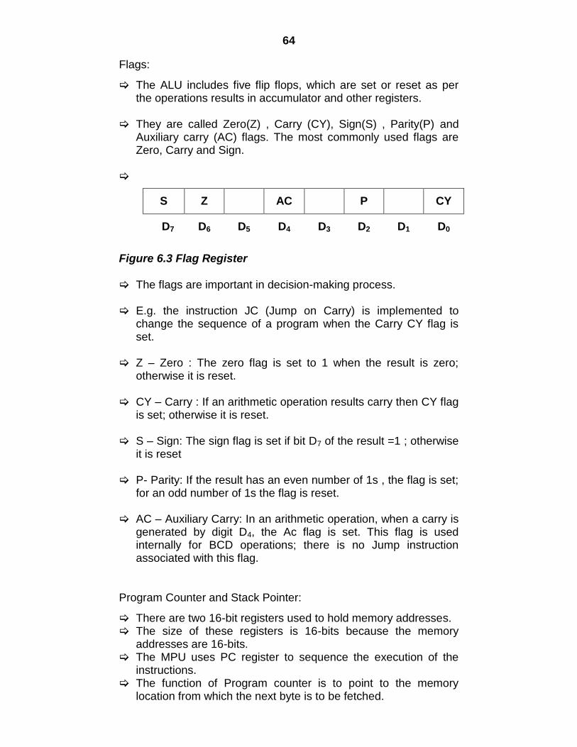
S Z AC P CY
D7 D6 D5 D4 D3 D2 D1 D0
Figure 6.3 Flag Register
The flags are important in decision-making process. E.g. the instruction JC (Jump on Carry) is implemented to
change the sequence of a program when the Carry CY flag is set.
Z – Zero : The zero flag is set to 1 when the result is zero;
otherwise it is reset. CY – Carry : If an arithmetic operation results carry then CY flag
is set; otherwise it is reset. S – Sign: The sign flag is set if bit D7 of the result =1 ; otherwise
it is reset P- Parity: If the result has an even number of 1s , the flag is set;
for an odd number of 1s the flag is reset. AC – Auxiliary Carry: In an arithmetic operation, when a carry is
generated by digit D4, the Ac flag is set. This flag is used internally for BCD operations; there is no Jump instruction associated with this flag.
Program Counter and Stack Pointer:
There are two 16-bit registers used to hold memory addresses. The size of these registers is 16-bits because the memory
addresses are 16-bits. The MPU uses PC register to sequence the execution of the
instructions. The function of Program counter is to point to the memory
location from which the next byte is to be fetched.
65
When a byte(machine code) is fetched the program counter is incremented by one to point to the next memory location.
The stack pointer points to the location in R/W memory. The beginning of the stack is defined by loading 16-bit address in the stack pointer. e.g. Instruction to initialize stack pointer is LXI SP,2400H
6.2 8085 INSTRUCTION CLASSIFICATION
Instruction: An instruction is a binary pattern designed inside
microprocessor to perform a specific function. Entire group of instruction is called instruction set. 8085 instructions are functionally categorized into five types
1) Data transfer (copy) operations 2) Arithmetic operations 3) Logical operations 4) Branching operation 5) Machine control operations
Data transfer (copy) operations: This group of instruction copies data from a location called a
source to another location called destination, without modifying the contents of source.
e.g. a. Copy contents of register B into register D b. Load register B with the data byte 35H c. From memory location 4000H to register B d. From input keyboard to the accumulator Arithmetic operations: Addition: Any 8-bit number, or contents of a register, or the contents of
memory location can be added to the contents of accumulator and sum is stored in the accumulator.
No two other 8-bit registers can be added directly (e.g. Contents of register B cannot be added directly to the contents of C) The instruction DAD is a exception; it adds 16-bit data directly in register pair.
Subtraction: Any 8-bit number, or contents of a register, or the contents of
memory location can be subtracted from the contents of accumulator and the result is stored in the accumulator.
66
The subtraction is performed in 2‟s complement, and the result, if negative, is expressed in 2‟s complement. No two other registers are subtracted directly.
Increment/Decrement: The 8-bit contents of register or memory location can be
incremented or decremented by 1. Similarly, 16-bit contents of register pair can be incremented or
decremented. The increment/decrement differs from addition and subtraction
in such a way that they can be performed on any one the register or in memory location
Logical operations: AND,OR, Exclusive-OR: Any 8-bit number or the contents of a register, or a memory
location can be logically ANDed, ORed, or Exclusive-ORed with the contents of the accumulator. The results are stored in accumulator.
E.g To logically AND the contents of a B register with the
contents of A the instruction is ANA B. Rotate (shift): Each bit in the accumulator is can be shifted either left or right to
the next position. E.g. To rotate left each binary bit of the accumulator instruction is RLC. (Bit D7 is placed in the position of D0 as well as in the Carry flag.)
Compare: Any 8-bit numbers or the contents of a register, or a memory
location can be compared for equality, greater than, or less than, with the contents of accumulator.
E.g. The instruction CPI 32H compare the content of
accumulator with 32H for less than, equal to or greater than. Complement: The content of accumulator can be complemented; all the 0s
are replaced by 1s and all 1s are replaced by 0s. E.g. the instruction is CMA to complement the content of
Accumulator.
67
Branching operation:
Jump: The conditional jumps are an important aspect of the decision-
making process in programming. These instructions test for certain condition (e.g. Zero
/Carry/Sign etc) and alter the program sequence when condition is met. In addition to conditional jump, the instruction set includes unconditional jump. E.g. JMP 2500H
Call, Return and Restart: These instructions change the sequence of program either by
calling a subroutine or returning from a subroutine. The conditional Call and Return instructions also can test
condition flags. Machine control operations: These instructions control machine functions such as Halt,
Interrupt or do nothing.
6.3 INSTRUCTION FORMAT
Instruction word size
8085 instruction set is classified into the following three groups according to word size or byte size.
1) 1-Byte instruction 2) 2-Byte instruction 3) 3-Byte instruction
ONE-Byte Instruction:
A 1-byte instruction includes opcode and operand in the same byte
E.g.
Task Opcode Operand Binary Code
Hex Code
Copy contents of accumulator in reg. C
MOV C, A 0100 1111
4FH
Add contents of reg. B to the contents of accumulator.
ADD B 1000 0000
80H
Invert(Complement) each bit in the accumulator (Implicit operand)
CMA 0010 1111
2FH
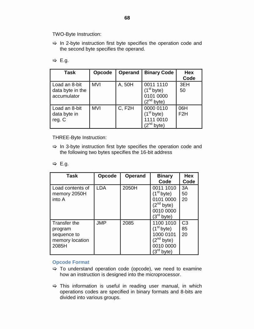
68
TWO-Byte Instruction:
In 2-byte instruction first byte specifies the operation code and the second byte specifies the operand.
E.g.
Task Opcode Operand Binary Code Hex Code
Load an 8-bit data byte in the accumulator
MVI A, 50H 0011 1110 (1st byte) 0101 0000 (2nd byte)
3EH 50
Load an 8-bit data byte in reg. C
MVI C, F2H 0000 0110 (1st byte) 1111 0010 (2nd byte)
06H F2H
THREE-Byte Instruction:
In 3-byte instruction first byte specifies the operation code and the following two bytes specifies the 16-bit address
E.g.
Task Opcode Operand Binary Code
Hex Code
Load contents of memory 2050H into A
LDA 2050H 0011 1010 (1st byte) 0101 0000 (2nd byte) 0010 0000 (3rd byte)
3A 50 20
Transfer the program sequence to memory location 2085H
JMP 2085 1100 1010 (1st byte) 1000 0101 (2nd byte) 0010 0000 (3rd byte)
C3 85 20
Opcode Format
To understand operation code (opcode), we need to examine how an instruction is designed into the microprocessor.
This information is useful in reading user manual, in which
operations codes are specified in binary formats and 8-bits are divided into various groups.
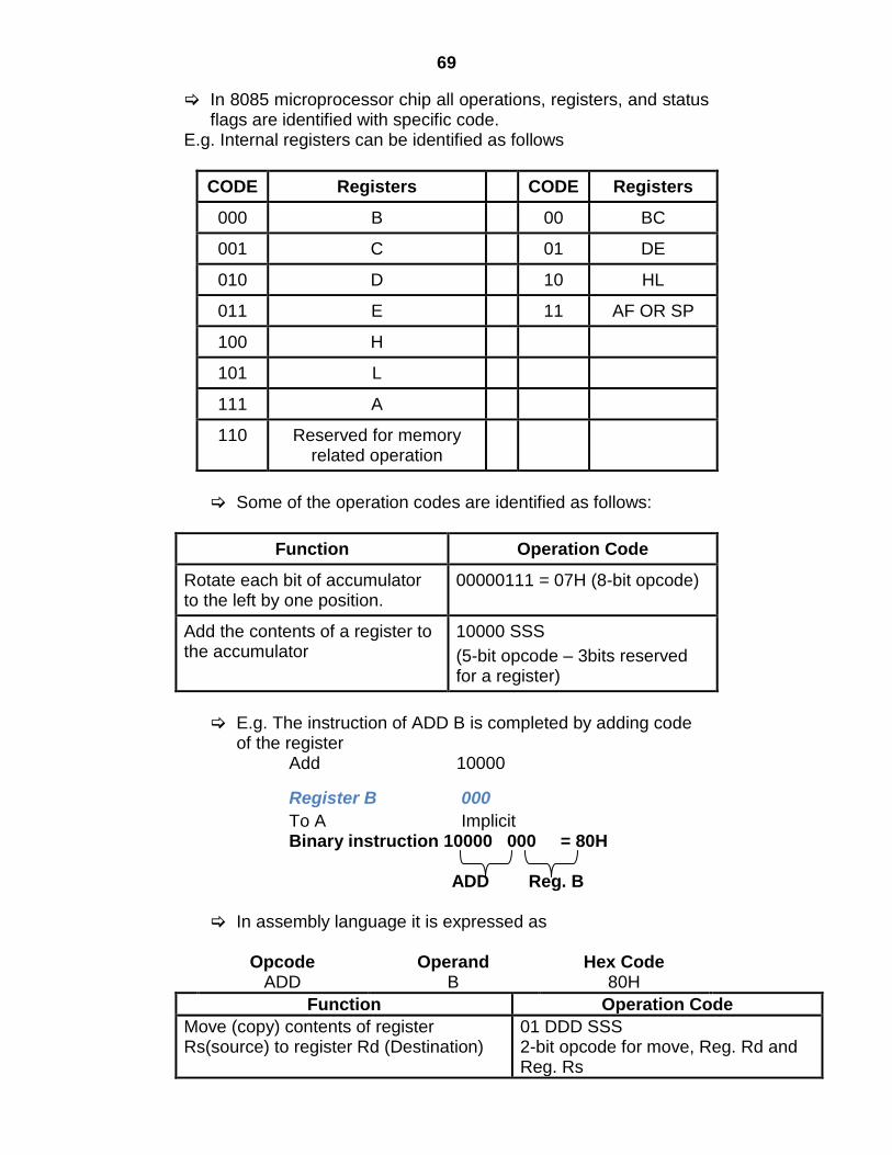
69
In 8085 microprocessor chip all operations, registers, and status flags are identified with specific code.
E.g. Internal registers can be identified as follows
CODE Registers CODE Registers
000 B 00 BC
001 C 01 DE
010 D 10 HL
011 E 11 AF OR SP
100 H
101 L
111 A
110 Reserved for memory related operation
Some of the operation codes are identified as follows:
Function Operation Code
Rotate each bit of accumulator to the left by one position.
00000111 = 07H (8-bit opcode)
Add the contents of a register to the accumulator
10000 SSS
(5-bit opcode – 3bits reserved for a register)
E.g. The instruction of ADD B is completed by adding code
of the register Add 10000
Register B 000
To A Implicit Binary instruction 10000 000 = 80H ADD Reg. B In assembly language it is expressed as
Opcode Operand Hex Code ADD B 80H
Function Operation Code
Move (copy) contents of register Rs(source) to register Rd (Destination)
01 DDD SSS 2-bit opcode for move, Reg. Rd and Reg. Rs
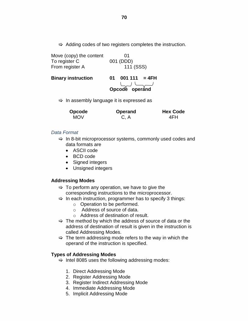
70
Adding codes of two registers completes the instruction.
Move (copy) the content 01 To register C 001 (DDD) From register A 111 (SSS) Binary instruction 01 001 111 = 4FH Opcode operand In assembly language it is expressed as
Opcode Operand Hex Code MOV C, A 4FH
Data Format
In 8-bit microprocessor systems, commonly used codes and data formats are
ASCII code
BCD code
Signed integers
Unsigned integers
Addressing Modes
To perform any operation, we have to give the corresponding instructions to the microprocessor.
In each instruction, programmer has to specify 3 things: o Operation to be performed. o Address of source of data. o Address of destination of result.
The method by which the address of source of data or the address of destination of result is given in the instruction is called Addressing Modes.
The term addressing mode refers to the way in which the operand of the instruction is specified.
Types of Addressing Modes Intel 8085 uses the following addressing modes:
1. Direct Addressing Mode 2. Register Addressing Mode 3. Register Indirect Addressing Mode 4. Immediate Addressing Mode 5. Implicit Addressing Mode
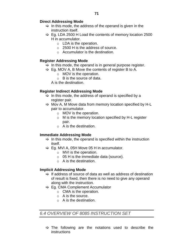
71
Direct Addressing Mode In this mode, the address of the operand is given in the
instruction itself. Eg. LDA 2500 H Load the contents of memory location 2500
H in accumulator. o LDA is the operation. o 2500 H is the address of source. o Accumulator is the destination.
Register Addressing Mode In this mode, the operand is in general purpose register. Eg. MOV A, B Move the contents of register B to A.
o MOV is the operation. o B is the source of data.
A is the destination. Register Indirect Addressing Mode In this mode, the address of operand is specified by a
register pair. Mov A, M Move data from memory location specified by H-L
pair to accumulator. o MOV is the operation. o M is the memory location specified by H-L register
pair. o A is the destination.
Immediate Addressing Mode In this mode, the operand is specified within the instruction
itself. Eg. MVI A, 05H Move 05 H in accumulator.
o MVI is the operation. o 05 H is the immediate data (source). o A is the destination.
Implicit Addressing Mode If address of source of data as well as address of destination
of result is fixed, then there is no need to give any operand along with the instruction.
Eg. CMA Complement Accumulator o CMA is the operation. o A is the source. o A is the destination.
6.4 OVERVIEW OF 8085 INSTRUCTION SET
The following are the notations used to describe the instructions
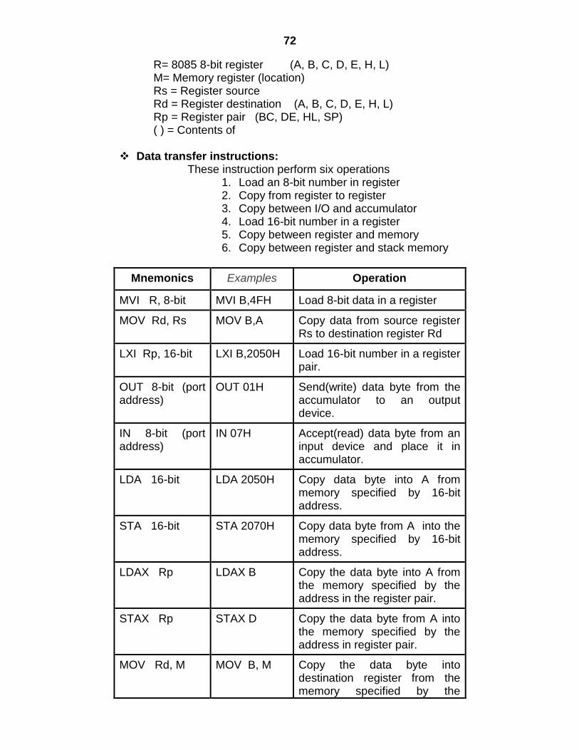
72
R= 8085 8-bit register (A, B, C, D, E, H, L) M= Memory register (location) Rs = Register source Rd = Register destination (A, B, C, D, E, H, L) Rp = Register pair (BC, DE, HL, SP) ( ) = Contents of
Data transfer instructions: These instruction perform six operations
1. Load an 8-bit number in register 2. Copy from register to register 3. Copy between I/O and accumulator 4. Load 16-bit number in a register 5. Copy between register and memory 6. Copy between register and stack memory
Mnemonics Examples Operation
MVI R, 8-bit MVI B,4FH Load 8-bit data in a register
MOV Rd, Rs MOV B,A Copy data from source register Rs to destination register Rd
LXI Rp, 16-bit LXI B,2050H Load 16-bit number in a register pair.
OUT 8-bit (port address)
OUT 01H Send(write) data byte from the accumulator to an output device.
IN 8-bit (port address)
IN 07H Accept(read) data byte from an input device and place it in accumulator.
LDA 16-bit LDA 2050H Copy data byte into A from memory specified by 16-bit address.
STA 16-bit STA 2070H Copy data byte from A into the memory specified by 16-bit address.
LDAX Rp LDAX B Copy the data byte into A from the memory specified by the address in the register pair.
STAX Rp STAX D Copy the data byte from A into the memory specified by the address in register pair.
MOV Rd, M MOV B, M Copy the data byte into destination register from the memory specified by the
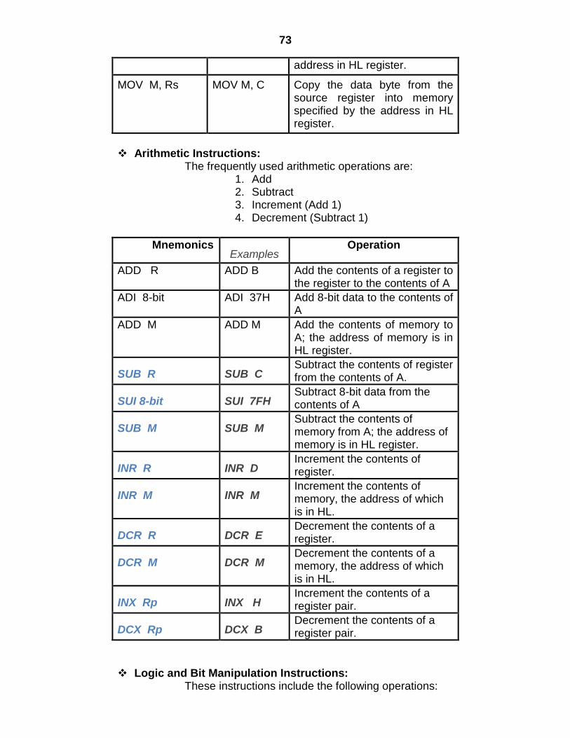
73
address in HL register.
MOV M, Rs MOV M, C Copy the data byte from the source register into memory specified by the address in HL register.
Arithmetic Instructions:
The frequently used arithmetic operations are: 1. Add 2. Subtract 3. Increment (Add 1) 4. Decrement (Subtract 1)
Mnemonics Examples
Operation
ADD R ADD B Add the contents of a register to the register to the contents of A
ADI 8-bit ADI 37H Add 8-bit data to the contents of A
ADD M ADD M Add the contents of memory to A; the address of memory is in HL register.
SUB R SUB C Subtract the contents of register from the contents of A.
SUI 8-bit SUI 7FH Subtract 8-bit data from the contents of A
SUB M SUB M Subtract the contents of memory from A; the address of memory is in HL register.
INR R INR D Increment the contents of register.
INR M INR M Increment the contents of memory, the address of which is in HL.
DCR R DCR E Decrement the contents of a register.
DCR M DCR M Decrement the contents of a memory, the address of which is in HL.
INX Rp INX H Increment the contents of a register pair.
DCX Rp DCX B Decrement the contents of a register pair.
Logic and Bit Manipulation Instructions:
These instructions include the following operations:
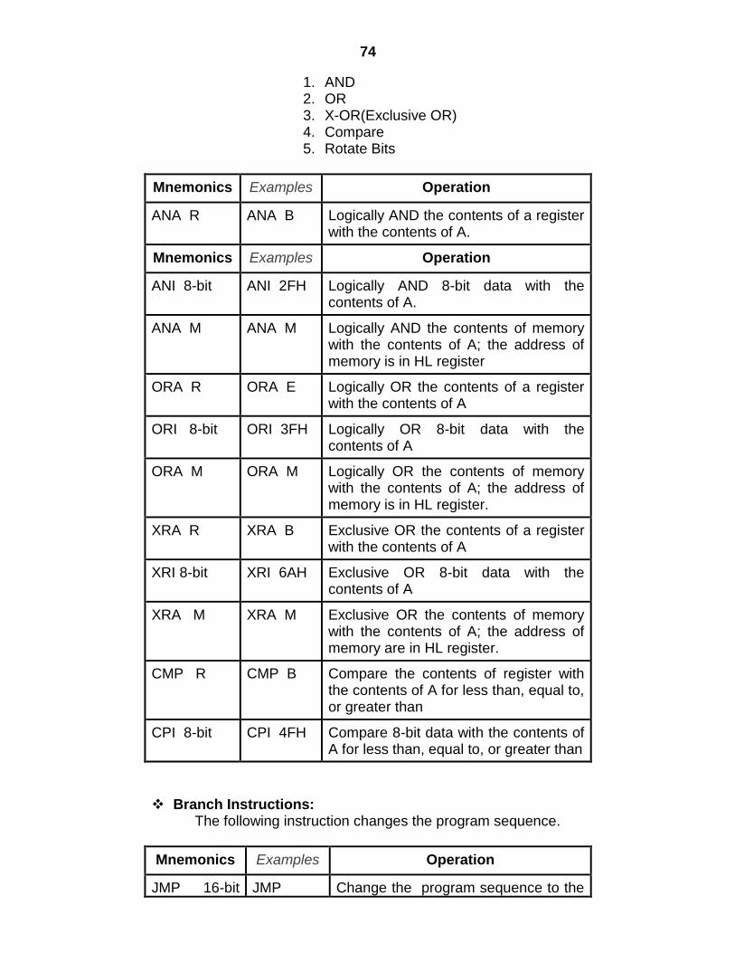
74
1. AND 2. OR 3. X-OR(Exclusive OR) 4. Compare 5. Rotate Bits
Mnemonics Examples Operation
ANA R ANA B Logically AND the contents of a register with the contents of A.
Mnemonics Examples Operation
ANI 8-bit ANI 2FH Logically AND 8-bit data with the contents of A.
ANA M ANA M Logically AND the contents of memory with the contents of A; the address of memory is in HL register
ORA R ORA E Logically OR the contents of a register with the contents of A
ORI 8-bit ORI 3FH Logically OR 8-bit data with the contents of A
ORA M ORA M Logically OR the contents of memory with the contents of A; the address of memory is in HL register.
XRA R XRA B Exclusive OR the contents of a register with the contents of A
XRI 8-bit XRI 6AH Exclusive OR 8-bit data with the contents of A
XRA M XRA M Exclusive OR the contents of memory with the contents of A; the address of memory are in HL register.
CMP R CMP B Compare the contents of register with the contents of A for less than, equal to, or greater than
CPI 8-bit CPI 4FH Compare 8-bit data with the contents of A for less than, equal to, or greater than
Branch Instructions: The following instruction changes the program sequence.
Mnemonics Examples Operation
JMP 16-bit JMP Change the program sequence to the
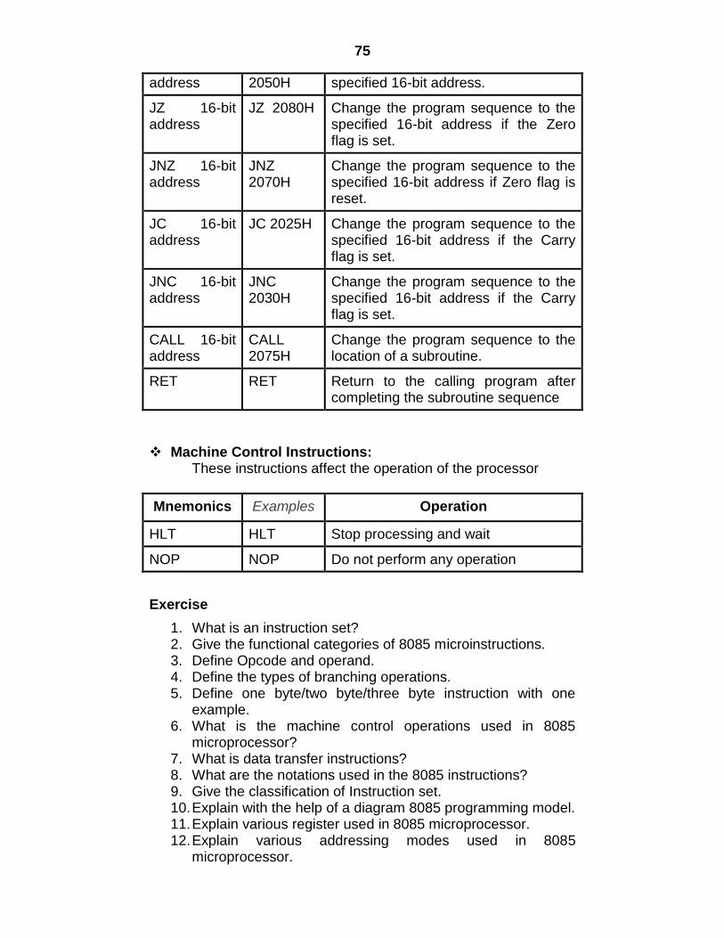
75
address 2050H specified 16-bit address.
JZ 16-bit address
JZ 2080H Change the program sequence to the specified 16-bit address if the Zero flag is set.
JNZ 16-bit address
JNZ 2070H
Change the program sequence to the specified 16-bit address if Zero flag is reset.
JC 16-bit address
JC 2025H Change the program sequence to the specified 16-bit address if the Carry flag is set.
JNC 16-bit address
JNC 2030H
Change the program sequence to the specified 16-bit address if the Carry flag is set.
CALL 16-bit address
CALL 2075H
Change the program sequence to the location of a subroutine.
RET RET Return to the calling program after completing the subroutine sequence
Machine Control Instructions:
These instructions affect the operation of the processor
Mnemonics Examples Operation
HLT HLT Stop processing and wait
NOP NOP Do not perform any operation
Exercise
1. What is an instruction set? 2. Give the functional categories of 8085 microinstructions. 3. Define Opcode and operand. 4. Define the types of branching operations. 5. Define one byte/two byte/three byte instruction with one
example. 6. What is the machine control operations used in 8085
microprocessor? 7. What is data transfer instructions? 8. What are the notations used in the 8085 instructions? 9. Give the classification of Instruction set. 10. Explain with the help of a diagram 8085 programming model. 11. Explain various register used in 8085 microprocessor. 12. Explain various addressing modes used in 8085
microprocessor.
76
References
Computer System Architecture – M. Morris Meno, PHI, 1998
Computer Architecture and Organization - John P Hayes, McGraw Hill, 1998
Digital Computer Fundamentals – Malvino
Digital Computer Fundamentals – Thomas C Bartee, TMG
Computer Organization and Architecture – William Stallings
Microprocessor Architecture and Programming and Applications with the 8085 – R.S. Gaonkar, PRI
77
7
8085 PROGRAMS List of Programs covered: 7.1 To add two 8-bit data
7.2 To add two 8-bit data present in the memory
7.3 To add two 16-bit data
7.4 To subtract two 16-bit data
7.5 To add two 2-digit BCD data
7.6 To add two 4-digit BCD data
7.7 To multiply two numbers of 8-bit data
7.8 To multiply two numbers of 16-bit data
7.9 To divide two numbers of 8-bit data
7.10 To add an array of data
7.11 To search smallest data in the array
7.12 To search largest data in the array
7.13 To sort an array of data in ascending order
7.14 To sort an array of data in descending order
7.15 To find the square root of an 8-bit binary number
7.16 To convert 2 digit BCD to binary number
7.17 To convert 8-bit binary number to BCD
7.18 To convert 8-bit binary to ASCII
7.19 To convert ASCII code to binary value
7.20Transfer a block of data from one location to another
7.1 TO ADD TWO 8-BIT DATA
LDA 0000
MOV B,A
LDA 0001
MVI C,00
ADD B
78
JNC AHEAD
INR C
[LAB1] STA 0002
MOV A,C
STA 0003
HLT
Here, 0000 -> 1st Operand 0001 -> 2nd Operand
0003 -> Sum 0004 -> Carry
7.2 TO ADD TWO 8-BIT DATA PRESENT IN THE MEMORY
LXI H,0000
MVI C,00
MOV A,M
INX H
ADD M
JNC LAB1
INR C
[LAB1] INX H
MOV M,A
INX H
MOV M,C
HLT
Here, 0000 -> 1st Operand 0001 -> 2nd Operand
0003 -> Sum 0004 -> Carry
7.3 TO ADD TWO 16-BIT DATA
LHLD 0000
XCHG
LHLD 0002
XRA A
DAD D
79
JNC LAB1
INR A
[LAB1] SHLD 0004
STA 0006
HLT
Here, 0000 & 0001 -> 1st Operand 0002& 0003 -> 2nd Operand
0004 & 0005 -> Sum 0006 -> Carry
7.4 TO SUBTRACT TWO 16-BIT DATA
LDA 0002
MOV B,A
LDA 0000
SUB B
STA 0004
LDA 0003
MOV B,A
LDA 0001
SBB
STA 0005
HLT
Here, 0000 & 0001 -> 1st Operand 0002& 0003 -> 2nd Operand
0004 & 0005 -> Subtracted Result
7.5 TO ADD TWO 2-DIGIT BCD DATA
LDA 0000
MOV B,A
LDA 0001
MIV C,00
ADD D
DAA
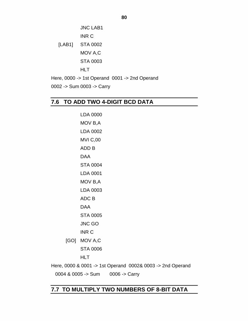
80
JNC LAB1
INR C
[LAB1] STA 0002
MOV A,C
STA 0003
HLT
Here, 0000 -> 1st Operand 0001 -> 2nd Operand
0002 -> Sum 0003 -> Carry
7.6 TO ADD TWO 4-DIGIT BCD DATA
LDA 0000
MOV B,A
LDA 0002
MVI C,00
ADD B
DAA
STA 0004
LDA 0001
MOV B,A
LDA 0003
ADC B
DAA
STA 0005
JNC GO
INR C
[GO] MOV A,C
STA 0006
HLT
Here, 0000 & 0001 -> 1st Operand 0002& 0003 -> 2nd Operand
0004 & 0005 -> Sum 0006 -> Carry
7.7 TO MULTIPLY TWO NUMBERS OF 8-BIT DATA
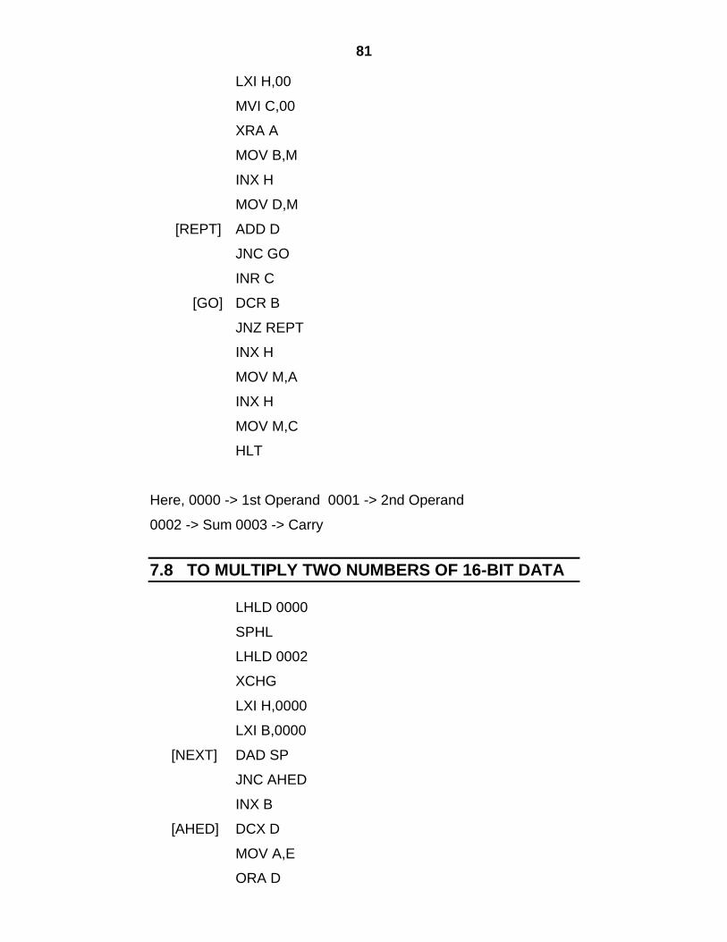
81
LXI H,00
MVI C,00
XRA A
MOV B,M
INX H
MOV D,M
[REPT] ADD D
JNC GO
INR C
[GO] DCR B
JNZ REPT
INX H
MOV M,A
INX H
MOV M,C
HLT
Here, 0000 -> 1st Operand 0001 -> 2nd Operand
0002 -> Sum 0003 -> Carry
7.8 TO MULTIPLY TWO NUMBERS OF 16-BIT DATA
LHLD 0000
SPHL
LHLD 0002
XCHG
LXI H,0000
LXI B,0000
[NEXT] DAD SP
JNC AHED
INX B
[AHED] DCX D
MOV A,E
ORA D
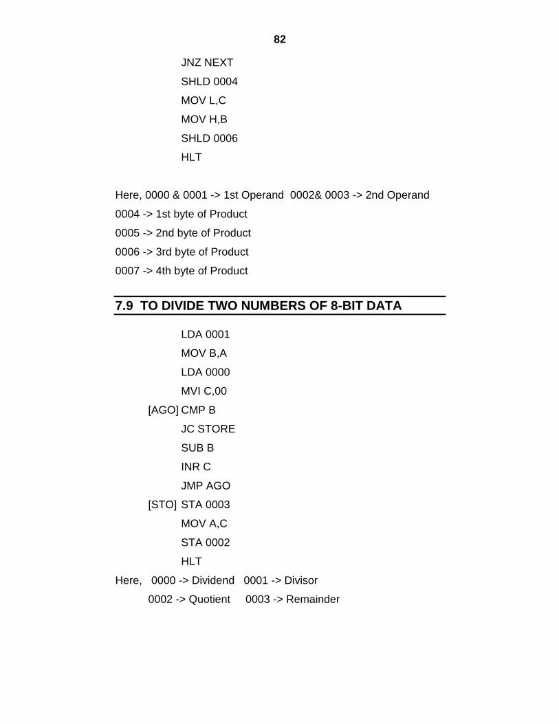
82
JNZ NEXT
SHLD 0004
MOV L,C
MOV H,B
SHLD 0006
HLT
Here, 0000 & 0001 -> 1st Operand 0002& 0003 -> 2nd Operand
0004 -> 1st byte of Product
0005 -> 2nd byte of Product
0006 -> 3rd byte of Product
0007 -> 4th byte of Product
7.9 TO DIVIDE TWO NUMBERS OF 8-BIT DATA
LDA 0001
MOV B,A
LDA 0000
MVI C,00
[AGO] CMP B
JC STORE
SUB B
INR C
JMP AGO
[STO] STA 0003
MOV A,C
STA 0002
HLT
Here, 0000 -> Dividend 0001 -> Divisor
0002 -> Quotient 0003 -> Remainder
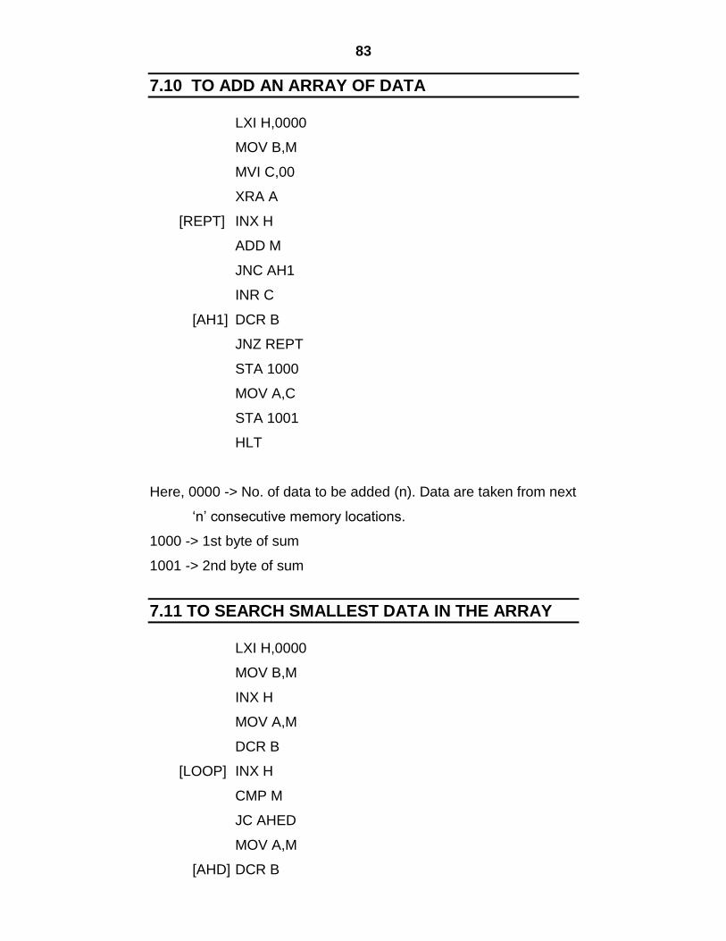
83
7.10 TO ADD AN ARRAY OF DATA
LXI H,0000
MOV B,M
MVI C,00
XRA A
[REPT] INX H
ADD M
JNC AH1
INR C
[AH1] DCR B
JNZ REPT
STA 1000
MOV A,C
STA 1001
HLT
Here, 0000 -> No. of data to be added (n). Data are taken from next
„n‟ consecutive memory locations.
1000 -> 1st byte of sum
1001 -> 2nd byte of sum
7.11 TO SEARCH SMALLEST DATA IN THE ARRAY
LXI H,0000
MOV B,M
INX H
MOV A,M
DCR B
[LOOP] INX H
CMP M
JC AHED
MOV A,M
[AHD] DCR B
84
JNZ LOOP
STA 1000
HLT
Here, 0000 -> No. of data(n). Data are taken from next 'n'
consecutive memory locations.
1000 ->Smallest element
7.12 TO SEARCH LARGEST DATA IN THE ARRAY
LXI H,0000
MOV B,M
INX H
MOV A,M
DCR B
[LOOP] INX H
CMP M
JNC AHED
MOV A,M
[AHED] DCR B
JNZ LOOP
STA 1000
HLT
Here, 0000 -> No. of data(n). Data are taken from next 'n'
consecutive memory locations.
1000 ->Largest element
7.13 TO SORT AN ARRAY OF DATA IN ASCENDING ORDER
LDA 0000
MOV B,A
DCR B
[LOP2] LXI H,1000
MOV C,M
85
DCR C
[LOP1] INX H
MOV A,M
INX H
CMP M
JC AHD1
MOV D,M
MOV M,A
DCX H
MOV M,D
JMP AHED
[AHD1] DCX H
[AHED] DCR C
JNZ LOP1
DCR B
JNZ LOP2
HLT
Here, 0000 -> No. of data (n). Data are taken from next
„n‟ consecutive memory locations.
Sorted data present in the same memory location.
7.14 TO SORT AN ARRAY OF DATA IN DESCENDING ORDER
LDA 0000
MOV B,A
DCR B
[LOP2] LXI H,1000
MOV C,M
DCR C
[LOP1] INX H
MOV A,M
INX H
CMP M
86
JNC AHD1
MOV D,M
MOV M,A
DCX H
MOV M,D
JMP AHED
[AHD1] DCX H
[AHED] DCR C
JNZ LOP1
DCR B
JNZ LOP2
HLT
Here, 0000 -> No. of data (n). Data are taken from next
„n‟ consecutive memory locations.
Sorted data present in the same memory location.
7.15 TO FIND THE SQUARE ROOT OF AN 8-BIT BINARY NUMBER
LDA 0000
MOV B,A
MVI C,02
CALL DIV
[REPT] MOV E,D
MOV A,M
MOV C,D
CALL DIV
MOV A,D
ADD E
MVI C,02
CALL DIV
MOV A,E
CMP D
JNZ REPT
87
STA 0001
HLT
[DIV] MOV D,00
[NEXT] SUB C
INR D
CMP C
JNC NEXT
RET
Here, 0000 -> data 0001 -> Square root of data
7.16 TO CONVERT 2 DIGIT BCD TO BINARY NUMBER
LDA 0000
MOV E,A
ANI F0
RLC
RLC
RLC
RLC
MOV B,A
XRA A
MVI C,0A
[REPT] ADD B
DCR C
JNZ REPT
MOV B,A
MOV A,E
ANI 0F
ADD B
STA 1000
HLT
Here, 0000 -> BCD data 1000 -> Binary data ( result)
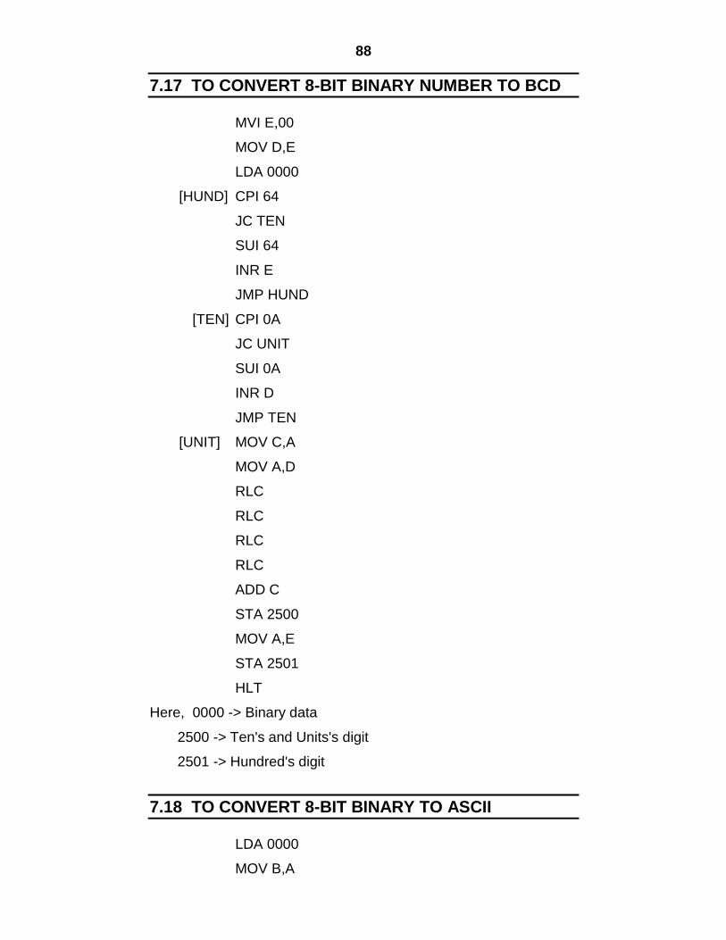
88
7.17 TO CONVERT 8-BIT BINARY NUMBER TO BCD
MVI E,00
MOV D,E
LDA 0000
[HUND] CPI 64
JC TEN
SUI 64
INR E
JMP HUND
[TEN] CPI 0A
JC UNIT
SUI 0A
INR D
JMP TEN
[UNIT] MOV C,A
MOV A,D
RLC
RLC
RLC
RLC
ADD C
STA 2500
MOV A,E
STA 2501
HLT
Here, 0000 -> Binary data
2500 -> Ten's and Units's digit
2501 -> Hundred's digit
7.18 TO CONVERT 8-BIT BINARY TO ASCII
LDA 0000
MOV B,A
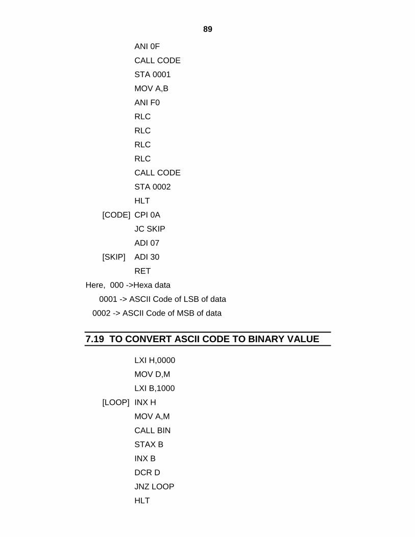
89
ANI 0F
CALL CODE
STA 0001
MOV A,B
ANI F0
RLC
RLC
RLC
RLC
CALL CODE
STA 0002
HLT
[CODE] CPI 0A
JC SKIP
ADI 07
[SKIP] ADI 30
RET
Here, 000 ->Hexa data
0001 -> ASCII Code of LSB of data
0002 -> ASCII Code of MSB of data
7.19 TO CONVERT ASCII CODE TO BINARY VALUE
LXI H,0000
MOV D,M
LXI B,1000
[LOOP] INX H
MOV A,M
CALL BIN
STAX B
INX B
DCR D
JNZ LOOP
HLT
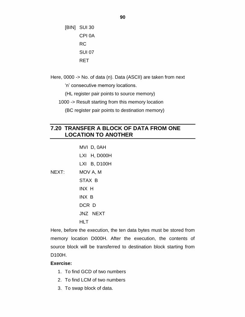
90
[BIN] SUI 30
CPI 0A
RC
SUI 07
RET
Here, 0000 -> No. of data (n). Data (ASCII) are taken from next
„n‟ consecutive memory locations.
(HL register pair points to source memory)
1000 -> Result starting from this memory location
(BC register pair points to destination memory)
7.20 TRANSFER A BLOCK OF DATA FROM ONE LOCATION TO ANOTHER
MVI D, 0AH
LXI H, D000H
LXI B, D100H
NEXT: MOV A, M
STAX B
INX H
INX B
DCR D
JNZ NEXT
HLT
Here, before the execution, the ten data bytes must be stored from
memory location D000H. After the execution, the contents of
source block will be transferred to destination block starting from
D100H.
Exercise:
1. To find GCD of two numbers
2. To find LCM of two numbers
3. To swap block of data.
91
References
Computer System Architecture – M. Morris Meno, PHI, 1998 Computer Architecture and Organization - John P Hayes, McGraw Hill, 1998 Digital Computer Fundamentals – Malvino Digital Computer Fundamentals – Thomas C Bartee, TMG Computer Organization and Architecture – William Stallings Microprocessor Architecture and Programming and Applications with the 8085 – R.S.Gaonkar, PRI
92
8
INTRODUCTION TO MODERN DAY COMPUTER SYSTEMS
Topics Covered:
8.1 Introduction
8.2 Hardware
8.3 Processor
8.4 Bus System
8.5 PCI (Peripheral Component Interface) Bus
8.1 INTRODUCTION
A computer system is made up of both hardware and software.
Software is another term for computer program.
Software controls the computer and makes it do useful work. Without software a computer is useless, like to a car without someone to drive it.
Hardware refers to the physical components that make up a computer system.
These include the computer's processor, memory, monitor, keyboard, mouse, disk drive, printer and so on.
8.2 HARDWARE
The hardware of a computer system is made up of a number of electronic devices connected together. Figures 8.1 and 8.1A are block diagrams of a typical computer system.
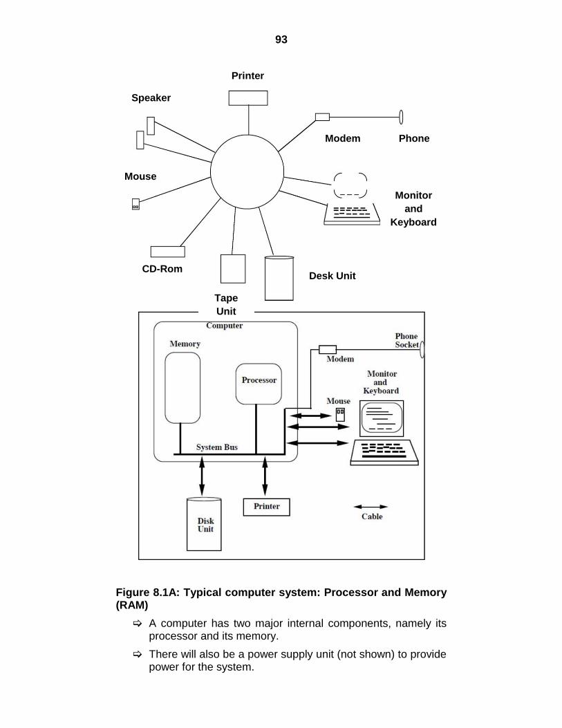
93
Figure 8.1: Typical computer system
Figure 8.1A: Typical computer system: Processor and Memory (RAM)
A computer has two major internal components, namely its processor and its memory.
There will also be a power supply unit (not shown) to provide power for the system.
Printer
Phone
Soket
Modem
Speaker
Mouse
CD-Rom
Tape
Unit
Desk Unit
Monitor
and
Keyboard
94
The term device is used to describe any piece of hardware that we connect to a computer such as a keyboard, monitor, disk drive, printer and so on.
Such devices are also sometimes described as peripheral devices or simply peripherals.
They may be classified as input/output (I/O) devices and storage devices.
As the name suggests, I/O devices are responsible for communicating with the computer, providing input for the computer to process and arranging to display output for computer users.
The keyboard and mouse are commonly used input devices. The monitor is the commonest output device, followed by the printer for hardcopy (permanent) output.
Storage devices are used to store information in a computer system.
The memory is used to store information inside the computer while the computer is switched on.
Disk storage is the commonest form of external storage, followed by the tape storage.
External storage devices can store information indefinitely or more realistically, for some number of years.
A very important component of a computer system is the system bus. This is used to transfer information between all system components.
It is crucial to understand that all information is represented inside a computer system in binary form i.e. using the binary numbers 1 and 0.
The hardware of a computer system has no other way of representing information.
Thus when you press a key on a computer's keyboard, a
binary number (code) which represents the symbol on that key is transmitted to the computer and not the symbol itself, for example, 'A', displayed on the key.
Similarly, when a computer transmits a character to be displayed on the monitor, it is the binary code representing that character that is sent to the monitor.
The monitor hardware takes this binary code and displays the corresponding symbol on the screen.
To reiterate, all information is transmitted and manipulated inside a computer system in the form of binary numbers.
95
A binary digit (1 or 0) is called a bit and a group of 8 bits is called a byte.
When describing storage capacity, the byte and multiples of bytes are the units used. A kilobyte (Kb) is 210 (1024) bytes, a megabyte (Mb) is 220 bytes (1024Kb), a gigabyte (Gb) is 230 bytes (1024Mb) and a terabyte (Tb) is 240 bytes (1024Gb).
When describing transmission speeds, the number of bits per second (bps) is the unit used.
A typical modem can handle speeds of up to 56 Kbps i.e 56 kilo bits per second or approx 56,000 bps.
8.3 THE PROCESSOR
The processor as its name suggests is the unit that does the work of the computer system i.e. it executes computer programs.
Software is composed of instructions, which are executed (obeyed) by the processor.
These instructions tell the processor when and what to read from a keyboard; what to display on a screen; what to store and retrieve from a disk drive and so on.
A computer program is a set of such instructions that carries out a meaningful task. It is worth remembering at this stage that the processor can only perform a limited range of operations.
It can do arithmetic, compare numbers and perform input/output (read information and display or store it).
It is instructive to bear in mind that all computer programs are constructed from sequences of instructions based on such primitive operations.
The processor itself is made up of a number of components such as the arithmetic logic unit (ALU) and the control unit (CU).
The ALU carries out arithmetic operations (e.g. addition and subtraction) and logical operations (e.g. and, or xor) while the CU controls the execution of instructions.
Traditionally, the processor is referred to as the central processing unit or CPU.
With the advent of microprocessors, the term MPU or microprocessor unit is also used.
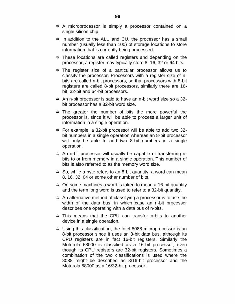
96
A microprocessor is simply a processor contained on a single silicon chip.
In addition to the ALU and CU, the processor has a small number (usually less than 100) of storage locations to store information that is currently being processed.
These locations are called registers and depending on the processor, a register may typically store 8, 16, 32 or 64 bits.
The register size of a particular processor allows us to classify the processor. Processors with a register size of n-bits are called n-bit processors, so that processors with 8-bit registers are called 8-bit processors, similarly there are 16-bit, 32-bit and 64-bit processors.
An n-bit processor is said to have an n-bit word size so a 32-bit processor has a 32-bit word size.
The greater the number of bits the more powerful the processor is, since it will be able to process a larger unit of information in a single operation.
For example, a 32-bit processor will be able to add two 32-bit numbers in a single operation whereas an 8-bit processor will only be able to add two 8-bit numbers in a single operation.
An n-bit processor will usually be capable of transferring n-bits to or from memory in a single operation. This number of bits is also referred to as the memory word size.
So, while a byte refers to an 8-bit quantity, a word can mean 8, 16, 32, 64 or some other number of bits.
On some machines a word is taken to mean a 16-bit quantity and the term long word is used to refer to a 32-bit quantity.
An alternative method of classifying a processor is to use the width of the data bus, in which case an n-bit processor describes one operating with a data bus of n-bits.
This means that the CPU can transfer n-bits to another device in a single operation.
Using this classification, the Intel 8088 microprocessor is an 8-bit processor since it uses an 8-bit data bus, although its CPU registers are in fact 16-bit registers. Similarly the Motorola 68000 is classified as a 16-bit processor, even though its CPU registers are 32-bit registers. Sometimes a combination of the two classifications is used where the 8088 might be described as 8/16-bit processor and the Motorola 68000 as a 16/32-bit processor.
97
The data bus width is very important in a computer system, since it determines the amount of information that can be transferred to or from the CPU, in a single operation.
This means, for example, that the Motorola 68000 would have to transfer two 16-bit items to the CPU to fill a 32-bit register, since the data bus width is 16-bits.
I/O devices and memory operate at very slow speeds compared to the speed of the CPU. As a result, the CPU is frequently delayed by these slower devices, waiting for information to be transferred along the data bus.
So, the more information we can transfer in a single operation, between an I/O devices and the CPU, the less time the CPU will spend waiting for information to process. This in turns means that we should strive to have the data bus as wide as possible.
An important component not shown in Figure 8.1 is the CPU clock.
The clock controls the rate at which activities are carried out by the CPU.
It generate a stream of cycles or ticks and an action can only be carried out on the occurrence of a clock tick.
Obviously, the more cycles per second, the more actions that the CPU can carry out.
The speed of the clock is measured in millions of cycles per second.
One cycle per second is one Hertz (Hz), a kilohertz (KHz) is 1000Hz, a megahertz (MHz) is 1000 KHz and a gigahertz is 1000 MHz. Currently, PCs are being marketed with clock rates range from 2 to 4 GHz and the rate continues to increase.
Bus System
The processor must be able to communicate with all devices.
They are connected together by a communications channel called a bus.
A bus is composed of a set of communication lines or wires.
A simple bus configuration is shown Figure 8.2.
We refer to this bus as the system bus as it connects the various components in a computer system.
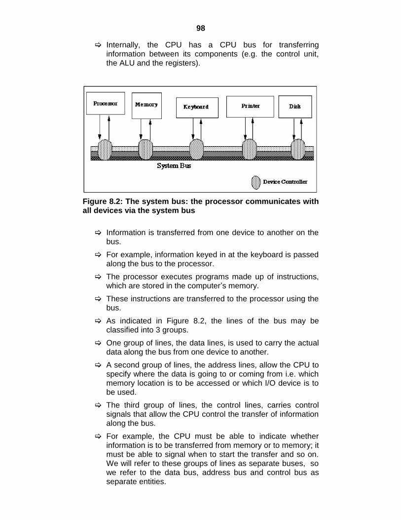
98
Internally, the CPU has a CPU bus for transferring information between its components (e.g. the control unit, the ALU and the registers).
Figure 8.2: The system bus: the processor communicates with all devices via the system bus
Information is transferred from one device to another on the bus.
For example, information keyed in at the keyboard is passed along the bus to the processor.
The processor executes programs made up of instructions, which are stored in the computer‟s memory.
These instructions are transferred to the processor using the bus.
As indicated in Figure 8.2, the lines of the bus may be classified into 3 groups.
One group of lines, the data lines, is used to carry the actual data along the bus from one device to another.
A second group of lines, the address lines, allow the CPU to specify where the data is going to or coming from i.e. which memory location is to be accessed or which I/O device is to be used.
The third group of lines, the control lines, carries control signals that allow the CPU control the transfer of information along the bus.
For example, the CPU must be able to indicate whether information is to be transferred from memory or to memory; it must be able to signal when to start the transfer and so on. We will refer to these groups of lines as separate buses, so we refer to the data bus, address bus and control bus as separate entities.
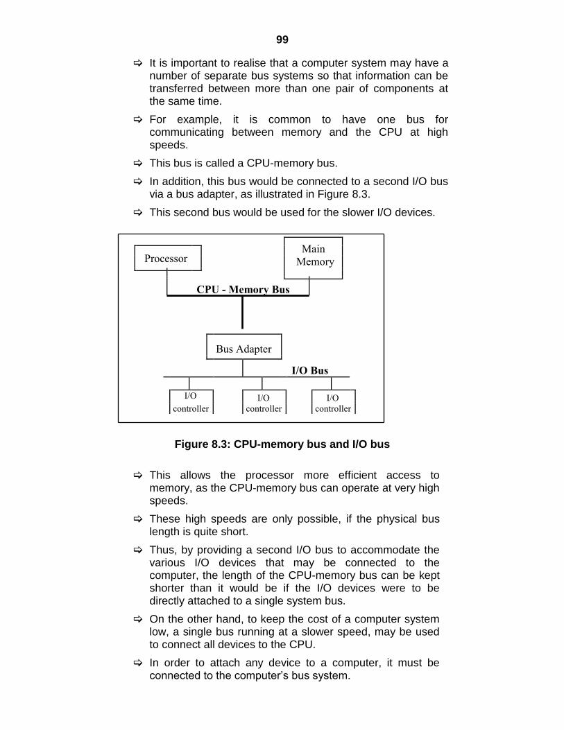
99
It is important to realise that a computer system may have a number of separate bus systems so that information can be transferred between more than one pair of components at the same time.
For example, it is common to have one bus for communicating between memory and the CPU at high speeds.
This bus is called a CPU-memory bus.
In addition, this bus would be connected to a second I/O bus via a bus adapter, as illustrated in Figure 8.3.
This second bus would be used for the slower I/O devices.
Main
Processor
Memory
CPU - Memory Bus
Bus Adapter
I/O Bus
I/O I/O I/O
controller
controller controller
Figure 8.3: CPU-memory bus and I/O bus
This allows the processor more efficient access to memory, as the CPU-memory bus can operate at very high speeds.
These high speeds are only possible, if the physical bus length is quite short.
Thus, by providing a second I/O bus to accommodate the various I/O devices that may be connected to the computer, the length of the CPU-memory bus can be kept shorter than it would be if the I/O devices were to be directly attached to a single system bus.
On the other hand, to keep the cost of a computer system low, a single bus running at a slower speed, may be used to connect all devices to the CPU.
In order to attach any device to a computer, it must be connected to the computer‟s bus system.
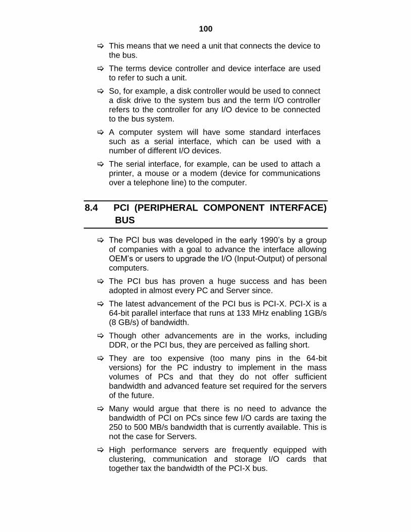
100
This means that we need a unit that connects the device to the bus.
The terms device controller and device interface are used to refer to such a unit.
So, for example, a disk controller would be used to connect a disk drive to the system bus and the term I/O controller refers to the controller for any I/O device to be connected to the bus system.
A computer system will have some standard interfaces such as a serial interface, which can be used with a number of different I/O devices.
The serial interface, for example, can be used to attach a printer, a mouse or a modem (device for communications over a telephone line) to the computer.
8.4 PCI (PERIPHERAL COMPONENT INTERFACE)
BUS
The PCI bus was developed in the early 1990‟s by a group of companies with a goal to advance the interface allowing OEM‟s or users to upgrade the I/O (Input-Output) of personal computers.
The PCI bus has proven a huge success and has been adopted in almost every PC and Server since.
The latest advancement of the PCI bus is PCI-X. PCI-X is a 64-bit parallel interface that runs at 133 MHz enabling 1GB/s (8 GB/s) of bandwidth.
Though other advancements are in the works, including DDR, or the PCI bus, they are perceived as falling short.
They are too expensive (too many pins in the 64-bit versions) for the PC industry to implement in the mass volumes of PCs and that they do not offer sufficient bandwidth and advanced feature set required for the servers of the future.
Many would argue that there is no need to advance the bandwidth of PCI on PCs since few I/O cards are taxing the 250 to 500 MB/s bandwidth that is currently available. This is not the case for Servers.
High performance servers are frequently equipped with clustering, communication and storage I/O cards that together tax the bandwidth of the PCI-X bus.
101
Another key limitation of PCI-X is that it can support only one slot per controller, which means that multiple controllers (and their expense) are needed on each server.
Features of PCI Bus
Speed: The basic PCI protocol can transfer up to 132 Mbytes per second, well over an order of magnitude faster than other buses.
Configurability: PCI offers the ability to configure a system automatically, relieving the user of the task of system configuration.
Multiple Masters: Prior to PCI, most buses supported only one “master”, the processor. High bandwidth devices could have direct access to memory through a mechanism called DMA (Direct Memory Access) but devices, in general, could not talk to each other. In PCI, any device has the potential to take control of the bus and initiate transactions with any other device.
Reliability: “Hot Plug” and “Hot Swap”, defined respectively for PCI and compact PCI, offer the ability to replace modules without disrupting a system‟s operation. This sustainability reduces MTTR (Mean Time to Repair) to yield the necessary degree of up-time required of mission-critical systems such as the telephone network.
The transfer protocol is optimized around transferring blocks of data. A single transfer is just a block transfer with a length of one.
Although PCI is officially processor-independent, it inevitably reflects its origins with Intel and its primary application in the PC architecture.
PCI implements plug and play configurability. Every device in the system is automatically configured each time the system is turned on. The configuration protocol supports up to 256 devices in a system.
The electrical specifications emphasize low power use including support for both 3.3 and 5 volt signaling environments. PCI is a “green” architecture.
System with PCI Bus
The system with PCI is shown in figure below.
The “PCI Bridge” connects between the CPU/Cache/Memory sub system and PCI bus.
It provides low latency path for the CPU to access any PCI device mapped into the I/O or memory space.
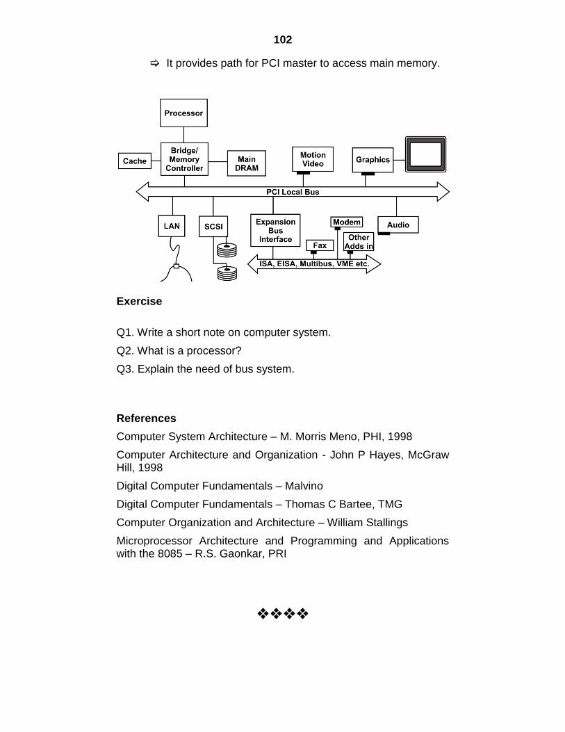
102
It provides path for PCI master to access main memory.
Exercise
Q1. Write a short note on computer system.
Q2. What is a processor?
Q3. Explain the need of bus system.
References
Computer System Architecture – M. Morris Meno, PHI, 1998
Computer Architecture and Organization - John P Hayes, McGraw Hill, 1998
Digital Computer Fundamentals – Malvino
Digital Computer Fundamentals – Thomas C Bartee, TMG
Computer Organization and Architecture – William Stallings
Microprocessor Architecture and Programming and Applications with the 8085 – R.S. Gaonkar, PRI
103
9
COMPUTER MEMORY
Topics Covered:
9.1 Memory
9.2 Cache Memory
9.3 Computer Memory System Overview
9.4 Cache Memory Principles
9.5 Cache Mapping
9.1 MEMORY
Memory is used to store the information (programs and data) that the computer is currently using.
It is sometimes called main or primary memory. One form of memory is called RAM -random access
memory. This means that any location in memory may be accessed in the same amount of time as any other location.
Memory access means one of two things, either the CPU is reading from a memory location or the CPU is writing to a memory location.
When the CPU reads from a memory location, the contents of the memory location are copied to a CPU register.
When the CPU writes to a memory location, the CPU copies the contents of a CPU register to the memory location, overwriting the previous contents of the location.
The CPU cannot carry out any other operations on memory locations.
RAM is a form of short term or volatile memory. Information stored in short term storage is lost when the
computer is switched off (or when power fails). There is therefore a requirement for permanent or long term
storage which is also referred to as secondary storage or auxiliary storage.
This role is fulfilled by disk and tape storage. RAM consists of a large number of storage locations or cells,
each one capable of storing a small amount of information typically a single byte. These cells are numbered or addressed starting at zero, up to some maximum number
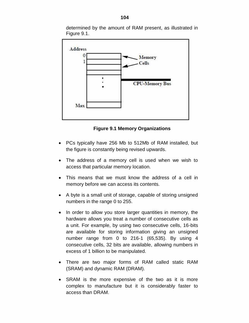
104
determined by the amount of RAM present, as illustrated in Figure 9.1.
Figure 9.1 Memory Organizations
PCs typically have 256 Mb to 512Mb of RAM installed, but
the figure is constantly being revised upwards.
The address of a memory cell is used when we wish to
access that particular memory location.
This means that we must know the address of a cell in
memory before we can access its contents.
A byte is a small unit of storage, capable of storing unsigned
numbers in the range 0 to 255.
In order to allow you store larger quantities in memory, the
hardware allows you treat a number of consecutive cells as
a unit. For example, by using two consecutive cells, 16-bits
are available for storing information giving an unsigned
number range from 0 to 216-1 (65,535). By using 4
consecutive cells, 32 bits are available, allowing numbers in
excess of 1 billion to be manipulated.
There are two major forms of RAM called static RAM
(SRAM) and dynamic RAM (DRAM).
SRAM is the more expensive of the two as it is more
complex to manufacture but it is considerably faster to
access than DRAM.
105
DRAM has an access time in the range of 20-60
nanoseconds upwards, while SRAM access times range
from 4 or 5 nanoseconds to 20 nanoseconds.
It is not uncommon for a computer system to have a small
amount of SRAM and a larger volume of DRAM making up
its total RAM capacity.
The SRAM is used to construct a cache memory which
stores frequently accessed information and so speed up
memory access for the system.
There are other forms of primary memory such as ROM,
PROM, EPROM EEPROM and flash memory.
ROM (Read Only Memory) is the same as RAM in so far as
any location can be read from at random, but it cannot be
written to.
ROM is pre-programmed by the manufacturer and its
contents cannot be changed, hence its name read only.
This means that ROM is a form of permanent storage.
However, since the user cannot store information in ROM, its
usefulness is restricted.
ROM is typically used to store programs and data that are
required to start up (boot) a computer system.
When a computer is powered on, its RAM will contain no
useful information, but the processor is designed to run
programs that it finds in memory.
One major use of ROM is to store the initial program used by
the processor when the machine is started.
Another use of ROM in personal computers, is to store
operating systems subprograms for carrying out I/O and
other activities.
The term firmware is used for the combination of ROM and
the software stored on it.
PROM stands for programmable ROM which means that the
memory chip manufacturer provides a form of ROM that can
be programmed via the use of a special hardware device.
106
This allows computer system designers place their own
programs on the PROM chip. If their programs do not
operate correctly, the designer can program another PROM
chip, as opposed to getting the memory manufacturer to do
it, as is the case when a designer uses ROM.
EPROM is a form of ROM that is erasable which means that
the contents of the EPROM chip can be erased in their
entirety and the chip can be reprogrammed (a limited
number of times).
As in the case of PROM, EPROM can only be programmed
and erased (via exposure to ultra violet light) by a special
hardware device, outside the computer system.
EEPROM is electrically erasable PROM. EEPROM can be
erased inside a computer system using an electrical current.
Its major advantage is that it does not have to be removed
from the computer system.
9.2 CACHE MEMORY
Computer memory is organized into a hierarchy.
At the highest level (closest to the processor) are the processor registers.
Next comes one or more levels of cache.
When multiple levels are used, they are denoted L1, L2, etc…
Next comes main memory, which is usually made out of a dynamic random-access memory (DRAM).
All of these are considered internal to the computer system.
The hierarchy continues with external memory, with the next level typically being a fixed hard disk, and one or more levels below that consisting of removable media such as ZIP cartridges, optical disks, and tape.
As one goes down the memory hierarchy, one finds decreasing cost/bit, increasing capacity, and slower access time.
It would be nice to use only the fastest memory, but because that is the most expensive memory, we trade off access time and cost by using more of the slower memory.
The trick is to organize the data and programs in memory so
107
that the memory words needed are usually in the fastest memory.
In general, it is likely that most future accesses to main memory by the processor will be to locations recently accesses.
So the cache automatically retains a copy of some of the recently used words from the DRAM.
If the cache is designed properly, then most of the time the processor will request memory words that are already in the cache.
9.3 COMPUTER MEMORY SYSTEM OVERVIEW
Characteristics of Memory Systems
Location
Processor
Internal – main memory
External – secondary memory
Capacity
Word size – natural unit or organization
Number of words – number of bytes
Unit of Transfer
Internal
o Usually governed by bus width
External
o Usually a block which is much larger than a word
Addressable unit
o Smallest location which can be uniquely addressed
o Cluster on external disk
Access Methods
Sequential – tape
o Start at the beginning and read through in order
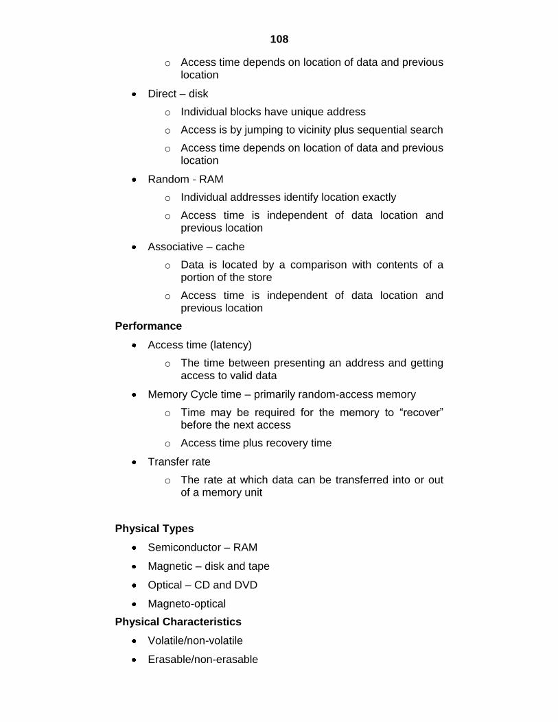
108
o Access time depends on location of data and previous location
Direct – disk
o Individual blocks have unique address
o Access is by jumping to vicinity plus sequential search
o Access time depends on location of data and previous location
Random - RAM
o Individual addresses identify location exactly
o Access time is independent of data location and previous location
Associative – cache
o Data is located by a comparison with contents of a portion of the store
o Access time is independent of data location and previous location
Performance
Access time (latency)
o The time between presenting an address and getting access to valid data
Memory Cycle time – primarily random-access memory
o Time may be required for the memory to “recover” before the next access
o Access time plus recovery time
Transfer rate
o The rate at which data can be transferred into or out of a memory unit
Physical Types
Semiconductor – RAM
Magnetic – disk and tape
Optical – CD and DVD
Magneto-optical
Physical Characteristics
Volatile/non-volatile
Erasable/non-erasable
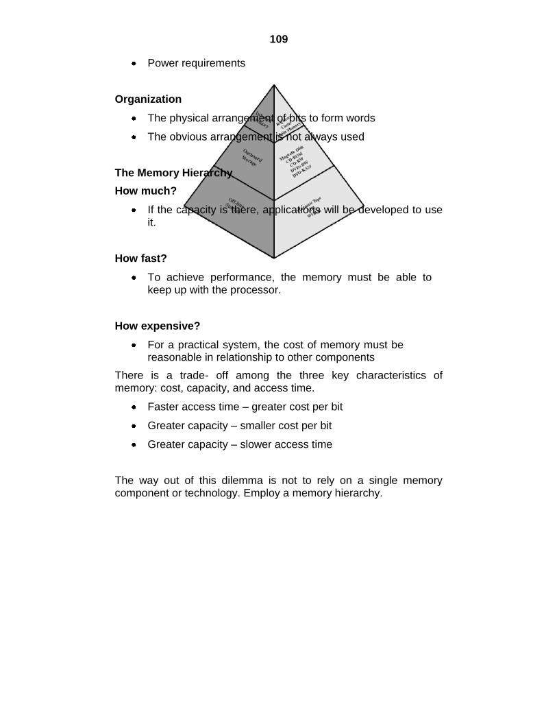
109
Power requirements
Organization
The physical arrangement of bits to form words
The obvious arrangement is not always used
The Memory Hierarchy
How much?
If the capacity is there, applications will be developed to use it.
How fast?
To achieve performance, the memory must be able to keep up with the processor.
How expensive?
For a practical system, the cost of memory must be reasonable in relationship to other components
There is a trade- off among the three key characteristics of memory: cost, capacity, and access time.
Faster access time – greater cost per bit
Greater capacity – smaller cost per bit
Greater capacity – slower access time
The way out of this dilemma is not to rely on a single memory component or technology. Employ a memory hierarchy.
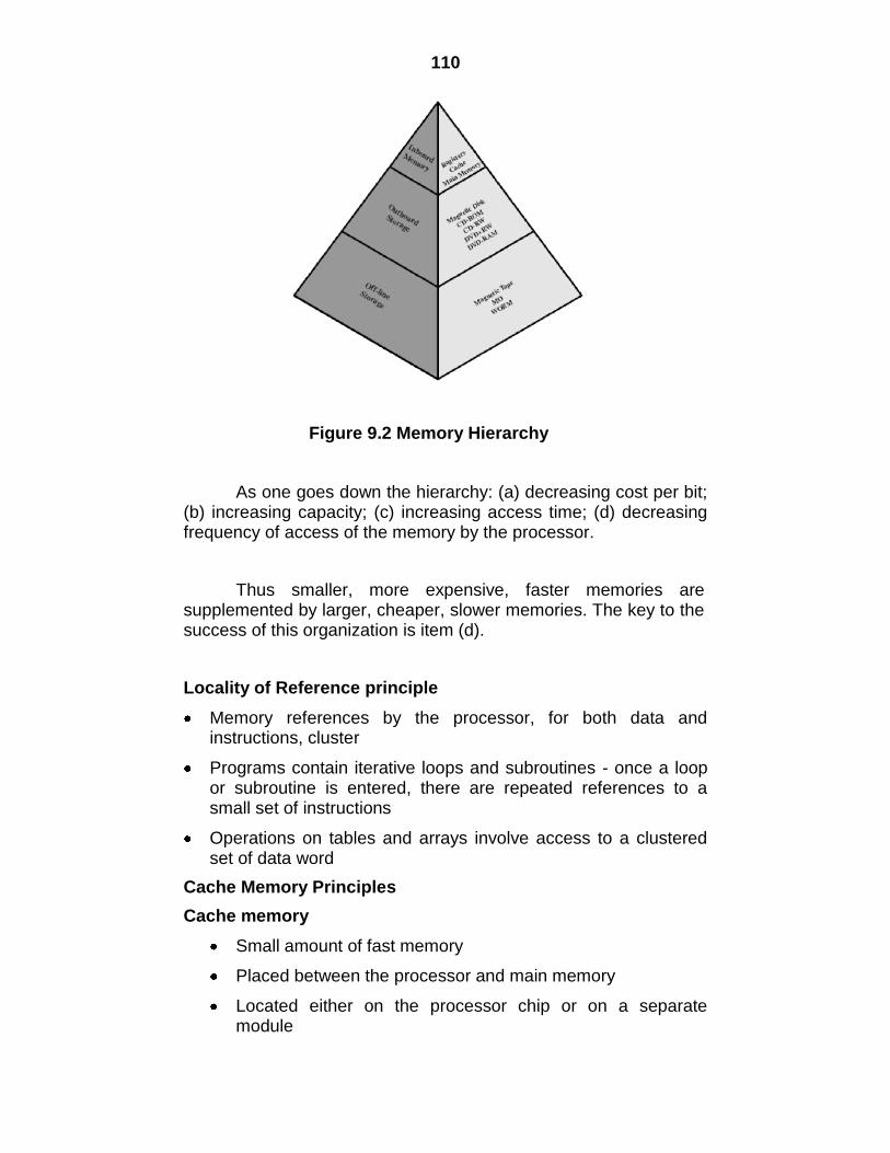
110
Figure 9.2 Memory Hierarchy
As one goes down the hierarchy: (a) decreasing cost per bit; (b) increasing capacity; (c) increasing access time; (d) decreasing frequency of access of the memory by the processor.
Thus smaller, more expensive, faster memories are supplemented by larger, cheaper, slower memories. The key to the success of this organization is item (d).
Locality of Reference principle
Memory references by the processor, for both data and instructions, cluster
Programs contain iterative loops and subroutines - once a loop or subroutine is entered, there are repeated references to a small set of instructions
Operations on tables and arrays involve access to a clustered set of data word
Cache Memory Principles
Cache memory
Small amount of fast memory
Placed between the processor and main memory
Located either on the processor chip or on a separate module
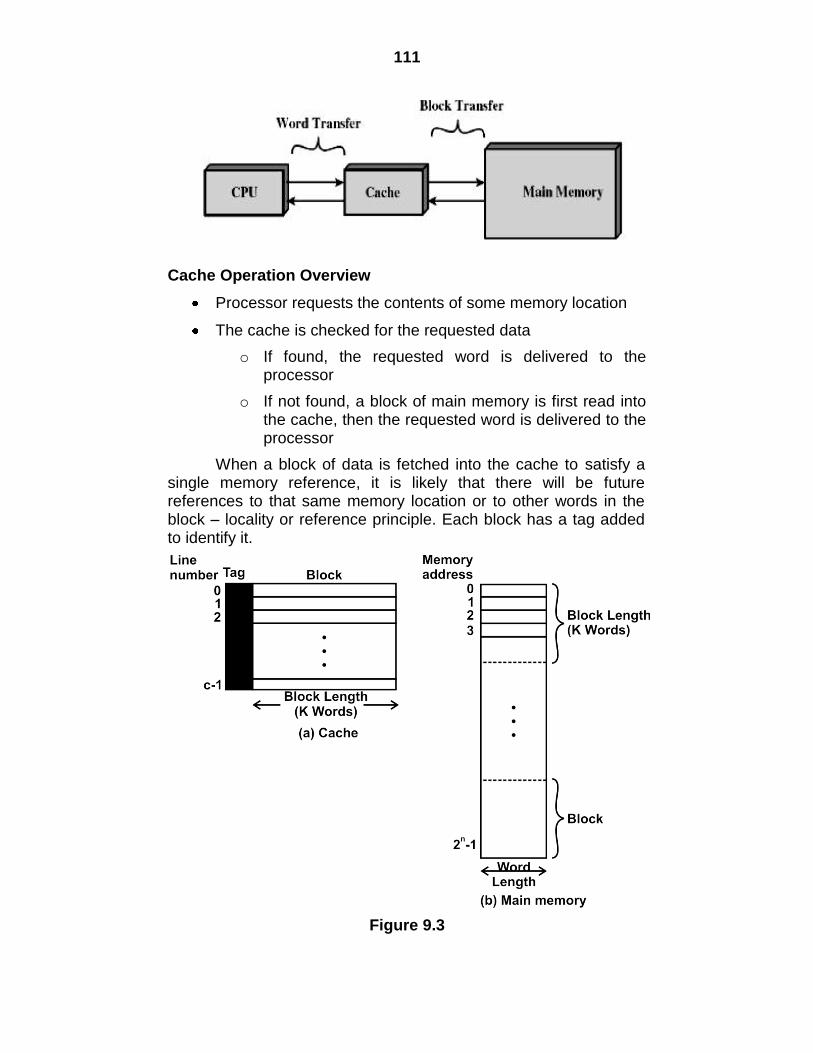
111
Cache Operation Overview
Processor requests the contents of some memory location
The cache is checked for the requested data
o If found, the requested word is delivered to the processor
o If not found, a block of main memory is first read into the cache, then the requested word is delivered to the processor
When a block of data is fetched into the cache to satisfy a single memory reference, it is likely that there will be future references to that same memory location or to other words in the block – locality or reference principle. Each block has a tag added to identify it.
Figure 9.3
112
An example of a typical cache organization is shown below :
Figure 9.4
Elements of Cache Design
Cache Size
Small enough so overall cost/bit is close to that of main memory.
Large enough so overall average access time is close to that of the cache alone.
o Access time = main memory access time plus cache access time.
Large caches tend to be slightly slower than small caches.
Cache Mapping
Mapping Function
An algorithm is needed to map main memory blocks into cache lines. A method is needed to determine which main memory block occupies a cache line. Three techniques used: direct, associative, and set associative. Assume the following:
Cache of 64 Kbytes
Transfers between main memory and cache are in blocks of 4 bytes each – cache organized as 16K = 2^14 lines of 4 bytes each
Main memory of 16 Mbytes, directly addressable by a 24-bit address (where 2^24 = 16M) – main memory consists of 4M blocks of 4 bytes each
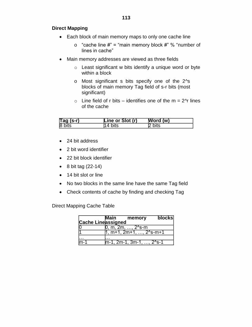
113
Direct Mapping
Each block of main memory maps to only one cache line
o “cache line #” = “main memory block #” % “number of lines in cache”
Main memory addresses are viewed as three fields
o Least significant w bits identify a unique word or byte within a block
o Most significant s bits specify one of the 2^s blocks of main memory Tag field of s-r bits (most significant)
o Line field of r bits – identifies one of the m = 2^r lines of the cache
Tag (s-r) Line or Slot (r) Word (w) 8 bits 14 bits 2 bits
24 bit address
2 bit word identifier
22 bit block identifier
8 bit tag (22-14)
14 bit slot or line
No two blocks in the same line have the same Tag field
Check contents of cache by finding and checking Tag
Direct Mapping Cache Table
Cache Line Main memory blocks assigned
0 0, m, 2m, …, 2^s-m 1 1, m+1, 2m+1, …, 2^s-m+1 … … m-1 m-1, 2m-1, 3m-1, …, 2^s-1
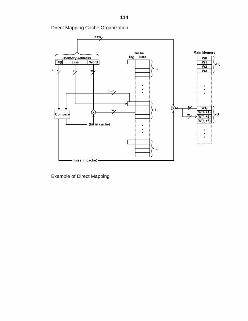
114
Direct Mapping Cache Organization
Example of Direct Mapping
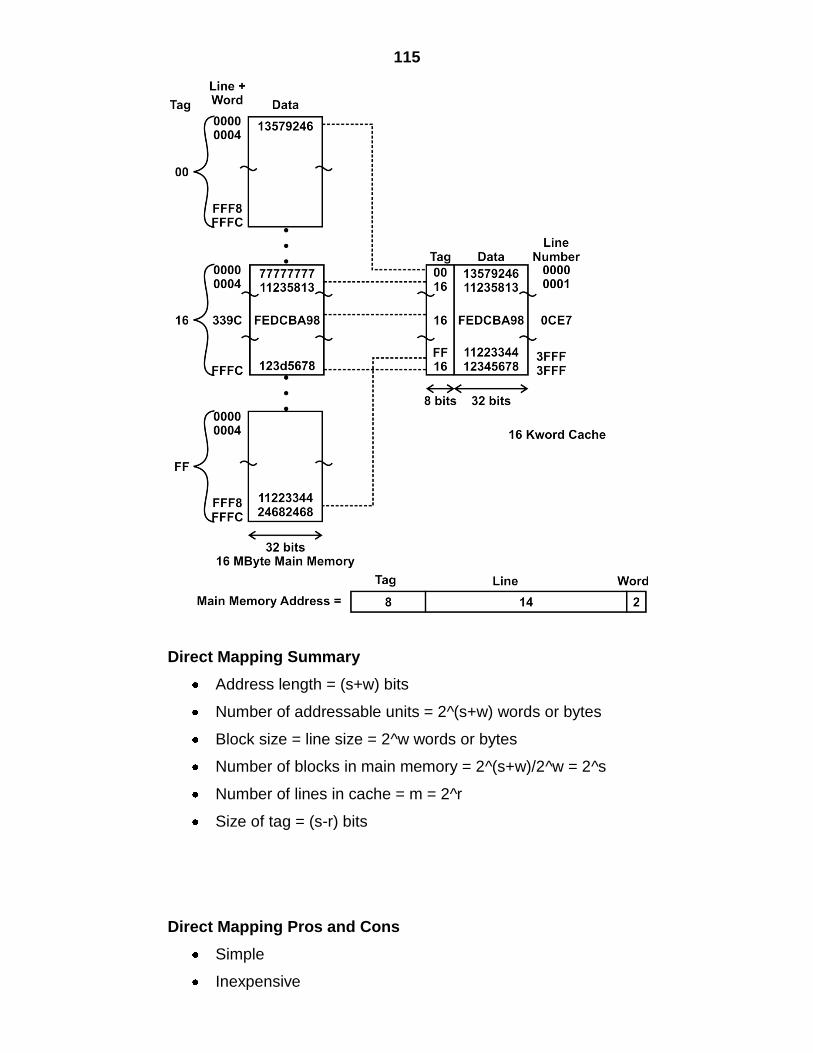
115
Direct Mapping Summary
Address length = (s+w) bits
Number of addressable units = 2^(s+w) words or bytes
Block size = line size = 2^w words or bytes
Number of blocks in main memory = 2^(s+w)/2^w = 2^s
Number of lines in cache = m = 2^r
Size of tag = (s-r) bits
Direct Mapping Pros and Cons
Simple
Inexpensive
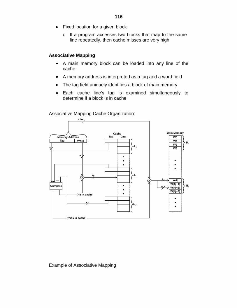
116
Fixed location for a given block
o If a program accesses two blocks that map to the same line repeatedly, then cache misses are very high
Associative Mapping
A main memory block can be loaded into any line of the cache
A memory address is interpreted as a tag and a word field
The tag field uniquely identifies a block of main memory
Each cache line‟s tag is examined simultaneously to determine if a block is in cache
Associative Mapping Cache Organization:
Example of Associative Mapping
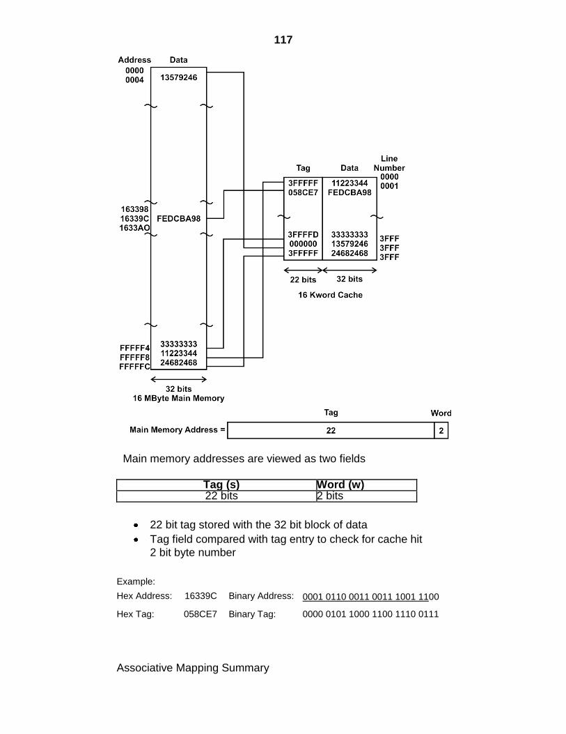
117
Main memory addresses are viewed as two fields
Tag (s) Word (w) 22 bits 2 bits
22 bit tag stored with the 32 bit block of data Tag field compared with tag entry to check for cache hit
2 bit byte number
Example:
0001 0110 0011 0011 1001 1100
Hex Address: 16339C Binary Address:
Hex Tag: 058CE7 Binary Tag: 0000 0101 1000 1100 1110 0111
Associative Mapping Summary

118
Address length = (s+w) bits
Number of addressable units = 2^(s+w) words or bytes
Block Size = line size = 2^w words or bytes
Number of blocks in main memory = 2^(s+w)/2^w = 2^s
Number of lines in cache = undetermined
Size of tag = s bits
Associative Mapping Pros and Cons
Flexibility as to which block to replace when a new block is read into cache o Replacement algorithms designed to maximize cache hit ratio
Complex circuitry required to examine the tags of all cache lines in parallel
Set Associative Mapping
Compromise between direct and associative mapping
Cache divided into v sets
Each set contains k lines
A given block maps into any line in a given set
Ex: block B can be mapped into any line in set i
Ex: Assume that k = 2 – meaning there are 2 lines per set
2-way associative mapping – k-way mapping
A given block can map into either of the 2 lines in exactly 1 set
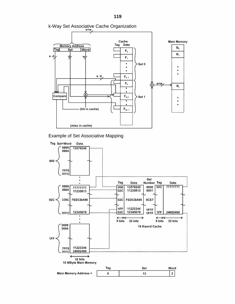
119
k-Way Set Associative Cache Organization
Example of Set Associative Mapping
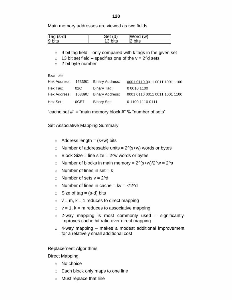
120
Main memory addresses are viewed as two fields
Tag (s-d) Set (d) Word (w) 9 bits 13 bits 2 bits
o 9 bit tag field – only compared with k tags in the given set o 13 bit set field – specifies one of the v = 2^d sets o 2 bit byte number
Example:
0001 0110 0011 0011 1001 1100
Hex Address: 16339C Binary Address:
Hex Tag: 02C Binary Tag: 0 0010 1100
Hex Address: 16339C Binary Address: 0001 0110 0011 0011 1001 1100
Hex Set: 0CE7 Binary Set: 0 1100 1110 0111
“cache set #” = “main memory block #” % “number of sets”
Set Associative Mapping Summary
o Address length = (s+w) bits
o Number of addressable units = 2^(s+w) words or bytes
o Block Size = line size = 2^w words or bytes
o Number of blocks in main memory = 2^(s+w)/2^w = 2^s
o Number of lines in set = k
o Number of sets v = 2^d
o Number of lines in cache = kv = k*2^d
o Size of tag = (s-d) bits
o v = m, k = 1 reduces to direct mapping
o v = 1, k = m reduces to associative mapping
o 2-way mapping is most commonly used – significantly improves cache hit ratio over direct mapping
o 4-way mapping – makes a modest additional improvement for a relatively small additional cost
Replacement Algorithms
Direct Mapping
o No choice
o Each block only maps to one line
o Must replace that line
121
Associative and Set Associative
Must be implemented in hardware for speed
Most effective – Least Recently Used (LRU)
Replace the block in the set that has been in cache the longest with no references to it
o 2-way set associative – each line includes a USE bit
First-in-first-out (FIFO)
o Replace the block in the set that has been in the cache the longest
o Uses a round-robin or circular buffer technique
Least Frequently Used (LFU)
o Replace the block in the set that has experienced the fewest references
o Associate a counter with each line
Pick a line at random – not based usage
o Only slightly inferior in performance to algorithms based on usage
Write Policy
o What if cache has been altered and main memory doesn‟t match must write to memory before replacing the word in cache
o What if multiple processors are present and each one has its own cache
o What if an I/O device addresses main memory directly
Write Through
o All writes go to both cache and main memory
o Each processor can monitor main memory activity to keep local cache current
o Generates a lot of memory traffic
Write Back
o Minimizes memory writes
o Updates are made only in cache
o UPDATE bit associated with the line is set
o When the block is replaced it is written back to main memory only if the UPDATE bit is set
o This may cause other caches to be out of sync
o I/O must access main memory through the cache
o 15% of memory references are writes
122
Exercise
Q1. Explain the usage of memory.
Q2. Explain RAM and ROM.
Q3. Explain different types of ROM.
Q4. Explain the concept of cache memory.
Q5. Explain different characteristics of Memory Systems.
Q6. Explain Cache mapping.
References
Computer System Architecture – M. Morris Meno, PHI, 1998
Computer Architecture and Organization - John P Hayes, McGraw Hill, 1998
Digital Computer Fundamentals – Malvino
Digital Computer Fundamentals – Thomas C Bartee, TMG
Computer Organization and Architecture – William Stallings
Microprocessor Architecture and Programming and Applications with the 8085 – R.S. Gaonkar, PRI
123
10
EXTERNAL MEMORY
Topics Covered:
10.1 Introduction
10.2 Magnetic Disk
10.3 Data Organization and Formatting
10.4 RAID
10.1 INTRODUCTION
Magnetic disks remain the most important component of external memory.
Both removable and fixed, hard disks are used in systems ranging from personal computers to mainframes and supercomputers.
To achieve greater performance and higher availability, a popular scheme on servers and larger systems is the RAID disk technology.
RAID refers to a family of techniques for using multiple disks as a parallel array of data storage devices, with redundancy built in to compensate for disk failure.
Optical storage technology has become increasingly important in all types of computer systems.
While CD-ROM has been widely used for many years, more recent technologies, such as writable CD and DVD, are becoming increasingly important.
10.2 MAGNETIC DISK
Circular platter constructed of nonmagnetic material, called the substrate, coated with a magnetize able material
Substrate was traditionally aluminum or aluminum alloy Substrate now glass
o Improved surface uniformity – increased reliability o Reduction in surface defects – reduce read/write
errors o Support lower fly heights o Greater ability to withstand shock and damage
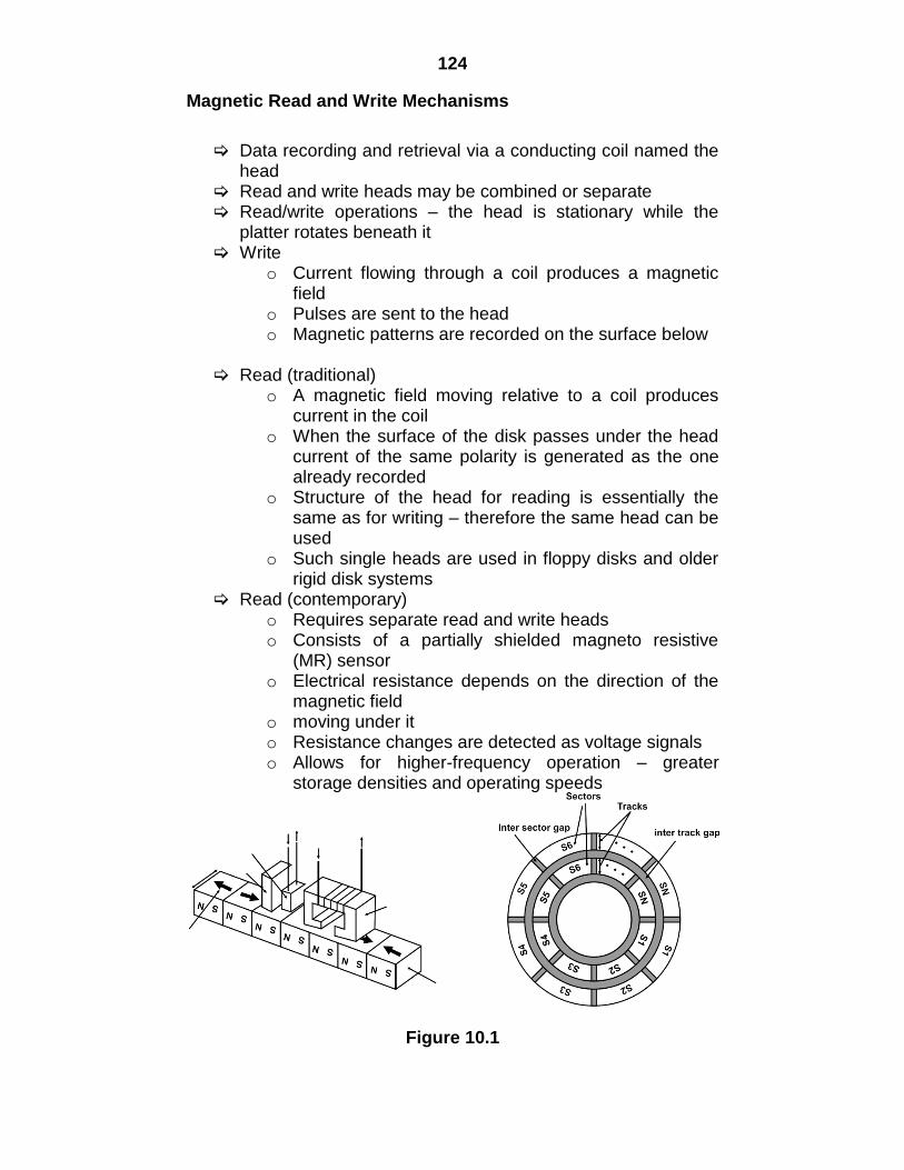
124
Magnetic Read and Write Mechanisms
Data recording and retrieval via a conducting coil named the head
Read and write heads may be combined or separate Read/write operations – the head is stationary while the
platter rotates beneath it Write
o Current flowing through a coil produces a magnetic field
o Pulses are sent to the head o Magnetic patterns are recorded on the surface below
Read (traditional) o A magnetic field moving relative to a coil produces
current in the coil o When the surface of the disk passes under the head
current of the same polarity is generated as the one already recorded
o Structure of the head for reading is essentially the same as for writing – therefore the same head can be used
o Such single heads are used in floppy disks and older rigid disk systems
Read (contemporary) o Requires separate read and write heads o Consists of a partially shielded magneto resistive
(MR) sensor o Electrical resistance depends on the direction of the
magnetic field o moving under it o Resistance changes are detected as voltage signals o Allows for higher-frequency operation – greater
storage densities and operating speeds
Figure 10.1
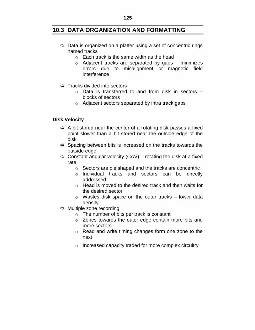
125
10.3 DATA ORGANIZATION AND FORMATTING
Data is organized on a platter using a set of concentric rings named tracks
o Each track is the same width as the head o Adjacent tracks are separated by gaps – minimizes
errors due to misalignment or magnetic field interference
Tracks divided into sectors
o Data is transferred to and from disk in sectors – blocks of sectors
o Adjacent sectors separated by intra track gaps
Disk Velocity
A bit stored near the center of a rotating disk passes a fixed point slower than a bit stored near the outside edge of the disk
Spacing between bits is increased on the tracks towards the outside edge
Constant angular velocity (CAV) – rotating the disk at a fixed rate
o Sectors are pie shaped and the tracks are concentric o Individual tracks and sectors can be directly
addressed o Head is moved to the desired track and then waits for
the desired sector o Wastes disk space on the outer tracks – lower data
density Multiple zone recording
o The number of bits per track is constant o Zones towards the outer edge contain more bits and
more sectors o Read and write timing changes form one zone to the
next
o Increased capacity traded for more complex circuitry
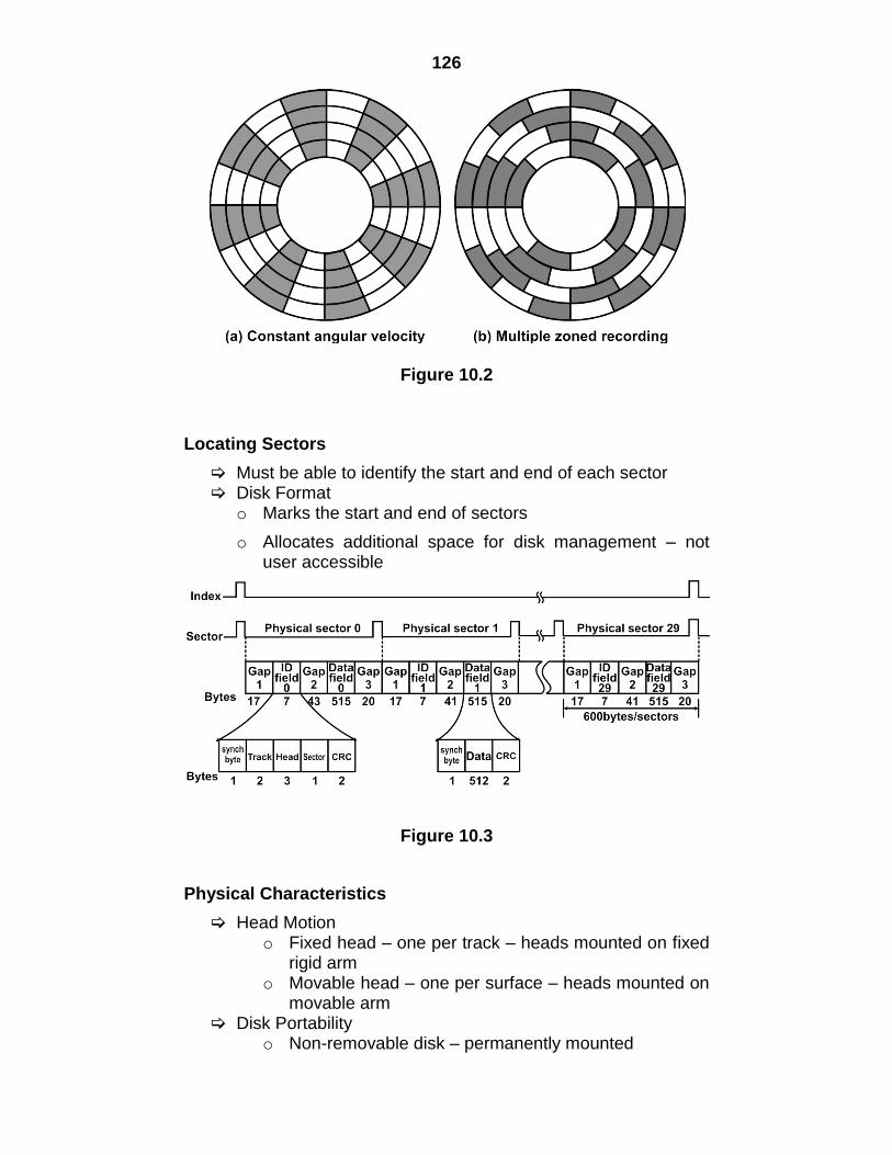
126
Figure 10.2
Locating Sectors
Must be able to identify the start and end of each sector Disk Format
o Marks the start and end of sectors
o Allocates additional space for disk management – not user accessible
Figure 10.3
Physical Characteristics
Head Motion o Fixed head – one per track – heads mounted on fixed
rigid arm o Movable head – one per surface – heads mounted on
movable arm Disk Portability
o Non-removable disk – permanently mounted
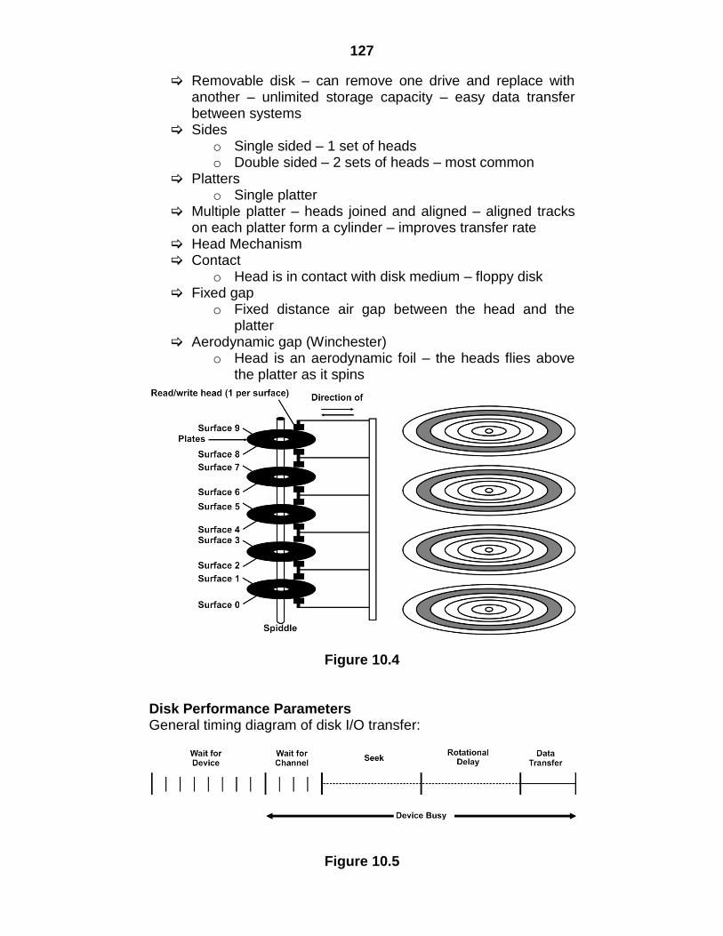
127
Removable disk – can remove one drive and replace with another – unlimited storage capacity – easy data transfer between systems
Sides o Single sided – 1 set of heads o Double sided – 2 sets of heads – most common
Platters o Single platter
Multiple platter – heads joined and aligned – aligned tracks on each platter form a cylinder – improves transfer rate
Head Mechanism Contact
o Head is in contact with disk medium – floppy disk Fixed gap
o Fixed distance air gap between the head and the platter
Aerodynamic gap (Winchester) o Head is an aerodynamic foil – the heads flies above
the platter as it spins
Figure 10.4 Disk Performance Parameters General timing diagram of disk I/O transfer:
Figure 10.5
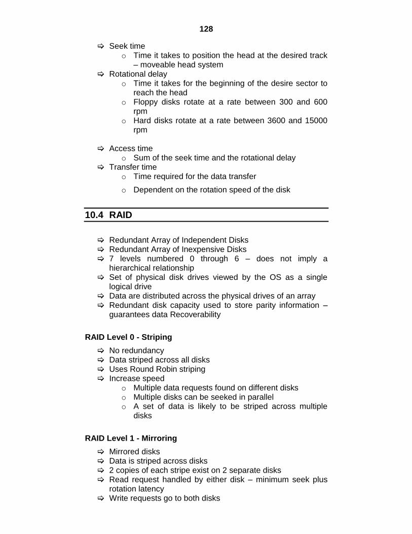
128
Seek time o Time it takes to position the head at the desired track
– moveable head system Rotational delay
o Time it takes for the beginning of the desire sector to reach the head
o Floppy disks rotate at a rate between 300 and 600 rpm
o Hard disks rotate at a rate between 3600 and 15000 rpm
Access time
o Sum of the seek time and the rotational delay Transfer time
o Time required for the data transfer
o Dependent on the rotation speed of the disk
10.4 RAID
Redundant Array of Independent Disks Redundant Array of Inexpensive Disks 7 levels numbered 0 through 6 – does not imply a
hierarchical relationship Set of physical disk drives viewed by the OS as a single
logical drive Data are distributed across the physical drives of an array Redundant disk capacity used to store parity information –
guarantees data Recoverability
RAID Level 0 - Striping
No redundancy Data striped across all disks Uses Round Robin striping Increase speed
o Multiple data requests found on different disks o Multiple disks can be seeked in parallel o A set of data is likely to be striped across multiple
disks
RAID Level 1 - Mirroring
Mirrored disks Data is striped across disks 2 copies of each stripe exist on 2 separate disks Read request handled by either disk – minimum seek plus
rotation latency Write requests go to both disks
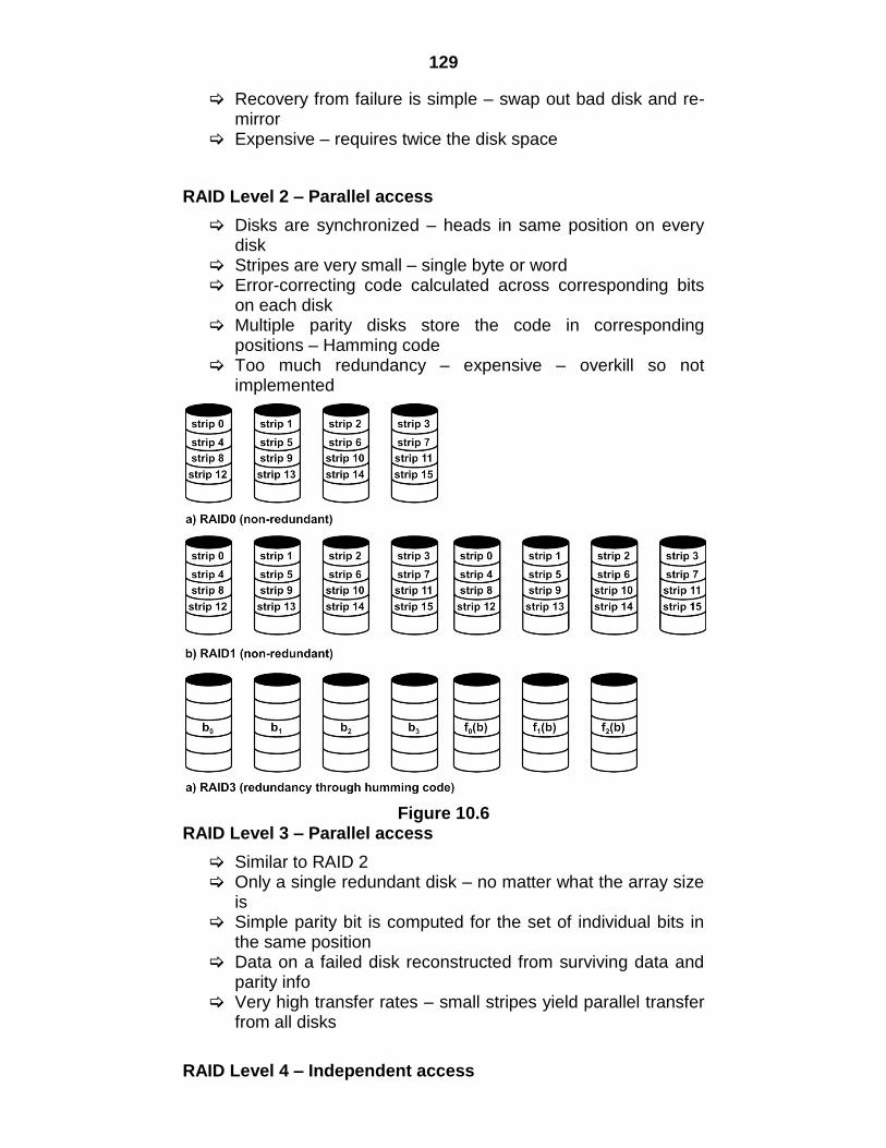
129
Recovery from failure is simple – swap out bad disk and re-mirror
Expensive – requires twice the disk space
RAID Level 2 – Parallel access
Disks are synchronized – heads in same position on every disk
Stripes are very small – single byte or word Error-correcting code calculated across corresponding bits
on each disk Multiple parity disks store the code in corresponding
positions – Hamming code Too much redundancy – expensive – overkill so not
implemented
Figure 10.6 RAID Level 3 – Parallel access
Similar to RAID 2 Only a single redundant disk – no matter what the array size
is Simple parity bit is computed for the set of individual bits in
the same position Data on a failed disk reconstructed from surviving data and
parity info Very high transfer rates – small stripes yield parallel transfer
from all disks
RAID Level 4 – Independent access
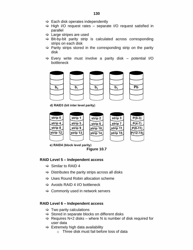
130
Each disk operates independently High I/O request rates – separate I/O request satisfied in
parallel Large stripes are used Bit-by-bit parity strip is calculated across corresponding
strips on each disk Parity strips stored in the corresponding strip on the parity
disk
Every write must involve a parity disk – potential I/O bottleneck
Figure 10.7
RAID Level 5 – Independent access
Similar to RAID 4
Distributes the parity strips across all disks
Uses Round Robin allocation scheme
Avoids RAID 4 I/O bottleneck
Commonly used in network servers
RAID Level 6 – Independent access
Two parity calculations Stored in separate blocks on different disks Requires N+2 disks – where N is number of disk required for
user data Extremely high data availability
o Three disk must fail before loss of data
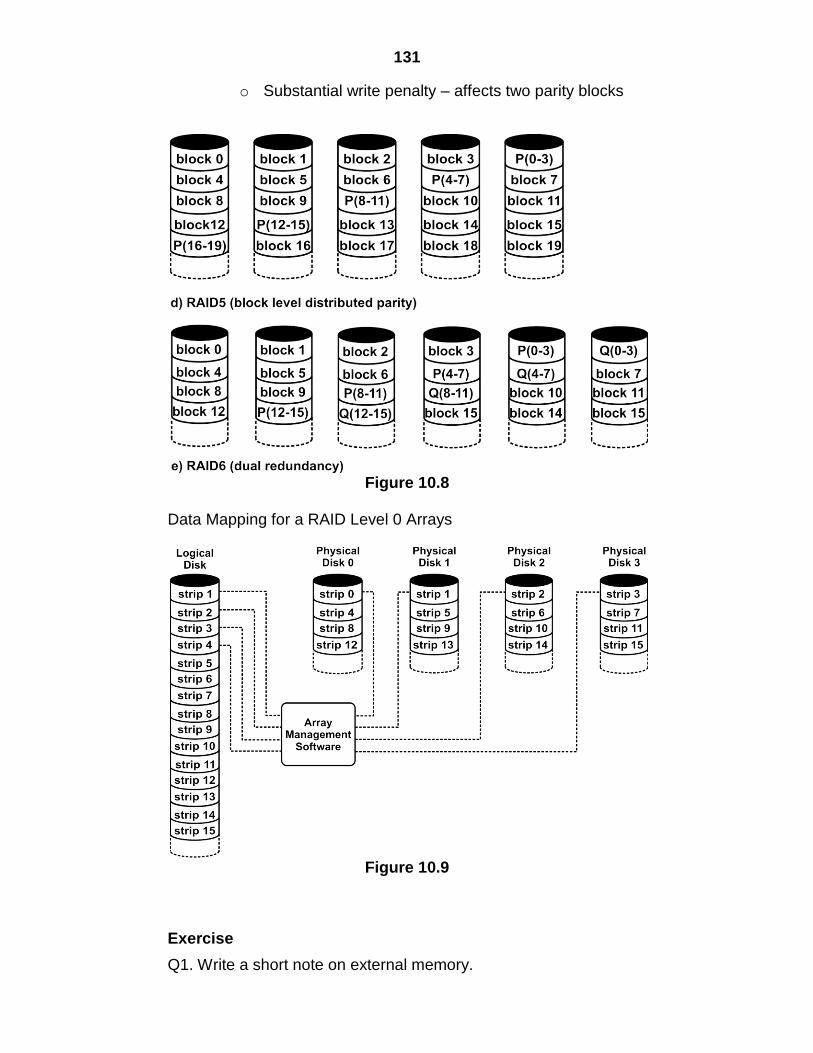
131
o Substantial write penalty – affects two parity blocks
Figure 10.8
Data Mapping for a RAID Level 0 Arrays
Figure 10.9
Exercise
Q1. Write a short note on external memory.
132
Q2. Explain RAID memory with different levels.
References
Computer System Architecture – M. Morris Meno, PHI, 1998
Computer Architecture and Organization - John P Hayes, McGraw Hill, 1998
Digital Computer Fundamentals – Malvino
Digital Computer Fundamentals – Thomas C Bartee, TMG
Computer Organization and Architecture – William Stallings
Microprocessor Architecture and Programming and Applications with the 8085 – R.S. Gaonkar, PRI
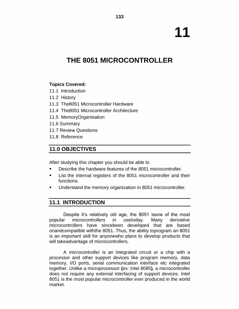
133
11
THE 8051 MICROCONTROLLER
Topics Covered:
11.1 Introduction
11.2 History
11.3 The8051 Microcontroller Hardware
11.4 The8051 Microcontroller Architecture
11.5 MemoryOrganisation
11.6 Summary
11.7 Review Questions
11.8 Reference
11.0 OBJECTIVES
After studying this chapter you should be able to
Describe the hardware features of the 8051 microcontroller.
List the internal registers of the 8051 microcontroller and their functions.
Understand the memory organization in 8051 microcontroller.
11.1 INTRODUCTION
Despite it‟s relatively old age, the 8051 isone of the most
popular microcontrollers in usetoday. Many derivative microcontrollers have sincebeen developed that are based onandcompatible withthe 8051. Thus, the ability toprogram an 8051 is an important skill for anyonewho plans to develop products that will takeadvantage of microcontrollers.
A microcontroller is an integrated circuit or a chip with a
processor and other support devices like program memory, data memory, I/O ports, serial communication interface etc integrated together. Unlike a microprocessor (ex: Intel 8085), a microcontroller does not require any external interfacing of support devices. Intel 8051 is the most popular microcontroller ever produced in the world market.
134
11.2 HISTORY
Intel, first produced a microcontroller in 1976 under the
name MCS-48, which is an 8 bit microcontroller. Later in 1980 they released a further improved version (which is also 8 bit), under the name MCS-51. The most popular microcontroller 8051 belongs to the MCS-51 family of microcontrollers by Intel. Following the success of 8051, many other semiconductor manufacturers released microcontrollers under their own brand name but using the MCS-51 core. Global companies and giants in semiconductor industry like Microchip, Zilog, Atmel, Philips, Siemens released products under their brand name. The specialty was that all these devices could be programmed using the same MCS-51 instruction sets. They basically differed in support device configurations like improved memory, presence of an ADC or DAC etc.
11.2.1 8051 Family
Intel fabricated the original 8051 which is known as MCS-51. The other two members of the 8051 family are:
I] 8052 – This microcontroller has 256 bytes of RAM and 3 timers. In addition to the standard features of 8051, this microcontroller has an added 128 bytes of RAM and timer. It has 8K bytes of on chip program ROM. The programs written for projects using 8051 microcontroller can be used to run on the projects using 8052 microcontroller as 8051 is a subset of 8052.
II] 8031 – This microcontroller has all the features of 8051 except for it to be ROM-less. An external ROM that can be as large as 64 K bytes should be programmed and added to this chip for execution. The disadvantage of adding external ROM is that 2 ports (out of the 4 ports) are used. Hence, only 2 ports are left for I/O operations which can also be added externally if required for execution.
Comparison of 8051 family members:
Features 8051 8052 8031
RAM(bytes) 128 256 128
ROM 4K 8K 0K
Timers 2 3 2
Serial port 1 1 1
I/O pins 32 32 32
Interrupt sources 6 8 6
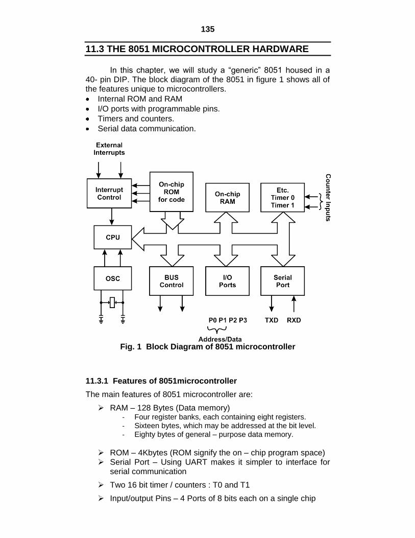
135
11.3 THE 8051 MICROCONTROLLER HARDWARE
In this chapter, we will study a “generic” 8051 housed in a 40- pin DIP. The block diagram of the 8051 in figure 1 shows all of the features unique to microcontrollers.
Internal ROM and RAM
I/O ports with programmable pins.
Timers and counters.
Serial data communication.
Fig. 1 Block Diagram of 8051 microcontroller
11.3.1 Features of 8051microcontroller
The main features of 8051 microcontroller are:
RAM – 128 Bytes (Data memory) - Four register banks, each containing eight registers. - Sixteen bytes, which may be addressed at the bit level. - Eighty bytes of general – purpose data memory.
ROM – 4Kbytes (ROM signify the on – chip program space) Serial Port – Using UART makes it simpler to interface for
serial communication
Two 16 bit timer / counters : T0 and T1
Input/output Pins – 4 Ports of 8 bits each on a single chip
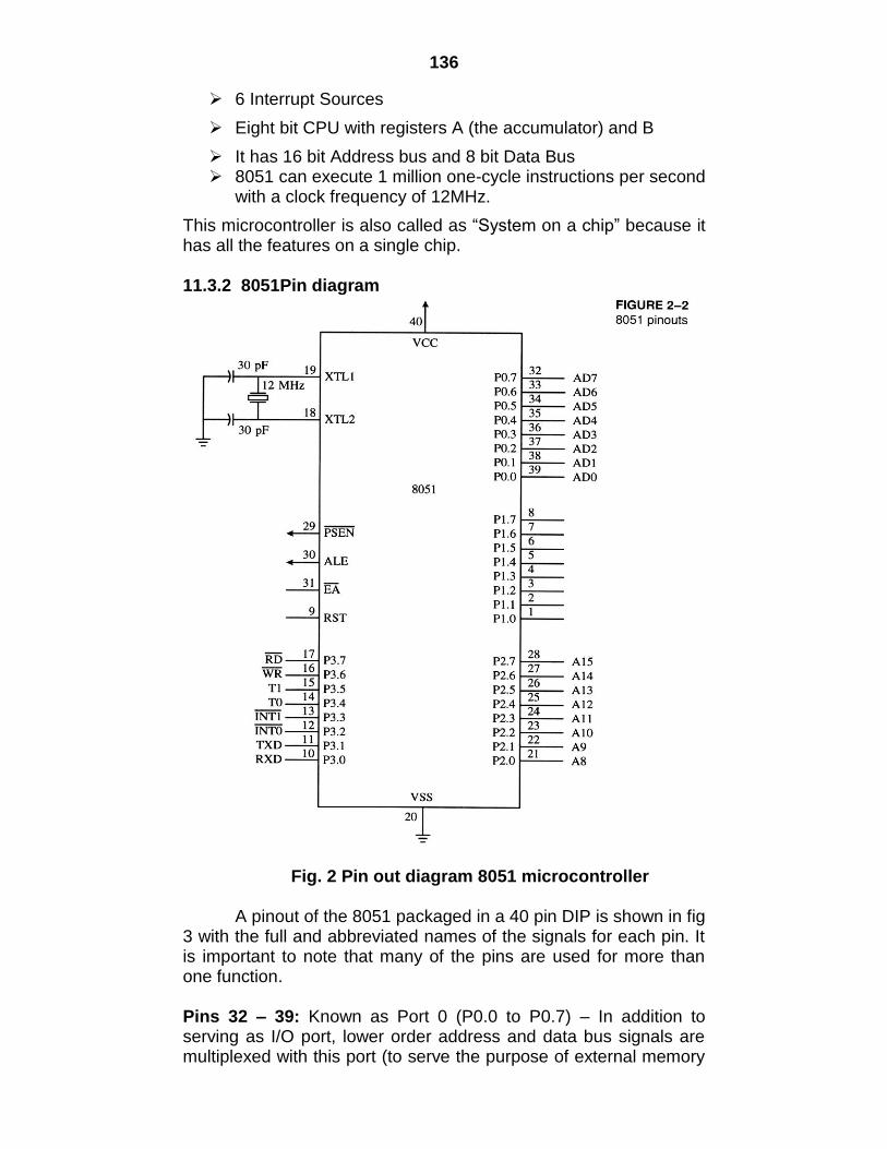
136
6 Interrupt Sources
Eight bit CPU with registers A (the accumulator) and B
It has 16 bit Address bus and 8 bit Data Bus 8051 can execute 1 million one-cycle instructions per second
with a clock frequency of 12MHz.
This microcontroller is also called as “System on a chip” because it has all the features on a single chip. 11.3.2 8051Pin diagram
Fig. 2 Pin out diagram 8051 microcontroller
A pinout of the 8051 packaged in a 40 pin DIP is shown in fig 3 with the full and abbreviated names of the signals for each pin. It is important to note that many of the pins are used for more than one function.
Pins 32 – 39: Known as Port 0 (P0.0 to P0.7) – In addition to serving as I/O port, lower order address and data bus signals are multiplexed with this port (to serve the purpose of external memory
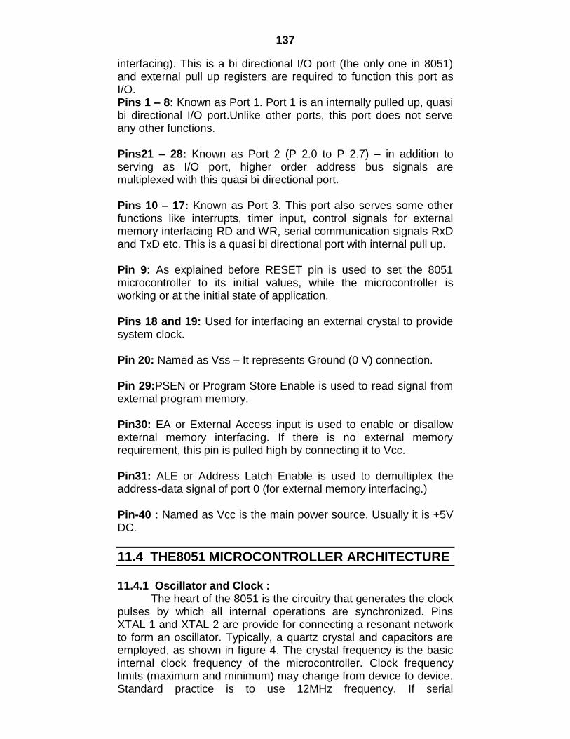
137
interfacing). This is a bi directional I/O port (the only one in 8051) and external pull up registers are required to function this port as I/O. Pins 1 – 8: Known as Port 1. Port 1 is an internally pulled up, quasi bi directional I/O port.Unlike other ports, this port does not serve any other functions. Pins21 – 28: Known as Port 2 (P 2.0 to P 2.7) – in addition to serving as I/O port, higher order address bus signals are multiplexed with this quasi bi directional port. Pins 10 – 17: Known as Port 3. This port also serves some other functions like interrupts, timer input, control signals for external memory interfacing RD and WR, serial communication signals RxD and TxD etc. This is a quasi bi directional port with internal pull up. Pin 9: As explained before RESET pin is used to set the 8051 microcontroller to its initial values, while the microcontroller is working or at the initial state of application. Pins 18 and 19: Used for interfacing an external crystal to provide system clock. Pin 20: Named as Vss – It represents Ground (0 V) connection. Pin 29:PSEN or Program Store Enable is used to read signal from external program memory. Pin30: EA or External Access input is used to enable or disallow external memory interfacing. If there is no external memory requirement, this pin is pulled high by connecting it to Vcc. Pin31: ALE or Address Latch Enable is used to demultiplex the address-data signal of port 0 (for external memory interfacing.) Pin-40 : Named as Vcc is the main power source. Usually it is +5V DC.
11.4 THE8051 MICROCONTROLLER ARCHITECTURE
11.4.1 Oscillator and Clock : The heart of the 8051 is the circuitry that generates the clock pulses by which all internal operations are synchronized. Pins XTAL 1 and XTAL 2 are provide for connecting a resonant network to form an oscillator. Typically, a quartz crystal and capacitors are employed, as shown in figure 4. The crystal frequency is the basic internal clock frequency of the microcontroller. Clock frequency limits (maximum and minimum) may change from device to device. Standard practice is to use 12MHz frequency. If serial
138
communications are involved then its best to use 11.0592 MHz frequency.
Fig. 3 To calculate the time any particular instruction will take to be executed, and the number of cycles, C. The time to execute that instruction is then found by multiplying C by 12 and dividing the product by the crystal frequency :
12inst
C dT
Crystal frequency
For example, if the crystal frequency is 16 megahertz, then the time to execute an ADD A, R1 one-cycle instruction is .75 micro seconds. A 12 megahertz crystal yields the convenient time of 1 microsecond per cycle. An 11.0592 megahertz crystal, although seemingly an odd value, yields a cycle frequency of 921.6 kilohertz. 11.4.2 Program Counter and Data Pointer The 8051 contains two 16 bit registers : The program counter (PC) and the data pointer (DPTR). Each is used to hold the address of a byte in memory. The Program Counter (PC) is a 2-byte address which tells the 8051 where the next instruction to execute is found in memory. When the 8051 is initialized PC always starts at 0000h and is incremented each time an instruction is executed. It is important to note that PC is not always incremented by one. Since some instructions require 2 or 3 bytes the PC will be incremented by 2 or 3 in these cases.
The Data PointerDPTR, as the name suggests, is used to point to data. The DPTR register is made up of two 8 bit registers, named DPH and DPL, which are used to furnish memory addresses for internal and external code access and external data access. The DPTR is under the control of program instructions and
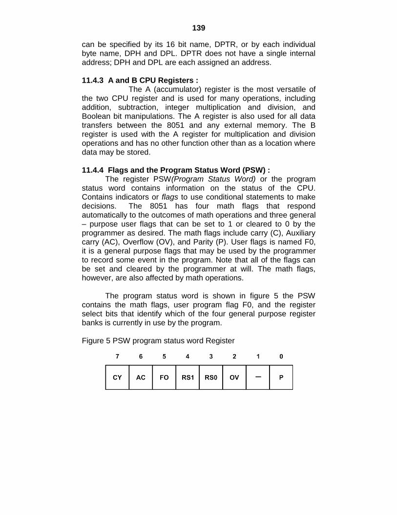
139
can be specified by its 16 bit name, DPTR, or by each individual byte name, DPH and DPL. DPTR does not have a single internal address; DPH and DPL are each assigned an address. 11.4.3 A and B CPU Registers : The A (accumulator) register is the most versatile of the two CPU register and is used for many operations, including addition, subtraction, integer multiplication and division, and Boolean bit manipulations. The A register is also used for all data transfers between the 8051 and any external memory. The B register is used with the A register for multiplication and division operations and has no other function other than as a location where data may be stored. 11.4.4 Flags and the Program Status Word (PSW) : The register PSW(Program Status Word) or the program status word contains information on the status of the CPU. Contains indicators or flags to use conditional statements to make decisions. The 8051 has four math flags that respond automatically to the outcomes of math operations and three general – purpose user flags that can be set to 1 or cleared to 0 by the programmer as desired. The math flags include carry (C), Auxiliary carry (AC), Overflow (OV), and Parity (P). User flags is named F0, it is a general purpose flags that may be used by the programmer to record some event in the program. Note that all of the flags can be set and cleared by the programmer at will. The math flags, however, are also affected by math operations. The program status word is shown in figure 5 the PSW contains the math flags, user program flag F0, and the register select bits that identify which of the four general purpose register banks is currently in use by the program. Figure 5 PSW program status word Register
140
The Program Status Word (PSW) is a Special Function Register
Bit Symbol Function
7 CY Carry Flag : Used in arithmetic, jump, rotate, and Boolean instructions.
6 AC Auxiliary Carry Flag : Used for BCD arithmetic
5 FO User flag 0
4 RS1 Register Bank Select bit 1
3 RS0 Register Bank Select bit 0
RS1 RS0
0 0 Select Register Bank 0
0 1 Select Register Bank 1
1 0 Select Register Bank 2
1 1 Select Register Bank 3
2 OV Overflow flag: Used in arithmetic instructions.
1 - Reserved for future use
0
P Parity Flag: Shows parity of register A : 1 = odd parity.
Bit Addressable as PSW 0 to PSW 7
11.4.5 Stack Pointer The stack pointer indicates where the next value to be taken from the stack will be read from in internal RAM. If you push a value on to the stack, the value will be written to the address SP + 1. If SP holds the value 07h, a PUSH instruction will push the value onto the stack address 08h. The stack pointer is modified by instructions such as PUSH, POP, LCALL, RET, RETI and whenever interrupts are provoked by the microcontroller.
11.5 MEMORY ORGANISATION
The 8051 has two types of memory and these are Program Memory and Data Memory. Program Memory (ROM) is used to permanently save the program being executed, while Data Memory (RAM) is used for temporarily storing data and intermediate results created and used during the operation of the microcontroller. All 8051 microcontrollers have a 16-bit addressing bus and are capable of addressing 64 kb memory.
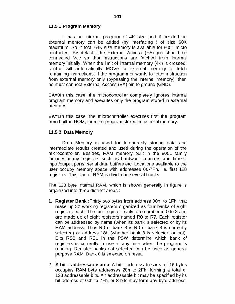
141
11.5.1 Program Memory
It has an internal program of 4K size and if needed an external memory can be added (by interfacing ) of size 60K maximum. So in total 64K size memory is available for 8051 micro controller. By default, the External Access (EA) pin should be connected Vcc so that instructions are fetched from internal memory initially. When the limit of internal memory (4K) is crossed, control will automatically MOVe to external memory to fetch remaining instructions. If the programmer wants to fetch instruction from external memory only (bypassing the internal memory), then he must connect External Access (EA) pin to ground (GND).
EA=0In this case, the microcontroller completely ignores internal program memory and executes only the program stored in external memory. EA=1In this case, the microcontroller executes first the program from built-in ROM, then the program stored in external memory. 11.5.2 Data Memory Data Memory is used for temporarily storing data and intermediate results created and used during the operation of the microcontroller. Besides, RAM memory built in the 8051 family includes many registers such as hardware counters and timers, input/output ports, serial data buffers etc. Locations available to the user occupy memory space with addresses 00-7Fh, i.e. first 128 registers. This part of RAM is divided in several blocks. The 128 byte internal RAM, which is shown generally in figure is organized into three distinct areas : 1. Register Bank :Thirty two bytes from address 00h to 1Fh, that
make up 32 working registers organized as four banks of eight registers each. The four register banks are numbered 0 to 3 and are made up of eight registers named R0 to R7. Each register can be addressed by name (when its bank is selected or by its RAM address. Thus R0 of bank 3 is R0 (if bank 3 is currently selected) or address 18h (whether bank 3 is selected or not). Bits RS0 and RS1 in the PSW determine which bank of registers is currently in use at any time when the program is running. Register banks not selected can be used as general purpose RAM. Bank 0 is selected on reset.
2. A bit – addressable area: A bit – addressable area of 16 bytes occupies RAM byte addresses 20h to 2Fh, forming a total of 128 addressable bits. An addressable bit may be specified by its bit address of 00h to 7Fh, or 8 bits may form any byte address.
142
From 20h to 2Fh. Thus, For example, bit address 4Fh is also bit 7 of byte address 29 h.
3. A general purpose RAM:A general purpose RAM area above
the bit area, from 30h to 70h, addressable as bytes.
Figure: Memory (a)
143
11.6 SUMMARY
A microcontroller is an integrated circuit or a chip with a
processor and other support devices like program memory, data memory, I/O ports, serial communication interface etc integrated together.
Unique features of microcontrollers.
Internal ROM and RAM
I/O ports with programmable pins
Timers and counters
Serial data communication
The Program Counter (PC) is a 2-byte address which tells the 8051 where the next instruction to execute is found in memory.
The crystal frequency is the basic internal clock frequency of
the microcontroller. Clock frequency limits (maximum and minimum) may change from device to device. Standard practice is to use 12MHz frequency.
The DPTR register is made up of two 8 bit registers, named DPH
and DPL, which are used to furnish memory addresses for internal and external code access and external data access.
The A (accumulator) register is the most versatile of the two
CPU register and is used for many operations, including addition, subtraction, integer multiplication and division, and Boolean bit manipulations.
The stack pointer indicates where the next value to be taken
from the stack will be read from in internal RAM. The PSW(Program Status Word) contains information
offlags.This includes carry (C), Auxiliary carry (AC), Overflow (OV), and Parity (P), user flag F0 and RS0 & RS1 to select Register bank.
RAM memory built in the 8051 family includes many
registers such as hardware counters and timers, input/output ports, serial data buffers etc. Locations available to the user occupy memory space with addresses 00-7Fh, i.e. first 128 registers.
144
11.7 REVIEW QUESTIONS
Q.1 Describe in brief the history of 8051.
Q.2 Draw and explain the block diagram of inside the microcontroller 8051.
Q.3 State the features of 8051 microcontroller.
Q.4 Describe the program counter in the 8051.
Q.5 Describe the stack pointer in the 8051.
Q.6 Explain the role of DPTR register in the 8051.
Q.8 Compare the features of 8031, 8051
Q.9 Write a note on PSW register.
Q.10 Describe the various flags used along with their functions in the 8051.
Q.11 Explain the oscillator and clock in the 8051.
Q.12 How the RAM of 8051 is organized?
11.7 REFERENCE
The 8051 Microcontroller by Kenneth J. Ayala, Publisher: Thomson Delmar Learning
The 8051 Microcontroller And Embedded Systems Using
Assembly And C, 2/E By Mazidi and Mazidi, Publisher: Pearson Education India
145
12 THE 8051 MICROCONTROLLER ...continued
12.1 Objectives
12.2 Special Function Registers
12.3Counter and timers
12.4 Serial communication
12.4 Interrupts
12.5 Summary
12.6 Review Questions
12.7 Reference
12.1 OBJECTIVES
After studying this chapter you should be able to Describe the SFR in the 8051 microcontroller Understand the working of counters in the 8051 Understand the interrupts in the 8051
12.2 SPECIAL FUNCTION REGISTERS
The 8051 operations that do not use the internal 128-byte
RAM addresses from 00h to 7Fh are done by a group of specific internal registers, each called a special Function register (SFR), which may be addressed much like internal RAM using addresses from 80h to FFh. Some SFRs (marked with an asterick * in figure) are also bit addressable, as is the case for the bit area of RAM. This feature allows the programmer to change only what needs to be altered, leaving the remaining bits in that SFR unchanged.
Not all of the addresses from 80h to FFh are used for SFRs, and attempting to use an address that is not defined or empty, results in unpredictable results. The SFR names and equivalent internal RAM addresses are given in the following list :
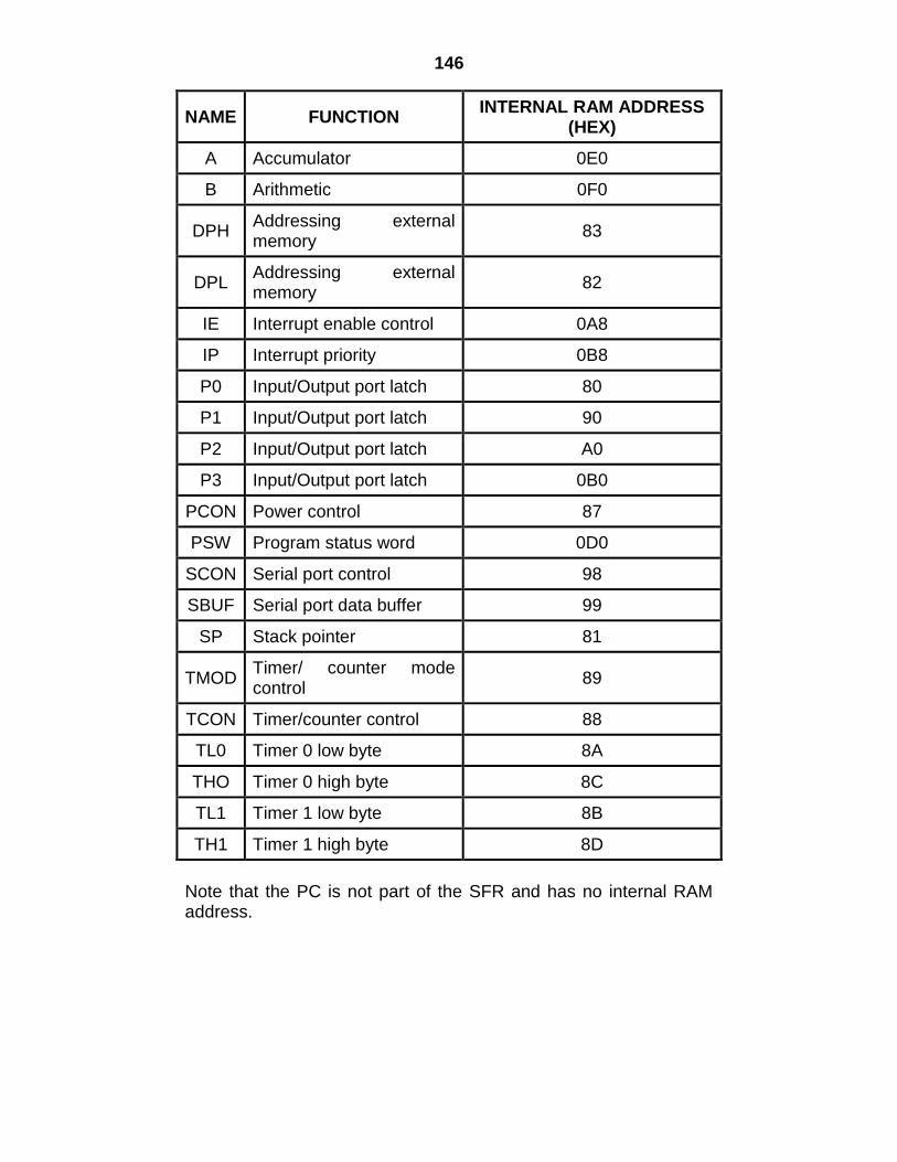
146
NAME FUNCTION INTERNAL RAM ADDRESS
(HEX)
A Accumulator 0E0
B Arithmetic 0F0
DPH Addressing external memory
83
DPL Addressing external memory
82
IE Interrupt enable control 0A8
IP Interrupt priority 0B8
P0 Input/Output port latch 80
P1 Input/Output port latch 90
P2 Input/Output port latch A0
P3 Input/Output port latch 0B0
PCON Power control 87
PSW Program status word 0D0
SCON Serial port control 98
SBUF Serial port data buffer 99
SP Stack pointer 81
TMOD Timer/ counter mode control
89
TCON Timer/counter control 88
TL0 Timer 0 low byte 8A
THO Timer 0 high byte 8C
TL1 Timer 1 low byte 8B
TH1 Timer 1 high byte 8D
Note that the PC is not part of the SFR and has no internal RAM address.
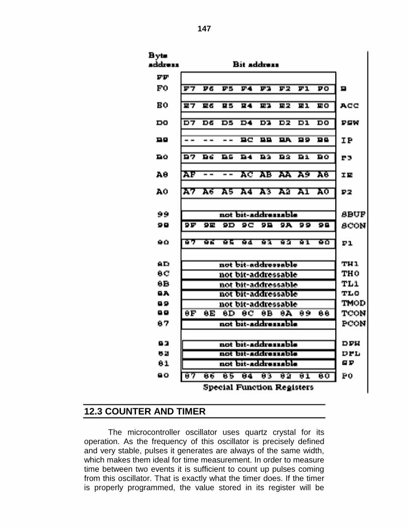
147
12.3 COUNTER AND TIMER
The microcontroller oscillator uses quartz crystal for its
operation. As the frequency of this oscillator is precisely defined and very stable, pulses it generates are always of the same width, which makes them ideal for time measurement. In order to measure time between two events it is sufficient to count up pulses coming from this oscillator. That is exactly what the timer does. If the timer is properly programmed, the value stored in its register will be
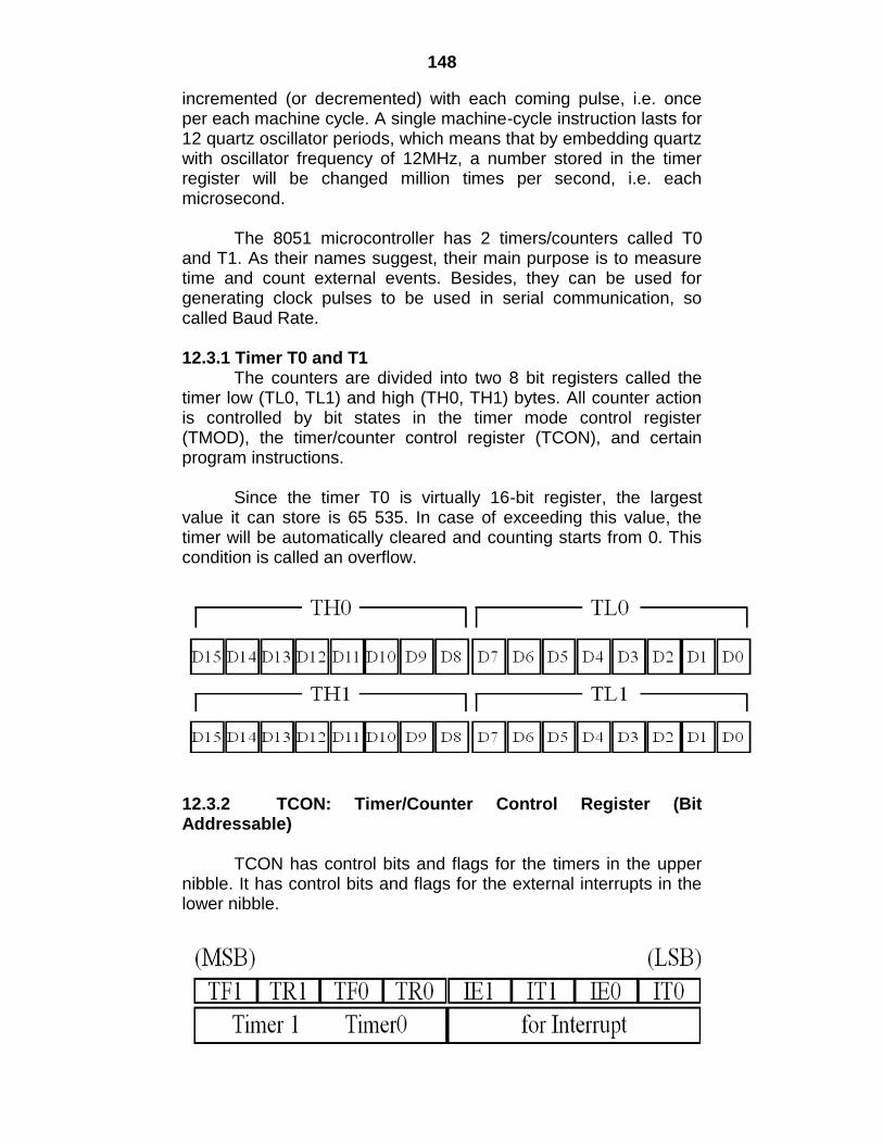
148
incremented (or decremented) with each coming pulse, i.e. once per each machine cycle. A single machine-cycle instruction lasts for 12 quartz oscillator periods, which means that by embedding quartz with oscillator frequency of 12MHz, a number stored in the timer register will be changed million times per second, i.e. each microsecond.
The 8051 microcontroller has 2 timers/counters called T0
and T1. As their names suggest, their main purpose is to measure time and count external events. Besides, they can be used for generating clock pulses to be used in serial communication, so called Baud Rate. 12.3.1 Timer T0 and T1
The counters are divided into two 8 bit registers called the timer low (TL0, TL1) and high (TH0, TH1) bytes. All counter action is controlled by bit states in the timer mode control register (TMOD), the timer/counter control register (TCON), and certain program instructions.
Since the timer T0 is virtually 16-bit register, the largest
value it can store is 65 535. In case of exceeding this value, the timer will be automatically cleared and counting starts from 0. This condition is called an overflow.
12.3.2 TCON: Timer/Counter Control Register (Bit Addressable)
TCON has control bits and flags for the timers in the upper nibble. It has control bits and flags for the external interrupts in the lower nibble.
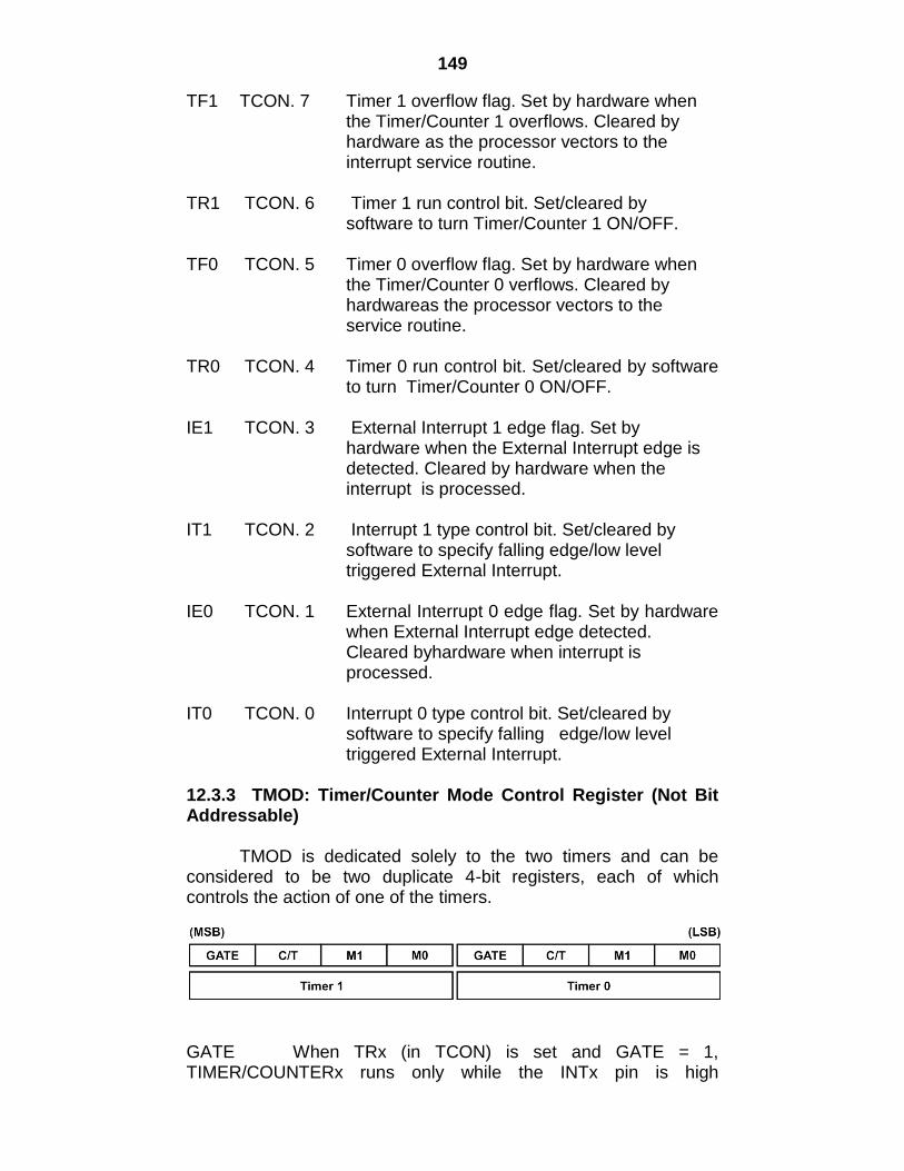
149
TF1 TCON. 7 Timer 1 overflow flag. Set by hardware when the Timer/Counter 1 overflows. Cleared by hardware as the processor vectors to the interrupt service routine.
TR1 TCON. 6 Timer 1 run control bit. Set/cleared by software to turn Timer/Counter 1 ON/OFF. TF0 TCON. 5 Timer 0 overflow flag. Set by hardware when the Timer/Counter 0 verflows. Cleared by hardwareas the processor vectors to the service routine. TR0 TCON. 4 Timer 0 run control bit. Set/cleared by software to turn Timer/Counter 0 ON/OFF. IE1 TCON. 3 External Interrupt 1 edge flag. Set by hardware when the External Interrupt edge is detected. Cleared by hardware when the interrupt is processed. IT1 TCON. 2 Interrupt 1 type control bit. Set/cleared by software to specify falling edge/low level triggered External Interrupt. IE0 TCON. 1 External Interrupt 0 edge flag. Set by hardware when External Interrupt edge detected. Cleared byhardware when interrupt is processed. IT0 TCON. 0 Interrupt 0 type control bit. Set/cleared by software to specify falling edge/low level triggered External Interrupt. 12.3.3 TMOD: Timer/Counter Mode Control Register (Not Bit Addressable)
TMOD is dedicated solely to the two timers and can be considered to be two duplicate 4-bit registers, each of which controls the action of one of the timers.
GATE When TRx (in TCON) is set and GATE = 1, TIMER/COUNTERx runs only while the INTx pin is high
150
(hardwarecontrol). When GATE = 0, TIMER/COUNTERx will run only while TRx = 1 (software control). C/T Timer or Counter selector. Cleared for Timer operation (input from internal system clock). Set for Counter operation(input from Tx input pin). M1 Mode selector bit. M0 Mode selector bit. M1 M0 Operating Mode 0 0 0 13-bit Timer 0 1 1 16-bit Timer/Counter 1 0 2 8-bit Auto-Reload Timer/Counter 1 1 3 Split Timer Mode: (Timer 0) TL0 is an 8-bit Timer/Counter controlled by the standard Timer 0control bits, TH0 is an 8-bit Timer and is controlled by Timer 1 control bits. 1 1 3 (Timer 1) Timer/Counter 1 stopped. 12.3.4 Modes of operation
TIMER MODE 0 (13 bit mode)
MODE 0 is a 13 bit mode. In this mode the THx acts as an 8 bit timer & TLx acts as a 5 bit timer. The TLx counts up to 31 & then resets to 00 & increment THx by 1. Suppose you load 0 in the timer then the timer will overflow in 213 i.e. 8192 machine cycles.
TIMER MODE 1 (16 bit mode)
MODE 1 is similar to MODE 0 except it is a 16 bit mode. In this mode the THx & TLx both acts as an 8 bit timer. The TLx counts upto 255 & then resets to 00 & increment THx by 1. Since this is a full 16 bit timer we can get maximum of 216 i.e. 65536 Machine cycle before the the timer overflows.
TIMER MODE 2 (8 bit mode)
In this Mode TLx accts as the timer & Thx contains the RELOAD VALUE i.e. THx is loaded in TLx everytime it overflows i.e. when TLx reaches 255 & is incremented then instead of resetting it to 0 it will be reseted to the value stored in THx. This mode is very commony used for generating baud rate used in serial communication.
151
TIMER MODE 3 (Split Mode)
Timers 0 and 1 may be programmed to be in mode 0, 1, or 2 independently of a similar mode for the other timer. This is not true for mode 3; the timers do not operate independently if mode 3 is chosen for timer 0. Placing timer 1 in mode 3 causes it to stop counting; the control bit TR1 and the timer 1 flag TF1 are then used by timer 0. When Timer 0 is placed in mode 3, it essentially becomes two separate 8-bit timers. That is to say, Timer 0 is TL0 and Timer 1 is TH0. Both timers count from 0 to 255 and overflow back to 0. All the bits that are related to Timer 1 will now be tied to TH0. So even if you use Timer 1 in Mode 0, 1 or 2 you won‟t be able to START or STOP the timer & no INTERRUPT will be generated by Timer 1. So the Timer 1 will be incremented every machine cycle no matter what.
12.4 SERIAL COMMUNICATION
The 8051 has a serial data communication circuit that uses register SBUF to hold the data. Register SCON controls data communication, Register PCON controls data rates, and pins RXD (P3.0) and TXD (P3.1) connect to serial network. 10.8.1 PCON – Power Control Register
D7 D6 D5 D4 D3 D2 D1 D0
SMOD x x x GF1 GF0 PD IDL
Address: 87H (not bit addressable) SMOD – Serial mode bit used to determine the baud rate with Timer 1.
If SMOD = 0 then N = 384. If SMOD = 1 then N = 192. TH1 is the high byte of timer 1 when it is in 8-bit autoreload mode. GF1 and GF0 are General purpose flags not implemented on the standard device PD is the power down bit. Not implemented on the standard device IDL activate the idle mode to save power. Not implemented on the standard device 12.4 .2 SCON – Serial Control Register The Serial Control SFR is used to configure the behavior of the 8051's on-board serial port. This SFR controls the baud rate of the
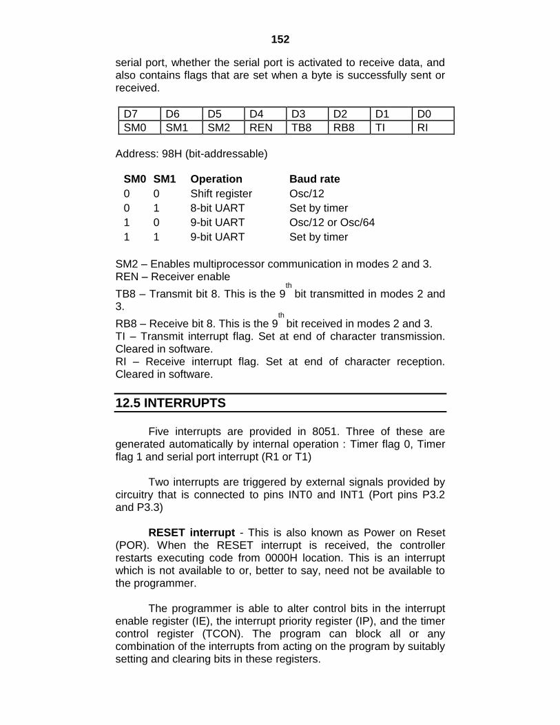
152
serial port, whether the serial port is activated to receive data, and also contains flags that are set when a byte is successfully sent or received.
D7 D6 D5 D4 D3 D2 D1 D0
SM0 SM1 SM2 REN TB8 RB8 TI RI
Address: 98H (bit-addressable)
SM0 SM1 Operation Baud rate
0 0 Shift register Osc/12
0 1 8-bit UART Set by timer
1 0 9-bit UART Osc/12 or Osc/64
1 1 9-bit UART Set by timer
SM2 – Enables multiprocessor communication in modes 2 and 3. REN – Receiver enable
TB8 – Transmit bit 8. This is the 9th
bit transmitted in modes 2 and 3.
RB8 – Receive bit 8. This is the 9th
bit received in modes 2 and 3. TI – Transmit interrupt flag. Set at end of character transmission. Cleared in software. RI – Receive interrupt flag. Set at end of character reception. Cleared in software.
12.5 INTERRUPTS
Five interrupts are provided in 8051. Three of these are
generated automatically by internal operation : Timer flag 0, Timer flag 1 and serial port interrupt (R1 or T1)
Two interrupts are triggered by external signals provided by
circuitry that is connected to pins INT0 and INT1 (Port pins P3.2 and P3.3)
RESET interrupt - This is also known as Power on Reset
(POR). When the RESET interrupt is received, the controller restarts executing code from 0000H location. This is an interrupt which is not available to or, better to say, need not be available to the programmer.
The programmer is able to alter control bits in the interrupt
enable register (IE), the interrupt priority register (IP), and the timer control register (TCON). The program can block all or any combination of the interrupts from acting on the program by suitably setting and clearing bits in these registers.
153
12.5.1 IE - Interrupt Enable register
The Interrupt Enable SFR is used to enable and disable specific interrupts. The D0 bits of the SFR are used to enable/disable the specific interrupts, where as the highest bit D7 is used to enable or disable ALL interrupts. Thus, if the high bit of IE is 0 all interrupts are disabled regardless of whether an individual interrupt is enabled by setting a lower bit.
D7 D6 D5 D4 D3 D2 D1 D0
EA x ET2 ES ET1 EX1 ET0 EX0
EA – Global interrupt enable x – not defined ET2 – Timer 2 interrupt enable ES – Serial port interrupt enable ET1 – Timer 1 interrupt enable EX1 – External interrupt 1 enable ET0 – Timer 0 interrupt enable EX0 – External interrupt 0 enable 12.5.2 IP - Interrupt Priority register
The Interrupt Priority SFR is used to specify the relative priority of each interrupt. On the 8051, an interrupt may either be of low (0) priority or high (1) priority. An interrupt may only interrupt interrupts of lower priority. For example, if we configure the 8051 so that all interrupts are of low priority except the serial interrupt, the serial interrupt will always be able to interrupt the system, even if another interrupt is currently executing. However, if a serial interrupt is executing no other interrupt will be able to interrupt the serial interrupt routine since the serial interrupt routine has the highest priority.
D7 D6 D5 D4 D3 D2 D1 D0
x x PT2 PS PT1 PX1 PT0 PX0
x – not defined PT2 – Priority for timer 2 interrupt PS – Priority for serial port interrupt PT1 – Priority for timer 1 interrupt PX1 – Priority for external interrupt 1 PT0 – Priority for timer 0 interrupt
154
PX0 – Priority for external interrupt 0
12.5 SUMMARY
The 8051 microcontroller has 2 timers/counters called T0 and
T1. They are used to measure time and count external events. Besides, they can be used for generating clock pulses to be used in serial communication.
The 8051 has a serial data communication circuit that uses
register SBUF to hold the data. Register SCON controls data communication, Register PCON controls data rates, and pins RXD (P3.0) and TXD (P3.1) connect to serial network.
Five interrupts are provided in 8051. Three of these are
generated automatically by internal operation : Timer flag 0, Timer flag 1 and serial port interrupt (R1 or T1)
Two interrupts are triggered by external signals provided by
circuitry that is connected to pins INT0 and INT1 (Port pins P3.2 and P3.3)
12.6 REVIEW QUESTIONS
Q.1 Explain the concept of SFR. Q.2 Explain the concept of timer T0 & T1. Q.3 Explain different modes of operation of timer. Q.4 Explain serial communication in 8051.
155
13
THE 8051 PORT PROGRAMMING
Unit Structure
13.1 Introduction
13.2 I/O Ports and their Functions
13.3 I/O Programming
13.4 Addressing Modes
13.5 External Data Moves
13.6 Summary
13.7 Review Questions
13.8 Reference
After studying this chapter you should be able to
Describe the I/O ports of the 8051 microcontroller.
Do the I/O programming
Understand addressing modes in 8051 programming
Understand flag register
13.1 INTRODUCTION
A Computer typically sends more time moving data from one
location to another than it spends on any other operation. Data is stored at a source address and moved to a destination address. The ways by which these addresses are specified are called the addressing modes. The 8051 mnemonics are written with the destination address named first, followed by the source address.
The 8051 microcontroller has four I/O ports. The four ports
P0, P1, P2 and P3 each use 8 pins – making them 8-bit ports. All the parts upon RESET are configured as output, ready to be used as output port. To use any of these ports as an input port, it must be programmed, as we will explain throughout this section.
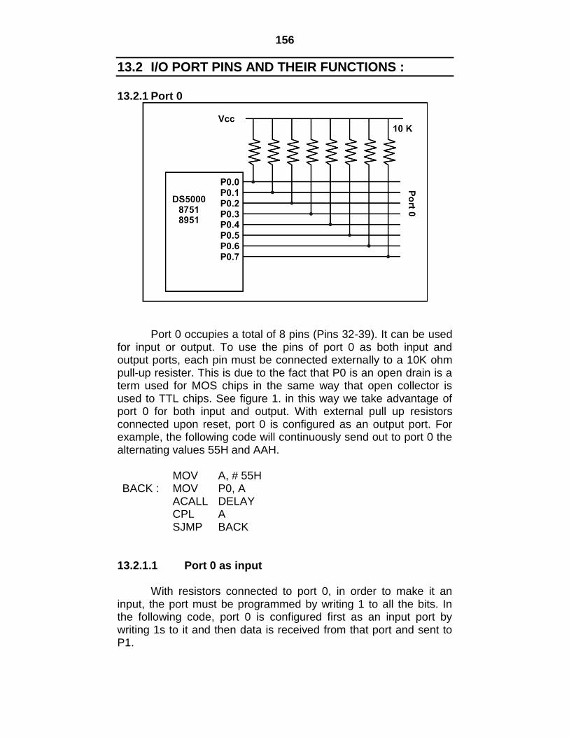
156
13.2 I/O PORT PINS AND THEIR FUNCTIONS :
13.2.1 Port 0
Port 0 occupies a total of 8 pins (Pins 32-39). It can be used for input or output. To use the pins of port 0 as both input and output ports, each pin must be connected externally to a 10K ohm pull-up resister. This is due to the fact that P0 is an open drain is a term used for MOS chips in the same way that open collector is used to TTL chips. See figure 1. in this way we take advantage of port 0 for both input and output. With external pull up resistors connected upon reset, port 0 is configured as an output port. For example, the following code will continuously send out to port 0 the alternating values 55H and AAH. MOV A, # 55H BACK : MOV P0, A ACALL DELAY CPL A SJMP BACK
13.2.1.1 Port 0 as input With resistors connected to port 0, in order to make it an input, the port must be programmed by writing 1 to all the bits. In the following code, port 0 is configured first as an input port by writing 1s to it and then data is received from that port and sent to P1.
157
MOV A, # FFH ; A = FF hex MOV P0, A ; make P0 an input port ; by writing all 1s to it BACK : MOV A, P0 ; get data from P0 MOV P1, A ; send it to port 1 SJMP BACK ; keep doing it
13.2.1.2 Dual role of port 0 As shown in figure 1, port 0 is also designated as AD0-AD7, allowing it to be used for both address and data. When connecting an 8051to an external memory, port 0 provides both address and data. The 8051 multiplexes address and data through port 0 to save pins. ALE indicates if P0 has address or data. When ALE = 0, it provides data D0-D7, but when ALE = 1 it has address A0-A7. Therefore, ALE is used for demultiplexing address and data with the help of a 74LS373 latch. 13.2.2 Port 1 Port 1 occupies a total of 8 pins (pins 1 through 8). It can be used as input or output. In contrast to port 0, this port does not need any pull-up resistors since it already has pull-up resistors internally. Upon reset port 1 is configured as an output port. For example, the following code will continuously send out to port. For example, the following code will continuously send out to port 1 the alternating values 55H and AAH. MOV A, # 55H BACK : MOV P1, A ACALL DELAY CPL A SJMP BACK
13.2.2.1 Port 1 as input To make port 1 an input port, it must programmed as such by writing 1 to all its bits. In the following code, port 1 is configured first as an input port by writing 1s to it and then data is received from that port and saved in R7, R6 and R5. MOV A, # FFH ; A = FF hex MOV P1, A ; make P1 an input port ; by writing all 1s to it MOV A, P1 ; get data from P1 MOV P7, A ; save it in reg. R7 ACALL DELAY ; Wait MOV A, P1 ; get another data from P1 MOV R6, A ; save it in reg. R6 ACALL DELAY ; Wait MOV A, P1 ; get another data from P1 MOV R6, A ; save it in reg. R5
158
13.2.3 Port 2 Port 1 occupies a total of 8 pins (pins 21 through 28). It can be used as input or output. Just like P1, port 2 does not need any pull-up resistors since it already has pull-up resistors internally. Upon reset port 2 is configured as an output port. For example, the following code will send out continuously port 2 the alternating values 55H and AAH. That is, all the bits of P2 toggle continuously. MOV A, # 55H BACK : MOV P2, A ACALL DELAY CPL A SJMP BACK
Port 2 as input To make port 1 an input port, it must programmed as such by writing 1 to all its bits. In the following code, port 1 is configured first as an input port by writing 1s to it. Then data is received from that port and is sent to P1 continuously. MOV A, # FFH ; A = FF hex MOV P2, A ; make P2 an input port ; by writing all 1s to it BACK : MOV A, P2 ; get data from P2 MOV P1, A ; send it to port 1 SJMP BACK ; keep doing it
Dual role of port 2 In 8051-based systems, port 2 must be used along with P0 to provide the 16 bit address for the external memory. As shown in figure 1, port 2 is also designated as A8-A15, indicating its dual function. Since an 8051 is capable of accessing 64 Kbytes of external memory, it needs a path for the 16 bits of the address. While P0 provides the lower 8 bits via A0-A7, it is the job of P2 to provide bits A8-A15 of the address. In other words, when the 8051 is connected to external memory, P2 is used for the upper 8 bits of the 16 bit address, and it cannot be used for I/O. We have three ports. P0, P1 and P2, for I/O operations. This should be enough for most micro controller applications. 13.2.4 Port 3 Port 3 occupies a total of 8 pins, pins 10 through 17. It can be used as input or output. P3 does not need any pull up resistors, the same as P1 and P2 did not. Although port 3 is configured as an output port upon reset, this is not the way it is most commonly used. Port 3 has the additional function of providing some
159
extremely important signals such as interrupts. Table 1 provides these alternate functions of P3. this information applies to both 8051 and 8031 chips.
P3 Bit Function Pin
P3.0 RxD 10
P3.1 TxD 11
P3.2 INT0 12
P3.3 INT1 13
P3.4 T0 14
P3.5 T1 15
P3.6 WR 16
P3.7 RD 17
P3.0 and P3.1 are used for the RxD and TxD serial communications signals. Bits P3.2 and P3.3 are set aside for external interrupts. Bits P3.4 and P3.5 are used for timers 0 and 1.
Finally P3.6 and P3.7 are used to provide the WR andRD signals of external memories connected in 8051 based systems.
13.3 I/0 PROGRAMMING; BIT MANIPULATION
In this section we further examine 8051 I/O instructions. We pay special attention to I/O bit manipulation since it is a powerful and widely used 8051 feature. 13.3.1 Different ways of Accessing the entire 8 bits In the following code, as in many previous I/O examples, the entire 8 bits of port 1 are accessed. BACK : MOV A, # 55H MOV P1, A ACALL DELAY MOV A,# AAH MOV P1, A ACALL DELAY SJMP BACK
The above code toggles even, bit of P1 continuously. We have seen a variation of the above program before. Now we can rewrite the above code in a more efficient manner by accessing the port directly without going through the accumulator. This is shown next.
160
BACK : MOV P1, # 55H ACALL DELAY MOV P1, # 55H ACALL DELAY SJMP BACK
We can write another variation of the above code by using a technique called read-modify-write. 13.3.2 Read-modify-write Feature The ports on the 8051 can be accessed by the read-modify-write technique. This feature saves many lines of code by combining in a single instruction all three actions of (1) reading the port (2) modifying it, and (3) writing to the port. The following code first places 01010101 (binary) into port 1. next, the instruction “XLR P1, # 0FFH” performs an XOR logic operation on P1 with 1111 1111 (binary) and then writes the result back into P1 MOV P1, # 55H ; P1 = 01010101 AGAIN XLR P1, # OFFH ; EX_OR P1 with 1111 1111 ACALL DELAY SJMP BACK
Notice that the XOR of 55H and FFH gives AAH. Likewise, the XOR of AAH and FFH gives 55H. 13.3.3 Single-bit addressability of ports There are times that we need to access only 1 or 2 bits of the port instead of the entire 8 bits. A powerful feature of 8051 I/O ports is their capability to access individual bits of the port without altering the rest of the bits in that port. For example, the following code toggles the bit P1.2 continuously. Back CPL P1.2 ; complement P1.2 only ACALL DELAY SJMP BACK
Another variation of the above program follows. AGAIN : SET B P1.2 ; change only P1.2 = high ACALL DELAY CPL P1.2 ; change P1.2 = low ACALL DELAY SJMP BACK
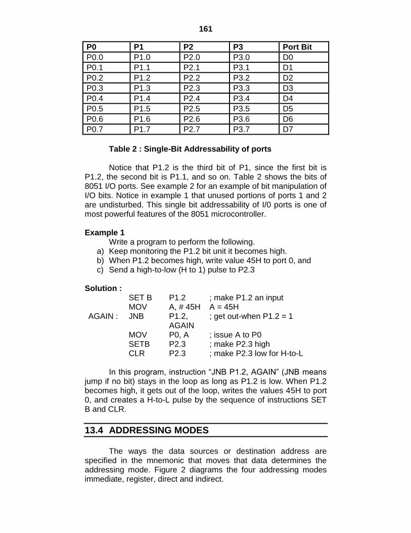
161
P0 P1 P2 P3 Port Bit
P0.0 P1.0 P2.0 P3.0 D0
P0.1 P1.1 P2.1 P3.1 D1
P0.2 P1.2 P2.2 P3.2 D2
P0.3 P1.3 P2.3 P3.3 D3
P0.4 P1.4 P2.4 P3.4 D4
P0.5 P1.5 P2.5 P3.5 D5
P0.6 P1.6 P2.6 P3.6 D6
P0.7 P1.7 P2.7 P3.7 D7
Table 2 : Single-Bit Addressability of ports
Notice that P1.2 is the third bit of P1, since the first bit is P1.2, the second bit is P1.1, and so on. Table 2 shows the bits of 8051 I/O ports. See example 2 for an example of bit manipulation of I/O bits. Notice in example 1 that unused portions of ports 1 and 2 are undisturbed. This single bit addressability of I/0 ports is one of most powerful features of the 8051 microcontroller. Example 1 Write a program to perform the following.
a) Keep monitoring the P1.2 bit unit it becomes high. b) When P1.2 becomes high, write value 45H to port 0, and c) Send a high-to-low (H to 1) pulse to P2.3
Solution : SET B P1.2 ; make P1.2 an input MOV A, # 45H A = 45H AGAIN : JNB P1.2,
AGAIN ; get out-when P1.2 = 1
MOV P0, A ; issue A to P0 SETB P2.3 ; make P2.3 high CLR P2.3 ; make P2.3 low for H-to-L
In this program, instruction “JNB P1.2, AGAIN” (JNB means jump if no bit) stays in the loop as long as P1.2 is low. When P1.2 becomes high, it gets out of the loop, writes the values 45H to port 0, and creates a H-to-L pulse by the sequence of instructions SET B and CLR.
13.4 ADDRESSING MODES
The ways the data sources or destination address are specified in the mnemonic that moves that data determines the addressing mode. Figure 2 diagrams the four addressing modes immediate, register, direct and indirect.
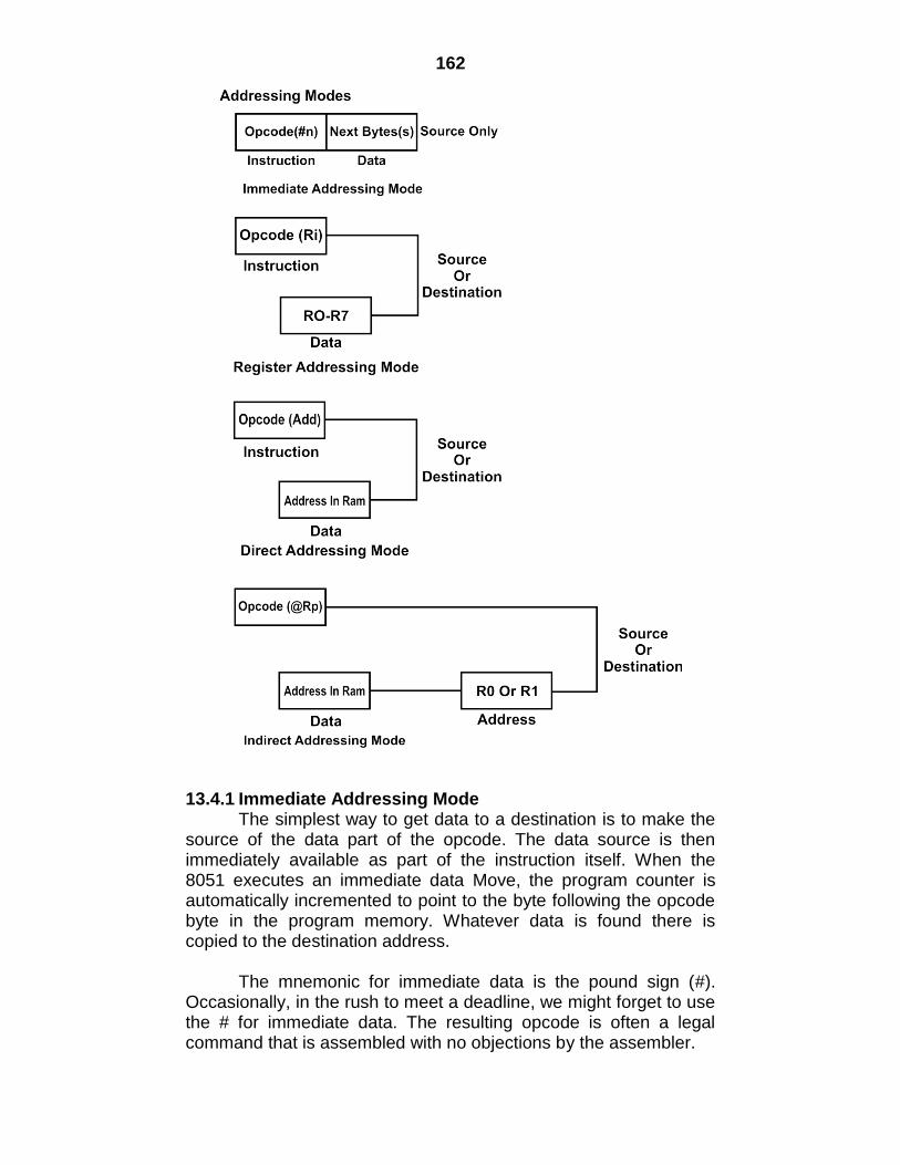
162
13.4.1 Immediate Addressing Mode The simplest way to get data to a destination is to make the source of the data part of the opcode. The data source is then immediately available as part of the instruction itself. When the 8051 executes an immediate data Move, the program counter is automatically incremented to point to the byte following the opcode byte in the program memory. Whatever data is found there is copied to the destination address. The mnemonic for immediate data is the pound sign (#). Occasionally, in the rush to meet a deadline, we might forget to use the # for immediate data. The resulting opcode is often a legal command that is assembled with no objections by the assembler.
163
13.4.2 Register Addressing Mode Certain register names may be used as part of the opcode mnemonic as sources or destinations of data. Registers A DPTR, and R0 to R7 may be named as part of the opcode mnemonic. Other registers in the 8051 may be addressed using the direct addressing mode. Remember that the registers used in the opcode as R0 to R7 are the ones that are currently chosen by the blank-select bits, RS0 and RS1 in the PSW.
The following table shows all possible MOVopcodes using immediate and register addressing modes.
Mnemonic Operation
MOV A, #n Copy the immediate data byte n to the A register
MOV A, Rr Copy data from Rr to the A register
MOV Rr, A Copy data from A to the Rr register
MOV Rr, #n Copy the immediate data byte n to Rr register
MOV DPTR, #nn
Copy the immediate 16 bit number nn to the DPTR register
A data MOV does not alter the contents of the data source address. A copy of the data is made from the source and Moved to the destination address the contents of the destination address are replaced by the source address contents the following table shows examples of MOVopcodes with immediate and register addressing modes.
Mnemonic Operation
MOV A, #0F1n Move the immediate data byte F1h to the A register
MOV A, R0 Copy the data in register R0 to register A
MOV DPTR, # 0ABCDh
Move the immediate data bytes ABCDh to the DPTR
MOV R5, a Copy the data in register A to register R5
MOV R3, #1Ch
Move the immediate data byte 1Ch to register R3
13.4.3 Direct Addressing Mode All 128 bytes of internal RAM and the SFRS may be a addressed directly using the single-byte address assigned to each RAM location and each special function register. Internal RAM uses addresses from ooh to 7Fh to address each byte. The SFR addresses exist from 80h to FFh at the following locations.
SFR ADDRESS (HEX)
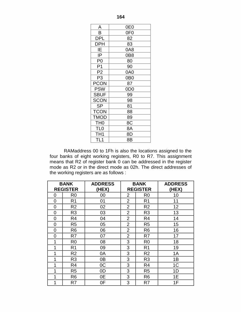
164
A 0E0
B 0F0
DPL 82
DPH 83
IE 0A8
IP 0B8
P0 80
P1 90
P2 0A0
P3 0B0
PCON 87
PSW 0D0
SBUF 99
SCON 98
SP 81
TCON 88
TMOD 89
TH0 8C
TL0 8A
TH1 8D
TL1 8B
RAMaddress 00 to 1Fh is also the locations assigned to the four banks of eight working registers, R0 to R7. This assignment means that R2 of register bank 0 can be addressed in the register mode as R2 or in the direct mode as 02h. The direct addresses of the working registers are as follows :
BANK REGISTER
ADDRESS (HEX)
BANK REGISTER
ADDRESS (HEX)
0 R0 00 2 R0 10
0 R1 01 2 R1 11
0 R2 02 2 R2 12
0 R3 03 2 R3 13
0 R4 04 2 R4 14
0 R5 05 2 R5 15
0 R6 06 2 R6 16
0 R7 07 2 R7 17
1 R0 08 3 R0 18
1 R1 09 3 R1 19
1 R2 0A 3 R2 1A
1 R3 0B 3 R3 1B
1 R4 0C 3 R4 1C
1 R5 0D 3 R5 1D
1 R6 0E 3 R6 1E
1 R7 0F 3 R7 1F
165
Only one bank of working registers is active at any given time. The PSW special-function register holds the bank-select bits, RS0 and RS1, which determine which register bank is in use. When the 8051 is reset, RS0 and RS1 are set to 006 to select the working registers in bank 0, located from 00h to 07h in internal RAM. Reset also sets SP to 07h, and the stack will grow up as it is used. This growing stack will overwrite the register banks above bank 0 be sure to set the SP to a number above those of any working registers the program may use. The programmer may choose any other bank by setting RS0 and RS1 as desired; this bank change is often done to “save” one bank and choose another when servicing an interrupt or using a subroutine. The programmer may elect to use the absolute numeric address number for an SFR or may use a symbol (name) for the SFR. For example, the following instructions both Move a constant number into port 1:
MOV 90h, #0A5h MOV P1, #0A5h The A51 assembler, supplied with this book, “looks up” the actual address of an SFR when the programmer uses an SFR symbol. We shall use both methods of specifying SFRS in this to emphasize the fact that SFRS are internal RAM addresses. The Moves made possible using direct, immediate and register addressing modes are as follows :
Mnemonic Operation
MOV A, add Copy data from direct address add to register A
MOV add, A Copy data from register A to direct address add
MOV Rr, add Copy data from direct address add to register Rr
MOV add, Rr Copy data from register Rr to direct address add
MOV add, #n Copy immediate data byte n to direct address add
MOV add 1, add 2
Copy data from direct address add2 to direct address add 1
166
The following table show example of MOV opcodes using direct, immediate, and registers addressing modes:
Mnemonic Operation
MOV A, 80h Copy data from the port 0 pins to register
MOV 80h, A Copy data from register A to the port 0 latch
MOV 3Ah, #3Ah Copy immediate data byte 3Ah to RAM location 3Ah
MOV R0, 12h Copy data from RAM location 12h to register R0
MOV 8Ch, R7 Copy data from register R7 to timer 0 high byte
MOV 5Ch, A Copy data from register A to RAM location 5Ch
MOV 0a8h, 77h Copy data from RAM location 77h to IE register
13.4.4 Indirect Addressing Mode For all the addressing modes covered to this point. The sources or destination of the data is an absolute number or a name. Inspection of the opcode reveals exactly what the address are of the destination and source. For example, the opcodeMOV A, RT say that the A register will get a copy of whatever data is in register R7; MOV 33h, # 32h Moves the hex number 32 to hex RAM address 33. The indirect addressing mode uses a register to hold the actual address that will finally be used in the data Move; the register itself is not the address, but rather the number in the register. Indirect addressing for MOVopcodes uses register R0 to R1; often called a data pointer, to hold the address of one of the data locations in RAM from address ooh to 7fh. The number that is in the pointing register (Rp) cannot be known unless the history of the register is known. The mnemonic symbol used for indirect addressing is the “act” sign, which is printed as @. The Moves made possible using immediate, direct, register, and indirect modes are as follows :
Mnemonic Operation
MOV @Rp, #n Copy the immediate byte n to the address in Rp
MOV @Rp, add Copy the contents of add to the address in Rp
MOV @Rp, A Copy the data in A to the address in Rp
MOV add, @ Rp Copy the contents of the address in Rp to add
MOV add, @ Rp Copy the contents of the address in Rp to A
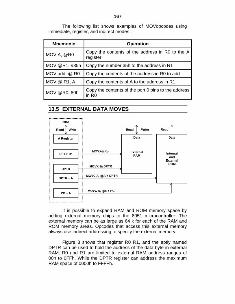
167
The following list shows examples of MOVopcodes using immediate, register, and indirect modes :
Mnemonic Operation
MOV A, @R0 Copy the contents of the address in R0 to the A register
MOV @R1, #35h Copy the number 35h to the address in R1
MOV add, @ R0 Copy the contents of the address in R0 to add
MOV @ R1, A Copy the contents of A to the address in R1
MOV @R0, 80h Copy the contents of the port 0 pins to the address in R0
13.5 EXTERNAL DATA MOVES
It is possible to expand RAM and ROM memory space by adding external memory chips to the 8051 microcontroller. The external memory can be as large as 64 k for each of the RAM and ROM memory areas. Opcodes that access this external memory always use indirect addressing to specify the external memory. Figure 3 shows that register R0 R1, and the aptly named DPTR can be used to hold the address of the data byte in external RAM. R0 and R1 are limited to external RAM address ranges of 00h to 0FFh. While the DPTR register can address the maximum RAM space of 0000h to FFFFh.
168
An X is added to the MOV mnemonic to serve as a reminder that the data move external to 8051.
Mnemonic Operation
MOVX A, @Rp Copy the contents of the external address in Rp to A
MOVX A, @ DPTR Copy the contents of the external address in DPTR to A
MOVX, @ Rp, A Copy data from A to the external address in Rp
MOVX, @ DPTR, A Copy data from A to the external address in DPTR
Code Memory Read Only Moves There are times when access to a preprogrammed mass of data is needed, such as when using tables of predefined bytes. This data must be permanent to be of repeated use and is stored in the program ROM. Access to this data is made possible by using indirect addressing and A register in conjunction with either the PC or DPTR, as shown in fig. In both cases, the number in register A is added to the pointing register to form the ROM address so formed and placed in the A register. The original data in A lost, and the addressed data takes its place. The letter C is added to the MOV mnemonic to highlight the use of opcodes for moving data from the source address in the code ROM to the A register in the 8051
Mnemonic Operation
MOVC A,@A + DPTR
Copy the code byte, found at the ROM address formed by adding A and the DPTR to A
MOVC A, @ A + PC
Copy the code byte, found at the ROM address formed by adding A and the PC to A
The DPTR and PC are not changed; the A register contains the ROM byte found at the address formed. The following table shows example of code ROM moves using register and indirect addressing modes :
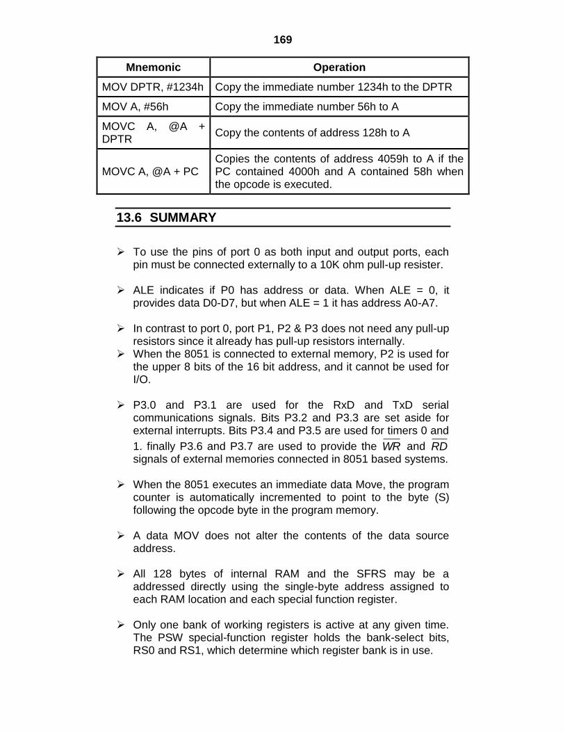
169
Mnemonic Operation
MOV DPTR, #1234h Copy the immediate number 1234h to the DPTR
MOV A, #56h Copy the immediate number 56h to A
MOVC A, @A + DPTR
Copy the contents of address 128h to A
MOVC A, @A + PC Copies the contents of address 4059h to A if the PC contained 4000h and A contained 58h when the opcode is executed.
13.6 SUMMARY
To use the pins of port 0 as both input and output ports, each pin must be connected externally to a 10K ohm pull-up resister.
ALE indicates if P0 has address or data. When ALE = 0, it
provides data D0-D7, but when ALE = 1 it has address A0-A7. In contrast to port 0, port P1, P2 & P3 does not need any pull-up
resistors since it already has pull-up resistors internally. When the 8051 is connected to external memory, P2 is used for
the upper 8 bits of the 16 bit address, and it cannot be used for I/O.
P3.0 and P3.1 are used for the RxD and TxD serial
communications signals. Bits P3.2 and P3.3 are set aside for external interrupts. Bits P3.4 and P3.5 are used for timers 0 and
1. finally P3.6 and P3.7 are used to provide the WR and RD signals of external memories connected in 8051 based systems.
When the 8051 executes an immediate data Move, the program
counter is automatically incremented to point to the byte (S) following the opcode byte in the program memory.
A data MOV does not alter the contents of the data source
address. All 128 bytes of internal RAM and the SFRS may be a
addressed directly using the single-byte address assigned to each RAM location and each special function register.
Only one bank of working registers is active at any given time.
The PSW special-function register holds the bank-select bits, RS0 and RS1, which determine which register bank is in use.
170
The mnemonic symbol used for indirect addressing is the “act” sign, which is printed as @.
The 8051 has four arithmetic flags : the carry (c), Auxiliary carry
(AC), over flow (OV), and parity (P).
13.7 REVIEW QUESTIONS
Q.1 Explain Port 0 in detail. Q.2 Explain the Dual role of Port 0. Q.3 Explain Port 1 in detail. Q.4 Explain Port 2 in detail. Q.5 Explain Port 3 in detail. Q.6 Explain different addressing modes in 8051 with two
examples of each. Q.7 Explain immediate addressing mode in 8051 in detail. Q.8 Explain direct addressing mode in 8051 in detail. Q.7 Explain indirect addressing mode in 8051 in detail.
13.8 REFERENCE
The 8051 Microcontroller by Kenneth J. Ayala, Publisher:
Thomson Delmar Learning The 8051 Microcontroller And Embedded Systems Using
Assembly And C, 2/E By Mazidi and Mazidi, Publisher: Pearson Education India
171
14
ARITHMETIC & LOGICAL OPERATION
Unit Structure
14.1 Introduction
14.2 Flags
14.3 Incrementing and Decrementing
14.4 Addition
14.5 Subtraction
14.6 Multiplication and Division
14.7 Decimal Arithmetic
14.8 Logical Instructions
14.9 Internal RAM Bit Addresses
14.10 SFR Bit Addresses
14.11 Bit – Level Boolean Operations
14.12Rotate and Swap Operations
14.13 Summary
14.14 Review Question
14.15 Reference After studying this chapter you should be able to Understand addition, subtraction, multiplication and division Understand the logic of programs Do the assembly language programming Understand bit level Boolean operation
14.1 INTRODUCTION
Applications of microcontrollers often involve performing
mathematical calculations on the data in order to alter program flow and modify program actions. The domain of the microcontroller is that of controlling events as they change. A sufficient number of mathematical opcodes must be provided, so that calculations associated with the control of simple processes can be done.
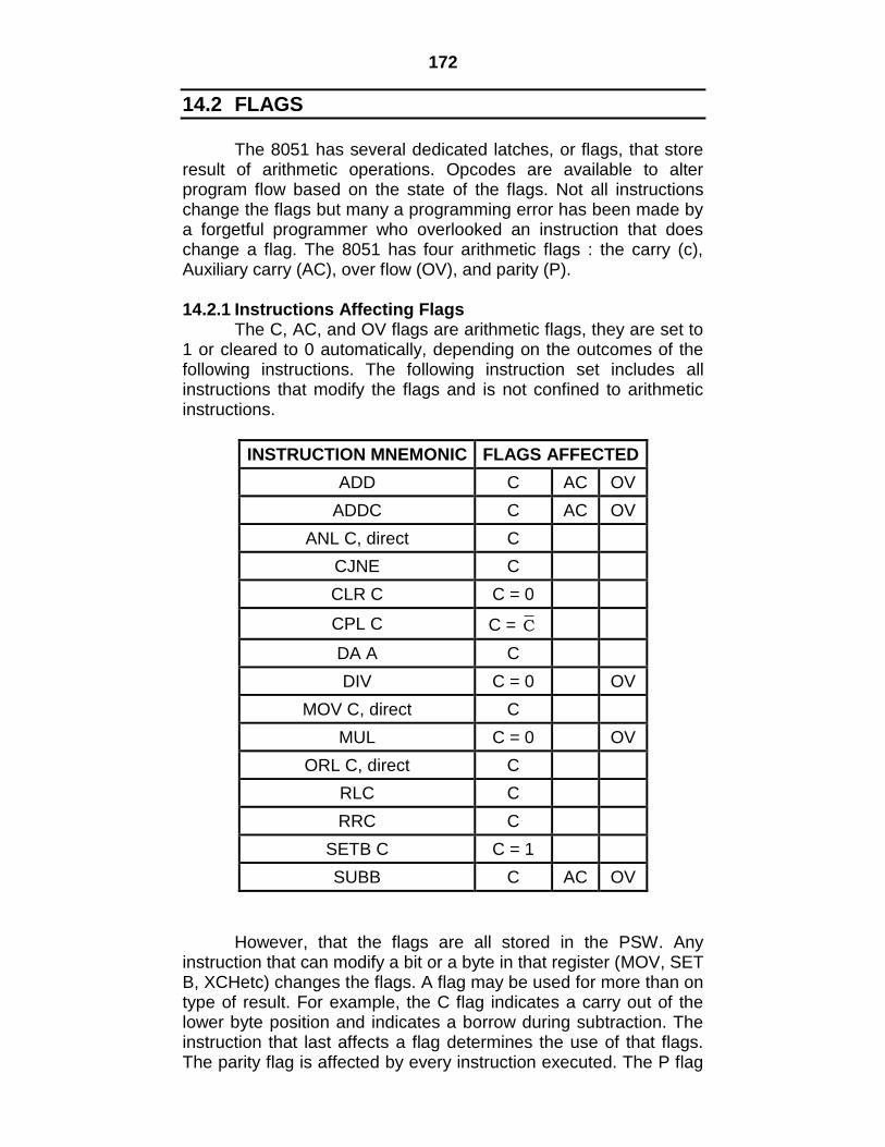
172
14.2 FLAGS
The 8051 has several dedicated latches, or flags, that store result of arithmetic operations. Opcodes are available to alter program flow based on the state of the flags. Not all instructions change the flags but many a programming error has been made by a forgetful programmer who overlooked an instruction that does change a flag. The 8051 has four arithmetic flags : the carry (c), Auxiliary carry (AC), over flow (OV), and parity (P). 14.2.1 Instructions Affecting Flags The C, AC, and OV flags are arithmetic flags, they are set to 1 or cleared to 0 automatically, depending on the outcomes of the following instructions. The following instruction set includes all instructions that modify the flags and is not confined to arithmetic instructions.
INSTRUCTION MNEMONIC FLAGS AFFECTED
ADD C AC OV
ADDC C AC OV
ANL C, direct C
CJNE C
CLR C C = 0
CPL C C = C
DA A C
DIV C = 0 OV
MOV C, direct C
MUL C = 0 OV
ORL C, direct C
RLC C
RRC C
SETB C C = 1
SUBB C AC OV
However, that the flags are all stored in the PSW. Any instruction that can modify a bit or a byte in that register (MOV, SET B, XCHetc) changes the flags. A flag may be used for more than on type of result. For example, the C flag indicates a carry out of the lower byte position and indicates a borrow during subtraction. The instruction that last affects a flag determines the use of that flags. The parity flag is affected by every instruction executed. The P flag
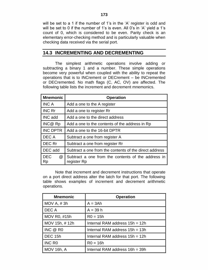
173
will be set to a 1 if the number of 1‟s in the „A‟ register is odd and will be set to 0 if the number of 1‟s is even. All 0‟s in „A‟ yield a 1‟s count of 0, which is considered to be even. Parity check is an elementary error-checking method and is particularly valuable when checking data received via the serial port.
14.3 INCREMENTING AND DECREMENTING
The simplest arithmetic operations involve adding or subtracting a binary 1 and a number. These simple operations become very powerful when coupled with the ability to repeat the operations that is to INCrement or DECrement – be INCremented or DECremented. No math flags (C, AC, OV) are affected. The following table lists the increment and decrement mnemonics.
Mnemonic Operation
INC A Add a one to the A register
INC Rr Add a one to register Rr
INC add Add a one to the direct address
INC@ Rp Add a one to the contents of the address in Rp
INC DPTR Add a one to the 16-bit DPTR
DEC A Subtract a one from register A
DEC Rr Subtract a one from register Rr
DEC add Subtract a one from the contents of the direct address
DEC @ Rp
Subtract a one from the contents of the address in register Rp
Note that increment and decrement instructions that operate on a port direct address alter the latch for that port. The following table shows examples of increment and decrement arithmetic operations.
Mnemonic Operation
MOV A, # 3h A = 3Ah
DEC A A = 39 h
MOV R0, #15h R0 = 15h
MOV 15h, # 12h Internal RAM address 15h = 12h
INC @ R0 Internal RAM address 15h = 13h
DEC 15h Internal RAM address 15h = 12h
INC R0 R0 = 16h
MOV 16h, A Internal RAM address 16h = 39h
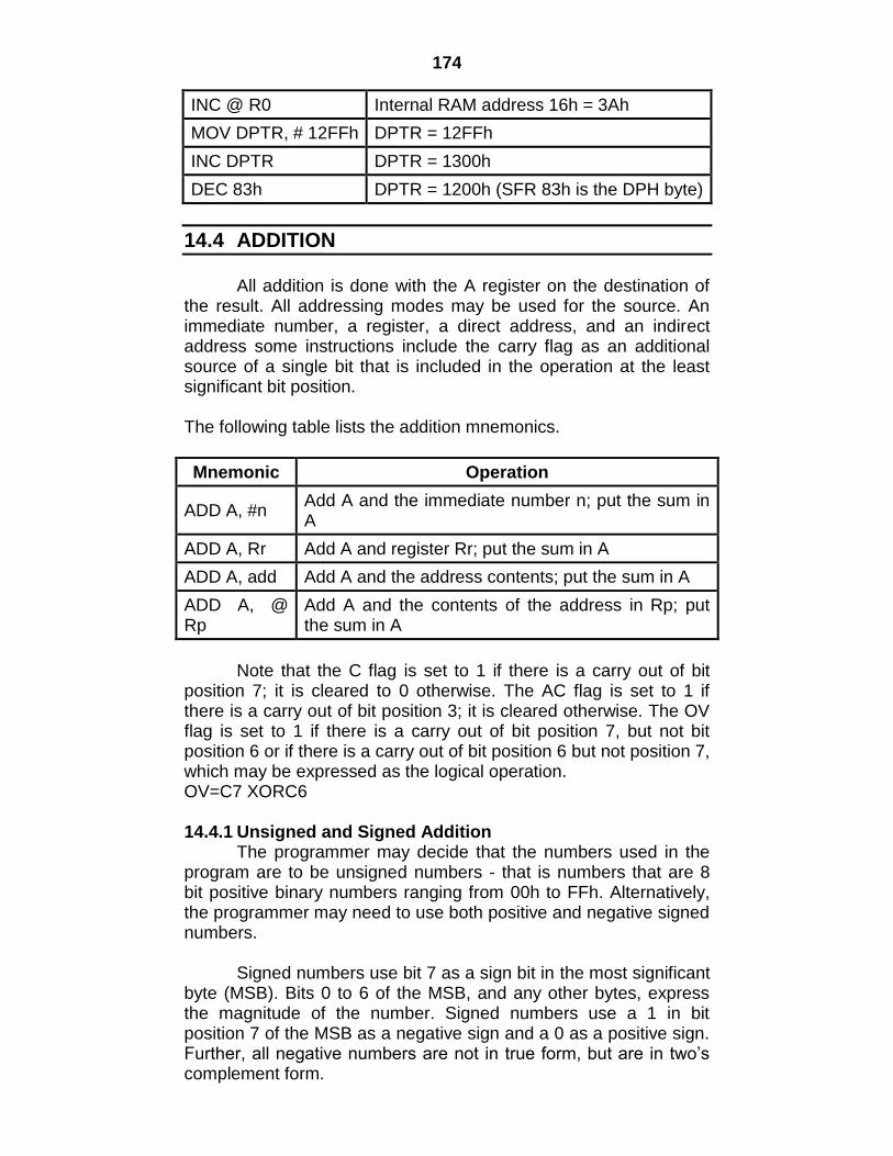
174
INC @ R0 Internal RAM address 16h = 3Ah
MOV DPTR, # 12FFh DPTR = 12FFh
INC DPTR DPTR = 1300h
DEC 83h DPTR = 1200h (SFR 83h is the DPH byte)
14.4 ADDITION
All addition is done with the A register on the destination of the result. All addressing modes may be used for the source. An immediate number, a register, a direct address, and an indirect address some instructions include the carry flag as an additional source of a single bit that is included in the operation at the least significant bit position. The following table lists the addition mnemonics.
Mnemonic Operation
ADD A, #n Add A and the immediate number n; put the sum in A
ADD A, Rr Add A and register Rr; put the sum in A
ADD A, add Add A and the address contents; put the sum in A
ADD A, @ Rp
Add A and the contents of the address in Rp; put the sum in A
Note that the C flag is set to 1 if there is a carry out of bit position 7; it is cleared to 0 otherwise. The AC flag is set to 1 if there is a carry out of bit position 3; it is cleared otherwise. The OV flag is set to 1 if there is a carry out of bit position 7, but not bit position 6 or if there is a carry out of bit position 6 but not position 7, which may be expressed as the logical operation. OV=C7 XORC6 14.4.1 Unsigned and Signed Addition The programmer may decide that the numbers used in the program are to be unsigned numbers - that is numbers that are 8 bit positive binary numbers ranging from 00h to FFh. Alternatively, the programmer may need to use both positive and negative signed numbers. Signed numbers use bit 7 as a sign bit in the most significant byte (MSB). Bits 0 to 6 of the MSB, and any other bytes, express the magnitude of the number. Signed numbers use a 1 in bit position 7 of the MSB as a negative sign and a 0 as a positive sign. Further, all negative numbers are not in true form, but are in two‟s complement form.
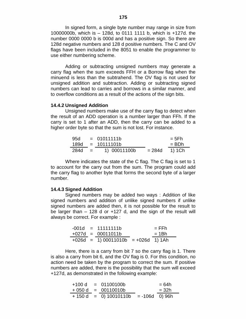
175
In signed form, a single byte number may range in size from 10000000b, which is – 128d, to 0111 1111 b, which is +127d. the number 0000 0000 b is 000d and has a positive sign. So there are 128d negative numbers and 128 d positive numbers. The C and OV flags have been included in the 8051 to enable the programmer to use either numbering scheme. Adding or subtracting unsigned numbers may generate a carry flag when the sum exceeds FFH or a Borrow flag when the minuend is less than the subtrahend. The OV flag is not used for unsigned addition and subtraction. Adding or subtracting signed numbers can lead to carries and borrows in a similar manner, and to overflow conditions as a result of the actions of the sign bits. 14.4.2 Unsigned Addition Unsigned numbers make use of the carry flag to detect when the result of an ADD operation is a number larger than FFh. If the carry is set to 1 after an ADD, then the carry can be added to a higher order byte so that the sum is not lost. For instance.
95d = 01011111b = 5Fh 189d = 10111101b = BDh
284d = 1) 00011100b = 284d 1) 1Ch Where indicates the state of the C flag. The C flag is set to 1 to account for the carry out from the sum. The program could add the carry flag to another byte that forms the second byte of a larger number. 14.4.3 Signed Addition Signed numbers may be added two ways : Addition of like signed numbers and addition of unlike signed numbers if unlike signed numbers are added then, it is not possible for the result to be larger than – 128 d or +127 d, and the sign of the result will always be correct. For example :
-001d = 11111111b = FFh +027d = 00011011b = 1Bh
+026d = 1) 00011010b = +026d 1) 1Ah Here, there is a carry from bit 7 so the carry flag is 1. There is also a carry from bit 6, and the OV flag is 0. For this condition, no action need be taken by the program to correct the sum. If positive numbers are added, there is the possibility that the sum will exceed +127d, as demonstrated in the following example:
+100 d = 01100100b = 64h + 050 d = 00110010b = 32h
+ 150 d = 0) 10010110b = -106d 0) 96h
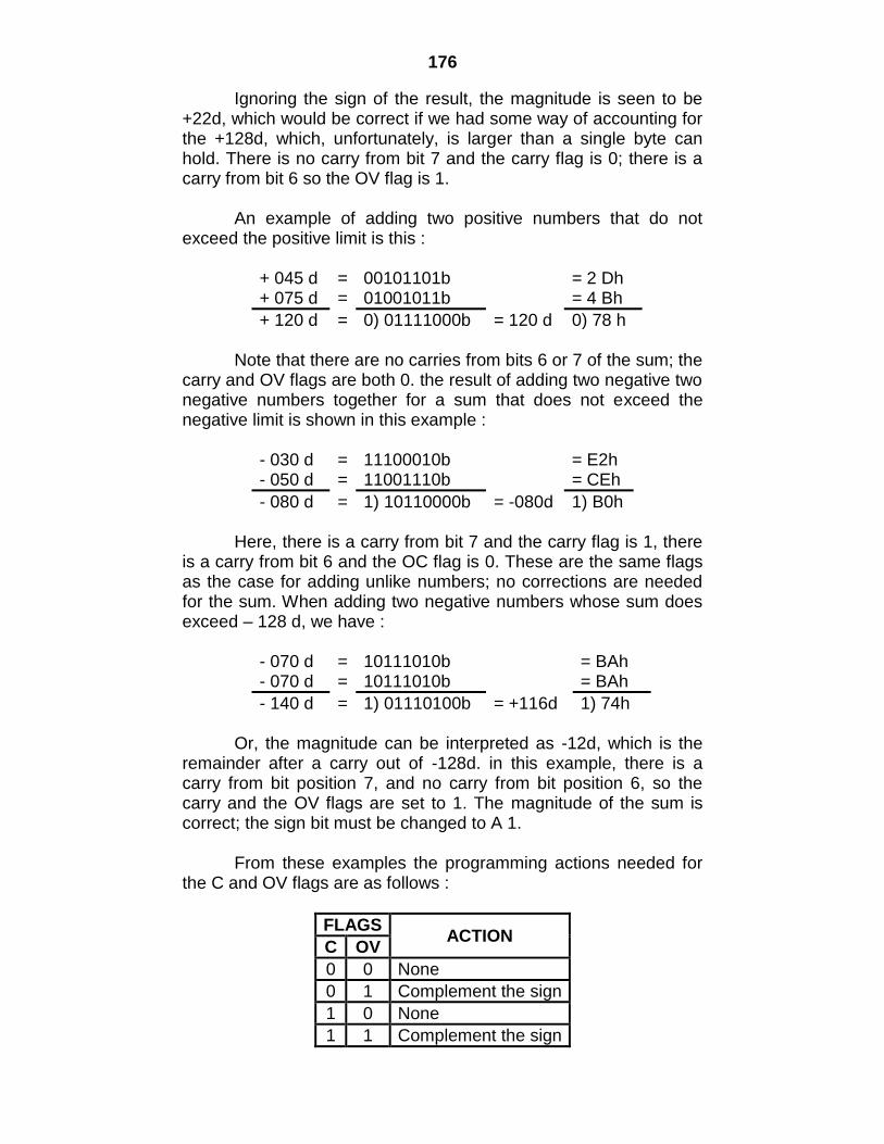
176
Ignoring the sign of the result, the magnitude is seen to be +22d, which would be correct if we had some way of accounting for the +128d, which, unfortunately, is larger than a single byte can hold. There is no carry from bit 7 and the carry flag is 0; there is a carry from bit 6 so the OV flag is 1. An example of adding two positive numbers that do not exceed the positive limit is this :
+ 045 d = 00101101b = 2 Dh + 075 d = 01001011b = 4 Bh
+ 120 d = 0) 01111000b = 120 d 0) 78 h Note that there are no carries from bits 6 or 7 of the sum; the carry and OV flags are both 0. the result of adding two negative two negative numbers together for a sum that does not exceed the negative limit is shown in this example :
- 030 d = 11100010b = E2h - 050 d = 11001110b = CEh
- 080 d = 1) 10110000b = -080d 1) B0h Here, there is a carry from bit 7 and the carry flag is 1, there is a carry from bit 6 and the OC flag is 0. These are the same flags as the case for adding unlike numbers; no corrections are needed for the sum. When adding two negative numbers whose sum does exceed – 128 d, we have :
- 070 d = 10111010b = BAh - 070 d = 10111010b = BAh
- 140 d = 1) 01110100b = +116d 1) 74h Or, the magnitude can be interpreted as -12d, which is the remainder after a carry out of -128d. in this example, there is a carry from bit position 7, and no carry from bit position 6, so the carry and the OV flags are set to 1. The magnitude of the sum is correct; the sign bit must be changed to A 1. From these examples the programming actions needed for the C and OV flags are as follows :
FLAGS ACTION
C OV
0 0 None
0 1 Complement the sign
1 0 None
1 1 Complement the sign
177
A general rule is that if the OV flag is set and then complement the sign. The OV flag also signals that the sum exceeds the largest positive or negative numbers thought to be needed in the program. 14.4.4 Multiple – Byte Signed Arithmetic The nature of multiple – byte arithmetic for signed and unsigned numbers is distinctly different from single – byte arithmetic. Using more than one byte in unsigned arithmetic means that carries or borrows are propagated from low-order to high order bytes by the simple technique of adding the carry to the next highest byte for addition and subtracting the borrow from the next highest byte for subtraction. Signed numbers appear to behave like unsigned numbers until the last byte is reached. For a signed numbers the seventh bit of the highest byte is the sign; if the sign is negative, then the entire number is in two‟s complement form. For example, using a 2-byte signed number we have the following examples :
+ 32767 d = 01111111 11111111 b = 7FFFh + 00000 d = 00000000 00000000b = 0000 h - 00001 d = 11111111 11111111 b = FFFFh
- 32768 d = 10000000 00000000 b = 80000 h Note that the lowest byte of the numbers 00000 d and -32768 d are exactly alike, as are the lowest bytes for +32767 d and -00001 d. For multi-byte signed number arithmetic, then, the lower bytes are treated as unsigned numbers. All checks for overflow are done only for the highest order byte that contains the sign. An overflow at the highest order byte is not usually recoverable. The programmer has made a mistake and probably has made no provisions for a number larger than planned. Some error acknowledgement procedure, or user notification, should be included in the program if this type of mistake is a possibility. The preceding examples show the need to add the carry flag to higher order bytes in signed and unsigned addition operations. Opcodes that accomplish this task are similar to the ADD mnemonics. A C is appended to show that the carry bit is added to the sum in bit position 0.
178
The following table lists the add with carry mnemonics :
Mnemonic Operation
ADDC A. #n Add the contents of A, the immediate number n and C flag; put the sum in A
ADDC A, add
Add the contents of A. the direct address contents, and the C flag; put the sum in A
ADDC A, Rr Add the contents of A, register Rr, and the C flag; put the sum in A
ADDC A, @Rp
Add the contents of A. the contents of the indirect address in Rp, and the C flag; put the sum in A
Note that the AC and OV flags behave exactly as they do for the ADD commands. The following table shows examples of ADD and ADDC multiple byte signed arithmetic operations.
Mnemonic Operation
MOV A,# 1Ch A = 1 Ch
MOV R5, # 0A 1h R5 = A 1h
ADD A, R5 A = BDh; C = 0, OV = 0
ADD A, R5 A = 5Eh; C = 1, OV = 1
ADD A, # 10h A = 6Fh; C = 0, OV = 0
ADD A, # 10h A = 7Fh; C = 0, OV = 0
14.5 SUBTRACTION
Subtraction can be done by taking the two‟s complement of the number to be subtracted, the subtrahend, and adding it to another number, the minuend. The 8051, however, has commands to perform direct subtraction of two signed or unsigned numbers. Register A is the destination address for subtraction. All four addressing modes may be used for source addresses. The commands treat the carry flag as a borrow and always subtract the carry flat as part of the operation.
179
The following table lists the subtract mnemonics :
Mnemonic Operation
SUBB A, #n Subtract immediate number n and the C flag from A; put the result in A
SUBB A, add Subtract the contents of add and the C flag from A; put the result in A
SUBB A, Rr Subtract Rr and the C flag from A; put the result in A
SUBB A, @ Rp Subtract the contents of the address In Rp and the C flag from A; put the result in A
Note that the C flag is set if a borrow is needed into bit 7 and reset otherwise. The AC flag is set if a borrow is needed into bit 3 and reset otherwise. The OV flag is set if there is a borrow into bit 7 and not bit 6 or if there is a borrow into bit 6 and bit 7. As in the case for addition, the OV flag is the XOR of the borrows into bit positions 7 and 6.
14.5.1 Unsigned and Signed Subtraction Again, depending on what is needed, the programmer may choose to use bytes as signed or unsigned numbers. The carry flag is now thought of as a Borrow flag to account for situations when a larger number is subtracted form a smaller number. The OV flag indicates results that must be adjusted whenever two numbers of unlike signs one subtracted and the result exceeds the planned signed magnitudes. 14.5.2 Unsigned Subtraction Because the C flag is always subtracted from A along with the source byte, it must be set to 0 if the programmer does not want the flag included in the subtraction. If a multi – byte subtraction is done the C flag is cleared for the first byte and then included in subsequent higher byte operations.
The result will be in true form, with no borrow if the source number is smaller than A, or in two‟s complement form, with a borrow if the source is larger than A. these are not signed number as all 8 bits are used for the magnitude. The range of numbers is from positive 255 d (c = 0, A = FFh) to negative 255 d (C = 1, A = 01h).
The following example demonstrates subtraction of a larger number from a smaller number.
015 d = 0000 1111 b = 0Fh SUB B 100 d = 011 00 100 b = 64 h
- 085 d 1) 10101011 b = 171 h = 1) ABh
180
The C flag is set to 1, and the OV flag is set to 0. The two‟s complement of the result is 085 d. The reverse of the example yields the following result :
100 d = 01100100 b = 64 h0Fh SUB B 115 d = 00000000 b = OFh
- 085 d 0) 01010101 b = 085 d 0) 55h The C flag is set to 0, and the OV flag is set 0. the magnitude of the result is in true form 14.5.3 Signed Subtraction As is the case for addition two combinations of unsigned numbers are possible when subtracting: subtracting numbers of like and unlike signs. When number of like sign are subtracted, it is impossible for the result to exceed positive or negative magnitude limits of + 127 d or – 128 d, so the magnitude and sign of the result do not need to be adjusted, as shown in the following example :
+ 100 d = 01100100b (carry flag = 0 before SUB B)
= 64 h
SUB B + 126 d = 01111110b = 7E h
- 026 d 1) 11100110b = 085 d DE6h There is a borrow into bit positions 7 and 6; the carry flag is set to 1, and the OV flag is cleaned. The following example demonstrates using two negative numbers.
- 61 d = 11000011 b (carry flag = 0 before SUB B)
= C3 h
SUB B - 116 d = 10001100b = 8 C h
+ 055 d 0) 00110111 b = 055 d DE6h There are no borrows into bit positions 6 or 7, so the OV and carry flags are cleared to 0. An overflow is possible when subtracting numbers of opposite sign because the situation becomes one of adding numbers of like signs, as can be demonstrated in the following example : - 099 d = 10011101 b (carry flag = 0
before SUB B) = 9 Dh
SUB B + 100 d = 01100100 b = 64 h
- 199 d = 0) 00111001 b = + 057 d 0) 39 h Here, there is a borrow into bit position 6 but not into bit position 7; the OV flag is set to 1, and he carry flag is cleared to 0. Because the OV flag is set to 1, the result must be adjusted. In this
181
case, the magnitude can be interpreted as the two‟s complement of 71 d, the remainder after a carry out of 128 d form 199 d. The magnitude is correct, and the sing needs to be corrected to a 1. The following example shows a positive overflow.
+ 087 d = 01010111 b (carry flag = 0 before SUB B)
= 575 h
SUB B - 052 d = 11001100 b = CCh
+ 139 d = 1) 10001011 b = - 117 d 1) 8 Bh Here, there is a borrow into bit position 6 or 7; the OV flag and the carry flag are both set to 1. Again the answer must be adjusted because the OV flag is set to 1. The magnitude can be interpretedas a +011d, the remainder from a carry out of 128 d. the sign must be changed to a binary 0 and the OV condition dealt with. The general rule is that if the OV flag is set to 1, then complement the sign bit. The OV flag also signals that the result is greater than – 128d or +127 d. again, it must be emphasized, when an overflow occurs in a program, an errors has been made in the estimation of the largest number needed to successfully operate the program. Theoretically the program could resize every number used, but this extreme procedure could tend to hinder the performance of the microcontroller. Note that for all the examples in the section, it is assumed that the carry flag = 0 before the SUB B. The carry flat must be 0 before any SUB B operation that depends on C = 0 is done.
The following table lists examples of SUB B multiple – byte signed arithmetic operations.
Mnemonic Operation
MOV 0D0H,# 00h Carry flag = 0
MOV S, # 3Ah A = 3Ah
MOV 45h # 13h Address 45h = 13h
SUBB A, 45h A = 27h; C = 0, OV = 0
SUBB A, 45h A = 14h; C = 0, OV = 0
SUBB A, # 80h A = 94h; C = 1, OV = 1
SUBB A, # 22h A = 71h; C = 0, OV = 0
SUBB A, # 0FFh A = 72h; C = 1, OV = 0
182
14.6 MULTIPLICATION AND DIVISION
The 8051 has the capability to perform 8 bit integer multiplication and division using the A and B registers. Register B is used solely for these operations and has no other use except as a location in the SFR space of RAM that could be used to hold data. The A register holds 1 byte of data before a multiply or divide operation, and 1 of the result bytes after a multiply or divide operation. Multiplication and division treat the numbers in registers A and B as unsigned. The programmer must devise ways to handle signed numbers. 14.6.1 Multiplication Multiplication operations use registers A and B as both source and distinction addresses for the operation. The unsigned number in register A is multiplied by the unsigned number B, as indicated in the following table.
Mnemonic Operation
MUL AB Multiply A by B; put the low-order byte of the product in A, put the high-order byte in B
The OV flag will be set if AXB >FFh. Setting the OV flag does not mean that an error has occurred. Rather, it signals that the number is larger than 8 bits, and the programmer needs to inspect register B for the high- order byte of the multiplication operation. The carry flag is always cleared to 0. The largest possible product is F E01 h when both A and B contain FFh. Register A contains 01h and register B contains FEh after multiplication of FFh by FFh. The OV flag is set to 1 to signal that register B contains the high-order byte of the producer, the carry flag is 0. The following list given examples of MUL multiple-byte arithmetic operations :
Mnemonic Operation
MOV A,# 7Bh A = 7Bh
MOV 0F0h, # 0Ah A = 02h
MUL AB A = 00h and B = F6h; OV Flag = 0
MOV A; #0FEh A = FEh
MUL AB A = 14h and B = F4h; OV = Flag = 1
183
14.6.2 Division Division operations use registers A and B as both source and destination addresses for the operation. The unsigned number in register A is divided by the unsigned number in register B, as indicated in the following table :
Mnemonic Operation
DIV AB Divide A by B; put the integer part of quotient in register A and the integer part of the remainder in B
The OV flag is cleared to 0 unless B holds ooh before the DIV. Then the OV flag is set to 1 to show division by 0. the contents of A and B, when division by 0 is attempted, are undefined. The carry flag is always reset. Division always results in integer quotients and remainders, as shown in the following example :
1 21312 9 213 12 17 9
1 017
A dquotient and remainder d
B dwhen done in hex :
1 0 59
1 011
A D hC quotient and remainder
B h
The following table lists examples of DIV multiple – byte arithmetic operations :
Mnemonic Operation
MOV A,# 0FFh A = FFh (255d)
MOV 0F0h, # 2Ch B = 2C (44d)
DIV AB A = 05h and B = 23h [255d = (5 44) + 35]
DIV AB A = 00h and B = 05h [05d = (0 35) + 5]
DIV AB A = 00h and B = 00h [00d = (0 5) + 0]
DIV AB A = ?? and B = ??; OV flag is set to one
14.7 DECIMAL ARITHMETIC
Most 8051 applications involve adding intelligence to machines where the hexadecimal numbering system works naturally. There are instances, however, when the application involves interacting with humans, who insist on using the decimal number system. In such cases, it may be more convenient for the programmer to use the decimal number system to represent all numbers in the program.
184
Four bits are required to represent the decimal numbers from 0 to 9 (0000 to 1001) and the numbers are often called binary coded decimal (BCD) numbers. Two of these BCD numbers can then be packed into a single byte of data. The 8051 does all arithmetic operations in pure binary. When BCD numbers are being used the result will often be a non-BCD number, as shown in the following example :
49 BCD = 01001001 b = 49h
+ 38 BCD = 00111000 b = 38 h
87 BD = 10000001 b = 81 BCD = 81 h
Note that to adjust the answer, an 06d needs to be added to
the result. The opcode that adjusts the result of BCD addition is the decimal adjust A for addition (DA A) command, as shown in the following table :
Mnemonic Operation
DA A Adjust the sum of two packed BCD numbers found in
A register; leave the adjusted number in A.
The C flag is set to 1 if the adjusted number exceeds 99 BCD and set to 0 otherwise. The DA A instruction makes use of the AC flag and the binary sums of the individual binary nibbles to adjust the answer to BCD. The AC flag has no other use to the programmer and no instructions – other than a MOV or a direct bit operation to the PSW – affect the AC flag. It is important to remember that the DA A instruction assumes the added numbers were in BCD before the addition was done. Adding hexadecimal numbers and then using DA A will not convert the sum to BCD. The DA Aopcode only works when used with ADD or ADDC opcodes and does not give correct adjustments for SUB B, MUL, or DIV operations. The programmer might best consider the ADD or ADDC and DA A as a single instruction and use the pair automatically when doing BCD addition in the 8051.
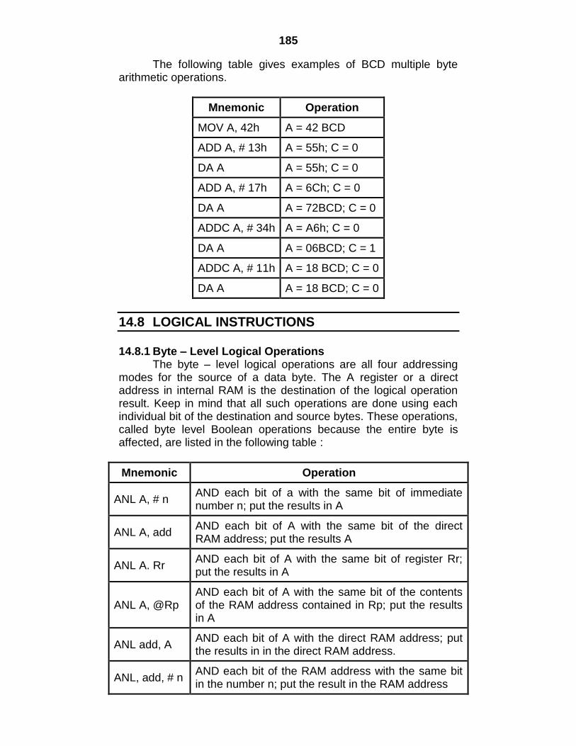
185
The following table gives examples of BCD multiple byte arithmetic operations.
Mnemonic Operation
MOV A, 42h A = 42 BCD
ADD A, # 13h A = 55h; C = 0
DA A A = 55h; C = 0
ADD A, # 17h A = 6Ch; C = 0
DA A A = 72BCD; C = 0
ADDC A, # 34h A = A6h; C = 0
DA A A = 06BCD; C = 1
ADDC A, # 11h A = 18 BCD; C = 0
DA A A = 18 BCD; C = 0
14.8 LOGICAL INSTRUCTIONS
14.8.1 Byte – Level Logical Operations The byte – level logical operations are all four addressing modes for the source of a data byte. The A register or a direct address in internal RAM is the destination of the logical operation result. Keep in mind that all such operations are done using each individual bit of the destination and source bytes. These operations, called byte level Boolean operations because the entire byte is affected, are listed in the following table :
Mnemonic Operation
ANL A, # n AND each bit of a with the same bit of immediate number n; put the results in A
ANL A, add AND each bit of A with the same bit of the direct RAM address; put the results A
ANL A. Rr AND each bit of A with the same bit of register Rr; put the results in A
ANL A, @Rp AND each bit of A with the same bit of the contents of the RAM address contained in Rp; put the results in A
ANL add, A AND each bit of A with the direct RAM address; put the results in in the direct RAM address.
ANL, add, # n AND each bit of the RAM address with the same bit in the number n; put the result in the RAM address
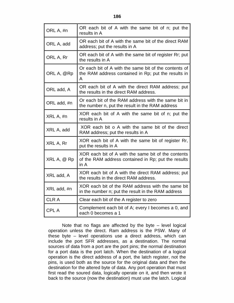
186
ORL A, #n OR each bit of A with the same bit of n; put the results in A
ORL A, add OR each bit of A with the same bit of the direct RAM address; put the results in A
ORL A, Rr OR each bit of A with the same bit of register Rr; put the results in A
ORL A, @Rp Or each bit of A with the same bit of the contents of the RAM address contained in Rp; put the results in A
ORL add, A OR each bit of A with the direct RAM address; put the results in the direct RAM address.
ORL add, #n Or each bit of the RAM address with the same bit in the number n, put the result in the RAM address
XRL A, #n XOR each bit of A with the same bit of n; put the results in A
XRL A, add XOR each bit o A with the same bit of the direct RAM address; put the results in A
XRL A, Rr XOR each bit of A with the same bit of register Rr, put the results in A
XRL A, @ Rp XOR each bit of A with the same bit of the contents of the RAM address contained in Rp; put the results in A
XRL add, A XOR each bit of A with the direct RAM address; put the results in the direct RAM address.
XRL add, #n XOR each bit of the RAM address with the same bit in the number n; put the result in the RAM address
CLR A Clear each bit of the A register to zero
CPL A Complement each bit of A; every I becomes a 0, and each 0 becomes a 1
Note that no flags are affected by the byte – level logical operation unless the direct. Ram address is the PSW. Many of these byte – level operations use a direct address, which can include the port SFR addresses, as a destination. The normal sources of data from a port are the port pins; the normal destination for a port data is the port latch. When the destination of a logical operation is the direct address of a port, the latch register, not the pins, is used both as the source for the original data and then the destination for the altered byte of data. Any port operation that must first read the soured data, logically operate on it, and then wrote it back to the source (now the destination) must use the latch. Logical
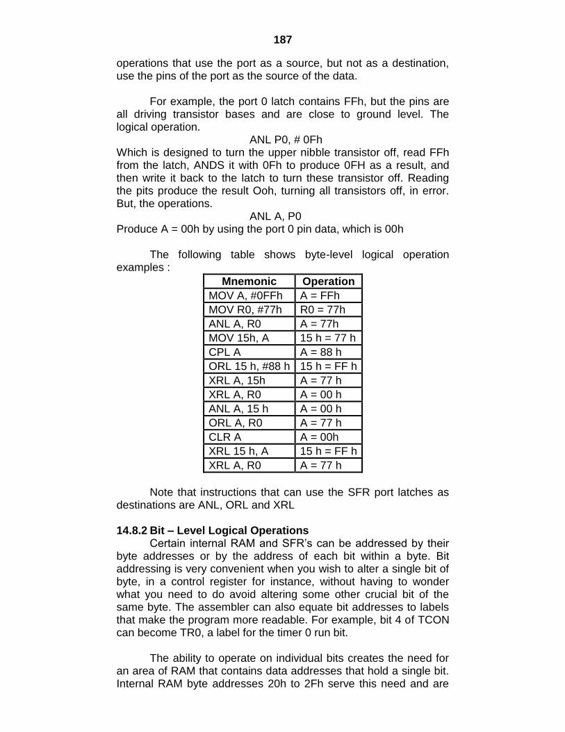
187
operations that use the port as a source, but not as a destination, use the pins of the port as the source of the data. For example, the port 0 latch contains FFh, but the pins are all driving transistor bases and are close to ground level. The logical operation. ANL P0, # 0Fh Which is designed to turn the upper nibble transistor off, read FFh from the latch, ANDS it with 0Fh to produce 0FH as a result, and then write it back to the latch to turn these transistor off. Reading the pits produce the result Ooh, turning all transistors off, in error. But, the operations. ANL A, P0 Produce A = 00h by using the port 0 pin data, which is 00h The following table shows byte-level logical operation examples :
Mnemonic Operation
MOV A, #0FFh A = FFh
MOV R0, #77h R0 = 77h
ANL A, R0 A = 77h
MOV 15h, A 15 h = 77 h
CPL A A = 88 h
ORL 15 h, #88 h 15 h = FF h
XRL A, 15h A = 77 h
XRL A, R0 A = 00 h
ANL A, 15 h A = 00 h
ORL A, R0 A = 77 h
CLR A A = 00h
XRL 15 h, A 15 h = FF h
XRL A, R0 A = 77 h
Note that instructions that can use the SFR port latches as
destinations are ANL, ORL and XRL 14.8.2 Bit – Level Logical Operations Certain internal RAM and SFR‟s can be addressed by their byte addresses or by the address of each bit within a byte. Bit addressing is very convenient when you wish to alter a single bit of byte, in a control register for instance, without having to wonder what you need to do avoid altering some other crucial bit of the same byte. The assembler can also equate bit addresses to labels that make the program more readable. For example, bit 4 of TCON can become TR0, a label for the timer 0 run bit. The ability to operate on individual bits creates the need for an area of RAM that contains data addresses that hold a single bit. Internal RAM byte addresses 20h to 2Fh serve this need and are
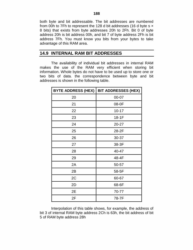
188
both byte and bit addressable. The bit addresses are numbered from 00h to 7Fh to represent the 128 d bit addresses (16 d byte s × 8 bits) that exists from byte addresses 20h to 2Fh. Bit 0 of byte address 20h is bit address 00h, and bit 7 of byte address 2Fh is bit address 7Fh. You must know you bits from your bytes to take advantage of this RAM area.
14.9 INTERNAL RAM BIT ADDRESSES
The availability of individual bit addresses in internal RAM makes the use of the RAM very efficient when storing bit information. Whole bytes do not have to be used up to store one or two bits of data. the correspondence between byte and bit addresses is shown in the following table.
BYTE ADDRESS (HEX) BIT ADDRESSES (HEX)
20 00-07
21 08-0F
22 10-17
23 18-1F
24 20-27
25 28-2F
26 30-37
27 38-3F
28 40-47
29 48-4F
2A 50-57
2B 58-5F
2C 60-67
2D 68-6F
2E 70-77
2F 78-7F
Interpolation of this table shows, for example, the address of bit 3 of internal RAM byte address 2Ch is 63h, the bit address of bit 5 of RAM byte address 28h
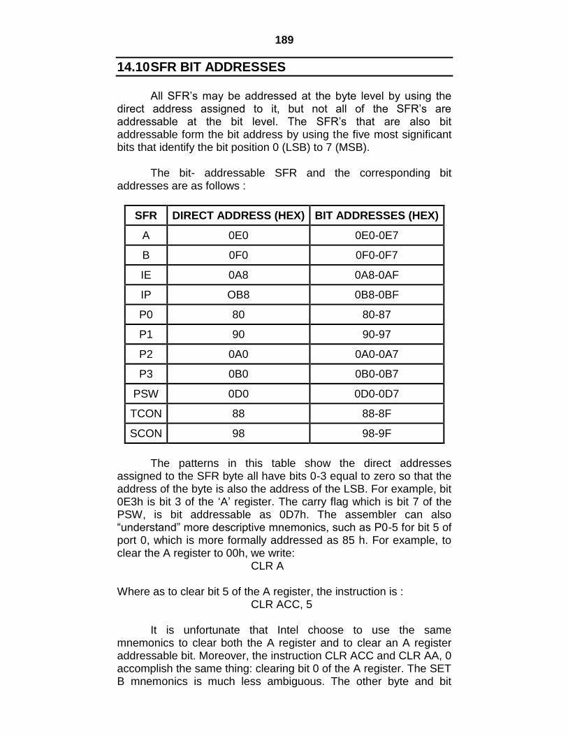
189
14.10 SFR BIT ADDRESSES
All SFR‟s may be addressed at the byte level by using the direct address assigned to it, but not all of the SFR‟s are addressable at the bit level. The SFR‟s that are also bit addressable form the bit address by using the five most significant bits that identify the bit position 0 (LSB) to 7 (MSB). The bit- addressable SFR and the corresponding bit addresses are as follows :
SFR DIRECT ADDRESS (HEX) BIT ADDRESSES (HEX)
A 0E0 0E0-0E7
B 0F0 0F0-0F7
IE 0A8 0A8-0AF
IP OB8 0B8-0BF
P0 80 80-87
P1 90 90-97
P2 0A0 0A0-0A7
P3 0B0 0B0-0B7
PSW 0D0 0D0-0D7
TCON 88 88-8F
SCON 98 98-9F
The patterns in this table show the direct addresses assigned to the SFR byte all have bits 0-3 equal to zero so that the address of the byte is also the address of the LSB. For example, bit 0E3h is bit 3 of the „A‟ register. The carry flag which is bit 7 of the PSW, is bit addressable as 0D7h. The assembler can also “understand” more descriptive mnemonics, such as P0-5 for bit 5 of port 0, which is more formally addressed as 85 h. For example, to clear the A register to 00h, we write: CLR A Where as to clear bit 5 of the A register, the instruction is : CLR ACC, 5 It is unfortunate that Intel choose to use the same mnemonics to clear both the A register and to clear an A register addressable bit. Moreover, the instruction CLR ACC and CLR AA, 0 accomplish the same thing: clearing bit 0 of the A register. The SET B mnemonics is much less ambiguous. The other byte and bit
190
mnemonic is CPL (complement) Figure 4 shows all the bit – addressable SFRs and the function of each addressable bit:
14.11 BIT – LEVEL BOOLEAN OPERATIONS
The bit – level Boolean logical opcodes operate on any addressable RAM or SFR bit. The carry flag in the PSW special – function register is the destination for most of the opcodes because the flag can be tested. The following table lists the Boolean bit level operations :
Mnemonic Operation
ANL C, b AND C and the addressed bit; put the result in C
ANL C, /b AND C and the complement of the addressed bit; put the result in C; the addressed bit is not altered
ORL C,b OR C and the addressed bit; put the result in C
ORL C, /b OR C and the complement of the addressed bit; put the result in C; the addressed bit is not altered
CPL C Complement the C flag
CPL b Complement the addressed bit
CLR C Clear the C flag to zero
CLR b Clear the addressed bit to zero
MOV C, b Copy the addressed bit to the C flag
MOV b, C Copy the C flag to the addressed bit
SETB C Set the flag to one
SETB b Set the addressed bit to one
Note that no flags, other than the C flag, are affected, unless the flag is an addressed bit. As is the case for byte-logical operations when addressing ports an destinations a port bit used a destination for a logical operation is part of the SFR latch, not the pin. A port bit used as a source only is a pin, not the latch. The bit instructions that can use a SFR latch bit are : CLR CPL, MOV and SET B.
191
Bit-level logical operation examples are shown in the following tables :
Mnemonic Operation
SETB 00h Bit 0 or RAM byte 20h = 1
MOV C, 00h C = 1
MOV 7Fh, C Bit 7 of RAM byte 2Fh = 1
ANL C,/00h C = 0; bit 0 of RAM byte 20h = 1
ORL C, 00h C = 1
CPL 7Fh Bit 7 of RAM byte 2Fh = 0
CLR C C = 0
ORL C,/7Fh C = 1; bit 7 of RAM byte 2Fh = 0
14.12 ROTATE AND SWAP OPERATIONS
The ability to rotate data is useful for inspecting bits of a byte without using individual bit opcodes. The A register can be rotated one bit position to the left for right with or without including the C flag in the rotation. If the C flag is not included, then the rotation involves the eight-bits of the A register. If the C flag is included, then nine bits are involved in the rotation. Including the C flag enables the programmer to construct rotate of as a rotate operations involving any number of bytes. The SWAP instruction can be thought of as a rotation of nibbles in the A register. Figure 5 diagrams the rotate and swap operations which are given in the following table :
Mnemonic Operation
RL A Rotate the A register one bit position to the left; bit A0 to bit A1, A1 to A2, A2 to A3, A3 to A4, A4 to A5, A5 to A6, A6 to A7 and A7 to A0
RLC A
Rotate the A register and the carry flag, as a ninth bit, one bit position to the left; bit A0 to bit A1, A1 to A2, A2 to A3, A3 to A4, A4 to A5, A5 to A6, A6 to A7, A7 to the carry flag and the carry flag to A0
RR A Rotate the A register one bit position to the right; bit A0 to bit A7, A6 to A5, A5 to A4, A4 to A3, A3 to A2, A2 to A1 and A1 to A0
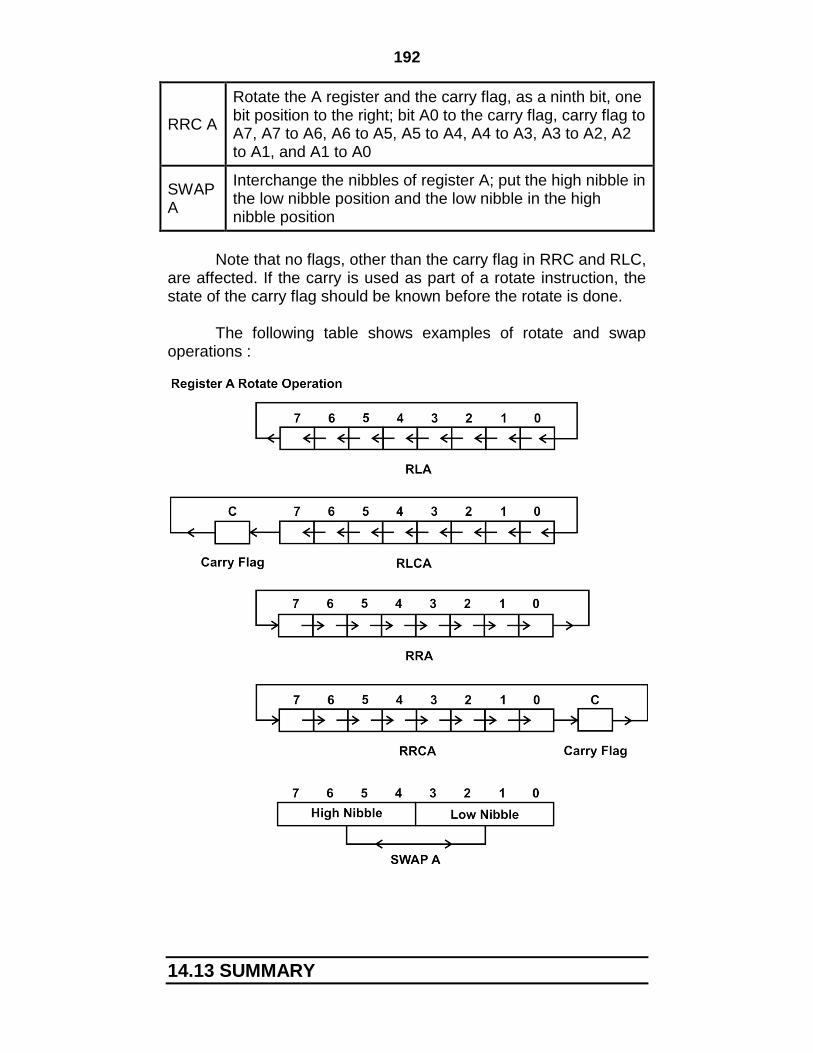
192
RRC A
Rotate the A register and the carry flag, as a ninth bit, one bit position to the right; bit A0 to the carry flag, carry flag to A7, A7 to A6, A6 to A5, A5 to A4, A4 to A3, A3 to A2, A2 to A1, and A1 to A0
SWAP A
Interchange the nibbles of register A; put the high nibble in the low nibble position and the low nibble in the high nibble position
Note that no flags, other than the carry flag in RRC and RLC,
are affected. If the carry is used as part of a rotate instruction, the state of the carry flag should be known before the rotate is done.
The following table shows examples of rotate and swap operations :
14.13 SUMMARY
193
Signed numbers use a 1 in bit position 7 of the MSB as a negative sign and a 0 as a positive sign.
The OV flag also signals that the sum exceeds the largest positive or negative numbers thought to be needed in the program.
Multiplication and division treat the numbers in registers A and B as unsigned.
Certain internal RAM and SFR‟s can be addressed by their byte addresses or by the address of each bit within a byte.
All SFR‟s may be addressed at the byte level by using the direct address assigned to it, but not all of the SFR‟s are addressable at the bit level.
The A register can be rotated one bit position to the left for right with or without including the C flag in the rotation.
14.14 REVIEW QUESTIONS
Q.1 Explain the different flags in 8051 Q.2 Explain ADD instruction with suitable example. Q.3 Explain SUB instruction with suitable example. Q.4 Explain MUL instruction. Q.5 Explain DIV instruction. Q.6 Explain different Rotate instruction.
14.15 REFERENCE
The 8051 Microcontroller by Kenneth J. Ayala, Publisher:
Thomson Delmar Learning The 8051 Microcontroller And Embedded Systems Using
Assembly And C, 2/E By Mazidi and Mazidi, Publisher: Pearson Education India
194
15
JUMP, CALL AND SUBROUTINES
15.1 Introduction
15.2 The Jump and Call Program Range
15.3 Relative Range
15.4 Jumps
15.5 Calls and Subroutines
15.6 Interrupts and Returns
15.7 Summary
15.8 Review Questions
15.9 Reference After studying this chapter you should be able to Describe the jump and call program range of the 8051
microcontroller. Study different types of jump instructions. Understand the call instructions and subroutines Study different types of return instructions.
15.1 INTRODUCTION
The jumps and calls discussed in this chapter are decision codes that alter the flow of the program by examining the results of the action codes and changing the contents of the program counter. A jump permanently changes the contents of the program counter if certain program conditions exist. A call temporarily changes the program counter to allow another part of the program to run. Jumps and calls may also be generically referred to as “branches”, which emphasizes that two divergent paths are made possible by this type of instruction.
15.2 THE JUMP AND CALL PROGRAM RANGE
A jump or call instruction can replace the contents of the
program counter with a new program address number that causes program execution to begin at the code located at the new address. The difference, in bytes, of this new address from the address in
195
the program where the jump or call is located is called the range of the jump or call. For example, if a jump instruction is located at program address 0100h, and the jump causes the program counter to become 0120h, then the range of the jump is 20h bytes.
Jump or call instructions may have one of three ranges: a relative range of +127d, -128d bytes from the instruction following the jump or call instruction; an absolute range on the same 2K byte page as the instruction following the jump or call; or along range of any address from 0000h to FFFFh, anywhere in program memory. Figure 1 shows the relative range of all the jump instructions. FIGURE 1: Jump Instruction Ranges
196
15.3 RELATIVE RANGE
Jump that replaces the PC (program counter) content with a new address that is greater than (the address following the jump instruction by 127 or less) or less than (the address following the jump by 128 or less) is called a relative jump. Schematically, the relative jump can be shown as follows: -
They are so named because the address that is placed in program counter is relative to the address where the jump occurs. If the absolute address of the jump instruction changes, then the jump address changes also but remains the same distance away from the jump away from the jump instruction. The address following the jump is used to calculate the relative jump because of the action of the PC. The PC is incremented to point to the next instruction before the current instruction is executed. Thus, the PC is set to the following address before the jump instruction is executed, or in the vernacular: “before the jump is taken.” Relative jumping has two advantages: 1] Only one byte of data need be specified, either in positive format for jumps ahead in the program or in 2‟s complement negative format for jumps behind. The jump address displacement byte can then be added to the PC to get the absolute address. Specifying only one byte saves program bytes & speeds up program execution. 2] The program that is written using relative jumps can be located anywhere in the program address space without re-assembling the code to generate absolute addresses. The disadvantage of using relative addressing is the requirement that all addresses jumped be within a range of +127d, -128d bytes of the jump instruction. This range is not a serious
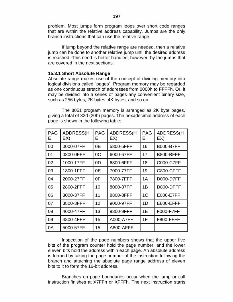
197
problem. Most jumps form program loops over short code ranges that are within the relative address capability. Jumps are the only branch instructions that can use the relative range. If jump beyond the relative range are needed, then a relative jump can be done to another relative jump until the desired address is reached. This need is better handled, however, by the jumps that are covered in the next sections. 15.3.1 Short Absolute Range Absolute range makes use of the concept of dividing memory into logical divisions called “pages”. Program memory may be regarded as one continuous stretch of addresses from 0000h to FFFFh. Or, it may be divided into a series of pages any convenient binary size, such as 256 bytes, 2K bytes, 4K bytes, and so on. The 8051 program memory is arranged as 2K byte pages, giving a total of 32d (20h) pages. The hexadecimal address of each page is shown in the following table:
PAGE
ADDRESS(HEX)
PAGE
ADDRESS(HEX)
PAGE
ADDRESS(HEX)
00 0000-07FF 0B 5800-5FFF 16 B000-B7FF
01 0800-0FFF 0C 6000-67FF 17 B800-BFFF
02 1000-17FF 0D 6800-6FFF 18 C000-C7FF
03 1800-1FFF 0E 7000-77FF 19 C800-CFFF
04 2000-27FF 0F 7800-7FFF 1A D000-D7FF
05 2800-2FFF 10 8000-87FF 1B D800-DFFF
06 3000-37FF 11 8800-8FFF 1C E000-E7FF
07 3800-3FFF 12 9000-97FF 1D E800-EFFF
08 4000-47FF 13 9800-9FFF 1E F000-F7FF
09 4800-4FFF 15 A000-A7FF 1F F800-FFFF
0A 5000-57FF 15 A800-AFFF
Inspection of the page numbers shows that the upper five bits of the program counter hold the page number, and the lower eleven bits hold the address within each page. An absolute address is formed by taking the page number of the instruction following the branch and attaching the absolute page range address of eleven bits to it to form the 16-bit address. Branches on page boundaries occur when the jump or call instruction finishes at X7FFh or XFFFh. The next instruction starts
198
at X800h or X000h, which places the jump or call address on the same page as the next instruction after the jump or call. The page change presents no problem when branching ahead but could be troublesome if the branch is backwards in the program. The assembler should flag such programs as errors, so adjustments can be made by the programmer to use a different type of range. Absolute range addressing has the same advantages as relative addressing; fewer bytes are needed and the code is relocatable as long as the relocated code begins at the start of a page. Absolute addressing has the advantage of allowing jumps or calls over longer programming distances than does relative addressing. 15.3.2 Long Absolute Range
Addresses that can access the entire program space from 0000h to FFFFh use long range addressing. Long range addresses require more bytes of code to specify and are relocatable only at the beginning of 64K byte pages. Since we are limited to a nominal ROM address range of 64K bytes, the program must be re-assembled every time a long range address changes and these branches are not generally relocatable.
Long range addressing has the advantage of advantage of using the entire program address space available to the 8051. It is most likely to be used in large programs.
15.4 JUMPS
The ability of a program to respond quickly to changes in conditions depends largely upon the number and types of jump instructions available to the programmer. The 8051 has a rich set of jumps that can operate at the bit and byte levels. These jump opcodes are one reason the 8051 is such a powerful microcontroller. Jumps operate by testing for conditions that are specified in the jump mnemonic. If the condition is true, then the jump is taken – that is, the program counter is altered to the address that is part of the jump instruction. If the condition is false, then the instruction immediately following the jump instruction is executed because the program counter is not altered. Keep in mind that the conditions of true dose not mean a binary 1 and that false does not mean binary 0. The condition specified by the mnemonic is either true or false. 15.4.1 Bit Jumps
199
Bit jumps all operate according to the status of the carry flag in the PSW or the status of any bit-addressable location. All bit jumps are relative to the program counter. Jump instructions that test for bit conditions are shown in the following table: Mnemonic Operation JC radd Jump relative if the carry flag is set to 1 JNC radd Jump relative if the carry flag is reset to 0 JB b,radd Jump relative if addressable bit is set to 1 JNB b,radd Jump relative if addressable bit is reset to 0 JBC b,radd Jump relative if addressable bit is set, and
clear the addressable bit to 0 Note that no flags are affected unless the bit in JBC is a flag bit in the PSW. When the bit used in a JBC instruction is a port bit, the SFR latch for that port is read, tested, and altered. 15.4.2 Byte Jumps Byte jumps – jump instructions that test bytes of data – behave as bit jumps. If the condition that is tested is true, the jump is taken; if the condition is false, the instruction after the jump is executed. All byte jumps are relative to the program counter. The following table lists examples of byte jumps: Mnemonics Operation CJNE A,add,radd Compare the contents of the A register
with the contents of the Direct address; if they are not equal , then jump to the relative address; set the carry flag to 1 if A is less than the contents of the direct address; otherwise, set the carry flag to 0
CJNE A,#n,radd Compare the content of the A resistor with the immediate number n; if they are not equal, then jump to the relative address; set the carry flag to 1 if A is less than the number; otherwise, set the carry flag to 0
CJNE Rn,#n,radd Compare the contents of register Rn with the immediate number n; if they are not equal, then jump to the relative address; set the carry flag to 1 if Rn is less than the number; otherwise, set the carry flag to 0
200
CJNE @Rp,#n,radd Compare the contents of the address contained in register Rp to the number n; if they are not equal, then jump to the relative address; set the carry flag to 1 if the contents of the address in Rp are less than the number; otherwise, set the carry flag to 0
DJNZ Rn,radd Decrement register Rn by 1 and jump to the relative address if the result is not zero; no flags are affected
DJNZ add,radd Decrement the direct address by 1 and jump to the relative address if the result is not 0; the flags are affected unless the direct address is the PSW
JZ radd Jump to the relative address if A is 0; the flags and the A register are not changed
JNZ radd Jump to the relative address if A is not 0; the flags and the A register are not changed
Note that if the direct address used in a DJNZ is a port, the port
SFR is decremented and tested for 0 15.4.3 Unconditional Jumps Unconditional jumps do not test any bit or byte to determine whether the jump should be taken. The jump is always taken. All jump ranges are found in this group of jumps, and these are the only jumps that can jump to any location in memory.
The following table shows examples of unconditional jumps: Mnemonics Operation JMP @A+ DPTR Jump to the address formed by adding A to
the DPTR; this is an unconditional jump and will always be done; the address can be anywhere in program memory; A, the DPTR, and the flags are unchanged.
AJMP sadd Jump to absolute short range address sad; this is an unconditional jump and is always taken; no flags are affected
LJMP ladd Jump to absolute long range address ladd; this is an unconditional
Jump and is always taken; no flags are affected
SJMP radd Jump to relative address radd; this is an unconditional jump and is always taken; no flags are affected.
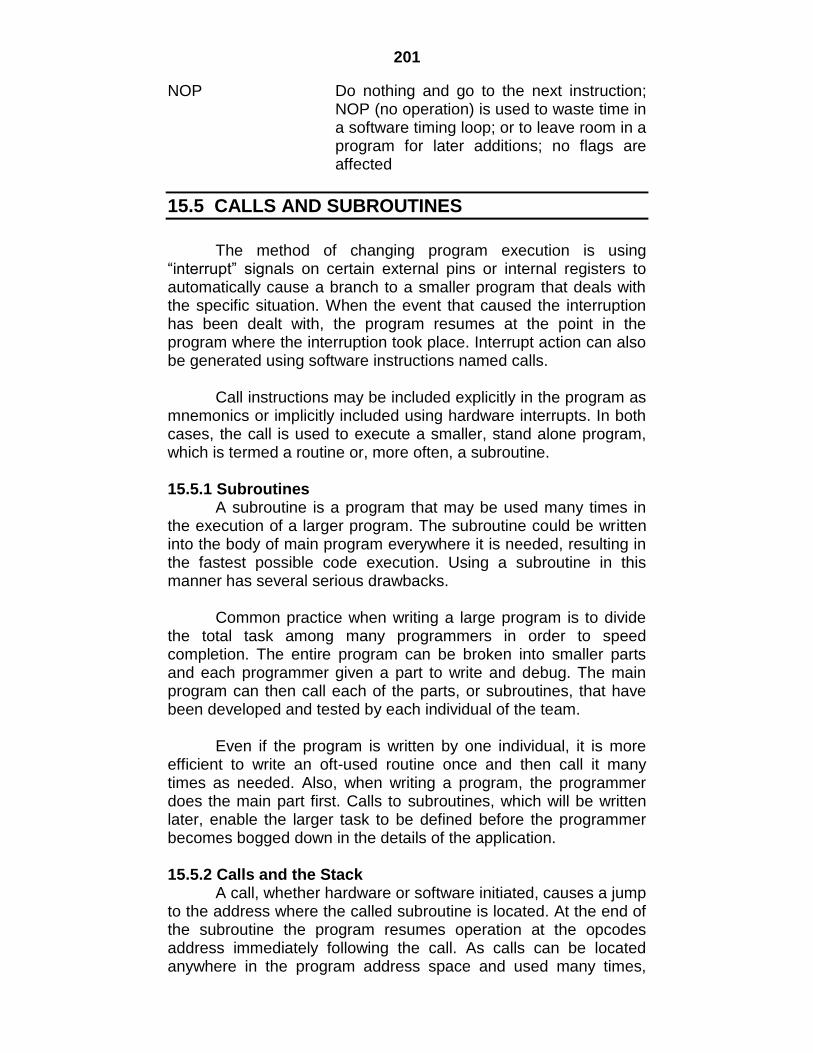
201
NOP Do nothing and go to the next instruction; NOP (no operation) is used to waste time in a software timing loop; or to leave room in a program for later additions; no flags are affected
15.5 CALLS AND SUBROUTINES
The method of changing program execution is using “interrupt” signals on certain external pins or internal registers to automatically cause a branch to a smaller program that deals with the specific situation. When the event that caused the interruption has been dealt with, the program resumes at the point in the program where the interruption took place. Interrupt action can also be generated using software instructions named calls. Call instructions may be included explicitly in the program as mnemonics or implicitly included using hardware interrupts. In both cases, the call is used to execute a smaller, stand alone program, which is termed a routine or, more often, a subroutine. 15.5.1 Subroutines A subroutine is a program that may be used many times in the execution of a larger program. The subroutine could be written into the body of main program everywhere it is needed, resulting in the fastest possible code execution. Using a subroutine in this manner has several serious drawbacks. Common practice when writing a large program is to divide the total task among many programmers in order to speed completion. The entire program can be broken into smaller parts and each programmer given a part to write and debug. The main program can then call each of the parts, or subroutines, that have been developed and tested by each individual of the team. Even if the program is written by one individual, it is more efficient to write an oft-used routine once and then call it many times as needed. Also, when writing a program, the programmer does the main part first. Calls to subroutines, which will be written later, enable the larger task to be defined before the programmer becomes bogged down in the details of the application. 15.5.2 Calls and the Stack A call, whether hardware or software initiated, causes a jump to the address where the called subroutine is located. At the end of the subroutine the program resumes operation at the opcodes address immediately following the call. As calls can be located anywhere in the program address space and used many times,
202
there must be an automatic means of storing the address of the instruction following the call so that program execution can continue after the subroutine has executed. The stack area of internal RAM is used to automatically store the address, called the return address, of the instruction found immediately after the call. The stack pointer register holds the address of the last space used on the stack. It stores the return address above this place, adjusting itself upward as return address is stored. The term “stack” and “stack pointer” are often used interchangeably to designate the top of the stack area in RAM that is pointed to by the stack pointer.
Figure 2 diagram the following sequence of events:
1. A call opcodes occurs in the program software, or an interrupt is generated in the hardware circuitry.
2. The return address of the next instruction after the call instruction or interrupt is found in the program counter.
3. The return address bytes are pushed on the stack, low byte first.
4. The stack pointer is incremented for each push on the stack.
5. The subroutine address is placed in the program counter.
6. The subroutine address is executed.
7. A RET (return) opcode is encountered at the end of the subroutine.
FIGURE 2 Storing and Retrieving the Return Address.
8. Two pop operations restore the return address to the PC from
the stack area in internal RAM. 9. The stack pointer is decremented for each address byte pop. All of these steps are automatically handled by the 8051
hardware. It is the responsibility of the programmer to ensure that the subroutine ends in a RET instruction and that the stack does not grow up into data areas that are used by the program.
203
15.5.3 Calls and Returns Calls use short or long range addressing: returns have no addressing mode specified but are always long range. The following table shows examples of call opcodes: Mnemonic Operation ACALL sadd Call the subroutine located on the same
page as the address of the opcodes immediately following the ACALL instruction; push the address of the instruction immediately after the call on the stack
LCALL ladd Call the subroutine located anywhere in program memory space; push the address of the instruction immediately following the call on the stack
RET Pop two bytes from the stack into the program counter
Note that no flags are affected unless the stack pointer has been allowed to erroneously reach the address of the PSW special function register.
15.6 INTERRUPTS AND RETURNS
An interrupt is a hardware-generated call. Just as a call opcodes can be located within a program to automatically access a subroutine, certain pins on the 8051 can cause a call when external electrical signals on them go to a low state. Internal operations of the timers and the serial port can also cause an interrupt call to take place. The subroutines called by an interrupt are located at fixed hardware addresses. The following table shows the interrupt subroutine addresses. INTERRUPT ADDRESS (HEX) CALLED IE0 0003 TF0 000B IE1 0013 TF1 001B SERIAL 0023 When an interrupt call takes place, hardware interrupt disable flip-flops are set to prevent another interrupt of the same priority level from taking place until an interrupt return instruction has been executed in the interrupt subroutine. The action of the interrupt routine is shown in table below.
204
Mnemonic Operation RETI Pop two bytes from the stack into the
program counter and reset the interrupt enable flip-flops
Note that the only difference between the RET and RETI instructions is the enabling of the interrupt logic when RETI is used. RET is used at the ends of subroutines called by an opcodes. RETI is used by subroutines called by an interrupt. The following program examples use a call to a subroutine. ADDRESS MNEMONIC COMMENT MAIN: MOV 81h, #30h ; set the stack pointer to 30h in RAM LCALL SUB ; push address of NOP; PC = #SUB; SP = 32h NOP ;return from SUB to this opcodes . . . . . . SUB MOV A, #45h ;SU loads A with 45h and returns RET ;pop return address to PC; SP = 30h In the following example of an interrupt call to a routine, timer 0 is used in mode 0 to overflow and set the timer 0 interrupt flag. When the interrupt is generated, the program vector to the interrupt routine, resets the timer 0 interrupt flag, stop the timer, and returns. ADDRESS MNEMONIC COMMENT .0RG 0000h ;begin program at 0000 AJMP OVER ;jump over interrupt subroutine .0RG 000Bh ;put timer 0 interrupt subroutine here CLR 8Ch ;stop timer 0; set TRO = 0 RETI ;return and enable interrupt structure OVER: MOV 0A8h, #82h ; enable the timer 0 interrupt in the IE MOV 89h, #00h ;set timer operation, mode 0 MOV 8Ah, #00h ;clear TL0 MOV 8Ch, #00h ;clearTH0 SET 8Ch ;start timer 0; set TR0 = 1
205
; ; ; ; the program will continue on and be interrupted when the timer has timed out
15.7 SUMMARY
Jump alter program flow by replacing the PC counter
contents with the address of the jump address. Jumps have the following ranges:
Relative : up to PC +127 bytes, PC – 128 bytes away from PC Absolute short : anywhere on a 2K-byte page Absolute long : anywhere in program memory
Jump opcodes can test an individual bit, or a byte, to check for conditions that make the program jump to a new program address.
Bit jumps all operate according to the status of the carry flag
in the PSW or the status of any bit-addressable location.
Unconditional jumps do not test any bit or byte to determine whether the jump should be taken. The jump is always taken. All jump ranges are found in this group of jumps, and these are the only jumps that can jump to any location in memory.
15.8 REVIEW QUESTIONS
Q.1 Explain the relative range. Q.2 What do you mean by absolute short range and long range? Q.3 Explain bit and byte jump instructions. Q.4 Explain subroutine program. Q.5 Explain different return instructions.
15.9 REFERENCE
The 8051 Microcontroller by Kenneth J. Ayala, Publisher:
Thomson Delmar Learning The 8051 Microcontroller And Embedded Systems Using
Assembly And C, 2/E By Mazidi and Mazidi, Publisher: Pearson Education India
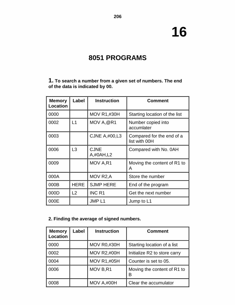
206
16
8051 PROGRAMS
1. To search a number from a given set of numbers. The end
of the data is indicated by 00.
Memory Location
Label Instruction Comment
0000 MOV R1,#30H Starting location of the list
0002 L1 MOV A,@R1 Number copied into accumlater
0003 CJNE A,#00,L3 Compared for the end of a list with 00H
0006 L3 CJNE A,#0AH,L2
Compared with No. 0AH
0009 MOV A,R1 Moving the content of R1 to A
000A MOV R2,A Store the number
000B HERE SJMP HERE End of the program
000D L2 INC R1 Get the next number
000E JMP L1 Jump to L1
2. Finding the average of signed numbers.
Memory Location
Label Instruction Comment
0000 MOV R0,#30H Starting location of a list
0002 MOV R2,#00H Initialize R2 to store carry
0004 MOV R1,#05H Counter is set to 05.
0006 MOV B,R1 Moving the content of R1 to B
0008 MOV A,#00H Clear the accumulator
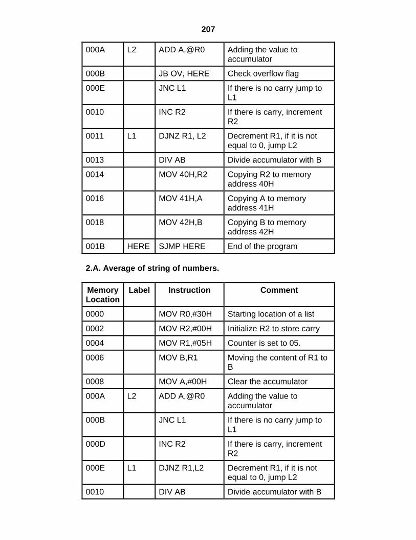
207
000A L2 ADD A,@R0 Adding the value to accumulator
000B JB OV, HERE Check overflow flag
000E JNC L1 If there is no carry jump to L1
0010 INC R2 If there is carry, increment R2
0011 L1 DJNZ R1, L2 Decrement R1, if it is not equal to 0, jump L2
0013 DIV AB Divide accumulator with B
0014 MOV 40H,R2 Copying R2 to memory address 40H
0016 MOV 41H,A Copying A to memory address 41H
0018 MOV 42H,B Copying B to memory address 42H
001B HERE SJMP HERE End of the program
2.A. Average of string of numbers.
Memory Location
Label Instruction Comment
0000 MOV R0,#30H Starting location of a list
0002 MOV R2,#00H Initialize R2 to store carry
0004 MOV R1,#05H Counter is set to 05.
0006 MOV B,R1 Moving the content of R1 to B
0008 MOV A,#00H Clear the accumulator
000A L2 ADD A,@R0 Adding the value to accumulator
000B JNC L1 If there is no carry jump to L1
000D INC R2 If there is carry, increment R2
000E L1 DJNZ R1,L2 Decrement R1, if it is not equal to 0, jump L2
0010 DIV AB Divide accumulator with B
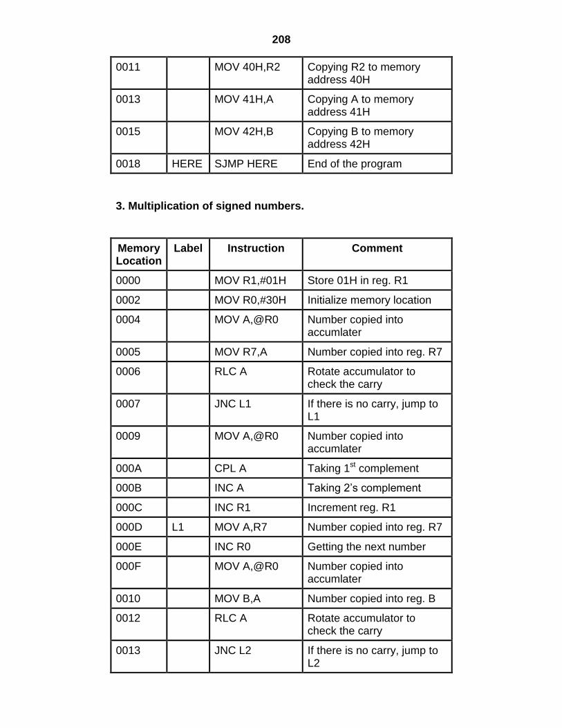
208
0011 MOV 40H,R2 Copying R2 to memory address 40H
0013 MOV 41H,A Copying A to memory address 41H
0015 MOV 42H,B Copying B to memory address 42H
0018 HERE SJMP HERE End of the program
3. Multiplication of signed numbers.
Memory Location
Label Instruction Comment
0000 MOV R1,#01H Store 01H in reg. R1
0002 MOV R0,#30H Initialize memory location
0004 MOV A,@R0 Number copied into accumlater
0005 MOV R7,A Number copied into reg. R7
0006 RLC A Rotate accumulator to check the carry
0007 JNC L1 If there is no carry, jump to L1
0009 MOV A,@R0 Number copied into accumlater
000A CPL A Taking 1st complement
000B INC A Taking 2‟s complement
000C INC R1 Increment reg. R1
000D L1 MOV A,R7 Number copied into reg. R7
000E INC R0 Getting the next number
000F MOV A,@R0 Number copied into accumlater
0010 MOV B,A Number copied into reg. B
0012 RLC A Rotate accumulator to check the carry
0013 JNC L2 If there is no carry, jump to L2
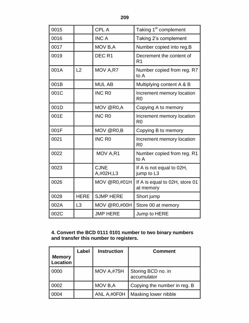
209
0015 CPL A Taking 1st complement
0016 INC A Taking 2‟s complement
0017 MOV B,A Number copied into reg.B
0019 DEC R1 Decrement the content of R1
001A L2 MOV A,R7 Number copied from reg. R7 to A
001B MUL AB Multiplying content A & B
001C INC R0 Increment memory location R0
001D MOV @R0,A Copying A to memory
001E INC R0 Increment memory location R0
001F MOV @R0,B Copying B to memory
0021 INC R0 Increment memory location R0
0022 MOV A,R1 Number copied from reg. R1 to A
0023 CJNE A,#02H,L3
If A is not equal to 02H, jump to L3
0026 MOV @R0,#01H If A is equal to 02H, store 01 at memory
0028 HERE SJMP HERE Short jump
002A L3 MOV @R0,#00H Store 00 at memory
002C JMP HERE Jump to HERE
4. Convert the BCD 0111 0101 number to two binary numbers and transfer this number to registers.
Memory Location
Label Instruction Comment
0000 MOV A,#75H Storing BCD no. in accumulator
0002 MOV B,A Copying the number in reg. B
0004 ANL A,#0F0H Masking lower nibble
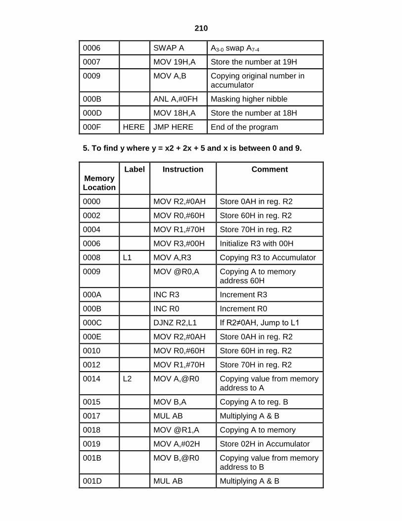
210
0006 SWAP A A3-0 swap A7-4
0007 MOV 19H,A Store the number at 19H
0009 MOV A,B Copying original number in accumulator
000B ANL A,#0FH Masking higher nibble
000D MOV 18H,A Store the number at 18H
000F HERE JMP HERE End of the program
5. To find y where y = x2 + 2x + 5 and x is between 0 and 9.
Memory Location
Label Instruction Comment
0000 MOV R2,#0AH Store 0AH in reg. R2
0002 MOV R0,#60H Store 60H in reg. R2
0004 MOV R1,#70H Store 70H in reg. R2
0006 MOV R3,#00H Initialize R3 with 00H
0008 L1 MOV A,R3 Copying R3 to Accumulator
0009 MOV @R0,A Copying A to memory address 60H
000A INC R3 Increment R3
000B INC R0 Increment R0
000C DJNZ R2,L1 If R2≠0AH, Jump to L1
000E MOV R2,#0AH Store 0AH in reg. R2
0010 MOV R0,#60H Store 60H in reg. R2
0012 MOV R1,#70H Store 70H in reg. R2
0014 L2 MOV A,@R0 Copying value from memory address to A
0015 MOV B,A Copying A to reg. B
0017 MUL AB Multiplying A & B
0018 MOV @R1,A Copying A to memory
0019 MOV A,#02H Store 02H in Accumulator
001B MOV B,@R0 Copying value from memory address to B
001D MUL AB Multiplying A & B
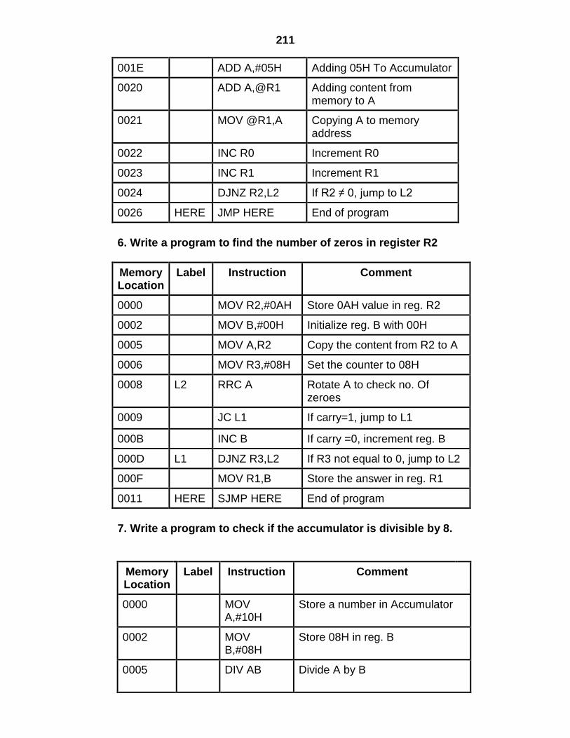
211
001E ADD A,#05H Adding 05H To Accumulator
0020 ADD A,@R1 Adding content from memory to A
0021 MOV @R1,A Copying A to memory address
0022 INC R0 Increment R0
0023 INC R1 Increment R1
0024 DJNZ R2,L2 If R2 ≠ 0, jump to L2
0026 HERE JMP HERE End of program
6. Write a program to find the number of zeros in register R2
Memory Location
Label Instruction Comment
0000 MOV R2,#0AH Store 0AH value in reg. R2
0002 MOV B,#00H Initialize reg. B with 00H
0005 MOV A,R2 Copy the content from R2 to A
0006 MOV R3,#08H Set the counter to 08H
0008 L2 RRC A Rotate A to check no. Of zeroes
0009 JC L1 If carry=1, jump to L1
000B INC B If carry =0, increment reg. B
000D L1 DJNZ R3,L2 If R3 not equal to 0, jump to L2
000F MOV R1,B Store the answer in reg. R1
0011 HERE SJMP HERE End of program
7. Write a program to check if the accumulator is divisible by 8.
Memory Location
Label Instruction Comment
0000 MOV A,#10H
Store a number in Accumulator
0002 MOV B,#08H
Store 08H in reg. B
0005 DIV AB
Divide A by B
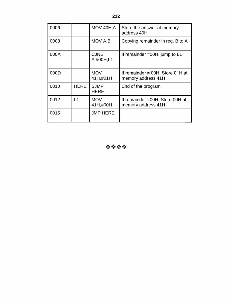
212
0006 MOV 40H,A
Store the answer at memory address 40H
0008 MOV A,B
Copying remainder in reg. B to A
000A CJNE A,#00H,L1
If remainder =00H, jump to L1
000D MOV 41H,#01H
If remainder ≠ 00H, Store 01H at memory address 41H
0010 HERE SJMP HERE
End of the program
0012 L1 MOV 41H,#00H
If remainder =00H, Store 00H at memory address 41H
0015 JMP HERE
213
Syllabus
F.Y.B.Sc. (IT), Sem - II,
Microprocessor & Microcontrollers
Unit I : Internet and WWW
What is Internet? Introduction to Internet and its applications, E-mail,
telnet, FTP, e-commerce, video conferencing, e-business. Internet
service providers, domain name server, internet address
World Wide Web (WWW)
World Wide Web and its evolution, uniform resource locator (URL),
browsers – internet explorer, netscape navigator, opera, firefox, chrome,
mozilla, search engine, web saver-apache, IIS, proxy server, HTTP
protocol
Unit II : HTML and Graphics
HTML Tag Reference, global Attributes, Event Handlers, Document
Structure Tags, Formatting Tags, text Level formatting, Block Level
formatting, List Tags, Hyperlink tags, Images and Image maps, Table
tags, Form Tags, Frame Tags, Executable content tags
Imagemaps
What are Imagemaps? Client-side Imagemaps, Server-side Imagemaps,
Using Server-slide and Client-side Imagemaps together, Alternative text
for Imagemaps,
Tables
Introduction to HTML tables and theirstructure, The table tags, Alignment,
Aligning Entire Table, Alignment within a row, Alignment within a cell,
Attributes, Content Summary, Background Color, Adding a Caption,
Setting the width, Adding a border, Spacing within a cell, Spacing
214
between the cells, Spanning multiple rows or columns, Elements that can
be placed in a table, Table Sections and column properties, Tables as a
design tool.
Frames
Introduction to Frames, Applications, Frames document, The
<FRAMESET> tag, Nesting <FRAMESET> tag, Placing content in frames
with the <FRAME> tag, Targeting named frames, Creating floating
frames, Using Hidden frames,
Forms
Creating Forms, The <FORM> tag, Named Input fields, The <INPUT>
tag, Multiple lines text windows, Drop down and list boxes, Hidden, Text,
Test Area, Password, File Upload, Button, Submit, Reset, radio,
Checkbox. Select, Option, Forms and Scripling, Action Buttons, Labelling
input files, Grouping related fields, Disabled and read-only fields, Form
field event handlers, Passing form data.
Style Sheets
What are style sheets? Why are style sheets valuable? Different
approaches to style sheets, Using Multiple approaches, Linking to style
information in s separate file, Setting up style information, Using the
<LINK> tag, Embedded style information, Using <STYLE> tag, Inline style
information.
Unit III : Java Script
Introduction, Client-Side JavaScript, Server-Side Java Script, Java Script
Objects, Java Script Security.
Operators
Assignment, Operators, Comparison Operators, Arithmetic Operators, %
(Modulus), ++ (Increment), -- (Decreemnt), - (Unary Negation), Logical
Operators, Short-Circuit Evaluation, String Operators, Special Operators,
: (Conditional operator), (Comma operator), delete, new, this, void
215
Statements
Break, comment, continue, delete, do…while, export, for, for….in,
function, if….else, import, labeled, return, switch, var, while, with,
Core JavaScript (Properties and Methods of Each)
Array, Boolean, Date, Function, Math, Number. Object, String, resExp
Document and its associated objects
Document, Link, Area, Anchor, Image. Applet, Layer
Events and Event Handlers
General Information about Events, Defining Even Handlers, event,
onAbort, onBlur, onChange, onClick, onDblClick, ondragDrop, onError,
onFocus, onKeyDown, onKeyPress, onKeyUp. onLoad, onMouseDown,
onMouseMove, onMouseOut, onMouseOver, onMouseUp, onMove,
onReset, onResize, onSelect, onSubmit, onUnload
Unit IV : XML
Introduction to XML, Anatomy of an XML document, Creating XML
Documents, Creating XML DTDs, XML Schemas, XSL.
Unit V : PHP
Why PHP and MySQL?, Server-side web scripting, Installing PHP,
Adding PHP to HTML, Syntax and Variables, Passing information
between pages, Strings, Arrays and Array Functions, Numbers, Basic
PHP errors/problems.
Unit VI : Advanced PHP and MySQL
PHP/MySQL Functions, Displaying queries in tables, Building Forms from
queries, String and Regular Expressions, Sessions, Cookies and HTTP,
Type and Type Conversions, E-Mail
216
Term Work and tutorial
Should contain minimum 5 assignments and two class tests
Practical : Should contain minimum 8 experiments
List of Practicals :
1. Design a web page using different text formatting tags
2. Design a web page with links to different pages and allow
navigation between pages.
3. Design a web page with Imagemaps
4. Design a web page with different tables. Design a webpage suing
table so that the content appeared well placed.
5. Design a web page using frames.
6. Design a web page with a form that uses all types of controls.
7. Design a website using style sheets so that the pages have uniform
style.
8. Using Java Script design a web page that prints factorial / Fibonacci
series / any given series.
9. Design a form with a test box and a command button. Using Java
script write a program whether the number entered in the text box is
a prime number or not.
10. Design a form and validate all the controls placed on the form using
Java Script.
11. Design a DTD, corresponding XML document and display it in
browser using CSS.
12. Design an XML document and display it in browser using XSL.
13. Design XML Schema and corresponding XML document.
14. Design a php page to process a form.
15. Design a php page for authenticating a user.
16. Design a complete dynamic website with all validations.