Embed Size (px)
Citation preview
Journal of Theoretical and Applied Information Technology 31
st October 2014. Vol. 68 No.3
© 2005 - 2014 JATIT & LLS. All rights reserved.
ISSN: 1992-8645 www.jatit.org E-ISSN: 1817-3195
630
DC- DC BOOST CONVERTER FOR SOLAR POWER
APPLICATION
1 P.MUTHUKRISHNAN,
2 R.DHANASEKARAN
1 Research Scholar, St.Peter’s University Chennai, TN, INDIA. 2 Professor & Director-Research, Syed Ammal Engineering College,
Ramanathapuram, TN, INDIA. E-mail: [email protected], 2 [email protected]
ABSTRACT
A Conventional Boost Converter is not capable for obtain a high voltage gain even extreme duty cycle maintain the triggering circuit diagram. In order to increase the voltage gain for the new Boost converter from the solar power application. In this paper boost converter specialty is achieved 10 times that of input voltage and more than 10 times of input voltages is possible from output side by using coupled inductor and parallel capacitor. The proposed boost converter output voltage is obtained 600V from source input of 60V and output power is 900 watts. The output voltage is high and voltage stress across the active switch is minimized and output ripples also minimized. In this paper the high power rating from low input voltage rating of the input source and also capable to go for AC power application whenever adding the inverter circuit to the main circuit diagram.
Keywords – Boost Converter, Coupled Inductor, Parallel Capacitor, High Voltage Gain, Soft
Switching.
1. INTRODUCTION
In Recent Years, wide use of electrical
equipment has forced strict demands for electrical utilizing energy and this development is constantly growing. Accordingly, researchers and governments worldwide have prepared on renewable energy applications for explanatory natural energy consumption and environmental location. Among different renewable energy sources, the photovoltaic cell and fuel cell have been considering attractive choice. However, without additional arrangements, the output voltages generated from both sources. Thus, a high step-up dc-dc converter is desired in the power conversion systems corresponding to these two energy sources. In addition to the mentioned applications, a high step-up dc-dc converter is also required by many industrial applications, such as high-intensity discharge lamp ballasts for automobile headlamps and battery backup systems for uninterruptible power supplies [1].
The conventional boost converter can be advantageous for Step-up applications that do not demand very high voltage gain, mainly due to the resulting low conduction loss and design simplicity. Theoretically, the boost converter static gain tends to be infinite when duty cycle also tends to unity.
However, in practical terms, such gain is limited by the I2
R loss in the boost inductor due to its intrinsic resistance, leading to the necessity of accurate and high-cost drive circuitry for the active switch, mainly because great variations in the duty cycle will affect the output voltage directly [2].
To achieve a high step-up voltage ratio, transformer- and coupled-inductor-based converters are usually the right choices. Compared with an isolation transformer, a coupled inductor has a simpler winding structure, lower conduction loss, and continuous conduction current at the primary winding, resulting in a smaller primary winding current ripple and lower input filtering capacitance. Thus, a coupled-inductor based converter is relatively attractive because the converter presents low current stress and low component count. However, for applications with low input voltage but high output voltage, it needs a high turn’s ratio, and its leakage inductor still traps significant energy, which will not only increase the voltage stress of the switch but also induce significant loss. Several methods have been proposed to solve these problems. A resistor–capacitor diode snubber can alleviate the voltage stress of the switch, but the energy that is trapped in the leakage inductor is dissipated. In the converters that are operated in discontinuous-conduction-mode boundary can
Journal of Theoretical and Applied Information Technology 31
st October 2014. Vol. 68 No.3
© 2005 - 2014 JATIT & LLS. All rights reserved.
ISSN: 1992-8645 www.jatit.org E-ISSN: 1817-3195
631
reduce voltage stress. However, they will result in high input current ripple and require relatively large input and output filters. A passive lossless clamped circuit can recover the energy that is trapped in the leakage inductor and reduce voltage spike, but the active switch is still in hard switching [3], [4].
The additional snubbers are required to reduce the voltage stresses of switches. In order to raise the efficiency and increase power conversion density, the soft-switching technique is required in dc/dc converters [5].
The high switching frequency used in static power converters can reduce the weight and size of the passive components. However, the switching losses on power semiconductors are also increased. The soft-switching techniques with variable switching frequency have been proposed to increase the switching frequency, reduce the size of power converters, and reduce the switching losses of the switching devices. The asymmetrical pulse width modulation (PWM) techniques were proposed in to achieve the zero-voltage switching (ZVS) feature at the power switch turn on instant. The active clamp techniques were presented in to achieve ZVS turn-on. Switching mode power supplies based on the flyback converter were widely used in industrial products for low-power applications. [6]. In the flyback converter, the transformer is adopted to achieve circuit isolation and energy storage. The zeta converters have been studied in to provide the isolated output voltage or achieve power factor correction [7] [8]. However, the power switch is operated in hard-switching PWM so that the circuit efficiency is low. The zeta converters with zero-current switching or ZVS technique have been proposed to reduce converter volume, voltage stresses of switching devices, and switching losses[9] [10].
An asymmetrical interleaved high step-up converter that combines the advantages of the aforementioned converters is proposed, which combined the advantages of both. In the voltage multiplier module of the proposed converter, the turn’s ratio of coupled inductors can be designed to extend voltage gain, and a voltage-lift capacitor offers an extra voltage conversion ratio [11].
Multi cascaded sources arrangement and this topology the source series from another source attached to a basic dc/dc converter is used to supply load power. Moreover a fraction of power from the source is passed through the converter suffering from conversion losses, and the remain power is supplied directly to the output load that does not have any power loss. Therefore, the source-cascaded topology can achieve high-efficiency and
high-voltage gains. In addition, due to this cascaded characteristics, the volume of transformer based on the voltage and current stress on some components of the basic converter, can likewise be reduced [12].
2. INTERLEAVED BOOST CONVERTERS
Interleaved buck and boost converters have been studied in recent years with the goal of improving power-converter performance in terms of size, efficiency, conducted electromagnetic emission and also transient response. The gains of interleaving consist of high power potential, modularity and better reliability. Since the inductor is frequently the largest and heaviest component in a high-boost converter, the use of a coupled inductor as a substitute of multiple discrete inductors is potentially beneficial. The coupled inductors also offer additional benefits such as reduced core and winding losses as well as better input and inductor current ripple. Generalized steady-state analysis of multiphase IBCs has been previously reported. Useful design equations for continuous inductor current mode (CICM) operation of an IBC, including the effects of inductor coupling on the key converter performance parameters (inductor ripple current, input ripple current, and minimum load current requirement for achieving CICM operation), are detailed in Reports studying specific applications for coupled inductor topologies including soft switching, active clamping, and high power utilization are becoming more prevalent in the literature as understanding of their benefits increase[13].
2.1 Coupled Inductor
Intentional core gaps are the main source of leakage flux in the energy storing inductor. Outside the windings, flux associated with leakage takes a shorter path (i.e., through the air) and is, therefore, uncoupled. Flux associated with mutual inductance travels through all the windings and large portion of which remains in the core. In the dc environment, where two windings share the dc current equally, a flux-canceling inverse coupled configuration is utilized by implementing windings having opposing polarity. At the core directly under the windings of N turns each,
The Resultant flux is 0(1 )k LI
N
−
(A)
Where, I0 is dc current through the winding.
Journal of Theoretical and Applied Information Technology 31
st October 2014. Vol. 68 No.3
© 2005 - 2014 JATIT & LLS. All rights reserved.
ISSN: 1992-8645 www.jatit.org E-ISSN: 1817-3195
632
3. OVERVIEW OF STRUCTURE
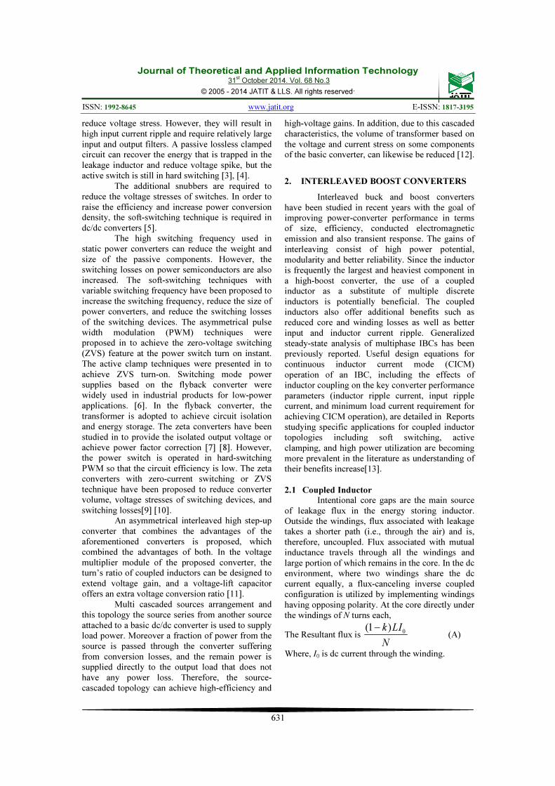
From the above literature the power & voltage rating are properly mentioned in this paper and more important of this circuit is coupled inductor. In this coupled inductor working benefits is achieving a high voltage gain about 10 times of input voltage, so that the coupled inductor is useful of one of the voltage lift technique for the converter. It has two same rating of capacitor value, one capacitor is parallel with source side and another one capacitor is parallel with load side, but both of the capacitors are useful for continuous supply to the load.
4. OPERATION OF THE PROPOSED
CONVERTER
The operation of the boost converter is
explained as following four modes and the proposed converter has given on figure 1.
Figure 1: Circuit Configuration Of The Proposed
Converter
MODE I: (t=t0 to t1 for S1 & t=t2 to t3 for S2)
In this transition interval, from the figure 2 the switch S1 is going to turned ON at t=0 but S2 is already maintained conduction is to be extended to reach at t=t3 the L2 is fully energised and C1 also got fully charged but L1 have 1/3 level of energy stored in the Inductor L1 at t=t1. In this mode 1 duration C2 capacitor discharge the energy to the load. Diodes D1 and D2 are turned OFF, so supply voltage is not present on the output load.
Figure 2: The Mode 1 Circuit Diagram
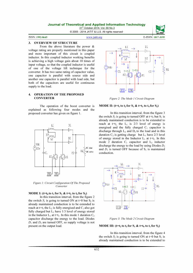
MODE II: (t=t1 to t2 for S1 & t=t3 to t4 for S2)
In this transition interval, from the figure 3 the switch S2 is going to turned OFF at t=t3 but S1 is already maintained conduction is to be extended to reach at t=t2, the L1 is 2/3 level of energy is energised and the fully charged C1 capacitor is discharge through L2 and D2 to the load and in this duration C2 is getting charge but L1 have 2/3 level of energy stored in the Inductor L1 at t=t2. In this mode 2 duration C1 capacitor and L2 inductor discharge the energy to the load by using Diodes D2 and D1 is turned OFF because of S1 is maintained conduction.
Figure 3: The Mode 2 Circuit Diagram
MODE III: (t=t2 to t3 for S1 & t=t0 to t1 for S2)
In this transition interval, from the figure 4 the switch S2 is going to turned ON at t=0 but S1 is already maintained conduction is to be extended to
Journal of Theoretical and Applied Information Technology 31
st October 2014. Vol. 68 No.3
© 2005 - 2014 JATIT & LLS. All rights reserved.
ISSN: 1992-8645 www.jatit.org E-ISSN: 1817-3195
633
reach at t=t3 the L1 is fully energised and C1 also got fully charged but L2 have 1/3 level of energy stored in the Inductor L2 at t=t1. In this mode 1 duration C2 capacitor discharge the energy to the load. Diodes D1 and D2 are turned OFF, so supply voltage is not present on the output load.
Figure 4: The Mode 3 Circuit Diagram
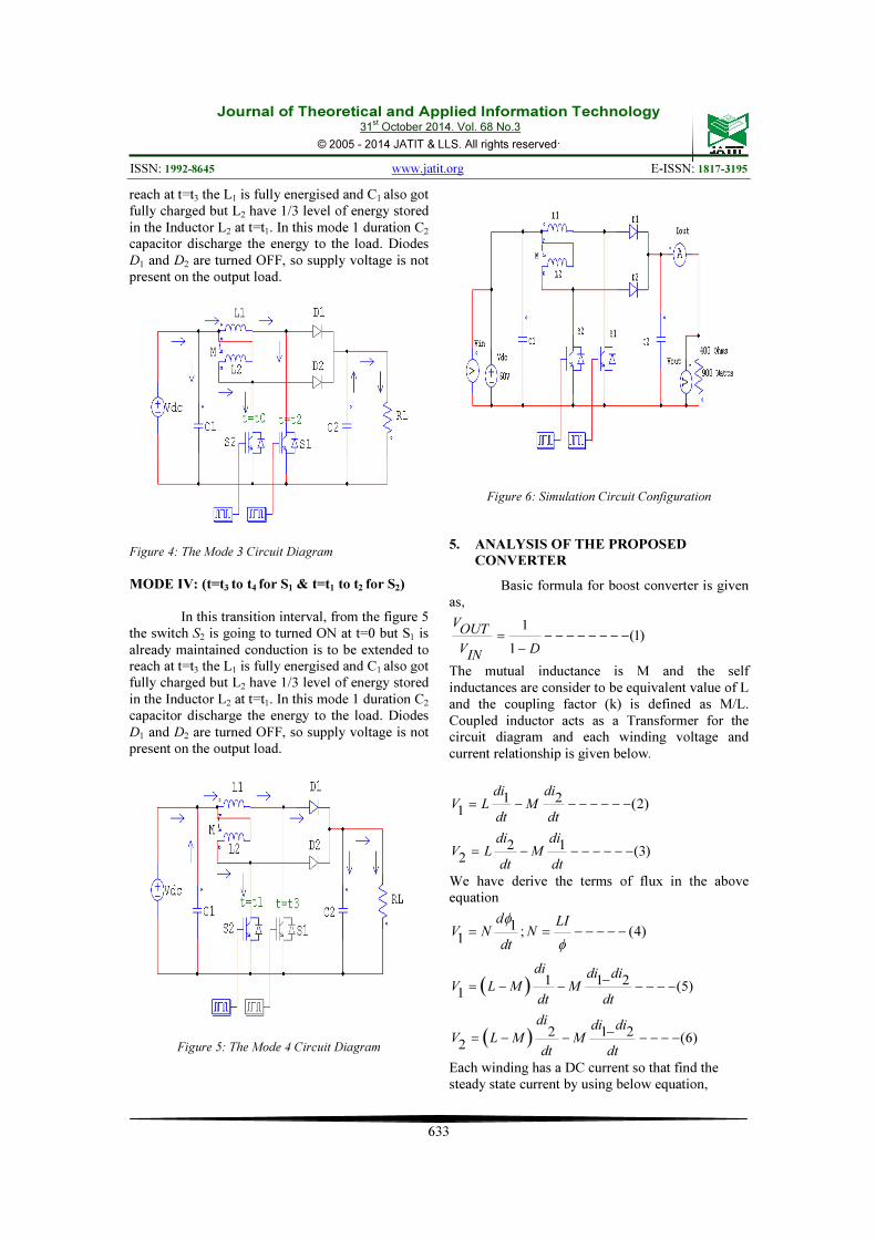
MODE IV: (t=t3 to t4 for S1 & t=t1 to t2 for S2)
In this transition interval, from the figure 5 the switch S2 is going to turned ON at t=0 but S1 is already maintained conduction is to be extended to reach at t=t3 the L1 is fully energised and C1 also got fully charged but L2 have 1/3 level of energy stored in the Inductor L2 at t=t1. In this mode 1 duration C2 capacitor discharge the energy to the load. Diodes D1 and D2 are turned OFF, so supply voltage is not present on the output load.
Figure 5: The Mode 4 Circuit Diagram
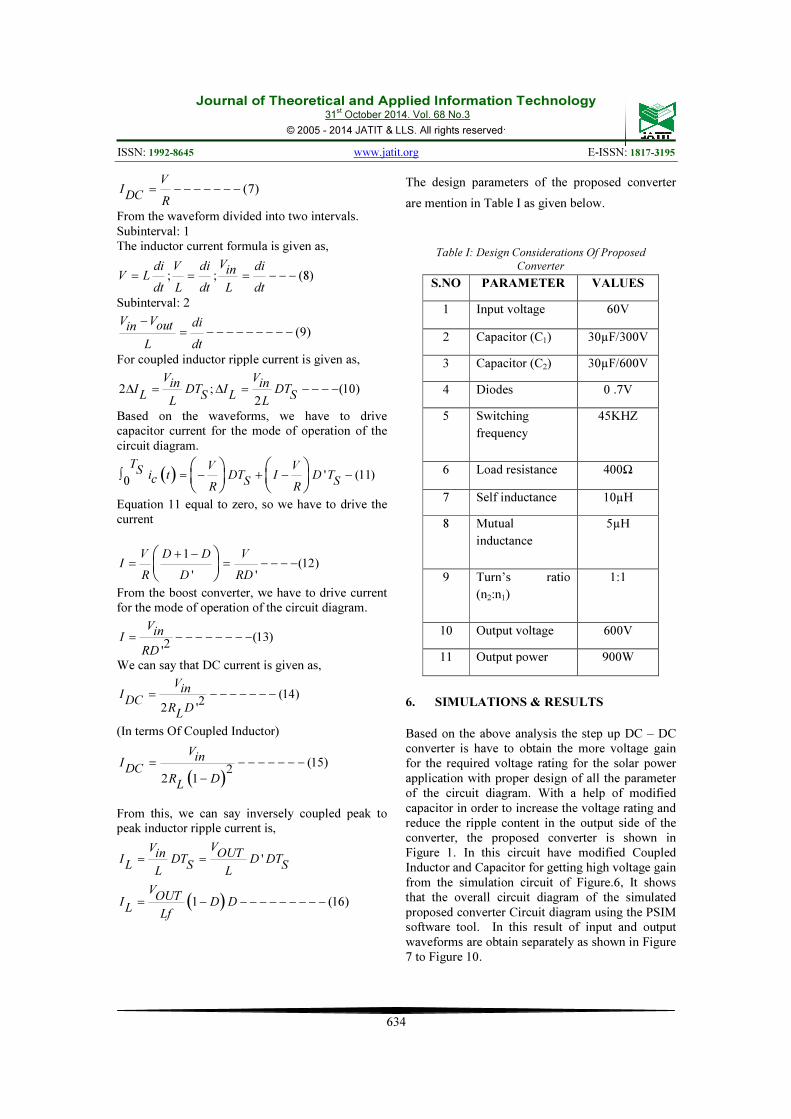
Figure 6: Simulation Circuit Configuration
5. ANALYSIS OF THE PROPOSED
CONVERTER
Basic formula for boost converter is given as,
1(1)
1
VOUT
V DIN
= − − − − − − − −
−
The mutual inductance is M and the self inductances are consider to be equivalent value of L and the coupling factor (k) is defined as M/L. Coupled inductor acts as a Transformer for the circuit diagram and each winding voltage and current relationship is given below.
1 2 (2)1
di di
V L M
dt dt
= − − − − − − −
2 1 (3)2
di di
V L M
dt dt
= − − − − − − −
We have derive the terms of flux in the above equation
1 ; (4)1
d LIV N N
dt
φ
φ= = − − − − −
( ) 1 1 2 (5)1
di di di
V L M M
dt dt
−= − − − − − −
( ) 2 1 2 (6)2
di di di
V L M M
dt dt
−= − − − − − −
Each winding has a DC current so that find the steady state current by using below equation,
Journal of Theoretical and Applied Information Technology 31
st October 2014. Vol. 68 No.3
© 2005 - 2014 JATIT & LLS. All rights reserved.
ISSN: 1992-8645 www.jatit.org E-ISSN: 1817-3195
634
(7)V
IDC
R
= − − − − − − −
From the waveform divided into two intervals. Subinterval: 1 The inductor current formula is given as,
; ; (8)Vdi V di diin
V L
dt L dt L dt
= = = − − −
Subinterval: 2
(9)V V dioutin
L dt
−
= − − − − − − − − −
For coupled inductor ripple current is given as,
2 ; (10)2
V Vin in
I DT I DTL LS S
L L
∆ = ∆ = − − − −
Based on the waveforms, we have to drive capacitor current for the mode of operation of the circuit diagram.
( ) ' (11)0
T V VSi t DT I D Tc S S
R R
∫ = − + − −
Equation 11 equal to zero, so we have to drive the current
1(12)
' '
V D D VI
R D RD
+ −
= = − − − −
From the boost converter, we have to drive current for the mode of operation of the circuit diagram.
(13)2'
Vin
I
RD
= − − − − − − − −
We can say that DC current is given as,
(14)2
2 '
Vin
IDC
R DL
= − − − − − − −
(In terms Of Coupled Inductor)
( )(15)
22 1
Vin
IDC
R DL
= − − − − − − −
−
From this, we can say inversely coupled peak to peak inductor ripple current is,
'
VVin OUT
I DT D DTL S S
L L
= =
( )1 (16)VOUTI D DLLf
= − − − − − − − − − −
The design parameters of the proposed converter
are mention in Table I as given below.
Table I: Design Considerations Of Proposed
Converter
S.NO PARAMETER VALUES
1 Input voltage 60V
2 Capacitor (C1) 30µF/300V
3 Capacitor (C2) 30µF/600V
4 Diodes 0 .7V
5 Switching
frequency
45KHZ
6 Load resistance 400Ω
7 Self inductance 10µH
8 Mutual
inductance
5µH
9 Turn’s ratio
(n2:n1)
1:1
10 Output voltage 600V
11 Output power 900W
6. SIMULATIONS & RESULTS
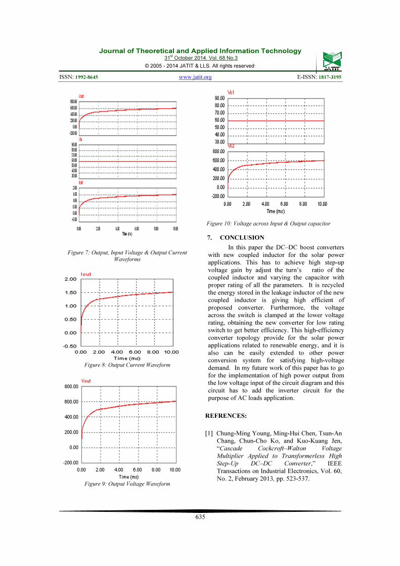
Based on the above analysis the step up DC – DC converter is have to obtain the more voltage gain for the required voltage rating for the solar power application with proper design of all the parameter of the circuit diagram. With a help of modified capacitor in order to increase the voltage rating and reduce the ripple content in the output side of the converter, the proposed converter is shown in Figure 1. In this circuit have modified Coupled Inductor and Capacitor for getting high voltage gain from the simulation circuit of Figure.6, It shows that the overall circuit diagram of the simulated proposed converter Circuit diagram using the PSIM software tool. In this result of input and output waveforms are obtain separately as shown in Figure 7 to Figure 10.
Journal of Theoretical and Applied Information Technology 31
st October 2014. Vol. 68 No.3
© 2005 - 2014 JATIT & LLS. All rights reserved.
ISSN: 1992-8645 www.jatit.org E-ISSN: 1817-3195
635
Figure 7: Output, Input Voltage & Output Current
Waveforms
Figure 8: Output Current Waveform
Figure 9: Output Voltage Waveform
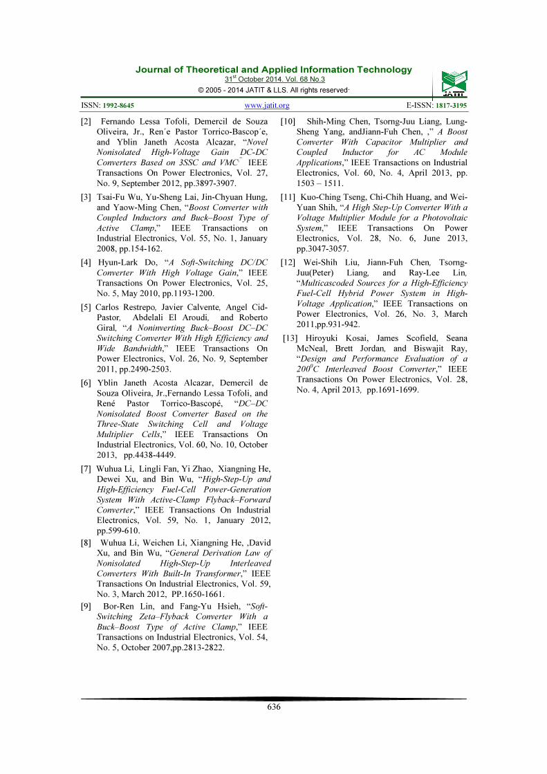
Figure 10: Voltage across Input & Output capacitor
7. CONCLUSION
In this paper the DC–DC boost converters with new coupled inductor for the solar power applications. This has to achieve high step-up voltage gain by adjust the turn’s ratio of the coupled inductor and varying the capacitor with proper rating of all the parameters. It is recycled the energy stored in the leakage inductor of the new coupled inductor is giving high efficient of proposed converter. Furthermore, the voltage across the switch is clamped at the lower voltage rating, obtaining the new converter for low rating switch to get better efficiency. This high-efficiency converter topology provide for the solar power applications related to renewable energy, and it is also can be easily extended to other power conversion system for satisfying high-voltage demand. In my future work of this paper has to go for the implementation of high power output from the low voltage input of the circuit diagram and this circuit has to add the inverter circuit for the purpose of AC loads application.
REFRENCES:
[1] Chung-Ming Young, Ming-Hui Chen, Tsun-An Chang, Chun-Cho Ko, and Kuo-Kuang Jen, “Cascade Cockcroft–Walton Voltage
Multiplier Applied to Transformerless High
Step-Up DC–DC Converter,” IEEE Transactions on Industrial Electronics, Vol. 60, No. 2, February 2013, pp. 523-537.
Journal of Theoretical and Applied Information Technology 31
st October 2014. Vol. 68 No.3
© 2005 - 2014 JATIT & LLS. All rights reserved.
ISSN: 1992-8645 www.jatit.org E-ISSN: 1817-3195
636
[2] Fernando Lessa Tofoli, Demercil de Souza Oliveira, Jr., Ren´e Pastor Torrico-Bascop´e, and Yblin Janeth Acosta Alcazar, “Novel
Nonisolated High-Voltage Gain DC-DC
Converters Based on 3SSC and VMC,” IEEE
Transactions On Power Electronics, Vol. 27,
No. 9, September 2012, pp.3897-3907.
[3] Tsai-Fu Wu, Yu-Sheng Lai, Jin-Chyuan Hung, and Yaow-Ming Chen, “Boost Converter with
Coupled Inductors and Buck–Boost Type of
Active Clamp,” IEEE Transactions on Industrial Electronics, Vol. 55, No. 1, January
2008, pp.154-162.
[4] Hyun-Lark Do, “A Soft-Switching DC/DC
Converter With High Voltage Gain,” IEEE Transactions On Power Electronics, Vol. 25, No. 5, May 2010, pp.1193-1200.
[5] Carlos Restrepo, Javier Calvente, Angel Cid-Pastor, Abdelali El Aroudi, and Roberto Giral, “A Noninverting Buck–Boost DC–DC
Switching Converter With High Efficiency and
Wide Bandwidth,” IEEE Transactions On Power Electronics, Vol. 26, No. 9, September
2011, pp.2490-2503.
[6] Yblin Janeth Acosta Alcazar, Demercil de Souza Oliveira, Jr.,Fernando Lessa Tofoli, and René Pastor Torrico-Bascopé, “DC–DC
Nonisolated Boost Converter Based on the
Three-State Switching Cell and Voltage
Multiplier Cells,” IEEE Transactions On Industrial Electronics, Vol. 60, No. 10, October 2013, pp.4438-4449.
[7] Wuhua Li, Lingli Fan, Yi Zhao, Xiangning He, Dewei Xu, and Bin Wu, “High-Step-Up and
High-Efficiency Fuel-Cell Power-Generation
System With Active-Clamp Flyback–Forward
Converter,” IEEE Transactions On Industrial Electronics, Vol. 59, No. 1, January 2012, pp.599-610.
[8] Wuhua Li, Weichen Li, Xiangning He, ,David Xu, and Bin Wu, “General Derivation Law of
Nonisolated High-Step-Up Interleaved
Converters With Built-In Transformer,” IEEE Transactions On Industrial Electronics, Vol. 59, No. 3, March 2012, PP.1650-1661.
[9] Bor-Ren Lin, and Fang-Yu Hsieh, “Soft-
Switching Zeta–Flyback Converter With a
Buck–Boost Type of Active Clamp,” IEEE Transactions on Industrial Electronics, Vol. 54, No. 5, October 2007,pp.2813-2822.
[10] Shih-Ming Chen, Tsorng-Juu Liang, Lung-Sheng Yang, andJiann-Fuh Chen, ,” A Boost
Converter With Capacitor Multiplier and
Coupled Inductor for AC Module
Applications,” IEEE Transactions on Industrial Electronics, Vol. 60, No. 4, April 2013, pp.
1503 – 1511.
[11] Kuo-Ching Tseng, Chi-Chih Huang, and Wei-Yuan Shih, “A High Step-Up Converter With a
Voltage Multiplier Module for a Photovoltaic
System,” IEEE Transactions On Power Electronics, Vol. 28, No. 6, June 2013,
pp.3047-3057.
[12] Wei-Shih Liu, Jiann-Fuh Chen, Tsorng-Juu(Peter) Liang, and Ray-Lee Lin, “Multicascoded Sources for a High-Efficiency
Fuel-Cell Hybrid Power System in High-
Voltage Application,” IEEE Transactions on Power Electronics, Vol. 26, No. 3, March 2011,pp.931-942.
[13] Hiroyuki Kosai, James Scofield, Seana McNeal, Brett Jordan, and Biswajit Ray, “Design and Performance Evaluation of a
2000C Interleaved Boost Converter,” IEEE
Transactions On Power Electronics, Vol. 28,
No. 4, April 2013, pp.1691-1699.