Embed Size (px)
Citation preview
ASAHI KASEI [AK2346B]
AK2346B
Two-way Radio Audio Processor
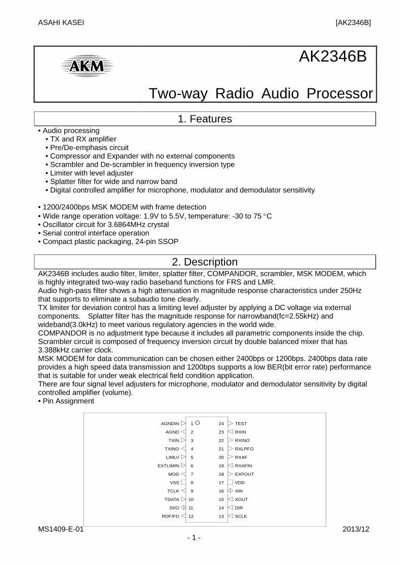
1. Features • Audio processing
• TX and RX amplifier • Pre/De-emphasis circuit • Compressor and Expander with no external components • Scrambler and De-scrambler in frequency inversion type • Limiter with level adjuster • Splatter filter for wide and narrow band • Digital controlled amplifier for microphone, modulator and demodulator sensitivity
• 1200/2400bps MSK MODEM with frame detection • Wide range operation voltage: 1.9V to 5.5V, temperature: -30 to 75 °C • Oscillator circuit for 3.6864MHz crystal • Serial control interface operation • Compact plastic packaging, 24-pin SSOP
2. Description AK2346B includes audio filter, limiter, splatter filter, COMPANDOR, scrambler, MSK MODEM, which is highly integrated two-way radio baseband functions for FRS and LMR. Audio high-pass filter shows a high attenuation in magnitude response characteristics under 250Hz that supports to eliminate a subaudio tone clearly. TX limiter for deviation control has a limiting level adjuster by applying a DC voltage via external components. Splatter filter has the magnitude response for narrowband(fc=2.55kHz) and wideband(3.0kHz) to meet various regulatory agencies in the world wide. COMPANDOR is no adjustment type because it includes all parametric components inside the chip. Scrambler circuit is composed of frequency inversion circuit by double balanced mixer that has 3.388kHz carrier clock. MSK MODEM for data communication can be chosen either 2400bps or 1200bps. 2400bps data rate provides a high speed data transmission and 1200bps supports a low BER(bit error rate) performance that is suitable for under weak electrical field condition application. There are four signal level adjusters for microphone, modulator and demodulator sensitivity by digital controlled amplifier (volume). • Pin Assignment
AGNDIN
AGND
TXIN
TXINO
LIMLV
EXTLIMIN
MOD
VSS
TCLK
TDATA
DI/O
RDF/FD
11
12
1
2
3
4
5
6
7
8
9
10
TEST
RXIN
RXINO
RXLPFO
RXAF
RXAFIN
EXPOUT
VDD
XIN
XOUT
DIR
SCLK
24
23
22
21
20
19
18
17
16
15
14
13
MS1409-E-01 2013/12 - 1 -
ASAHI KASEI [AK2346B]
3. Contents 1. Features ............................................................................................................................... 1 2. Description ........................................................................................................................... 1 3. Contents .............................................................................................................................. 2 4. Block Diagram ..................................................................................................................... 3 5. Circuit Configuration ............................................................................................................ 4 6. Pin/Function ......................................................................................................................... 5 7. Absolute Maximum Ratings ................................................................................................. 7 8. Recommended Operating Conditions .................................................................................. 7 9. Digital DC characteristics ..................................................................................................... 7 10. Power Consumption........................................................................................................... 8 11. Analog characteristics ........................................................................................................ 9 12. Level Diagram .................................................................................................................. 14 13. Serial Interface Configuration .......................................................................................... 15 14. Digital AC timing .............................................................................................................. 20 15. MSK MODEM Description ............................................................................................... 23 16. Recommended External Application Circuits ................................................................... 26 17. Packaging ........................................................................................................................ 30 18. Important Notice............................................................................................................... 31
MS1409-E-01 2013/12 - 2 -
ASAHI KASEI [AK2346B]
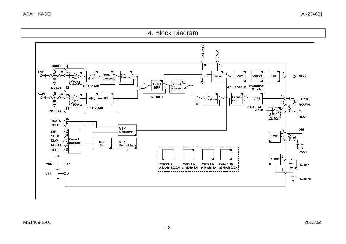
4. Block Diagram
MS1409-E-01 2013/12 - 3 -
[AK2346B]
5. Circuit Configuration
Block Description
TXA1
The operational amplifier for transmit audio gain adjustment and for the filter to eliminate aliasing noise by the SCF(switched capacitor filter) in the following stage. Please select an external resistor and capacitor to set the gain less than 30dB and the cut-off frequency to about 10kHz.
VR1 (HPF)
Digitally controlled amplifier (volume) for transmit audio signal level which is adjustable in 1.5dB steps over a –6.0dB to +4.5dB range by setting VR12 to VR10 register.
Compressor The circuit to compress transmits audio signal level by 1/2 in dB scale. Standard cross-point is –10dBx. TC register sets OFF/ON to the circuit.
Pre-emphasis The circuit to emphasis the high-frequency component of transmit audio signal to improve S/N ratio of the modulation signal.
TX/RXHPF The High-pass filter to eliminate the low-frequency component less than 250Hz for transmit and receive audio signal.
Scrambler/ Descrambler
Scramble/De-scramble circuit to inverse transmit and receive audio spectrum by 3.388kHz carrier signal. EM and PCONT register can set scramble/De-scramble or Emphasis circuit. Both circuits do not use simultaneously.
Limiter An amplitude limiting circuit to suppress the frequency deviation of the modulation signal. The limitation level can be adjusted by applying a DC voltage to the LIMLV pin. If the LIMLV pin is open, the limitation level is applied to a predetermined level.
Splatter The circuit to eliminate the high frequency component higher than 3kHz included in the limiter output signal or the MSK modulator signal. The cut-off frequency can be selected by SPL register.
VR2 Digitally controlled amplifier (volume) for MOD output level which is adjustable in 0.2dB steps over a –3.2dB to +3.0dB range by setting VR25 to VR20 register. VR25 is a –6/0dB coarse bit.
SMF The smoothing filter to eliminate the high frequency and clock component caused in SCF circuits.
RXA1 The operational amplifier for receives audio gain adjustment and for the filter to eliminate aliasing noise by the SCF in the following stage. Please select an external resistor and capacitor to set the gain less than 20dB and the cut-off frequency to about 40kHz.
VR3 Digitally controlled amplifier (volume) for receive audio signal level which is adjustable in 0.5dB steps over a –4.0dB to +3.5dB range by setting VR33 to VR30 register.
RXLPF The Low-pass filter to eliminate the high frequency component higher than 3kHz for receive audio signal.
De-emphasis The circuit to de-emphasis the emphasized signal by pre-emphasis circuit.
Expander The circuit to expand the receive audio signal level to double in dB scale compressed by compressor Standard cross-point is –10dBx. TC register sets OFF/ON to the circuit.
VR4 Digitally controlled amplifier (volume) for EXPOUT output level which is adjustable in 1.5dB, steps over a –18dB and –4.5dB to +4.5dB range by setting VR42 to VR40 register.
RXA2 The operational amplifier used on smoothing filter to eliminate clock component included in EXPOUT output signal. Please set the gain to 0dB and the cut-off frequency to about 20kHz by external resistor and capacitor.
MSK Modulator The circuit to generate a MSK signal according to the received digital data from TDATA pin.
MSK BPF The Band-pass filter to eliminate the low and high frequency component for received MSK signal.
MSK Demodulator The circuit to reproduce the 1200/2400bps receive clock and data from MSK signal at RXIN pin.
MS1409-E-01 2013/12 - 4 -
[AK2346B]
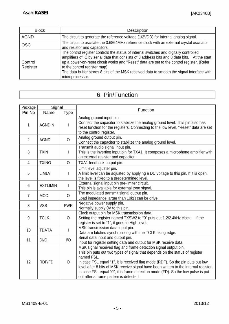
Block Description AGND The circuit to generate the reference voltage (1/2VDD) for internal analog signal.
OSC The circuit to oscillate the 3.6864MHz reference clock with an external crystal oscillator and resistor and capacitors.
Control Register
The control register controls the status of internal switches and digitally controlled amplifiers of IC by serial data that consists of 3 address bits and 8 data bits. At the start up a power-on-reset circuit works and “Reset” data are set to the control register. (Refer to the control register map) The data buffer stores 8 bits of the MSK received data to smooth the signal interface with microprocessor.
6. Pin/Function
Package Signal Function Pin No Name Type
1 AGNDIN I
Analog ground input pin. Connect the capacitor to stabilize the analog ground level. This pin also has reset function for the registers. Connecting to the low level, “Reset” data are set to the control register.
2 AGND O Analog ground output pin. Connect the capacitor to stabilize the analog ground level.
3 TXIN I Transmit audio signal input pin. This is the inverting input pin for TXA1. It composes a microphone amplifier with an external resister and capacitor.
4 TXINO O TXA1 feedback output pin.
5 LIMLV I Limit level adjuster pin. A limit level can be adjusted by applying a DC voltage to this pin. If it is open, the level is fixed to a predetermined level.
6 EXTLIMIN I External signal input pin pre-limiter circuit. This pin is available for external tone signal.
7 MOD O The modulated transmit signal output pin. Load impedance larger than 10kΩ can be drive.
8 VSS PWR Negative power supply pin. Normally supply 0V to this pin.
9 TCLK O Clock output pin for MSK transmission data. Setting the register named TXSW2 to “0” puts out 1.2/2.4kHz clock. If the register is set to “1”, it goes to High level.
10 TDATA I MSK transmission data input pin. Data are latched synchronizing with the TCLK rising edge.
11 DI/O I/O Serial data input and output pin. Input for register setting data and output for MSK receive data.
12 RDF/FD O
MSK signal received flag and frame detection signal output pin. This pin puts out two types of signal that depends on the status of register named FSL. In case FSL equal “1”, it is received flag mode (RDF). So the pin puts out low level after 8 bits of MSK receive signal have been written to the internal register. In case FSL equal “0”, it is frame detection mode (FD). So the low pulse is put out after a frame pattern is detected.
MS1409-E-01 2013/12 - 5 -
[AK2346B]
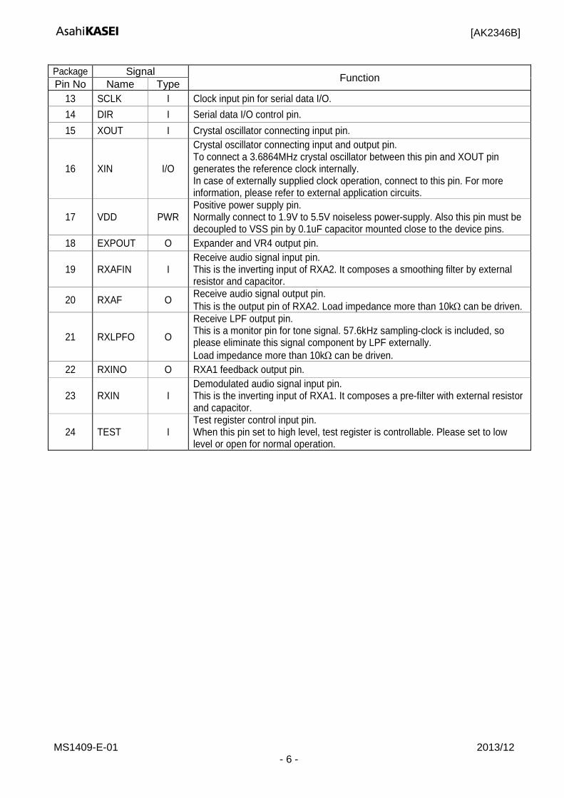
Package Signal Function Pin No Name Type
13 SCLK I Clock input pin for serial data I/O. 14 DIR I Serial data I/O control pin. 15 XOUT I Crystal oscillator connecting input pin.
16 XIN I/O
Crystal oscillator connecting input and output pin. To connect a 3.6864MHz crystal oscillator between this pin and XOUT pin generates the reference clock internally. In case of externally supplied clock operation, connect to this pin. For more information, please refer to external application circuits.
17 VDD PWR Positive power supply pin. Normally connect to 1.9V to 5.5V noiseless power-supply. Also this pin must be decoupled to VSS pin by 0.1uF capacitor mounted close to the device pins.
18 EXPOUT O Expander and VR4 output pin.
19 RXAFIN I Receive audio signal input pin. This is the inverting input of RXA2. It composes a smoothing filter by external resistor and capacitor.
20 RXAF O Receive audio signal output pin. This is the output pin of RXA2. Load impedance more than 10kΩ can be driven.
21 RXLPFO O
Receive LPF output pin. This is a monitor pin for tone signal. 57.6kHz sampling-clock is included, so please eliminate this signal component by LPF externally. Load impedance more than 10kΩ can be driven.
22 RXINO O RXA1 feedback output pin.
23 RXIN I Demodulated audio signal input pin. This is the inverting input of RXA1. It composes a pre-filter with external resistor and capacitor.
24 TEST I Test register control input pin. When this pin set to high level, test register is controllable. Please set to low level or open for normal operation.
MS1409-E-01 2013/12 - 6 -
[AK2346B]
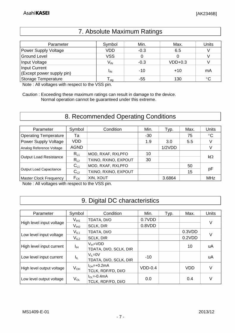
7. Absolute Maximum Ratings
Parameter Symbol Min. Max. Units Power Supply Voltage VDD -0.3 6.5 V Ground Level VSS 0 0 V Input Voltage VIN -0.3 VDD+0.3 V Input Current (Except power supply pin) IIN -10 +10 mA
Storage Temperature Tstg -55 130 °C Note : All voltages with respect to the VSS pin. Caution : Exceeding these maximum ratings can result in damage to the device.
Normal operation cannot be guaranteed under this extreme.
8. Recommended Operating Conditions
Parameter Symbol Condition Min. Typ. Max. Units Operating Temperature Ta -30 75 °C Power Supply Voltage VDD 1.9 3.0 5.5 V Analog Reference Voltage AGND 1/2VDD V
Output Load Resistance RL1 MOD, RXAF, RXLPFO 10
kΩ RL2 TXINO, RXINO, EXPOUT 30
Output Load Capacitance CL1 MOD, RXAF, RXLPFO 50
pF CL2 TXINO, RXINO, EXPOUT 15 Master Clock Frequency FCK XIN, XOUT 3.6864 MHz Note : All voltages with respect to the VSS pin.
9. Digital DC characteristics
Parameter Symbol Condition Min. Typ. Max. Units
High level input voltage VIH1 TDATA, DI/O 0.7VDD
V VIH2 SCLK, DIR 0.8VDD
Low level input voltage VIL1 TDATA, DI/O 0.3VDD
V VIL2 SCLK, DIR 0.2VDD
High level input current IIH VIH=VDD TDATA, DI/O, SCLK, DIR
10 uA
Low level input current IIL VIL=0V TDATA, DI/O, SCLK, DIR
-10 uA
High level output voltage VOH IOH=+0.2mA TCLK, RDF/FD, DI/O
VDD-0.4 VDD V
Low level output voltage VOL IOL=-0.4mA TCLK, RDF/FD, DI/O
0.0 0.4 V
MS1409-E-01 2013/12 - 7 -
[AK2346B]
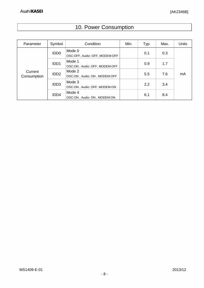
10. Power Consumption
Parameter Symbol Condition Min. Typ. Max. Units
Current Consumption
IDD0 Mode 0 OSC:OFF, Audio: OFF, MODEM:OFF
0.1 0.3
mA
IDD1 Mode 1 OSC:ON , Audio: OFF, MODEM:OFF
0.9 1.7
IDD2 Mode 2 OSC:ON , Audio: ON , MODEM:OFF
5.5 7.6
IDD3 Mode 3 OSC:ON , Audio: OFF, MODEM:ON
2.2 3.4
IDD4 Mode 4 OSC:ON , Audio: ON , MODEM:ON
6.1 8.4
MS1409-E-01 2013/12 - 8 -
[AK2346B]
11. Analog characteristics For the following conditions unless otherwise specified: f=1kHz, Emphasis: on, COMPANDOR: on, Scrambler: off, VR1=VR2=VR3=VR4=0dB with the external circuit shown in example page.26 to 29. “dBx” is standardized unit for 1.9V to 5.5V operation, 0dBx=-5+20log(VDD/2)dBm, 0dBm=0.775Vrms.
1) TX Audio System
Parameter Condition Min. Typ. Max. Units Notes Standard Input Level @TXINO -10 dBx
Absolute Gain TXINO to MOD -1.5 0 +1.5 dB Limit Level
EXTLIMIN to MOD Without external R adjustment With external R adjustment
-8.6 -7.6
-6.6 -6.6
dBx
Compressor Linearity
TXINO to MOD TXINO=-44dBx TXINO=-50dBx Relative value to 0dB for MOD level of -10dBx TXINO.
-20.0 -24.0
-17.0 -20.0
-14.0 -16.0 dB
Compressor Distortion
TXINO to MOD TXINO=-10dBx 30kHz Low-pass filtering
-35 dB
Noise Level with no signal input
TXINO to MOD C-Message filtering
-36.5 dBm
VR1 Attenuation Error
TXINO to MOD -6.0 dB to 4.5dB, 1.5dB/step -1.5 +1.5 dB
VR2 ATT Error (VR24,23,22,21,20)
TXINO to MOD -3.2dB to +3.0dB, 0.2dB/step -0.2 +0.2 dB
VR2 ATT Error (VR25=0)
TXINO to MOD Relative error for -6/0dB -6.4 -6 -5.6 dB
2) RX Audio System
Parameter Condition Min. Typ. Max. Units Notes Standard Input Level @RXINO -10 dBx
Absolute Gain RXINO to RXLPFO -1.5 0 +1.5 dB RXINO to RXAF -1.5 0 +1.5 dB
Expander Linearity
RXINO to RXAF RXINO=-25dBx RXINO=-30dBx Relative value to 0dB for RXAF level of -10dBx RXINO
-33.0 -45.0
-30.0 -40.0
-27.0 -35.0 dB
Expander Distortion
RXINO to RXAF RXINO=-5dBx 30kHz Low-pass filtering
-35 dB
Noise Level with no signal input
RXINO to RXAF C-Message Filtering
-70 dBm
VR3 Attenuation Error
RXIN0 to RXAF -4.0dB to +3.5dB, 0.5dB/step -0.5 +0.5 dB
VR4 Attenuation Error
RXIN0 to RXAF -4.5 to +4.5dB, 1.5dB/step -1.5 +1.5 dB
VR4 ATT Error (VR42,41,40=0,0,0)
RXIN0 to RXAF Relative error for -18/0dB -20 -18 -16 dB
MS1409-E-01 2013/12 - 9 -
[AK2346B]
3) Audio Filter Characteristics 3.1) Emphasis: off, COMPANDOR: off, Scrambler: off (Design target values)
Parameter Condition Min. Typ. Max. Units Notes TX overall characteristics
TXINO to MOD Relative value to gain at 1kHz
250Hz -50 -38 dB 300Hz to 2.0kHz
2.5kHz 3.0kHz 6.0kHz
-1.0 -1.5 -4.0
-32
+1.0 +1.0 -1.0 -28
dB SPL=0 fc=2.55K
300Hz to 2.5kHz 3.0kHz 6.0kHz
-1.0 -1.5
-26
+1.0 +1.0 -22
dB SPL=1 fc=3.0K
RX overall characteristics
RXINO to RXAF
Relative value to gain at 1kHz
250Hz 300Hz
350Hz to 3.0kHz 6.0kHz
-1.5 -1.0
-49
-38
-38 +1.0 +1.0 -28
dB
3.2) Emphasis: on, COMPANDOR: off, Scrambler: off
Parameter Condition Min. Typ. Max. Units Notes TX overall characteristics
TXINO to MOD Relative value to gain at 1kHz
250Hz -57 -40 dB 300Hz 2.5kHz 3.0kHz 6.0kHz
-12.5 +6.0 +4.5
-23
-9.5 +9.0 +8.5 -18
dB SPL=0 fc=2.55K
300Hz 2.5kHz 3.0kHz 6.0kHz
-12.5 +6.0 +7.0
-17
-9.5 +9.0
+10.5 -12
dB SPL=1 fc=3.0K
RX overall characteristics
RXINO to RXAF
Relative value to gain at 1kHz
250Hz 300Hz 3.0kHz 6.0kHz
+8.5 -11.5
-38
-52
-26 +11.5 -8.5 -40
dB
MS1409-E-01 2013/12 - 10 -
[AK2346B]
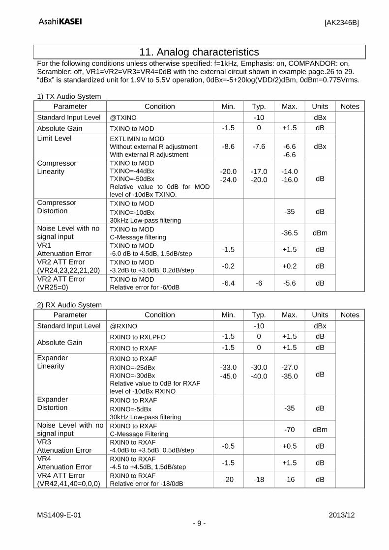
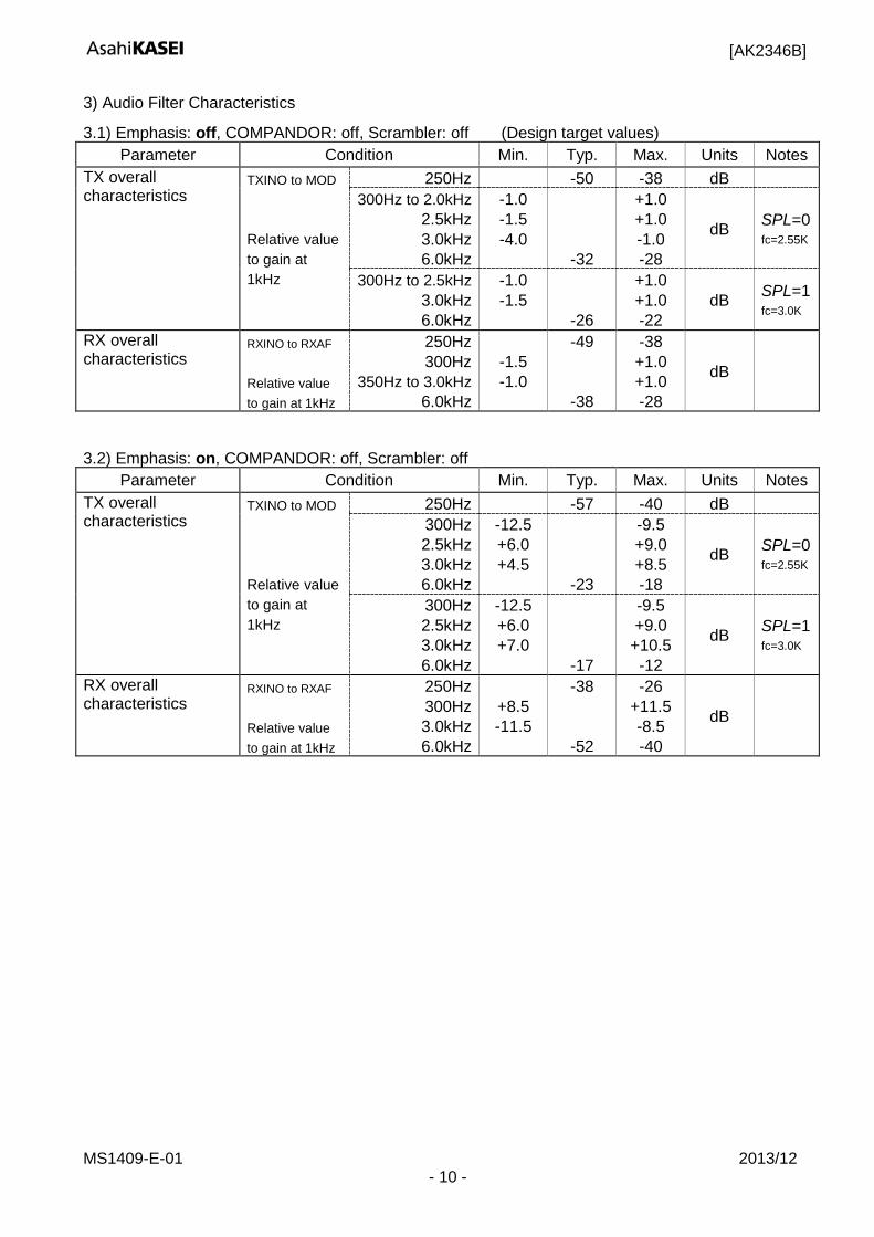
• Audio path frequency response (Emphasis:off)
Figure 1: TX overall response without pre-emphasis.
Figure 2: RX overall response without de-emphasis.
-60
-50
-40
-30
-20
-10
0
10
20
1.E+02 1.E+03 1.E+04
FREQUENCY(Hz)
GA
IN(d
B)
SPL=0SPL=1
-60
-50
-40
-30
-20
-10
0
10
20
1.E+02 1.E+03 1.E+04
FREQUENCY(Hz)
GA
IN(d
B)
MS1409-E-01 2013/12 - 11 -
[AK2346B]
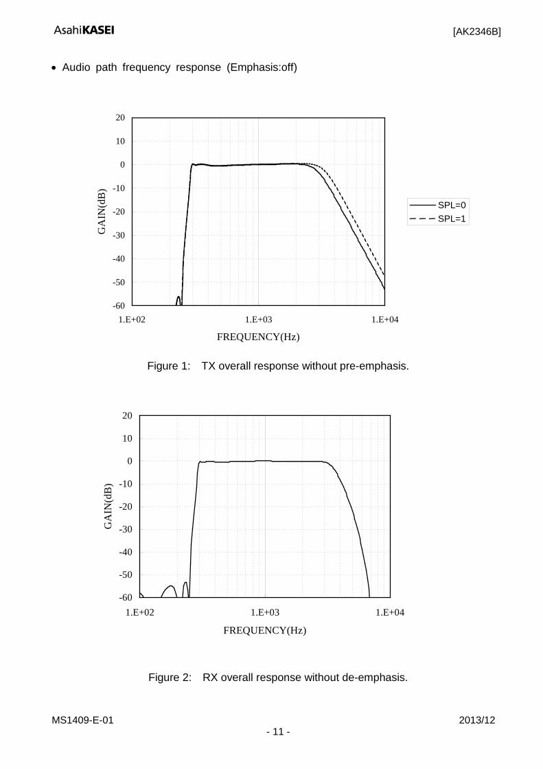
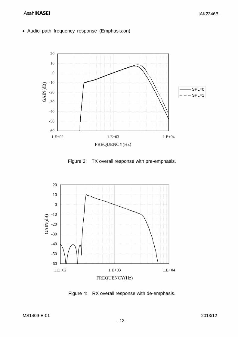
• Audio path frequency response (Emphasis:on)
Figure 3: TX overall response with pre-emphasis.
Figure 4: RX overall response with de-emphasis.
-60
-50
-40
-30
-20
-10
0
10
20
1.E+02 1.E+03 1.E+04
FREQUENCY(Hz)
GA
IN(d
B)
SPL=0SPL=1
-60
-50
-40
-30
-20
-10
0
10
20
1.E+02 1.E+03 1.E+04
FREQUENCY(Hz)
GA
IN(d
B)
MS1409-E-01 2013/12 - 12 -
[AK2346B]
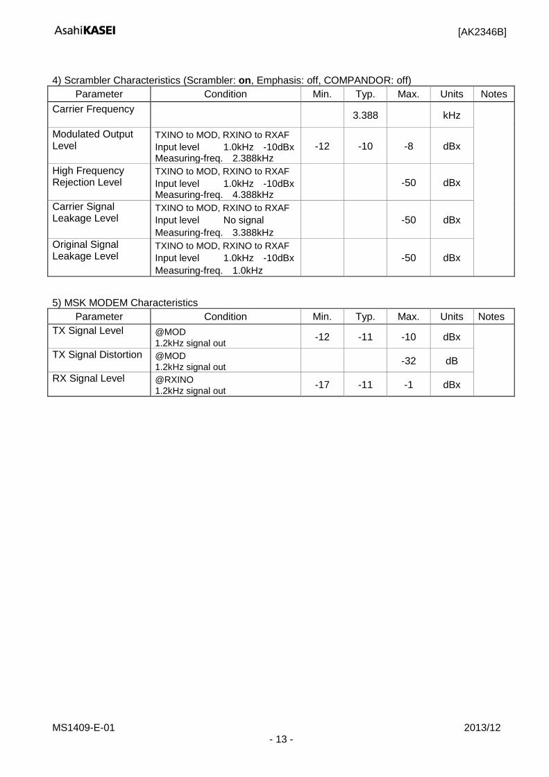
4) Scrambler Characteristics (Scrambler: on, Emphasis: off, COMPANDOR: off)
Parameter Condition Min. Typ. Max. Units Notes Carrier Frequency
3.388 kHz
Modulated Output Level
TXINO to MOD, RXINO to RXAF Input level 1.0kHz -10dBx Measuring-freq. 2.388kHz
-12 -10 -8 dBx
High Frequency Rejection Level
TXINO to MOD, RXINO to RXAF Input level 1.0kHz -10dBx Measuring-freq. 4.388kHz
-50 dBx
Carrier Signal Leakage Level
TXINO to MOD, RXINO to RXAF Input level No signal Measuring-freq. 3.388kHz
-50 dBx
Original Signal Leakage Level
TXINO to MOD, RXINO to RXAF Input level 1.0kHz -10dBx Measuring-freq. 1.0kHz
-50 dBx
5) MSK MODEM Characteristics
Parameter Condition Min. Typ. Max. Units Notes TX Signal Level
@MOD 1.2kHz signal out -12 -11 -10 dBx
TX Signal Distortion
@MOD 1.2kHz signal out -32 dB
RX Signal Level @RXINO 1.2kHz signal out -17 -11 -1 dBx
MS1409-E-01 2013/12 - 13 -
[AK2346B]
12. Level Diagram 1) TX audio system : TXRX=0 2) RX audio system : TXRX=1 “dBx” is standardized unit for 1.9V to 5.5V operation, 0dBx=-5+20log(VDD/2)dBm, 0dBm=0.775Vrms.
SMF Limitter Splatter +VR2
TXA1 VR1 Compressor Pre-emphasis TXHPF
MSK Modulator
Scrm /Descrm
10
0
-10
-20
-30
-40
-50
-60
-70
-80
-90
TXINO
+4.5 -6.0 dB 0 +3.0
-9.2 dB 0 Crosspoint -10dBx
0dB
0dB -7.6dBx
EXTLMIN
0
-10
-44
-50
-30
-27
-16
-5.5 -5
-10 -11
-7.0
-19.2 -11dBx (MSK)
-10dBx (Audio)
dBx
TXIN MOD
G = 30dB
-27dBx
-30dBx
0dB 0dB
f=1kHz
RXA2 Expander RXA1 VR3 RXLPF De-emphasis RXHPF
Scrm /Descrm
10
0
-10
-20
-25
-30
-40
-45
-50
-60
RXINO
+3.5 -4.0 dB 0 +4.5
-18.0 dB 0 Crosspoint -10dBx
-5dB
-5dB +5dB
EXPOUT
-5
-10
-25
-30
-25
-20 -14
-6.5
-5
0
-10 -5.5
-28
0dBx (Max.)
-10dBx (Typ.)
dBx
RXIN RXAF VR4
G = 20dB 0dB
RXLPFO
G = 0dB
-40dBx
-50dBx -50
-40
f=1kHz
MS1409-E-01 2013/12 - 14 -
[AK2346B]
13. Serial Interface Configuration 1) Register Configuration Address
Function Data
A2 A1 A0 D7 D6 D5 D4 D3 D2 D1 D0
0 0 0 Control register 1 BS3 BS2 BS1 TXRX TXSW2 TXSW1 RXSW FSL
0 0 1 Control register 2 - - TC EM PCONT SPL MSKSL FCLN
0 1 0 Volume register 1 - - - - - VR12 VR11 VR10
0 1 1 Volume register 2 - - VR25 VR24 VR23 VR22 VR21 VR20
1 0 0 Volume register 3 - VR33 VR32 VR31 VR30 VR42 VR41 VR40
1 0 1 MODEM register 1 Lower 8 bit of MODEM Flame pattern
1 1 0 MODEM register 2 Upper 8 bit of MODEM Flame pattern
1 1 1 Test register TST7 TST6 TST5 TST4 TST3 TST2 TST1 TST0
- - - MODEM register 3 MODEM Receive data
2) Register Map 2.1) Control Register 1
Address Data A2 A1 A0 D7 D6 D5 D4 D3 D2 D1 D0 0 0 0 BS3 BS2 BS1 TXRX TXSW2 TXSW1 RXSW FSL
Reset 0 0 0 1 1 1 1 1 2.1.1) Operation mode setting
BS3 BS2 BS1 Mode OSC, AGND TX, RX, Audio MODEM 0 0 0 Mode0 OFF OFF OFF 0 0 1 Mode1 ON OFF OFF 0 1 0 Mode2 ON ON OFF 0 1 1 Mode3 ON OFF ON 1 0/1 0/1 Mode4 ON ON ON
2.1.2) TX, RX Setting
Data Function Operation
Notes 0 1
TXRX TX, RX Switch TX Operation Note 1
RX Operation Note 2
Note 3
RXSW RX Audio Mute Active Note 4 FSL RDF/FD Switch FD enable RDF enable
2.1.3) TX audio path setting TXSW2 TXSW1 Operation Notes
0 0 External Tone Operation (EXTLIMIN --- Limiter --- Splatter)
0 1 MODEM Operation (MSK Modulator --- Splatter) 1 0 Audio Operation (HPF --- Limiter --- Splatter) 1 1 Mute (AGND --- Limiter --- Splatter)
MS1409-E-01 2013/12 - 15 -
[AK2346B]
Note 1: TXIN to EXPOUT path is available by setting TXRX=0 and RXSW=1 in register. However, Scrambler/Descrambler circuit does not work properly on this setting, so please set PCONT=1 (disable). To set RXSW=0 makes EXPOUT pin mute in operation. Note 2: RXIN to MOD path is available by setting TXRX=1 and TXSW2/TXSW1=1/0 in register. However, Scrambler/Descrambler circuit does not work properly on this setting, so please set PCONT=1 (disable). To set TXSW2/TXSW1=1/1 makes MOD pin mute in operation. Note 3: Please set a gain level properly in each circuit block according to level diagram in page 14. Note 4: RXLPFO pin does not be controlled by setting RXSW=0. It is normally active in RX mode. 2.2) Control Register 2
Address Data A2 A1 A0 D7 D6 D5 D4 D3 D2 D1 D0 0 0 1 - - TC EM PCONT SPL MSKSL FCLN
Reset - - 1 1 1 1 0 0
Data Function Operation
Notes 0 1
TC COMPANDOR OFF (disable) ON (enable)
SPL Splatter cut-off frequency 2.55kHz 3.0kHz
MSKSL MODEM data rate 2400bps 1200bps FCLN MODEM flame detect ON (enable) OFF (disable)
EM PCONT Operation Notes 1 1 Emphasis : ON (enable) Scrambler : OFF(disable) 0 1 Emphasis : OFF(disable) Scrambler : OFF(disable)
0/1 0 Emphasis : OFF(disable) Scrambler : ON (enable) 2.3) Volume Register 1
Address Data A2 A1 A0 D7 D6 D5 D4 D3 D2 D1 D0 0 1 0 - - - - - VR12 VR11 VR10
Reset - - - - - 1 0 0
VR12 VR11 VR10 VR1 Gain (dB) 0 0 0 -6.0 0 0 1 -4.5 0 1 0 -3.0 0 1 1 -1.5 1 0 0 0.0 1 0 1 +1.5 1 1 0 +3.0 1 1 1 +4.5
MS1409-E-01 2013/12 - 16 -
[AK2346B]
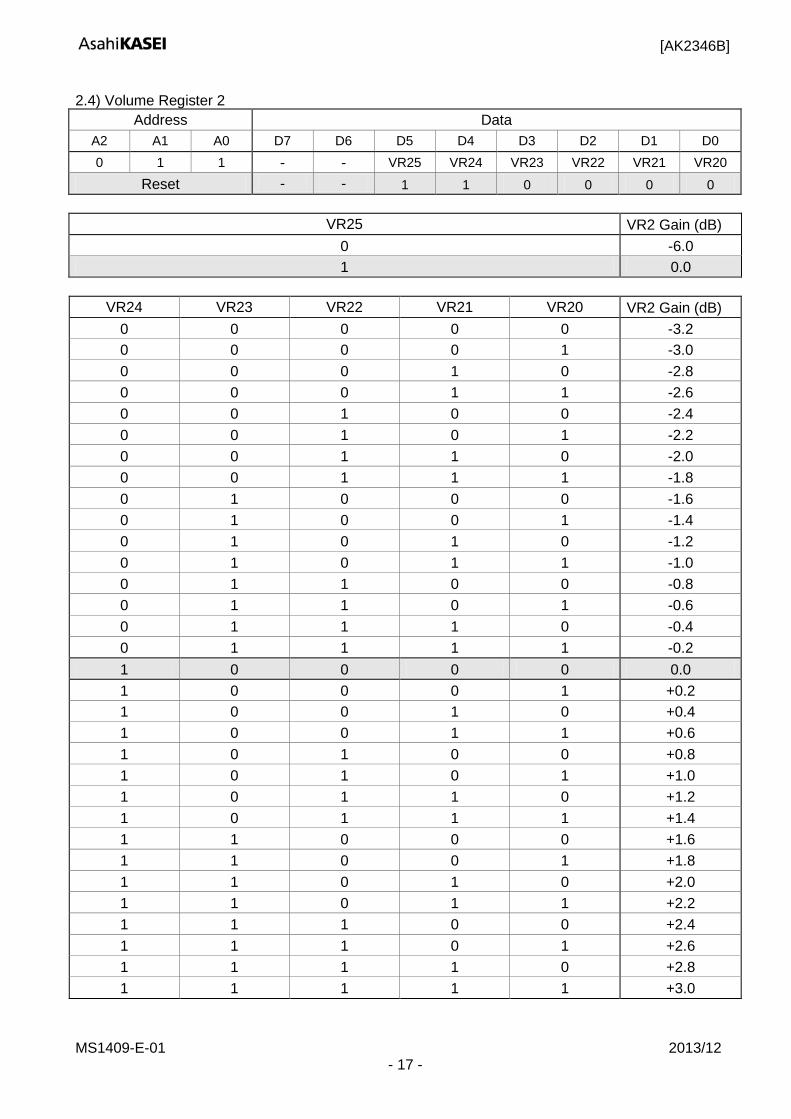
2.4) Volume Register 2
Address Data A2 A1 A0 D7 D6 D5 D4 D3 D2 D1 D0 0 1 1 - - VR25 VR24 VR23 VR22 VR21 VR20
Reset - - 1 1 0 0 0 0
VR25 VR2 Gain (dB) 0 -6.0 1 0.0
VR24 VR23 VR22 VR21 VR20 VR2 Gain (dB)
0 0 0 0 0 -3.2 0 0 0 0 1 -3.0 0 0 0 1 0 -2.8 0 0 0 1 1 -2.6 0 0 1 0 0 -2.4 0 0 1 0 1 -2.2 0 0 1 1 0 -2.0 0 0 1 1 1 -1.8 0 1 0 0 0 -1.6 0 1 0 0 1 -1.4 0 1 0 1 0 -1.2 0 1 0 1 1 -1.0 0 1 1 0 0 -0.8 0 1 1 0 1 -0.6 0 1 1 1 0 -0.4 0 1 1 1 1 -0.2 1 0 0 0 0 0.0 1 0 0 0 1 +0.2 1 0 0 1 0 +0.4 1 0 0 1 1 +0.6 1 0 1 0 0 +0.8 1 0 1 0 1 +1.0 1 0 1 1 0 +1.2 1 0 1 1 1 +1.4 1 1 0 0 0 +1.6 1 1 0 0 1 +1.8 1 1 0 1 0 +2.0 1 1 0 1 1 +2.2 1 1 1 0 0 +2.4 1 1 1 0 1 +2.6 1 1 1 1 0 +2.8 1 1 1 1 1 +3.0
MS1409-E-01 2013/12 - 17 -
[AK2346B]
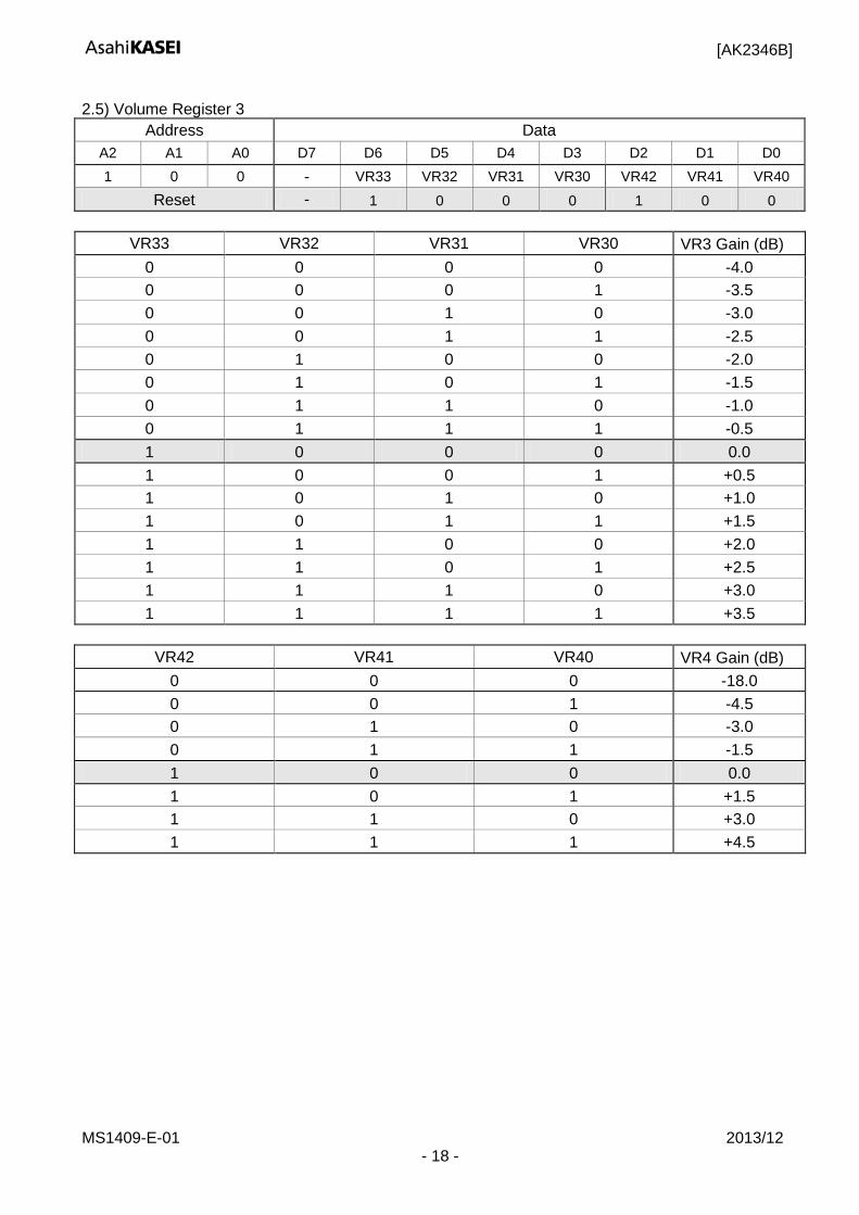
2.5) Volume Register 3
Address Data A2 A1 A0 D7 D6 D5 D4 D3 D2 D1 D0 1 0 0 - VR33 VR32 VR31 VR30 VR42 VR41 VR40
Reset - 1 0 0 0 1 0 0
VR33 VR32 VR31 VR30 VR3 Gain (dB) 0 0 0 0 -4.0 0 0 0 1 -3.5 0 0 1 0 -3.0 0 0 1 1 -2.5 0 1 0 0 -2.0 0 1 0 1 -1.5 0 1 1 0 -1.0 0 1 1 1 -0.5 1 0 0 0 0.0 1 0 0 1 +0.5 1 0 1 0 +1.0 1 0 1 1 +1.5 1 1 0 0 +2.0 1 1 0 1 +2.5 1 1 1 0 +3.0 1 1 1 1 +3.5
VR42 VR41 VR40 VR4 Gain (dB)
0 0 0 -18.0 0 0 1 -4.5 0 1 0 -3.0 0 1 1 -1.5 1 0 0 0.0 1 0 1 +1.5 1 1 0 +3.0 1 1 1 +4.5
MS1409-E-01 2013/12 - 18 -
[AK2346B]
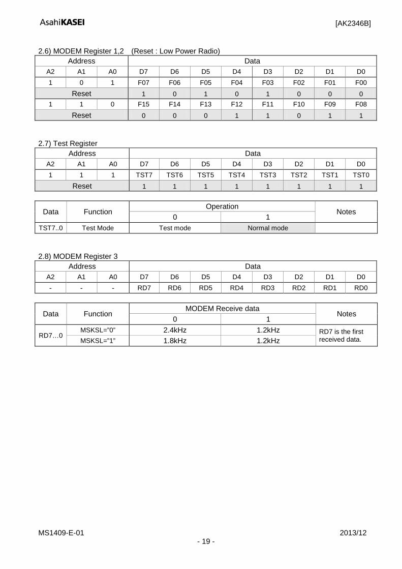
2.6) MODEM Register 1,2 (Reset : Low Power Radio)
Address Data A2 A1 A0 D7 D6 D5 D4 D3 D2 D1 D0 1 0 1 F07 F06 F05 F04 F03 F02 F01 F00
Reset 1 0 1 0 1 0 0 0 1 1 0 F15 F14 F13 F12 F11 F10 F09 F08
Reset 0 0 0 1 1 0 1 1 2.7) Test Register
Address Data A2 A1 A0 D7 D6 D5 D4 D3 D2 D1 D0 1 1 1 TST7 TST6 TST5 TST4 TST3 TST2 TST1 TST0
Reset 1 1 1 1 1 1 1 1
Data Function Operation
Notes 0 1
TST7..0 Test Mode Test mode Normal mode 2.8) MODEM Register 3
Address Data A2 A1 A0 D7 D6 D5 D4 D3 D2 D1 D0
- - - RD7 RD6 RD5 RD4 RD3 RD2 RD1 RD0
Data Function MODEM Receive data
Notes 0 1
RD7…0 MSKSL=”0” 2.4kHz 1.2kHz RD7 is the first
received data. MSKSL=”1” 1.8kHz 1.2kHz
MS1409-E-01 2013/12 - 19 -
[AK2346B]
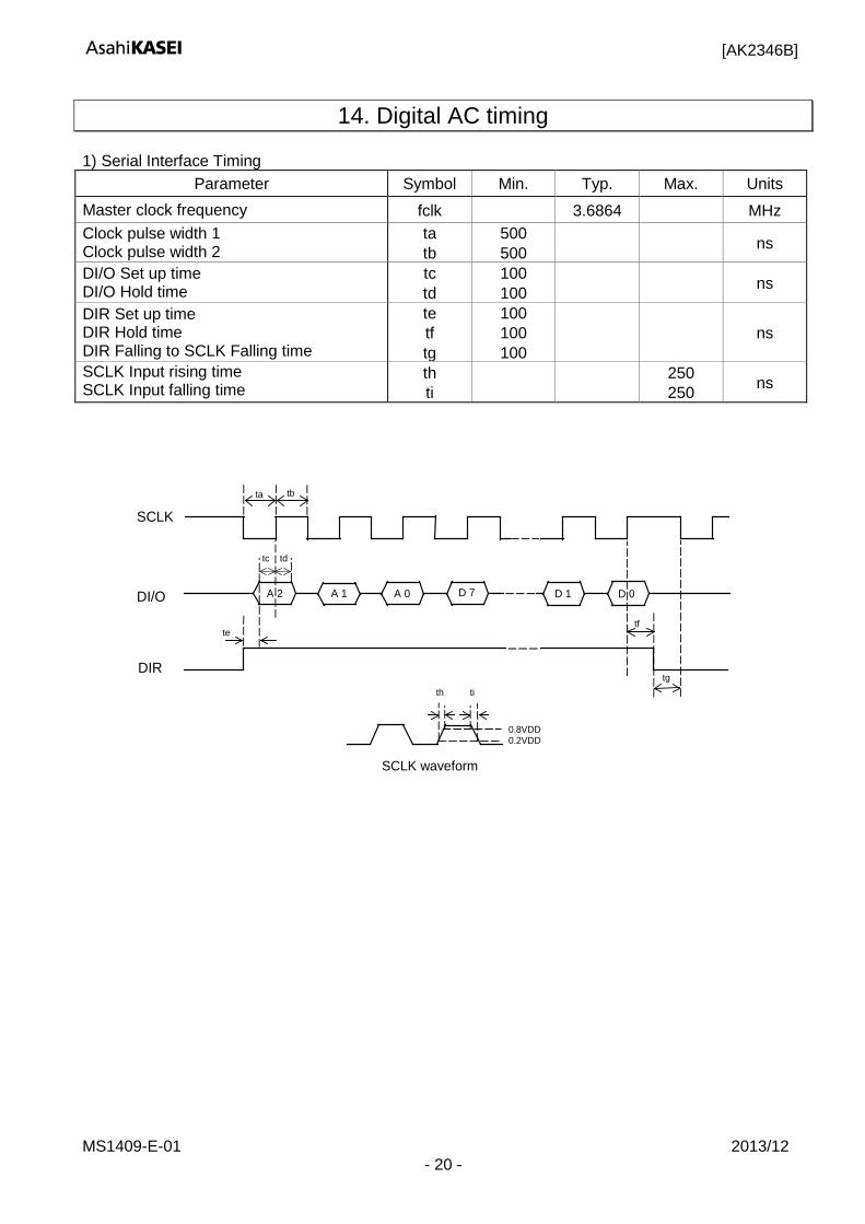
14. Digital AC timing 1) Serial Interface Timing
Parameter Symbol Min. Typ. Max. Units Master clock frequency fclk 3.6864 MHz Clock pulse width 1 Clock pulse width 2
ta tb
500 500 ns
DI/O Set up time DI/O Hold time
tc td
100 100 ns
DIR Set up time DIR Hold time DIR Falling to SCLK Falling time
te tf tg
100 100 100
ns
SCLK Input rising time SCLK Input falling time
th ti 250
250 ns
SCLK
DI/O
DIR
A 2 A 1 A 0 D 1 D 0
tf
tg
te
tb ta
0.8VDD 0.2VDD
ti th
SCLK waveform
D 7
tc td
MS1409-E-01 2013/12 - 20 -
[AK2346B]
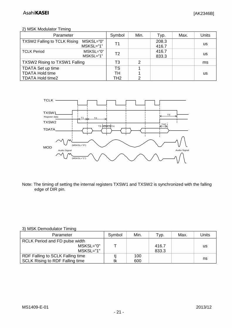
2) MSK Modulator Timing
Parameter Symbol Min. Typ. Max. Units TXSW2 Falling to TCLK Rising MSKSL=”0” MSKSL=”1” T1 208.3
416.7 us
TCLK Period MSKSL=”0” MSKSL=”1” T2 416.7
833.3 us
TXSW2 Rising to TXSW1 Falling T3 2 ms TDATA Set up time TDATA Hold time TDATA Hold time2
TS TH
TH2
1 1 2
us
Note: The timing of setting the internal registers TXSW1 and TXSW2 is synchronized with the falling
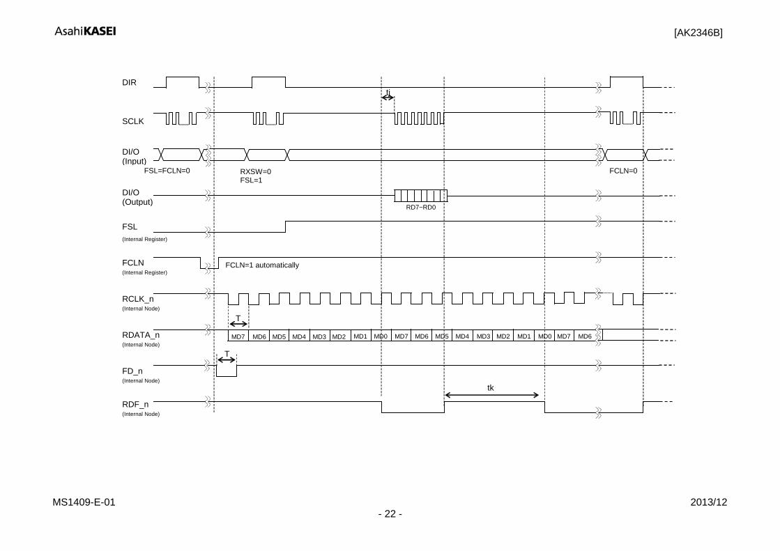
edge of DIR pin. 3) MSK Demodulator Timing
Parameter Symbol Min. Typ. Max. Units RCLK Period and FD pulse width
MSKSL=”0” MSKSL=”1”
T
416.7 833.3
us
RDF Falling to SCLK Falling time SCLK Rising to RDF Falling time
tj tk
100 600 ns
TCLK
TXSW1
TDATA TH TS
T1 T2
TXSW2
Audio Signal
(MSKSL=”0”)
(MSKSL=”1”)
Register data
TH2
T3
MOD Audio Signal
MS1409-E-01 2013/12 - 21 -
[AK2346B]
DIR
SCLK
DI/O (Input)
FSL
FCLN
(Internal Register)
(Internal Register)
RCLK_n (Internal Node)
RDATA_n
FD_n
RDF_n
DI/O (Output)
(Internal Node)
(Internal Node)
(Internal Node)
MD7 MD6 MD5 MD4 MD3 MD2 MD1 MD0 MD7 MD6 MD5 MD4 MD3 MD2 MD1 MD0 MD7 MD6
RXSW=0 FSL=1
FSL=FCLN=0
FCLN=1 automatically
FCLN=0
T
RD7~RD0
tj
tk
T
MS1409-E-01 2013/12 - 22 -
ASAHI KASEI [AK2346B]
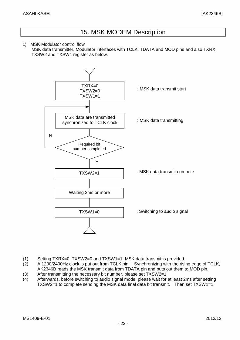
15. MSK MODEM Description 1) MSK Modulator control flow
MSK data transmitter, Modulator interfaces with TCLK, TDATA and MOD pins and also TXRX, TXSW2 and TXSW1 register as below.
(1) Setting TXRX=0, TXSW2=0 and TXSW1=1, MSK data transmit is provided. (2) A 1200/2400Hz clock is put out from TCLK pin. Synchronizing with the rising edge of TCLK,
AK2346B reads the MSK transmit data from TDATA pin and puts out them to MOD pin. (3) After transmitting the necessary bit number, please set TXSW2=1 (4) Afterwards, before switching to audio signal mode, please wait for at least 2ms after setting
TXSW2=1 to complete sending the MSK data final data bit transmit. Then set TXSW1=1.
: MSK data transmit compete
: Switching to audio signal
TXRX=0 TXSW2=0 TXSW1=1
Y
N
TXSW2=1
Waiting 2ms or more
TXSW1=0
Required bit number completed
: MSK data transmit start
: MSK data transmitting
Y
MSK data are transmitted synchronized to TCLK clock
MS1409-E-01 2013/12 - 23 -
ASAHI KASEI [AK2346B]
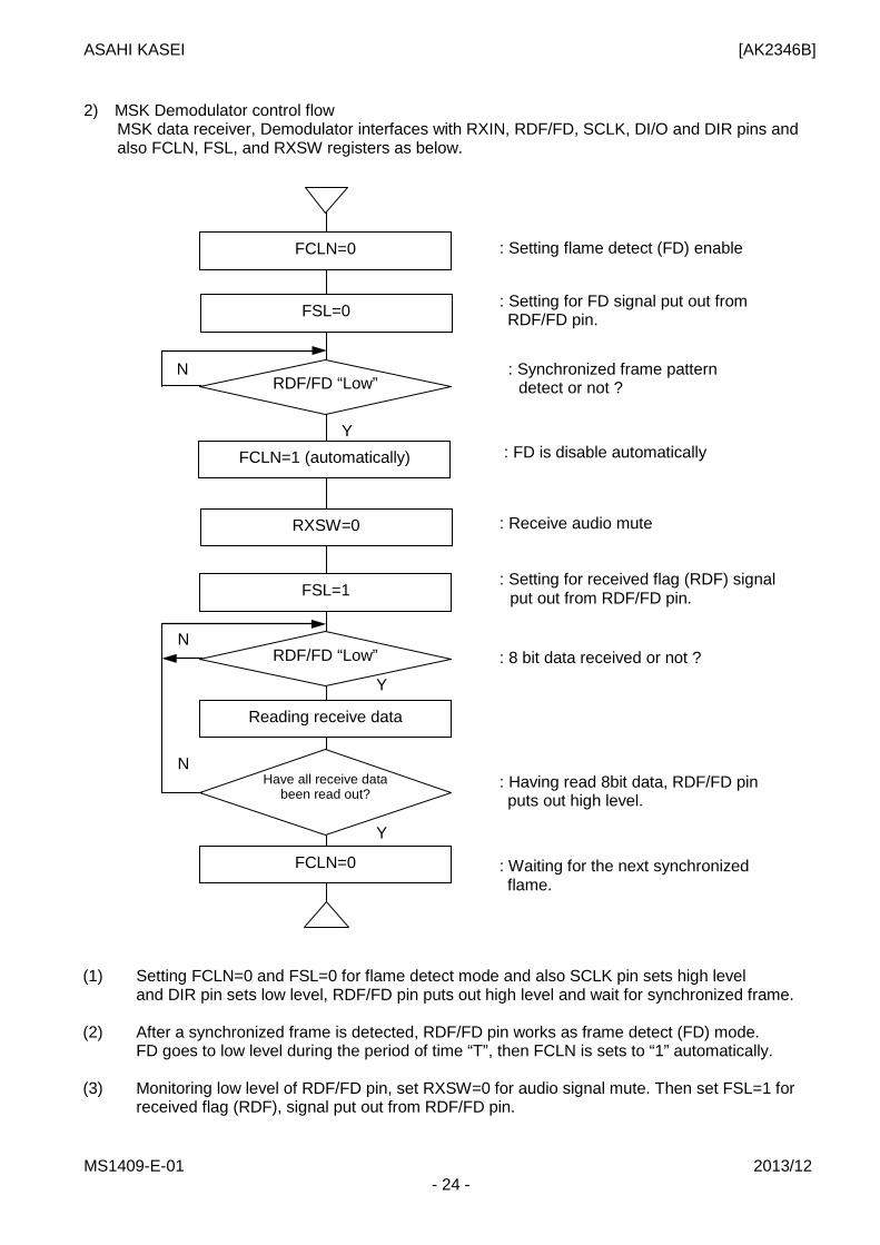
2) MSK Demodulator control flow
MSK data receiver, Demodulator interfaces with RXIN, RDF/FD, SCLK, DI/O and DIR pins and also FCLN, FSL, and RXSW registers as below.
(1) Setting FCLN=0 and FSL=0 for flame detect mode and also SCLK pin sets high level
and DIR pin sets low level, RDF/FD pin puts out high level and wait for synchronized frame.
(2) After a synchronized frame is detected, RDF/FD pin works as frame detect (FD) mode. FD goes to low level during the period of time “T”, then FCLN is sets to “1” automatically.
(3) Monitoring low level of RDF/FD pin, set RXSW=0 for audio signal mute. Then set FSL=1 for received flag (RDF), signal put out from RDF/FD pin.
: Waiting for the next synchronized flame.
: Having read 8bit data, RDF/FD pin puts out high level.
FCLN=0
RDF/FD “Low”
Y
N
RXSW=0
FSL=1
RDF/FD “Low”
Reading receive data
FCLN=0
Have all receive data been read out?
Y
: Setting for FD signal put out from RDF/FD pin.
: Synchronized frame pattern detect or not ?
: Receive audio mute
: 8 bit data received or not ? N
N
Y
FSL=0
FCLN=1 (automatically)
: Setting flame detect (FD) enable
: FD is disable automatically
: Setting for received flag (RDF) signal put out from RDF/FD pin.
MS1409-E-01 2013/12 - 24 -
ASAHI KASEI [AK2346B]
(4) After 8 bit received data (MD7…0) have been entered to the internal buffer from node RDATA,
RDF/FD pin goes to low level as RDF mode. (5) After CPU detects this low level at RDF/FD pin, please puts in 8 clock to SCLK pin. Then
modulated data (RD7…0) put out from DI/O pin synchronized with falling edge of SCLK clock.
(6) After 8 clock have been put into SCLK pin completely, RDF/FD pin goes to high level that shows all modulated data coming from DI/O pin.
(7) By repeating the steps (4), (5), (6), the data come out from DI/O pin continuously.
(8) After the necessary data have been read, DIR pin sets to high level and FCLN=0. Then
internal node RCLK and RDATA are set to “1” for initializing and system waits for the next synchronization frame data. This frame detection circuit does not have reset function. In case of stopping the sequence during the steps (1) to (8), please set again from the first step (1). Especially, when RDF/FD pin goes out low level on frame detecting, FCLN register is sets to “1” automatically as written in (2). If you set FCLN=0 during this operation, the date set “0” is ignored. So please set the data again after RDF/FD pin puts out high level. When frame detection is not used, please set FCLN=1 and FSL=1 from the beginning. In that case, monitoring the low level put out from RDF/FD pin, then puts 8 clock into the SCLK pin as written in step (4). In this sequence, please program the frame detecting operation by microprocessor.
MS1409-E-01 2013/12 - 25 -
ASAHI KASEI [AK2346B]
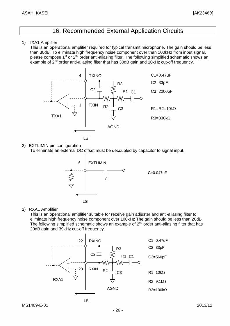
16. Recommended External Application Circuits 1) TXA1 Amplifier
This is an operational amplifier required for typical transmit microphone. The gain should be less than 30dB. To eliminate high frequency noise component over than 100kHz from input signal, please compose 1st or 2nd order anti-aliasing filter. The following simplified schematic shows an example of 2nd order anti-aliasing filter that has 30dB gain and 10kHz cut-off frequency.
2) EXTLIMIN pin configuration
To eliminate an external DC offset must be decoupled by capacitor to signal input. 3) RXA1 Amplifier
This is an operational amplifier suitable for receive gain adjuster and anti-aliasing filter to eliminate high frequency noise component over 100kHz The gain should be less than 20dB. The following simplified schematic shows an example of 2nd order anti-aliasing filter that has 20dB gain and 39kHz cut-off frequency.
LSI
EXTLIMIN
C
C=0.047uF
6
R3
C1=0.47uF
R1=10kΩ
_ +
LSI
C2
R1
RXA1
RXIN
RXINO
22
23
C3
C2=33pF
C1
R2
R2=9.1kΩ
R3=100kΩ
C3=560pF
AGND
R3
C1=0.47uF
R1=R2=10kΩ
_ +
LSI
C2
R1
TXA1
TXIN
TXINO
4
3
C3
C2=33pF
C1
R2
R3=330kΩ
C3=2200pF
AGND
MS1409-E-01 2013/12 - 26 -
ASAHI KASEI [AK2346B]
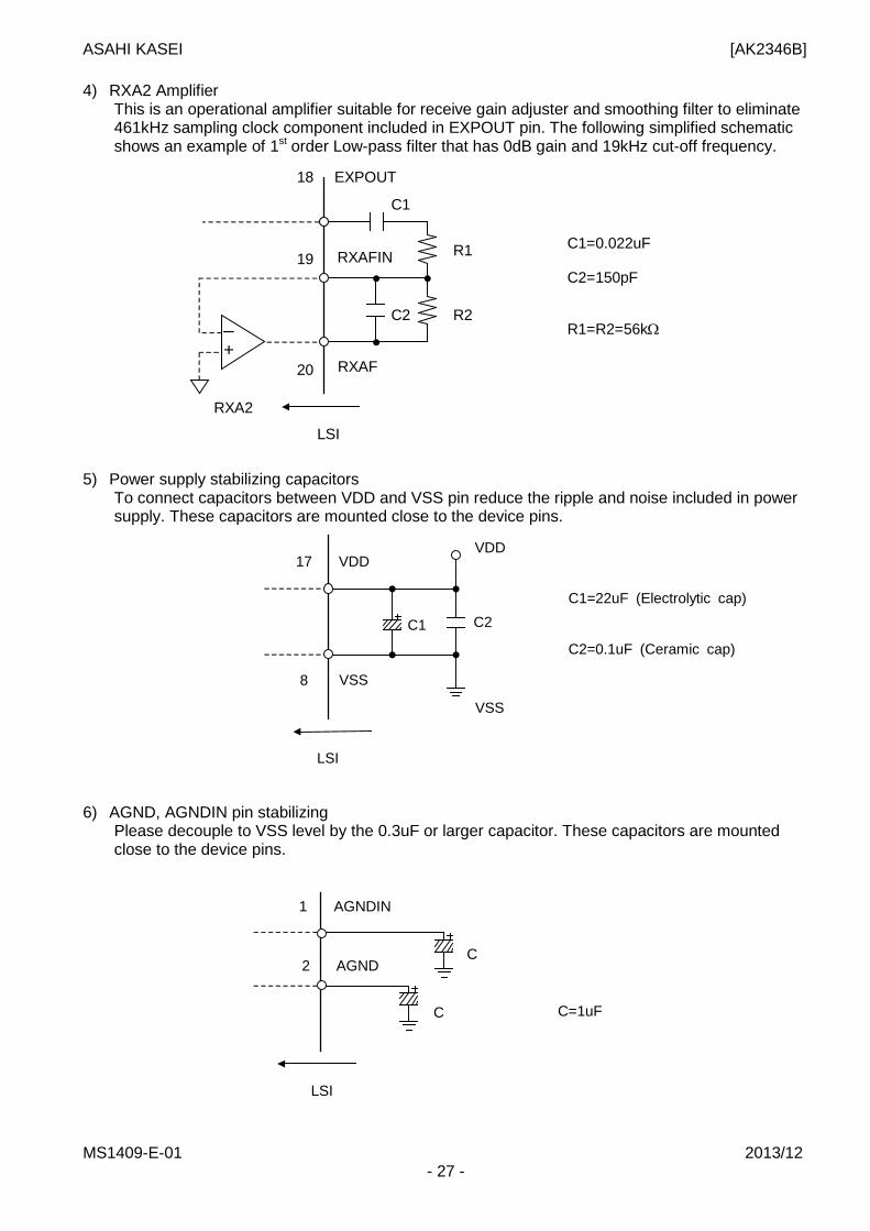
4) RXA2 Amplifier This is an operational amplifier suitable for receive gain adjuster and smoothing filter to eliminate 461kHz sampling clock component included in EXPOUT pin. The following simplified schematic shows an example of 1st order Low-pass filter that has 0dB gain and 19kHz cut-off frequency.
5) Power supply stabilizing capacitors
To connect capacitors between VDD and VSS pin reduce the ripple and noise included in power supply. These capacitors are mounted close to the device pins.
6) AGND, AGNDIN pin stabilizing
Please decouple to VSS level by the 0.3uF or larger capacitor. These capacitors are mounted close to the device pins.
AGNDIN
LSI
C
AGND
C
C=1uF
1
2
EXPOUT
R1
C1=0.022uF
R1=R2=56kΩ
_ +
LSI
C2
R2
RXA2
18
RXAF
RXAFIN
19
20
C1
C2=150pF
LSI
C2
VDD
VSS
C1
C1=22uF (Electrolytic cap)
C2=0.1uF (Ceramic cap)
VDD
VSS
17
8
MS1409-E-01 2013/12 - 27 -
ASAHI KASEI [AK2346B]
7) Clock Generation
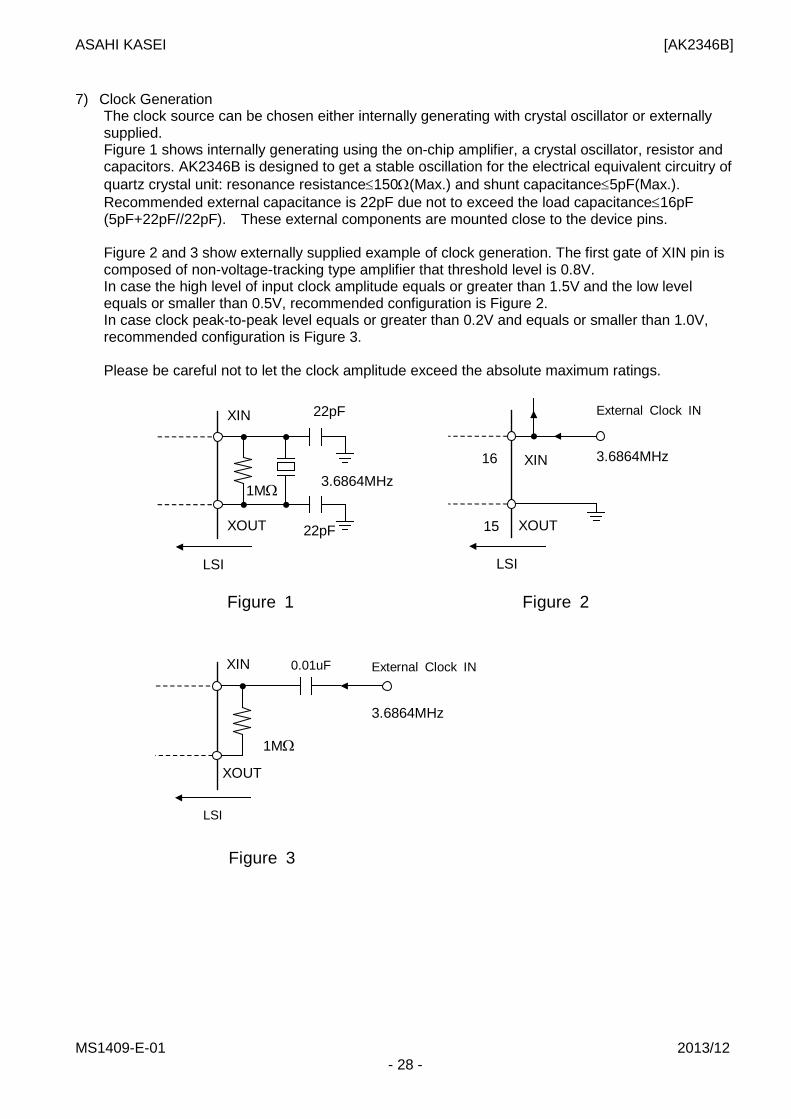
The clock source can be chosen either internally generating with crystal oscillator or externally supplied. Figure 1 shows internally generating using the on-chip amplifier, a crystal oscillator, resistor and capacitors. AK2346B is designed to get a stable oscillation for the electrical equivalent circuitry of quartz crystal unit: resonance resistance≤150Ω(Max.) and shunt capacitance≤5pF(Max.). Recommended external capacitance is 22pF due not to exceed the load capacitance≤16pF (5pF+22pF//22pF). These external components are mounted close to the device pins. Figure 2 and 3 show externally supplied example of clock generation. The first gate of XIN pin is composed of non-voltage-tracking type amplifier that threshold level is 0.8V. In case the high level of input clock amplitude equals or greater than 1.5V and the low level equals or smaller than 0.5V, recommended configuration is Figure 2. In case clock peak-to-peak level equals or greater than 0.2V and equals or smaller than 1.0V, recommended configuration is Figure 3. Please be careful not to let the clock amplitude exceed the absolute maximum ratings.
LSI
XIN
22pF
XOUT
1MΩ
22pF
3.6864MHz
Figure 1
Figure 3
LSI
XIN
0.01uF
XOUT
1MΩ
3.6864MHz
External Clock IN
LSI
XIN
XOUT
3.6864MHz
Figure 2
External Clock IN
16
15
MS1409-E-01 2013/12 - 28 -
ASAHI KASEI [AK2346B]
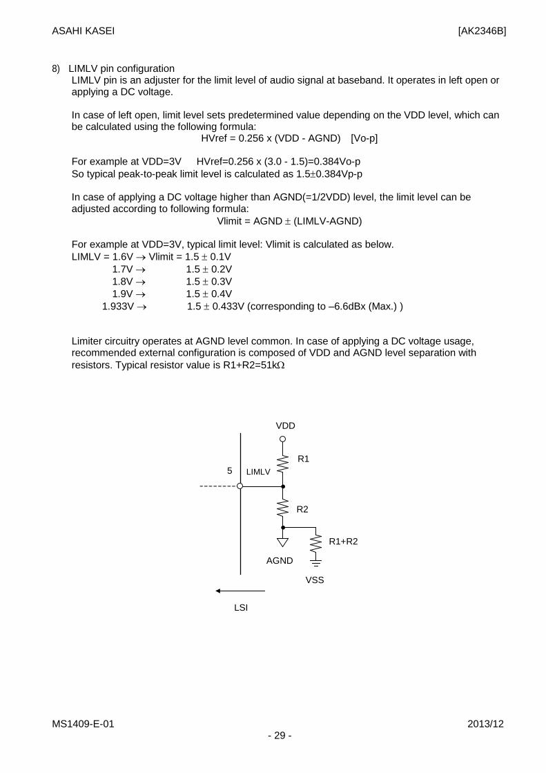
8) LIMLV pin configuration
LIMLV pin is an adjuster for the limit level of audio signal at baseband. It operates in left open or applying a DC voltage. In case of left open, limit level sets predetermined value depending on the VDD level, which can be calculated using the following formula:
HVref = 0.256 x (VDD - AGND) [Vo-p] For example at VDD=3V HVref=0.256 x (3.0 - 1.5)=0.384Vo-p So typical peak-to-peak limit level is calculated as 1.5±0.384Vp-p In case of applying a DC voltage higher than AGND(=1/2VDD) level, the limit level can be adjusted according to following formula:
Vlimit = AGND ± (LIMLV-AGND) For example at VDD=3V, typical limit level: Vlimit is calculated as below. LIMLV = 1.6V → Vlimit = 1.5 ± 0.1V 1.7V → 1.5 ± 0.2V 1.8V → 1.5 ± 0.3V 1.9V → 1.5 ± 0.4V 1.933V → 1.5 ± 0.433V (corresponding to –6.6dBx (Max.) ) Limiter circuitry operates at AGND level common. In case of applying a DC voltage usage, recommended external configuration is composed of VDD and AGND level separation with resistors. Typical resistor value is R1+R2=51kΩ
LSI
LIMLV
R1
VDD
VSS
R2
R1+R2
AGND
5
MS1409-E-01 2013/12 - 29 -
ASAHI KASEI [AK2346B]
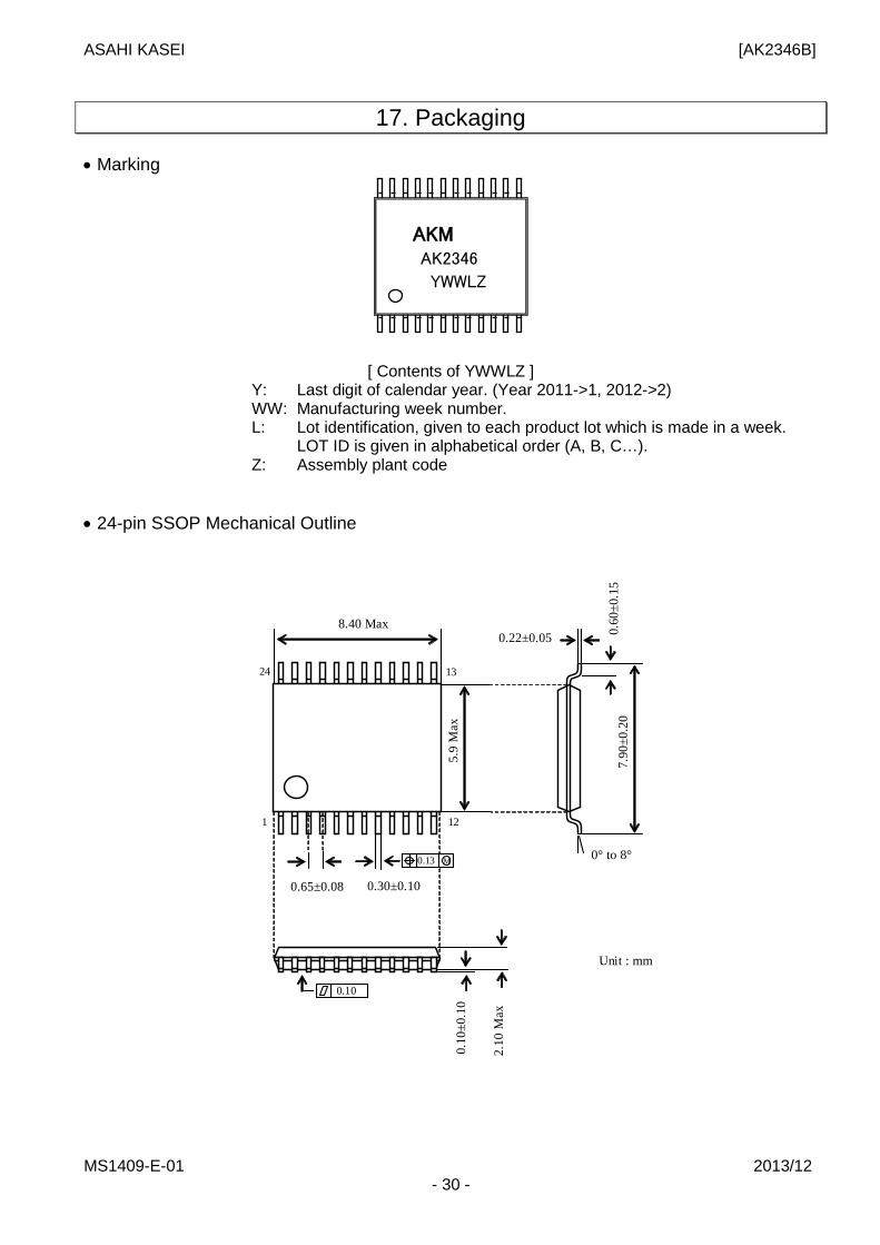
17. Packaging • Marking
[ Contents of YWWLZ ] Y: Last digit of calendar year. (Year 2011->1, 2012->2) WW: Manufacturing week number. L: Lot identification, given to each product lot which is made in a week.
LOT ID is given in alphabetical order (A, B, C…). Z: Assembly plant code
• 24-pin SSOP Mechanical Outline
AKM AK2346
YWWLZ
8.40 Max
Unit : mm
13 24
1 12
0.10
5.9
Max
0° to 8° 0.13 M
0.10
±0.1
0
2.10
Max
0.60
±0.1
5 7.
90±0
.20
0.65±0.08 0.30±0.10
0.22±0.05
MS1409-E-01 2013/12 - 30 -
ASAHI KASEI [AK2346B]
18. Important Notice
IMPORTANT NOTICE
0. Asahi Kasei Microdevices Corporation (“AKM”) reserves the right to make changes to the information contained in this document without notice. When you consider any use or application of AKM product stipulated in this document (“Product”), please make inquiries the sales office of AKM or authorized distributors as to current status of the Products.
1. All information included in this document are provided only to illustrate the operation and application examples of AKM Products. AKM neither makes warranties or representations with respect to the accuracy or completeness of the information contained in this document nor grants any license to any intellectual property rights or any other rights of AKM or any third party with respect to the information in this document. You are fully responsible for use of such information contained in this document in your product design or applications. AKM ASSUMES NO LIABILITY FOR ANY LOSSES INCURRED BY YOU OR THIRD PARTIES ARISING FROM THE USE OF SUCH INFORMATION IN YOUR PRODUCT DESIGN OR APPLICATIONS.
2. The Product is neither intended nor warranted for use in equipment or systems that require extraordinarily high levels of quality and/or reliability and/or a malfunction or failure of which may cause loss of human life, bodily injury, serious property damage or serious public impact, including but not limited to, equipment used in nuclear facilities, equipment used in the aerospace industry, medical equipment, equipment used for automobiles, trains, ships and other transportation, traffic signaling equipment, equipment used to control combustions or explosions, safety devices, elevators and escalators, devices related to electric power, and equipment used in finance-related fields. Do not use Product for the above use unless specifically agreed by AKM in writing.
3. Though AKM works continually to improve the Product’s quality and reliability, you are responsible for complying with safety standards and for providing adequate designs and safeguards for your hardware, software and systems which minimize risk and avoid situations in which a malfunction or failure of the Product could cause loss of human life, bodily injury or damage to property, including data loss or corruption.
4. Do not use or otherwise make available the Product or related technology or any information contained in this document for any military purposes, including without limitation, for the design, development, use, stockpiling or manufacturing of nuclear, chemical, or biological weapons or missile technology products (mass destruction weapons). When exporting the Products or related technology or any information contained in this document, you should comply with the applicable export control laws and regulations and follow the procedures required by such laws and regulations. The Products and related technology may not be used for or incorporated into any products or systems whose manufacture, use, or sale is prohibited under any applicable domestic or foreign laws or regulations.
5. Please contact AKM sales representative for details as to environmental matters such as the RoHS compatibility of the Product. Please use the Product in compliance with all applicable laws and regulations that regulate the inclusion or use of controlled substances, including without limitation, the EU RoHS Directive. AKM assumes no liability for damages or losses occurring as a result of noncompliance with applicable laws and regulations.
6. Resale of the Product with provisions different from the statement and/or technical features set forth in this document shall immediately void any warranty granted by AKM for the Product and shall not create or extend in any manner whatsoever, any liability of AKM.
7. This document may not be reproduced or duplicated, in any form, in whole or in part, without prior written consent of AKM.
MS1409-E-01 2013/12 - 31 -


![32-Bit 2ch DAC - AKM - Asahi Kasei Microdevices - Mixed ... · 32-Bit 2ch DAC [AK4490] MS1648-E-03 ... I2C PSN VREFHR VREFHR OUTRP VREFLR VR EFLR NC ... Connect at least 0.1uF or](https://img.pdfslide.net/doc/110x75/5afb91bd7f8b9a2d5d8fd3a9/32-bit-2ch-dac-akm-asahi-kasei-microdevices-mixed-2ch-dac-ak4490-ms1648-e-03.jpg)
![AK2345 - AKM - Asahi Kasei Microdevices - Mixed Signal ... KASEI [AK2345] C0041-J-03 2006/09 - 3 - ブロック図 7 DREF 8 AMP4 Programmable OSC 22 23 RXIN DEM RXINO Splatter TSQLIM](https://img.pdfslide.net/doc/110x75/5ab1cf797f8b9ad9788cbe24/ak2345-akm-asahi-kasei-microdevices-mixed-signal-kasei-ak2345-c0041-j-03.jpg)
![AK5554 English Datasheet - VELVET SOUND - Asahi Kasei Microdevices (AKM) | AKM · 2020-05-07 · [AK5554] 015099864-E-00 2016/03 - 1 - 1. General Description The AK555x series is](https://img.pdfslide.net/doc/110x75/5f3898437aec725e745897e3/ak5554-english-datasheet-velvet-sound-asahi-kasei-microdevices-akm-akm-2020-05-07.jpg)
![AK8975/AK8975C - AKM - Asahi Kasei Microdevices - …AK8975/C] AK8975/AK8975C 3-axis Electronic Compass 1. Features A 3-axis electronic compass IC with high sensitive Hall sensor technology](https://img.pdfslide.net/doc/110x75/5adf8edd7f8b9a8f298d1644/ak8975ak8975c-akm-asahi-kasei-microdevices-ak8975c-ak8975ak8975c-3-axis.jpg)
![USB 1A Li-ion IC - AKM - Asahi Kasei Microdevices ……¥力対応1A Li-ion バッテリーチャージャIC (充電アダプタ識別機能内蔵) AP4303 [AP4303] MS1497-J-00 - 2](https://img.pdfslide.net/doc/110x75/5ce2955088c99387408bcdc4/usb-1a-li-ion-ic-akm-asahi-kasei-microdevices-1a-li-ion-ic.jpg)
![AK4614 English Datasheet - AKM - Asahi Kasei Microdevices ... · [ak4614] ms1025-e-05 2015/06 - 3 - block diagram audio i/f scf1 lout1+ / lout1 dac1 datt1 dem1 adc3 hpf3 adc3 hpf3](https://img.pdfslide.net/doc/110x75/5b2abd737f8b9a86168b5bf9/ak4614-english-datasheet-akm-asahi-kasei-microdevices-ak4614-ms1025-e-05.jpg)

![AK1228 - AKM - Asahi Kasei Microdevices - Mixed Signal ... · [AK1228] MS1535-E-02 2014/10 - 1 - AK 1. General Description AK1228 is a high linearity and low noise mixer. Signal input](https://img.pdfslide.net/doc/110x75/5c886cbc09d3f2224c8b9785/ak1228-akm-asahi-kasei-microdevices-mixed-signal-ak1228-ms1535-e-02.jpg)
![AKD4425A-SA English Manual - Asahi Kasei Microdevices · AKD4425A-SA has a digital audio interface ... C24 (short) C29 2.2n R21 (short) + C28 (short) R16 470 J1 ... [Read] commands](https://img.pdfslide.net/doc/110x75/5b1b921a7f8b9a28258eb031/akd4425a-sa-english-manual-asahi-kasei-microdevices-akd4425a-sa-has-a-digital.jpg)


![AK7401 English Datasheet - AKM - Asahi Kasei Microdevices · [AK7401] 014002685-E-01 2015/07 - 3 - SCLK 5. Functional Block Diagram HE-X INT(X) INT(Y) Rev. Vol. Protection Overvoltage](https://img.pdfslide.net/doc/110x75/5afc08667f8b9a32348fcc91/ak7401-english-datasheet-akm-asahi-kasei-microdevices-ak7401-014002685-e-01.jpg)
![AKD4708-A English Manual - AKM - Asahi Kasei Microdevices · ASAHI KASEI [AKD4708-A] 2007/01 - 4 - CONTROL SOFTWARE MANUAL Set-up of evaluation board and control](https://img.pdfslide.net/doc/110x75/5b1526cd7f8b9a467c8de8e6/akd4708-a-english-manual-akm-asahi-kasei-microdevices-asahi-kasei-akd4708-a.jpg)
![AK2307 LV - AKM - Asahi Kasei Microdevices - Mixed ... KASEI [AK2307/LV] MS0199―J―04 2 2003/9 目次 項目 頁 l ブロック図 3 l パッケージ・ピン配置図 ..... 4](https://img.pdfslide.net/doc/110x75/5b2eb5ee7f8b9a594c8d8b1e/ak2307-lv-akm-asahi-kasei-microdevices-mixed-kasei-ak2307lv-ms0199j04.jpg)