Embed Size (px)
Citation preview
1
Ball Grid Array (BGA) Solder Joint Intermittency
Detection: SJ BIST™ James P. Hofmeister Ridgetop Group, Inc. 3580 West Ina Road Tucson, AZ 85741
(520) 742-3300 [email protected]
Pradeep Lall Dhananjay Panchagade
Auburn University Dept. of Mech. Engineering and CAVE
Auburn, AL 36849 (334) 844-3424
[email protected] [email protected]
Norman N. Roth DaimlerChrysler AG
Cabin/Power Train E/E 050/G009-BB GR/EEH
71059 Sindelfingen, Germany 49-(0) 7031-4389-398
Terry A. Tracy Raytheon Missile Systems
Bldg. M02, MS T15 1151 Hermans Road
Tucson, AZ 85706-1151 (520) 794-3962
Justin B. Judkins Kenneth L. Harris
Ridgetop Group, Inc. 3580 West Ina Road Tucson, AZ 85741
(520) 742-3300 [email protected]
Abstract—This paper presents test results and specifications for SJ BIST™, an innovative sensing method for detecting
faults in solder-joint networks that belong to the I/O ports of Field Programmable Gate Arrays (FPGAs), especially in Ball Grid Array packages. It is well-known that fractured solder joints typically maintain sufficient electrical contact to operate correctly for long periods of time. Subsequently the damaged joint begins to exhibit intermittent failures: the faces of a fracture separate during periods of stress, causing incorrect FPGA signals. SJ BIST detects faults of 100 or lower with zero false alarms: minimum detectable fault period is one-half the period of the FPGA clock; guaranteed detection is two clock periods. Being able to detect solder joint faults in FPGAs increases fault coverage and health management capabilities, and provides support for condition-based and reliability-centered maintenance12.
TABLE OF CONTENTS
1. INTRODUCTION ...................................................... 1 2. SJ BIST ................................................................. 4 3. INTERMITTENCY MITIGATION ............................. 5 4. PIN SELECTION ..................................................... 5 5. TEST ACTIVITIES .................................................. 6 6. SJ BIST DEMONSTRATION BOX ........................... 7 7. SUMMARY AND CONCLUSION ............................... 8 ACKNOWLEDGEMENT ............................................... 8 REFERENCES ............................................................. 8 BIOGRAPHY ............................................................... 9
1 1 1-4244-1488-1/08/$25.00 ©2008 IEEE. 2 IEEEAC paper #1148, Version 1, Updated Aug. 14, 2007.
1. INTRODUCTION
This paper presents test results and specifications for SJ BIST™ (Solder Joint Built-in-Self-Test™), which is an
innovative sensing method for detecting faults in solder-joint networks that belong to the I/O ports of Field Programmable Gate Arrays (FPGAs), especially FPGAs in Ball Grid Array (BGA) packages such as a XILINX® FG1156 [1-6]. FPGAs are widely used as controllers in aerospace applications, and being able to detect solder joint faults increases both fault coverage and health management capabilities and support for condition-based and reliability-centered maintenance. As both the pitch between the solder balls of the solder joints of BGA packages and the diameter of the solder balls decrease, the importance a real-time solder-joint fault sensor for FPGAs increases. SJ BIST is the first known for detecting high-resistance faults in solder joint networks of operational FPGAs.
The current version of SJ BIST is a Verilog-based, two-pin test group core intended to be incorporated within an end-use application in the FPGA. Test assemblies of printed wire (circuit) boards (PWBs) with programmed FPGAs have been assembled and are being tested to failure at the Center for Advanced Vehicle Electronics (CAVE) at Auburn University; in Germany under the sponsorship of an automobile manufacturer, and at Ridgetop Group facility in Tucson, Arizona. Raytheon Missile Systems, Tucson, has acquired demonstration boxes for both evaluation and for testing.
SJ BIST correctly detects and reports instances of high-resistance with no false alarms: test results are shown in this paper. The program for the test boards contains temporary
2
data collection routines for statistical analysis and uses less than 250 cells out of over 78,000 cells for a 5-million gate, 1156-pin FPGA to test 8 pins.
Initial testing indicates SJ BIST is capable of detecting high-resistance faults of 100 or lower and which last one-half of a clock period or longer. In addition to producing no false alarms in the current period of testing, no additional failure mechanisms are introduced to an assembly because, with the exception of fault reporting and handling, SJ BIST is (1) not invasive to an application program; (2) is not compute intensive and so timing problems are not anticipated; and (3) any failures in SJ BIST itself is a failure in the FPGA or the board. Therefore either a real failure is reported or no failure is reported and neither is a false alarm.
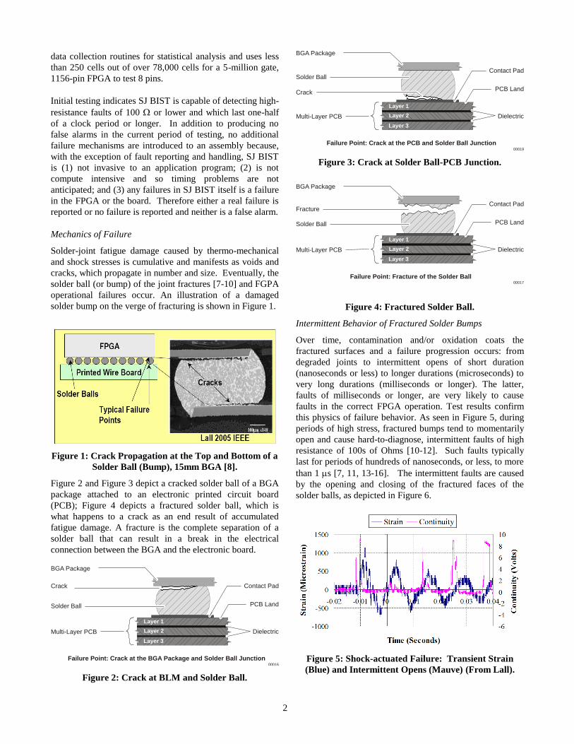
Mechanics of Failure
Solder-joint fatigue damage caused by thermo-mechanical and shock stresses is cumulative and manifests as voids and cracks, which propagate in number and size. Eventually, the solder ball (or bump) of the joint fractures [7-10] and FPGA operational failures occur. An illustration of a damaged solder bump on the verge of fracturing is shown in Figure 1.
Figure 1: Crack Propagation at the Top and Bottom of a
Solder Ball (Bump), 15mm BGA [8].
Figure 2 and Figure 3 depict a cracked solder ball of a BGA package attached to an electronic printed circuit board (PCB); Figure 4 depicts a fractured solder ball, which is what happens to a crack as an end result of accumulated fatigue damage. A fracture is the complete separation of a solder ball that can result in a break in the electrical connection between the BGA and the electronic board.
00016
BGA Package
Solder Ball
Crack
PCB Land
Contact Pad
Multi-Layer PCB Dielectric
Layer 1
Layer 2
Layer 3
Failure Point: Crack at the BGA Package and Solder Ball Junction Figure 2: Crack at BLM and Solder Ball.
00019
BGA Package
Solder Ball
CrackPCB Land
Contact Pad
Multi-Layer PCB Dielectric
Layer 1
Layer 2
Layer 3
Failure Point: Crack at the PCB and Solder Ball Junction Figure 3: Crack at Solder Ball-PCB Junction.
00017
BGA Package
Solder Ball
Fracture
PCB Land
Contact Pad
Multi-Layer PCB Dielectric
Layer 1
Layer 2
Layer 3
Failure Point: Fracture of the Solder Ball
Figure 4: Fractured Solder Ball.
Intermittent Behavior of Fractured Solder Bumps
Over time, contamination and/or oxidation coats the fractured surfaces and a failure progression occurs: from degraded joints to intermittent opens of short duration (nanoseconds or less) to longer durations (microseconds) to very long durations (milliseconds or longer). The latter, faults of milliseconds or longer, are very likely to cause faults in the correct FPGA operation. Test results confirm this physics of failure behavior. As seen in Figure 5, during periods of high stress, fractured bumps tend to momentarily open and cause hard-to-diagnose, intermittent faults of high resistance of 100s of Ohms [10-12]. Such faults typically last for periods of hundreds of nanoseconds, or less, to more than 1 s [7, 11, 13-16]. The intermittent faults are caused by the opening and closing of the fractured faces of the solder balls, as depicted in Figure 6.
Figure 5: Shock-actuated Failure: Transient Strain
(Blue) and Intermittent Opens (Mauve) (From Lall).
3
These intermittent faults increase in frequency as evidenced by a practice of logging BGA package failures only after multiple events of high-resistance: an initial event followed by some number (for example, 2 to 10) of additional events within a specified period of time, such as ten percent of the number of cycles of the initial event [14-16]. Even then, an intermittent fault in a solder-joint network might not result in an operational fault. For example, the fault might be in a ground or power connection; or it might occur during a period when the network is not being written; or it might be too short in duration to cause a signal error. In Figure 5, the duration of the fault in the 5th cycle of stress is over 3 milliseconds.
00025
Intermittent Failure caused by Fractured Solder Joint and Vibrational Stress
PCB
Solder Ball
BGA Package
Fracture
Open Circuit Closed Circuit
Vibration flexes components,intermittently opening and closingthe circuit
FPGAFPGA
Figure 6: Intermittent Open and Closed Connection.
Damage accumulates and eventually there is a catastrophic failure, such as might happen when a solder ball becomes displaced as depicted in Figure 7.
00018
BGA Package
Missing Solder Ball PCB Land
Contact Pad
Multi-Layer PCB Dielectric
Layer 1
Layer 2
Layer 3
Failure Point: Missing Solder Ball Figure 7: Displaced (Missing) Solder Ball.
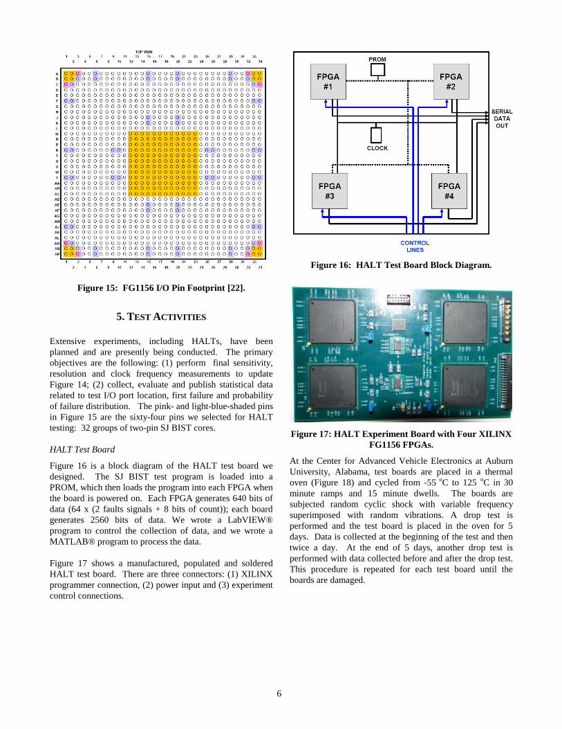
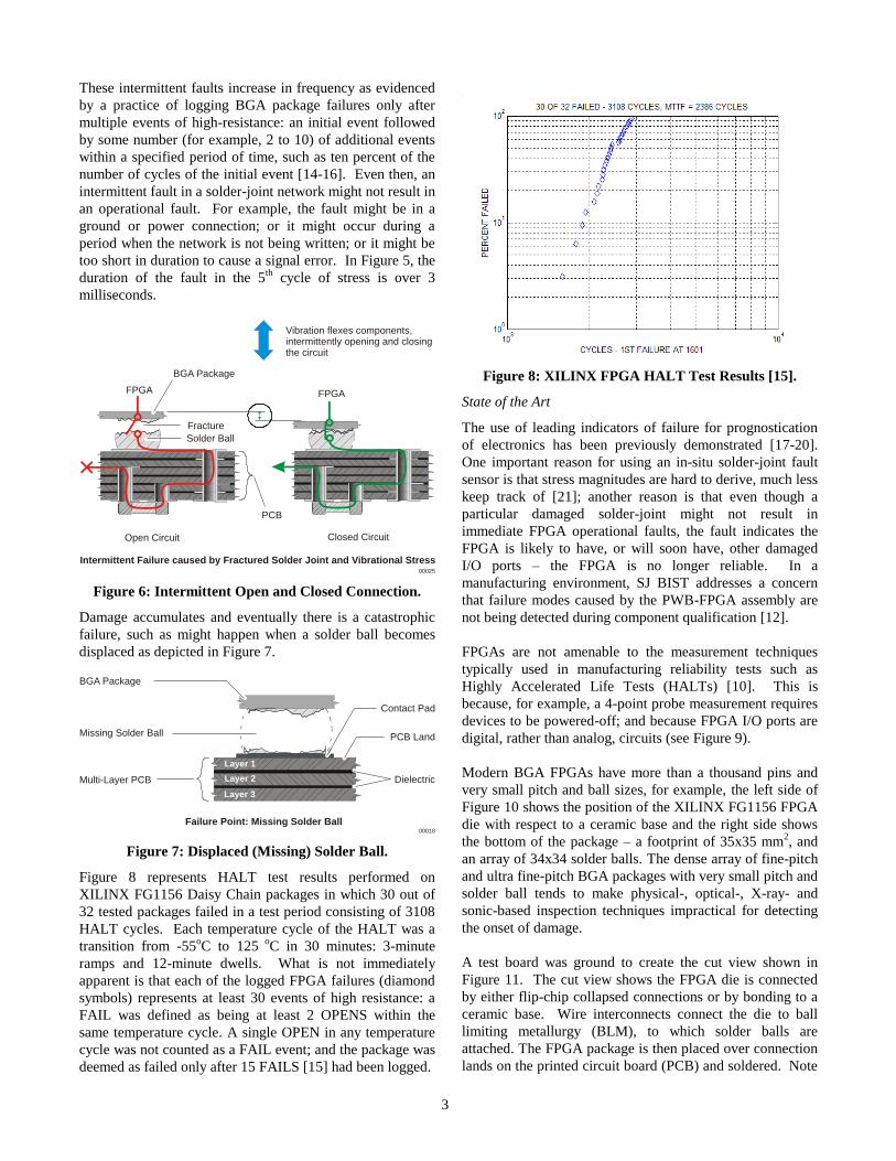
Figure 8 represents HALT test results performed on XILINX FG1156 Daisy Chain packages in which 30 out of 32 tested packages failed in a test period consisting of 3108 HALT cycles. Each temperature cycle of the HALT was a transition from -55oC to 125 oC in 30 minutes: 3-minute ramps and 12-minute dwells. What is not immediately apparent is that each of the logged FPGA failures (diamond symbols) represents at least 30 events of high resistance: a FAIL was defined as being at least 2 OPENS within the same temperature cycle. A single OPEN in any temperature cycle was not counted as a FAIL event; and the package was deemed as failed only after 15 FAILS [15] had been logged.
Figure 8: XILINX FPGA HALT Test Results [15].
State of the Art
The use of leading indicators of failure for prognostication of electronics has been previously demonstrated [17-20]. One important reason for using an in-situ solder-joint fault sensor is that stress magnitudes are hard to derive, much less keep track of [21]; another reason is that even though a particular damaged solder-joint might not result in immediate FPGA operational faults, the fault indicates the FPGA is likely to have, or will soon have, other damaged I/O ports – the FPGA is no longer reliable. In a manufacturing environment, SJ BIST addresses a concern that failure modes caused by the PWB-FPGA assembly are not being detected during component qualification [12]. FPGAs are not amenable to the measurement techniques typically used in manufacturing reliability tests such as Highly Accelerated Life Tests (HALTs) [10]. This is because, for example, a 4-point probe measurement requires devices to be powered-off; and because FPGA I/O ports are digital, rather than analog, circuits (see Figure 9). Modern BGA FPGAs have more than a thousand pins and very small pitch and ball sizes, for example, the left side of Figure 10 shows the position of the XILINX FG1156 FPGA die with respect to a ceramic base and the right side shows the bottom of the package – a footprint of 35x35 mm2, and an array of 34x34 solder balls. The dense array of fine-pitch and ultra fine-pitch BGA packages with very small pitch and solder ball tends to make physical-, optical-, X-ray- and sonic-based inspection techniques impractical for detecting the onset of damage. A test board was ground to create the cut view shown in Figure 11. The cut view shows the FPGA die is connected by either flip-chip collapsed connections or by bonding to a ceramic base. Wire interconnects connect the die to ball limiting metallurgy (BLM), to which solder balls are attached. The FPGA package is then placed over connection lands on the printed circuit board (PCB) and soldered. Note
4
the presence of voids in the two solder balls on the right-hand side of the figure.
Figure 9: FPGA Diagram, I/O Buffer [22].
Figure 10: FG1156: Size is 35x35 mm
2; Pitch: 1.0 mm.
Ball: 0.6 mm [23].
Figure 11: View Showing FPGA Die to PCB Connection.
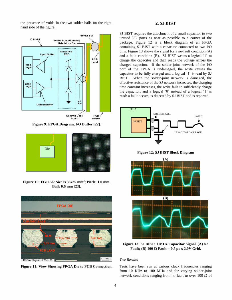
2. SJ BIST
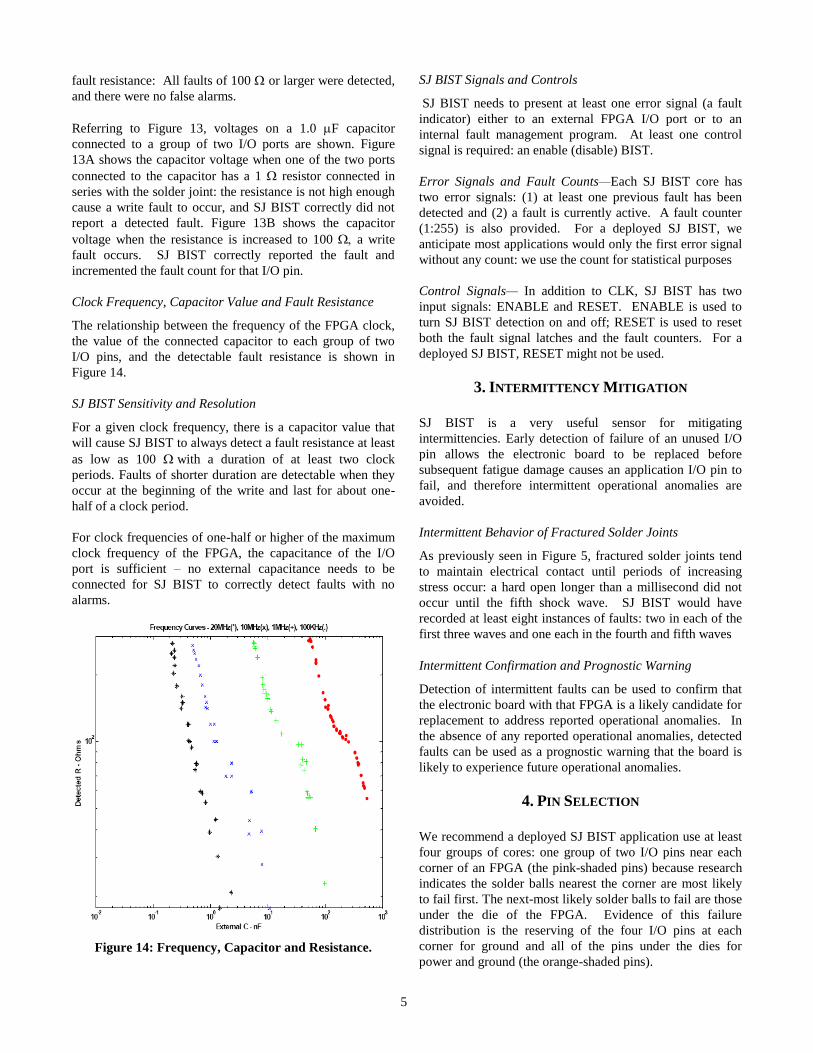
SJ BIST requires the attachment of a small capacitor to two unused I/O ports as near as possible to a corner of the package. Figure 12 is a block diagram of an FPGA containing SJ BIST with a capacitor connected to two I/O pins: Figure 13 shows the signal for a no-fault condition (A) and a fault condition (B). SJ BIST writes a logical ‘1’ to
charge the capacitor and then reads the voltage across the charged capacitor. If the solder-joint network of the I/O port of the FPGA is undamaged, the write causes the capacitor to be fully charged and a logical ‘1’ is read by SJ
BIST. When the solder-joint network is damaged, the effective resistance of the SJ network increases, the charging time constant increases, the write fails to sufficiently charge the capacitor, and a logical ‘0’ instead of a logical ‘1’ is
read: a fault occurs, is detected by SJ BIST and is reported.
Figure 12: SJ BIST Block Diagram
(A)
(B)
Figure 13: SJ BIST: 1 MHz Capacitor Signal. (A) No
Fault; (B) 100 Fault 0.5 s x 2.0V Grid.
Test Results
Tests have been run at various clock frequencies ranging from 10 KHz to 100 MHz and for varying solder-joint network conditions ranging from no fault to over 100 of
FPGA
SJ BIST
SOLDER BALL
CAPACITOR VOLTAGE
FAULT
Die