Embed Size (px)
Citation preview
Chapter No 5
Basic Computer OrganizationAnd
Design

Figure 5-1 Stored Program Organization
Address
11 01215
Binary Operand
Instruction(Program)
Opcode
Memory4096*16
Operand(Data)
Processor Register(Ac)
015Instruction format
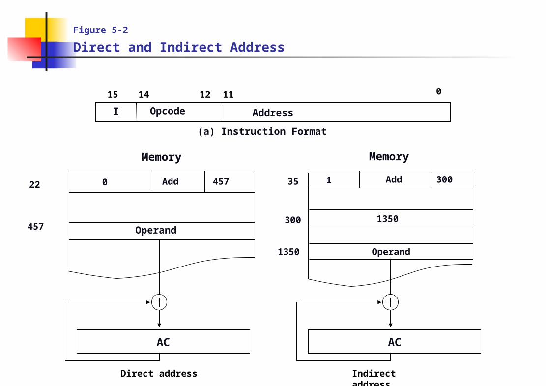
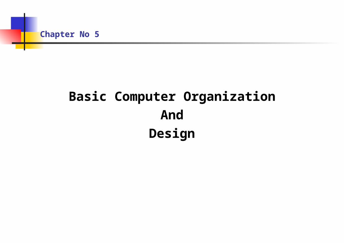
Figure 5-2 Direct and Indirect Address
AddressOpcodeI
011121415
(a) Instruction Format
Operand457
457
Memory
Add022
AC
1350300
35 1
Operand1350
Memory
300Add
AC
Direct address Indirect address

Table 5-1 List Of Register
Registersymbol
Bits Register name Function
DR
AR
AC
IR
PC
TR
16
12
16
16
12
16
Data Register
Address Register
Accumulator
Instruction Register
Program Register
Hold Memory Operand
Address to Me
Processor Register
Hold Instruction Code
Address of InsTemporary Data
Inpr 8 Input Reg Input Character
Outr 8 Output Register Hold output Character
Temporary Register

Figure 5-3 Basic Computer Register and memory.
PC
011
Memory4096 word
16 bits per word
IR
015
INPR
07
AR
011
TR
015
OUTR
07
DR
015
AC
015
Figure 5-4 Computer Register Connect to Common Bus
Memory unit4096 x 16
AR
BusS2S1S0
PC
DR
AC
Adder
And
logic
INPR
IR
TR
OUTR
Address7
1
2
3
4
5
6
E
16-bit common bus
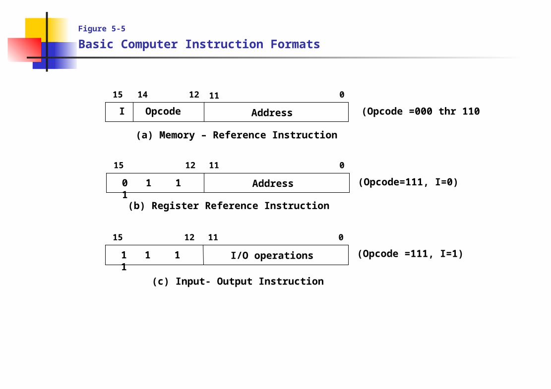
Figure 5-5 Basic Computer Instruction Formats
(Opcode =000 thr 110AddressOpcodeI
011121415
(a) Memory – Reference Instruction
(b) Register Reference Instruction
(c) Input- Output Instruction
(Opcode=111, I=0)
(Opcode =111, I=1)
Address0 1 1 1
0111215
I/O operations1 1 1 1
0111215
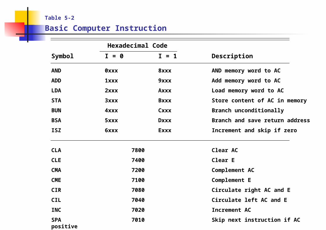
Table 5-2 Basic Computer Instruction
Hexadecimal Code
Symbol I = 0 I = 1 Description
AND 0xxx 8xxx AND memory word to AC
ADD 1xxx 9xxx Add memory word to AC
LDA 2xxx Axxx Load memory word to AC
STA 3xxx Bxxx Store content of AC in memory
BUN 4xxx Cxxx Branch unconditionally
BSA 5xxx Dxxx Branch and save return address
ISZ 6xxx Exxx Increment and skip if zero
CLA 7800 Clear AC
CLE 7400 Clear E
CMA 7200 Complement AC
CME 7100 Complement E
CIR 7080 Circulate right AC and E
CIL 7040 Circulate left AC and E
INC 7020 Increment AC
SPA 7010 Skip next instruction if AC positive
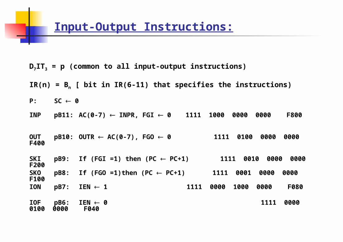
Input-Output Instructions:
D7IT3 = p (common to all input-output instructions)
IR(n) = Bn [ bit in IR(6-11) that specifies the instructions)
P: SC 0
INP pB11: AC(0-7) INPR, FGI 0 1111 1000 0000 0000 F800
OUT pB10: OUTR AC(0-7), FGO 0 1111 0100 0000 0000 F400
SKI pB9: If (FGI =1) then (PC PC+1) 1111 0010 0000 0000 F200
SKO pB8: If (FGO =1)then (PC PC+1) 1111 0001 0000 0000 F100
ION pB7: IEN 1 1111 0000 1000 0000 F080
IOF pB6: IEN 0 1111 0000 0100 0000 F040
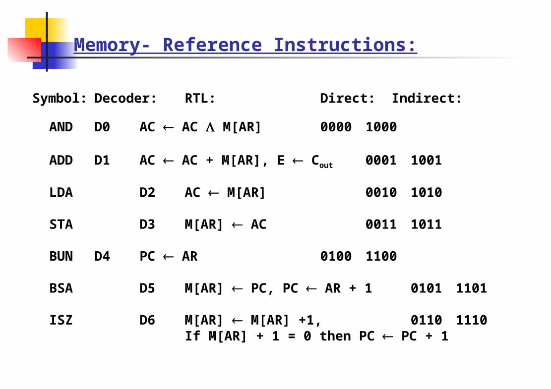
Memory- Reference Instructions:
Symbol:Decoder: RTL: Direct: Indirect:
AND D0 AC AC M[AR] 0000 1000
ADD D1 AC AC + M[AR], E Cout 0001 1001
LDA D2 AC M[AR] 0010 1010
STA D3 M[AR] AC 0011 1011
BUN D4 PC AR 0100 1100
BSA D5 M[AR] PC, PC AR + 1 0101 1101
ISZ D6 M[AR] M[AR] +1, 0110 1110If M[AR] + 1 = 0 then PC PC + 1
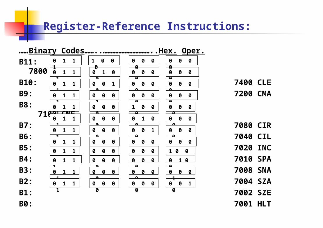
Register-Reference Instructions:
…… Binary Codes……..…………………………..Hex. Oper. B11: 7800 CLAB10: 7400 CLEB9: 7200 CMAB8: 7100 CMEB7: 7080 CIR B6: 7040 CILB5: 7020 INCB4: 7010 SPAB3: 7008 SNAB2: 7004 SZAB1: 7002 SZEB0: 7001 HLT
0 1 1 1
0 1 0 0
0 0 0 0
0 0 0 0
0 1 1 1
0 0 0 00 0 0 0
0 0 1 0
0 1 1 1
0 0 0 1
0 0 0 0
0 0 0 0
0 1 1 1
0 0 0 0
1 0 0 0
0 0 0 0
0 1 1 1
0 0 0 0
0 0 0 0
0 1 0 0
0 1 1 1
1 0 0 0
0 0 0 0
0 0 0 0
0 1 1 1
0 0 0 0
0 0 1 0
0 0 0 0
0 1 1 1
0 0 0 0
0 0 0 1
0 0 0 00 1 1
10 0 0 0
0 0 0 0
1 0 0 00 1 1
10 0 0 0
0 0 0 0
0 1 0 0
0 1 1 1
0 0 0 0
0 0 0 0
0 0 1 0
0 1 1 1
0 0 0 0
0 0 0 0
0 0 0 1

Table 5-2 Basic Computer Instruction:
Hexadecimal Code
Symbol I = 0 I = 1 Description
SNA 7008 Skip next instruction if AC negative
SZA 7004 Skip next instruction if AC zero
SZE 7002 Skip next instruction if E zero
HLT 7001 Halt computer
INP F800 Input character to AC
OUT F400 Output character from AC
SKI F200 Skip on input flag
SKO F100 Skip on output flag
ION F080 Interrupt on
IOF F040 Interrupt on
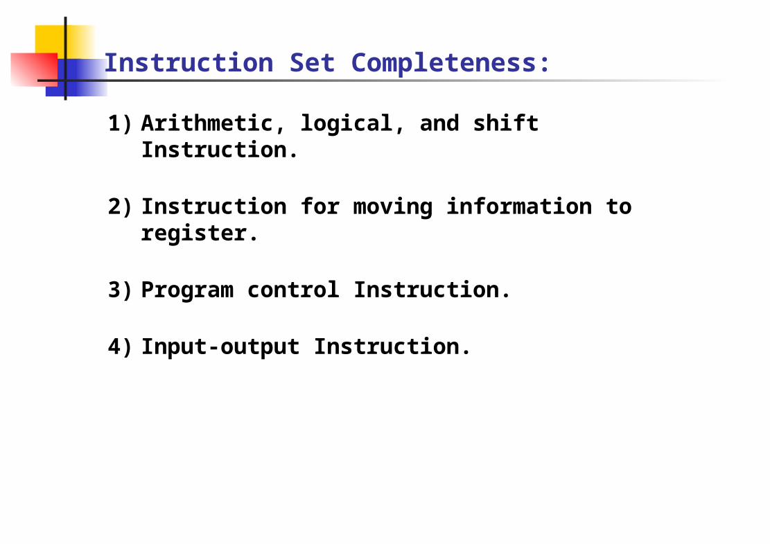
Instruction Set Completeness:
1) Arithmetic, logical, and shift Instruction.
2) Instruction for moving information to register.
3) Program control Instruction.
4) Input-output Instruction.
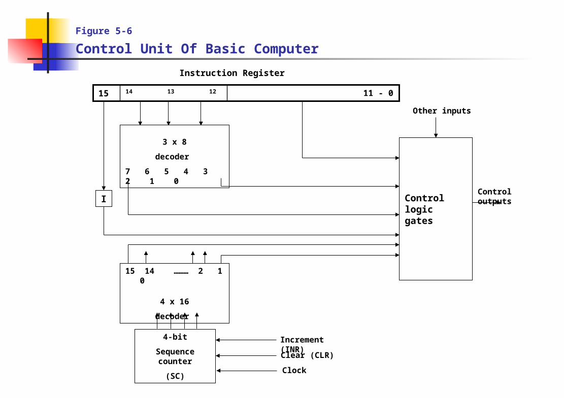
Figure 5-6 Control Unit Of Basic Computer
Instruction Register
11 - 014 13 1215
3 x 8
decoder
7 6 5 4 3 2 1 0
Control logic gates
Other inputs
I
15 14 ……… 2 1 0
4 x 16
decoder
4-bit
Sequence counter
(SC)
Control outputs
Increment (INR)Clear (CLR)
Clock
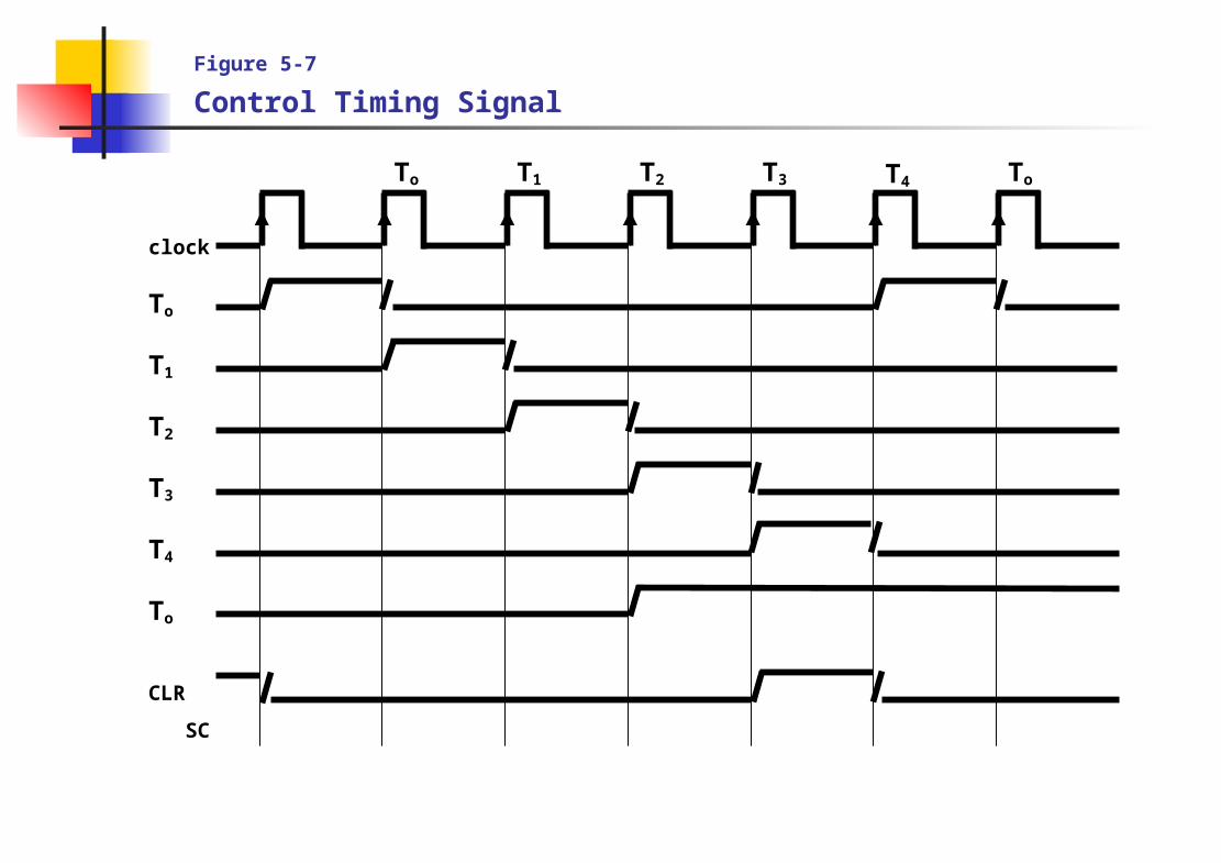
Figure 5-7 Control Timing Signal
To T1 T2 T3 T4 To
clock
To
T1
T2
T3
T4
To
CLR
SC
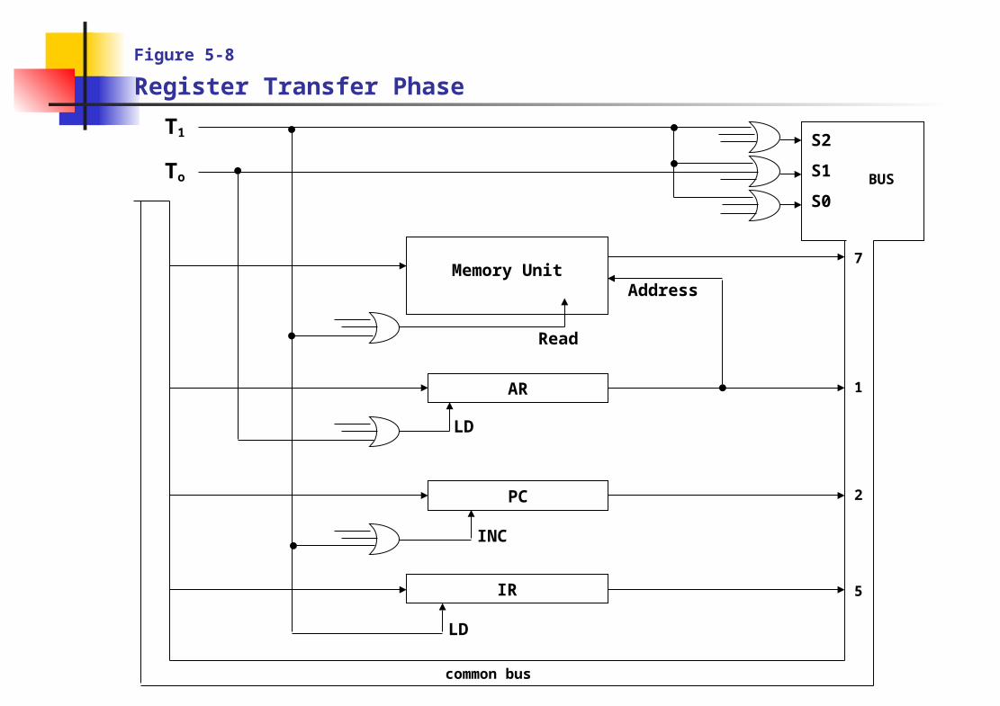
Figure 5-8 Register Transfer Phase
S2
S1
S0
Memory Unit
AR
PC
IR
To
T1
Read
LD
INC
LD
Address
7
1
2
5
common bus
BUS
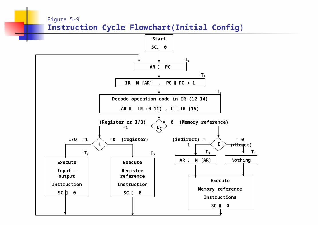
Figure 5-9
Instruction Cycle Flowchart(Initial Config)Start
SC 0
AR PC
IR M [AR] , PC PC + 1
Decode operation code in IR (12-14)
AR IR (0-11) , I IR (15)
D7
I I
Execute
Register reference
Instruction
SC 0
Execute
Input - output
Instruction
SC 0
AR M [AR] Nothing
Execute
Memory reference
Instructions
SC 0
(Register or I/O) =1 = 0 (Memory reference)
I/O =1 =0 (register) (indirect) = 1 = 0 (direct)
T0
T1
T2
T3 T3T3 T3
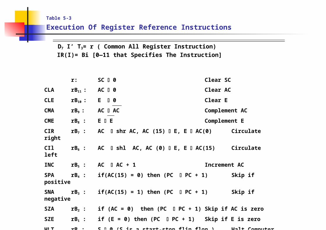
Table 5-3 Execution Of Register Reference Instructions
D7 I’ T3= r ( Common All Register Instruction)IR(I)= Bi [0—11 that Specifies The Instruction]
r: SC 0 Clear SC
CLA rB11 : AC 0 Clear AC
CLE rB10 : E 0 Clear E
CMA rB9 : AC AC Complement AC
CME rB8 : E E Complement E
CIR rB7 : AC shr AC, AC (15) E, E AC(0) Circulate right
CIl rB6 : AC shl AC, AC (0) E, E AC(15) Circulate left
INC rB5 : AC AC + 1 Increment AC
SPA rB4 : if(AC(15) = 0) then (PC PC + 1) Skip if positive
SNA rB3 : if(AC(15) = 1) then (PC PC + 1) Skip if negative
SZA rB2 : if (AC = 0) then (PC PC + 1) Skip if AC is zero
SZE rB1 : if (E = 0) then (PC PC + 1) Skip if E is zero
HLT rB0 : S 0 (S is a start-stop flip flop ) Halt Computer
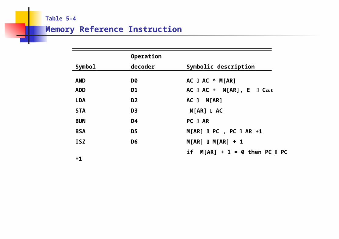
Table 5-4 Memory Reference Instruction
Operation
Symbol decoder Symbolic description
AND D0 AC AC ^ M[AR]
ADD D1 AC AC + M[AR], E Ccut
LDA D2 AC M[AR]
STA D3 M[AR] AC
BUN D4 PC AR
BSA D5 M[AR] PC , PC AR +1
ISZ D6 M[AR] M[AR] + 1
if M[AR] + 1 = 0 then PC PC +1
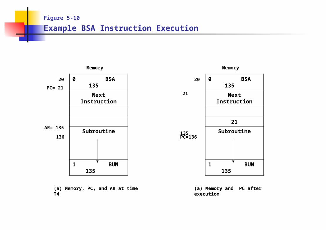
Figure 5-10 Example BSA Instruction Execution
0 BSA 135
Next Instruction
Subroutine
1 BUN 135
Memory
20
PC= 21
AR= 135
136
(a) Memory, PC, and AR at time T4
0 BSA 135
Next Instruction
21
Subroutine
1 BUN 135
Memory
20
21
135
PC=136
(a) Memory and PC after execution
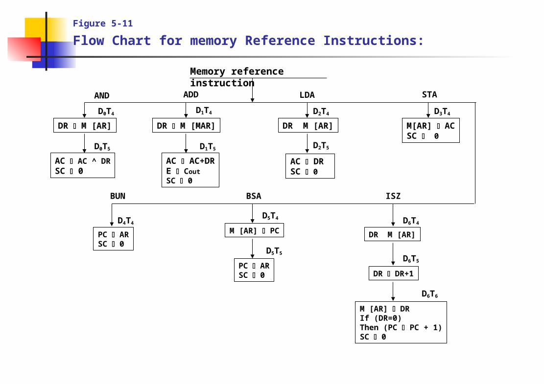
Figure 5-11 Flow Chart for memory Reference Instructions:
Memory reference instruction
PC ARSC 0
M [AR] PC DR M [AR]
DR M [AR] DR M [MAR] DR M [AR] M[AR] ACSC 0
AC AC ^ DRSC 0
AC AC+DRE Cout
SC 0
AC DRSC 0
AND ADD LDA STA
D0T4 D1T4 D2T4 D3T4
D0T5 D1T5 D2T5
BUN BSA ISZ
D4T4D5T4 D6T4
PC ARSC 0
D5T5
DR DR+1
D6T5
M [AR] DRIf (DR=0)Then (PC PC + 1)SC 0
D6T6
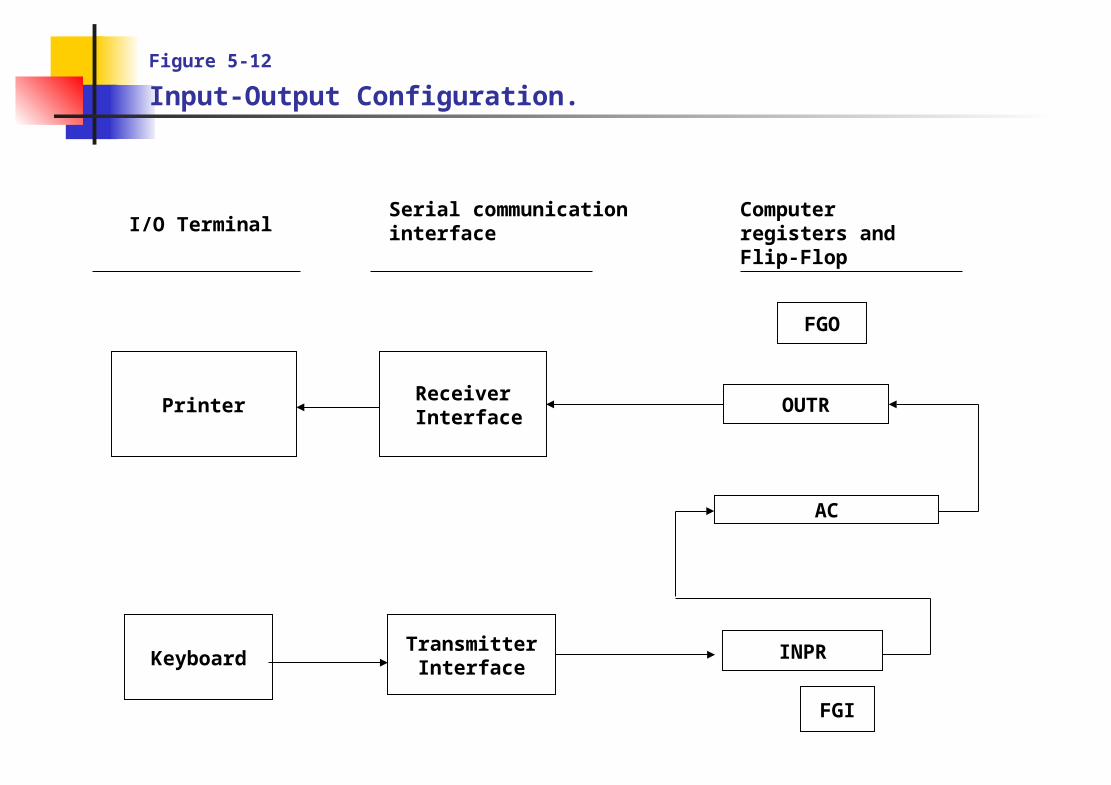
Figure 5-12 Input-Output Configuration.
I/O TerminalSerial communicationinterface
Computer registers and Flip-Flop
FGO
PrinterReceiver Interface
OUTR
AC
INPRTransmitterInterface
FGI
Keyboard
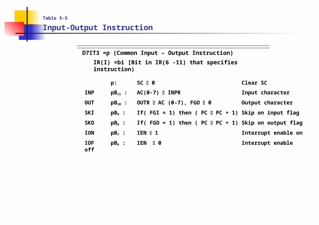
Table 5-5 Input-Output Instruction
D7IT3 =p (Common Input – Output Instruction)
IR(I) =bi [Bit in IR(6 -11) that specifies instruction)
p: SC 0 Clear SC
INP pB11 : AC(0-7) INPR Input character
OUT pB10 : OUTR AC (0-7), FGO 0 Output character
SKI pB9 : If( FGI = 1) then ( PC PC + 1) Skip on input flag
SKO pB8 : If( FGO = 1) then ( PC PC + 1) Skip on output flag
ION pB7 : IEN 1 Interrupt enable on
IOF pB6 : IEN 0 Interrupt enable off
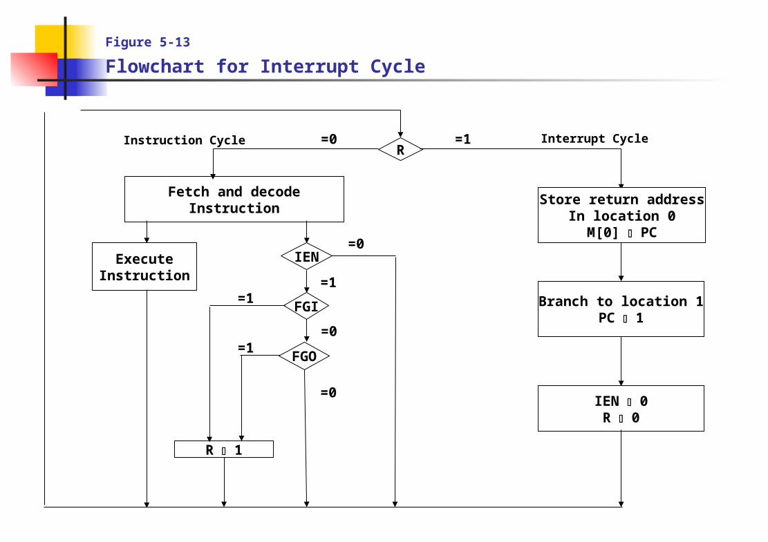
Figure 5-13 Flowchart for Interrupt Cycle
R=0 =1Instruction Cycle Interrupt Cycle
Fetch and decodeInstruction
ExecuteInstruction
IEN=0
FGI
=1
R 1
FGO
=0
Store return addressIn location 0
M[0] PC
Branch to location 1PC 1
IEN 0R 0
=0
=1
=1
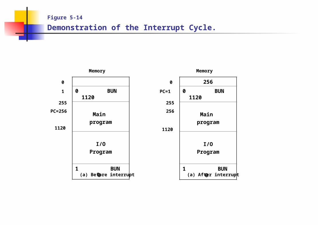
Figure 5-14 Demonstration of the Interrupt Cycle.
0 BUN 1120
Main program
I/OProgram
1 BUN 0
Memory
0
1
1120
(a) Before interrupt
255
PC=256
256
0 BUN 1120
Main program
I/OProgram
1 BUN 0
Memory
0
PC=1
1120
(a) After interrupt
255
256
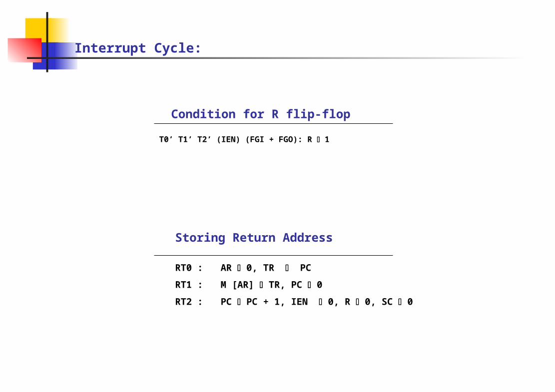
Interrupt Cycle:
RT0 : AR 0, TR PC
RT1 : M [AR] TR, PC 0
RT2 : PC PC + 1, IEN 0, R 0, SC 0
Storing Return Address
Condition for R flip-flop
T0’ T1’ T2’ (IEN) (FGI + FGO): R 1
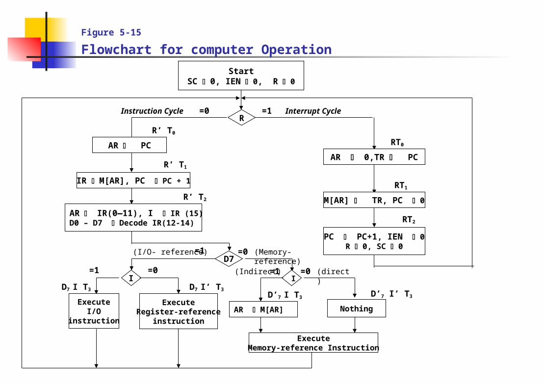
Figure 5-15 Flowchart for computer Operation
StartSC 0, IEN 0, R 0
R
AR PC
R’ T0
IR M[AR], PC PC + 1
AR 0,TR PCR’ T1
RT0
M[AR] TR, PC 0
RT1
PC PC+1, IEN 0R 0, SC 0
RT2
AR IR(0—11), I IR (15)D0 – D7 Decode IR(12-14)
D7=0
I=0=1
AR M[AR] Nothing
D’7 I’ T3D’7 I T3
ExecuteMemory-reference Instruction
=1
I
ExecuteRegister-reference
instruction
ExecuteI/O
instruction
=0=1
R’ T2
Interrupt Cycle
=1
=0Instruction Cycle
(direct)(Indirect)
(Memory-reference)
(I/O- reference)
D7 I’ T3D7 I T3
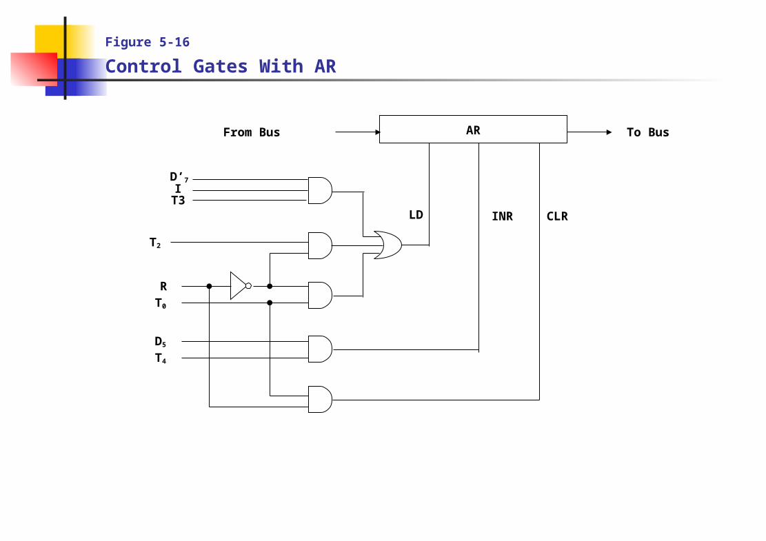
Figure 5-16 Control Gates With AR
ARFrom Bus To Bus
LD INR CLR
D’7
IT3
T2
RT0
D5
T4
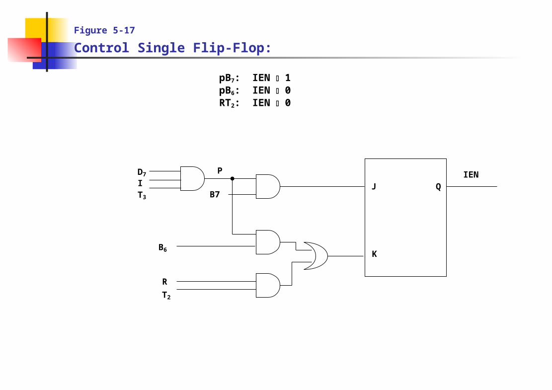
Figure 5-17 Control Single Flip-Flop:
pB7: IEN 1pB6: IEN 0RT2: IEN 0
IENJ
K
D7
IT3
P
R
T2
B6
B7Q
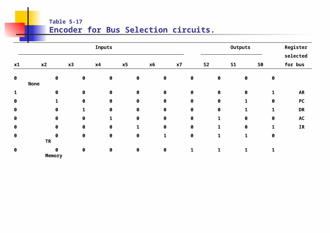
Table 5-17
Encoder for Bus Selection circuits.
Inputs Outputs Register
selected
x1 x2 x3 x4 x5 x6 x7 S2 S1 S0 for bus
0 0 0 0 0 0 0 0 0 0None
1 0 0 0 0 0 0 0 0 1 AR
0 1 0 0 0 0 0 0 1 0 PC
0 0 1 0 0 0 0 0 1 1 DR
0 0 0 1 0 0 0 1 0 0 AC
0 0 0 0 1 0 0 1 0 1 IR
0 0 0 0 0 1 0 1 1 0 TR
0 0 0 0 0 0 1 1 1 1 Memory
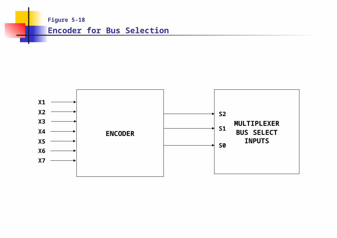
Figure 5-18 Encoder for Bus Selection
ENCODER
MULTIPLEXERBUS SELECT
INPUTS
S2
S1
S0
X1
X2
X3
X4
X5
X6
X7
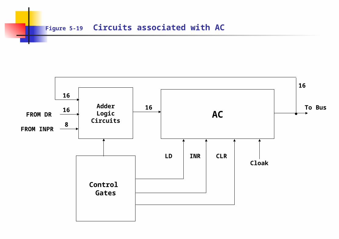
Figure 5-19 Circuits associated with AC
ACTo BusAdder
LogicCircuits
Control Gates
16
16
16
FROM INPR
FROM DR
LD INR CLRCloak
16
8
Figure 5-20 Gates controlling the Ld,INR, and CLR OF AC
AC To BUSAdder logic
LD INR CLR
AND
ADD
DR
INPR
COM
SHR
SHL
INC
CLR
r
B7
B6
B5
B11
pB11
D2
T5
D1
D0T5
B9
16
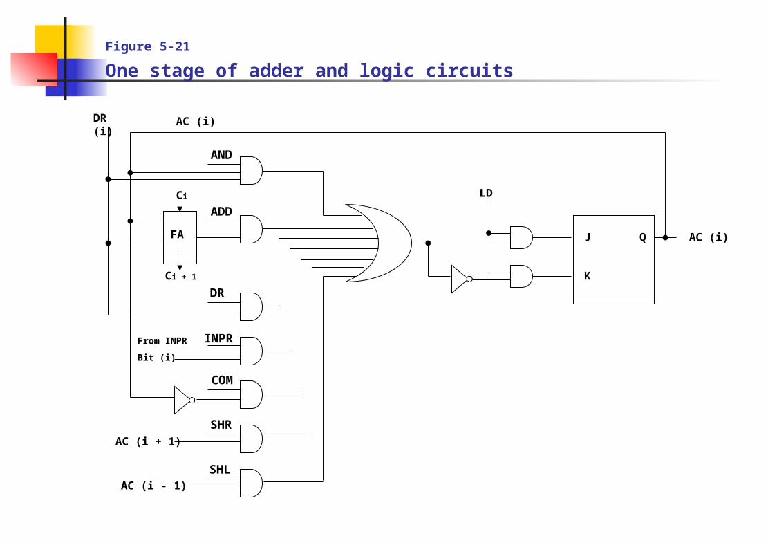
Figure 5-21 One stage of adder and logic circuits
J
K
Q AC (i)
LD
FA
ADDCi
AND
Ci + 1
DR
INPR
COM
SHR
SHL
From INPR
Bit (i)
AC (i + 1)
AC (i - 1)
DR (i)
AC (i)