Embed Size (px)
DESCRIPTION
FPCCD Vertex Detector for ILC. 2007.2.6 @9 th -ACFA, Beijing Y. Sugimoto KEK. Challenge of ILC VTX. To achieve the performance goal of s IP = 5 10/( p b sin 3/2 q ) m m; Material budget should be small: < 0.1% X 0 / layer 1 st layer should be put as close to the IP as possible. - PowerPoint PPT Presentation
Citation preview
FPCCD Vertex Detector for ILC
2007.2.6
@9th-ACFA, Beijing
Y. Sugimoto
KEK
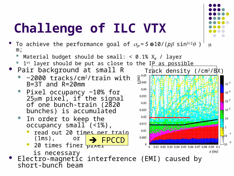
Challenge of ILC VTX
Pair background at small R ~2000 tracks/cm2/train with B=3T
and R=20mm Pixel occupancy ~10% for 25m
pixel, if the signal of one bunch-train (2820 bunches) is accumulated
In order to keep the occupancy small (<1%), read out 20 times per train (1ms),
or 20 times finer pixel
is necessary
Track density (/cm2/BX)
To achieve the performance goal of IP = 5 10/(psin3/2) m; Material budget should be small: < 0.1% X0 / layer 1st layer should be put as close to the IP as possible
FPCCD
Electro-magnetic interference (EMI) caused by short-bunch beam
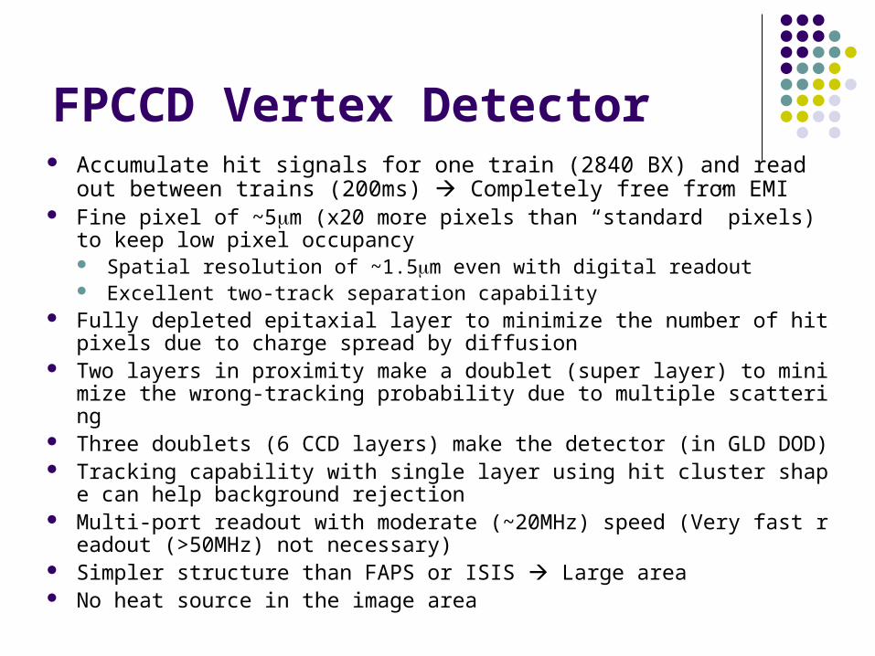
FPCCD Vertex Detector Accumulate hit signals for one train (2840 BX) and read out between
trains (200ms) Completely free from EMI Fine pixel of ~5m (x20 more pixels than “standard” pixels) to keep low pi
xel occupancy Spatial resolution of ~1.5m even with digital readout Excellent two-track separation capability
Fully depleted epitaxial layer to minimize the number of hit pixels due to charge spread by diffusion
Two layers in proximity make a doublet (super layer) to minimize the wrong-tracking probability due to multiple scattering
Three doublets (6 CCD layers) make the detector (in GLD DOD) Tracking capability with single layer using hit cluster shape can help back
ground rejection Multi-port readout with moderate (~20MHz) speed (Very fast readout (>5
0MHz) not necessary) Simpler structure than FAPS or ISIS Large area No heat source in the image area
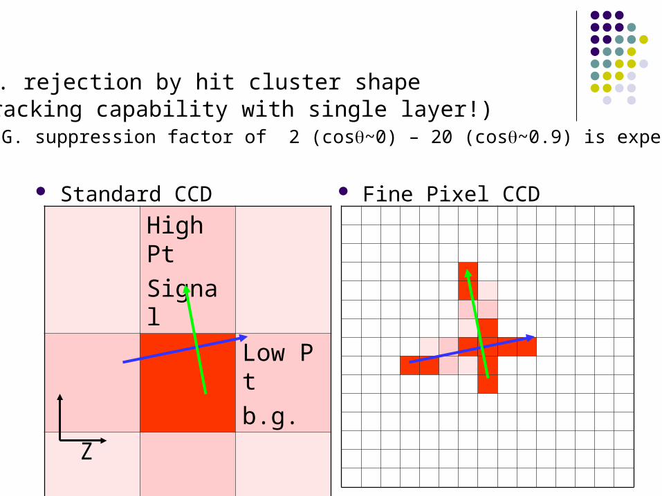
Standard CCD Fine Pixel CCD
High Pt
Signal
Low Pt
b.g.
Z
B.G. rejection by hit cluster shape (tracking capability with single layer!) B.G. suppression factor of 2 (cos~0) – 20 (cos~0.9) is expected
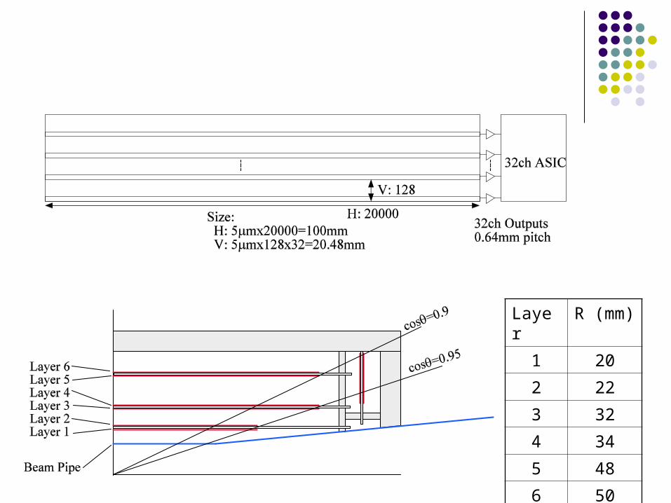
Layer R (mm)
1 20
2 22
3 32
4 34
5 48
6 50
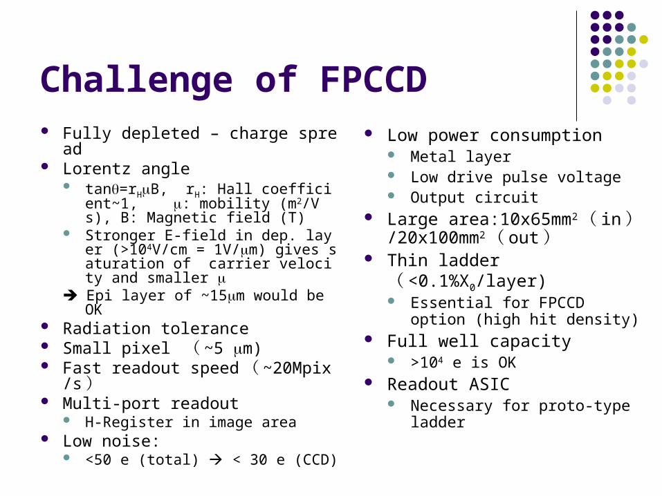
Challenge of FPCCD Fully depleted – charge spread Lorentz angle
tan=rHB, rH: Hall coefficient~1, : mobility (m2/Vs), B: Magnetic field (T)
Stronger E-field in dep. layer (>104V/cm = 1V/m) gives saturation of carrier velocity and smaller
Epi layer of ~15m would be OK Radiation tolerance Small pixel ( ~5 m) Fast readout speed ( ~20Mpix/
s ) Multi-port readout
H-Register in image area Low noise:
<50 e (total) < 30 e (CCD)
Low power consumption Metal layer Low drive pulse voltage Output circuit
Large area:10x65mm2 ( in ) /20x100mm2 ( out )
Thin ladder ( <0.1%X0/layer) Essential for FPCCD option
(high hit density) Full well capacity
>104 e is OK Readout ASIC
Necessary for proto-type ladder
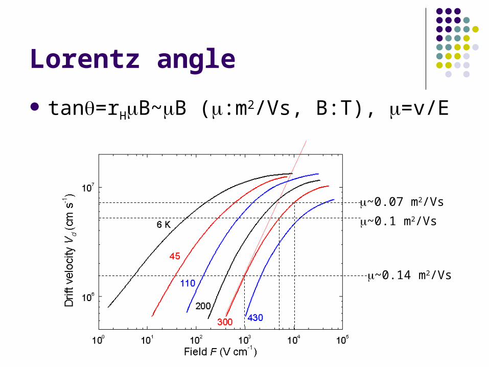
Lorentz angle
tan=rHB~B (:m2/Vs, B:T), =v/E
~0.1 m2/Vs
~0.07 m2/Vs
~0.14 m2/Vs
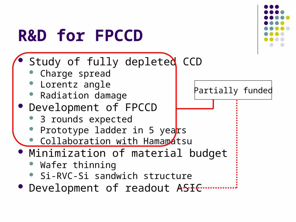
R&D for FPCCD Study of fully depleted CCD
Charge spread Lorentz angle Radiation damage
Development of FPCCD 3 rounds expected Prototype ladder in 5 years Collaboration with Hamamatsu
Minimization of material budget Wafer thinning Si-RVC-Si sandwich structure
Development of readout ASIC
Partially funded
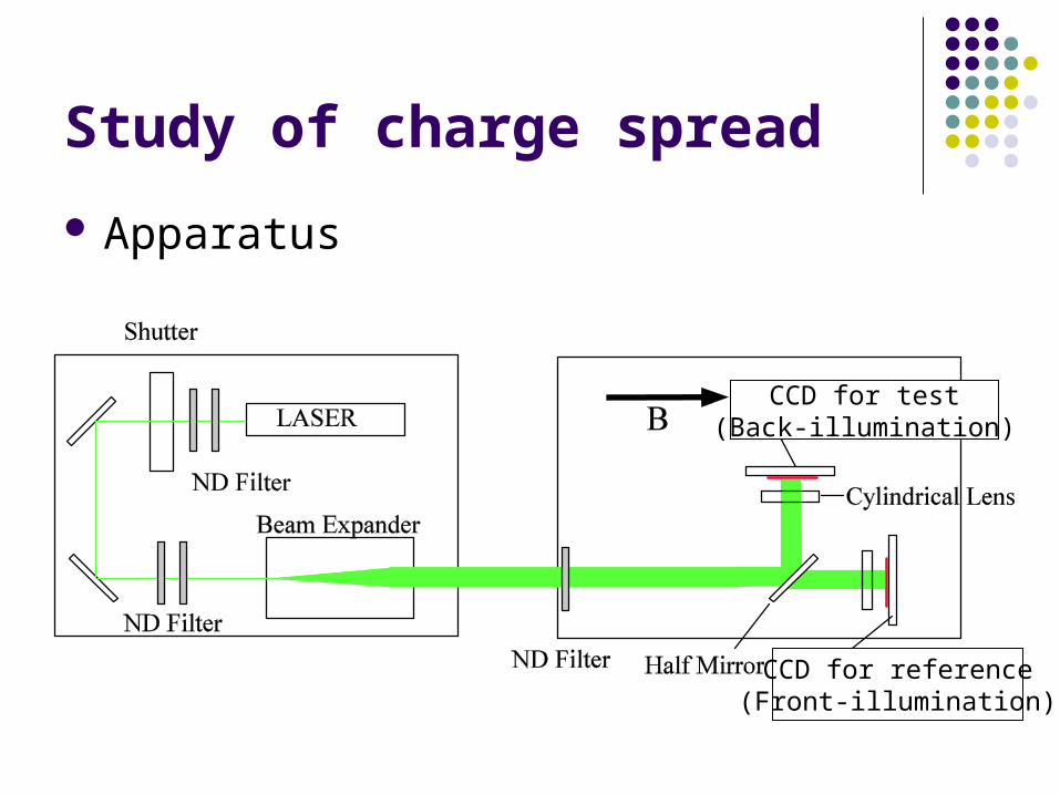
Study of charge spread
Apparatus
CCD for reference(Front-illumination)
CCD for test(Back-illumination)
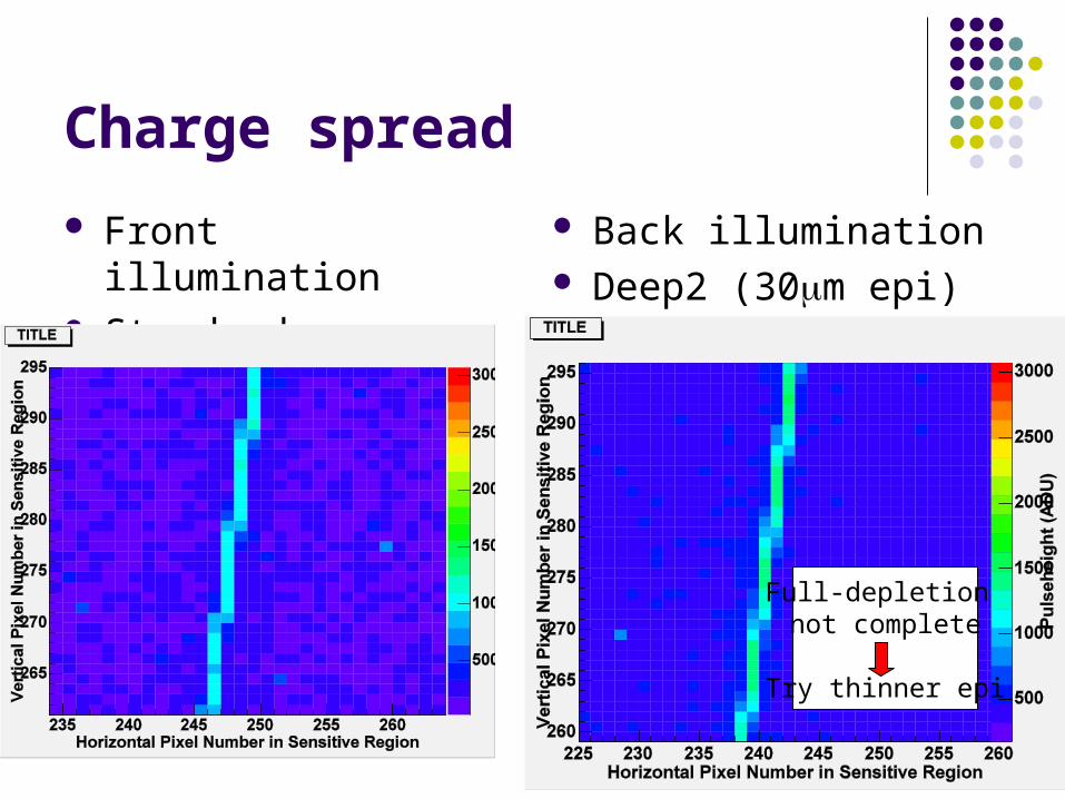
Charge spread
Front illumination Standard
Back illumination Deep2 (30m epi)
Full-depletion not complete
Try thinner epi
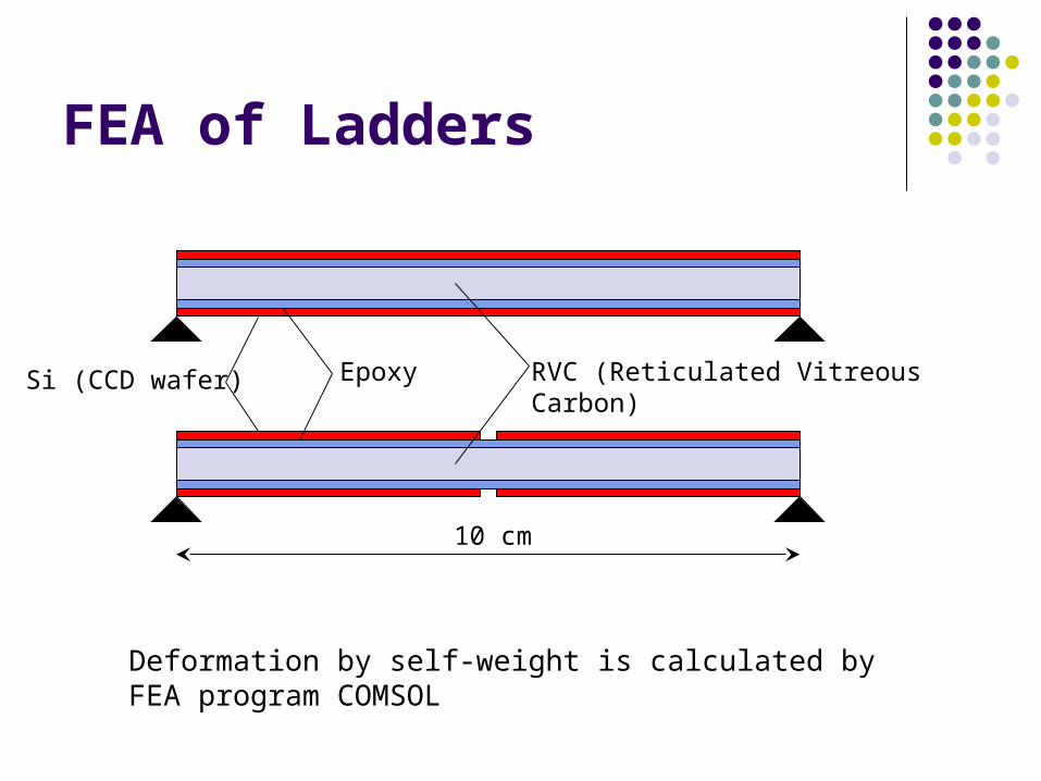
FEA of Ladders
Si (CCD wafer) RVC (Reticulated Vitreous Carbon)
10 cm
Epoxy
Deformation by self-weight is calculated byFEA program COMSOL
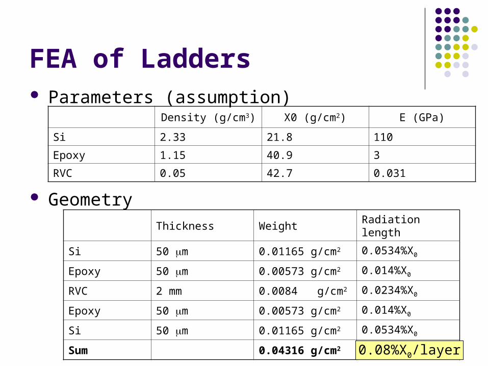
FEA of Ladders Parameters (assumption)
Geometry
Density (g/cm3) X0 (g/cm2) E (GPa)
Si 2.33 21.8 110
Epoxy 1.15 40.9 3
RVC 0.05 42.7 0.031
Thickness Weight Radiation length
Si 50 m 0.01165 g/cm2 0.0534%X0
Epoxy 50 m 0.00573 g/cm2 0.014%X0
RVC 2 mm 0.0084 g/cm2 0.0234%X0
Epoxy 50 m 0.00573 g/cm2 0.014%X0
Si 50 m 0.01165 g/cm2 0.0534%X0
Sum 0.04316 g/cm2 0.1582%X0
0.08%X0/layer
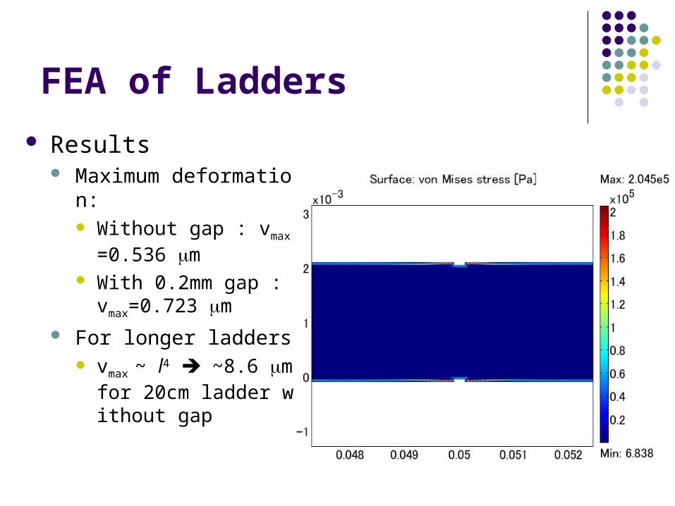
FEA of Ladders
Results Maximum deformation:
Without gap : vmax=0.536 m
With 0.2mm gap : vmax
=0.723 m For longer ladders
vmax ~ l4 ~8.6 m for 20cm ladder without gap
Summary We have started R&D of FPCCD for ILC vertex detector Study of fully depleted CCD is on going in FY2006, and will be continue
d to FY2007 CCD sample with 30m epi seems not fully depleted We will try to measure 15m epi sample soon Lorentz angle measurement and radiation damage test are planned
Finite element analysis was done for a ladder of Si-RVC-Si sandwich structure 0.08% radiation length per layer with [50m Si]x2 + [50m epoxi]x2 + [2mm
RVC] Deformation by self weight is less than 10m for 20cm long ladder
The 1st test sample of FPCCD is expected to be made by Hamamatsu in FY2007
We wish to construct and test prototype ladders of FPCCD in 4years, but the budget (for r.o. ASIC and support structure) is not enough to complete that goal