Embed Size (px)
Citation preview
Fermilab, 17.07.2006 LABSilizium Labor Bonn
SIMarcel Trimpl, University of Bonn- 1 -
DEPFET Seminar Fermilab, July 2006
M.Trimpl
DEPFET – collaboration:
MPI/MPE Munich
L.Andricek, P.Lechner, H.G. Moser, R.H.Richter, L.Strüder, G.Lutz, J.Treis
U Mannheim
P.Fischer, F.Giesen, C.Kreidel, I.Peric
U Bonn
M.Koch, R.Kohrs, H.Krüger, P.Lodomez, L.Reuen, C.Sandow, M.Trimpl, E.v.Törne, J.J.Velthuis, N.Wermes
U Prague
Z.Doležal, P Kodyš, D.Scheirich
U Aachen
L.Feld, W.Karpinski, K.Klein
DEPFET pixels for the ILC vertex detector
Fermilab, 17.07.2006 LABSilizium Labor Bonn
SIMarcel Trimpl, University of Bonn- 2 -
• Introduction: ILC project, vtx-d and requirements
• DEPFET technology:principle, present production and thinning approach
• Sensor characterization: clear, rad. tolerance
• Overview: ILC DEPFET-System
• R/O - electronics (CURO- FE):
architecture, circuit realization and results
• Results with present system (lab, beam test)
• Summary and Outlook
outline
Fermilab, 17.07.2006 LABSilizium Labor Bonn
SIMarcel Trimpl, University of Bonn- 3 -
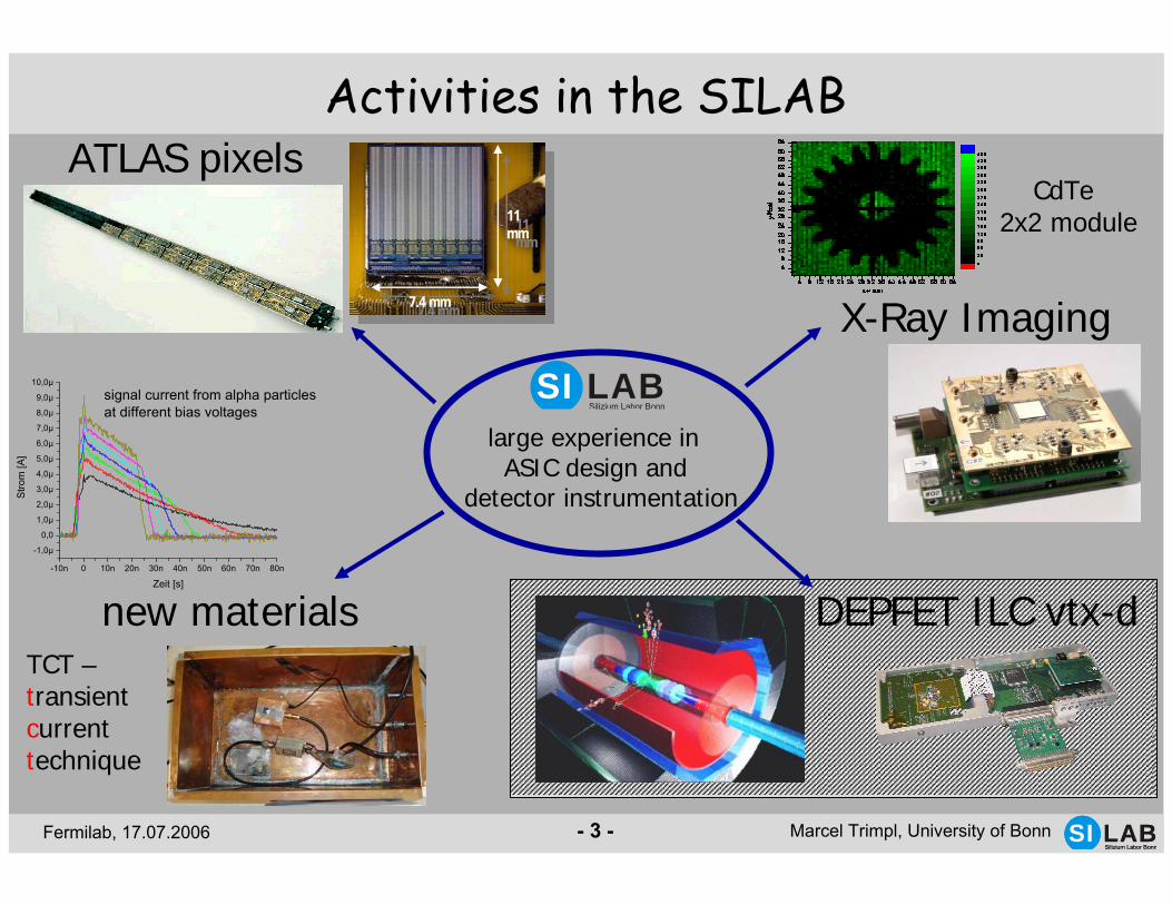
Activities in the SILAB
-10n 0 10n 20n 30n 40n 50n 60n 70n 80n
-1,0µ
0,0
1,0µ
2,0µ
3,0µ
4,0µ
5,0µ
6,0µ
7,0µ
8,0µ
9,0µ
10,0µ
signal current from alpha particlesat different bias voltages
Stro
m [A
]
Zeit [s]
large experience in ASIC design and
detector instrumentation
11mm
11mm
7.4 mm7.4 mm
ATLAS pixels
new materials
X-Ray Imaging
LABSilizium Labor Bonn
SI
LABSilizium Labor Bonn
SI
DEPFET ILC vtx-d
CdTe2x2 module
TCT –transient current technique
Fermilab, 17.07.2006 LABSilizium Labor Bonn
SIMarcel Trimpl, University of Bonn- 4 -
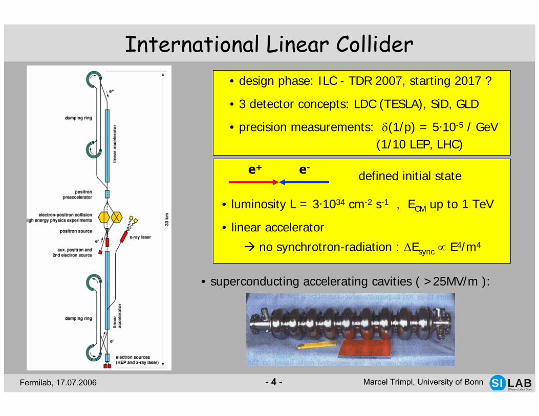
• linear accelerator
no synchrotron-radiation : ∆Esync ∝ E4/m4
• luminosity L = 3·1034 cm-2 s-1 , ECM up to 1 TeV
International Linear Collider
• superconducting accelerating cavities ( >25MV/m ):
• design phase: ILC - TDR 2007, starting 2017 ?
• precision measurements: δ(1/p) = 5·10-5 / GeV(1/10 LEP, LHC)
e+ e-defined initial state
• 3 detector concepts: LDC (TESLA), SiD, GLD
Fermilab, 17.07.2006 LABSilizium Labor Bonn
SIMarcel Trimpl, University of Bonn- 5 -
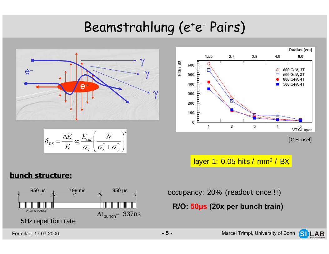
950 µs 199 ms 950 µs
2820 bunchesR/O: 50µs (20x per bunch train)
Beamstrahlung (e+e- Pairs)
bunch structure:
∆tbunch= 337ns
layer 1: 0.05 hits / mm2 / BX
occupancy: 20% (readout once !!)
[C.Hensel]
5Hz repetition rate
Fermilab, 17.07.2006 LABSilizium Labor Bonn
SIMarcel Trimpl, University of Bonn- 6 -
Technologies:- CCDs / ISIS- MAPS/CMOS- DEPFET
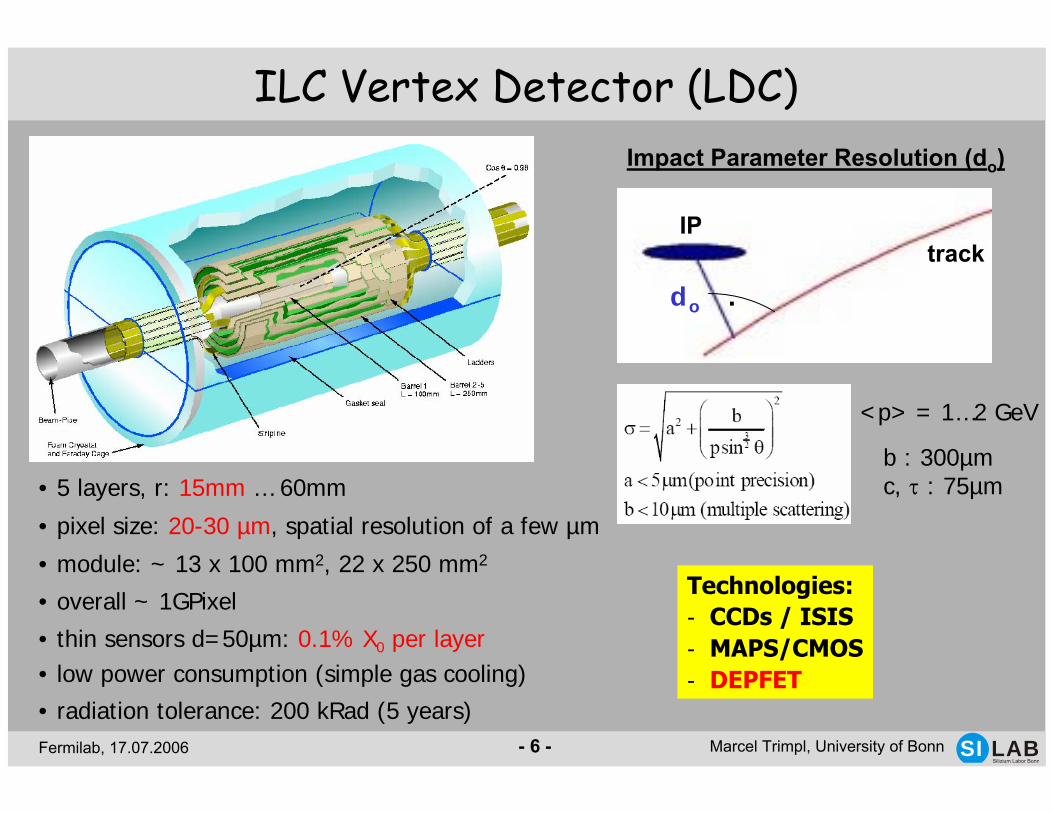
ILC Vertex Detector (LDC)
do .do .
Impact Parameter Resolution (do)
IPtrack
• 5 layers, r: 15mm … 60mm
• pixel size: 20-30 µm, spatial resolution of a few µm
• module: ~ 13 x 100 mm2, 22 x 250 mm2
• overall ~ 1GPixel
• thin sensors d=50µm: 0.1% X0 per layer• low power consumption (simple gas cooling)• radiation tolerance: 200 kRad (5 years)
<p> = 1…2 GeV
b : 300µmc, τ : 75µm
Fermilab, 17.07.2006 LABSilizium Labor Bonn
SIMarcel Trimpl, University of Bonn- 7 -
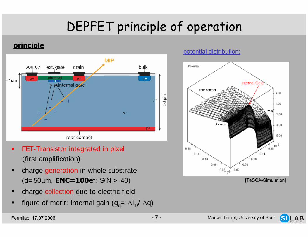
DEPFET principle of operation
FET-Transistor integrated in pixel(first amplification)
charge generation in whole substrate (d=50µm, ENC=100e-: S/N > 40)
charge collection due to electric field
figure of merit: internal gain (gq= ∆ID/ ∆q)
principle
internal Gate
potential distribution:
Drain
Source
rear contact
[TeSCA-Simulation]
Fermilab, 17.07.2006 LABSilizium Labor Bonn
SIMarcel Trimpl, University of Bonn- 8 -
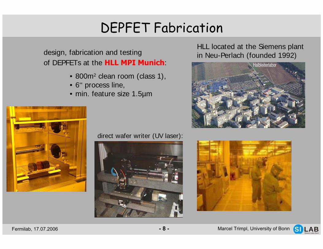
DEPFET Fabricationdesign, fabrication and testing of DEPFETs at the HLL MPI Munich:
direct wafer writer (UV laser):
HLL located at the Siemens plant in Neu-Perlach (founded 1992)
• 800m2 clean room (class 1),• 6‘‘ process line, • min. feature size 1.5µm
Fermilab, 17.07.2006 LABSilizium Labor Bonn
SIMarcel Trimpl, University of Bonn- 9 -
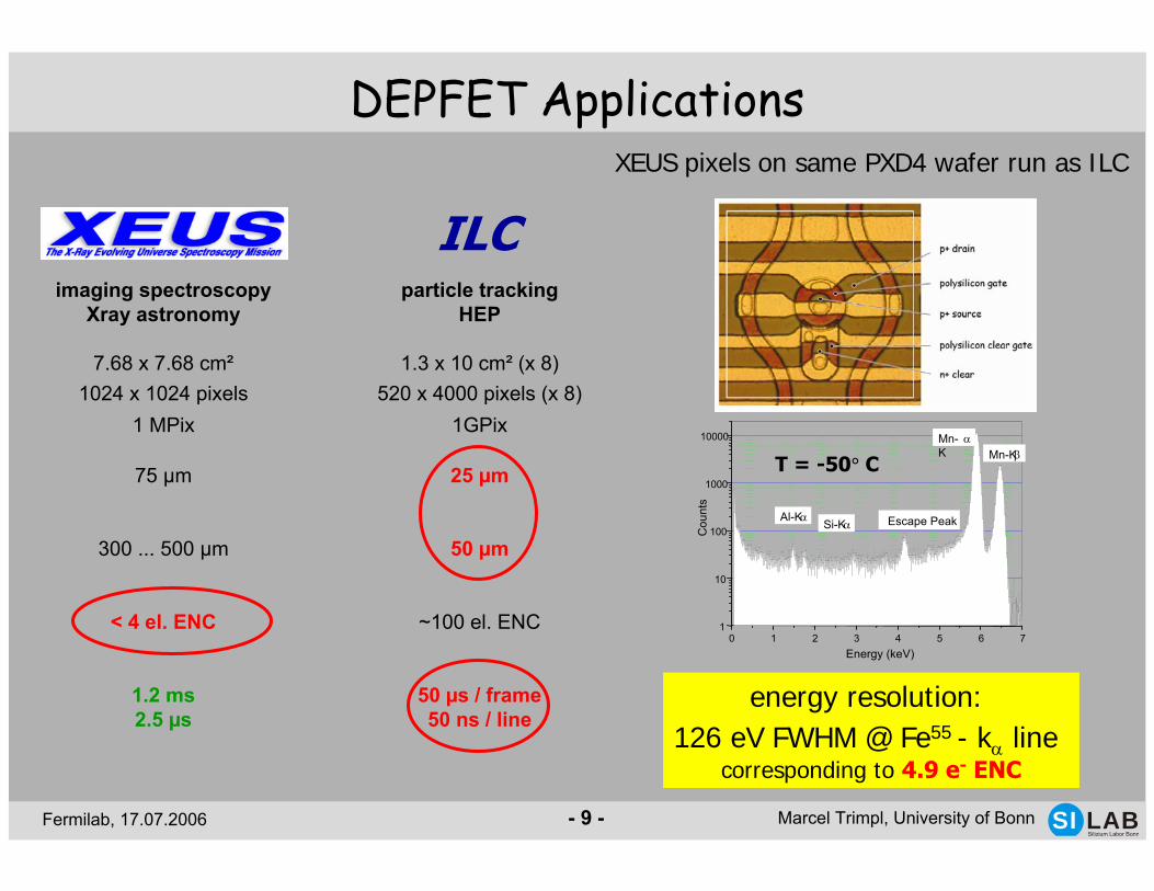
DEPFET Applications
particle trackingHEP
1.3 x 10 cm² (x 8)520 x 4000 pixels (x 8)
1GPix
25 µm
50 µm
~100 el. ENC
50 µs / frame50 ns / line
imaging spectroscopyXray astronomy
7.68 x 7.68 cm²1024 x 1024 pixels
1 MPix
75 µm
300 ... 500 µm
< 4 el. ENC
1.2 ms2.5 µs
XEUS pixels on same PXD4 wafer run as ILC
ILC
energy resolution: 126 eV FWHM @ Fe55 - kα line
corresponding to 4.9 e- ENC
0 1 2 3 4 5 6 71
10
100
1000
10000
Si-KαAl-Kα
Mn-KβMn-K
α
Cou
nts
Energy (keV)
Escape Peak
T = -50° C

Fermilab, 17.07.2006 LABSilizium Labor Bonn
SIMarcel Trimpl, University of Bonn- 10 -
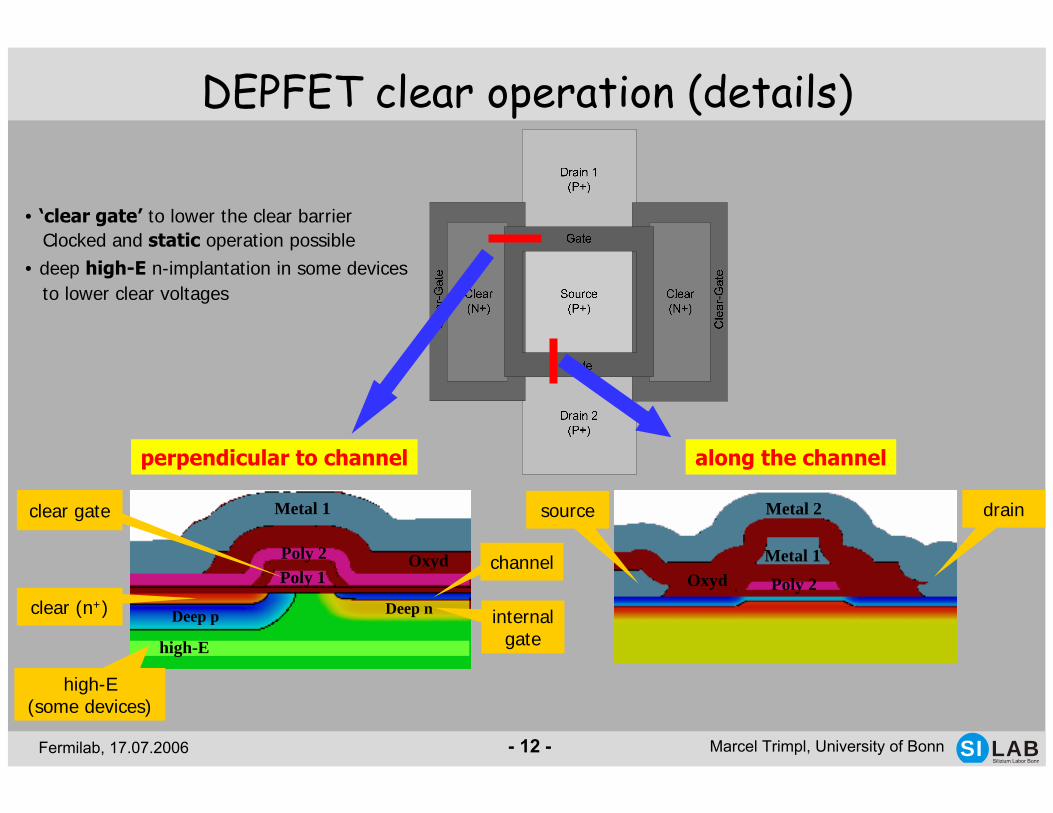
sensor production for the ILC
gate
clear
drai
nfabricated: matrices with up to 128x64 pixel, 450µm thick
linear double pixel structures (22x36 µm2 pixels) (high density layout)
• new production started recently 03/2006:• matrices up to 512x512 pixel• full ILC length column & row test structures
special clear gate to support clear operation
gate
clear
source
drain 1 drain 2
also: clear gate
Fermilab, 17.07.2006 LABSilizium Labor Bonn
SIMarcel Trimpl, University of Bonn- 11 -
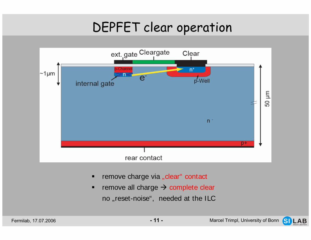
DEPFET clear operation
remove charge via „clear“ contactremove all charge complete clear
no „reset-noise“, needed at the ILC
Fermilab, 17.07.2006 LABSilizium Labor Bonn
SIMarcel Trimpl, University of Bonn- 12 -
source drain
channel
internalgate
clear gate
clear (n+)
high-E(some devices)
DEPFET clear operation (details)
perpendicular to channel along the channel
• ‘clear gate’ to lower the clear barrier Clocked and static operation possible
• deep high-E n-implantation in some devices to lower clear voltages
Deep nDeep p
Poly 1Poly 2
Metal 1
Oxyd Metal 1
Metal 2
Poly 2Oxyd
high-E

Fermilab, 17.07.2006 LABSilizium Labor Bonn
SIMarcel Trimpl, University of Bonn- 13 -
• complete clear achieved with static clear gate!• required voltages small (5 – 7 V) –
important for future SWITCHER!• clear (gate) operation does not decrease after irradiation (1MRad)
(Clear off = 2V)0 20 40 60 80 100 120 140 160 180 200 220
14
15
16
17
18
19
20
21
22
UClear-on = 8V UClear-on = 10V UClear-on = 14V σ N
OIS
E [n
A]
∆ t (Clear) [ns]
Complete clear in only 10 ns:• Measurements on mini matrix devices• ‘noise’ becomes minimal if
clearing is complete!
UClear-off = 3 Vregion of
complete clear
high-E
clear efficiency
• various designs (high-E, no high-E)• geometries (length of clear gate) • operating conditions (static or clocked clear gate)
static!
[C.Sandow, Bonn]
Fermilab, 17.07.2006 LABSilizium Labor Bonn
SIMarcel Trimpl, University of Bonn- 14 -
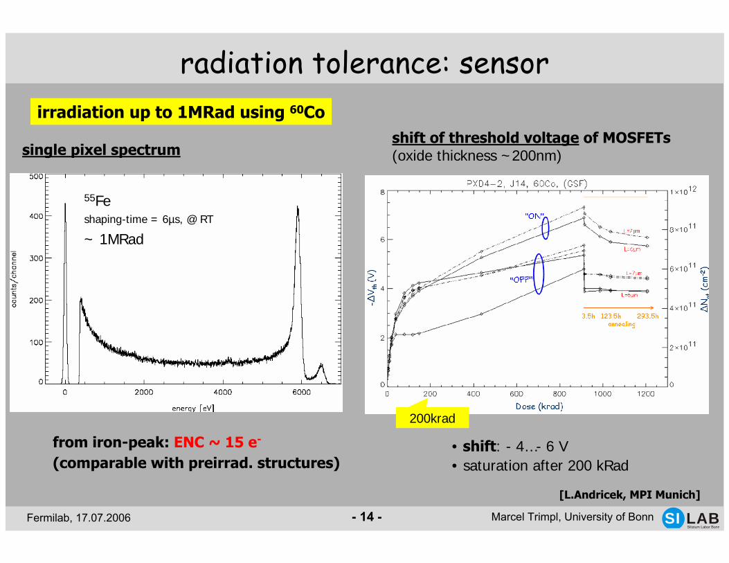
radiation tolerance: sensor
200krad
shift of threshold voltage of MOSFETs(oxide thickness ~200nm)
• shift: - 4…- 6 V• saturation after 200 kRad
shaping-time = 6µs, @ RT
single pixel spectrum
from iron-peak: ENC ~ 15 e-
(comparable with preirrad. structures)
55Fe
~ 1MRad
irradiation up to 1MRad using 60Co
[L.Andricek, MPI Munich]
Fermilab, 17.07.2006 LABSilizium Labor Bonn
SIMarcel Trimpl, University of Bonn- 15 -
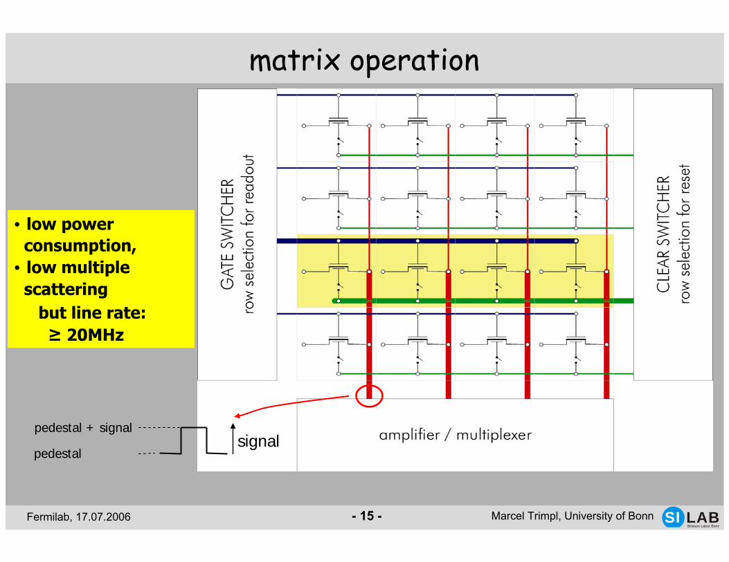
matrix operation
signalpedestal
pedestal + signal
• low powerconsumption,
• low multiplescattering
but line rate: ≥ 20MHz
Fermilab, 17.07.2006 LABSilizium Labor Bonn
SIMarcel Trimpl, University of Bonn- 16 -
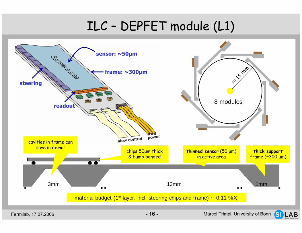
r=15
mm
8 modules
frame: ~300µm
sensor: ~50µm
readout
steering
ILC – DEPFET module (L1)
cavities in frame can save material
thick supportframe (~300 µm)
material budget (1st layer, incl. steering chips and frame) ~ 0.11 %X0
13mm 1mm3mm
thinned sensor (50 µm) in active area
chips 50µm thick & bump bonded
Fermilab, 17.07.2006 LABSilizium Labor Bonn
SIMarcel Trimpl, University of Bonn- 17 -
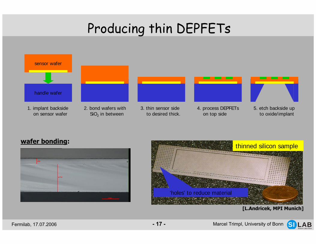
Producing thin DEPFETs
wafer bonding:
‘holes’ to reduce material
thinned silicon sample
[L.Andricek, MPI Munich]
sensor wafer
handle wafer
1. implant backsideon sensor wafer
2. bond wafers withSiO2 in between
3. thin sensor sideto desired thick.
4. process DEPFETson top side
5. etch backside upto oxide/implant
Fermilab, 17.07.2006 LABSilizium Labor Bonn
SIMarcel Trimpl, University of Bonn- 18 -
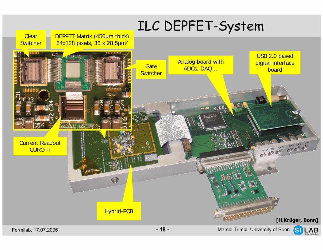
Current Readout CURO II
Gate Switcher
ClearSwitcher
DEPFET Matrix (450µm thick)64x128 pixels, 36 x 28.5µm2
ILC DEPFET-System
USB 2.0 based digital interface
boardAnalog board with
ADCs, DAQ …
Hybrid-PCB[H.Krüger, Bonn]
Fermilab, 17.07.2006 LABSilizium Labor Bonn
SIMarcel Trimpl, University of Bonn- 19 -
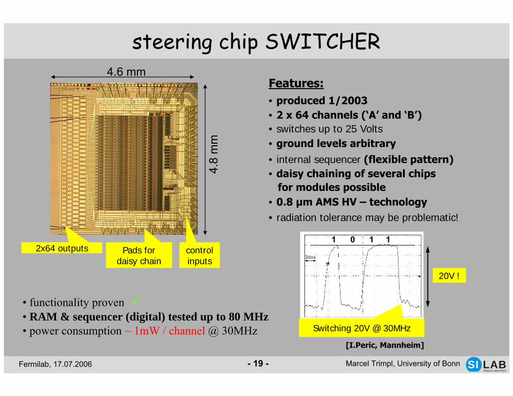
steering chip SWITCHER4.6 mm
4.8
mm
[I.Peric, Mannheim]
1 0 1 1
∆U = 20V ν = 30 MHz
20ns
20V !
Switching 20V @ 30MHz
Pads for daisy chain
controlinputs
2x64 outputs
• functionality proven • RAM & sequencer (digital) tested up to 80 MHz• power consumption ~ 1mW / channel @ 30MHz
Features:• produced 1/2003 • 2 x 64 channels (‘A’ and ‘B’)• switches up to 25 Volts• ground levels arbitrary• internal sequencer (flexible pattern)• daisy chaining of several chips
for modules possible• 0.8 µm AMS HV – technology• radiation tolerance may be problematic!
Fermilab, 17.07.2006 LABSilizium Labor Bonn
SIMarcel Trimpl, University of Bonn- 20 -
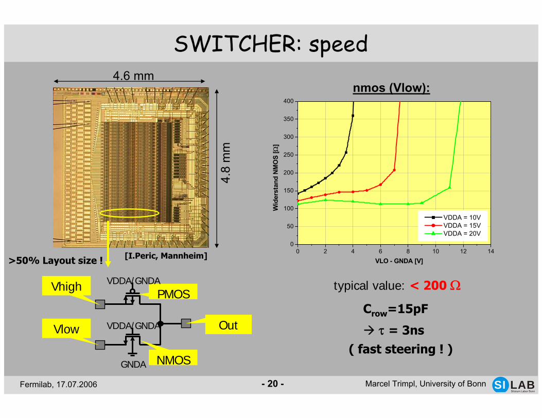
SWITCHER: speed4.6 mm
4.8
mm
0 2 4 6 8 10 12 140
50
100
150
200
250
300
350
400
VDDA = 10V VDDA = 15V VDDA = 20V
Wid
erst
and
NM
OS
[ Ω]
VLO - GNDA [V]
typical value: < 200 Ω
nmos (Vlow):
PMOS
GNDA
Out VDDA/GNDA
VDDA/GNDA
NMOS
Vhigh
Vlow
>50% Layout size !
Crow=15pF
τ = 3ns( fast steering ! )
[I.Peric, Mannheim]
Fermilab, 17.07.2006 LABSilizium Labor Bonn
SIMarcel Trimpl, University of Bonn- 21 -
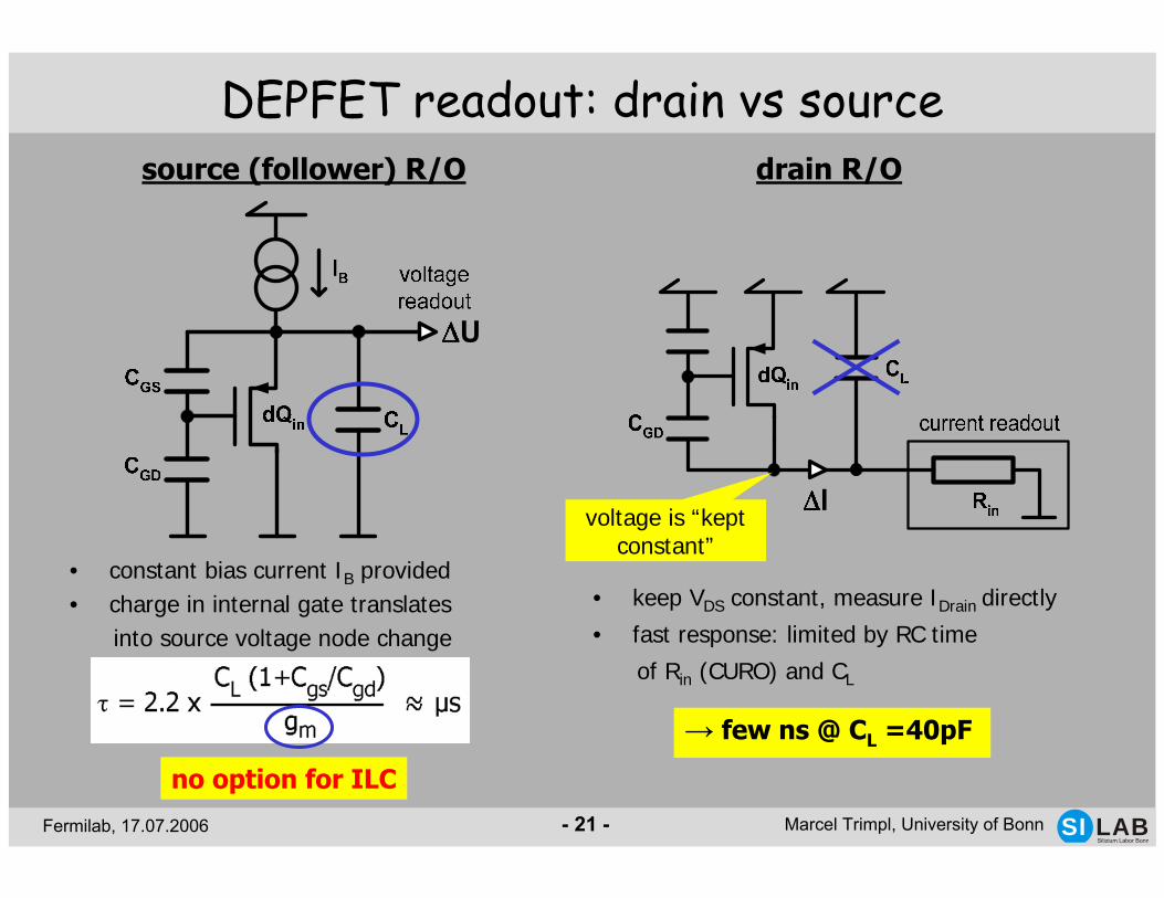
DEPFET readout: drain vs sourcesource (follower) R/O drain R/O
voltage is “keptconstant”
• keep VDS constant, measure IDrain directly
• fast response: limited by RC time
of Rin (CURO) and CL
• constant bias current IB provided• charge in internal gate translates
into source voltage node change
no option for ILC
→ few ns @ CL =40pF
Fermilab, 17.07.2006 LABSilizium Labor Bonn
SIMarcel Trimpl, University of Bonn- 22 -
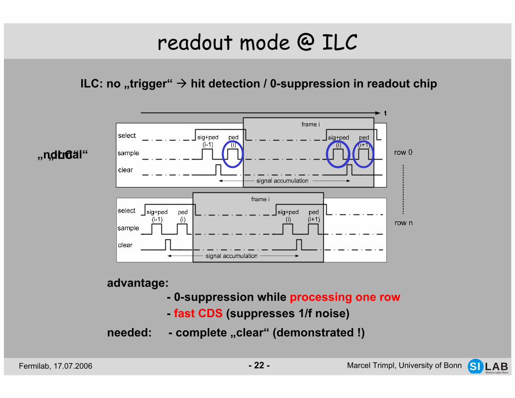
advantage: - 0-suppression while processing one row- fast CDS (suppresses 1/f noise)
needed: - complete „clear“ (demonstrated !)
readout mode @ ILC
ILC: no „trigger“ hit detection / 0-suppression in readout chip
„normal“„ILC“
Fermilab, 17.07.2006 LABSilizium Labor Bonn
SIMarcel Trimpl, University of Bonn- 23 -
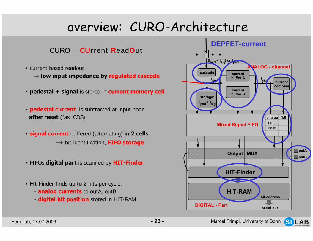
cascode currentbuffer A
currentbuffer B
HIT-Finder
HIT-RAM
storage:Iped + Isig
currentcompare
serial-out
1/0
hit-address
analogFIFOcells
(Iped + Isig) or Iped
IsigIsig
outA
outB
DIGITAL - Part
ANALOG - channel
Output MUX
Mixed Signal FIFO
• current based readout→ low input impedance by regulated cascode
• Hit-Finder finds up to 2 hits per cycle:- analog currents to outA, outB- digital hit position stored in HIT-RAM
• FIFOs digital part is scanned by HIT-Finder
• signal current buffered (alternating) in 2 cells
→ hit-identification, FIFO storage
• pedestal current is subtracted at input node after reset (fast CDS)
• pedestal + signal is stored in current memory cell
overview: CURO-ArchitectureCURO – CUrrent ReadOut
DEPFET-current
Fermilab, 17.07.2006 LABSilizium Labor Bonn
SIMarcel Trimpl, University of Bonn- 24 -
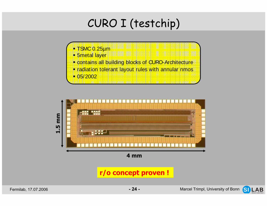
CURO I (testchip)
4 mm
1.5
mm
TSMC 0.25µm5metal layercontains all building blocks of CURO-Architectureradiation tolerant layout rules with annular nmos05/2002
r/o concept proven !
Fermilab, 17.07.2006 LABSilizium Labor Bonn
SIMarcel Trimpl, University of Bonn- 25 -
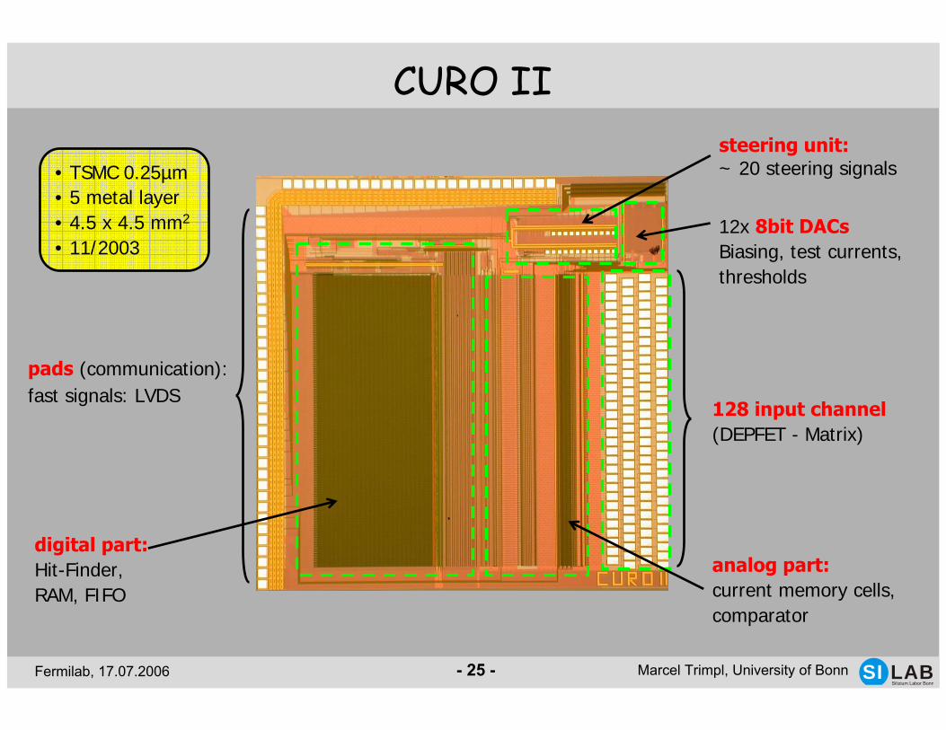
CURO II
128 input channel(DEPFET - Matrix)
12x 8bit DACsBiasing, test currents, thresholds
pads (communication):fast signals: LVDS
steering unit:~ 20 steering signals• TSMC 0.25µm
• 5 metal layer• 4.5 x 4.5 mm2
• 11/2003
analog part:current memory cells,comparator
digital part:Hit-Finder, RAM, FIFO
Fermilab, 17.07.2006 LABSilizium Labor Bonn
SIMarcel Trimpl, University of Bonn- 26 -
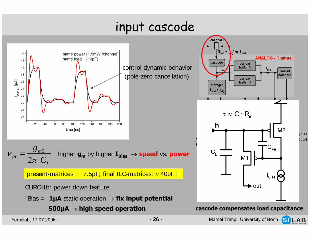
input cascode
τ ≈ CL. Rin
present-matrices : 7.5pF; final ILC-matrices: ≈ 40pF !!
cascode compensates load capacitance
0 20 40 60 80 100 120 140 160 180 200
26
28
30
32
34
36
38
40
42
44 same power (1.5mW /channel)same load (10pF)
I DEP
FET [
µA]
time [ns]
control dynamic behavior(pole-zero cancellation)
L
mgr C
gπ
ν2
2=
CUROIIb: power down feature
IBias = 1µA static operation → fix input potential
500µA → high speed operation
higher gm by higher IBias → speed vs. power
Fermilab, 17.07.2006 LABSilizium Labor Bonn
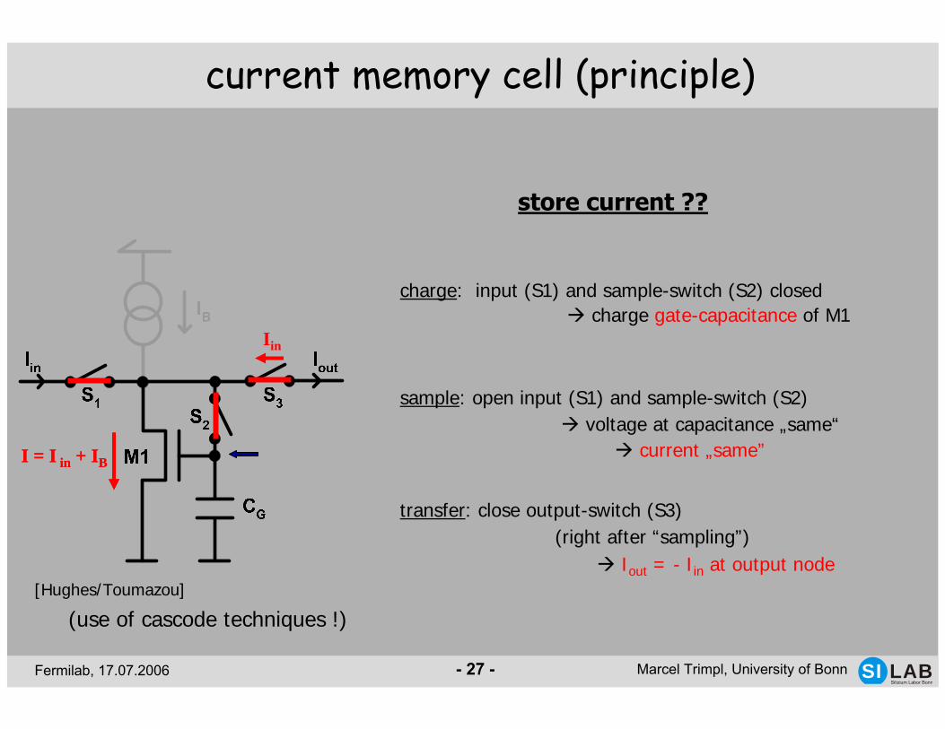
SIMarcel Trimpl, University of Bonn- 27 -
charge: input (S1) and sample-switch (S2) closedcharge gate-capacitance of M1
Iin
transfer: close output-switch (S3) (right after “sampling”)
Iout = - Iin at output node
sample: open input (S1) and sample-switch (S2)voltage at capacitance „same“
current „same”I = I in + IB
store current ??
I = I in + IB
current memory cell (principle)
[Hughes/Toumazou]
(use of cascode techniques !)
Fermilab, 17.07.2006 LABSilizium Labor Bonn
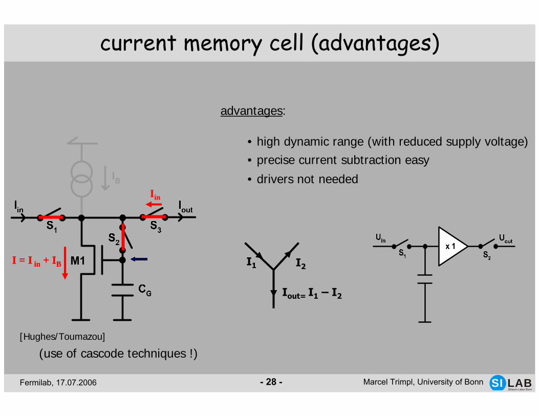
SIMarcel Trimpl, University of Bonn- 28 -
I1 I2
Iout= I1 – I2
current memory cell (advantages)
advantages:
• high dynamic range (with reduced supply voltage)• precise current subtraction easy
• drivers not neededIin
I = I in + IBI = I in + IB
[Hughes/Toumazou]
(use of cascode techniques !)
Fermilab, 17.07.2006 LABSilizium Labor Bonn
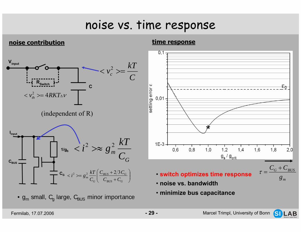
SIMarcel Trimpl, University of Bonn- 29 -
Gm C
kTgi 22 >≈<1/gS
CG
CBUS
Iinput
CRSwitch
Vinput
(independent of R)
CkTvc >=< 2
ν∆>=< RKTvth 42
⎟⎟⎠
⎞⎜⎜⎝
⎛+
+>=<
GBUS
GBUS
Gm CC
CCCkTgi 3222
noise contribution time response
m
BUSG
gCC +
=τ• switch optimizes time response• noise vs. bandwidth• minimize bus capacitance
• gm small, Cg large, CBUS minor importance
noise vs. time response
Fermilab, 17.07.2006 LABSilizium Labor Bonn
SIMarcel Trimpl, University of Bonn- 30 -
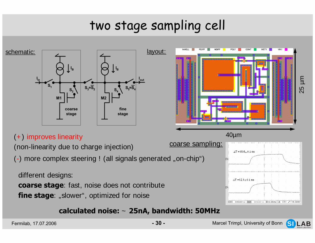
layout:
two stage sampling cell
25 µ
m
40µm(+) improves linearity(non-linearity due to charge injection)
(-) more complex steering ! (all signals generated „on-chip“)
M1
IinS1
S2S3=S2
IB
M2
Iout
S4S5=S4
IB
coarsestage
finestage
calculated noise: ~ 25nA, bandwidth: 50MHz
different designs: coarse stage: fast, noise does not contributefine stage: „slower“, optimized for noise
schematic:
coarse sampling:
Fermilab, 17.07.2006 LABSilizium Labor Bonn
SIMarcel Trimpl, University of Bonn- 31 -
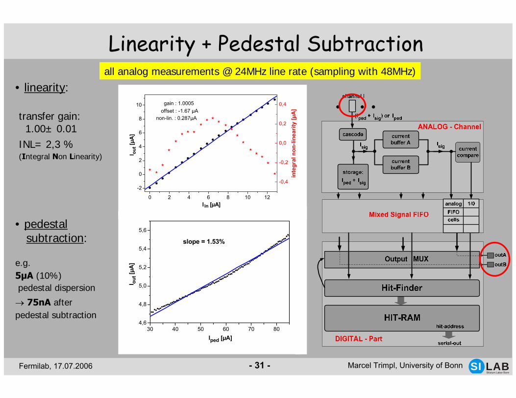
Linearity + Pedestal Subtraction
• linearity:
• pedestalsubtraction:
transfer gain: 1.00± 0.01
INL= 2,3 %(Integral Non Linearity)
0 2 4 6 8 10 12
-2
0
2
4
6
8
10
-0,4
-0,2
0,0
0,2
0,4
I in [µA]
I out
[µA
]
gain : 1.0005
non-lin. : 0.287µAoffset : -1.67 µA
inte
gral
non
-line
arity
[µA
]
e.g.5µA (10%)pedestal dispersion
→ 75nA after pedestal subtraction
30 40 50 60 70 804,6
4,8
5,0
5,2
5,4
5,6
I out
[µA
]
Iped [µA]
slope = 1.53%
all analog measurements @ 24MHz line rate (sampling with 48MHz)
Fermilab, 17.07.2006 LABSilizium Labor Bonn
SIMarcel Trimpl, University of Bonn- 32 -
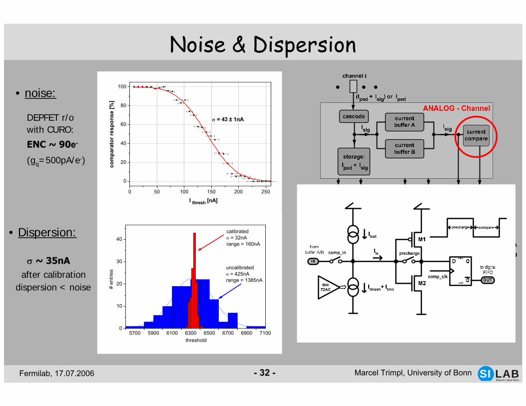
Noise & Dispersion
• noise:
• Dispersion:
DEPFET r/owith CURO:
ENC ~ 90e-
(gq=500pA/e-)
σ ~ 35nAafter calibration
dispersion < noise
0 50 100 150 200 250
0
20
40
60
80
100
σ = 43 ± 1nAco
mpa
rato
r res
pons
e [%
]
I thresh [nA]
5700 5900 6100 6300 6500 6700 6900 71000
10
20
30
40
# en
tries
threshold
calibratedσ = 32nArange = 160nA
uncalibratedσ = 425nArange = 1385nA
Fermilab, 17.07.2006 LABSilizium Labor Bonn
SIMarcel Trimpl, University of Bonn- 33 -
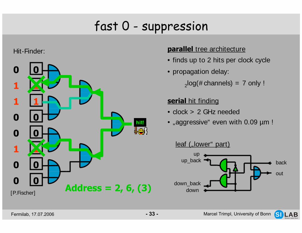
fast 0 - suppression
0
1
1
0
0
1
0
0
0
1
1
0
0
1
0
0Address = 2, 6, (3)
parallel tree architecture
• finds up to 2 hits per clock cycle
• propagation delay:
2log(#channels) = 7 only !
serial hit finding
• clock > 2 GHz needed• „aggressive“ even with 0.09 µm !
Hit-Finder:
out
back
up
downdown_back
up_back
leaf („lower“ part)
[P.Fischer]
Fermilab, 17.07.2006 LABSilizium Labor Bonn
SIMarcel Trimpl, University of Bonn- 34 -
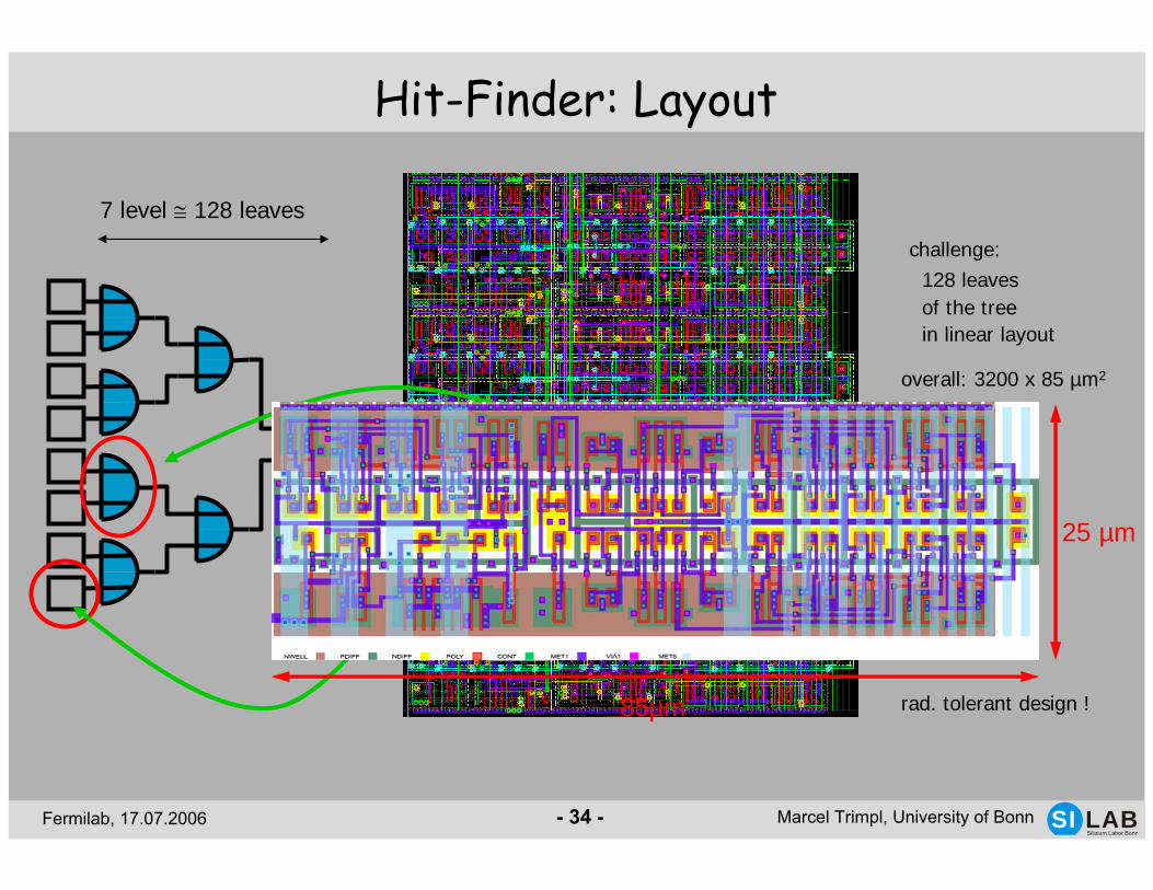
Hit-Finder: Layout
challenge: 128 leaves of the tree in linear layout
7 level ≅ 128 leaves
overall: 3200 x 85 µm2
85µm
25 µm
rad. tolerant design !
Fermilab, 17.07.2006 LABSilizium Labor Bonn
SIMarcel Trimpl, University of Bonn- 35 -
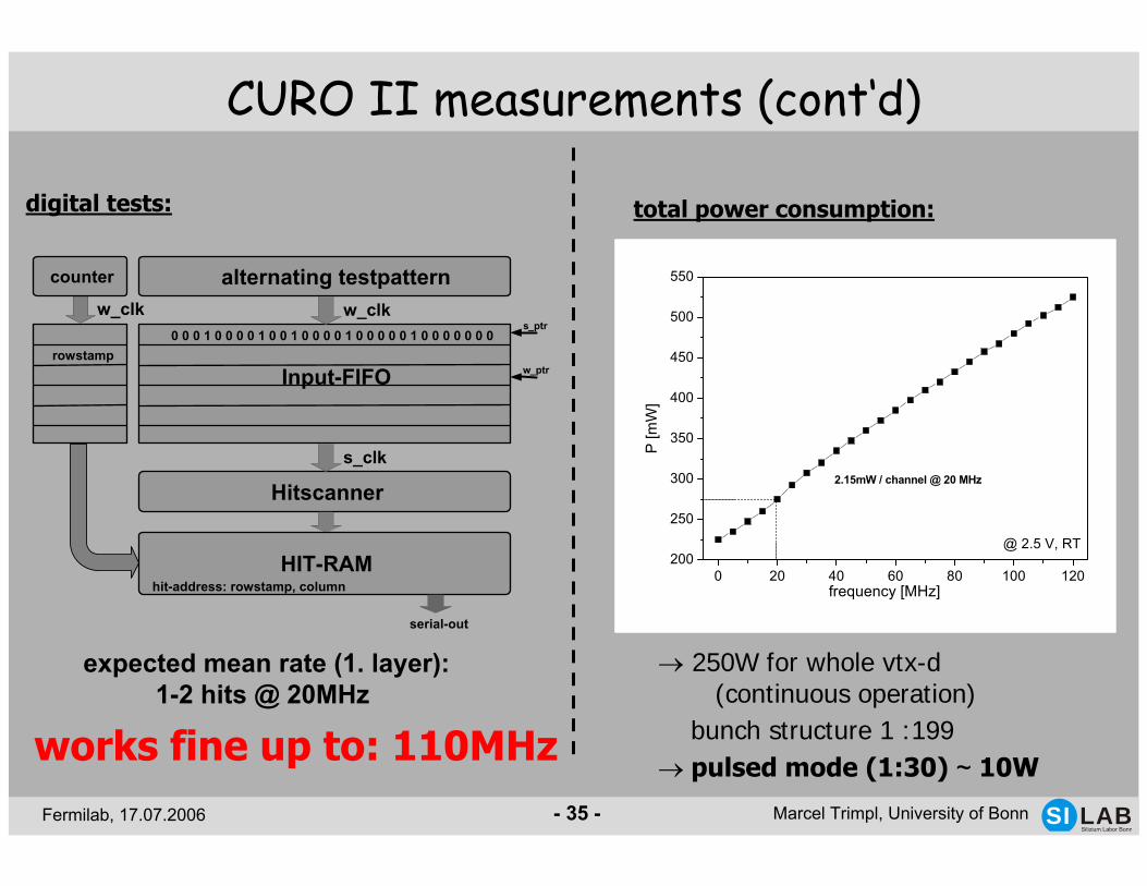
works fine up to: 110MHz
total power consumption:digital tests:
→ 250W for whole vtx-d(continuous operation)
bunch structure 1 :199→ pulsed mode (1:30) ~ 10W
CURO II measurements (cont‘d)
Hitscanner
HIT-RAM
serial-out
hit-address: rowstamp, column
Input-FIFO
alternating testpatternw_clk
s_clk
s_ptr
w_ptr
w_clk
counter
rowstamp0 0 0 1 0 0 0 0 1 0 0 1 0 0 0 0 1 0 0 0 0 0 1 0 0 0 0 0 0 0
expected mean rate (1. layer): 1-2 hits @ 20MHz
0 20 40 60 80 100 120200
250
300
350
400
450
500
550
2.15mW / channel @ 20 MHz
@ 2.5 V, RT
P [m
W]
frequency [MHz]

Fermilab, 17.07.2006 LABSilizium Labor Bonn
SIMarcel Trimpl, University of Bonn- 36 -
System Measurements
Fermilab, 17.07.2006 LABSilizium Labor Bonn
SIMarcel Trimpl, University of Bonn- 37 -
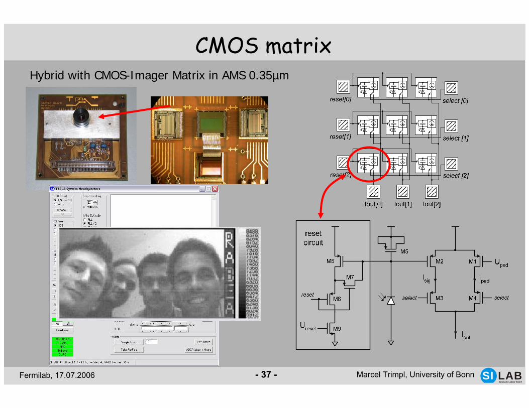
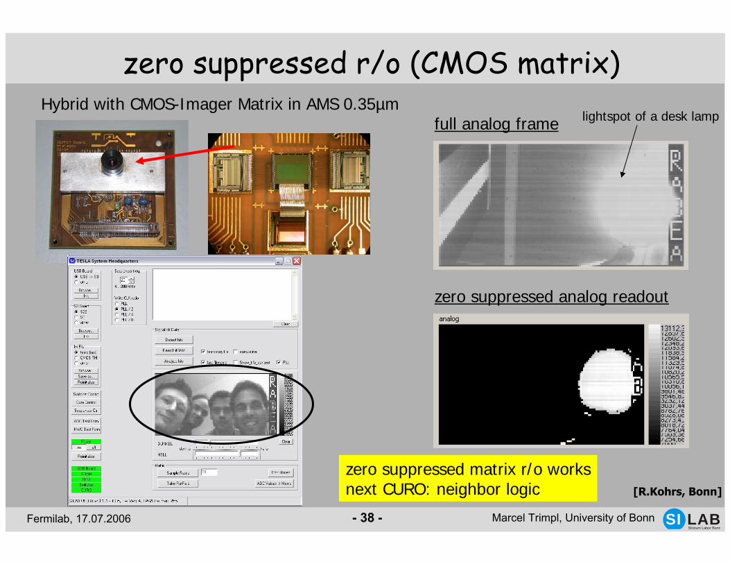
CMOS matrixHybrid with CMOS-Imager Matrix in AMS 0.35µm
Fermilab, 17.07.2006 LABSilizium Labor Bonn
SIMarcel Trimpl, University of Bonn- 38 -
zero suppressed matrix r/o worksnext CURO: neighbor logic
zero suppressed r/o (CMOS matrix)lightspot of a desk lamp
Hybrid with CMOS-Imager Matrix in AMS 0.35µmfull analog frame
zero suppressed analog readout
[R.Kohrs, Bonn]

Fermilab, 17.07.2006 LABSilizium Labor Bonn
SIMarcel Trimpl, University of Bonn- 39 -
35 40 45 50 55 60 65 70 75 80 850
250
500
750
1000
1250
1500
1750
2000
2250
# en
tries
Eγ [keV]
FAUST100 um 50 um 25 um75 um
2 m
m
3 mm
ILC DEPFET-System in the lab
irradiation with 55Fe(6keV γ, 1700 e-)
75 µm thick Tungsten-Mask
10 15 20 25 30 35 40 45100
200
300
400
500
600
-4
-2
0
2
4
sign
al [A
DU
]
Eγ [keV]
Ag/Cd
Ba
Tb
Rb
Mo
INL = 0.75% (8500e- dyn. Range)
non-
linea
rity
[AD
U]
gq = 280 pA / e-
system performance:
• speed: line rate ~2 MHz• noise: 220 e- (from noise peak)
Integral-Non-Linearity = 0.75% for 8500e-
241Am
Fermilab, 17.07.2006 LABSilizium Labor Bonn
SIMarcel Trimpl, University of Bonn- 40 -
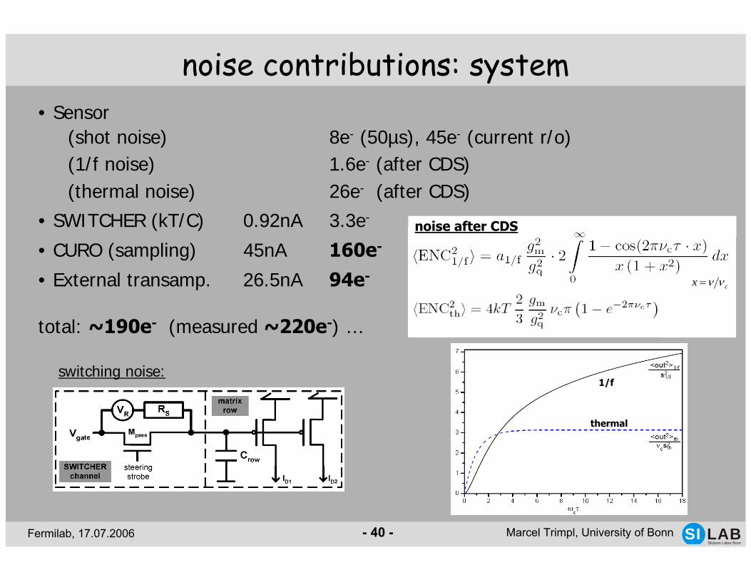
noise contributions: system• Sensor
(shot noise) 8e- (50µs), 45e- (current r/o)(1/f noise) 1.6e- (after CDS)(thermal noise) 26e- (after CDS)
• SWITCHER (kT/C) 0.92nA 3.3e-
• CURO (sampling) 45nA 160e-
• External transamp. 26.5nA 94e-
total: ~190e- (measured ~220e-) …
thermal
1/f
noise after CDS
switching noise:
cx νν=
Fermilab, 17.07.2006 LABSilizium Labor Bonn
SIMarcel Trimpl, University of Bonn- 41 -
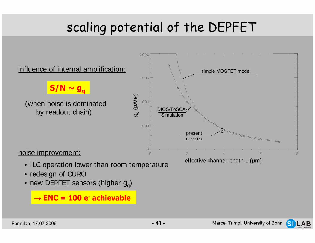
influence of internal amplification:
(when noise is dominated by readout chain)
scaling potential of the DEPFET
effective channel length L (µm)
g q(p
A/e-
)presentdevices
DIOS/ToSCA-Simulation
simple MOSFET model
S/N ~ gq
• ILC operation lower than room temperature• redesign of CURO • new DEPFET sensors (higher gq)
noise improvement:
→ ENC = 100 e- achievable
Fermilab, 17.07.2006 LABSilizium Labor Bonn
SIMarcel Trimpl, University of Bonn- 42 -
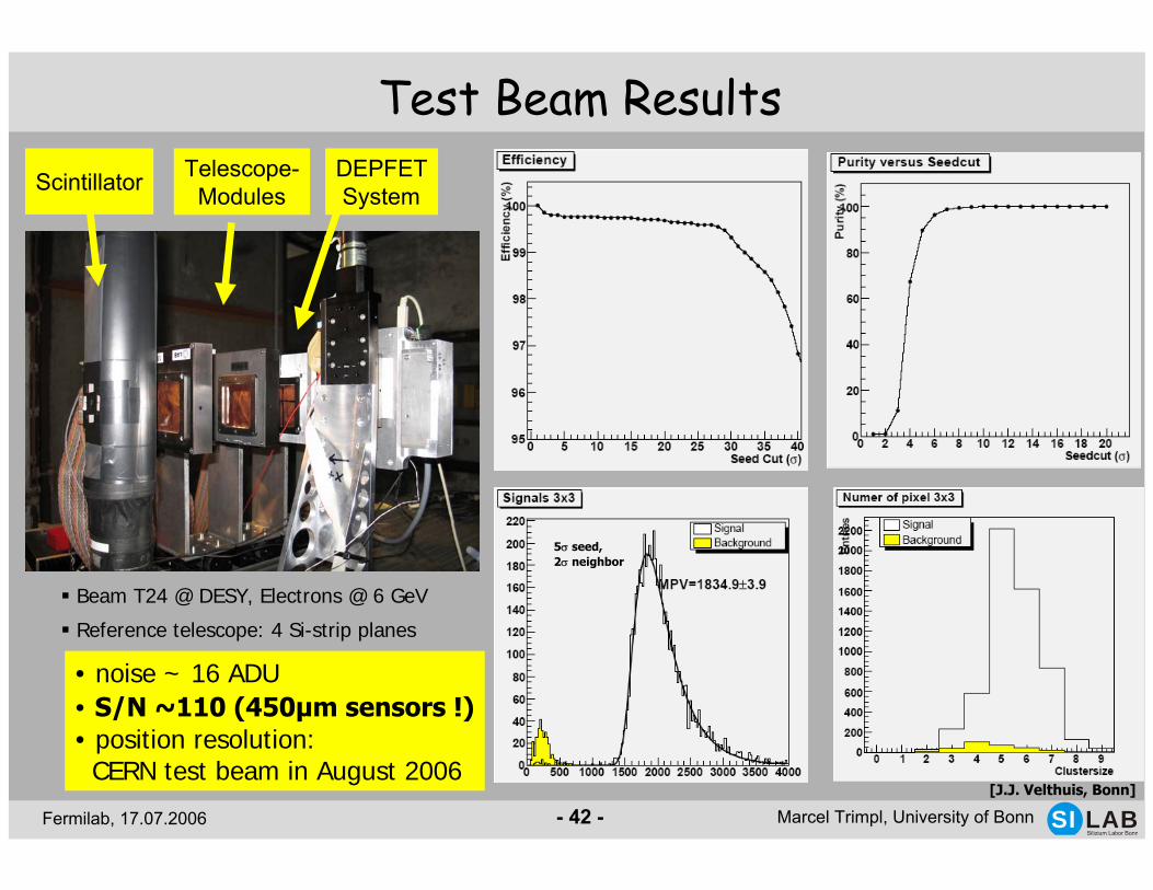
Test Beam ResultsScintillator Telescope-
ModulesDEPFETSystem
Beam T24 @ DESY, Electrons @ 6 GeV
Reference telescope: 4 Si-strip planes
• noise ~ 16 ADU• S/N ~110 (450µm sensors !)• position resolution:
CERN test beam in August 2006[J.J. Velthuis, Bonn]
5σ seed,2σ neighbor
Fermilab, 17.07.2006 LABSilizium Labor Bonn
SIMarcel Trimpl, University of Bonn- 43 -
summary
• DEPFET pixel based vtx-d presented- features: high S/N due to fully depleted bulk- present production (~30x30µm2 pixels, matrices: 128x64 pixels, 450µm thick)- clear, radiation tolerance demonstrated, thinning concept established
• Readout ASIC (CURO) using current mode techniques:- pedestal subtraction, fast CDS, on chip hit-detection and 0-suppression
• CURO II performance:- noise: < 45nA → ∼ 160 e- (gq=280pA/e-) / 90e- (gq=500pA/e- ≅ design value)- analog speed: 24 MHz line rate (48MSPS) , sufficient for ILC !- hit-identification and 0-suppression : > 100MHz , sufficient for ILC !
• ILC-DEPFET-System:- operated at ≈ 2MHz line rate, noise: 220e-
- 6GeV e- test beam at DESY: S/N ∼ 110 (450µm sensors)
Fermilab, 17.07.2006 LABSilizium Labor Bonn
SIMarcel Trimpl, University of Bonn- 44 -
outlook
System:• increase system speed (2MHz → 20MHz !!)• reduce noise (190e- possible, next system should achieve <100e- )• beam test @ CERN -> spatial resolution and establish pixel telescope
CURO IIb:• on-chip common mode computation/correction (easy with currents)• cluster logic (keeping at least the closest neighbor)• improve input cascode (readout larger matrices)• implement (fast) power down feature (pulsed mode configuration)• on chip ADC (IP from nordic semiconductor)
New sensors:• 512x512 matrices, 25x25µm2
• production of thin DEPFETs (longer time scale)
Fermilab, 17.07.2006 LABSilizium Labor Bonn
SIMarcel Trimpl, University of Bonn- 45 -
referencesReferencesCURO / System: „Design of a current based readout chip and development of a DEPFET pixel
prototype system for the ILC vertex detector“, PhD thesis, M.Trimpl, http://hss.ulb.uni-bonn.de/diss_onlineThinning: „Processing of ultra thin silicon sensors for future linear collider experiments“, L.Andricek et al.,
IEEE TNS (51), No3, pp.1117-1120Sensor: „Design and Technology of DEPFET Pixel Sensors for Linear Collider Applicatons“, R.H.Richter,
NIM A511, pp.250-256Rad Tolerance: „The MOS-type DEPFET Pixel Sensor for the ILC Environment“, L.Andircek et al.,
Pixel 2005, submitted to NIM (A)
Fermilab, 17.07.2006 LABSilizium Labor Bonn
SIMarcel Trimpl, University of Bonn- 46 -
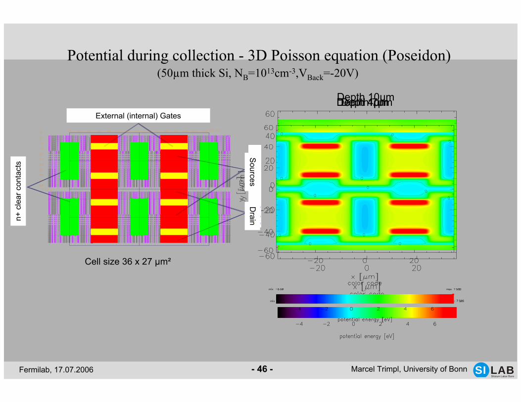
Potential during collection - 3D Poisson equation (Poseidon)(50µm thick Si, NB=1013cm-3,VBack=-20V)
Depth 10µmDepth 7µmDepth 4µmDepth 1µm
Sources
Drain
External (internal) Gates
n+ c
lear
cont
acts
Cell size 36 x 27 µm²
Fermilab, 17.07.2006 LABSilizium Labor Bonn
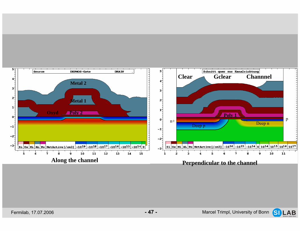
SIMarcel Trimpl, University of Bonn- 47 -
Along the channel Perpendicular to the channel
Metal 2
Metal 1
Oxyd Poly 2
Clear Gclear Channnel
pDeep nn+
Deep p
Poly 1

Fermilab, 17.07.2006 LABSilizium Labor Bonn
SIMarcel Trimpl, University of Bonn- 48 -
d) anisotropic etching from backside (TMAH)
open backside passivation
c) process passivation
b) wafer bonding and grinding/polishing of top wafer
a) oxidation and back side implant of top wafer
Handle <100> Wafer
Top Wafer
Fermilab, 17.07.2006 LABSilizium Labor Bonn
SIMarcel Trimpl, University of Bonn- 49 -
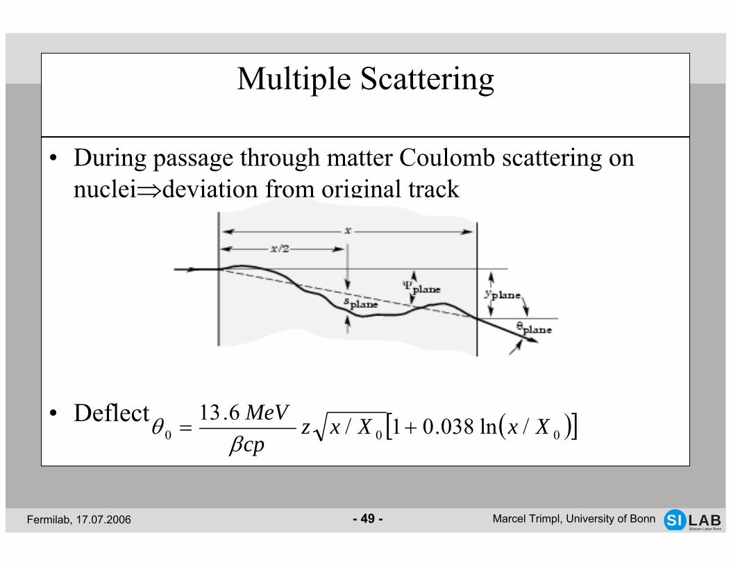
Multiple Scattering
• During passage through matter Coulomb scattering on nuclei⇒deviation from original track
• Deflection distribution Gaussian with width θ0( )[ ]000 /ln038.01/6.13 XxXxzcp MeV
+=β
θ
Fermilab, 17.07.2006 LABSilizium Labor Bonn
SIMarcel Trimpl, University of Bonn- 50 -
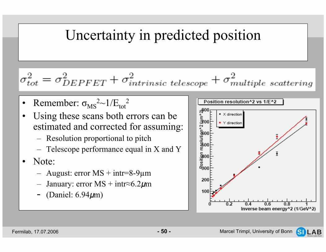
Uncertainty in predicted position
• Remember: σMS2~1/Etot
2
• Using these scans both errors can be estimated and corrected for assuming:– Resolution proportional to pitch– Telescope performance equal in X and Y
• Note:– August: error MS + intr=8-9µm– January: error MS + intr≈6.2µm– (Daniel: 6.94µm)
Fermilab, 17.07.2006 LABSilizium Labor Bonn
SIMarcel Trimpl, University of Bonn- 51 -
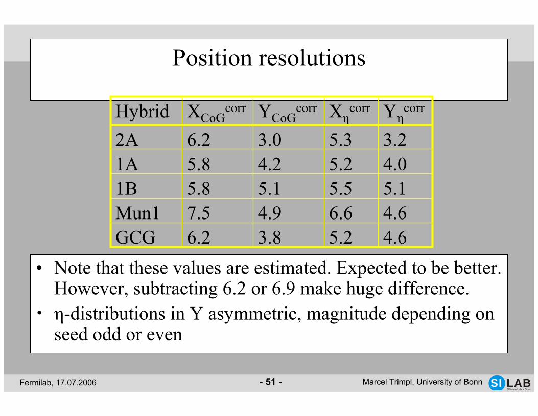
Position resolutions
4.65.23.86.2GCG4.66.64.97.5Mun15.15.55.15.81B4.05.24.25.81A3.25.33.06.22AYη
corrXηcorrYCoG
corrXCoGcorrHybrid
• Note that these values are estimated. Expected to be better. However, subtracting 6.2 or 6.9 make huge difference.
• η-distributions in Y asymmetric, magnitude depending on seed odd or even
Fermilab, 17.07.2006 LABSilizium Labor Bonn
SIMarcel Trimpl, University of Bonn- 52 -
Estimated Power Dissipation
• For VDrain = 5V and IDrain = 100µA (conservative values): PDEPFET = 0.5mW per active device
• Layer1 (8 Modules x 2 sides x 512 = 8192 pixels), duty cycle = 1/200 (idealistic case):Sensor: only active pixels dissipate power ⇒ 8192 x 0.5mW / 200 = 20 mWSWITCHER: 6.3mW per active channel at 50MHz (measured)
⇒ 16 x 6.3mW / 200 = 0.5 mWCURO: 5 mW / channel (extrapolated) ⇒ 8192 x 2.8mW / 200 = 220 mW
Sum: ~ 240 mW
• Scaling up from 18.7 Mpixels (L1) to ~493 Mpixels for 5 layers gives: Total:~6.3 W
• Note: Largest dissipation (CUROs) is outside active area where cooling is less problematic!
• This calculation assumes that all chips can be switched into a stand-by mode with ~zero power dissipation between bunch trains. This feature must be included in future chip versions.
• given a safety margin total power still < 10W