Embed Size (px)
Citation preview

H.G. Moser, 10th “Hiroshima” Symposium, 25-29 September 2015, Xi’an, China
The Belle II DEPFET Pixel Detector
1
B factories - motivation for upgradeSuperKEB Belle II
The DEPFET Pixel Detector- principle & properties-module concept- ASICs-material-system aspects (cooling)- Gated operationStatus & Conclusions

H.G. Moser, 10th “Hiroshima” Symposium, 25-29 September 2015, Xi’an, China
B-factory Detectorsa huge success!
2
Measurements of CKM matrix elements and angles of the unitarity
triangle
Observation of direct CP violation in B decays
Measurements of rare decays (e.g., Btn, Dtn)
bs transitions: probe for new sources of CPV and constraints
from the bs g branching fraction
Forward-backward asymmetry (AFB) in bsll has become a
powerfull tool to search for physics beyond SM.
Observation of D mixing
Searches for rare t decays
Observation of new hadrons
B0 tag_B0 tag
Motivation for upgrade:
Measure CKM elements as precisely as possibleOverconstrain unitarity triangleLook for deviations from SM
=> Need about 50 ab-1
Babar/Belle With 50 ab-1 (same central values)

H.G. Moser, 10th “Hiroshima” Symposium, 25-29 September 2015, Xi’an, China 3
e- 2.6 A
e+ 3.6 A
e+ Damping ring
New beam pipes& bellows
Belle II
Reinforce RF systems for higher beam currents
New positron capture section
Low emittance electron gun
KEKB to SuperKEKB
Improve beam monitors and control system
Upgrade KEKB to reachL = 8 x 1035 cm-2s-1
(40 x luminosity of KEKB)
Nano Beams: 10µm x 60nmIncrease beam current (x2)
Reduce asymmetry (boost)
KEB: bg = 0.42 (8 GeV, 3.5 GeV)
SuperKEKB: bg = 0.28 (7 GeV, 4 GeV)

H.G. Moser, 10th “Hiroshima” Symposium, 25-29 September 2015, Xi’an, China
Requirements for the Belle II detector
- gb reduced by a factor of 2: compensated by improved vertexing
- radiation damage and occupancy- fake hits and pile-up noise in the EM
Calorimeter
- higher rate trigger, DAQ and computing
Critical issues at L= 8 x 1035/cm2/sec
4 Higher background ( 10-20)
4 Higher event rate ( 10)
4 Special features required
4
Result: significant upgrade of detector needed

H.G. Moser, 10th “Hiroshima” Symposium, 25-29 September 2015, Xi’an, China
Belle II
5
H.G. Moser, 10th “Hiroshima” Symposium, 25-29 September 2015, Xi’an, China
Significant improvement in z-vertex resolution
PXD: 2 layer Si pixel detector (DEPFET technology)(R = 1.4, 2.2 cm) monolithic sensor thickness 75 µm (!), pixel size 50 x 55 µm² to 50 x 85µm² (depending on layer and z)
SVD: 4 layer Si strip detector (DSSD)(R = 3.8, 8.0, 11.5, 14.0 cm)
15mm
30mm
Belle
Belle II
pbsin(q) [GeV/c]
0.4 2.00 0.8 1.2 1.6
100
20
50
σ [µm]PXDPXD+SVD
Silicon Tracking System @ Belle II
6

H.G. Moser, 10th “Hiroshima” Symposium, 25-29 September 2015, Xi’an, China
DEPFETEach pixel is a p-channel FET on a completely depleted bulk
A deep n-implant creates a potential minimum for electrons under the gate (“internal gate”)
Signal electrons accumulate in the internal gate and modulate the transistor current (gq ~ 400 pA/e-)
Accumulated charge can be removed by a clear contact (“reset”)
Fully depleted: Þ large signal, fast signal collection
Low capacitance, internal amplification: => low noise
High S/N even for thin sensors
Rolling shutter mode (column parallel) for matrix operationÞ 20 µs frame readout time => Low power (only few lines powered),
n x mpixel
IDRAIN
DEPFET- matrix
VGATE, OFF
off
off
on
off
VGATE, ON
gate
drain VCLEAR, OFF
off
off
reset
off
VCLEAR, ON
reset
output
0 suppression
VCLEAR-Control
7

H.G. Moser, 10th “Hiroshima” Symposium, 25-29 September 2015, Xi’an, China 8
How does the DEPFET work?
22 thGoxd VVCL
WI
Source Drain
P-channel
Gate
Gate-oxide; C=Cox W L
L
W
d
FET in saturation:
Id: source-drain currentCox: sheet capacitance of gate oxideµ: mobility (p-channel: holes)Vg: gate voltageVth: threshold voltage
Transconductance:
thGoxG
dm VVC
L
W
dV
dIg
L
IWµCg doxm 2
Internalgate
A charge q in the internal gate influences a mirror charge aq in the channel (a <1, for stray capacitance)This mirror charge is equivalent to a change of the gate voltage:
DV = a q / C = a q / (Cox W L)
2
2
th
ox
sGoxd V
WLC
qVC
L
WI
Conversion factor:
ox
dth
ox
sG
s
dq
WCL
µIV
WLC
qV
Ldq
dIg
322
C
g
WLC
gg m
ox
mq

H.G. Moser, 10th “Hiroshima” Symposium, 25-29 September 2015, Xi’an, China
Sensor Module/Ladder
9
Each ladder made of two modules
Module: monolithic piece of silicon- sensor- support for ASICs (bump bonded)- 3 metal layers for electrical
connection of ASICs

H.G. Moser, 10th “Hiroshima” Symposium, 25-29 September 2015, Xi’an, China
ASICs for control and readout
10
All three chips fabricated and tested, final submission done/prepared
ACTIVE AREA
SwitcherControl of gate and clear32 x 2 channelsSwitches up to 30VAMS 0.18 µm HV technologyTested up to 36 Mrad
DCDBAmplification and digitization of DEPFET signals256 input channels8-bit ADC per channel92 ns sampling timeUMC 180nmRad hard design
DHPSignal processorCommon mode correctionPedestal subtraction0-supressionTiming and trigger controlTSMC 65nmRad hard

H.G. Moser, 10th “Hiroshima” Symposium, 25-29 September 2015, Xi’an, China
Sensor Thinning
?
Process backsidee.g. structured implant
sensor wafer
handle wafer
1. implant backsideon sensor wafer
2. bond sensor waferto handle wafer
3. thin sensor sideto desired thickness
4. process DEPFETson top side
5. structure resist,etch backside upto oxide/implant
Industry: TraciT, GrenobleHLL HLL main lab HLL special lab
sensor wafer
handle wafer
1. implant backsideon sensor wafer
2. bond sensor waferto handle wafer
3. thin sensor sideto desired thickness
4. process DEPFETson top side
5. structure resist,etch backside upto oxide/implant
Industry: TraciT, GrenobleHLL HLL main lab HLL special lab
sensor wafer
handle wafer
1. implant backsideon sensor wafer
2. bond sensor waferto handle wafer
3. thin sensor sideto desired thickness
4. process DEPFETson top side
5. structure resist,etch backside upto oxide/implant
Industry: TraciT, GrenobleHLL HLL main lab HLL special lab
sensor wafer
handle wafer
1. implant backsideon sensor wafer
2. bond sensor waferto handle wafer
3. thin sensor sideto desired thickness
4. process DEPFETson top side
5. structure resist,etch backside upto oxide/implant
Industry: TraciT, GrenobleHLL HLL main lab HLL special lab
sensor wafer
handle wafer
1. implant backsideon sensor wafer
2. bond sensor waferto handle wafer
3. thin sensor sideto desired thickness
4. process DEPFETson top side
5. structure resist,etch backside upto oxide/implant
Industry: TraciT, GrenobleHLL HLL main lab HLL special lab
sensor wafer
handle wafer
1. implant backsideon sensor wafer
2. bond sensor waferto handle wafer
3. thin sensor sideto desired thickness
4. process DEPFETson top side
5. structure resist,etch backside upto oxide/implant
Industry: TraciT, GrenobleHLL HLL main lab HLL special lab
sensor wafer
handle wafer
1. implant backsideon sensor wafer
2. bond sensor waferto handle wafer
3. thin sensor sideto desired thickness
4. process DEPFETson top side
5. structure resist,etch backside upto oxide/implant
Industry: TraciT, GrenobleHLL HLL main lab HLL special lab
sensor wafer
handle wafer
1. implant backsideon sensor wafer
2. bond sensor waferto handle wafer
3. thin sensor sideto desired thickness
4. process DEPFETson top side
5. structure resist,etch backside upto oxide/implant
Industry: TraciT, GrenobleHLL HLL main lab HLL special lab
sensor wafer
handle wafer
1. implant backsideon sensor wafer
2. bond sensor waferto handle wafer
3. thin sensor sideto desired thickness
4. process DEPFETson top side
5. structure resist,etch backside upto oxide/implant
Industry: TraciT, GrenobleHLL HLL main lab HLL special lab
sensor wafer
handle wafer
1. implant backsideon sensor wafer
2. bond sensor waferto handle wafer
3. thin sensor sideto desired thickness
4. process DEPFETson top side
5. structure resist,etch backside upto oxide/implant
Industry: TraciT, GrenobleHLL HLL main lab HLL special lab
Wafer bondingSOI process
Thinning of top wafer (CMP)
Processing etching of handle wafer (structured)
diodes and large mechanical samples Belle II module
Need thin (50µm-75µm) self supporting all silicon module
450mm
50mm
Cut through the matrix
11
H.G. Moser, 10th “Hiroshima” Symposium, 25-29 September 2015, Xi’an, China
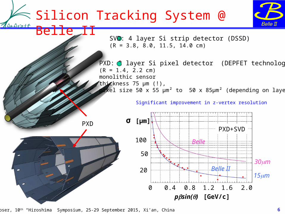
Material Budget (single layer)
12
Belle II
Frame thickness 525 µm
Sensitive layer 75 µm
Switcher thickness
500µm
Cu layer only on periphery
Total 0.21 %X0

H.G. Moser, 10th “Hiroshima” Symposium, 25-29 September 2015, Xi’an, China
Support
13
1) Beam pipe with PXD support (silver)2) End flanges for module mounting and cooling3) Inner layer ladders (2 modules joined back to back)4) Outer layer ladders (2 modules joinded back to back)

H.G. Moser, 10th “Hiroshima” Symposium, 25-29 September 2015, Xi’an, China
Cooling
14
150mW/cm²
CO2 cooling for the electronics outside the detector acceptance (320W)Cold N2 flow to cool sensors and switcher electronics (40W, 150mW/cm²)

H.G. Moser, 10th “Hiroshima” Symposium, 25-29 September 2015, Xi’an, China
Injection Noise & Gating
15
DEPFET frame readout needs 20µs (and covers a time interval of 40 µs)=> Sensor filled with hits from freshly injected bunches => ~ 20% dead time (4ms/20ms)
Gating : Sensor is made blind for a short time during high background (noisy bunch)Signals detected in the clean period before are preserved
Continuous injection with 50 HzEvery 20 ms two bunches are topped up‘cooling’ time: ca 4ms‘noisy’ bunches pass the interaction region every 10µs
In normal clear operation the gate is pulsed negatively(repels electrons)
The clear contact is pulsed positively(attracts electrons from internal gate and bulk underneath)
In gated mode the gate is not pulsed and remains attractive for electrons.
The clear is pulsed positively,and attract electrons from the bulk underneath

H.G. Moser, 10th “Hiroshima” Symposium, 25-29 September 2015, Xi’an, China
Electron drift directions
16
Normal operation:Signal charge drifts into internal gate
Gated ModeCharges from background drift directly to clear gate
Signal already stored in internal gate is protected

H.G. Moser, 10th “Hiroshima” Symposium, 25-29 September 2015, Xi’an, China
Test with laser
17
No clear
clear
Protection of signal charge
Rejection of backround charge

H.G. Moser, 10th “Hiroshima” Symposium, 25-29 September 2015, Xi’an, China
Conclusions & Status
18
The Belle II Detector at SuperKEKB will be equipped with a DEPFET pixel detector
75 µm active silicon thickness, 0.21% X0
Production of 30 wafers with 6 modules each (one inner ladder, two outer ladders)All wafers processed up to metal 13 ‘pilot’ wafers finished (metal 1-3, thinning and cutting)3 modules equipped with ASICs and SMD
This month: tests in the lab and with beam
Completion of 27 remaining wafers in 2016
BEAST II test detector (2 ladders + SVD ladders + rad detectors) in Belle II in 2017
Installation of final PXD detector end of 2017
First physics beam in 2018