Embed Size (px)
Citation preview
LTC4303
14303fb
FEATURES DESCRIPTIO
U
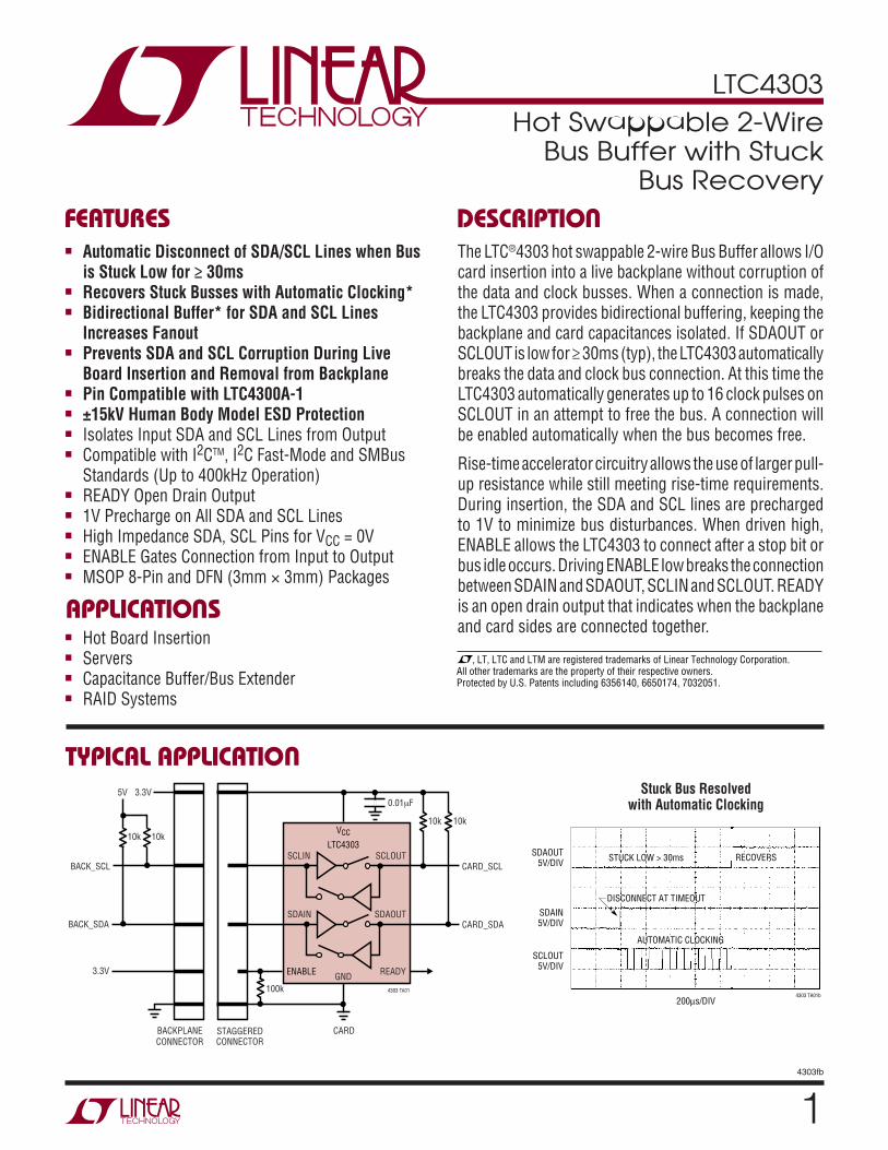
TYPICAL APPLICATIO
U
APPLICATIO SU
10k10k
5V
BACK_SCL
BACKPLANECONNECTOR
CARD
BACK_SDA
3.3V
3.3V
100k
ENABLE
CARD_SCL
CARD_SDA
SCLOUTSCLIN
SDAOUTSDAIN
GND
VCC
LTC4303
READY
0.01F
4303 TA01
10k 10k
STAGGEREDCONNECTOR
, LT, LTC and LTM are registered trademarks of Linear Technology Corporation.All other trademarks are the property of their respective owners. Protected by U.S. Patents including 6356140, 6650174, 7032051.
Hot Swappable 2-Wire Bus Buffer with Stuck
Bus Recovery
The LTC®4303 hot swappable 2-wire Bus Buffer allows I/O card insertion into a live backplane without corruption of the data and clock busses. When a connection is made, the LTC4303 provides bidirectional buffering, keeping the backplane and card capacitances isolated. If SDAOUT or SCLOUT is low for ≥ 30ms (typ), the LTC4303 automatically breaks the data and clock bus connection. At this time the LTC4303 automatically generates up to 16 clock pulses on SCLOUT in an attempt to free the bus. A connection will be enabled automatically when the bus becomes free.
Rise-time accelerator circuitry allows the use of larger pull-up resistance while still meeting rise-time requirements. During insertion, the SDA and SCL lines are precharged to 1V to minimize bus disturbances. When driven high, ENABLE allows the LTC4303 to connect after a stop bit or bus idle occurs. Driving ENABLE low breaks the connection between SDAIN and SDAOUT, SCLIN and SCLOUT. READY is an open drain output that indicates when the backplane and card sides are connected together.
Automatic Disconnect of SDA/SCL Lines when Bus is Stuck Low for ≥ 30ms
Recovers Stuck Busses with Automatic Clocking* Bidirectional Buffer* for SDA and SCL Lines
Increases Fanout Prevents SDA and SCL Corruption During Live
Board Insertion and Removal from Backplane Pin Compatible with LTC4300A-1 ±15kV Human Body Model ESD Protection Isolates Input SDA and SCL Lines from Output Compatible with I2CTM, I2C Fast-Mode and SMBus
Standards (Up to 400kHz Operation) READY Open Drain Output 1V Precharge on All SDA and SCL Lines High Impedance SDA, SCL Pins for VCC = 0V ENABLE Gates Connection from Input to Output MSOP 8-Pin and DFN (3mm × 3mm) Packages
Hot Board Insertion Servers Capacitance Buffer/Bus Extender RAID Systems
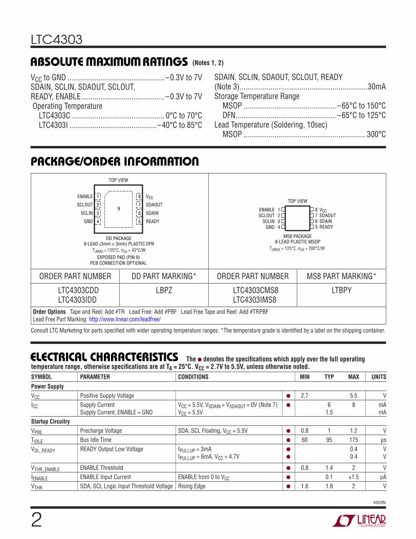
Stuck Bus Resolved with Automatic Clocking
SDAOUT5V/DIV
200s/DIV
STUCK LOW > 30ms
AUTOMATIC CLOCKING
DISCONNECT AT TIMEOUT
RECOVERS
4303 TA01b
SDAIN5V/DIV
SCLOUT5V/DIV
LTC4303
24303fb
ABSOLUTE AXI U RATI GS
W WW U
FOR ATIOPACKAGE/ORDER IU UW
VCC to GND .................................................. –0.3V to 7VSDAIN, SCLIN, SDAOUT, SCLOUT, READY, ENABLE ........................................... –0.3V to 7V Operating Temperature LTC4303C ................................................ 0°C to 70°C LTC4303I .............................................–40°C to 85°C
(Notes 1, 2)
SDAIN, SCLIN, SDAOUT, SCLOUT, READY (Note 3) ..................................................................30mAStorage Temperature Range MSOP ................................................–65°C to 150°C DFN ....................................................–65°C to 125°CLead Temperature (Soldering, 10sec) MSOP ............................................................... 300°C
ELECTRICAL CHARACTERISTICS The denotes the specifi cations which apply over the full operating temperature range, otherwise specifi cations are at TA = 25°C. VCC = 2.7V to 5.5V, unless otherwise noted.SYMBOL PARAMETER CONDITIONS MIN TYP MAX UNITS
Power SupplyVCC Positive Supply Voltage 2.7 5.5 VICC Supply Current VCC = 5.5V, VSDAIN = VSDAOUT = 0V (Note 7) 6 8 mA Supply Current, ENABLE = GND VCC = 5.5V 1.5 mAStartup CircuitryVPRE Precharge Voltage SDA, SCL Floating, VCC = 5.5V 0.8 1 1.2 VTIDLE Bus Idle Time 60 95 175 µsVOL_READY READY Output Low Voltage IPULLUP = 3mA 0.4 V IPULLUP = 6mA, VCC = 4.7V 0.4 V
VTHR_ENABLE ENABLE Threshold 0.8 1.4 2 VIENABLE ENABLE Input Current ENABLE from 0 to VCC 0.1 ±1.5 µAVTHR SDA, SCL Logic Input Threshold Voltage Rising Edge 1.6 1.8 2 V
TJMAX = 125°C, θJA = 200°C/WTJMAX = 125°C, θJA = 43°C/W
TOP VIEW
DD PACKAGE8-LEAD (3mm × 3mm) PLASTIC DFN
5
6
7
8
4
3
2
1ENABLE
SCLOUT
SCLIN
GND
VCC
SDAOUT
SDAIN
READY
EXPOSED PAD (PIN 9)PCB CONNECTION OPTIONAL
9 1234
ENABLESCLOUT
SCLINGND
8765
VCCSDAOUTSDAINREADY
TOP VIEW
MS8 PACKAGE8-LEAD PLASTIC MSOP
ORDER PART NUMBER DD PART MARKING* ORDER PART NUMBER MS8 PART MARKING*
LTC4303CDDLTC4303IDD
LBPZ LTC4303CMS8LTC4303IMS8
LTBPY
Order Options Tape and Reel: Add #TR Lead Free: Add #PBF Lead Free Tape and Reel: Add #TRPBFLead Free Part Marking: http://www.linear.com/leadfree/
Consult LTC Marketing for parts specifi ed with wider operating temperature ranges. *The temperature grade is identifi ed by a label on the shipping container.
LTC4303
34303fb
ELECTRICAL CHARACTERISTICS The denotes the specifi cations which apply over the full operating temperature range, otherwise specifi cations are at TA = 25°C. VCC = 2.7V to 5.5V, unless otherwise noted.
Note 1: Stresses beyond those listed under Absolute Maximum Ratings may cause permanent damage to the device. Exposure to any Absolute Maximum Rating condition for extended periods may affect device reliability and lifetime.Note 2: All currents into pins are positive; all voltages are referenced to GND unless otherwise specifi ed.Note 3: Pulsed less than 5µs.
Note 4: The connection circuitry always regulates the output to a higher voltage than its input. The magnitude of this offset voltage as a function of the pull-up resistor and VCC voltage is shown in the Typical Performance Characteristics section.Note 5: IPULLUPAC varies with temperature and VCC voltage, as shown in the Typical Performance Characteristics section.Note 6: Guaranteed by design, not tested in production.Note 7: ICC test performed with connection circuitry active.
SYMBOL PARAMETER CONDITIONS MIN TYP MAX UNITS
VHYS SDA, SCL, Logic Input Threshold Voltage (Note 6) 50 mV Hysteresis tPHL_ENABLE Delay ENABLE High-Low to Disconnect VCC = 3.3V 300 nstPHL_READY Delay READY High-Low after Disconnect 10 nstPLH_ENABLE Delay ENABLE Low-High to Connect VCC = 3.3V 60 95 175 µstPLH_READY Delay READY Low-High after Connect 10 nsIOFF_READY Ready Off Leakage Current ±10 µARise-Time AcceleratorsIPULLUPAC Transient Boosted Pull-Up Current Positive Transition on SDA, SCL, VCC = 2.7V, 2 3.5 5.5 mA Slew Rate = 0.8V/µs (Note 5) Bus Stuck Low TimeouttTIMEOUT Bus Stuck Low Timer SDAOUT, SCLOUT = 0V 25 30 35 msInput-Output ConnectionVOS Input-Output Offset Voltage 10k to VCC on SDA, SCL, 40 80 120 mV 2.7k to VCC on SDA, SCL 50 100 150 mV VCC = 3.3V, VSDA/SCL = 0.2V (Note 4)CIN Digital Input Capacitance (Note 6) 10 pF SDAIN, SDAOUT, SCLIN, SCLOUTVIL, MAX Input Logic Low Voltage 0.4 VILEAK Input Leakage Current SDA, SCL, VCC = 5.5V ±5 µAVOL Output Low Voltage, Input = 0 SDA, SCL Pins, ISINK = 4mA, VCC = 2.7V 0 0.19 0.3 VTiming CharacteristicsfI2C, MAX I2C Maximum Operating Frequency (Note 6) 400 600 kHztBUF Bus Free Time Between Stop and Start (Note 6) 1.3 µs ConditiontHD, STA Hold Time After (Repeated) (Note 6) 100 ns Start ConditiontSU, STA Repeated Start Condition Set-Up Time (Note 6) 0 nstSU, STO Stop Condition Set-Up Time (Note 6) 0 nstHD, DATI Data Hold Time Input (Note 6) 0 nstSU, DAT Data Set-Up Time (Note 6) 100 ns
LTC4303
44303fb
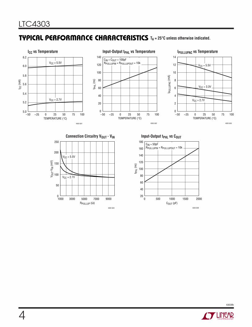
–50 –25 0 25 50 75 100TEMPERATURE (°C)
t PHL
(ns)
140
120
100
80
60
40
20
0
4303 G02
–50 –25 0 25 50 75 100–50 –25 0 25 50 75 100TEMPERATURE (°C)
I PUL
LUPA
C (m
A)
14
12
10
8
6
4
2
0
4303 G03
RPULLUP (Ω)10000
V OUT
-VIN
(mV)
50
150
200
250
3000 5000
4303 G04
100
7000 9000COUT (pF)
0
t PHL
(ns)
1500
4303 G05
500 1000 2000
180
160
140
120
100
80
60
40
20
VCC = 5.5V
VCC = 2.7V
VCC = 5.5V
VCC = 3.3V
VCC = 2.7V
CIN = COUT = 100pFRPULLUPIN = RPULLUPOUT = 10k
CIN = 50pFRPULLUPIN = RPULLUPOUT = 10k
TEMPERATURE (°C)
5.0
I CC
(mA)
5.4
5.8
6.2
5.2
5.6
6.0
4303 G01
VCC = 5.5V
VCC = 2.7V
TYPICAL PERFOR
UW
CE CHARACTERISTICSA
ICC vs Temperature Input-Output tPHL vs Temperature IPULLUPAC vs Temperature
Input-Output tPHL vs COUTConnection Circuitry VOUT - VIN
TA = 25°C unless otherwise indicated.
LTC4303
54303fb
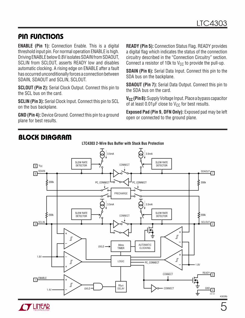
PI FU CTIO S
UUU
BLOCK DIAGRA
W
ENABLE (Pin 1): Connection Enable. This is a digital threshold input pin. For normal operation ENABLE is high. Driving ENABLE below 0.8V isolates SDAIN from SDAOUT, SCLIN from SCLOUT, asserts READY low and disables automatic clocking. A rising edge on ENABLE after a fault has occurred unconditionally forces a connection between SDAIN, SDAOUT and SCLIN, SCLOUT.
SCLOUT (Pin 2): Serial Clock Output. Connect this pin to the SCL bus on the card.
SCLIN (Pin 3): Serial Clock Input. Connect this pin to SCL on the bus backplane.
GND (Pin 4): Device Ground. Connect this pin to a ground plane for best results.
READY (Pin 5): Connection Status Flag. READY provides a digital fl ag which indicates the status of the connection circuitry described in the “Connection Circuitry” section. Connect a resistor of 10k to VCC to provide the pull-up.
SDAIN (Pin 6): Serial Data Input. Connect this pin to the SDA bus on the backplane.
SDAOUT (Pin 7): Serial Data Output. Connect this pin to the SDA bus on the card.
VCC (Pin 8): Supply Voltage Input. Place a bypass capacitor of at least 0.01µF close to VCC for best results.
Exposed Pad (Pin 9, DFN Only): Exposed pad may be left open or connected to the ground plane.
LTC4303 2-Wire Bus Buffer with Stuck Bus Protection
CONNECT
PC_CONNECT PC_CONNECT
PC_CONNECT
CONNECT
1
200k
200k
200k
200k
PRECHARGE
LOGIC
30msTIMER
95sDELAY1.4V
ENABLE
1.8V
3SCLIN
6SDAIN
1.8V
CONNECT
CONNECT
7SDAOUT
8 VCC
2SCLOUT
READY5
GND
4301 BD
4
SLEW RATEDETECTOR
3.5mA
SLEW RATEDETECTOR
3.5mA
SLEW RATEDETECTOR
3.5mA
SLEW RATEDETECTOR
3.5mA
UVLO
UVLO
–
+
–
+
–
+–
+
–
+
AUTOMATICCLOCKING
LTC4303
64303fb
Start-Up
When the LTC4303 fi rst receives power on its VCC pin, either during power up or live insertion, it starts in an under voltage lockout (UVLO) state, ignoring any activity on the SDA or SCL pins until VCC rises above 2.5V (typical).
During this time, the precharge circuitry is active and forces 1V through 200k nominal resistors to the SDA and SCL pins. Because the I/O card is being plugged into a live backplane, the voltage on the backplane SDA and SCL busses may be anywhere between 0V and VCC. Precharging the SCL and SDA pins to 1V minimizes the worst-case voltage differential these pins will see at the moment of connection, therefore minimizing the amount of disturbance caused by the I/O card.
Once the LTC4303 comes out of UVLO, it assumes that SDAIN and SCLIN have been inserted into a live system and that SDAOUT and SCLOUT are being powered up at the same time as itself. Therefore, it looks for either a stop bit or bus idle condition on the input side to indicate the completion of a data transaction. When either one occurs, the part also verifi es that both the SDAOUT and SCLOUT voltages are high. When all of these conditions are met, the input-to-output connection circuitry is activated, join-ing the SDA and SCL busses on the I/O card with those on the backplane and READY goes high.
Connection Circuitry
Once the connection circuitry is activated, the functionality of the SDAIN and SDAOUT pins is identical. A low forced on either pin at any time results in both pin voltages be-ing low. For proper operation, logic low input voltages should be no higher than 0.4V with respect to the ground pin voltage of the LTC4303. SDAIN and SDAOUT enter a logic high state only when all devices on both SDAIN and SDAOUT release high. The same is true for SCLIN and SCLOUT. This important feature ensures that clock stretching, clock synchronization, arbitration and the ac-knowledge protocol always work, regardless of how the devices in the system are tied to the LTC4303.
Another key feature of the connection circuitry is that it provides bidirectional buffering, keeping the backplane and card capacitances isolated. Because of this isolation,
OPERATIOU
the waveforms on the backplane busses look slightly different than the corresponding card bus waveforms, as described here.
Input to Output Offset Voltage
When a logic low voltage, VLOW1, is driven on any of the LTC4303’s data or clock pins, the LTC4303 regulates the voltage on the opposite side of the part (call it VLOW2) to a slightly higher voltage, as directed by the following equation:
VLOW2 = VLOW1 + 75mV + (VCC/R) • 20Ω (typical)
where R is the bus pull-up resistance in ohms. For ex-ample, if a device is forcing SDAOUT to 10mV where VCC = 3.3V and the pull-up resistor R on SDAIN is 10k, then the voltage on SDAIN = 10mV + 75mV + (3.3/10000) • 20 = 91.6mV (typical). See the Typical Performance Characteristics section for curves showing the offset voltage as a function of VCC and R.
Bus Stuck Low Time-Out
When SDAOUT or SCLOUT is low, an internal timer starts. The timer is only reset when SDAOUT and SCLOUT are both high. If they do not go high within 30ms (typical), the connection between SDAIN and SDAOUT, and SCLIN and SCLOUT is broken. After a delay of at least 40µs the LTC4303 automatically generates up to 16 clock pulses at 8.5kHz (typical) on SCLOUT in an attempt to unstick the bus. When SDAOUT and SCLOUT go high, reconnection occurs when the conditions described in the “Start-Up” section above are satisfi ed.
When powering up into a bus stuck low condition, the connection circuitry joining the SDA and SCL busses on the I/O card with those on the backplane is not activated. 30ms after UVLO, automatic clocking takes place as described above.
Propagation Delays
During a rising edge, the rise-time on each side is de-termined by the bus pull-up resistor and the equivalent capacitance on the line. If the pull-up resistors are the same, a difference in rise-time occurs which is directly proportional to the difference in capacitance between
LTC4303
74303fb
OUTPUT SIDE50pF
0.5V/DIV
INPUT SIDE150pF0.5V/DIV
200ns/DIV4303 F01
INPUT SIDE50pF
0.5V/DIV
OUTPUT SIDE150pF0.5V/DIV
20ns/DIV4303 F02
OPERATIOU
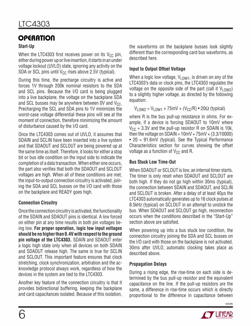
Figure 1. Input-Output Connection tPLH
the two sides. This effect is displayed in Figure 1 for a VCC = 3.3V and a 10k pull-up resistor on each side (50pF on one side and 150pF on the other). Since the output side has less capacitance than the input, it rises faster and the effective tPLH is negative.
There is a propagation delay, tPHL, through the connec-tion circuitry for falling waveforms. Figure 2 shows the falling edge waveforms. An external driver pulls down the voltage on the side with 50pF capacitance; LTC4303 pulls down the voltage on the opposite side with a delay of 80ns. This delay is always positive and is a function of supply voltage, temperature and the pull-up resistors and equivalent bus capacitances on both sides of the bus. The Typical Performance Characteristics section shows tPHL as a function of temperature and voltage for 10k pull-up resistors and 100pF equivalent capacitance on both sides of the part. Larger output capacitances translate to longer delays. Users must quantify the difference in propagation times for a rising edge versus a falling edge in their systems and adjust setup and hold times accordingly.
READY Digital Output
The READY pin provides a digital fl ag which indicates the status of the connection circuitry described previously in the “Connection Circuitry” section. READY is high when the connection circuitry is active, and pulls low when there is not a valid connection. The pin is driven by an open drain pull-down capable of sinking 3mA while hold-ing 0.4V on the pin. Connect a resistor of 10k to VCC to provide the pull-up.
ENABLE
When the ENABLE pin is driven below 0.8V with respect to the LTC4303’s ground, the backplane side is discon-nected from the card side, and the READY pin is internally pulled low. When the pin is driven above 2V, the part waits for data transactions on the IN side to be complete and for the OUT side to be high (as described in the Start-Up section) before connecting the two sides. At this time the internal pull-down on READY releases. When ENABLE is low, automatic clocking is disabled.
A rising edge on ENABLE after a stuck bus condition has occurred forces a connection between SDAIN, SDAOUT and SCLIN, SCLOUT even if bus idle conditions are not met. At this time the internal 30ms timer is reset but not disabled.
Rise Time Accelerators
Once connection has been established, rise time accelerator circuits on all four SDA and SCL pins are activated. These allow the use of larger pull-up resistors, reducing power consumption, or bus capacitance beyond that specifi ed in I2C, while still meeting system rise time requirements. During positive bus transitions, the LTC4303 switches in 3.5mA (typical) of current to quickly slew the SDA and SCL lines once their DC voltages exceed 0.8V. Choose a pull-up resistor so that the bus will rise on its own at a rate of at least 0.8V/µs to guarantee activation of the ac-celerators. Rise time accelerators turn off when SDA and SCL lines are approximately 1V below VCC.The rise time accelerators are automatically disabled during automatic clocking.
Figure 2. Input-Output Connection tPHL
LTC4303
84303fb
Resistor Pull-Up Selection
The system pull-up resistors must be strong enough to provide a positive slew rate of 0.8V/µs on the SDA and SCL pins, in order to activate the rise time accelera-tors during rising edges. Choose maximum resistor value RPULL-UP(MAX) using the formula:
where VBUSMIN is the minimum operating pull-up sup-ply voltage, and CBUS the total capacitance on respec-tive bus line.
R k
V V ns V
C pFPULLUP MAXBUS MIN
BUS( )
( )[ ]– . • [ / ]
[ ]Ω =
( )0 8 1250
For example, assume VBUS = VCC = 3.3V, and assuming ±10% supply tolerance, VBUSMIN = 2.97V. With CBUS = 100pF, RPULL-UP, MAX = 27.1k. Therefore a smaller pull-up resistor than 27.1k must be used, so 10k works fi ne.
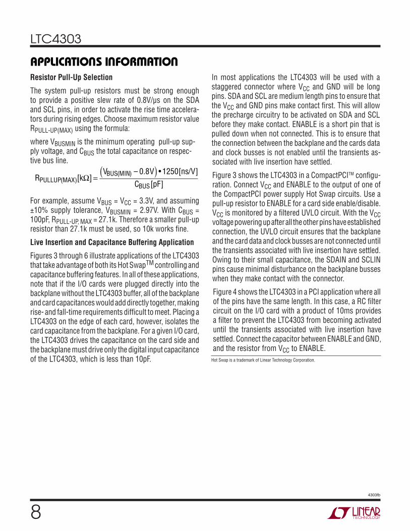
Live Insertion and Capacitance Buffering Application
Figures 3 through 6 illustrate applications of the LTC4303 that take advantage of both its Hot SwapTM controlling and capacitance buffering features. In all of these applications, note that if the I/O cards were plugged directly into the backplane without the LTC4303 buffer, all of the backplane and card capacitances would add directly together, making rise- and fall-time requirements diffi cult to meet. Placing a LTC4303 on the edge of each card, however, isolates the card capacitance from the backplane. For a given I/O card, the LTC4303 drives the capacitance on the card side and the backplane must drive only the digital input capacitance of the LTC4303, which is less than 10pF.
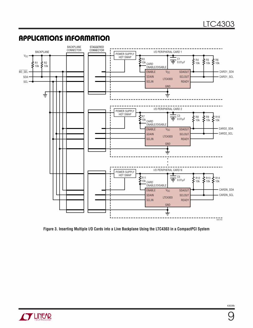
In most applications the LTC4303 will be used with a staggered connector where VCC and GND will be long pins. SDA and SCL are medium length pins to ensure that the VCC and GND pins make contact fi rst. This will allow the precharge circuitry to be activated on SDA and SCL before they make contact. ENABLE is a short pin that is pulled down when not connected. This is to ensure that the connection between the backplane and the cards data and clock busses is not enabled until the transients as-sociated with live insertion have settled.
Figure 3 shows the LTC4303 in a CompactPCITM confi gu-ration. Connect VCC and ENABLE to the output of one of the CompactPCI power supply Hot Swap circuits. Use a pull-up resistor to ENABLE for a card side enable/disable. VCC is monitored by a fi ltered UVLO circuit. With the VCC voltage powering up after all the other pins have established connection, the UVLO circuit ensures that the backplane and the card data and clock busses are not connected until the transients associated with live insertion have settled. Owing to their small capacitance, the SDAIN and SCLIN pins cause minimal disturbance on the backplane busses when they make contact with the connector.
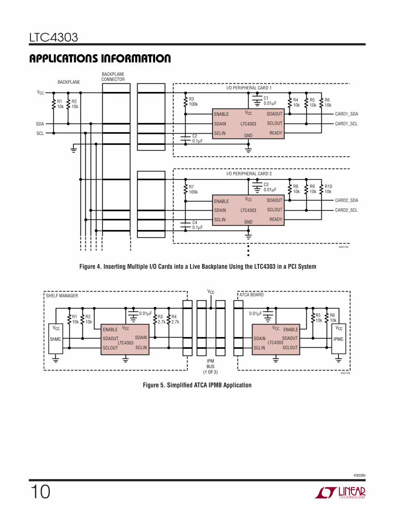
Figure 4 shows the LTC4303 in a PCI application where all of the pins have the same length. In this case, a RC fi lter circuit on the I/O card with a product of 10ms provides a fi lter to prevent the LTC4303 from becoming activated until the transients associated with live insertion have settled. Connect the capacitor between ENABLE and GND, and the resistor from VCC to ENABLE.
Hot Swap is a trademark of Linear Technology Corporation.
APPLICATIO S I FOR ATIO
WU UU
LTC4303
94303fb
APPLICATIO S I FOR ATIO
WU UU
Figure 3. Inserting Multiple I/O Cards into a Live Backplane Using the LTC4303 in a CompactPCI System
R1310k
R1210k
R1410k
I/O PERIPHERAL CARD N
CARDN_SCL
CARDN_SDA
4303 F03
• • •
R910k
R810k
R1010k
I/O PERIPHERAL CARD 2
CARD2_SCL
CARD2_SDA
R510k
R410k
R610k
I/O PERIPHERAL CARD 1
CARD1_SCL
CARD1_SDA
R110k
VCC
R210k
BACKPLANE
BACKPLANECONNECTOR
CARDENABLE/DISABLE
SDA
BD_SEL
SCL
C10.01µF
R310k
R710k
R1110k
C30.01µF
C50.01µF
POWER SUPPLYHOT SWAP
POWER SUPPLYHOT SWAP
POWER SUPPLYHOT SWAP
CARDENABLE/DISABLE
CARDENABLE/DISABLE
ENABLE
SDAIN
SCLIN
VCC
GND
SDAOUT
SCLOUT
READYLTC4303
ENABLE
SDAIN
SCLIN
VCC
GND
SDAOUT
SCLOUT
READYLTC4303
ENABLE
SDAIN
SCLIN
VCC
GND
SDAOUT
SCLOUT
READYLTC4303
STAGGEREDCONNECTOR
LTC4303
104303fb
S I FOR ATIOAPPLICATIO
WU UU
Figure 4. Inserting Multiple I/O Cards into a Live Backplane Using the LTC4303 in a PCI System
Figure 5. Simplifi ed ATCA IPMB Application
R3100k
SDAIN
SCLIN
VCC
GND
SDAOUT
SCLOUT
READY
ENABLE
SDAIN
SCLIN
VCC
GND
SDAOUT
SCLOUT
READY
4303 F04
R910k
R810k
R1010k
I/O PERIPHERAL CARD 2
LTC4303 CARD2_SCL
CARD2_SDA
R510k
R410k
I/O PERIPHERAL CARD 1
LTC4303 CARD1_SCL
CARD1_SDA
R110k
VCC
R210k
BACKPLANE
BACKPLANECONNECTOR
SDA
SCL
C10.01F
C20.1F
C30.01F
R610k
•••
R7100k
ENABLE
C40.1F
SDAIN
SCLIN
SDAOUT
SCLOUT
ENABLE VCC
R110k
R210k
R32.7k
0.01µFR42.7k
R510k
R610k
LTC4303SDAOUT
SCLOUT
SDAIN
SCLIN
ENABLEVCC
LTC4303
4303 F05
VCC
VCC
ShMC
VCC
IPMC
IPMBUS
(1 OF 2)
SHELF MANAGER ATCA BOARD
0.01µF
LTC4303
114303fb
PACKAGE DESCRIPTIO
U
3.00 ±0.10(4 SIDES)
NOTE:1. DRAWING TO BE MADE A JEDEC PACKAGE OUTLINE M0-229 VARIATION OF (WEED-1)2. DRAWING NOT TO SCALE3. ALL DIMENSIONS ARE IN MILLIMETERS4. DIMENSIONS OF EXPOSED PAD ON BOTTOM OF PACKAGE DO NOT INCLUDE MOLD FLASH. MOLD FLASH, IF PRESENT, SHALL NOT EXCEED 0.15mm ON ANY SIDE5. EXPOSED PAD SHALL BE SOLDER PLATED6. SHADED AREA IS ONLY A REFERENCE FOR PIN 1 LOCATION
ON TOP AND BOTTOM OF PACKAGE
0.38 ± 0.10
BOTTOM VIEW—EXPOSED PAD
1.65 ± 0.10(2 SIDES)
0.75 ±0.05
R = 0.115TYP
2.38 ±0.10(2 SIDES)
14
85
PIN 1TOP MARK
(NOTE 6)
0.200 REF
0.00 – 0.05
(DD8) DFN 1203
0.25 ± 0.05
2.38 ±0.05(2 SIDES)
RECOMMENDED SOLDER PAD PITCH AND DIMENSIONS
1.65 ±0.05(2 SIDES)2.15 ±0.05
0.50BSC
0.675 ±0.05
3.5 ±0.05
PACKAGEOUTLINE
0.25 ± 0.050.50 BSC
MSOP (MS8) 0204
0.53 ± 0.152(.021 ± .006)
SEATINGPLANENOTE:
1. DIMENSIONS IN MILLIMETER/(INCH)2. DRAWING NOT TO SCALE3. DIMENSION DOES NOT INCLUDE MOLD FLASH, PROTRUSIONS OR GATE BURRS. MOLD FLASH, PROTRUSIONS OR GATE BURRS SHALL NOT EXCEED 0.152mm (.006") PER SIDE4. DIMENSION DOES NOT INCLUDE INTERLEAD FLASH OR PROTRUSIONS. INTERLEAD FLASH OR PROTRUSIONS SHALL NOT EXCEED 0.152mm (.006") PER SIDE5. LEAD COPLANARITY (BOTTOM OF LEADS AFTER FORMING) SHALL BE 0.102mm (.004") MAX
0.18(.007)
0.254(.010)
1.10(.043)MAX
0.22 – 0.38(.009 – .015)
TYP
0.127 ± 0.076(.005 ± .003)
0.86(.034)REF
0.65(.0256)
BSC
0° – 6° TYP
DETAIL “A”
DETAIL “A”
GAUGE PLANE
1 2 3 4
4.90 ± 0.152(.193 ± .006)
8 7 6 5
3.00 ± 0.102(.118 ± .004)
(NOTE 3)
3.00 ± 0.102(.118 ± .004)
(NOTE 4)
0.52(.0205)
REF
5.23(.206)MIN
3.20 – 3.45(.126 – .136)
0.889 ± 0.127(.035 ± .005)
RECOMMENDED SOLDER PAD LAYOUT
0.42 ± 0.038(.0165 ± .0015)
TYP
0.65(.0256)
BSC
MS8 Package8-Lead Plastic MSOP
(Reference LTC DWG # 05-08-1660)
DD Package8-Lead Plastic DFN (3mm × 3mm)(Reference LTC DWG # 05-08-1698)
Information furnished by Linear Technology Corporation is believed to be accurate and reliable.However, no responsibility is assumed for its use. Linear Technology Corporation makes no represen-tation that the interconnection of its circuits as described herein will not infringe on existing patent rights.
LTC4303
124303fb
Linear Technology Corporation1630 McCarthy Blvd., Milpitas, CA 95035-7417 (408) 432-1900 FAX: (408) 434-0507 www.linear.com © LINEAR TECHNOLOGY CORPORATION 2005
LT/LWI 0806 REV B • PRINTED IN USA
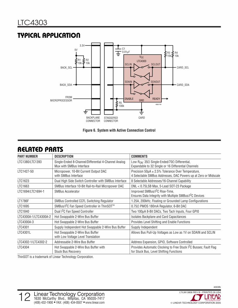
TYPICAL APPLICATIO
U
Figure 6. System with Active Connection Control
RELATED PARTS
CARD
FROMMICROPROCESSOR
ENABLE
CARD_SCL
CARD_SDA
SCLOUTSCLIN
SDAOUTSDAIN
GND
VCC
LTC4303
READY
C10.01F
4303 F06
R110k
R210k
R310k
R410k
R5100k
5V
BACK_SCL
BACKPLANECONNECTOR
BACK_SDA
3.3V
STAGGEREDCONNECTOR
PART NUMBER DESCRIPTION COMMENTS
LTC1380/LTC1393 Single-Ended 8-Channel/Differential 4-Channel Analog Low RON: 35Ω Single-Ended/70Ω Differential, Mux with SMBus Interface Expandable to 32 Single or 16 Differential ChannelsLTC1427-50 Micropower, 10-Bit Current Output DAC Precision 50µA ± 2.5% Tolerance Over Temperature, with SMBus Interface 4 Selectable SMBus Addresses, DAC Powers up at Zero or MidscaleLTC1623 Dual High Side Switch Controller with SMBus Interface 8 Selectable Addresses/16-Channel Capability LTC1663 SMBus Interface 10-Bit Rail-to-Rail Micropower DAC DNL < 0.75LSB Max, 5-Lead SOT-23 PackageLTC1694/LTC1694-1 SMBus Accelerator Improved SMBus/I2C Rise-Time, Ensures Data Integrity with Multiple SMBus/I2C Devices LT1786F SMBus Controlled CCFL Switching Regulator 1.25A, 200kHz, Floating or Grounded Lamp Confi gurationsLTC1695 SMBus/I2C Fan Speed Controller in ThinSOTTM 0.75Ω PMOS 180mA Regulator, 6-Bit DACLTC1840 Dual I2C Fan Speed Controller Two 100µA 8-Bit DACs, Two Tach Inputs, Four GPI0LTC4300A-1/LTC4300A-2 Hot Swappable 2-Wire Bus Buffer Isolates Backplane and Card CapacitancesLTC4300A-3 Hot Swappable 2-Wire Bus Buffer Provides Level Shifting and Enable Functions LTC4301 Supply Independent Hot Swappable 2-Wire Bus Buffer Supply IndependentLTC4301L Hot Swappable 2-Wire Bus Buffer Allows Bus Pull-Up Voltages as Low as 1V on SDAIN and SCLIN with Low Voltage Level TranslationLTC4302-1/LTC4302-2 Addressable 2-Wire Bus Buffer Address Expansion, GPIO, Software ControlledLTC4304 Hot Swappable 2-Wire Bus Buffer with Provides Automatic Clocking to Free Stuck I2C Busses; Fault Flag Stuck Bus Recovery for Stuck Bus, Level Shifting FunctionsThinSOT is a trademark of Linear Technology Corporation.


![Cranial MR Imaging in Neurofibromatosis · bromatosis), neurofibromatosis II (bilateral acoustic neurofibromatosis), and other forms [5, 6]. Neuroradiology has traditionally played](https://img.pdfslide.net/doc/110x75/5ed593375be95c6187174771/cranial-mr-imaging-in-bromatosis-neurofibromatosis-ii-bilateral-acoustic-neurofibromatosis.jpg)