Embed Size (px)
Citation preview
Chapter 32. Physical Optics and Electronics
32-1
Physical Optics and Electronics Academic Staff Professor Rajeev J. Ram, Dr. Harry Lee Research Staff and Visiting Scientists Dr. Harry Lee, Mariana Fernandes (MIT Portugal Program), Eugen Zgraggen (ETH Zurich) Graduate Students Reja Amatya, Shireen Goh, Evelyn Kapusta, Kevin Lee, Jason Orcutt, Parthi Santhanam Undergraduate Students Amrita Masurkar, Krishna Settaluri Technical and Support Staff Catherine Bourgeois Overview The research in the Physical Optics and Electronics Group is divided along three primary themes:
• Integrated Photonics • Biophotonics and Bioprocessors • Thermodynamics of Semiconductor Devices
In all three areas the goal of this research is to exploit physics to invent new devices that lead to better systems. Each researcher works to model and design a new device, implement the design, and then integrate this device into a system which defines the state-of-the-art. The major achievements of the laboratory during the last year were:
1. Demonstration of photonic devices in a 32nm scaled-CMOS process. 2. Demonstration of microbioreactors in a hybrid-plastic device. 3. Field demonstration of solar thermoelectric generator offering a lower cost alternative to
photovoltaic technology.
Chapter 32. Physical Optics and Electronics
32-2 RLE Progress Report 151
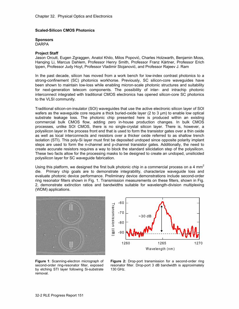
Scaled-Silicon CMOS Photonics Sponsors DARPA Project Staff Jason Orcutt, Eugen Zgraggen, Anatol Khilo, Milos Popović, Charles Holzwarth, Benjamin Moss, Hanqing Li, Marcus Dahlem, Professor Henry Smith, Professor Franz Kärtner, Professor Erich Ippen, Professor Judy Hoyt, Professor Vladimir Stojanović, and Professor Rajeev J. Ram In the past decade, silicon has moved from a work bench for low-index contrast photonics to a strong-confinement (SC) photonics workhorse. Previously, SC silicon-core waveguides have been shown to maintain low-loss while enabling micron-scale photonic structures and suitability for next-generation telecom components. The possibility of inter- and intrachip photonic interconnect integrated with traditional CMOS electronics has opened silicon-core SC photonics to the VLSI community. Traditional silicon-on-insulator (SOI) waveguides that use the active electronic silicon layer of SOI wafers as the waveguide core require a thick buried-oxide layer (2 to 3 µm) to enable low optical substrate leakage loss. The photonic chip presented here is produced within an existing commercial bulk CMOS flow, adding zero in-house production changes. In bulk CMOS processes, unlike SOI CMOS, there is no single-crystal silicon layer. There is, however, a polysilicon layer in the process front end that is used to form the transistor gates over a thin oxide as well as local interconnects and resistors over a thicker oxide referred to as shallow trench isolation (STI). This poly-Si layer must first be deposited undoped since opposite polarity implant steps are used to form the n-channel and p-channel transistor gates. Additionally, the need to create accurate resistors requires a way to block the standard silicidation step of the polysilicon. These two facts allow for the processing masks to be designed to create an undoped, unsilicided polysilicon layer for SC waveguide fabrication. Using this platform, we designed the first bulk photonic chip in a commercial process on a 4 mm2 die. Primary chip goals are to demonstrate integrability, characterize waveguide loss and evaluate photonic device performance. Preliminary device demonstrations include second-order ring resonator filters shown in Fig. 1. Transmission measurements on these filters, shown in Fig. 2, demonstrate extinction ratios and bandwidths suitable for wavelength-division multiplexing (WDM) applications.
Figure 1: Scanning-electron micrograph of second-order ring-resonator filter, exposed by etching STI layer following Si-substrate removal.
Figure 2: Drop-port transmission for a second-order ring resonator filter. Drop-port 3 dB bandwidth is approximately 130 GHz.
Chapter 32. Physical Optics and Electronics
32-3
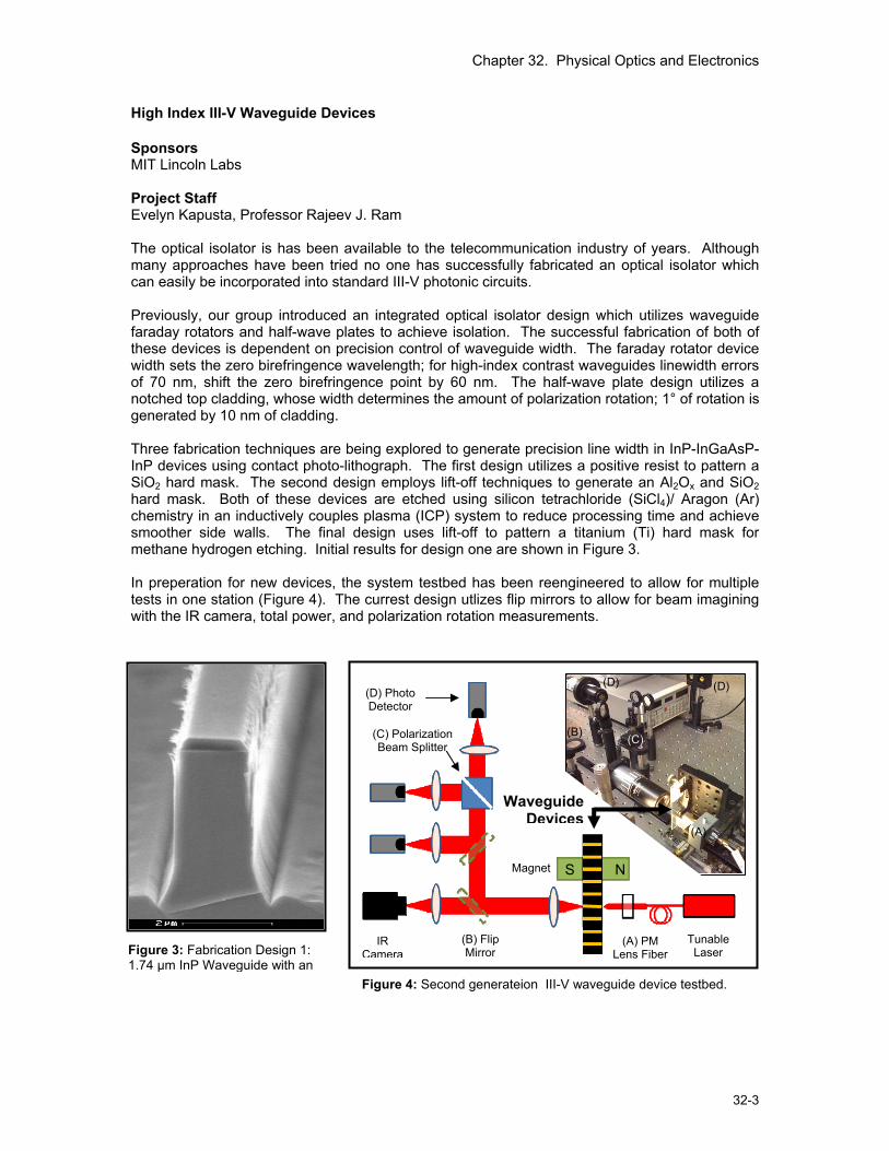
High Index III-V Waveguide Devices Sponsors MIT Lincoln Labs Project Staff Evelyn Kapusta, Professor Rajeev J. Ram The optical isolator is has been available to the telecommunication industry of years. Although many approaches have been tried no one has successfully fabricated an optical isolator which can easily be incorporated into standard III-V photonic circuits. Previously, our group introduced an integrated optical isolator design which utilizes waveguide faraday rotators and half-wave plates to achieve isolation. The successful fabrication of both of these devices is dependent on precision control of waveguide width. The faraday rotator device width sets the zero birefringence wavelength; for high-index contrast waveguides linewidth errors of 70 nm, shift the zero birefringence point by 60 nm. The half-wave plate design utilizes a notched top cladding, whose width determines the amount of polarization rotation; 1° of rotation is generated by 10 nm of cladding. Three fabrication techniques are being explored to generate precision line width in InP-InGaAsP-InP devices using contact photo-lithograph. The first design utilizes a positive resist to pattern a SiO2 hard mask. The second design employs lift-off techniques to generate an Al2Ox and SiO2 hard mask. Both of these devices are etched using silicon tetrachloride (SiCl4)/ Aragon (Ar) chemistry in an inductively couples plasma (ICP) system to reduce processing time and achieve smoother side walls. The final design uses lift-off to pattern a titanium (Ti) hard mask for methane hydrogen etching. Initial results for design one are shown in Figure 3. In preperation for new devices, the system testbed has been reengineered to allow for multiple tests in one station (Figure 4). The currest design utlizes flip mirrors to allow for beam imagining with the IR camera, total power, and polarization rotation measurements.
Figure 3: Fabrication Design 1: 1.74 μm InP Waveguide with an
Figure 4: Second generateion III-V waveguide device testbed.
S N Magnet
Tunable Laser
(D) Photo Detector
(C) Polarization Beam Splitter
(A) PM Lens Fiber
(A)
(C)
(D)
Waveguide Devices
(D)
(B)
(B) Flip Mirror
IR Camera
Chapter 32. Physical Optics and Electronics
32-4 RLE Progress Report 151
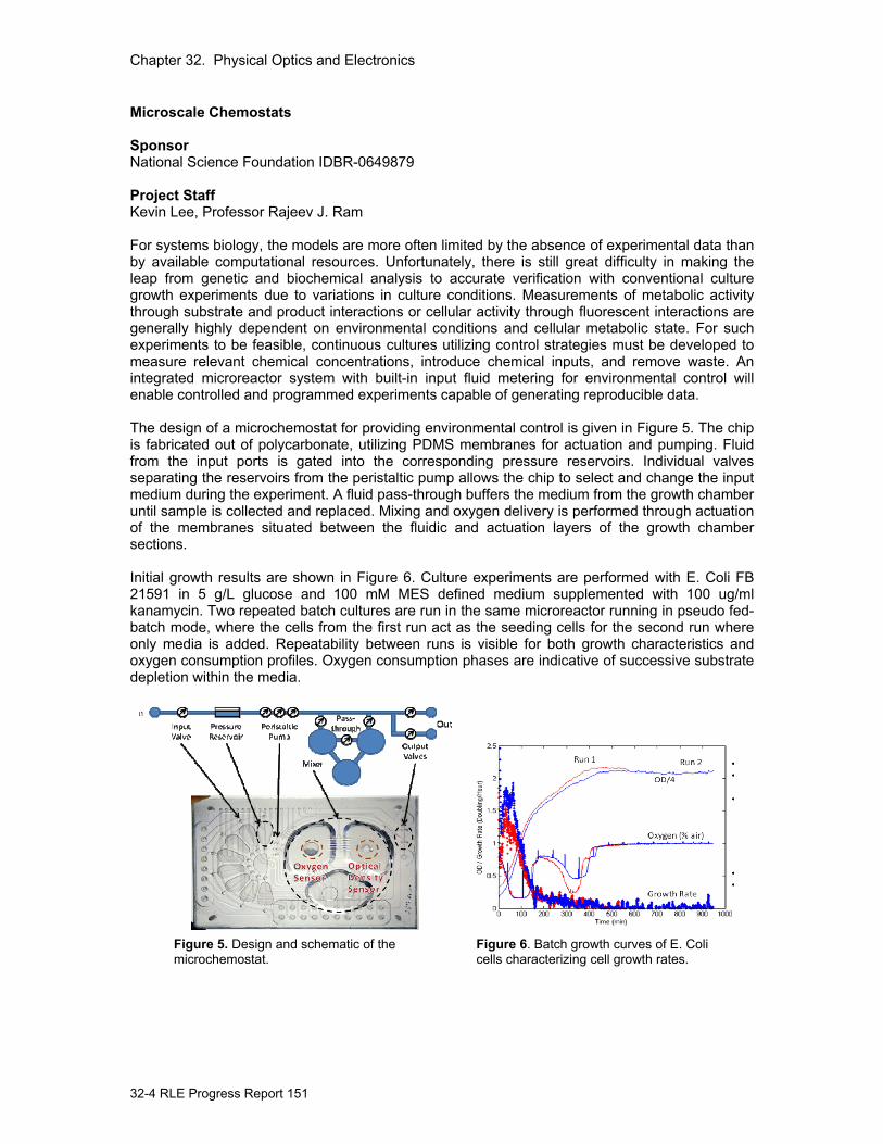
Microscale Chemostats Sponsor National Science Foundation IDBR-0649879 Project Staff Kevin Lee, Professor Rajeev J. Ram For systems biology, the models are more often limited by the absence of experimental data than by available computational resources. Unfortunately, there is still great difficulty in making the leap from genetic and biochemical analysis to accurate verification with conventional culture growth experiments due to variations in culture conditions. Measurements of metabolic activity through substrate and product interactions or cellular activity through fluorescent interactions are generally highly dependent on environmental conditions and cellular metabolic state. For such experiments to be feasible, continuous cultures utilizing control strategies must be developed to measure relevant chemical concentrations, introduce chemical inputs, and remove waste. An integrated microreactor system with built-in input fluid metering for environmental control will enable controlled and programmed experiments capable of generating reproducible data. The design of a microchemostat for providing environmental control is given in Figure 5. The chip is fabricated out of polycarbonate, utilizing PDMS membranes for actuation and pumping. Fluid from the input ports is gated into the corresponding pressure reservoirs. Individual valves separating the reservoirs from the peristaltic pump allows the chip to select and change the input medium during the experiment. A fluid pass-through buffers the medium from the growth chamber until sample is collected and replaced. Mixing and oxygen delivery is performed through actuation of the membranes situated between the fluidic and actuation layers of the growth chamber sections. Initial growth results are shown in Figure 6. Culture experiments are performed with E. Coli FB 21591 in 5 g/L glucose and 100 mM MES defined medium supplemented with 100 ug/ml kanamycin. Two repeated batch cultures are run in the same microreactor running in pseudo fed-batch mode, where the cells from the first run act as the seeding cells for the second run where only media is added. Repeatability between runs is visible for both growth characteristics and oxygen consumption profiles. Oxygen consumption phases are indicative of successive substrate depletion within the media.
Figure 5. Design and schematic of the microchemostat.
Figure 6. Batch growth curves of E. Coli cells characterizing cell growth rates.
Chapter 32. Physical Optics and Electronics
32-5
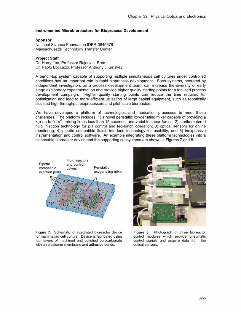
Instrumented Microbioreactors for Bioprocess Development Sponsor National Science Foundation IDBR-0649879 Massachusetts Technology Transfer Center Project Staff Dr. Harry Lee, Professor Rajeev J. Ram Dr. Paolo Boccazzi, Professor Anthony J. Sinskey A bench-top system capable of supporting multiple simultaneous cell cultures under controlled conditions has an important role in rapid bioprocess development. Such systems, operated by independent investigators on a process development team, can increase the diversity of early stage exploratory experimentation and provide higher quality starting points for a focused process development campaign. Higher quality starting points can reduce the time required for optimization and lead to more efficient utilization of large capital equipment, such as robotically assisted high-throughput bioprocessors and pilot-scale bioreactors. We have developed a platform of technologies and fabrication processes to meet these challenges. The platform includes: 1) a novel peristaltic oxygenating mixer capable of providing a kLa up to 0.1s-1, mixing times less than 15 seconds, and variable shear forces; 2) sterile metered fluid injection technology for pH control and fed-batch operation; 3) optical sensors for online monitoring; 4) pipette compatible fluidic interface technology for usability; and 5) inexpensive instrumentation and control software. An example integrating these platform technologies into a disposable bioreactor device and the supporting subsystems are shown in Figures 7 and 8.
Figure 7. Schematic of integrated bioreactor device for mammalian cell culture. Device is fabricated using four layers of machined and polished polycarbonate with an elastomer membrane and adhesive bonds.
Figure 8. Photograph of three bioreactor control modules which provide pneumatic control signals and acquire data from the optical sensors.
Pipette compatible injection ports
Peristaltic oxygenating mixer
Fluid injectors and control valves
Chapter 32. Physical Optics and Electronics
32-6 RLE Progress Report 151
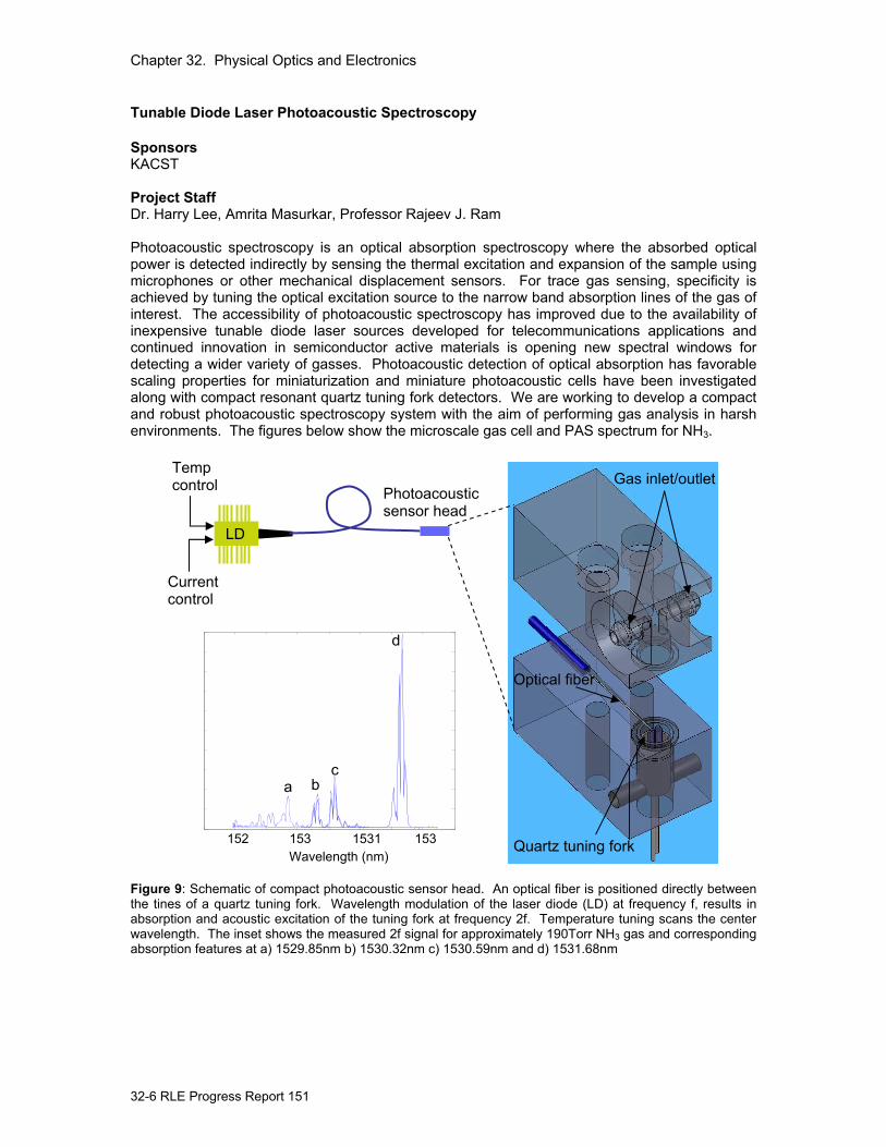
Tunable Diode Laser Photoacoustic Spectroscopy Sponsors KACST Project Staff Dr. Harry Lee, Amrita Masurkar, Professor Rajeev J. Ram Photoacoustic spectroscopy is an optical absorption spectroscopy where the absorbed optical power is detected indirectly by sensing the thermal excitation and expansion of the sample using microphones or other mechanical displacement sensors. For trace gas sensing, specificity is achieved by tuning the optical excitation source to the narrow band absorption lines of the gas of interest. The accessibility of photoacoustic spectroscopy has improved due to the availability of inexpensive tunable diode laser sources developed for telecommunications applications and continued innovation in semiconductor active materials is opening new spectral windows for detecting a wider variety of gasses. Photoacoustic detection of optical absorption has favorable scaling properties for miniaturization and miniature photoacoustic cells have been investigated along with compact resonant quartz tuning fork detectors. We are working to develop a compact and robust photoacoustic spectroscopy system with the aim of performing gas analysis in harsh environments. The figures below show the microscale gas cell and PAS spectrum for NH3.
Figure 9: Schematic of compact photoacoustic sensor head. An optical fiber is positioned directly between the tines of a quartz tuning fork. Wavelength modulation of the laser diode (LD) at frequency f, results in absorption and acoustic excitation of the tuning fork at frequency 2f. Temperature tuning scans the center wavelength. The inset shows the measured 2f signal for approximately 190Torr NH3 gas and corresponding absorption features at a) 1529.85nm b) 1530.32nm c) 1530.59nm and d) 1531.68nm
Optical fiber
Quartz tuning fork
Gas inlet/outlet Temp control
Current control
LD
Photoacoustic sensor head
152 153 1531 153Wavelength (nm)
a b c
d
Chapter 32. Physical Optics and Electronics
32-7
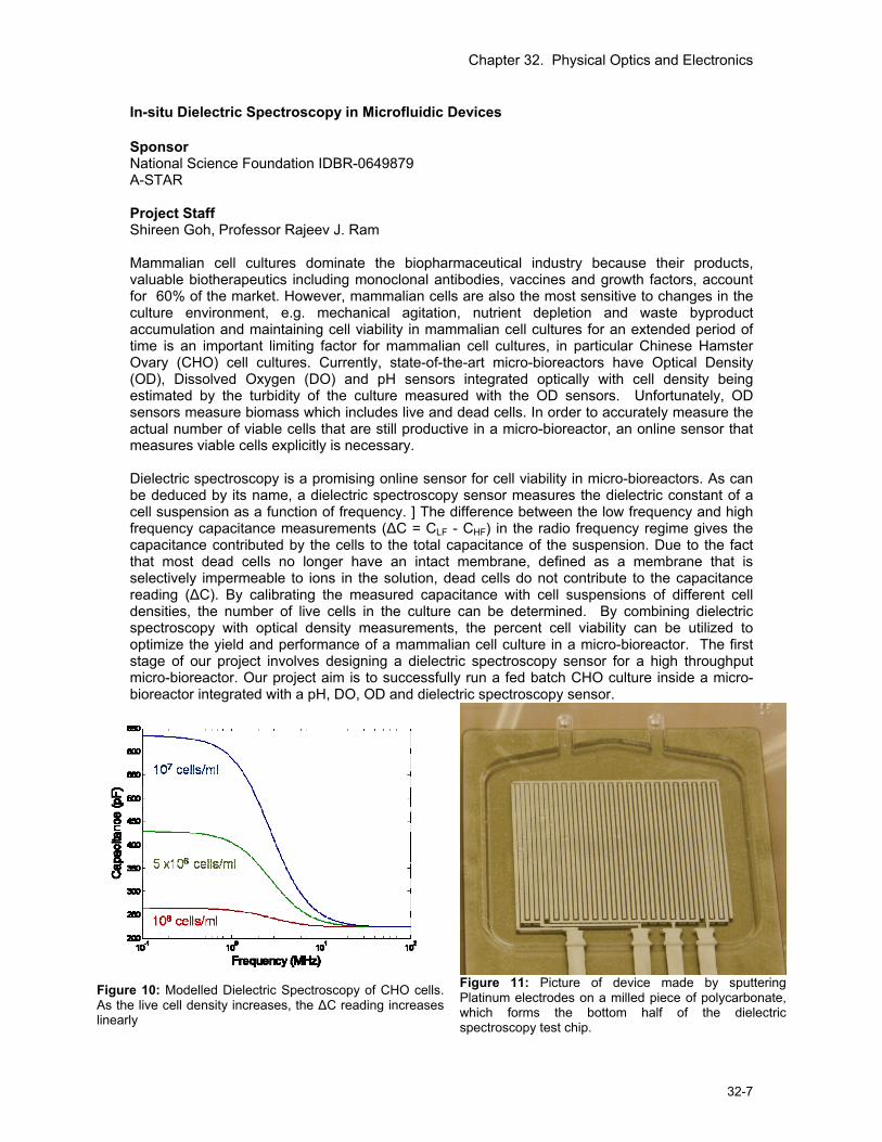
In-situ Dielectric Spectroscopy in Microfluidic Devices Sponsor National Science Foundation IDBR-0649879 A-STAR Project Staff Shireen Goh, Professor Rajeev J. Ram Mammalian cell cultures dominate the biopharmaceutical industry because their products, valuable biotherapeutics including monoclonal antibodies, vaccines and growth factors, account for 60% of the market. However, mammalian cells are also the most sensitive to changes in the culture environment, e.g. mechanical agitation, nutrient depletion and waste byproduct accumulation and maintaining cell viability in mammalian cell cultures for an extended period of time is an important limiting factor for mammalian cell cultures, in particular Chinese Hamster Ovary (CHO) cell cultures. Currently, state-of-the-art micro-bioreactors have Optical Density (OD), Dissolved Oxygen (DO) and pH sensors integrated optically with cell density being estimated by the turbidity of the culture measured with the OD sensors. Unfortunately, OD sensors measure biomass which includes live and dead cells. In order to accurately measure the actual number of viable cells that are still productive in a micro-bioreactor, an online sensor that measures viable cells explicitly is necessary. Dielectric spectroscopy is a promising online sensor for cell viability in micro-bioreactors. As can be deduced by its name, a dielectric spectroscopy sensor measures the dielectric constant of a cell suspension as a function of frequency. ] The difference between the low frequency and high frequency capacitance measurements (∆C = CLF - CHF) in the radio frequency regime gives the capacitance contributed by the cells to the total capacitance of the suspension. Due to the fact that most dead cells no longer have an intact membrane, defined as a membrane that is selectively impermeable to ions in the solution, dead cells do not contribute to the capacitance reading (∆C). By calibrating the measured capacitance with cell suspensions of different cell densities, the number of live cells in the culture can be determined. By combining dielectric spectroscopy with optical density measurements, the percent cell viability can be utilized to optimize the yield and performance of a mammalian cell culture in a micro-bioreactor. The first stage of our project involves designing a dielectric spectroscopy sensor for a high throughput micro-bioreactor. Our project aim is to successfully run a fed batch CHO culture inside a micro-bioreactor integrated with a pH, DO, OD and dielectric spectroscopy sensor.
Figure 10: Modelled Dielectric Spectroscopy of CHO cells. As the live cell density increases, the ∆C reading increases linearly
Figure 11: Picture of device made by sputtering Platinum electrodes on a milled piece of polycarbonate, which forms the bottom half of the dielectric spectroscopy test chip.
Chapter 32. Physical Optics and Electronics
32-8 RLE Progress Report 151
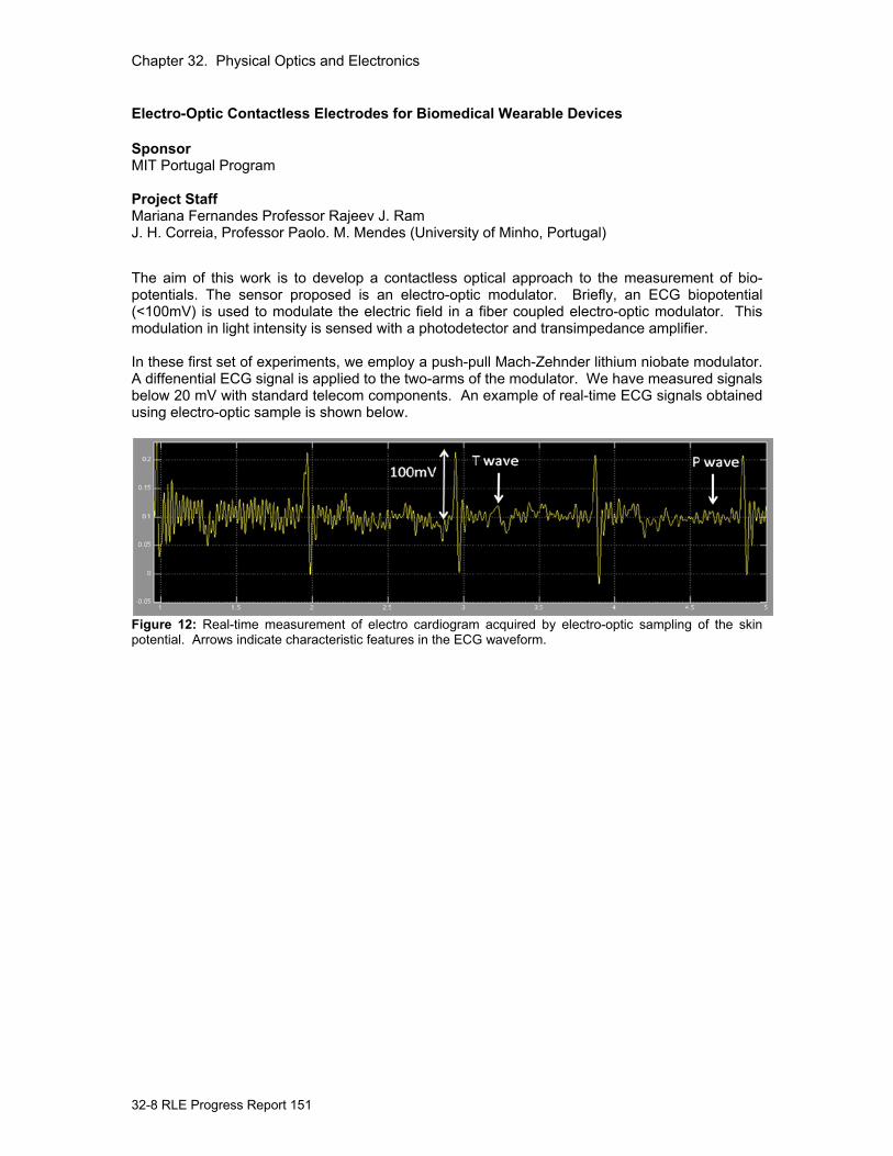
Electro-Optic Contactless Electrodes for Biomedical Wearable Devices Sponsor MIT Portugal Program Project Staff Mariana Fernandes Professor Rajeev J. Ram J. H. Correia, Professor Paolo. M. Mendes (University of Minho, Portugal) The aim of this work is to develop a contactless optical approach to the measurement of bio-potentials. The sensor proposed is an electro-optic modulator. Briefly, an ECG biopotential (<100mV) is used to modulate the electric field in a fiber coupled electro-optic modulator. This modulation in light intensity is sensed with a photodetector and transimpedance amplifier. In these first set of experiments, we employ a push-pull Mach-Zehnder lithium niobate modulator. A diffenential ECG signal is applied to the two-arms of the modulator. We have measured signals below 20 mV with standard telecom components. An example of real-time ECG signals obtained using electro-optic sample is shown below.
Figure 12: Real-time measurement of electro cardiogram acquired by electro-optic sampling of the skin potential. Arrows indicate characteristic features in the ECG waveform.
Chapter 32. Physical Optics and Electronics
32-9
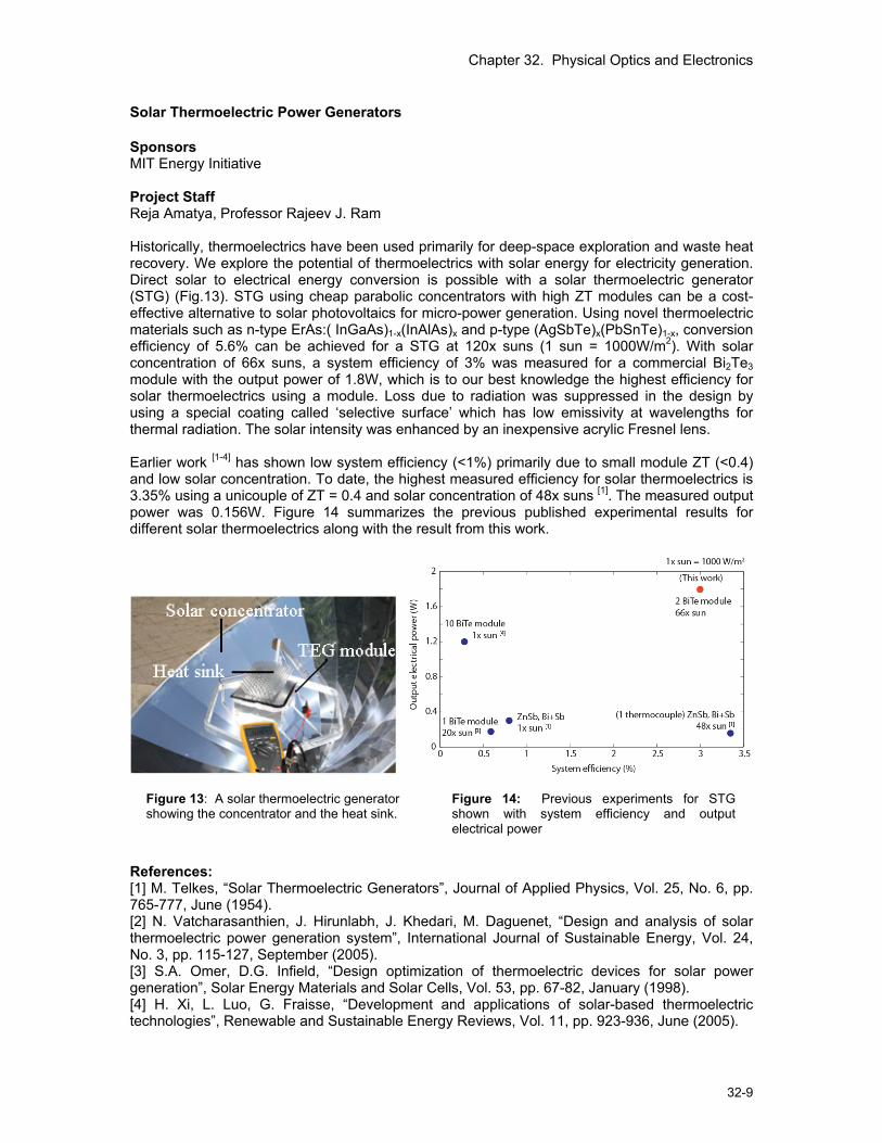
Solar Thermoelectric Power Generators Sponsors MIT Energy Initiative Project Staff Reja Amatya, Professor Rajeev J. Ram Historically, thermoelectrics have been used primarily for deep-space exploration and waste heat recovery. We explore the potential of thermoelectrics with solar energy for electricity generation. Direct solar to electrical energy conversion is possible with a solar thermoelectric generator (STG) (Fig.13). STG using cheap parabolic concentrators with high ZT modules can be a cost-effective alternative to solar photovoltaics for micro-power generation. Using novel thermoelectric materials such as n-type ErAs:( InGaAs)1-x(InAlAs)x and p-type (AgSbTe)x(PbSnTe)1-x, conversion efficiency of 5.6% can be achieved for a STG at 120x suns (1 sun = 1000W/m2). With solar concentration of 66x suns, a system efficiency of 3% was measured for a commercial Bi2Te3 module with the output power of 1.8W, which is to our best knowledge the highest efficiency for solar thermoelectrics using a module. Loss due to radiation was suppressed in the design by using a special coating called ‘selective surface’ which has low emissivity at wavelengths for thermal radiation. The solar intensity was enhanced by an inexpensive acrylic Fresnel lens.
Earlier work [1-4] has shown low system efficiency (<1%) primarily due to small module ZT (<0.4) and low solar concentration. To date, the highest measured efficiency for solar thermoelectrics is 3.35% using a unicouple of ZT = 0.4 and solar concentration of 48x suns [1]. The measured output power was 0.156W. Figure 14 summarizes the previous published experimental results for different solar thermoelectrics along with the result from this work.
References: [1] M. Telkes, “Solar Thermoelectric Generators”, Journal of Applied Physics, Vol. 25, No. 6, pp. 765-777, June (1954). [2] N. Vatcharasanthien, J. Hirunlabh, J. Khedari, M. Daguenet, “Design and analysis of solar thermoelectric power generation system”, International Journal of Sustainable Energy, Vol. 24, No. 3, pp. 115-127, September (2005). [3] S.A. Omer, D.G. Infield, “Design optimization of thermoelectric devices for solar power generation”, Solar Energy Materials and Solar Cells, Vol. 53, pp. 67-82, January (1998). [4] H. Xi, L. Luo, G. Fraisse, “Development and applications of solar-based thermoelectric technologies”, Renewable and Sustainable Energy Reviews, Vol. 11, pp. 923-936, June (2005).
Figure 14: Previous experiments for STG shown with system efficiency and output electrical power
Figure 13: A solar thermoelectric generator showing the concentrator and the heat sink.
Chapter 32. Physical Optics and Electronics
32-10 RLE Progress Report 151
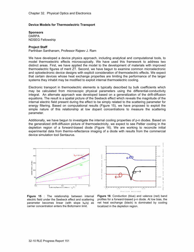
Device Models for Thermoelectric Transport Sponsors DARPA NDSEG Fellowship Project Staff Parthiban Santhanam, Professor Rajeev J. Ram We have developed a device physics approach, including analytical and computational tools, to model thermoelectric effects microscopically. We have used this framework to address two distinct areas. First, we have applied the model to the development of materials with improved thermoelectric figures of merit ZT. Second, we have begun to examine common microelectronic and optoelectronic device designs with explicit consideration of thermoelectric effects. We expect that certain devices whose heat exchange properties are limiting the performance of the larger systems they inhabit may be modified to exploit internal thermoelectric cooling. Electronic transport in thermoelectric elements is typically described by bulk coefficients which may be calculated from microscopic physical parameters using the differential-conductivity integral. An alternate approach was developed based on a generalization of the drift-diffusion equations. The result is a spatial picture of the Seebeck effect which reveals the magnitude of the internal electric field present during the effect to be simply related to the scattering parameter for energy filtering. Based on computational results (Figure 15), we have proposed to exploit the simple nature of this relationship at low dopant concentrations to measure the scattering parameter. Additionally, we have begun to investigate the internal cooling properties of p-n diodes. Based on the generalized drift-diffusion picture of thermoelectricity, we expect to see Peltier cooling in the depletion region of a forward-biased diode (Figure 16). We are working to reconcile initial experimental data from thermo-reflectance imaging of a diode with results from the commercial device simulation tool Sentaurus.
Figure 15 : The relationship between internal electric field under the Seebeck effect and scattering parameter becomes linear (with slope kB/q) as carrier concentration enters the Boltzmann limit.
Figure 16: Conduction (blue) and valence (red) band profiles for a forward-biased p-n diode. At low bias, the net heat exchange (black) is dominated by cooling localized in the depletion region.
Chapter 32. Physical Optics and Electronics
32-11
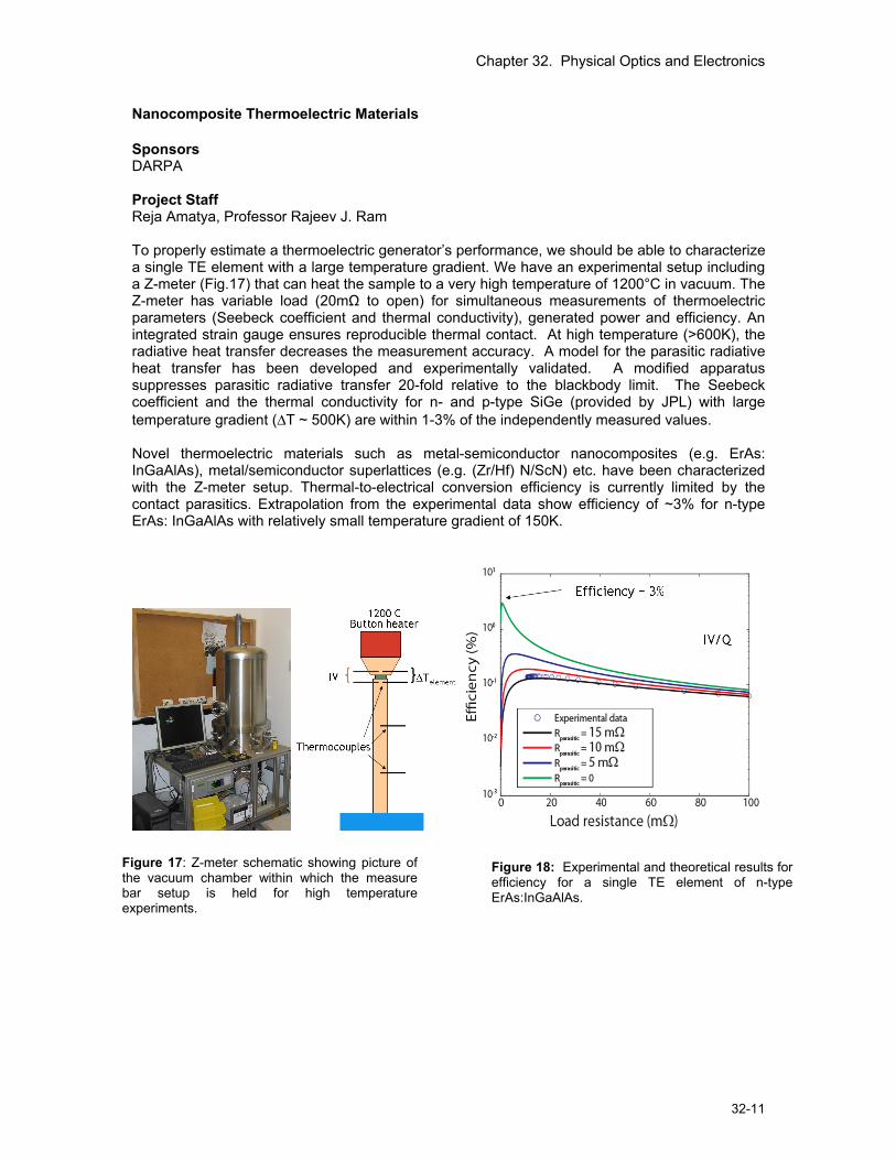
Nanocomposite Thermoelectric Materials Sponsors DARPA Project Staff Reja Amatya, Professor Rajeev J. Ram To properly estimate a thermoelectric generator’s performance, we should be able to characterize a single TE element with a large temperature gradient. We have an experimental setup including a Z-meter (Fig.17) that can heat the sample to a very high temperature of 1200°C in vacuum. The Z-meter has variable load (20mΩ to open) for simultaneous measurements of thermoelectric parameters (Seebeck coefficient and thermal conductivity), generated power and efficiency. An integrated strain gauge ensures reproducible thermal contact. At high temperature (>600K), the radiative heat transfer decreases the measurement accuracy. A model for the parasitic radiative heat transfer has been developed and experimentally validated. A modified apparatus suppresses parasitic radiative transfer 20-fold relative to the blackbody limit. The Seebeck coefficient and the thermal conductivity for n- and p-type SiGe (provided by JPL) with large temperature gradient (ΔT ~ 500K) are within 1-3% of the independently measured values. Novel thermoelectric materials such as metal-semiconductor nanocomposites (e.g. ErAs: InGaAlAs), metal/semiconductor superlattices (e.g. (Zr/Hf) N/ScN) etc. have been characterized with the Z-meter setup. Thermal-to-electrical conversion efficiency is currently limited by the contact parasitics. Extrapolation from the experimental data show efficiency of ~3% for n-type ErAs: InGaAlAs with relatively small temperature gradient of 150K.
Figure 18: Experimental and theoretical results for efficiency for a single TE element of n-type ErAs:InGaAlAs.
Figure 17: Z-meter schematic showing picture of the vacuum chamber within which the measure bar setup is held for high temperature experiments.