Embed Size (px)
Citation preview
Seamless Fail-over for PCIe Switched NetworksWilliam Cheng-Chun Tu
VMware [email protected]
Tzi-cker ChiuehIndustrial Technology Research Institute
ABSTRACTPCI Express (PCIe) was originally designed as a local businterconnect technology for connecting CPUs, GPUs and I/Odevices inside a machine, and has since been enhanced to bea full-blown switched network that features point-to-pointlinks, hop-by-hop flow control, end-to-end retransmission,etc. Recently, researchers have further extended PCIe into anintra-rack interconnect designed to connect multiple hostswithin the same rack. To viably apply PCIe to such use cases ,additional fail-over mechanisms are needed to ensure contin-ued network operation in the presence of control plane anddata plane failures. This paper presents the design, implemen-tation and preliminary evaluation of a fault-tolerant PCIe-based rack area network architecture called Ladon, whichincorporates a fail-over mechanism that takes effective ad-vantage of PCIe architectural features to significantly reducethe service disruption time due to a control plane failureof a PCIe switch. Empirical tests on an operational Ladonprototype show that the proposed mechanism ensures that aPCIe root complex failure has zero impact on the data planeand incurs only a modest disruption time (less than 40 sec)for the control plane services.
1 INTRODUCTIONPeripheral Component Interconnect Express (PCIe) [9] isa computer expansion standard developed by the PCI Spe-cial Interest Group (PCI-SIG) and is designed to serve asa motherboard-level interconnect for on-board devices, apassive backplane interconnect among boards, and an expan-sion interface for connecting amachine with external devicessuch as storage boxes. A PCIe network is a switched networkwith serial point-to-point full duplex lanes, where each at-tached PCIe device is connected to the network through a
Permission to make digital or hard copies of all or part of this work forpersonal or classroom use is granted without fee provided that copiesare not made or distributed for profit or commercial advantage and thatcopies bear this notice and the full citation on the first page. Copyrightsfor components of this work owned by others than the author(s) mustbe honored. Abstracting with credit is permitted. To copy otherwise, orrepublish, to post on servers or to redistribute to lists, requires prior specificpermission and/or a fee. Request permissions from [email protected] ’18, June 4–7, 2018, HAIFA, Israel© 2018 Copyright held by the owner/author(s). Publication rights licensedto Association for Computing Machinery.ACM ISBN 978-1-4503-5849-1/18/06. . . $15.00https://doi.org/10.1145/3211890.3211895
link consisting of one or multiple lanes. The set of devicesconnected to a PCIe network form a PCIe domain, with oneof them serving as the root complex, which is responsible forenumerating and configuring all other devices in the domainand is usually connected to the CPU.Recently, researchers have proposed to replace a top-of-
rack (TOR) Ethernet switch with a PCIe switch, which al-lows all servers in a rack to share all I/O devices in therack [1, 4, 5, 7, 27] and to communicate with one anotherdirectly over PCIe links [10, 16, 28]. To convert PCIe into aviable system interconnect for inter-host communicationswithin a rack, one must first enable multiple hosts to sit onthe same PCIe network and directly communicate with eachother. Although the Multi-Root IO Virtualization (MRIOV)standard [5], published in 2008, was proposed to support mul-tiple root complexes in a single PCIe domain, no commercialimplementations of true MRIOV switches or devices existand there is no sign that there will ever be in the near future.Another approach [27, 28] to establishing direct PCIe con-nectivity among multiple hosts is to leverage a special typeof PCIe device called non-transparent bridge (NTB) [21, 24],which is designed to enable one PCIe domain to directlyaccess resources in another PCIe domain without the in-volvement of the latter’s root complex.
Although PCIe is designed to be lossless at the transac-tion layer with a flow-control and retransmission mecha-nism [9, 19], it does not support any high-level fault toler-ance mechanisms that guarantee a PCIe network’s serviceavailability to the extent which rivals that of traditional sys-tem interconnect technologies such as Ethernet, Infinibandand Fiber Channel. Ladon [27, 28] is a PCIe-based intra-rackinterconnect technology that supports multi-host connectiv-ity using NTB and provides a seamless fail-over mechanismthat effectively addresses the following challenges imposedby the PCIe architecture:
• Because a PCIe domain’s root complex is solely re-sponsible for the configuration of all the devices in thedomain, it represents a single point of failure in thedomain’s control plane.
• Because all devices in a PCIe domain form a hierarchi-cal tree whose root is the root complex, it is inherentlydifficult to provision redundancies and support multi-ple paths between any two devices in the same PCIedomain.
101
SYSTOR ’18, June 4–7, 2018, HAIFA, Israel William Cheng-Chun Tu and Tzi-cker Chiueh
• Since PCIe packet routing is based on target device ad-dresses and PCIe device addresses cannot be modifieddynamically, it is thus difficult to dynamically re-routePCIe packets when link/port failures occur.
This paper addresses the above fault tolerance challengesassociated with a rack-scale PCIe switch-based network thatassumes a SDN-like architecture, i.e., a central controller(root complex) controlling the operations of a number ofpacket-forwarding PCIe switch chips. To handle a root com-plex failure, Ladon enforces a clean separation of controlplane from data plane, and augments the virtual switchmech-anism with a device driver state saving and restore mech-anism so that a slave root complex could seamlessly takeover after the master root complex dies. To enable continuedoperation of a PCIe network in the event of a single PCIelink/switch failure, Ladon partitions a PCIe domain into twophysically disjoint subdomains, connects every host in a rackto two PCIe end points, each of which belongs to a separatesubdomain, assigns two distinct address ranges to each host,and thus makes each host accessible through either one ofthese two address ranges.
2 RELATEDWORKMulti-server interconnection technologies such as FiberChannel, InfiniBand, and Ethernet play a critical role in to-day’s HPC design. Traditionally, out of motherboard-levelapplication of PCIe is used as an I/O expansion switch, whichallows a system to support a larger number of PCIe I/O de-vices where a single motherboard cannot accommodate. Inthe blade server design, multiple servers can connect to onePCIe expansion switch, but requires creating an isolated PCIedomain for each server by re-partitioning a set of PCIe portsto each domain. As a result, each PCIe domain is an inde-pendent network without direct communication through theexpansion switch. Recently, several efforts have been pro-posed to extend the use of PCIe as a high performance andlow power system interconnect solutions [2, 10, 16, 17, 26].
John Byrne et al. [10] shows a PCIe-based network basedon NTB to demonstrate performance gains and 60-124% bet-ter energy efficiency. PEARL [26] demonstrates a power-aware PCIe network and addresses the reliability of the rootcomplex failure by designing their proprietary communica-tion chip. Memory Channel [12, 13] relies on the reflectivememory technology to build a cluster-wide shared memorynetwork. A cluster-wide memory address space is introducedand for each node, a portion of its memory is mapped to theglobal address space. RONNIEE Express Fabric [7] is an inmemory PCIe network for storage systems, which enablesremote memory access between hosts through PCIe and de-livers high performance and scalable file system implemen-tations. As a comparison, Ladon focuses the reliability issues
resulted from extending PCIe into an intra-rack interconnectin a multi-host PCIe system.
Without MR-aware PCIe switch, using a PCIe domain iso-lation and address translation device such as NTB becomes ade facto solution to interconnecting multiple PCIe domains.D. Riley [22] proposes using NTB to redirect CSR for sharedI/O devices. The redirected CSR requests are handled by themanagement host on behalf of the compute host in order tocontrol the I/O devices. Similarly, K. Malwankar. [18] pro-vides multiple proxy devices on a shared PCIe fabric. Theproxy device can be associated with a real I/O device bycopying the configuration space of the real device to theproxy device. As a result, NTB devices are becoming preva-lent as an external devices [21, 23] or embedded in the CPUfeature [24].A server’s particular PCIe bridge connecting to another
server can be pre-configured as either in EP (End Point) modeor RC mode (Root Complex), where the RC-mode server ownthe PCIe switch’s domain and the rest of servers run in EPmode. Several patents have proposed adding failure detec-tion and cable redundancy for multi-host PCIe network. [20]describes solving the master RC failure problem by enablingall the other RCs to periodically detect the liveliness of mas-ter RC, and elect the new RC using system-wise timer. [11]presents a switch fail-over control mechanism by maintain-ing the primary/secondary device table entry (DTE) for theRC andmarks the secondary DTE as passive. Upon a fail-overcondition, updating the secondary DTE in the device table asan active entry and forming a fail-over path to enable trafficrerouting. Ladon is a software-based solution that leveragesthe existing commodity, off-the-shelf components to ensurecontinued network operation in the presence of any singlecontrol plane and data plane failure.
3 PCI EXPRESS ARCHITECTURE3.1 OverviewPCIe is a layered protocol consisting of a physical layer, adata link layer and a transaction layer. The transaction layeris responsible for converting high-level PCIe transactionsissued by the OS or firmware, i.e.,memory, I/O, configurationand message, into PCIe transaction layer packets (TLP). AnX86 machine hosts a PCIe domain, with the root complexresiding in the north bridge, which connects CPU, memoryand the PCIe network, and implements the transaction layerprotocol. Each PCIe device in a PCIe domain is uniquelyidentified by a bus/device/function ID, and is given a setof configuration space registers (CSR), which are partitionedinto a standardized part (such as device/vendor ID, command,base address register or BAR, etc.) and a device-specific part.A PCIe device occupying a PCIe slot functions as one ormultiple physical functions (PF), each acting like a logical
102
Seamless Fail-over for PCIe Switched Networks SYSTOR ’18, June 4–7, 2018, HAIFA, Israel
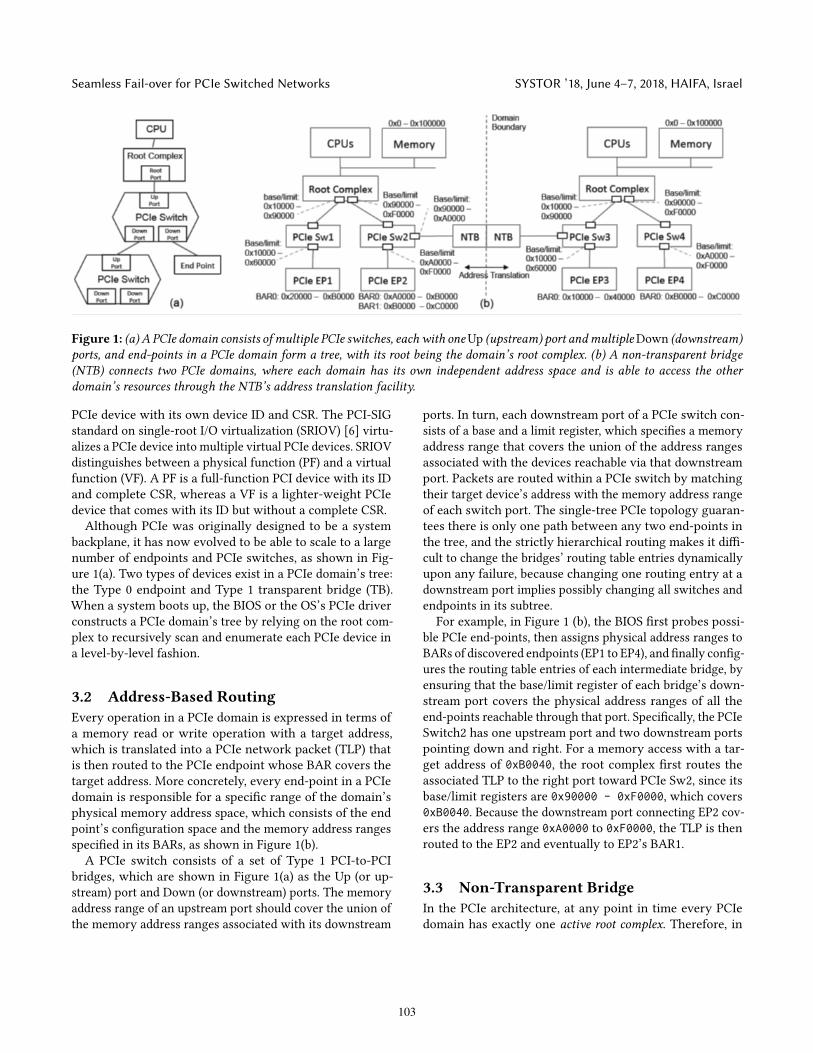
Figure 1: (a) A PCIe domain consists ofmultiple PCIe switches, eachwith oneUp (upstream) port andmultipleDown (downstream)ports, and end-points in a PCIe domain form a tree, with its root being the domain’s root complex. (b) A non-transparent bridge(NTB) connects two PCIe domains, where each domain has its own independent address space and is able to access the otherdomain’s resources through the NTB’s address translation facility.
PCIe device with its own device ID and CSR. The PCI-SIGstandard on single-root I/O virtualization (SRIOV) [6] virtu-alizes a PCIe device into multiple virtual PCIe devices. SRIOVdistinguishes between a physical function (PF) and a virtualfunction (VF). A PF is a full-function PCI device with its IDand complete CSR, whereas a VF is a lighter-weight PCIedevice that comes with its ID but without a complete CSR.Although PCIe was originally designed to be a system
backplane, it has now evolved to be able to scale to a largenumber of endpoints and PCIe switches, as shown in Fig-ure 1(a). Two types of devices exist in a PCIe domain’s tree:the Type 0 endpoint and Type 1 transparent bridge (TB).When a system boots up, the BIOS or the OS’s PCIe driverconstructs a PCIe domain’s tree by relying on the root com-plex to recursively scan and enumerate each PCIe device ina level-by-level fashion.
3.2 Address-Based RoutingEvery operation in a PCIe domain is expressed in terms ofa memory read or write operation with a target address,which is translated into a PCIe network packet (TLP) thatis then routed to the PCIe endpoint whose BAR covers thetarget address. More concretely, every end-point in a PCIedomain is responsible for a specific range of the domain’sphysical memory address space, which consists of the endpoint’s configuration space and the memory address rangesspecified in its BARs, as shown in Figure 1(b).A PCIe switch consists of a set of Type 1 PCI-to-PCI
bridges, which are shown in Figure 1(a) as the Up (or up-stream) port and Down (or downstream) ports. The memoryaddress range of an upstream port should cover the union ofthe memory address ranges associated with its downstream
ports. In turn, each downstream port of a PCIe switch con-sists of a base and a limit register, which specifies a memoryaddress range that covers the union of the address rangesassociated with the devices reachable via that downstreamport. Packets are routed within a PCIe switch by matchingtheir target device’s address with the memory address rangeof each switch port. The single-tree PCIe topology guaran-tees there is only one path between any two end-points inthe tree, and the strictly hierarchical routing makes it diffi-cult to change the bridges’ routing table entries dynamicallyupon any failure, because changing one routing entry at adownstream port implies possibly changing all switches andendpoints in its subtree.For example, in Figure 1 (b), the BIOS first probes possi-
ble PCIe end-points, then assigns physical address ranges toBARs of discovered endpoints (EP1 to EP4), and finally config-ures the routing table entries of each intermediate bridge, byensuring that the base/limit register of each bridge’s down-stream port covers the physical address ranges of all theend-points reachable through that port. Specifically, the PCIeSwitch2 has one upstream port and two downstream portspointing down and right. For a memory access with a tar-get address of 0xB0040, the root complex first routes theassociated TLP to the right port toward PCIe Sw2, since itsbase/limit registers are 0x90000 - 0xF0000, which covers0xB0040. Because the downstream port connecting EP2 cov-ers the address range 0xA0000 to 0xF0000, the TLP is thenrouted to the EP2 and eventually to EP2’s BAR1.
3.3 Non-Transparent BridgeIn the PCIe architecture, at any point in time every PCIedomain has exactly one active root complex. Therefore, in
103
SYSTOR ’18, June 4–7, 2018, HAIFA, Israel William Cheng-Chun Tu and Tzi-cker Chiueh
theory, no two servers each with their own CPUs are al-lowed to co-exist in the same PCIe domain. Non-transparentbridge (NTB), which is a part of the PCI-SIG standard, is de-signed to enable two or more PCIe domains to inter-operatetogether as if they are in a single domain, and thus makes akey building block for Ladon. Conceptually, an NTB is likea layer-3 router in data networking, and isolates the PCIedomains it connects so that the invariant that each PCIedomain has exactly one root complex always holds. A two-port NTB represents two PCIe end-points, each of whichbelongs to one of the two PCIe domains it adjoins. Thesetwo end-points each expose a Type 0 header type in theCSR and thus are discovered and enumerated by the rootcomplex of their respective PCIe domain in the same wayas an ordinary PCIe end-point. However, an NTB providesadditional memory address translation, device ID translationand messaging facilities that allow the two PCIe domainsto work together while keeping them logically isolate fromeach other. More generally, a PCIe switch with X NTB portsand Y TB ports allows the PCIe domain in which the Y TBports participates, called the master domain, to work with Xother PCIe domains, each of which is a slave domain and isreachable via an NTB port. The side of an NTB port that isconnected to a slave domain is the virtual side, whereas theother side is called the link side.
The magic of an NTB lies in its ability to accept a memoryread/write operation initiated from one source PCIe domain,translate its target address, and then deliver and execute itin another PCIe domain. From the initiating domain’s stand-point, the memory read/write operation is logically executedlocally within its domain, although physically it is executedin a remote domain. As mentioned earlier, every PCIe end-point is equipped with a set of BARs that specify the portionsof the physical memory address space of the end-point’s PCIedomain for which it is responsible. That is, all memory readand write operations in a PCIe domain that target at thememory address ranges associated with a PCIe end-point’sBARs are delivered to that end-point. An NTB port associateswith every BAR on the link (virtual) side a memory transla-tion register, which converts a received memory address atthe link (virtual) side into another memory address at thevirtual (link) side. The side of an NTB port providing theBAR is the main side whereas the other side is the supportside. For example in Figure 1(b), two servers each with itsown PCIe domain are connected together using a two-portNTB. Assuming the NTB’s left-hand port is configured totranslate the physical address 0x90000 on its link side to thephysical address 0x0 on its virtual side by writing 0x90000to a link-side BAR and 0x0 to this BAR’s memory transla-tion register. In this case, the link side is the main side andthe virtual side is the support side. A memory read/writeinitiated from the left-hand-side server targeting address
0x90000 will arrive at the BAR of this NTB’s left-hand port,get translated to physical address 0x0 in the right-hand sizePCIe domain, and eventually arrive at the main memory ofthe right-hand side server.Note that address translation in NTB is uni-directional:
only a memory read/write operation that hits a BAR at themain side is translated and relayed to the support side, butnot vice versa. Using the same example, a write operationagainst the address 0x90000 at the link side is translated andrelayed as a write operation against the address 0x0 at thevirtual side, but a write operation against the address 0x0 atthe virtual side is serviced locally and does not automaticallyget translated and relayed to the link side.
3.4 I/O MMUIOMMUprotects the physical memory space of a physical ma-chine or host from unauthorized DMA transactions initiatedby I/O devices by creating another level of address trans-lation: from device virtual address space to physical memoryaddress space. An IOMMU maintains a Translation ControlEntry (TCE) table for device virtual addresses that are used asoperands of DMA operations. Each TCE entry correspondsto a 4KB physical memory page in the host and containsassociated access control bits. When a DMA operation froman I/O device hits the IOMMU, IOMMU searches the TCEusing the source device ID and the operation’s target devicevirtual address, converts the target device virtual addressinto the corresponding physical memory address if there isa matched TCE entry and the DMA operation is compatiblewith the matched TCE entry’s access control bits, and deniesthe DMA operation otherwise.
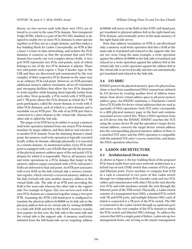
4 LADON ARCHITECTURE4.1 Architectural OverviewAs shown in Figure 2, the key building block of the proposedPCIe-based multi-host rack-area network architecture is ahybrid top-of-rack (TOR) switch that consists of PCIe portsand Ethernet ports. Every machine or compute host (CH)in a rack is connected to two ports of this Ladon switchthrough two independent PCIe extender cards and two PCIecables, and communicates with other CHs in the rack directlyover PCIe and with machines outside the rack through theEthernet ports of the TOR switch. Physically, a Ladon switchconsists of a management host (MH), a standard PCIe switchwith TB and NTB ports, and multiple Ethernet NICs each ofwhich is connected to a TB port of the PCIe switch. The MHis connected to the Ladon switch through an upstream port,and serves as the root complex of the PCIe domain to whichthe PCIe switch and Ethernet NICs belongs. To address theconcern thatMH is a single point of failure, Ladon sets up twomanagement hosts, one serving as the master management
104
Seamless Fail-over for PCIe Switched Networks SYSTOR ’18, June 4–7, 2018, HAIFA, Israel
Figure 2: The key building block of the proposed PCIe-basedintra-rack network architecture is a hybrid top-of-rack switchthat consists of PCIe ports and Ethernet ports. Each computehost (CH) is connected via two distinct NTB ports to the cen-tral PCIe switch, which could be built from multiple PCIeswitch chips. A redundant backup management host (BMH)is passively monitoring the liveliness of the master manage-ment host (MMH). Two Ethernet NICs are attached to the PCIeswitch to support inter-rack communication.
host (MMH) and the other as the backup management host(BMH). The MMH and BMH are connected with a point-to-point Ethernet link, which carries PCIe state synchronizationand heartbeats.Every host connected to a Ladon rack, including the MH
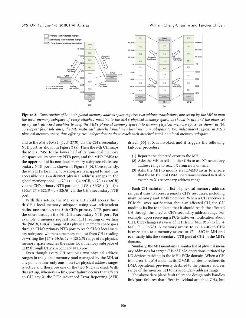
and CHs, has a physical memory space, which in turn com-prises a local memory subspace and non-local memory sub-space. A host’s main memory and MMIO devices are mappedto its local memory subspace. TheMH of a Ladon switchmapsthe local memory subspace of every attached machine toits non-local memory subspace, and in turn every attachedmachine maps the mapped portion of the MH’s physicalmemory space to its non-local memory subspace. The MH’sphysical memory space thus serves as the system’s globalmemory space. For example, assume every machine in therack including the MH has a 32GB local memory subspace.The MH first maps the i-th attached machine’s local memorysubspace to the range [32GB+(i−1)∗32GB, 32GB+i ∗32GB)of its non-local memory space, as shown in Figure 3(a). Theneach attached machine maps the active portion of the MH’sphysical memory space to its non-local memory subspace,which is above 32GB, as shown in Figure 3(b). With thisset-up, an attached machine could access the i-th attachedmachine’s local memory subspace by reading or writing the[64GB + (i − 1) ∗ 32GB, 64GB + i ∗ 32GB) range of its physicalmemory space. In other words, an attached machine couldaccess its local memory resources either directly through
a range in its local memory subspace (below 32GB), or in-directly through a range in its non-local memory subspace(above 64GB). Suppose there are 50 machines attached to aLadon switch, including the MH. Then every attached ma-chine could see a 1600GB worth of physical memory, with32GB local in its own machine (zero hop), 32GB in the MH(one hop) and 1536GB in other attached machines (two hops).Consequently, a Ladon switch ties together the local mem-ory spaces of all the machines attached to it into a globalmemory pool. The physical memory addresses in modern64-bit X86 servers are at least 48 bits long, which is sufficientto support a global memory pool of up to 256TB.
Because every machine connected to a Ladon switch couldpotentially access each physical memory page of every othermachine attached to that switch, data security and safetybecomes a critical issue. More specifically, Ladon must guar-antee that a machine be able to access a remote physicalmemory page in the global memory pool only when it isexplicitly allowed to. Ladon leverages IOMMU [8, 14, 29] toprovide this security guarantee. Every machine attached toa Ladon switch, including the MH, is assigned a unique PCIedevice ID in the MH’s PCIe domain, which remains uniqueafter device ID translation across an NTB port. Therefore,the target address of a PCIe operation from Machine A toMachine C is matched against a different IOMMU mappingtable in Machine C than that used for a PCIe operation fromMachine B to Machine C . To open up a physical memorypage P in Machine C only to Machine B, Ladon places anentry for P in Machine C’s IOMMU mapping table for Ma-chine B, so that memory accesses to P from Machine B couldmatch an entry in this IOMMU mapping table. The abovedesign not only opens up the page P to Machine B, but alsorestricts P ’s accessibility to Machine B only, because no otherIOMMU mapping tables in Machine C contain an entry forPage P . To prevent Machine B from accessing the page P ,Ladon simply removes the entry corresponding to P fromMachine C’s IOMMU mapping table for Machine B.
4.2 Data Plane Fault ToleranceThe MH’s physical memory space is split into two halvescalled PMS1 and PMS2, each of which contains a local mem-ory subspace and a non-local memory subspace. To survivea PCIe link/port failure, Ladon connects each CH to the TORswitch through a primary NTB and a secondary NTB, andmaps each CH’s local memory subspace to two distinct mem-ory address ranges in MH’s physical memory space, onein PMS1 and the other in PMS2. The example in Figure 3assumes that each CH needs a 32GB local memory subspacefor its main memory and memory mapped I/O (MMIO) de-vices. Ladon maps the i-th CH’s local memory subspace tothe MH’s PMS1 ([0, 1TB)) via the CH’s primary NTB port
105
SYSTOR ’18, June 4–7, 2018, HAIFA, Israel William Cheng-Chun Tu and Tzi-cker Chiueh
Figure 3: Construction of Ladon’s global memory address space requires two address translations; one set up by the MH to mapthe local memory subspace of every attached machine to the MH’s physical memory space, as shown in (a), and the other setup by each attached machine to map the MH’s physical memory space into its own physical memory space, as shown in (b).To support fault tolerance, the MH maps each attached machine’s local memory subspace to two independent regions in MH’sphysical memory space, thus offering two independent paths to reach each attached machine’s local memory subspace.
and to the MH’s PMS2 ([1TB, 2TB)) via the CH’s secondaryNTB port, as shown in Figure 3 (a). Then the i-th CH mapsthe MH’s PMS1 to the lower half of its non-local memorysubspace via its primary NTB port, and the MH’s PMS2 tothe upper half of its non-local memory subspace via its sec-ondary NTB port, as shown in Figure 3 (b). Consequently,the i-th CH’s local memory subspace is mapped to and thusaccessible via two distinct physical address ranges in theglobal memory pool, [32GB+ (i −1) ∗32GB, 32GB+ i ∗32GB)via the CH’s primary NTB port, and [1TB + 32GB + (i − 1) ∗32GB, 1T + 32GB + i ∗ 32GB) via the CH’s secondary NTBport.With this set-up, the MH or a CH could access the i-
th CH’s local memory subspace using two independentpaths, one through the i-th CH’s primary NTB port, andthe other through the i-th CH’s secondary NTB port. Forexample, a memory request from CH1 reading or writingthe [96GB, 128GB) range of its physical memory space goesthrough CH2’s primary NTB port to reach CH2’s local mem-ory subspace, whereas a memory request from CH1 readingor writing the [1T + 96GB, 1T + 128GB) range of its physicalmemory space reaches the same local memory subspace ofCH2 through CH2’s secondary NTB port.Even though every CH occupies two physical address
ranges in the global memory pool managed by the MH, atany point in time, only one of the two physical address rangesis active and therefore one of the two NTBs is used. Withthis set-up, whenever a link/port failure occurs that affectsan CH, say X, the PCIe Advanced Error Reporting (AER)
driver [30] at X is invoked, and it triggers the followingfail-over procedure:
(1) Reports the detected error to the MH,(2) Asks the MH to tell all other CHs to use X’s secondary
address range to reach X from now on, and(3) Asks the MH to modify its IOMMU so as to ensure
that the MH’s local DMA operations destined to X alsoswitch to X’s secondary address range.
Each CH maintains a list of physical memory addressranges it uses to access a remote CH’s resources, includingmain memory and MMIO devices. When a CH receives aPCIe fail-over notification about an affected CH, the CHmodifies its list to indicate that it should reach the affectedCH through the affected CH’s secondary address range. Forexample, upon receiving a PCIe fail-over notification aboutCH1, CH2 changes its view of CH1 from [64G, 96G) to [1T +64G, 1T + 96GB). A memory access to 1T + 64G in CH2is translated to a memory access to 1T + 32G in MH andeventually hits the secondary NTB port of CH1 in the MH’sdomain.
Similarly, the MHmaintains a similar list of physical mem-ory addresses for target CHs of DMA operations initiated byI/O devices residing in the MH’s PCIe domain. When a CHis in error, the MH modifies its IOMMU entries to redirect itsDMA operations previously destined to the primary addressrange of the in-error CH to its secondary address range.
The above data plane fault tolerance design only handleslink/port failures that affect individual attached CHs, but
106
Seamless Fail-over for PCIe Switched Networks SYSTOR ’18, June 4–7, 2018, HAIFA, Israel
cannot deal with entire PCIe switch failures or inter-switchlink failures, which are left for future work.
4.3 Control Plane Fault Tolerance
4.3.1 Control Migration between Management Hosts
The management host (MH) of a Ladon switch is respon-sible for the mapping of the attached CHs’ physical memoryspaces into its physical memory space, and for exposing itsphysical memory space, including the address range associ-ated with its PCIe devices, e.g. NICs, to the attached CHs in asecure way. After address allocation of each PCIe device, theMH configures the routing table of each PCIe bridge in thehierarchical routing tree, so that PCIe packets could be for-warded accordingly. Once the MH completes this set-up, itsrole becomes visible only when there is a change in its PCIedomain, i.e., addition or deletion of PCIe end-points. Mostnotably, the MH is not involved at all in the peer-to-peerdata transfers among the PCIe end-points. In fact, when theMH dies, as long as the routing states in P2P bridges remain,the PCIe end-points could continue to exchange data withone another without any pauses. So when the MH fails, itis neither necessary nor desirable to recover from such afailure immediately, especially because the current recoveryprocedure for a MH failure requires a system-wide restartof all PCIe end points, which in turn may trigger at leasta device driver reset and possibly a system reboot on theattached CHs. This subsection describes a seamless controlplane fail-over mechanism that enables the data plane tocontinue operating without any disruption when the MHfails and recovers.To achieve seamless fail-over across a MH failure, Ladon
sets up two management hosts, one serving as the mastermanagement host (MMH) and the other as the backup man-agement host (BMH). The MMH and BMH are connectedwith a point-to-point Ethernet link, which carries PCIe statesynchronization and heartbeats. In addition, the MMH syn-chronously replicates modifications to the following statesto the BMH over the dedicated Ethernet link:
• Results of initial PCIe device scanning and enumera-tion, including assignments of physical address ranges,interrupt numbers, etc.,
• Contents of the BARs, translation registers, device IDtranslation tables, IOMMUs of the NTB ports,
• Allocation of virtual functions (VFs) of PCIe devicessupporting single-root IO Virtualization (SRIOV) toattached machines, and
• Internal states of the PCIe device drivers in its domain.Modern PCIe switch chips, including the PCIe switch used
in this project, support a capability to partition a physical
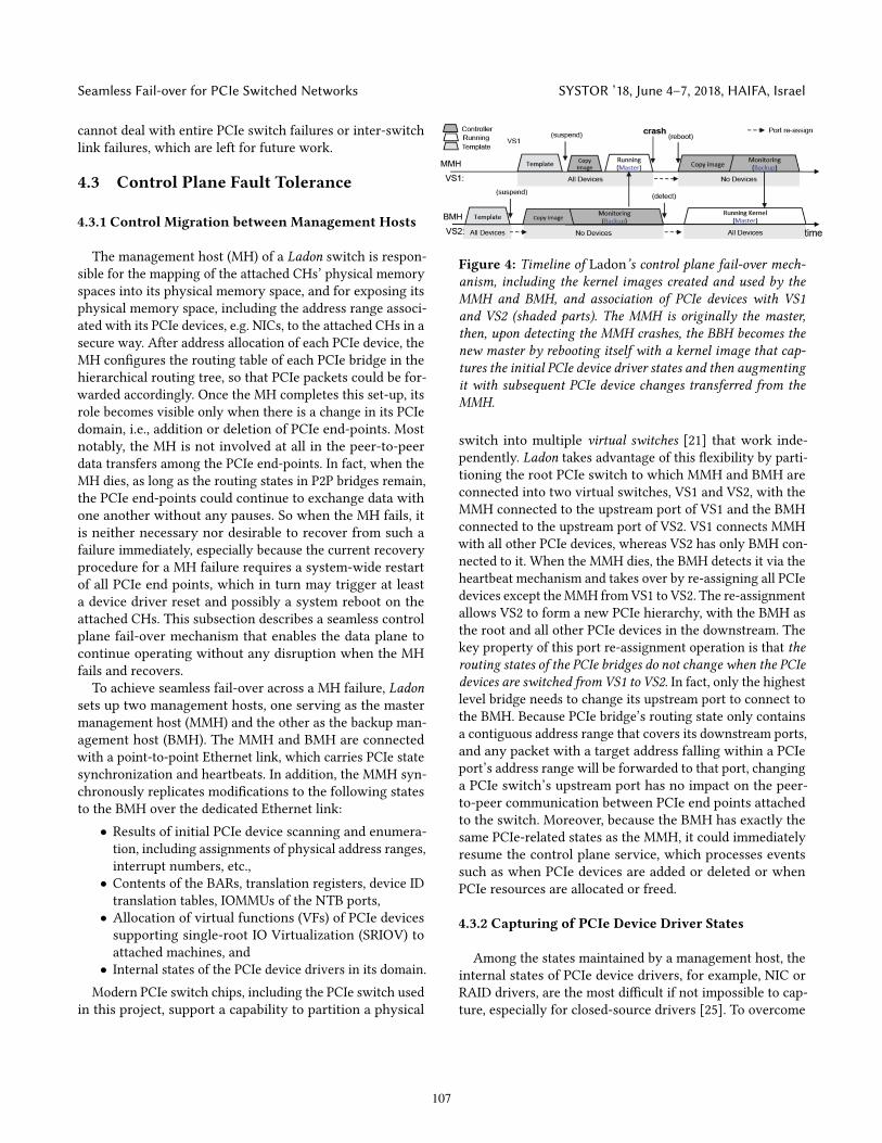
Figure 4: Timeline of Ladon’s control plane fail-over mech-anism, including the kernel images created and used by theMMH and BMH, and association of PCIe devices with VS1and VS2 (shaded parts). The MMH is originally the master,then, upon detecting the MMH crashes, the BBH becomes thenew master by rebooting itself with a kernel image that cap-tures the initial PCIe device driver states and then augmentingit with subsequent PCIe device changes transferred from theMMH.
switch into multiple virtual switches [21] that work inde-pendently. Ladon takes advantage of this flexibility by parti-tioning the root PCIe switch to which MMH and BMH areconnected into two virtual switches, VS1 and VS2, with theMMH connected to the upstream port of VS1 and the BMHconnected to the upstream port of VS2. VS1 connects MMHwith all other PCIe devices, whereas VS2 has only BMH con-nected to it. When the MMH dies, the BMH detects it via theheartbeat mechanism and takes over by re-assigning all PCIedevices except theMMH fromVS1 to VS2. The re-assignmentallows VS2 to form a new PCIe hierarchy, with the BMH asthe root and all other PCIe devices in the downstream. Thekey property of this port re-assignment operation is that therouting states of the PCIe bridges do not change when the PCIedevices are switched from VS1 to VS2. In fact, only the highestlevel bridge needs to change its upstream port to connect tothe BMH. Because PCIe bridge’s routing state only containsa contiguous address range that covers its downstream ports,and any packet with a target address falling within a PCIeport’s address range will be forwarded to that port, changinga PCIe switch’s upstream port has no impact on the peer-to-peer communication between PCIe end points attachedto the switch. Moreover, because the BMH has exactly thesame PCIe-related states as the MMH, it could immediatelyresume the control plane service, which processes eventssuch as when PCIe devices are added or deleted or whenPCIe resources are allocated or freed.
4.3.2 Capturing of PCIe Device Driver States
Among the states maintained by a management host, theinternal states of PCIe device drivers, for example, NIC orRAID drivers, are the most difficult if not impossible to cap-ture, especially for closed-source drivers [25]. To overcome
107
SYSTOR ’18, June 4–7, 2018, HAIFA, Israel William Cheng-Chun Tu and Tzi-cker Chiueh
this implementation challenge, Ladon leverages Linux’s sus-pend/resume [3, 15] facility, in which when the suspendoperation is invoked, the entire system state including thedrivers’ states, are snapshotted and saved to the disk.
Specifically, both the MMH and BMH have three disk par-titions that hold three different kernel images: the controllerkernel image, the template kernel image, and the running ker-nel image. The controller kernel is used to boot up a man-agement host so as to manage the other two kernel images.The template kernel is used to hold a golden kernel imageto be reused after a failure, and is created from a suspendoperation of the system after all PCIe device drivers are ini-tialized. The running kernel is the kernel MMH and BMHruns to perform management host functions.
As shown in Figure 4, initially all PCIe devices except theMMH are connected to VS2, and the BMH boots up from thecontroller kernel image until all of its PCIe device driversare initialized. Then the BMH suspends itself to form thetemplate kernel image, reboots itself from the controller im-age, and then copies the template image to form the runningimage. Finally the BMH is again rebooted from the controllerimage, and, from this point on, monitors the health of MMHusing heartbeat messages.
Next, all PCIe devices except the BMH are re-assigned toVS1, and the MMH boots up from the controller image andcontinues to run until all of its PCIe device drivers are ini-tialized. Then the MMH suspends itself to form the templateimage, reboots itself again from the controller image, andthen copies the template image to form the running image.Finally the MMH reboots itself once more, this time fromthe running image, and gets the whole system going.When the BMH detects that the MMH encounters an ir-
recoverable error, the BMH instructs all other members ofVS1 except the MMH to join VS2, and reboots itself usingthe running image. Because the BMH’s running image con-tains all the necessary PCIe device driver states, the BMHis able to manage the PCIe devices and NTBs in VS2’s PCIedomainwithout resetting them. Note that the BMHmust reas-sign members of VS1 to VS2 before rebooting itself, becauseotherwise the reboot may fail as the device drivers in therunning kernel image could not find their correspondingdevices. The control plane’s service is disrupted during thetime only when the BMH is rebooted.The suspend/resume-based approach is simple to imple-
ment because it does not require understanding of or modifi-cations to PCIe device drivers. However, it is limited in that itcannot accommodate any run-time changes to PCIe devicesor PCIe resource allocation after the initial snapshots weretaken. To account for these changes, the MMH must log andtransfer them via the dedicated Ethernet link to BMH at runtime, and the BMH replays them after rebooting itself usingthe running kernel image during the take-over process.
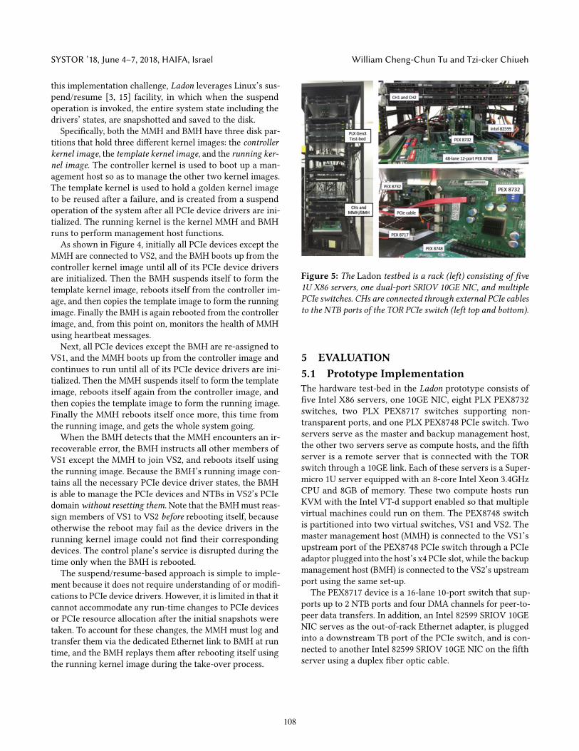
Figure 5: The Ladon testbed is a rack (left) consisting of five1U X86 servers, one dual-port SRIOV 10GE NIC, and multiplePCIe switches. CHs are connected through external PCIe cablesto the NTB ports of the TOR PCIe switch (left top and bottom).
5 EVALUATION5.1 Prototype ImplementationThe hardware test-bed in the Ladon prototype consists offive Intel X86 servers, one 10GE NIC, eight PLX PEX8732switches, two PLX PEX8717 switches supporting non-transparent ports, and one PLX PEX8748 PCIe switch. Twoservers serve as the master and backup management host,the other two servers serve as compute hosts, and the fifthserver is a remote server that is connected with the TORswitch through a 10GE link. Each of these servers is a Super-micro 1U server equipped with an 8-core Intel Xeon 3.4GHzCPU and 8GB of memory. These two compute hosts runKVM with the Intel VT-d support enabled so that multiplevirtual machines could run on them. The PEX8748 switchis partitioned into two virtual switches, VS1 and VS2. Themaster management host (MMH) is connected to the VS1’supstream port of the PEX8748 PCIe switch through a PCIeadaptor plugged into the host’s x4 PCIe slot, while the backupmanagement host (BMH) is connected to the VS2’s upstreamport using the same set-up.The PEX8717 device is a 16-lane 10-port switch that sup-
ports up to 2 NTB ports and four DMA channels for peer-to-peer data transfers. In addition, an Intel 82599 SRIOV 10GENIC serves as the out-of-rack Ethernet adapter, is pluggedinto a downstream TB port of the PCIe switch, and is con-nected to another Intel 82599 SRIOV 10GE NIC on the fifthserver using a duplex fiber optic cable.
108
Seamless Fail-over for PCIe Switched Networks SYSTOR ’18, June 4–7, 2018, HAIFA, Israel
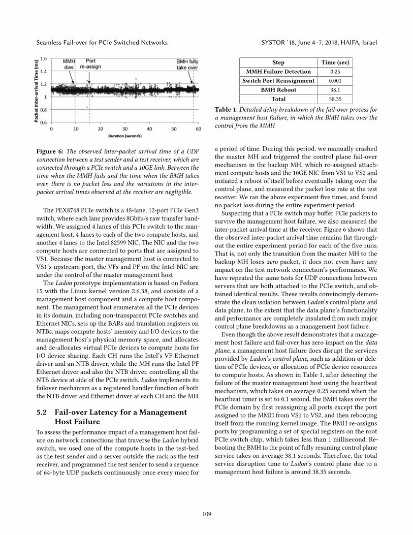
Figure 6: The observed inter-packet arrival time of a UDPconnection between a test sender and a test receiver, which areconnected through a PCIe switch and a 10GE link. Between thetime when the MMH fails and the time when the BMH takesover, there is no packet loss and the variations in the inter-packet arrival times observed at the receiver are negligible.
The PEX8748 PCIe switch is a 48-lane, 12-port PCIe Gen3switch, where each lane provides 8Gbits/s raw transfer band-width. We assigned 4 lanes of this PCIe switch to the man-agement host, 4 lanes to each of the two compute hosts, andanother 4 lanes to the Intel 82599 NIC. The NIC and the twocompute hosts are connected to ports that are assigned toVS1. Because the master management host is connected toVS1’s upstream port, the VFs and PF on the Intel NIC areunder the control of the master management hostThe Ladon prototype implementation is based on Fedora
15 with the Linux kernel version 2.6.38, and consists of amanagement host component and a compute host compo-nent. The management host enumerates all the PCIe devicesin its domain, including non-transparent PCIe switches andEthernet NICs, sets up the BARs and translation registers onNTBs, maps compute hosts’ memory and I/O devices to themanagement host’s physical memory space, and allocatesand de-allocates virtual PCIe devices to compute hosts forI/O device sharing. Each CH runs the Intel’s VF Ethernetdriver and an NTB driver, while the MH runs the Intel PFEthernet driver and also the NTB driver, controlling all theNTB device at side of the PCIe switch. Ladon implements itsfailover mechanism as a registered handler function of boththe NTB driver and Ethernet driver at each CH and the MH.
5.2 Fail-over Latency for a ManagementHost Failure
To assess the performance impact of a management host fail-ure on network connections that traverse the Ladon hybridswitch, we used one of the compute hosts in the test-bedas the test sender and a server outside the rack as the testreceiver, and programmed the test sender to send a sequenceof 64-byte UDP packets continuously once every msec for
Step Time (sec)MMH Failure Detection 0.25
Switch Port Reassignment 0.001BMH Reboot 38.1
Total 38.35
Table 1: Detailed delay breakdown of the fail-over process fora management host failure, in which the BMH takes over thecontrol from the MMH
a period of time. During this period, we manually crashedthe master MH and triggered the control plane fail-overmechanism in the backup MH, which re-assigned attach-ment compute hosts and the 10GE NIC from VS1 to VS2 andinitiated a reboot of itself before eventually taking over thecontrol plane, and measured the packet loss rate at the testreceiver. We ran the above experiment five times, and foundno packet loss during the entire experiment period.
Suspecting that a PCIe switch may buffer PCIe packets tosurvive the management host failure, we also measured theinter-packet arrival time at the receiver. Figure 6 shows thatthe observed inter-packet arrival time remains flat through-out the entire experiment period for each of the five runs.That is, not only the transition from the master MH to thebackup MH loses zero packet, it does not even have anyimpact on the test network connection’s performance. Wehave repeated the same tests for UDP connections betweenservers that are both attached to the PCIe switch, and ob-tained identical results. These results convincingly demon-strate the clean isolation between Ladon’s control plane anddata plane, to the extent that the data plane’s functionalityand performance are completely insulated from such majorcontrol plane breakdowns as a management host failure.
Even though the above result demonstrates that a manage-ment host failure and fail-over has zero impact on the dataplane, a management host failure does disrupt the servicesprovided by Ladon’s control plane, such as addition or dele-tion of PCIe devices, or allocation of PCIe device resourcesto compute hosts. As shown in Table 1, after detecting thefailure of the master management host using the heartbeatmechanism, which takes on average 0.25 second when theheartbeat timer is set to 0.1 second, the BMH takes over thePCIe domain by first reassigning all ports except the portassigned to the MMH from VS1 to VS2, and then rebootingitself from the running kernel image. The BMH re-assignsports by programming a set of special registers on the rootPCIe switch chip, which takes less than 1 millisecond. Re-booting the BMH to the point of fully resuming control planeservice takes on average 38.1 seconds. Therefore, the totalservice disruption time to Ladon’s control plane due to amanagement host failure is around 38.35 seconds.
109
SYSTOR ’18, June 4–7, 2018, HAIFA, Israel William Cheng-Chun Tu and Tzi-cker Chiueh
Step Time (µsec)Link Failure Detection 2.4Failure Determination 8.5
Route Change Notification and Processing 76Total 86.9
Table 2: Detailed delay breakdown of the fail-over process fora link/port failure associated with a compute host
In contrast, without Ladon’s control plane fail-overscheme, after detecting the MMH fails, the BMH must firstinitiate a system-wide shut-down and restart to all CHs, andthen reboots itself to resume the services on the data andcontrol plane. The entire process takes about 85 seconds.During this period, the data plane service is unavailable andno packets can travel on the PCIe network.
5.3 Fail-over Latency for a Link FailureThe current Ladon prototype only handles failures oflinks/ports associated with an CH. To efficiently handle PCIelink/switch failures, Ladon detects occurrences of failuresby leveraging PCIe’s advanced error reporting (AER) [30]capability, which allows a PCIe component to send an errorreporting message to the root complex. Such error signal-ing can occur because of a failure of a PCIe link or of atransaction initiated on a PCIe link. Table 2 shows the delaybreakdown of the fail-over process of such a failure, whichis broken down into the following three components.
Failure Detection: This is the time between when a PCIedevice detects an uncorrectable fatal error and sends an errormessage to the root complex and triggers an interrupt, andwhen the PCIe AER driver responds to the interrupt. In ourprototype, the link failure detection time is around 2.4 µsec.
Failure Determination: When a CH’s AER driver receivesan AER interrupt, it notifies the MH, which makes a finalverdict on whether it is indeed a data plane failure that de-serves a fail-over action. In the current Ladon prototype, aCH’s AER driver notifies the MH by writing to a pre-defined4-byte memory location, which a thread on the MH pollsconstantly and, upon detecting a change, reads it and imme-diately writes a response into a pre-defined 4-byte location inthe CH. The round-trip delay as measured by a CH’s AER dri-ver is 17 µsec, which suggests that the one-way notificationdelay is 8.5 µsec.
Route Change Notification and Processing: After determin-ing a fail-over action is justified, the MH notifies all the CHsabout the route change one by one. As a result, the totalnotification latency from the MH to all CHs becomes thenumber of CHs times 8.5 µsec. As mentioned in Section 4.2,each CH maintains a list of physical memory addresses ituses to access a remote CH’s resources, and, upon receiving a
fail-over notification about an in-error CH, modifies this listto ensure that all subsequent accesses to the in-error CH useits secondary address range. Modification to this list takesless than 1 µsec. Because the current prototype could holdup to 8 CHs, the total notification delay is around 8*(1+8.5)= 76 µsec.In summary, the total fail-over latency for a link failure
in the current prototype (up to 8 CHs) is about 86.9 µsec,the bulk of which is attributed to route change notification.This route change notification delay could be significantlyreduced if Ladon exploits the multicast capability of modernPCIe switches, where a memory write operation with a mul-ticast target address is sent to all PCIe end points that belongto the corresponding multicast group.
6 CONCLUSIONBecause PCI Express’s transceiver is designed for short dis-tance (less than 10 meters), it is simpler, cheaper, and morepower-efficient, and makes a more cost- and power-efficientsystem area network for intra-rack inter-machine communi-cations than comparable technologies such as 10Gbps Eth-ernet or Infiniband. Its memory-based addressing model isespecially compelling because it opens up the possibility foronemachine to directly read or write anymemory location ofanother machine without involving the latter’s CPU. Ladonexploits this direct remote memory access capability to setup its fail-over mechanisms that ensure continued networkoperation in the presence of a control/data plane failure. Thispaper presents the design, implementation and evaluation ofa fault-tolerant PCIe-based rack area network architecturethat takes effective advantage of PCIe architectural featuresto significantly reduce the service disruption time due toa failure of a PCIe root complex and a PCIe link/port. Thespecific research contributions of this work thus include:
• A fault-tolerant PCIe-based rack-area interconnect ar-chitecture that connects together a set of computehosts and PCIe devices, and allows each compute host’sresources to be mapped into two distinct memory ad-dress ranges in a rack-wide global memory space andthus be accessible via two independent paths, and
• Design of a seamless data plane fail-over mechanismthat detects a PCIe link/port failure and the affectedcompute host, notifies the management host, and getsall other compute hosts to communicate with the af-fected compute host using its secondary address rangefrom this point on, and
• Design, implementation and evaluation of a seamlesscontrol plane fail-over mechanism that successfullyprevents a control plane failure from disrupting thedata plane and incurs only a modest service disruptiontime on the control plane service.
110
Seamless Fail-over for PCIe Switched Networks SYSTOR ’18, June 4–7, 2018, HAIFA, Israel
REFERENCES[1] [n. d.]. I/O ConsolidationWhite Paper, NextIO, Inc. http://www.nextio.
com/resources/files/wp-nextio-consolidation.pdf. ([n. d.]). accessedJune 4, 2012.
[2] [n. d.]. PCI Express System Interconnect Software Architecture forx86-based Systems. http://www.idt.com. ([n. d.]). K. Kong, September2008.
[3] [n. d.]. TuxOnIce. Revolutionize the way you start your computer.http://tuxonice.net/. ([n. d.]).
[4] [n. d.]. Xsigo Systems, Inc. http://en.wikipedia.org/wiki/XsigoSystems.([n. d.]). accessed in July 2017.
[5] 2008. Multi-Root I/O Virtualization and Sharing 1.0 Specification,PCI-SIG Standard. (2008).
[6] 2008. Single-Root I/O Virtualization and Sharing Specification, Revi-sion 1.0, PCI-SIG Standard. (2008).
[7] A3Cube Inc. [n. d.]. RONNIEE Express Fabric - The In Memory Net-work . http://www.a3cube-inc.com/ronniee-express.html. ([n. d.]).
[8] M. Ben-Yehuda, J. Mason, J. Xenidis, O. Krieger, L. Van Doorn, J. Naka-jima, A. Mallick, and E. Wahlig. 2006. Utilizing IOMMUs for virtualiza-tion in Linux and Xen. In OLS06: The 2006 Ottawa Linux Symposium.71–86.
[9] R. Budruk, D. Anderson, and T. Shanley. 2004. PCI Express SystemArchitecture. Addison-Wesley Professional.
[10] J. Byrne, J. Chang, K.T. Lim, L. Ramirez, and P. Ranganathan. 2011.Power-Efficient Networking for Balanced System Designs: Early Expe-riences with PCIe. In Proceedings of the 4th Workshop on Power-AwareComputing and Systems. ACM, 3.
[11] G. K. Bayer and D. F. Craddock and T. A. Gregg and M. Jung and A.Kohler and E. G. Nass and O. G. Schlag and P. K. Szwed . [n. d.]. Switchfailover control in a multiprocessor computer system. ([n. d.]). Mar.18 2014, US Patent 8,677,180.
[12] R. Gillett. 1996. Memory channel network for pci. IEEE Micro, vol.16,no.1 (1996), 12–18.
[13] R. Gillett and R. Kaufmann. 1997. Using the memory channel channelnetwork. IEEE Micro, vol.17, no.1 (1997), 19–25.
[14] R. Hiremane. 2007. Intel Virtualization Technology for Directed I/O(Intel VT-d). Technology@ Intel Magazine 4, 10 (2007).
[15] Hui-Hao Chiang and Maohua Lu and Tzi-cker Chiueh. 2011. PhysicalMachine State Migration. In Proceedings of IEEE 17th InternationalConference on Parallel and Distributed Systems (ICPADS). 25–32.
[16] V. Krishnan. 2007. Towards an Integrated IO and Clustering SolutionUsing PCI Express. In Proceedings of 2007 IEEE International ConferenceonCluster Computing. IEEE, 259–266.
[17] V. Krishnan. 2008. Evaluation of an integrated pci express io expansionand clustering fabric. In Proceedings of 16th IEEE Symposium on HighPerformance Interconnects (HOTI âĂŹ08). 93–100.
[18] K. Malwankar, D. Talayco, and A. Ekici. 2009. PCI-Express FunctionProxy. (Oct. 1 2009). WO Patent WO/2009/120,798.
[19] D. Mayhew and V. Krishnan. 2003. PCI Express and Advanced Switch-ing: Evolutionary Path to Building Next Generation Interconnects.In Proceedings of 11th Symposium on High Performance Interconnects.IEEE, 21–29.
[20] R. L. Billau and J. D. Folkerts and R. L. Franke and J. S. Harveland andB. G. Holthaus. [n. d.]. Autonomic pci express hardware detection andfailover mechanism. ([n. d.]). Aug. 29 2007, US Patent App. 11/846,783.
[21] J. Regula. 2004. Using Non-Transparent Bridging in PCI Express Sys-tems. PLX Technology, Inc (2004).
[22] D.D. Riley. 2012. System and Method for Multi-Host Sharing of aSingle-Host Device. (May 8 2012). US Patent 8,176,204.
[23] STMicroelectronics. [n. d.]. iATU Operations, SPEAr1340architecture and functionality reference manual. http:
//www.st.com/st-web-ui/static/active/en/resource/technical/document/referencemanual/DM00024168.pdf. ([n. d.]).
[24] Mark J. Sullivan. 2010. Intel Xeon Processor C5500/C3500 Series Non-Transparent Bridge. Technology@ Intel Magazine (2010).
[25] M. M. Swift, M. Annamalai, B. N. Bershad, and H. M. Levy. 2006.Recovering device drivers. ACM Transactions on Computer Systems(TOCS), vol. 24, no.4 (2006), 333âĂŞ–360.
[26] T. Hanawa and T. Boku and S. Miura and M. Sato and K. Arimoto. 2010.Pearl: Poweraware, dependable, and high-performance communica-tion link using pci express. In Proceedings of IEEE/ACM InternationalConference on Green Computing and Communications (GreenCom) andon Cyber, Physical and Social Computing (CPSCom). IEEE, 284–291.
[27] William Tu and Mark Lee and Tzi-cker Chiueh. 2013. Secure i/o devicesharing among virtual machines on multiple hosts. In Proceedings ofACM International Symposium on Computer Architecture. ACM, 108–119.
[28] WilliamTu and Tzi-cker Chiueh andMark Lee. 2014. Marlin: amemory-based rack area network. In Proceedings of the tenth ACM/IEEE sym-posium on Architectures for Networking and Communications Systems.ACM, 125–136.
[29] P. Willmann, S. Rixner, and A.L. Cox. 2008. Protection Strategies forDirect Access to Virtualized I/O Devices. In USENIX Annual TechnicalConference. 15–28.
[30] Y. Zhang and T. L. Nguyen. 2007. Enable pci express advanced errorreporting in the kernel. In 2007 Ottawa Linux Symposium. 297–304.
111