Embed Size (px)
Citation preview
R
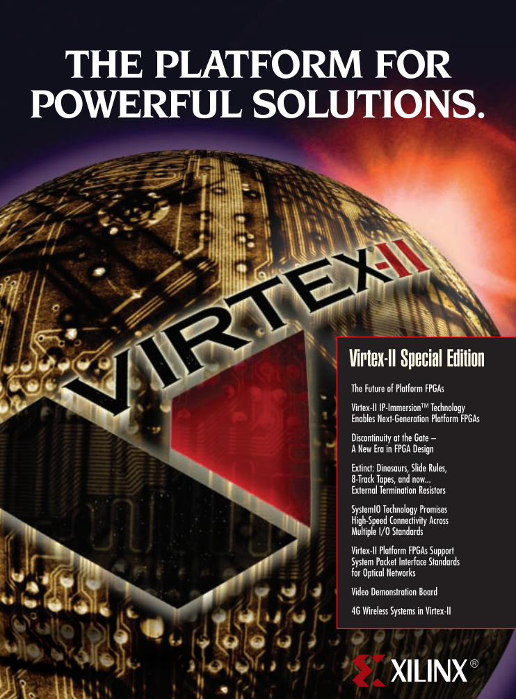
THE PLATFORM FOR POWERFUL SOLUTIONS.
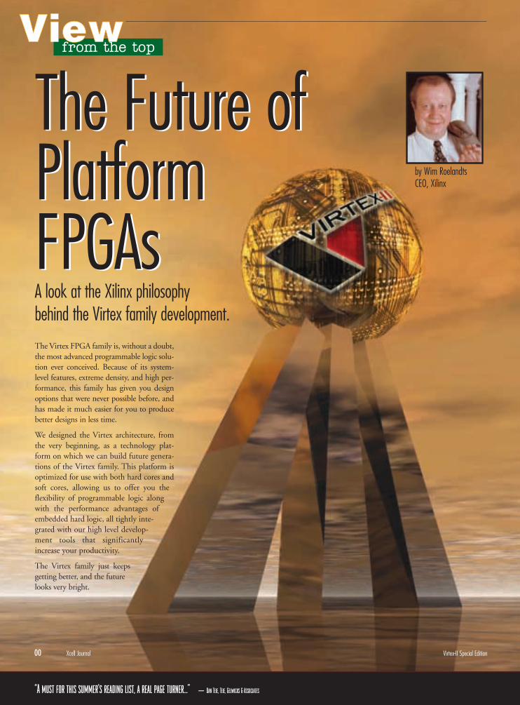
The Future of Platform FPGAs
Virtex-II IP-Immersion™ Technology Enables Next-Generation Platform FPGAs
Discontinuity at the Gate – A New Era in FPGA Design
Extinct: Dinosaurs, Slide Rules, 8-Track Tapes, and now... External Termination Resistors
SystemIO Technology Promises High-Speed Connectivity Across Multiple I/O Standards
Virtex-II Platform FPGAs Support System Packet Interface Standards for Optical Networks
Video Demonstration Board
4G Wireless Systems in Virtex-II
Virtex-II Special Edition

I N T R O D U C I N G I S E 4.1i
The fastest programmable design software just got fasterGet ready to fly. Our ISE 4.1i software release completes your design twice as fast as our previous generation, and up to 6
times faster than competitive tools. With an array of industry-unique features, ISE 4.1i gives you unbeatable performance
advantages, increasing your design’s clock performance by up to 75%, and enabling I/O speeds of 3.125 Gbits/sec.
Performance and Speed with ProActive™ Timing Closure ISE 4.1i features Xilinx ProActive Timing Closure - a set of new technologies including physical
synthesis integration, HDL analysis, timing wizards with cross-probing, and the most advanced
timing-driven place and route algorithms available in the industry today. This means ISE 4.1i will
intelligently identify, analyze, and solve any potential timing bottlenecks. Also, our new Directed
Routing technology delivers unprecedented improvements in performance
predictability for IP.
A single design environment for all Xilinx devicesCombine the superior performance of ISE 4.1i with the speed and density
leadership of the Virtex®-II Platform FPGAs, the Spartan®-II ASIC replacement FPGAs, the ultra-low
power CoolRunner™ CPLDs, plus our high-performance XC9500™ CPLDs. With the first and only
FPGA support for industry-leading formal verification tools, and clock speeds over 300MHz, Xilinx
provides the totally integrated design solution.
Visit www.xilinx.com/v2insert/swad today for all the speed you need!
The Programmable Logic CompanySM
www.xilinx.com/ise/xcell
©2001 Xilinx, Inc., 2100 Logic Drive, San Jose, CA 95124, U.S.: 408-559-7778, Europe: 44-870-7350-600, Japan: 81-3-5321-7771, Asia: 852-2-424-5200, Xilinx is a registered trademark, and The Programmable Logic Company is a service mark of Xilinx, Inc.
For more information visit xilinx.com/v2insert/swad
The Virtex FPGA family is, without a doubt,the most advanced programmable logic solu-tion ever conceived. Because of its system-level features, extreme density, and high per-formance, this family has given you designoptions that were never possible before, andhas made it much easier for you to producebetter designs in less time.
We designed the Virtex architecture, fromthe very beginning, as a technology plat-form on which we can build future genera-tions of the Virtex family. This platform isoptimized for use with both hard cores andsoft cores, allowing us to offer you theflexibility of programmable logic alongwith the performance advantages ofembedded hard logic, all tightly inte-grated with our high level develop-ment tools that significantlyincrease your productivity.
The Virtex family just keepsgetting better, and the futurelooks very bright.
A look at the Xilinx philosophy behind the Virtex family development.
The Future of Platform FPGAs
VViieewwfrom the top
by Wim RoelandtsCEO, Xilinx
The Future of Platform FPGAs
“A must for this summer’s reading list, a real page turner...” – Dan Teie, Teie, Gelwicks & Associates
00 Xcell Journal Virtex-II Special Edition
Performance Philosophy
Our first priority, with all of our devices, isto continuously improve the performance,density, and features. We work very closelywith our manufacturing partners to refineour manufacturing processes, creatingincreasingly smaller geometry CMOS tech-nologies that result in faster, denser devices,for less cost – we will introduce a new gen-eration every year with increasinglyadvanced process technology. In addition,we are continuously developing new waysto improve our device architectures, to getbetter performance through enhancedrouting and design features.
Today, you can purchase Virtex-II deviceswith up to 6 million system gates, a hugeadvancement in density over previousFPGAs. Yet, within three or four years wewill offer 50 million gate devices – enoughlogic to build very complex, very high per-formance systems, on a single chip. In addi-tion, Virtex-II devices now operate at inter-nal clock speeds above 200 Mhz, the equal ofmany custom ASICs. Yet, every year, for thenext four to five years, we expect a perform-ance increase of 30% to 50%. (The inherentsilicon performance increase is about 30%per year. Then, as we improve the routinginfrastructure and so on, we expect up toanother 20%.) As you can see, programma-ble logic technology is advancing very quick-ly, giving you more options, more capability,more flexibility, and more reasons to moveaway from ASICs and fixed logic designs.
The basic structure of an FPGA determinesnot only its capability and its ease of use, italso determines its ability to evolve as newtechnologies are developed and implement-ed. You want your FPGA family to growwith your needs without having to learn newtools, processes, and design techniques.That’s why we developed a flexible, highlypredictable, forward-thinking architecturethat can easily integrate custom logic, softcores, hard cores and mixed signal capability.
With the Virtex-II family you’ll not onlyachieve high performance, you’ll do itwith a high degree of predictability andfamily stability which is key to your pro-ductivity. Plus, migrating to larger deviceswith higher performance, as they aredeveloped, is easy.
Memory is a critical part of most designs.The ratio of memory to logic gates in theVirtex family will continue to increase overtime because our customers are demandingmore and more memory. The amount ofblock RAM and distributed RAM willincrease, as well as the ability to access off-chip memory – as memory standards evolve,so will our memory interface capability.
Clock management is another critical factorin large designs. The Virtex-II Delay LockedLoop Digital Clock Manager is already themost advanced, feature rich, clock managerin the industry. It eliminates clock skew, pro-vides very flexible clock synthesis capabilities,
and gives youthe ability todrive and syn-chronize clocksboth on and offchip, thus elimi-nating externalcomponents andsimplifying yourdesign. It willevolve as wedevelop evenmore advancedtechniques.
The embeddedmultipliers in the Virtex family
allow you to create the fastest possibleDSP designs. Our customers are achiev-
ing unprecedented speeds of well over 0.5TeraMACs (Multiply-Accumulate Cyclesper second). Many customers are pushingthe limits of performance and density intheir networking designs, requiring verysophisticated DSP algorithms to extract thedata from the noise. Because these hardcore multipliers are so useful, in a widerange of applications, they will be added toevery Virtex-family FPGA.
We will continue to develop hard and softcores that make full use of the Virtex familyarchitecture, to bring you all the ease-of-useand performance advantages that makePlatform FPGAs so attractive.
I/O Philosophy
Over the last few years we have madetremendous progress in the I/O capabilitiesof our devices. In the past, I/O blocks were
It all starts with a strong FPGA platform,tightly integrated with fast, high-level devel-opment tools – and there is no end in sightto where this family can go.
Core Philosophy As device densities keep increasing, itbecomes even more important that weprovide a wide range of intellectual prop-erty or cores, which help you quicklydevelop your design. Without cores, itwould take many engineer-years to com-plete a 8-million gate design. With coresyou can quickly create key parts of yoursystem using proven, reliable designs.
Our “platform” philosophy is toprovide both hard and softcores that take full advantage ofour Virtex architecture. Hardcores (such as the PowerPC) areactually fixed logic designs that we incorporate into the FPGA device architecture.Wherever possible,we’ll offer soft coresto solve yourdesign challengesbecause they aremore flexible andare used on an asneeded basis. We’lloffer hard coreswhen there is a per-formance or density advan-tage. The Virtex architecture allowsyou to easily integrate both types of coresinto your designs, giving you the maximumflexibility and performance
Hard Cores
As we move forward, we’ll integrate moreand more hard cores into our FPGA plat-form to increase the performance and easeof use. Examples include central proces-sors, memory blocks, clock managers,multipliers, and high speed I/O systems.
Processor cores save you a lot of develop-ment time and they give you a known,reliable design. Our philosophy is totightly integrate our processor cores intothe FPGA fabric so you can achievetremendous performance advantages thatwould not be available if you used a sepa-rate processor chip.
Viewfrom the top
Virtex-II Special Edition Xcell Journal 00
For more information visit xilinx.com/v2insert/wim
very standard, and they could usually sup-port just one voltage. Today with theVirtex-II family we support the vast major-ity of I/O standards in the industry. If youlook at a combination of different stan-dards and drive currents, we have 49 differ-ent ways that you can program every singleI/O pin. And we will continue to add newI/O capabilities as standards evolve.
High Speed Serial I/O
The demands of high speed network-ing, and other high perform-ance systems, requires theuse of gigabit-per-secondserial I/O capability forinterconnecting devices,backplanes, and sys-tems. In addition, someof the new communica-tions standards andbackplane standards arebased on these high speedserial I/O capabilities, includ-ing POS-PHY4, FlexBus4,HyperTransport™, InfiniBand™, FibreChannel, Gigabit Ethernet, and so on.With the Virtex-II I/O capability you canconnect directly to a backplane withoutexternal components.
Through our Conexant Skyrail™ licensingagreement, we gained access to the highestspeed I/O technology available – currentlygiving us a serial transceiver capability ofup to 3.125 Gbps. With our RocketChips®
acquisition, we expect our serial transceivertechnology to reach 10 Gbps or more, asour process and design technologies con-tinue to improve. Future Virtex familieswill allow you to make full use of thisimportant capability.
Processor Philosophy
We intend to offer you a choice of proces-sors using both hard and soft cores; allusing the same peripherals so you can easi-ly combine processors in your designs.
PowerPC Hard-Core Processor
Our PowerPC hard core is being developedin partnership with IBM. It gives you awell-known, very high performance archi-tecture. We will embed this processor with-in our programmable logic fabric, so all ofthe processor I/O pins are available to the
internal programmable logic for maximumflexibility. Plus, the processor I/O pins donot take up valuable FPGA I/O resources,unless you need them. This allows you tomove data much faster than the competi-tion. Our competition’s embedded proces-sor does not have the same performance orflexibility as our PowerPC core.
Our philosophy is to provide all of theperipherals and so on as soft cores so they
require no resources if you don’t needthem; we chose to provide the
PowerPC processor as ahard core because it
gives you a perform-ance advantage. AsIBM continues toimprove the per-formance of thePowerPC, Xilinx
will continue to offerthe latest PowerPC
processor core technolo-gy, optimized for the Virtex
architecture.
MicroBlaze Soft-Core Processor
Our MicroBlaze™ soft-core processor wasdeveloped by Xilinx. It uses only about800 logic cells, requires about the samephysical space as the PowerPC, and runs at125 Mhz. By next year, it will be runningat over 150 Mhz.
MicroBlaze is fully integrated with theCore Connect architecture of IBM whichmeans it can use the peripheral moduleswe’re developing for the PowerPC proces-sor. In fact, you can use it in addition to thepower PC processor. For example, you canhave a combination of the PowerPC andone or more MicroBlaze cores spreadaround it, all using the same memory andperipherals. The possibilities are limitless.
No other company has this flexible multi-processor capability. Plus, our MicroBlazesoft core runs almost as fast as our compe-tition’s hard core processor
Board Integration PhilosophyWith each new generation of the Virtexfamily we will integrate more and more ofthe discrete components that are required tocreate a working system, making your PCboards simpler and less expensive. Our goal
is to make our I/O structure so extensivethat you will never have to use glue logic orunderstand the intricacies of each new stan-dard. For example, by integrating a varietyof different memory interfaces into ourFPGAs, you can easily connect any knownmemory device without having to createyour own custom interface designs.
All of these trends will continue in the future– as new I/O standards are introduced, we’llmake them available on our FPGAs.
XCITE
The Xilinx Controlled ImpedanceTEchnology (XCITE) is another exam-ple of PC board simplification andimproved signal integrity. XCITE placesdigitally controlled termination resistorson the FPGA, so you don’t have to man-ually terminate your signals with hugenumbers of discrete external resistors.This not only saves you a lot of boardspace and cost, it makes board layoutmuch simpler. This built-in terminationadjusts itself for temperature and voltagevariations as well, so your boards are notonly less expensive, they are also morereliable. XCITE solves the signal integrityissues that both circuit and PCB design-ers are now dealing with, allowing you torun your PC boards at full speed and getthem to market quickly.
Conclusion Our FPGAs add more than just logic; theyare tremendously more valuable because,they make your design simpler, they elimi-nate other components on your board, andthey continue to decrease your develop-ment time and costs.
If you want to build the systems of thefuture, and keep your costs down, you needa solid foundation on which your designs cangrow and evolve as technology advances. Youneed a logic solution that will grow with youand help you solve the problems that haveyet to be encountered. You need the devices,software tools, and company support thatmake a complete solution. That’s what youget with the Xilinx Virtex-II Platform FPGAfamily. It’s already the industry leader, by far,and it just keeps getting better.
I hope you enjoy this Special Virtex-IIsupplement.
22 Xcell Journal Virtex-II Special Edition
Viewfrom the top
“A must for this summer’s reading list, a real page turner...” – Dan Teie, Teie, Gelwicks & Associates
00 Xcell Journal Virtex-II Special Edition
The Field Programmable Gate ArrayRevolution began when Ross Freeman, afounder of Xilinx, conceived the FPGAarchitecture. Abandoning the restrictions ofsum-of-products architecture, Ross utilized ahost of 16-bit LUTs (Look-Up-Tables), eachaccompanied by a flip-flop circuit, and allinterconnected with programmable routingpathways. This revolutionary formula, firstdeployed in 1984 in the Xilinx XC2000 fam-ily, is still the basis of all FPGA devices today,despite the unprecedented growth in thescale of programmable logic and continualadvances in the complexity of the devicearchitecture. It is a testament to the power ofRoss’s architectural vision that the FPGA haswithstood the test of time, and many pro-posed alternatives in the marketplace.
Perspective Platform FPGAs
Virtex-II IP-Immersion™
Technology Enables Next-Generation Platform FPGAs
Innovative technology allows the integration of discrete siliconcomponents within Platform FPGAs.
by Erich GoettingVice President, Product Development, [email protected]
“A must for this summer’s reading list, a real page turner...” – Dan Teie, Teie, Gelwicks & Associates
00 Xcell Journal Virtex-II Special Edition
Perspective Platform FPGAs
Introducing the Revolutionary Platform FPGA
Today, in 2001, however, another revolu-tion in programmable logic has begun withthe introduction of Xilinx Virtex®-IIPlatform FPGAs. At the heart of this rev-olution is the ability to integrate the func-tions of other discrete silicon devices,such as microprocessors, within an FPGAplatform. The integration provided by thePlatform FPGA architecture deliversthese advantages:
• Increased performancemade possible by high-bandwidth, low-latencycoupling of intellectualproperty (IP) blocks
• Enhanced architecturalflexibility by virtue ofimmersion within a high-performance program-mable fabric
• Reduced board space,power, and cost.
Although Platform FPGAsrepresent a revolutionarystep forward, they stillretain the fundamentaladvantages over ASICs(Application SpecificIntegrated Circuits) –namely, reprogrammabili-ty, off-the-shelf availabili-ty, and zero non-recurringengineering (NRE) costs.These advantages com-prise the infrastructurethat has enabled the devel-opment of the innovative IP-Immersionsuperstructure.
Enhanced Performance Through IP-Immersion
The Virtex-II IP-Immersion™ architec-ture embodies the concept that high-bandwidth, hard-IP blocks – implement-ed in full-custom or ASIC-style standardcell logic – can be immersed within thematrix of FPGA CLBs (ConfigurableLogic Blocks). The two-dimensional arrayof Virtex-II CLBs is ideally suited for thistask, because the array possesses three all-important properties:
interconnect with the logic, memory,and I/Os of the FPGA platform. Toprovide the transition between theplatform fabric and the hard-IP,Virtex-II devices introduce a new tiletype: an “immersion tile.” The immer-sion tile allows programmable inter-connections between the IP-block andthe fabric – much like the interconnec-tion of discrete devices on a printedcircuit board. For example, a designer
can instantiate a large blockand wire it to other parts ofthe system. In wiring thisblock, the designer canchoose to connect an out-put pin to a net, leave anoutput unconnected, tieinputs to fixed one or zerolevels, or connect an inputto a particular net. In thisway, the designer has fulldesign flexibility in usingIP blocks.
3. High performance func-tionality – The highwiring density and fullyactive nature of theVirtex-II routing archi-tecture allows connec-tions to occur in largequantities and at highspeed, thus enabling thehigh-bandwidth inter-connect necessary tofully exploit the poten-tial of on-chip IP blocks.
Taken together, these threeproperties constitute the key ingredientsof the new Virtex-II IP-Immersionarchitecture.
Conclusion
The Virtex-II series of Platform FPGAsare engineered to provide leading-edgefunctionality in logic, routing, clocking,DSP, memory, and I/O. Thanks to theinnovative IP-Immersion architecture anddevelopment relationships with leadingcompanies such as IBM, Xilinx Virtex-IIPlatform FPGAs are facilitating the nextgeneration of advanced system designs.
1. Configurable layout – Because hard-IP blocks (such as microprocessors)have a particular shape, the designercan “cut out” just the right amount ofCLBs, creating an empty space for theIP-block. As a result, high performancehard-IP blocks, such as the IBMPowerPC 405 32-bit RISC CPU, canbe implemented using advanced circuitdesign and layout techniques that max-imize performance and minimize sili-
con area. The Virtex-II IP-Immersionarchitecture accommodates virtuallyany pre-defined rectilinear shape.
2. Programmable routing – Through itsstep-and-repeat of CLB tiles, the seg-mented routing of FPGA architectureallows the creation of specific “on-ramps” and “off-ramps” at every CLBborder. In other words, because theVirtex-II routing architecture has somewiring segments that start within everyCLB, these starting segments providean ideal way for the hard-IP block to
Hard IPH CoreConnectCSoft IPS
IP-Immersion Technology
Virtex-II Special Edition Xcell Journal 00
For more information visit xilinx.com/v2insert/erich
“A must for this summer’s reading list, a real page turner...” – Dan Teie, Teie, Gelwicks & Associates
00 Xcell Journal Virtex-II Special Edition
by Walden C. RhinesChairman and CEO, Mentor Graphics [email protected]
What happens when you give the designcommunity a field-programmable hardwareplatform that contains 8 million systemgates, 300+ MHz internal clock speeds,gigabit serial I/O performance, and IPimmersion technology? You create an oppor-tunity for an entirely new complex designmethodology. By providing such robustcapabilities in a programmable format, youcreate a discontinuity in the industry thatremoves previous cost and technology barri-ers from the product development process.The Xilinx Virtex-II Platform FPGA familyembodies this emerging technology, and hasprovided the catalyst to change our currentdesign methodologies.
Today it is estimated that there are 20,000custom or semi-custom chip designers, andthis number is growing very slowly, as shownin Figure 1. Under the current structure,issues including design styles, verificationmethodologies, NRE charges, risk, and soft-ware development inhibit how many circuitscan be attempted each year. Creating a stan-dard platform for development removesthese limitations, and allows the number ofpotential designers to grow by an order ofmagnitude, to 200,000. This massive influxof potential designers creates a new brainpool for innovation.
The Xilinx vision in programmable logic will change how youdo digital design. Mentor Graphics has recognized this and iscommitted to the FPGA market.
Discontinuity at the Gate – A NewEra in FPGA Design
Cover StoryMentor Graphics CEO
Discontinuity at the Gate – A NewEra in FPGA DesignThe Xilinx vision in programmable logic will change how youdo digital design. Mentor Graphics has recognized this and iscommitted to the FPGA market.

For more information visit xilinx.com/v2 insert/mentor
Cover Story Mentor Graphics CEO
FPGAs Coming of Age
The path to harmonybetween design tools andactual silicon is extremelychallenging. For example, asshown in Figure 2, in theASIC world it took 15 yearsto merge the silicon processwith a solid design method-ology based on reliable andfunctional EDA software.ASIC technology became thedriving force in the industry.The process that began sur-rounding this technologycreated an effective solutionfor the electronics industry,which led to growth andinnovation. But the ASICprocess has matured to thepoint where it is applicablemore for extremely high-enddesign, and it is slowly mov-ing out of reach for the massmarket.
In contrast, FPGA technolo-gy has taken only five yearsto get to the same level offunctionality as ASICs.FPGA technology hasuniquely solved the sameproblems the ASIC method-ology addressed, but alongthe way it also minimizedthe NRE, risk, and manufac-turing issues involved asillustrated in Figure 3.Today, the Xilinx Virtex-IItechnology is a legitimateASIC replacement. Whencombined with leading-edgeEDA software, Virtex-IIFPGAs provide the electron-ics industry with a new,exciting path for growth andinnovation. FPGAs are nowthe key vehicle driving thestate-of-the-art for new elec-tronic systems.
The Xilinx platform-basedFPGA technology brings pro-
grammability to the System-on-Chip (SoC) methodology.Using a 0.15µ, 8-layer metalprocess with 0.12µ high-speedtransistors, Virtex-II FPGAsprovide designers with theperformance and density theyneed to create an SOC design.With features like digitalclock management, select I/Oultra technology, and activeinterconnect, designers canspend more time on function-al verification, knowing thatthe main silicon issues andproblems have already beensolved. In addition, with IPimmersion technology, FPGAdesigners can now work at amuch higher level of abstrac-tion and move the “gates per day” metric to a levelwhere silicon utilization ismaximized.
Platform-Based FPGAs –The Value of History
Creating standards and put-ting boundary conditions ona design process can acceleratecircuit development andshorten time to market. TheASIC SOC developmentprocess in place today is anopen-ended approach todesign with almost an infinitedegree of freedom. This free-dom provides flexibility andhas enabled the creation ofextremely complicated cir-cuits, but it has also created ahigh risk methodology with asteep learning curve.
In contrast, platform-basedFPGAs provide a structuredapproach to design. From thedesigner’s point of view, thebeauty of creating an FPGA isthat the FPGA vendors worryabout all the issues of thedesign process (silicon,methodology, and software).
Custom IC Designers (Slide 5)
Gat
es P
er C
hip
100,000,000
10,000,000
1,000,000
100,000
10,000
1,000
100
10
1
1980
1982
1984
1986
1988
1990
1992
1994
1980
1996
1999
2001
2003
2005
2007
2009
~2000
~20,000
~200,000
Figure 1 - Gate-to-designer ratio
Figure 2. Evolution of ASIC and FPGA design methodologies
CumulativeNRE+Unit Cost
CumulativeVolume K Units
ASIC CostsStart higher,but slope isflatter.
For each technology advance,PLDs become more cost effective.
ASIC .15µ
ASIC .25µ
PLD .25µ
PLD .15µ
Figure 3. FPGA to ASIC crossover improves with process
Virtex-II Special Edition Xcell Journal 00

“A must for this summer’s reading list, a real page turner...” – Dan Teie, Teie, Gelwicks & Associates
00 Xcell Journal Virtex-II Special Edition
Cover Story Mentor Graphics CEO
From the FPGA vendor’s point of view,they need to provide their customers witha solution that enables high-quality,repeatable results.
Platform-based FPGAs have taken theproblems found by previous ASIC SoCdesigners and minimized them by pro-
viding a proven, recommended path forsuccess. In the history of electronicdesign, innovation and productivity areat their peak when proven methodologiespermeate the industry.
IP Immersion
Designing an ASIC SoC requires a highlyexperienced team of engineers from mul-tiple disciplines. This team must learnhow to use a processor, develop softwareon it, and connect IP into the system.These learning curves are long and riddled
with mistakes. And, because all designblocks come from different places, inte-gration rarely works on the first try.
Platform-based FPGAs solve some of thebig issues that limit the development of
ASIC SoCs by addressing IPintegration issues, as shownin Figure 4. The Xilinx IPimmersion technology max-imizes performance anddensity by providing a fixedand proven structure tointegrate hard and soft IPinto the silicon architecture.
Platform-based FPGAsusing embedded processorswill be the next key tech-nology that will pushFPGA design forward. Bylimiting support to onlycertain CPU architectures,all integration informationis predefined for functionssuch as control signals,clocks, and data buses. SoftIP is pre-engineered towork with these pre-defined buses, so thedesigner just needs to con-nect these fixed IP objectsto the buses. For the user-
defined section of the chip, the designhas been made easier because its bound-ary conditions are known.
To take advantage of these fixed-CPUplatform-based FPGAs, designers willlook for new applications and uses. Sincethe cost of implementation will be ineveryone’s reach, we should see a resur-gence of the garage-shop mentality andnew out-of-the-box thinking.
Enabling Innovation Together
At Mentor Graphics, we enjoy collaborat-ing with a partner that looks at the bigpicture and asks, “How do I change thefuture?” The Xilinx vision in programma-ble logic will change how we do digitaldesign. Mentor has recognized this and iscommitted to the FPGA market. We con-tinue to develop point tools and solutionsto solve the tough design problems.Mentor realizes that dedicated FPGAflows, tested and integrated tightly withthe vendor software, will provide the tech-nology that will “Enable Innovation” forthe future of the electronic industry.
Figure 4 - Platform-based FPGAs integrate IP to user-defined logic
Today, the Xilinx Virtex-II technology is a legitimate ASIC replacement.
When combined with leading-edge EDA software, Virtex-II FPGAs provide the
electronics industry with a new, exciting path for growth and innovation.— Walden C. Rhines, Chairman and CEO, Mentor Graphics
by Mark AlexanderProduct Applications Engineer, Xilinx [email protected]
Termination resistors as we know them areabout to vanish. XCITE (Xilinx ControlledImpedance TEchnology) – the adaptiveon-chip termination system now availablein the Virtex®-II family of FPGAs – ban-ishes external resistors, making PCBs(Printed Circuit Boards) less expensive, eas-ier to design, and more reliable.
High performance systems require signalfrequencies in the hundreds of megahertz,necessitating impedance matchingbetween device I/Os and PCB traces. Inthe past, as clock speeds increased and I/Ostandards changed, system engineers andPCB designers learned signal terminationtechniques, using external resistors tomatch impedances. Over time, more andmore resistors were required to accountfor the increasing widths of large databusses. With the advent of 1,500-pinpackages, discrete resistor placementbecame a major challenge.
External termination resistors necessitatemore board traces and increased PCB partcounts, making the layout process moretime consuming. These factors lead tohigher manufacturing costs and longertimes to market. Additionally, sky-highpart counts do not help system reliabilityeither – each additional part increases therisk of a system failure.
Here at Xilinx, our Virtex-II team wanteddesigners to have a worry-free solution toterminating high-speed signals, so weinvented XCITE I/O. All Virtex-II I/O pinsare equipped with XCITE, making imped-ance matching a pre-engineered solution.
Technology XCITE
Xilinx Virtex-II Platform FPGAs
now feature the world’s first
on-chip digitally controlled
impedance-matching technology.Extinct: Dinosaurs, Slide Rules, 8-Track Tapes, and now... ExternalTermination Resistors
Extinct: Dinosaurs, Slide Rules, 8-Track Tapes, and now... ExternalTermination Resistors
“A must for this summer’s reading list, a real page turner...” – Dan Teie, Teie, Gelwicks & Associates
00 Xcell Journal Virtex-II Special Edition
Technology XCITE
XCITE can be used to terminate a varietyof I/O standards. All variants of HSTL (High-Speed Transistor Logic), SSTL (StubSeries Terminated Logic), GTL (GunningTransceiver Logic), and LVCMOS (LowVoltage Complementary Metal OxideSemiconductor) are supported. Designers
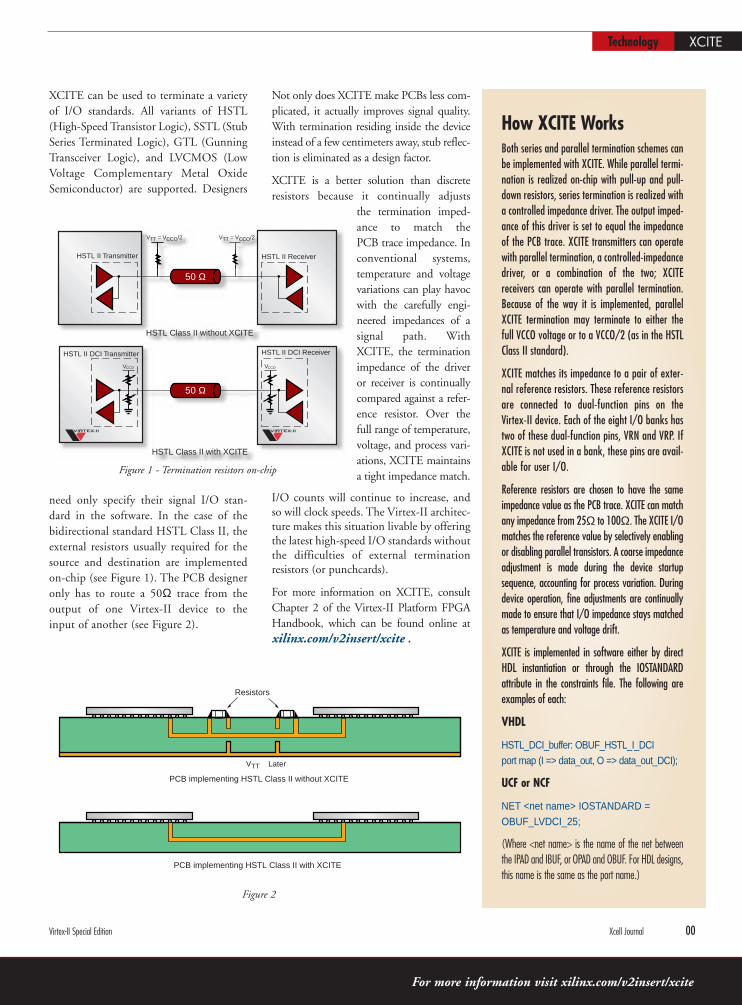
need only specify their signal I/O stan-dard in the software. In the case of thebidirectional standard HSTL Class II, theexternal resistors usually required for thesource and destination are implementedon-chip (see Figure 1). The PCB designeronly has to route a 50Ω trace from theoutput of one Virtex-II device to theinput of another (see Figure 2).
Not only does XCITE make PCBs less com-plicated, it actually improves signal quality.With termination residing inside the deviceinstead of a few centimeters away, stub reflec-tion is eliminated as a design factor.
XCITE is a better solution than discreteresistors because it continually adjusts
the termination imped-ance to match the PCB trace impedance. Inconventional systems,temperature and voltagevariations can play havocwith the carefully engi-neered impedances of asignal path. WithXCITE, the terminationimpedance of the driveror receiver is continuallycompared against a refer-ence resistor. Over thefull range of temperature,voltage, and process vari-ations, XCITE maintainsa tight impedance match.
I/O counts will continue to increase, andso will clock speeds. The Virtex-II architec-ture makes this situation livable by offeringthe latest high-speed I/O standards withoutthe difficulties of external terminationresistors (or punchcards).
For more information on XCITE, consultChapter 2 of the Virtex-II Platform FPGAHandbook, which can be found online atxilinx.com/v2insert/xcite .
How XCITE WorksBoth series and parallel termination schemes canbe implemented with XCITE. While parallel termi-nation is realized on-chip with pull-up and pull-down resistors, series termination is realized witha controlled impedance driver. The output imped-ance of this driver is set to equal the impedanceof the PCB trace. XCITE transmitters can operatewith parallel termination, a controlled-impedancedriver, or a combination of the two; XCITEreceivers can operate with parallel termination.Because of the way it is implemented, parallelXCITE termination may terminate to either thefull VCCO voltage or to a VCCO/2 (as in the HSTLClass II standard).
XCITE matches its impedance to a pair of exter-nal reference resistors. These reference resistorsare connected to dual-function pins on theVirtex-II device. Each of the eight I/O banks hastwo of these dual-function pins, VRN and VRP. IfXCITE is not used in a bank, these pins are avail-able for user I/O.
Reference resistors are chosen to have the sameimpedance value as the PCB trace. XCITE can matchany impedance from 25Ω to 100Ω. The XCITE I/Omatches the reference value by selectively enablingor disabling parallel transistors. A coarse impedanceadjustment is made during the device startupsequence, accounting for process variation. Duringdevice operation, fine adjustments are continuallymade to ensure that I/O impedance stays matchedas temperature and voltage drift.
XCITE is implemented in software either by directHDL instantiation or through the IOSTANDARDattribute in the constraints file. The following areexamples of each:
VHDL
HSTL_DCI_buffer: OBUF_HSTL_I_DCI port map (I => data_out, O => data_out_DCI);
UCF or NCF
NET <net name> IOSTANDARD =OBUF_LVDCI_25;
(Where <net name> is the name of the net betweenthe IPAD and IBUF, or OPAD and OBUF. For HDL designs,this name is the same as the port name.)
HSTL II Transmitter
HSTL Class II without XCITE
HSTL II Receiver
50 Ω
HSTL II DCI Transmitter
HSTL Class II with XCITE
HSTL II DCI Receiver
50 Ω
V CCO V CCO
VTT = VCCO/2 VTT = VCCO/2
PCB implementing HSTL Class II without XCITE
VTT Later
Resistors
PCB implementing HSTL Class II with XCITE
Figure 1 - Termination resistors on-chip
Figure 2
Virtex-II Special Edition Xcell Journal 00
For more information visit xilinx.com/v2insert/xcite
by Rina RamanAPG Director of Applications Engineering, [email protected]
Moore’s Law, which predicts computerprocessor speeds will double approximatelyevery 18 months, has proved to be remark-ably accurate for more than 35 years. Theexponential increases in processor speedshave enabled ever higher bandwidth net-working. The problem now, however, isthat I/O busses have only doubled their fre-quencies every three years. Thus, the level ofperformance of a system at the board level isnow dictated not by the speed of processorbut by the limits of the I/O bus. Whiledelivering greater bandwidth, numerousemerging I/O standards – RapidIO™,POS-PHY™ Level 4, 10 Gb/s Ethernet,XAUI, HyperTransport™, Fibre Channel,among others – provide various choices andarchitectural options. Xilinx Virtex®-IIPlatform FPGAs address this proliferationof standards with the SystemIO™ solution,which provides system interconnectivity atboth the physical I/O interface and the net-working protocol levels.
I/O Signaling Standards
Virtex-II devices are designed to supportmany signaling standards, including essen-tial interfaces to high performance systems.For instance, memory devices operatingabove 180 MHz can only use SSTL (StubSeries Terminated Logic) or HSTL (HighSpeed Transceiver Logic) I/O standards.
Many I/O standards – including the tradi-tional switching standards of LVCMOS(Low Voltage CMOS), memory interfacesof HSTL and SSTL, and even LVDS (LowVoltage Differential Signaling) – are notkeeping pace with the increased demandfor more bandwidth. Designers have triedto overcome these bandwidth limits byusing more pins and/or larger bus widths.This has made the traditional I/O stan-dards more “pin-intensive.” Significantproblems arise as pin counts grow into thehundreds and thousands, creating routingcongestion on printed circuit boards.Although Virtex-II Platform FPGAs caneasily route inside the device, it is extreme-ly difficult to interface with all the pins ona PCB. More layers of interconnect rout-ing in the PCB cause dramatic increases inoverall board costs. The number of pinsrunning these standards also producesproblematic electromagnetic interference.
Additionally, the most popular bus archi-tecture is a “shared” medium where mul-tiple entities use the same bus, each wait-ing in turn for its opportunity to com-plete its transaction. As the size of audioand video data streams increase, the wait-ing period gets longer. Ultimately, overallperformance decreases along with per-formance predictability. Therefore, theindustry trend is to move from a sharedbus to a point-to-point link, typicallyconfigured as a switched fabric.
Beyond the Shared PCI Bus
The most popular shared bus is the PCI(Peripheral Component Interconnect) bus.It has become a general-purpose bus forpersonal computers and embedded sys-tems supporting many different applica-tions. A 33 MHz, 32-bit PCI bus can sup-port one source and five destinations withan overall bandwidth of 1 Gb/s. At 66MHz and 64 bits, the bandwidth rises to 4Gb/s, but then the bus only supports onesource and two destinations. The PCIshared bus structure has diminishing per-formance returns, is less predictable than apoint-to-point solution, and is limited tointernal systems.
Ideally, we would like to establish a linkand then “burst” the data over a reallywide data bus. This would maximize busefficiency. Bus efficiency is highest withlong bursts.
Decreased bus efficiency has many causes.Although we may have economies of scalefor most applications, the shared PCI buscompromises graphics performance. Forexample, when using a PCI graphics card,the graphics card needs to refresh every fewmilliseconds. In order to do this, it needs tohave immediate and frequent access to thePCI bus. As a result, other PCI cards cannotsend huge data bursts. This is because thePCI arbiter is designed to ensure that no onecomponent can send large bursts of data.
Innovations Networking
As implemented via Virtex-II Platform FPGAs, SystemIO technology addresses boththe physical interfaces and networking protocols for high bandwidth connectivity and throughput.
SystemIO Technology Promises High-Speed Connectivity Across Multiple I/O Standards
“A must for this summer’s reading list, a real page turner...” – Dan Teie, Teie, Gelwicks & Associates
00 Xcell Journal Virtex-II Special Edition

Innovations Networking
In graphics intensive applications, an AGP(Advanced Graphics Port) is a much betterchoice than a PCI bus. Although AGP isbased on PCI technology, it is designedespecially for the high throughput require-ments of 3D graph-ics. Rather thanusing the sharedPCI bus for graphicsdata transmission,the AGP introducesa dedicated point-to-point channel sothat the graphicscontroller candirectly access mainmemory. Virtex-IIPlatform FPGAssupport both PCIand AGP I/O stan-dards, as well asmany others.
Another drawbackof the PCI bus isthat it has no termi-nation – or rather, it is series terminated.This means that it relies on reflective waveswitching. Although reflective wave switch-ing is inexpensive and has relatively lowpower consumption, series terminationrequires the system to wait for the reflec-tion, so we lose valuable time.
Switched Fabric Advantages
A switched fabric is more scalable for highperformance and ultimately, offers a lowercost solution for high bandwidth applica-tions. In the past, data rates weren’t highenough to warrant using a switched fabricwithin a system, because this would requiremany point-to-point connections andwould increase system complexity. Withthe dramatic increases in performanceenabled by the new interface standards,however, switched fabric solutions arebecoming cost-effective.
With the huge existing PCI infrastructure,bridges are needed to interconnect the var-ious high-performance I/O standards.Virtex-II Platform FPGAs are key buildingblocks in the transition from shared busesto switched fabrics. The Virtex-II architec-
4) – This standard is defined for 10Gb/s Ethernet applications and opticalnetworking applications demandingOC-192 performance.
• 10 Gb/s Ethernet – Using an XGMIIinterface, this IEEEstandard is positionedto drive the conver-gence of LAN andWAN technologies.
In addition, there areemerging serial chan-nel standards as well.Two of the most pop-ular standards in thisarena are:
• Fibre Channel – Afavorite for the stor-age area networking(SAN) market, FibreChannel uses opticalfiber, coaxial cable,and/or twisted-pairtelephone wire.
• XAUI (pronounced ZOW-ee) – Thisnew standard targets 10 Gb/s serialchannels by bonding four 3.125 Gb/stransceivers. XAUI targets the OC-192and 10 Gb/s Ethernet markets for WANand LAN routers.
Conclusion
Having a solution that supports all these var-ious system interfaces is crucial to success inthe marketplace. The Virtex-II PlatformFPGAs’ SystemIO solution offers exactlythis – support for physical interfaces as wellas cores that support the network protocolsfor all the common and emerging systemI/O interfaces. Virtex-II FPGAs enable highperformance interfaces to memories fromCypress, IDT, Micron, SiberCore, GSITechnology and others, as well as interfacesto networking ASSPs (Application SpecificStandard Parts) from vendors such asAMCC, PMC Sierra, and Vitesse. Now,with Virtex-II SystemIO solution, you canpick any standard, and any vendor offeringthat standard in their ASSPs, and restassured that Xilinx Virtex-II PlatformFPGAs will support that standard.
ture supports universal switching capabili-ties to these new standards, making themthe logical choice for system designers.
As we mentioned earlier, the key advan-tage of SystemIO technology is that it
provides both physical interfaces as wellas various cores that support the networkprotocols. With the transition fromshared busses to switched fabrics comes avariety of different source-synchronous(parallel) protocols. The following aresome of the leading source-synchronousstandards that are emerging:
• RapidIO – Originally organized to sup-port the processor and local bus markets,the RapidIO interconnect architecturehas been embraced by the networkingand storage markets.
• InfiniBand™ – Founded by an industryconsortium, InfiniBand targets remotestorage, servers, and networking devices.
• HyperTransport – Formerly known asLDT (Lightning Data Transport),HyperTransport was jointly developed byAMD and API to replace PCI in high-speed computing applications. It hasgained some acceptance in the network-ing space.
• OIF - SPI4 (Optical InternetworkingForum - System Packet Interface Level
System-SynchronousParallel
AdvancedMemory
Interfaces
•• PCI-66• PCI-6CI-64/66• PCI-X13333
• ZBT SSRAM• SDRAM DDR SDRA• QDR SSRAMQD• CAM
Source-SynchronousParallel
• RapidIORapidIO• LDT• SPI-4• POS-PHY3• POS-PHY4• FlexBus3• FlexBus4• XGMII
Multi-GigabitSerial*
• Multi-Gigabit Backplanes Multi-Gigabi• InfiniBand• Gigabit Ethernet• 10 Gigabit Ethernet - XAUI• Fibre Channel
*Available in next generation
Virtex-II Special Edition Xcell Journal 00
For more information visit xilinx.com/v2insert/sysIO
by Ron DiGiuseppe System Interfaces Product Marketing Manager, [email protected]
Chris EbelingSystem Logic and Networking Staff Enginee, [email protected]
Xilinx has developed a suite ofLogiCORE™ intellectual property blocks toperform the System Packet Interface (SPI)function between the Physical (PHY) andData Link layer devices for POS/SDH(Packet Over SONET/Synchronous DigitalHierarchy) fiber optic applications. Thecores address the exploding demands of net-work IP (Internet Protocol) traffic by ensur-ing Xilinx devices are compatible with theOptical Internetworking Forum’s (OIF) SPI-4 Phase 2 standard as well as the SATURN®
Development Group POS-PHY™ Level 4(PL4) interface. The cores assure compli-ance with the OC-192 data transfer stan-dard by moving IP packets at a data rate inexcess of 10Gb/s.
Just in Time to Market
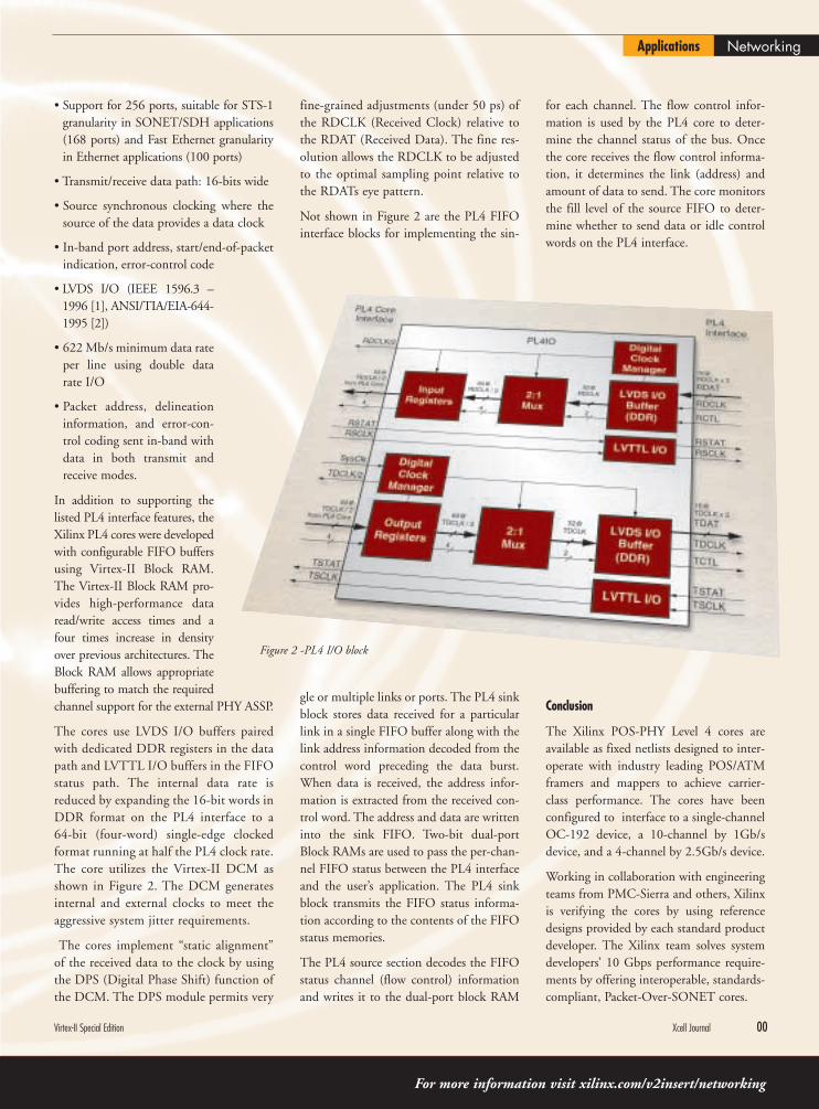
The interface cores, referred to as PL4 cores,make use of unique features available only inthe Xilinx Virtex™-II Platform FPGA archi-tecture – including DCM (Digital ClockManager), enhanced Block RAM, and high-speed LVDS I/O buffers. Combined withPlatform FPGA DDR (Double Data Rate)registers, the PL4 cores can support data ratesup to 832Mb/s per pin pair.
Xilinx is working with the OIF and theATM (Asynchronous Transfer Mode)Forum to promote the SPI-4 Phase 2 stan-dard. Along with other industry-leading net-working developers Xilinx is facilitating thedesign and deployment of data switchingand routing products using interoperableoptical networking technologies. Theimproved efficiencies and lower cost perMbit of POS/SDH packet transfer makes itan enabling technology for gigabit routers,terabit and optical cross-connect switches,and a wide range of multi-serv-ice DWDM (Dense WaveDivision Multiplexing) andSONET/SDH-based transmis-sion systems. The PL4 coresimplemented in Virtex-IIFPGAs allow next-generationnetwork developers to reducetheir system time to market.
In addition to providing fullystandard-compliant cores,Xilinx is collaborating withleading network device devel-opers – including PMC-Sierra, AMCC, andConexant – to ensure interoperabilitybetween the Xilinx networking cores and thelatest industry products. By combining theleading-edge performance of Virtex-IIdevices, Xilinx PL4 cores, and PMC-Sierra’sor Conexant’s OC-192 PHY devices, a com-plementary solution is available to ourmutual customers. With IP traffic on net-
work backbones doubling every six to ninemonths, it is critical to provide a high per-formance, scalable, system solution.
Interfacing the PHY and Data Link Layers
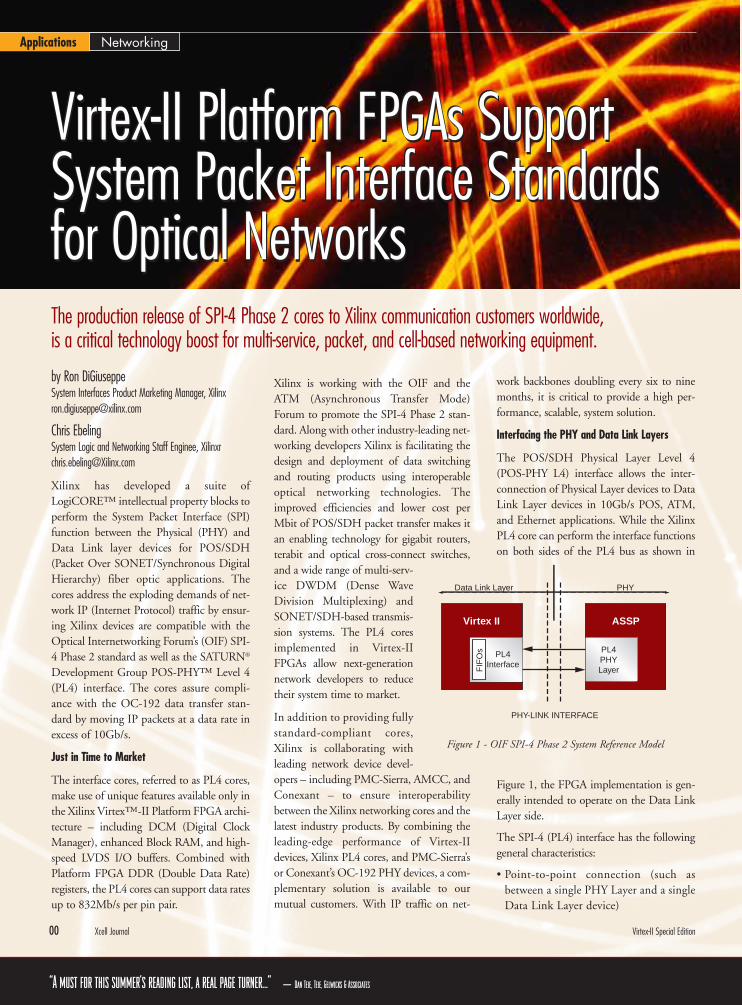
The POS/SDH Physical Layer Level 4(POS-PHY L4) interface allows the inter-connection of Physical Layer devices to DataLink Layer devices in 10Gb/s POS, ATM,and Ethernet applications. While the XilinxPL4 core can perform the interface functionson both sides of the PL4 bus as shown in
Figure 1, the FPGA implementation is gen-erally intended to operate on the Data LinkLayer side.
The SPI-4 (PL4) interface has the followinggeneral characteristics:
• Point-to-point connection (such asbetween a single PHY Layer and a singleData Link Layer device)
Applications Networking
The production release of SPI-4 Phase 2 cores to Xilinx communication customers worldwide, is a critical technology boost for multi-service, packet, and cell-based networking equipment.
Virtex-II Platform FPGAs SupportSystem Packet Interface Standards for Optical Networks
Data Link Layer PHY
Virtex II ASSP
PHY-LINK INTERFACE
PL4PHYLayer
PL4InterfaceF
IFO
s
Figure 1 - OIF SPI-4 Phase 2 System Reference Model
Virtex-II Platform FPGAs SupportSystem Packet Interface Standards for Optical Networks
Virtex-II Platform FPGAs SupportSystem Packet Interface Standards for Optical Networks
“A must for this summer’s reading list, a real page turner...” – Dan Teie, Teie, Gelwicks & Associates
00 Xcell Journal Virtex-II Special Edition
Applications Networking
• Support for 256 ports, suitable for STS-1granularity in SONET/SDH applications(168 ports) and Fast Ethernet granularityin Ethernet applications (100 ports)
• Transmit/receive data path: 16-bits wide
• Source synchronous clocking where thesource of the data provides a data clock
• In-band port address, start/end-of-packetindication, error-control code
• LVDS I/O (IEEE 1596.3 –1996 [1], ANSI/TIA/EIA-644-1995 [2])
• 622 Mb/s minimum data rateper line using double datarate I/O
• Packet address, delineationinformation, and error-con-trol coding sent in-band withdata in both transmit andreceive modes.
In addition to supporting thelisted PL4 interface features, theXilinx PL4 cores were developedwith configurable FIFO buffersusing Virtex-II Block RAM.The Virtex-II Block RAM pro-vides high-performance dataread/write access times and afour times increase in densityover previous architectures. TheBlock RAM allows appropriatebuffering to match the requiredchannel support for the external PHY ASSP.
The cores use LVDS I/O buffers pairedwith dedicated DDR registers in the datapath and LVTTL I/O buffers in the FIFOstatus path. The internal data rate isreduced by expanding the 16-bit words inDDR format on the PL4 interface to a64-bit (four-word) single-edge clockedformat running at half the PL4 clock rate.The core utilizes the Virtex-II DCM asshown in Figure 2. The DCM generatesinternal and external clocks to meet theaggressive system jitter requirements.
The cores implement “static alignment”of the received data to the clock by usingthe DPS (Digital Phase Shift) function ofthe DCM. The DPS module permits very
for each channel. The flow control infor-mation is used by the PL4 core to deter-mine the channel status of the bus. Oncethe core receives the flow control informa-tion, it determines the link (address) andamount of data to send. The core monitorsthe fill level of the source FIFO to deter-mine whether to send data or idle controlwords on the PL4 interface.
Conclusion
The Xilinx POS-PHY Level 4 cores areavailable as fixed netlists designed to inter-operate with industry leading POS/ATMframers and mappers to achieve carrier-class performance. The cores have beenconfigured to interface to a single-channelOC-192 device, a 10-channel by 1Gb/sdevice, and a 4-channel by 2.5Gb/s device.
Working in collaboration with engineeringteams from PMC-Sierra and others, Xilinxis verifying the cores by using referencedesigns provided by each standard productdeveloper. The Xilinx team solves systemdevelopers’ 10 Gbps performance require-ments by offering interoperable, standards-compliant, Packet-Over-SONET cores.
fine-grained adjustments (under 50 ps) ofthe RDCLK (Received Clock) relative tothe RDAT (Received Data). The fine res-olution allows the RDCLK to be adjustedto the optimal sampling point relative tothe RDATs eye pattern.
Not shown in Figure 2 are the PL4 FIFOinterface blocks for implementing the sin-
gle or multiple links or ports. The PL4 sinkblock stores data received for a particularlink in a single FIFO buffer along with thelink address information decoded from thecontrol word preceding the data burst.When data is received, the address infor-mation is extracted from the received con-trol word. The address and data are writteninto the sink FIFO. Two-bit dual-portBlock RAMs are used to pass the per-chan-nel FIFO status between the PL4 interfaceand the user’s application. The PL4 sinkblock transmits the FIFO status informa-tion according to the contents of the FIFOstatus memories.
The PL4 source section decodes the FIFOstatus channel (flow control) informationand writes it to the dual-port block RAM
Figure 2 -PL4 I/O block
Virtex-II Special Edition Xcell Journal 00
For more information visit xilinx.com/v2insert/networking
by Gregg C. HawkesSenior Staff Applications Engineer, Xilinx, [email protected]
Virtex-II FPGAs are the ideal platform fordeveloping video applications. No otherFPGA can provide the combination of18x18 2’s complement signed block multi-pliers, Digital Clock Managers (DCM),glitch-free global clock multiplexers, BusLVDS I/O, and DDR I/O, which are allessential for the pixel-rate math and the highbandwidth needed for managing and manip-ulating video data streams.
To demonstrate the many video-friendly fea-tures and the video IP (application modulesoftware) of the Virtex-II FPGA family, we’vedeveloped a demonstration board that pro-vides a Virtex-II FPGA interfaced to theessential video support functions such as:
• Large, fast, frame buffer memories
• Video inputs (4 NTSC or PAL, CCIR601/656 4:2:2 format)
• Video outputs (1 NTSC or PAL, CCIR601/656 4:2:2 format)
• Video outputs (1 RGB, 24 bit format)
• Network connection
• System configuration devices.
There are many routing/mixing functionscurrently available as intellectual propertyfor the demonstration board, with room forfuture exploration of more advanced videoalgorithms. This board can also be used as aconvenient video IP development andexperimentation system.
Brief Description
The Virtex-II video demonstration board isa simple version of a video router/mixer. Theboard allows conversion of several, highbandwidth video streams from various videosources, into a common format and colorspace. Then, using high-speed, pixel-rate,pipelined math, you can manipulate andmerge the video streams. The Virtex-IIFPGA provides high bandwidth access todevices and large memories, high data ratearithmetic, and the necessary control logic.
The Virtex-II architectural features high-lighted by the demonstration board include:
• 18x18 2’s complement, signed block mul-tipliers which provide the high speed mathcapability
• Digital Clock Managers (DCM) whichprovide clock de-skew, frequency synthe-sis, clock phase shifting, and EMI reduc-tion logic
• Global clock multiplexer buffers whichprovide clock multiplexing, clockbuffering, and distribution
• A Network connection to a Local AreaNetwork (LAN) and the Internet so youcan remotely update the Virtex-II inter-nal algorithms
• Configuration from compact flashmemory providing a way to update andstore future changes to the program-ming bit stream of the Virtex-II device.
Supported Effects
Using the Video Demonstration board,you can mix video streams, from manydifferent sources, in interesting ways. Forexample, you can easily perform the all-too-familiar video fade or alpha blendfrom one scene to another, where the cur-rent video stream (such as a basketballgame live feed from a satellite), slowlydisappears and a new scene appears (suchas a commercial).To accomplish this, thepixels in one scene are multiplied by afraction (alpha) while the pixels in theother scenes are multiplied by “one minusthe fraction” (1-alpha). Varying the frac-tion from zero to one produces the blend-ing effect.
The master controller or technician view-ing the different video input streams andthe resulting video output executes videocommands to manipulate the inputstreams. Thus, just as in a typical videoproduction, the master controller queuesup an effect, such as “going to a commer-cial” and the FPGA executes the mathe-matics behind the command.
The types of broadcast video effects cur-rently supported are:
• Fade to/from black
• Fade through black
• Dissolve
• Horizontal wipe
• Vertical wipe.
Over time, more effects will be available.These expanded effects will appear on theXilinx website as video application notes.
New Products Demo Board
A glimpse at broadcast videorouter/mixer functions inside a Virtex-II Platform FPGA
VideoDemonstrationBoard
VideoDemonstrationBoard
“A must for this summer’s reading list, a real page turner...” – Dan Teie, Teie, Gelwicks & Associates
00 Xcell Journal Virtex-II Special Edition
New Products Demo Board
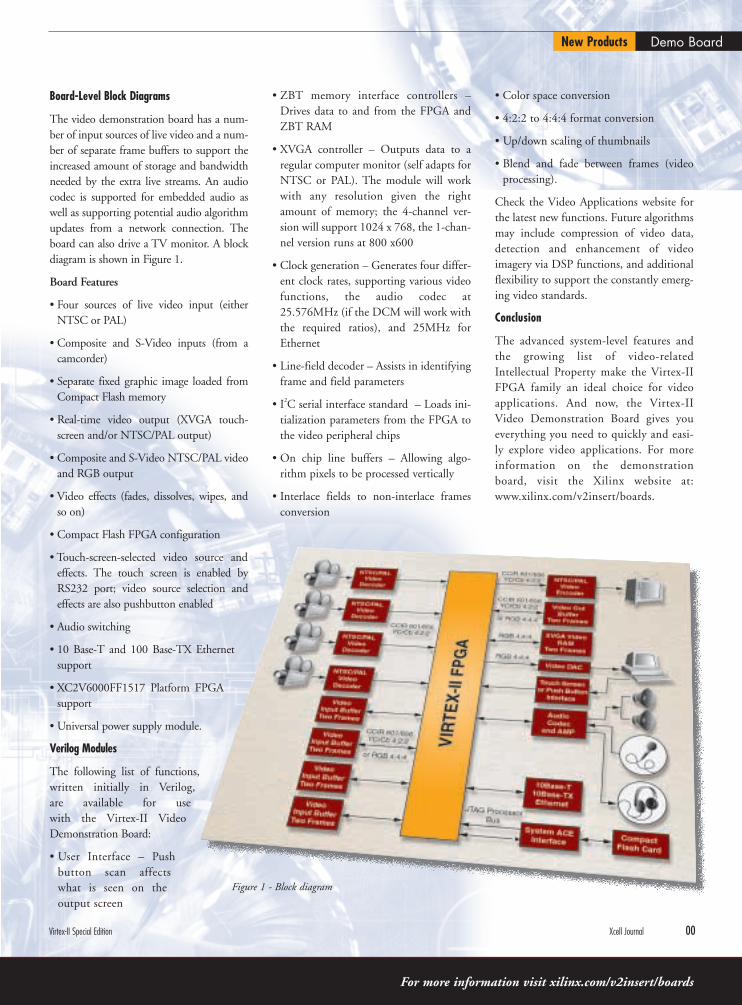
Board-Level Block Diagrams
The video demonstration board has a num-ber of input sources of live video and a num-ber of separate frame buffers to support theincreased amount of storage and bandwidthneeded by the extra live streams. An audiocodec is supported for embedded audio aswell as supporting potential audio algorithmupdates from a network connection. Theboard can also drive a TV monitor. A blockdiagram is shown in Figure 1.
Board Features
• Four sources of live video input (eitherNTSC or PAL)
• Composite and S-Video inputs (from acamcorder)
• Separate fixed graphic image loaded fromCompact Flash memory
• Real-time video output (XVGA touch-screen and/or NTSC/PAL output)
• Composite and S-Video NTSC/PAL videoand RGB output
• Video effects (fades, dissolves, wipes, andso on)
• Compact Flash FPGA configuration
• Touch-screen-selected video source andeffects. The touch screen is enabled byRS232 port; video source selection andeffects are also pushbutton enabled
• Audio switching
• 10 Base-T and 100 Base-TX Ethernetsupport
• XC2V6000FF1517 Platform FPGAsupport
• Universal power supply module.
Verilog Modules
The following list of functions,written initially in Verilog, are available for use with the Virtex-II VideoDemonstration Board:
• User Interface – Pushbutton scan affectswhat is seen on theoutput screen
• Color space conversion
• 4:2:2 to 4:4:4 format conversion
• Up/down scaling of thumbnails
• Blend and fade between frames (videoprocessing).
Check the Video Applications website forthe latest new functions. Future algorithmsmay include compression of video data,detection and enhancement of videoimagery via DSP functions, and additionalflexibility to support the constantly emerg-ing video standards.
Conclusion
The advanced system-level features andthe growing list of video-relatedIntellectual Property make the Virtex-IIFPGA family an ideal choice for videoapplications. And now, the Virtex-IIVideo Demonstration Board gives youeverything you need to quickly and easi-ly explore video applications. For moreinformation on the demonstrationboard, visit the Xilinx website at:www.xilinx.com/v2insert/boards.
• ZBT memory interface controllers –Drives data to and from the FPGA andZBT RAM
• XVGA controller – Outputs data to aregular computer monitor (self adapts forNTSC or PAL). The module will workwith any resolution given the rightamount of memory; the 4-channel ver-sion will support 1024 x 768, the 1-chan-nel version runs at 800 x600
• Clock generation – Generates four differ-ent clock rates, supporting various videofunctions, the audio codec at25.576MHz (if the DCM will work withthe required ratios), and 25MHz forEthernet
• Line-field decoder – Assists in identifyingframe and field parameters
• I2C serial interface standard – Loads ini-tialization parameters from the FPGA tothe video peripheral chips
• On chip line buffers – Allowing algo-rithm pixels to be processed vertically
• Interlace fields to non-interlace framesconversion
Figure 1 - Block diagram
Virtex-II Special Edition Xcell Journal 00
For more information visit xilinx.com/v2insert/boards
by James A. WatsonManager, Applications Engineering, Xilinx, [email protected]
Virtex®-II FPGAs are an ideal platform fordesigning with ambiguous or evolving stan-dards. Because of the inherent flexibility,reprogrammability, and extremely high per-formance (approximately 0.5 TeraMACs) ofVirtex-II devices, you can easily test differ-ent air-interface schemes and variants in-system, and you can quickly assess the sys-tem performance. In particular, Virtex-IIFPGAs make it easy to develop hybrid sys-tems such as multi-carrier CDMA orQAM-modulated OFDM.
Orthogonal Frequency Division Multiplexing (OFDM)
Currently, there are two principal 4Gdevelopment technologies contending forattention: CDMA and OFDM. CodeDivision Multiple Access is a well-knownstandard and has been used for severalyears. However, OFDM is relatively new.
OFDM, with many technical variants, isendorsed by Nokia, Cisco, Lucent, andPhilips Semiconductor, and is representedas the successor to frequency hopping anddirect sequence CDMA. It is also posi-tioned as the technique of choice for nextgeneration wireless LANs and metropoli-tan networks. The capability of OFDMto cancel multipath distortion in a spec-trally efficient manner without requiringmultiple local oscillators has won adher-ents in the IEEE 802.11a and 802.16working groups. However, despite thesupport of many key industry players,OFDM is not actually deployed in main-stream wireless systems.
Todd Carothers, vice president of market-ing for Adaptive Broadband, recently stat-ed “We’ve developed a commercialOFDM system for one application, andwe think OFDM has real advantages inthe mobile arena, but we don’t see it forfixed point. We think that adaptive timedivision multiple access is still the best
solution for fixed point-to-multipoint, andI’ll state that we still have the fastest systemout there and the most extensivelydeployed.”
Philip Gee of WiLAN said recently, “Thereis no question that OFDM and CDMA arein contention for some of the same wirelessmarkets. We believe that OFDM enjoys anumber of significant advantages, however.”
How it Works
OFDM is fundamentally different fromother modulation schemes. In fact, it shouldprobably not be considered a modulationscheme at all, because it may be transmittedvia AM, FM, QAM (Quadrature AmplitudeModulation), and so on. OFDM is proper-ly defined as a mathematically elegant tech-nique for the generation and demodulationof radio waves. Although its origins dateback to the second World War, its applica-tion to wireless communications is new.
In OFDM the subcarrier pulse shape is asquare wave. The task of pulse formingand modulation can be performed by asimple Inverse Discrete Fourier Transform(IDFT) which can be implemented veryefficiently in Virtex-II FPGAs as anInverse Fast Fourier Transform (IFFT). Todecode the transmission, a receiver needonly implement an FFT.
As you can see in Figure 1, the spectra ofthe subcarriers overlap. By using an IFFT,the spacing of the subcarriers is varied insuch a way that, at the target frequency ofthe received signal (indicated as arrows), allother signals are zero. This is known as “fre-quency orthogonality.” This contrasts withDirect Sequence CDMA, which uses aWalsh code to achieve code orthogonality.
OFDM and the Virtex-II Architecture
Virtex-II FPGAs offer several architectur-al advances that allow you to createextremely efficient implementations ofOFDM systems.
Multipliers
Virtex-II FPGAs contain a number of 18x182’s complement signed multipliers associat-ed with the block SelectRAM™ memory.
Perspective Wireless Applications
4G Wireless Systems in Virtex-IIDesigners of the 4G wireless systems infrastructure are confronted with challenging product develop-ment issues, including the uncertainty about fundamental system architectural standards such as the air interface, encryption protocols, planetary interoperability, and so on. Because there are unresolveduncertainties, you must pay close attention to risk management – making sure your designs can evolve with the changing standards.
“A must for this summer’s reading list, a real page turner...” – Dan Teie, Teie, Gelwicks & Associates
00 Xcell Journal Virtex-II Special Edition

This association allows high-speedaccess to complex multiplicand coeffi-cients, thus supporting extremely high-performance arithmetic. To see why themultipliers are so valuable, consider thenature of the FFT algorithm itself. Itessentially decomposes into a series ofmultiply-accumulate functions.
Digital Clock Management
To successfully implement OFDM, thereceiver and the transmitter must be in per-fect synchronization. Synchronizing to thetransmitter’s data clock is always necessary,whereas, carrier recovery isonly necessary in coherentdetection receivers. The dataclock must be recovered sothat the receiver will samplethe transmitted data symbolsat the appropriate time.
An algorithmic approachsuch as times-two, early-late,or zero-crossing clock recov-ery can be implemented in aVirtex-II device; all of thesefunctions are performed inthe digital domain. Thesealgorithmic approaches are perfect applica-tions for the Virtex-II Digital ClockManager (DCM). For example, the DCMsin the Virtex-II devices, along with a DDS(Direct Digital Synthesis) core, can providethe complex sinusoids necessary for demod-ulating the incoming data. Thetiming/phase of these complex sinusoids isdirected by the data recovery clock and eas-ily adjusted by the DCM’s timing controls.The DCM can also perform other func-tions vital to synchrony of the transmitterand receiver including clock deskew andfrequency synthesis.
The DCM can also de-skew the receivedsignal relative to the local receiver frequen-cy by adding digital delay. This results in asignal that is delayed but has perfect phasealignment to the local receiver frequency.
Virtex-II DCMs can drive global clockresources, general logic interconnect, andI/O pads simultaneously. This providesmaximal flexibility when placing logic.
tops of buildings, and so on, and manuallyupgrade circuit boards in the base stations.Keep in mind that many of these base sta-tions are deployed in regions of the worldthat suffer climactic extremes. This expen-sive and potentially dangerous upgradepath is part of the cost of ownership of abase station constructed around conven-tional ASICs.
Now consider a base station constructedwith a Virtex-II Platform FPGA; the con-figuration of the cellular base station maybe completely altered simply by transmit-ting a new Virtex-II configuration file from
the comfort of a centraloffice. This technique isextensible, so that an entirenetwork can be reconfigured,automatically, without replac-ing any hardware. This capa-bility allows you to more rap-idly introduce the product tothe market and helps to pro-tect the base station architec-ture against obsolescence.
There is another degree of flex-ibility which the Virtex-II-based OFDM base station pro-
vides, the ability to trade off silicon area forperformance. Consider the market successfactors described above. If it became evidentthrough field trials and customer testing thatthe average customer was not a heavy con-sumer of bandwidth, the OFDM algorithmcould be re-targeted to use more general pur-pose logic. Properly done, this would resultin the ability to support more channels in thesame device. Essentially, the Virtex-IIPlatform FPGA allows you to dynamicallytrade off silicon area for performance.
Conclusion
The Virtex-II product family is uniquelysuited to the demanding digital signal pro-cessing that will be required to roll out next-generation broadband wireless services. Itspowerful suite of dedicated high-perform-ance logic functions such as the high-speedmultipliers and DCM, along withextremely versatile high-performance gen-eral logic, define an optimal solution forwireless designs.
High Performance
The most valuable feature of the Virtex-IIfamily, for implementation of advancedwireless systems, is the extremely high-per-formance. This gives you a great degree offreedom that is not available with alterna-tive implementations, such as ASICs. Tounderstand the value of this advantage,consider the following scenario.
OFDM Field Deployment Example
In this example, an OFDM system isdeployed on an experimental basis by awireless service provider. It is located in an
urban market, but there are many businessfactors that must be addressed if the ven-ture is to succeed, including:
• Which of the emerging broadband wire-less services will generate high demand?
• What is the peak bandwidth per subscriber?
• What is the average bandwidth per sub-scriber per service?
• What Quality of Service factors can beused to differentiate the new service?
There is no substitute for field trials toanswer these questions, and there is nobetter platform for field trials thanVirtex-II FPGAs.
Consider a case where a standards bodyadopts a new variant of OFDM, a verylikely scenario. With conventional ASICs,the upgrade path is painful. Utility workersmust climb telephone poles, climb to the
Users
Frequency
1 2 3 4 5 6
AmplitudeAllocated Bandwidth
Figure 1 - OFDM allows for greater spectral efficiency
Virtex-II Special Edition Xcell Journal 00
For more information visit xilinx.com/v2insert/wireless
Perspective Wireless Applications
CLB
Reso
urce
s BL
K RA
MCL
K Re
sour
ces
I/O F
eatu
res
Spee
d
System Gates
CLB Array (Row X Col)
Number of Slices
Logic Cells
CLB Flip-Flops
Max.Distributed RAM Bits
# Block RAM Blocks
Block RAM Bits
# Dedicated Multipliers
Digital Clock Manager(Frequency min/max)
# DCM’s
Frequency Synthesis
Phase Shift
Digitally Controlled Impedance
Number of Differential I/O Pairs
Max.I/O
I/O Standards
Commercial Speed Grades(slowest to fastest)
Industrial Speed Grades(slowest to fastest)
Serial PROM Family
Config.Memory (Bits)
VIR
TE
X-I
I
Virt
ex-II
Fam
ily —
1.5
Vol
tXC
2V40
40K
8 x
825
657
651
28K
472
K4
1/42
04
YES
YES
YES
4488
XC2V
8080
K16
x8
512
1,15
21,
024
16K
814
4K8
1/42
04
YES
YES
YES
6012
0XC
2V25
025
0K24
x16
1,53
63,
456
3,07
248
K24
432K
241/
420
8YE
SYE
SYE
S10
020
0XC
2V50
050
0K32
x 2
43,
072
6,91
26,
144
96K
3257
6K32
1/42
08
YES
YES
YES
132
264
XC2V
1000
1M40
x 3
25,
120
11,5
2010
,240
160K
4072
0K40
1/42
08
YES
YES
YES
216
432
XC2V
1500
1.5M
48 x
40
7,68
017
,280
15,3
6024
0K48
864K
481/
420
8YE
SYE
SYE
S26
452
8XC
2V20
002M
56 x
48
10,7
5224
,192
21,5
0433
6K56
1008
K56
1/42
08
YES
YES
YES
312
624
XC2V
3000
3M64
x 5
614
,336
32,2
5628
,672
448K
9617
28K
961/
420
12YE
SYE
SYE
S36
072
0XC
2V40
004M
80 x
72
23,0
4051
,840
46,0
8072
0K12
021
60K
120
1/42
012
YES
YES
YES
456
912
XC2V
6000
6M96
x 8
833
,792
76,0
3267
,584
1056
K14
425
92K
144
1/42
012
YES
YES
YES
552
1104
XC2V
8000
8M11
2 x
104
46,5
9210
4,83
293
,184
1456
K16
830
24K
168
1/42
012
YES
YES
YES
554
1108
LDT-
25,L
VPEC
L-33
,LV
DS-3
3,LV
DS-2
5,LV
DSEX
T-33
,LVD
SEXT
-25,
BLVD
S-25
,ULV
DS-2
5,LV
TTL,
LVCM
OS3
3,LV
CMO
S25,
LVCM
OS1
8,LV
CMO
S15,
PCI3
3,PC
I66,
PCI-X
,GTL
,GTL
+,H
STL
I,HS
TL II
,HST
L III
,HST
L IV
,SS
TL21
,SST
L211
,SS
TL3
I,SS
TL3
II
-4 -5
-6-4
-5-4
-5 -6
-4 -5
-4 -5
-6-4
-5-4
-5 -6
-4 -5
-4 -5
-6-4
-5-4
-5 -6
-4 -5
-4 -5
-6-4
-5-4
-5 -6
-4 -5
-4 -5
-6-4
-5-4
-5 -6
-4 -5
-4 -5
-4
ISP
OTP
.15u
m E
ight
Lay
er M
etal
Pro
cess 0.4M
0.6M
1.7M
2.8M
4.1M
5.7M
7.5M
10.5
M15
.7M
21.9
M29
.1M
Virt
ex-II
pac
kage
s FG
456
and
FG67
6 ar
e fo
otpr
int c
ompa
tible
.Vi
rtex
-II p
acka
ges
FF89
6 an
d FF
1152
are
foot
prin
t com
patib
le.
Impo
rtan
t:Ve
rify
all
Dat
a w
ith
Dev
ice
Dat
a Sh
eet
Num
bers
indi
cate
d in
the
mat
rix a
re th
e m
axim
um n
umbe
r of u
ser
I/O’s
for t
hat p
acka
ge a
nd d
evic
e co
mbi
natio
n.
XC2V40
XC2V80
XC2V250
XC2V500
XC2V1000
XC2V1500
XC2V2000
XC2V3000
XC2V4000
XC2V6000
XC2V8000
Pins
Body
Siz
e88
120
200
264
432
528
624
720
912
1104
1296
Chip
Sca
le P
acka
ges
— w
ire-
bond
chi
p-sc
ale
BGA
(0.8
mm
bal
l spa
cing
)
144
12 x
12
mm
8892
92
BGA
Pac
kage
s (B
G) —
wir
e-bo
nd s
tand
ard
BGA
(1.2
7 m
m b
all s
paci
ng)
575
31 x
31
mm
328
392
408
728
35 x
35
mm
456
516
FGA
Pac
kage
s (F
G) —
wir
e-bo
nd f
ine-
pitc
h BG
A (1
.0 m
m b
all s
paci
ng)
256
17 x
17
mm
8812
017
217
217
2
456
23 x
23
mm
200
264
324
676
27 x
27
mm
392
456
484
FFA
Pac
kage
s (F
F) —
flip
-chi
p fin
e-pi
tch
BGA
(1.0
mm
bal
l spa
cing
)
896
31 x
31
mm
432
528
624
1152
35 x
35
mm
720
824
824
824
1517
40 x
40
mm
912
1104
1108
BFA
Pac
kage
s (B
F) —
flip
-chi
p fin
e-pi
tch
BGA
(1.2
7 m
m b
all s
paci
ng)
957
40 x
40
mm
624
684
684
684
684
Virt
ex-II
(1.5
V)
I/O’s
PAC
KA
GE O
PTI
ON
S A
ND
USER
I/O
PR
OD
UC
T SELE
CTI
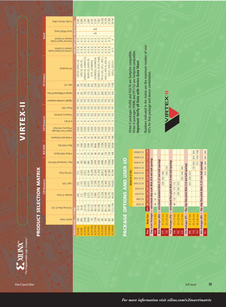
ON
MA
TRIX
Virtex-II Special Edition Xcell Journal 00
For more information visit xilinx.com/v2insert/matrix
THE PLATFORM FOR POWERFUL SOLUTIONS.
THE FIRST PLATFORM FPGAIt’s here. The next generation of the most remarkable programmable
logic device ever introduced: the Virtex-II FPGA.
The first embodiment of the Platform FPGA, the Virtex-II solu-
tion is the ultimate system design platform, delivering SystemIO™
interfaces to bridge emerging standards and address all aspects of
system connectivity. For the first time in the industry, designers facing
the challenges of signal integrity, system timing, EMI issues and
design security have a programmable platform that heralds a new era
in high-performance designs.
The world’s first Digitally Controlled Impedance
Technology (XCITE™) dramatically simplifies board design and
maximizes system performance. IP Immersion™ architecture enables
easy integration of hard and soft IP. XtremeDSP delivers over 600
billion MACs/s of processing power. Unique Digital Clock Managers
allow unparalleled levels of flexibility in high-speed customized
clock design.
Watch for more on the Platform FPGA . . . it’s where the system
design world is going.
The Programmable Logic CompanySM
www.xilinx.comFor more information visit xilinx.com/v2insert/solutionsadPN 0010617