Embed Size (px)
Citation preview

AFCRL-71-0500 013630-8-T
TTHE UNIVERSITY OF MICHIGANCCOLLEGE OF ENGINEERING
DEPARTMENT OF ELECTRICAL ENGINEERING
Radiation Laboratory
Techniques for Broadband Control ofRadar Cross Sections
ByVALDIS V. LIEPA and E. LAWRENCE McMAHON
September 1971
Scientific Report No. 11 f2V n7,r2Contract No. F19628-68-C-0071Project No. 5635Task No. 563502Work Unit No. 56350201
Approved for public release; distribution unlimited.
Contract M~nitor: JOHN K. SCHINDLERMICROWAVE PHYSICS LABORATORY
Prepared for:Air Force Cambridge Research LaboratoriesAir Force Systems CommandLaurence G. Hanscom Field by
Bedford, Massachusetts 01730 NATIONAL TECHNICALINFORMATION SERVICE
X p-,jold. VA 22151
Administered through:
OFFICE OF RESEARCH ADMINISTRATION ANN ARBOR

.-UNCLASSIFIED............
VOCUME-NT CONTROL DATA -R & D. p1', , # le, 'lw)* of' Uf Ih t i I Ol le I Ing ridn ftline e t onfelll a,, O ur 6 # */#I f', a "I, fs tHer 0 v it It ,,fI I , .i Ii's "C fi 'I/
IThe University of Michigans Radiation Laboratory UNCLASSIFIED'Department of Electrical and Computer Engineering ab, .OUP2455 Haward Street, Ann Arbor, Michigan 48105 ......
TECHNIQUES FOR BROADBAND CONTROL OF RADAR CROSS SECTIONS
Scientific Interim., I -4O0 N 1 I t nme., meddle inileal, lasI hine)
Valdis V. Liepa.E. Lawrence McMahon
I.,
e p.. To.L ?8, TOtAL NO. 00' JaE NO OP NftS
LSeptember 1971 49 2L!bt., N% T MAC T 00 GN ANT NO. 90. ORIGINATOR'S RIqPORI NUM69ISI4
F19628-68-C-0071 013630-8-T
Project, Task, Work Unit Nos. Scientific Report No. 11 4
; 5635-02-01 96. oTHER A PORT NO5e (Any ohe, umbrs diat MAY b 10.1440(IDoD Element 61102F t,, ,el,)
DoD Subelement 681305 AFCRL- 71-0500oivrsTi.1or STATEcmcNT
A .- Approved for public release; distribution unlimited.
r..C..1 %O An $a.C SPONSORING MILITARY ACTiVITY
Air Force Cambridge Research Laboratories (LZ)TECH, OTHER L. G. Hanscom Field
_ _._ _ _ _ Bedford, Massachusetts 01730
* -Methods of realizing the load impedance required for radar cross section controlof conducting bodies are discussed. It is shown that passive loading, using frequency-dependent dielectric/magnotio materials in a radial or coaxial line, requires a frequency
* dependence which is not exhibited by any known material.
" A number of active synthesis approaches.are examined, with emphasis on those.using the Negative Impedance Converter (NIC). Experimental results are given for a
particular NIC realization operating in the 5 - 10 MHz range; the circuit is shown to becapable of producing the load impedance required for a cross-section reduction of 13dB
* nr more over a 2:1 bandwidth. /
I
D D I .V o, 14 7 3 UNCLASSIFIEDSecunty clhssi 1¢ ln13

I UNCLASSIFIED
xcv' WORDS f41Pd -~w
OFT M OLw WT MOL
Impedance LoaxinActive SynthesisNegative Impedance ConverterBroadbandReduction of Back Scattering
* Radar Cross Section Control
gII
I Iij
* I•- it
II
~UNCLASSIFID
IOOM 0I2C&

L
AFCRL-71-0500 013630-8-T
Techniques for Broadband Control of Radar Gross Sections
By
Valdis V. Liepa and E. Lawrence McMahonThe University of Michigan
Radiation Laboratory2455 Hayward %reet
Ann Arbor, Michigan 48105
September 1971
Scientific Report No. 11Contract F19628-68-C-0071Project No. 5635Task No. 563502Work Unit No. 56350201
Approved for public release; distribution uilimited.
Contract Monitor: John K. SchindlerMicrowave Physics Laboratory
Prepared For
Air Force Cambridge Research LaboratoriesAir Force Systems CommandLaurence G. Hanscom Field
Bedford, Massachusetts 01730
I

. . . . . - . ..-
013630-8-T
ABSTRACT
Methods of realizing the load impedance required for radar cross
section control of conducting bodies are discussed. It is shown that
passive loading, using frequency-dependent dielectric/magnetic materials
in a radial or coaxial line, requires a frequency dependence which is not
exhibited by any known material-
A number of active synthesis approaches are examined, with emphasis
on those using the Negative Impedance Converter (NIC). Experimental
results are given for a particular NIC realization operating in the 5 - 10MHZ
range; the circuit is shown to be capable of producing the load impedance
required for a cross-section reduction of 13dB or more over a 2:1 bandwidth.
ii

- 013630-8-T
It
ITABLE OF CONTENTS
ABST1ACT I
ACKNOWLEDGEMENTS iv
I INTRODUCTION
U BACKGROUND 3
HI USE OF FREQUENCY-DEPENDENT MATERIALS 12-_ 3.1 Loading of a Radial Cavity 12
k 3.2 Loading of a TEM Transmission Line 15
IV CENTER LOADING 244.1 Introduction 244.2 Reflection Coefficient Realization 254.3 Impunce Realization 264.4 The Negative Impedance Converter 274.5 NIC Theory 274.6 NIC Circuits 334.7 The Yanagisawa MIC 36
V EXPERIMENTAL RESULTS 395.1 Measurement Techniques 39
VI PROSPECTS FOR FURTHER DEVELOPMENT 46
REFERENCES 48
I
r=-
I,L: t

013530-8-T
ACKNOW-LEDGEMENTS
The authors wish to express their gratitude io Prof. T. B.A. Senior,
who directed and coordinated the work described in this report, and who
also contributed a great deal through discussions, comments, etc. Our
specia! thanks are due to Mr. Charles B- Loftis, who performed most of
the tedious experimental work and imany of the calculations; his contribu-
tions tc the experimental work were invaluable.
iv

013630-8-T
INTRODUCTION
Impedance (or reactive) loading is a potential!y powerf.il method for
modifying scattering behavior and- in particular, for reducing the back scatter-
ing cross section of an object-Theoret:caly at least, it is possible to modify the scattering in almost
any desired marner providing the loading configuration has the required sophisti-
cation; in partimular, zero back scattering is feasible. Not surprisingly, the
exact loading necessary to achieve this depands oa the shape and size of the target.
the location of the load and, in general, the direction of the in-idence. It is also
a critical function of frequ--ncy, which is the principal drawback, but in spte of
thi4 the method has been shown to work over a few per cent bandwidth for a variety
of simple target shapes including spheres. cylinders (thick and thin), and spheroids.
In essence, the technique is to introduce an impedance over a restricted
portion of the surface using a cavity-backed slot, lumped network or other type
of microwaxe circuit, and as such it is only a special case of the general theory
of surface impedance effets. Mathematically at east, it is similar to the appli-
cation of absorbers, but in practice differs both in the localized nature of the
region where the loading is emy-;qed and in the greater variety of impedances
that can be achieved either to enhance or decrease the scattered field. Alteraa-
tively, one could seek to generate the loading by attaching dipoles or other s-tub
antennas to the surface of the target, and this technique has also received some
atentior. In either ca!e. the precent limitations of the loading method remain
the same, namely, sensitivity to frequency and aspect.
Whether the loading to provide the desired radar cross section cont-ol is
provided by cutting slots in the scurfae or by attaching external scatterers, the
frenuency behavior of the impedances associated with thes loading devices is

a.- -2Lif W111rn. S -. - --
....... ------ = - = = ,a E. - - - --"
- - -
0 13630-8-T
(at least qualitatively) independent of the shape of the body and the position of the
load, and is the opposite of that provided by a series RLC network or shorted
transmission line. Consequently, when such means are used to simulate the desired
loading, the exact impedance can be provided only at a single frequency, which
then leads to a narrow-band performance.
Over the last few years the Radiation Laboratory has sought ways of
increasing the bandwidth of the impedance loading technique with particular
reference to the frequency range 59-100 MHz. Both active and passive methods
of realizing the required loads have been studied and we here present some of the
res-aits obtained. Section I summarizes some of our earlier theoretical and
exoerimtntal work on the loading method and. in particular, shows the type of loading
variation with frenuencv necessary to suppress back scattering cross sections in
the resonance region. The possibility of achieving this variation by inserting a
frequency-dependent material into a radial cavity or coaxial line is examined in
Section H. The required frequency behaviors of the relative permittivity and
permeability are compared with those attainable using existing materials.
Althowgh the results provide no basis for optimism at the moment, some
of the active network synthesis approaches for achieving the desired loading appear
more promising. In Section IV various types of circuit are examined, with empha-
sis on the Negative Impedance Converter (MC). An active load using a particular
NIC circuit was constructed for use in the 5-10 MHz range and measured values
of its performance have showlin it capable of producing the loading required for at
least a !3 dB cross section reduction over a 2:1 bandiwidth. The advances in high
perfor mance transistors and in circuit techniques necessary to duplicate this
achievement at a ten-fold larger frequency are discussed in Section VI.
2

013630-8-T
- II
BACKGROUND
The idea of using loading to reduce the reradiated fields dates back to
the L920's (Meissner, 1929). when it was t-ommon practice to use lumped induc-
tors and capacitors to det.ine the supporting structures for broadcast transmitting
antennas whenever their lengths were near resonance and interfered with the
antenna radiation patterns. The first reported application of the loading technique
for scattering reduction at microwave frequencies was by lams (1950), who used
a coaxial loading to decrease the scattering from metallic posts in a parallel-plate
pillbox structure. King (1956) investigated the change in current distribution on a
thin cylindrical rod when a central load is introduced, and later Hu (1958) and Xs
i- and Schmitt (1958) showed that a high reactive Impedance can appreciably affect
the scattering behavior of such a rod.
Nevertheless, the potential of this technique as a means of cross section
reduction in the resonance region was not appreciated until the early 1960's.
Following a study at AFCRL. Sletten (1962) reported that for cylinders approxi-
mately X/2 in length, and X/4 and X18 in diameter, significant reductions in
their broadside cross sections could be obtained by reactive loading at their cen-
ters, and shortly after, work was commenced at the Radiation Laboratory aimed
at exploring the use of reactive (impedance) loading as a means of reducing the
cross sections of thin and thick cylinders, spheres and spheroids.
in view of Sletten's work, the loading of a circular cylinder was studied
first (Chen and Liepa. 1964). A thin circular cylinder of length t, 0 < I < 2X,
was chosen si-ce adequate mathematical tools were already available (King, 1956)
for an analysis of the scattering. An approximate solution of the integral equation
for the current on the cylinder was obtained as a function of the central load, ZL ,
and from this an expression for the far field was derived and computed. It was
found ihat the back scattering cross section at broadside could be rediced tu. zero
by appropriate choice of load, and that a non--:ero resistive component, RL, was
3

901K30-8-T
in general necessary for this purpose. It was further shown that for a cylinder
of length I < X this optimum loading was passive (R > 0), whereas for a cylin-0 Lder of length X < 2X and active (RL < 0) load was usually required. The cor-
responding reactive component XLs in general, had a negative slope (XL/aW< 0).
For cylinder lengths near resonance ( e- X/2) or shorter, a loading which de-
creases the back scattering at broad'3ide also decreases the magnitude of the cur-
rent induced in the yjlinder by as much as 70 per cent, and, in consequence, this
same loading reduces the bistatic scattering at all aspects other than end-on, as
well as back scattering for oblique incidence. For a cylinder beyond resonance,
however, the loading to reduce the back scattering cross section at broadside is
not so effective for bistatic angles or for oblique incidence. The reason for this
becomes clear when the dipole currents are examined for the case of oblique inci-
dence. By dividing the current into components which are symmetric or anti-
symmetric with respect to the center of the cylinder, it is obvious that a center
load affects only the symmetric component and leaves the anti-symmetric one
unaltered, suggesting that double loading would be desirable for this application.
A theoretical investigation of a thin cylinder with two equal loads symmetricelily
placed was carried out by Chen (1965), who showed that loading positions could be
found at which the impedances necessary to suppress the contributions to the back
scattered field provided by both the symmetric and anti-symmetric modes were
approximately thL same. Under the stipulation of passive loading (.T > 0), he
found that the back scattering cross section could be significantly reduced at almost
all angles of incidence for cylinders up to 1. 5X long. This suggests that if imped-
ance loading is used to reduce the return from large bodies at all aspects, the leads
should be placed not more than 0. 75X apart.
The impedance loading of a sphere was investigated next. The main reasons
,or choosing such a shape were the desire for a body having a carrying capacity,
and one for which analyses could be carried out which are effectively exact regard-
less of frequency. Some of the uncertainties present in the analysis of even a thin
cylinder of length greater than 2A could now be avoided.
t4
FN-11

013630-8-T
The particular case studied was that of a metallic sphere loaded with a
slot in a plane perpendicular to the direction of incidence (Liepa and Senior,
1964, 1966). The slot was assumed to be of small but finite width with a constan
electric field across it; under this assumption the analysis for the external fields
was exact. Expressions for the scattered far field components as well as the total
surface field components were derived, and these were used to investigate the
modifications to the scattering cross section produced by various slot admittances.
The numerical work was limited to the range 0 < ka < 10, where k is the propaga-
tion constant of free space and a is the radius of the sphere.
It was foundthat the loading admittance necessary for any given modification
is in general complex, with positive or negative real part corresponding to energy
absorbing or radiating loads respectively. The loading required to reduce the
back scattering cross section to zero was examined in some detail. It was shown
that for any given slot position, the ranges of ka in which the real part of the load-
ing admittance is negative or positive alternate with one another, with the locations
of these bands being functions of the slot position. For example, with the slot at
the shadow boundary (60 = 90°), there are three negative bands in the range0 < ka < 10, but as the slot is moved towards the front of the sphere, these bands
appear to slide in the direction of increasing ka.
At selected frequencies for which the demanded loading is reactive, the
theoretical predictions were confirmed by measurements made using a sphere with
a circumferential slot backed by a radial cavity whose depth could be varied by
inserting discs of the appropriate diameter. Back scatter reductions in excess of
20 dB were observed, and measurements of both the surface and back scattered
far fields as functions of angle for various reactive loads were performed to verify
the theory.
Unfortunately, the variation of susceptance with frequency fot the radial
cavity (or any other 3less network) is the direct opposite of that required to
5

013630-8-T
reduce (or enhance) the back scattering cross section. As a result, the loading
can be satisfied only where the two admittance curver intersect, and narrow band-
widths are therefore to be expected. To determine the actual bandwidths encoun-
tered with susceptive loading, the case when the sphere is loaded at the shadow
boundary (80 = 900) for zero back scattering was examined at ka = 4. 28. The
required optimum loading and that supplied by a radial cavity (such as used in the
experimental model) are shown in Fig. 2-1a. The depth of the cavity was chosen
to prouuce this optimum loading at ka = 4.28. it is evident that the corresponding
curves, especially for the real part, have completely different behaviors, and a
minute deviation in frequency from the critical value therefore results in a large
difference between the desired and the supplied loadings. The cross section cor-
responding to the cavity loading is shown in Fig. 2-1o. As expected, complete
suppression is achieved at ka = 4.28, but the reduction is highly frequency
sensitive. For example, for a 10dB reduction in the cross section, the bandwidth
is 6.5 per cent and decreases to only 2 per cent when a 20 dB reduction in the
cross section is desired.
It is obvious that the chances of achieving broadband loading are greatest
in the frequency range where the variations of the required admittance are smallest.
Fortunately, such a frequency range corresponds to the so-called resonant region
where the back scatiering cross section exhibits pronounced oscillations as a function
of frequency. For example, with a slot of angular width 0.0332 radians and located
at 00 = 600, i.e. 300 forward of the shadow boundary, the real and imaginary
parts of the normalized loading admittance that must be provided at the slot to pro-
duce zero back scattering are shown as functions of ka in Fig. 2-2. It is at once
apparent that the variation of the susceptance as a function of frequency (or ka)
has primarily a negative slope and is, in fact, almost the reverse of that provided
by a typical cavity. It is therefore not surprising that when one attempts to gen-
erate the required loading using elementary devicep, radar cross section reductions
can be achieved over a bandwidth of a few percent at most.
6
Ek

k44
4J g
0 I.
C0 2
ID 4.4
4t4
CC400
-o 0 07
..s........

01363-8-T
- 20
10
Y, /Y 0 0.0.5 1.0 ka 1 *
-10
-20
FIG. 2-2: Real -)and imaginaxy (--)parts of the optimumloading admittance for zero back scattering with 86 60o
8

El0 363'0-8-T
SThe orientation of the sphere loading considered by Liepa and Senior
(1964, 1966) is ana'_ytically convenient since only the tesseral harmonics of the
first order appear in the expressions for the surface and far fields. Practically,
however, the choice is not so desirable. The fact that the voltage appearing
across the slot has an asymmetric (cos 0) distribution means that the loading must
be distributed around the slot and cannot be lumped as a single load at the center
of the cavity where the voltage is zero. In order to reduce the complexity of the
practical loading problem, the treatment of Liepa and Senior was now extended to
E the case of an azimuthally-loaded sphere at arbitrary incidence (Chang and Senior,
1957). The analysis paralleled in large measure that previously given, the only
major difference being the occurrence of doubly-infinite sets of modes. Analytical
expressions for the surface and far field components were presented, as well as
ii' for the loading necessary to produce selected forms of cross section control. Once
again emphasis was placed on the reduction of the back scattering cross section,
and in general there is n~w the choice of loading each mode so as to suppress its
individual contribution, or of loading one mode (taking into account the effect, if
any, of that load on all other modes) so as to suppress the net contribution in the
far field. Practically, however, the former type of load would be almost impossible
to realize, and since a load placed at the center of a radial cavity affects only the
zero order mode, it is most convenient to load in this manner whenever the zero
order mode is present, i.e. for all angles of incidence other than normal to the slot.
In both the numerical and experimental work, attention was concentrated
on the case of a circumferentially-loaded sphere with the slot in the plane of inci-
dence and normal to the incident electric vector. In the lower resonance region at
least, the zero order mode is then the dominant contributor to the far field back
scattering of the unloaded sphere, and adequate cross section control can be achieved
using a single lumped load at the center of a radial cavity. The real and imaginary
Fi parts of the impedance at the center necessary to give zero back scatter were com-
pated as functions of ka, and in Fig. 2-3 the curves are reproduced for the case of a
R
9

013630-8-T
6
4 -0.2
2 0.1
I.Fz]1 0 R Ii
-6o0J .5 \\ 1.o0. 1.5 L
-2 -\ \
FIG. 2-3: Real (-) and imaginary (-...) parts of the optimum loadingimpedance at the center of a sphere for zero back scat.'ering.
10
I

013630-8-T
slot of width 0.0399 radian. Again the reactive part of the demanded load
exhibits the negative slope common to all the cases considered.
Closely related to the problem of narrow bandwidth is the extremely tight
tolerance on the loading which is presented if the desired reductions in the radar
cross section are to be obtained. McMahon (1969) computed the back &cattering
froin a sphere with various loading impedances, and by plotting cross section con-
toni s for each frequency (or ka) on the impedance plane, he found that to produce
a reduction in the back scattering cross section of at least i13dB. the real and
imaginary parts of the load must be within + 0. ! IZ of their optimum values (Fig. 2-3).
It follows that whatever means are used to produce the loading, very tight control
must be exercised over the circuit components and/or loading materials.
Another approach to the loading problem that should be mentioned here is
the compensation method in which the scattering of a body is modified by attaching
external scatterers which are in turn loaded by impedances. The advantage of !sach
a method is that the loading of the body is accomplished externally and thus the
parent body does not have to be modified by cutting slots in the surface as in the
cases discussed above. Chen (1966: used the compensation method to minimize the
back scattering of a conducting cyindea- by staching a ain loaded wire near to the
surface. Later, Chen and Vincent 1368) us,-d the same technique to modify the
radar cross section of a metallic sphere by attaching two thin, loaded moropoles
on the opposite side of the sphere. In both cases it was found that the impedance
required to annul the back scailering cross section is qualitatively the same as that
for a slot cut into the surface of the b"y; in particular, the sl--pe of its reactive
part is still negative.
ii
E

USE OF FREQUENCY-DEPEN.\DENT MNATERLA-LS
A possible (though not necessarily realizable) method to achieve the
desired loading over a significant frequency band is to consider a cavity filled
with a homo-geneous isotropic material of complex- permeability and Wermittivity,
and tOwn allow these constants to -vary as a function of ireoatencv in order to obtain
the desired impedance- Tw.o cases have been studied: (a) the loading of a radial
cavity and Wb the loading of a TEM transmission line-. The results are presented
in this Section.
3- i Loading of a Radial Cavity
The original boundary value problem for this case w-as studied by Liea ad
Senior (49166) and ended by specifying the real and imaginary parts of the loading
admittance required to annul the back scattering croscs seclion of the sphere. Con-
sider the case of a sL at 0 60 (i. e- 300 forwr of th shadow oudryo
angular width 0. 0392 radian. The real and imaginary parts of the normalized load-
ing admittance Y,/JY tha--t must be p)rovided for zero back scattering are shown as
functions of ka in Fig. 2-2. A method of generating the required admittance isto
bac'k the slot wit-h a radial cavrity. Liepa and Senior did this in their experimental
study, but. due to the incompatabilitv of the admittance demanded and that suolied
by the radial cavity, the demanded loading could be supplied only at spot frequencies.
It is this inc-3mpatabiiitv that results in the narrow band perform ance of the loaded
sphere (cf. Fig. 2-.. for example) and of the impedance loading technique ingnrl
If the radial carviv is loaded with a mn-aterial whose electric pnroperties vary
wit frequency, wna-t would be2 the demandsz on th- treqiisncy xvariation? Toanse
this que~stion, a study was performed (Senior and Knott- i967a, b) of a radial cavity
barnng the Slot and filied with P- homogenc-ous isotropic material of comblex (relative)
permitiht C - and permeabilityL.- T-he input idriittance. relative to free space.
of su!ch cavil% i given by
12

003630-8-T
k 1 k a) N (k kb) -N(k k2)J(k -kb)yly -2 ~ Ir Irr ar
r ±r r r ±r
where d is the width of the cavity. b is the radius of the inner short, and
kr= \TW .(3.2)
The values of the parameters a and d are fixed by the model and henceforth we
V shall take
a/d =25- 064 (3.3)
corresponding to a slot of angular width 0. 0392 radian. The parameter b can be
varied, but once a v-alue has been chosen, it is assumed that it cannot be changed
to Produce any impedance variation.
Using a combined analytical--graphical approach, Senior and Knott compuited
values for pu and C which. when inserted in Eq. (3.!)- -would generate the opti-
mum loading admittance value given in Fig. 2-2-. The compuztation was a rather
involved and lengthy one and we shall therefore present only the resdts. Fig.. 3-1
shows the real and imaginary parts of the relative permittivity C and relativer
permeability p necessary to achieve the desired loading. The condition M p IE
is not essential. but does limit the data to one pair of curves; it also maximizes
the minimum loss tangent over the range. and minimizes the total variations of the
real parts of M and E - In general it is seen that the real Dart of the requiredr r
c is a decreasing function of frequency varying from about 4. 6 to !.4 over
the frequency range considered, and the corresponding imaginary part has an inverted
bell-shane behavior -with an average value ofl about 0. 06.
In searching for suchn. material, ;various books, reports. etc. -have been
consulted and the Problem has been discussed with a fe-rrite manufac turing group.
bu unfortunately no material has been found which exhibits the Jfrequenc:* behavi r
appropriate to the optimum- loading.. Some ferrite materials do exhibit a frequency
13

- 1 1- S --01
4 -0.08
7 K yiqycr]-
2 R-0.04-Er
0 00.51.15
Normalized Freqincy
FIG.3- I :Beai andi imaginry mxts of F,. E neeary to achieve the
rezjuired impedance in a radial cavity when ur =Zr

0 13630-8-T
variation whose real parts resemble that demanded, but they also possess imaginary
parts of the same order of magnitude as the real parts. As such, tie imaginary
:7 parts are about two orders of magnitude larger than those required for optimum
loading (see. for example, Smit and Wijn. 1959).
What cross section reduction can be expected if we place in the cavity a
material whose real part matches that demanded, but whose imaginary part is
greater by two orders of magnitude? This particular aspect of the problem has
not been studied directly. but judging from the negative results of a related exper-
imental study (Senior and Knott. 1967a) in which a cylindrical structure was loaded
with iossy dielectric material to reduce its cross section over an extended fre-
quency range. as well as the study of loading impedance tolerances for a sphere
(McMahon, 1969), one could expect at most a few dB reduction in cross & Zrion.
R9 In fact, depending on the frequency. an enhancement in cross section could occur.
W3.2 Loading of a TEM Transmission Line
In this Section we examine how the electrical properties of materials placed
in a transmission line (coaxial cavity) of fixed length must vary with frequency to
produce at the line input the desired impedance over a significant frequency range.
Specifically, the impedance desired is that required for zero back scattering in the
case of a sphere loaded at the equator with a circum'rential slot perpendicular to
the incident electric field vector. The slot is backed by a radial cavit- which, in
tuf--, is terminated at the center by an impedance Z0- This is then the impecznce01that must be realized if a cross section reduction over a given frequency range is
to be achieved.
To ;implify the formulation, as well as the computation, assume that the
impedance Z is generated by a coa.xial cavity uniformly filled with a homogeneous
isotrrpic material whose electric properties are to bee de.ermined tc produce Z C.
The expression for the input impedance of a segment of a transmission line is well
known, but is usually given for the case when the transmission line is lossless
15

013630-8-T
(cf. Ramo and Whinnery, 1958). However, the same formula can also be used
when the line is filled with a lossy material by allowing the permittivity and per-
meability to take on omplex values. In this case, the input impedance is given by
Z. =Z Z IZcos (krl) + jZrZ 0 sin (kr Id)Zin =ZrZ0 ZrZ0 cos(krld) -jZe sin(krke) ' (3.4)
where
Zr = Prr : relative characteristic impedance of the line,Zr r
Z= characteristic impedance of the line when unloaded,
Z = terminating impedance for the line,
k = , : relative propagation constant,r rr'AKI
k = free space propagation constant,
and I = length of the line.
Both M r and Er are complex, and because they are contained in the sine and cosine
functions as well as the expression for Z , it would be very difficult (even in specialr
cases) to solve for M r and E. explicitly. To determine the optimum M r and 4
corresponding to the required input impedance, an error function E was defined as
E= z0 -ZinI , (3.5)
where Z. is given by Eq. (3.4), and Z is the impedance that must be generated
by the loaded line at each of several specified frequencies. The computation of the
optimum impedance Z for zero back scattering was carried out by Chang and
Senior (1967) and the results are presented in Fig, 2-3. They are also repeated
in Table 3. 1 where the values are given to 4 significant figures. Note that even
though the loading in this case "s at the center, and the problem is different from
that considered in Section 3. 1 in that the slot is normal to the incident electric field
16
L

t013630-8-T
vector instead of normal to the direction of incidence, the general character of
the optimum impedance is still the same-the imaginary or reactive part has a
negative slope and the real part is sniall and positive.
TABLE 3.1
Optimum Impedance for Zero Back Scattering
Ia Re[ZJe Im[ZOf
0.5 .7860 x 10 5.798
0.6 .1705 x 10-2 3.709-2
0.7 .3322 x 10 2.034
0.8 .5982 x 0 0.615
0.9 .0M016 -0.638
. 0 .01653 -1. 780
1i .02616 -2.844
1.2 .04086 -3.857
L.3 .06392 -4.837
4 .105 -5.805
..5 .1610 -6.792
To determine the required variations of Pr and Er as functions of frequency,
Eq. (3.5) was solved numerically on a computer using an optimization process to
minimize E. For computational purposes the condition on E was preset to C < 0. 1
which limited Z to a maximum departure of + 0.1 Q from optimum. The values
for the other parameters were Z. = 50 Q, Ze = 0 f, and a cavity length e such
that at ka = I(which corresponds to unity on a normalized frequency -cale) the
electrical line length is about half a wavelength. This restricted the ampli'ic 1 of
1r and E t0 a range from I to 10 over the frequency band considered.
i7

013630-8-T
Since microwave cavities may support multiple modes, some convergence
difficulties were experienced in obtaining solutions corresponding to the lowest
order mode. in addition, when p and E are allowed to vary independertly, aS r
unique solution for a given frequency and cavity depth does not exist. For this
reason. an additional restriction was placed on j r and e', namely, p = Err
I r 2Er. or ptr r E and in these special cases it was found possible to com-
pute the variations in p r and Er required to provide the desired frequency response
for 1.4e cavity.
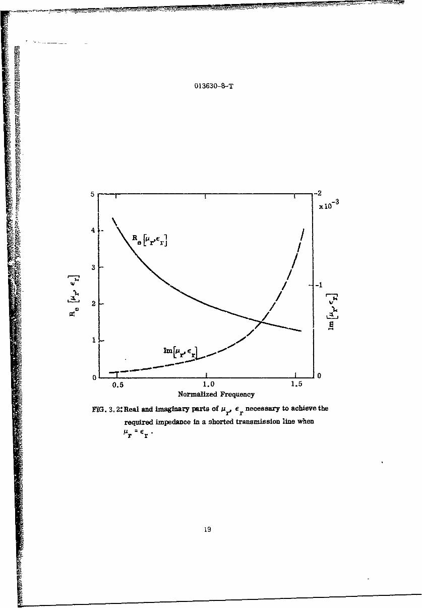
In Fig. 3-2, tie computed values are shown when pr -- r. Over the
frequency range considered (0. 5 to 1.5), the real part of p r = r canges from
about 4. 2 to !. 25 and the imaginary part (i. e. the loss) of pr = r changes from3 3 r
about 0. ix 10 3 to 1.3x I) - 3 . In Figs. 3-3 and 3-4, the results are presented
for g r = 2E and pr =2 r respectively. At firs" glance it appears that the
curvef. ip the two figures are the same except for interchanged M r and E . Anr
examination of the actual numbers, however, reveals that the curves are slightly
different and this can be seen by observing that in Eq. (3. 4) the impedance of the
cavity depends on both factors .fe and "J'IE , where the former is depen--r r r
dent on the ratio of pr to Cr and the latter (being a product of M r and Cr ) is no'.
As was the case for the problem treated in Section 3. 1, no real-life materials
that satisfy the demanded frequency variation appear to exist. In fact, the demands
on the material appear even worse here. Although materials are available whose
real parts resemble those required, they also possess imaginary parts of order unity
or grcacer. In contrast, for the computaions carried out, the imaginary parts of-l
or er must be of order 10 in the case of a radial cavity (Section 3. 1) and of
order 10 whcrx the load is transferred as a lumped element to the center and
realized by a TEM transmission Line (Section 3.2).
In the hope of requiring properties of dielecirie/magnetic materials that are
more realistic than those obtained above, cases were investigated where the trans-
mission line is terminated in loads other than Z = 0. To limit the number of
18
013630-8-T
Sf 1 -2x10-
$4
S2
1 T1
0.5 1.0 1.5Normalized Frequency
FIG. 3, 2: Real and imaginary parts of iA r cE necessary to achieve the
required impedance in a shorted transmission line when
Ar r

12 -
x 10-3
10-e
8 I -2
REM
01 1.
0.5 1.0 1.5
Normalized Frequency
FIG. 3. 3: Real and imaginlary p~arts of IYArP ncsar oahivrh
required imp-edance in a shorted transmission line when
Ar 2 E r
20

I rn e r
L- 4
err
4 -
0 0,
0.5 1.0 1.5Normalized Frequency
MIG. 3. 4 Real and imaginary parts of Ari Er necessary to achieve the
impedance in a shorted transmission line when Ir2 fY
21

013630-8-T
computations, the condition IAr = E was chosen, and computations were performed~rsimilar to those described above, but for terminations which were
a) resistive.
b) open circuit-
c) inductive,
and d) capacitive.
In all of the cases considered, the curves for jr and E resembled those shownr r
in Fig. 3-2: the real part decreased with frequency while the (small) imaginary
part (except when the load was resistive) increased. For a resistive load, the
required imaginary part was positive, implying an "active" material which is ob-
viously non-existent. Since the curves for the required p = E are so similarr= r
to those of Fig. 3-2, the appropriate curves will not be presented. but only the ratios
of max to min values of g r demanded over the 0.5 to 1.5 frequency range.rr
Such ratios may eventually be of interest, since for all known low-loss materials,
the permeability and permittivity are almost constant with frequency. The short
Z Max to Min Ratios of r=
Short 3.26
Open 3.53
Capacitive (C = 0.01 Farads) 3.27
Inductive (L = 24/r Henries) 3.26
circuit line appears to be the best of the cases considered, although the ratios for
inductive or capacitive loading are not much greater. Values of L and C other
than those used above were also examined, but the results were the same-the 3hort
circuited load still gave the smallest max to min ratio.
The unrealistic requirement on the variation of p r and E as a function ofr
frequency to produce zero back scattering is hardly surprising. As shown by
McMahon et al (1968), the required impedance crnnot be obtained using passive
lumped elements, and this would lead us to expect that passive distributed networks
22

L. b
would also be ineffective. Furthermore, if Re[Zn, = O. Foster's Reactance0.- Fote' Ratac
Theorem, stating that
aI
a >m0 , (3.6)
F where w is the angular frequency, applies also for distr;buted loads (Ramo and
Whinnery. 1958), and since the curve for the demanded impedance Z in Fig. 2-3
shows that
axm[zQ <f,< 0 , (3. 7)
it would appear that such a load cannot be realized using passive devices. How-
ever, the optimal Z does have a non-zero real part albeit small, and under
these conditions Foster's Reactance Theorem does not apply. It was for this rea-
son that we proceeded to determine the electric characteristics of materials
required for loading a coaxial cavity in the hope that the appropriate materials
might exist or eventually be realized.
23
17

013630-8-T
IV
CENTER LOADING
4. I Introduction
The impedance required at the center of a conducting body to achieve
cross section modification naturally differs from that required at the surface, since
a center load must be coupled to the surface through a radial transmission line.
However, the difference is quantitative rather than qualitative; the center load still
has the general behavior of a negative reactance. For the particular case of a sphere,
studied by Chang and Senior (1967), the required load can be well approximated by
2 2~s 4.0
SZ(s) = -K . 1O(4. 1)
• which for conyenienc-_ may be normalized to
2S -
Zfs) = - - (4.2)
The load may also be viewed as a reflection coefficient
Z - Z 20 s 4_~S 4- 1 (4 .3 )Z+Z 0 2
where Z_. has been normalized to unity. For s = i, we have
(4.4)
and = 2 tan 2 (4.5)i - 2
Although there is a one-to-one correspondence between load impedance and reflection
- oefficient, the reflection coefficient viewpoint is perhaps more appropriate to an
understanding of the mechanisms involved, since cross section reduction is achieved
basically by can -gn the phase of the current over a portion of the scatterer to obtain
cancellation of the seattered field in a orescribed djirection.
241

0 13630-8-7T
4.2 Reflection Coefficient Realization
In view of Eqs. (4-. 4) and (4.5), the loading rmay be viewed as a mechanism
for reflecting the incoming wave with its magnitude unchanged but with the phase
changed in a prescribed manner. One way in which this might be done is shown in
Fig. 4-1, where an ideal circulator is combined with an all-pass, phase-shift
Idealcirculator All-pass
S(,) phase-shift network
JFIG. 4-1: Reflection Coefficient Realization-
netwvork. Quite aside from the difficulty of realizing a broad-hand, high-frequency
circulator, this scheme is doomed to failure by a fundamental limitation of all-pass
networks. The transmission function of any ali -pazs network, piassive or active.
is of the general form
(s-)(s-s,)..
where the s. have positive real parts; in other words, there are poles in the lef~t
half plane, with zeros at the mirror-image right hali-plane points- The angle of any
rational function at any point - is the s-a of the angle Imaue n h sa
counterclo&kwise directiod) from all the zeros to so, Minas the sum of the angles
from the poles. When a function ha ving the form of Eq. (4.61j is evaluated on the jo
axis. the zeros are all to the right and the poles all to the left- Therefore, the zero,
angles are all decreasing, and the pole angles increasing, as frequency increases.
A stable all-pass fanction thus Mas a phase shift vuhich decreases with frequency; how-
ever, the phase-shifthfunction (Eq. (4t.5)) is an increasing- function o! freqnc~ny and
therefore cannot. be realized by an all-pass networ,..
25

013630-8-T
Minimum phase networks, having both poles and zeros in the left half s-plane,
can redil a o-hase shifts which increase with frequency. In this case, however, the
magnibde function cannot be maintained at a constant value. It must be concluded
therefore, that. the reflection coefficient to provide the desired reflection cannot be
realized by a passive network. An active realization based on the reflection coefficient
approach does nat appear to offer any advantage over a realization based on the impe-
dance appro;a-h, which is discussed below.
2_ 3 Impedance Realization
There are a number of active elements with the potential for realizing the
desired impedance given by Eq. (4. I). Some which have been considered and rejected
are di.zeussed below.
Pum:ned i-aractor diodes are known to exhibit input impedances not realizable
by _,ssive networks, which suggests their possible application to the problem at hand.
Unfortunaiiy, the variation of impedance with frequency is difficult to predict and
extremely difficult to control, since it depends on a relatively large number of para-
meters. While there may be cases for which varactor diodes provide a suitable load,
it is uniinely that the probability of success justifies the effort which would be involved.
Suitably-biased tunnel diodes yield a negative-resistance characteristic which
has been exploited in a number of active synthesis schemes. Since the negative
resistance is always shunted by a parasitic capacitance, tunnel diode realizations
aie mote limited ;n generality than some other active realizations. There is also
a severe stabiitv problem due to the pesence of lead inductance, which tends to
make the device self-resonant at some fairly high frequency. For these reasons, the
unne diode would appear to offer no advantage, and some disadvantages, when com-
;ared with other possible methods.
Two other possibilities which are worth mentioning are nonlinear and
adaptive realizations- Nonlinearity can be discarded immediately, since the
;trengh of t-he incident wave is not constant and a nonlinear load would, by definition,
na',' "a response dependent on signal amplitude.
2I

0 i363 u 0J -T
An adaptive loading scheme, in which the frequency of the incoming signal
is sensed and acts as the control signal for a discrete or continuous tuning system,
has some obvious advantages and disadvantages. Since a relatively large number
of load parameters can be made to vary more or less arbitrarily, almost any im-
pedance variation can be achieved. On the other hand, such a scheme would prob-
ably involve time delays on the order of milliseconds, which could be unacceptable
in some applications and would certainly be ineffective if the incoming signal were
broadband or swept in frequency. In any event, adaptive schemes were felt to be
outside the scope of our investigations and were not considered in any detail.
4.4 The Negative Impedance Converter
Of the active devices which are applicable to general synthesis techniques,
" ~.the one most suitable for the present problem would appear to be the Negative
Impedance Converter, or NIC.
The NIC is, of course, only one of many devices which have been used for
active synthesis. Of the other possibilities, the gyrator may be ruled out imnmedi-
ately, since the class of driving-point imoedance functions realizable with a gyrator
is also realizable with passive elements only (the gyrator does. h'owever, offer
advantages in transfer function synthesis). Realizations using controlled sources,
operational amplifiers, etc., handle the same class of functions as do NIC realiza-
tions and in fact frequently lead to networks embodying a N-C; there is thus no loss
of generality if these realizations are not treated separately.
4.5 MC Theory
The Negative Impedance Converter, or NIC, is a two-port with the property
that the impedance seen at cne port is the negative of the impedance erminaling the
other port. The .IC is most conveniently characterized by its h-parameters, which
have the general form
(4.7)I?] h h o
21
27

013630-8-T
With port 2 terminated by an admittance Y2' the input impedance is given by
Z, = h h 12221 (4.8)1 11 h 22+Y2
In order to operate as an NIC, the two-port must have the properties
h " = 0 (4.9)1 22
h h2 -1 . (4.10)
In )ractict_, the latter condition is normally satisfied by
h12 h 21 (4.10)
with the positive sign yielding a current-inverting NIC (INIC) and the negative sign
:1 x oltage inverting NIC (VNIC). Many NIC circuits have been given in the literature;
most of them are essentially realizations of one of t'E two circuits shown in Fig. 4-2,
where equivalent circuits for the ideal INIC and VNIC are shown.
1 C ViC_ +
V 1 V2 1 V2
0-- 0 -a) INIC b) VNIC
FiG. 4-2: Basic MIC Realizations.
Given an ideal NTC, the most obvious way of realizing the desired impedance
is to terminate the NIC with a series-resonant circuit. Quite apart from the usual
difficulties associated with inductors, such as losses and stray capacitance, this
scheme is generally unsatisfactory if the NIC is not perfect. Except at very low
fr'equencies, the conversion ratio of the NIC will normally be a complex function of
frequency; that is
28

013630-8-T
in Ai (4.I12rid k =a(w) + jb((i Zload
4Aii where a(j is negative and b( ) is small compared to a(&). A purely reactive load
jthen yields
Z. =(a+ jb) jY= -bYL+ jaYL (4.13)
which has an undesirable real component. If resistance is added to the load in an
attempt to compensate, the result is
z. = (a+Ib)(RIY) = (aRL - bYL)+J(aYL+bRL) • (4.14)in L L L L L L
The condition for making Zin purely reactive, namely
aR -bY, =0 (4.15)L L (.15
in general cannot be satisfied with RL > 0 over a frequency band in which YL
changes sign unless b changes sign simultaneously with Y Since b(w) cannot
normally be controlled to such an extent. compensation cannot be achieved with
this realization.
Fortunately, there exist realization techniques which not only avoid the use
of inductors but which also offer better potential for compensation. By subtracting
an appropriate positive resistance from the normalized Z(s) we obtain
22 _2 s 2+(a+ 1 s+lZ (z) = Z(s) -(a+ I s - (a+(
a a s
which has simple, negative-real zeros. Then, by expanding Y (s) as an RC admit-
tance, one obtains
y (s) as as (4.17)
(s+ )G -a2 ) (s~a)l(1-a 2 )
29

ULi3630-8-T
wher9. :.L Imis b~een assumed, without loss of generality, that a < 1. Since Y (s)
nlas b~en vxpressed as the difference of two RC admiittances, it can be realized
with an NIC. Adding on the constant originally subtracted leads to the final reali-
/.atto.i, snuwnf in Fig). 4-'1.
.2 2 2L1 -a 1-a
a I a- R a
Sa 2 21
1-a 1-a
FIG. 4-3: RC - NIC Realization of ZVs).
T!IJe dual procedure to the above approach also leads to a realization.
Subtracting a iuitaiie pubiti constant fromr Y(s) yields
_ _ _ _ _ __Y1 z) a ( s + a ) ( s +i a )y() a 2 (a 2(4- 18)
a- i+a ' s 2-1
-N n fotre Z (s) may be expanded as an IIC i mpedance, yielding
Z (s) - -aa { a2 a - /a }(4.19)aU-a
which iS the difference of two RC impedances and can therefore be realized using an
.NWI. The resulting realization is given in Fig. 4-4.
30

Wt
013630-8-T
SN
LR
with
1+a2 (1+a 2 (! 2 .a 2
R 0 R = R2 R 3 aa(i -aI a( -a
c-O+a2) 2 2- (1+ a 22
FIG. 4-4: Alternate RC - NIC Realization.
In both of the realizations above, the parameter a may be chosen anywhere
in the range 0 < a < 1, the choice being determined by stability, element-ralue spread,
etc. In practice, a value of a = 0.5 has proven to be a reasonable choice.
These realizations have an advantage over the LC realization in that the load
impedance of the NIC. and therefore the input impedance as well, remains in one
quadrant of the complex Z-plane. For example, in the first realization, as frequency
varies, the load impedance moves along a vertical line in the fourth quadrant, as
shown in Fig. 4-5a. With an ideal NIC. the input impedance would lie on a vertical
line in the second quadrant, as shown by the solid line. If the NIC is non-ideal, the
input impedance might have the form siiown by the dotted line, which would result
if the conversion ratio of the NIC had a phase angle which departed from 1800 at the
higher end of the frequency band. This effect could be compensated by changing the
31

E 03630-8-T
load im.oedance, as shown in Fig. 4-5b. Since the modified load-impedance locus
Inp;t Irepedance Compensated input
Z-plane Z-plane
I od-eea
Load Impedance opada) Uncompensated b) Compensated
FIG. 4-5: Effect of Lead Compensation.
lies entirely in the right-half Z-plane, it is reasonable to suppose that it could be
realized with passive elements. An attempt to apply this same technique to the LC
realization would lead, in general, to a compensated load-impedance locus which
crossed the Im-axis of the Z-plane and which would, therefore, be unrealizable
with passive elements.
Another realization is obtained by expanding the negative term in Eq. (4.17) in
the form
2as a a(4.20)
(s+a)(1-a 2 ) 1-a 2 (s+a)(I-a 2 )
which has the form of an RL admittance in parallel with a negative conductance.
This expansion leads to the realization shown in Fig. 4-6. Since the use of
inductance is generally undesirable and since it is generally somewhat more
32

ii! 0 i3630-8-T
R10
R R12 NIC R3
C L
with
a2 I-a 2 1-a 2 2
0 a I a 2 a 3 a
22a l-a
C 2I-a a
FIG. 4-6: Negative R1 Realization.
difficult wo compensate for NIC imperfections with a constant load, as opposed to a
load which is a function of frequency, the realization of Fig. 4-6 is not as useful as
those of Figs. 4-3 and 4-4.
3 4.6 INIC Circuits
A particularly simple NIC circuit is given in Fig. 4 7a. It is easily seen
LL
I IG 4-? olag ApfirnIC.
-Z
33

013630-8-T
that V = -V therefore
12 = -V2 /ZL = VI/VL (4.21)
and Z = = -Vl/I =ZL . (4.22)in 1' 1 12 L
The modified configuration oi Fig. 4-7b yields the same result and is somewhat
easier to achieve in practice; this configuration is not a true tv'o-port NIC, but it
is usable in the one-port application being considered here.
A non-inverting amplifier with a gain of 2 can be constructed using two
high-gain inverting amplifiers with negative feedback around each stage to give a
stage gain of F2 as shown in Fig. 4-8. Assuming that each amplifier has input
00
--
FIG. 4-8: Non-Inverting Amplifier.
and output impedances equal to R3 , and connecting a load admittance Y between the
input and outout terminals, the input impedance is found to be of the form
y a -bY (4.23)in c-dY
where a, b, c, and d are ositive constants. Letting
Y= b Y- (4.24)b L
which is equivalent to adding a shunt conductance G a/b. yields
34

K013630-8-T
d+ dY
+Z g (4.25)-bYL
Finally, adding a series resistance
R =d/b (.4.26)L
givesad + beZn=--_Z L . (4.27)
in b 2 L
This circuit was constructed using RCA CA 3004 widebaud amplifiers as the
active elements. Without the load, the circait operated sasfactorily as a non-
inverting amplifier, alth-gh it was more sensitive to v--riations in supply voltage
than might have been anticipated. When the load was added, the sensitivity became
extremely critical; the range of sdpply voltage over which the circuit exhibited NIC
action was only a few tenths of a volt, and there was a very strong tendency toward
high-frequency oscillation. Further development of the circuit was therefore dis-
continued.
Another MNC realization uses a differeutial-input, operational amplifier, as
shown in Fig. 4-9. Assuming that the amplifier has high gain and infinite input
-1+ +'1 +
£ FIG. 4-9: Operational Amplifier MGC.
I L
impedance. there is a virtual short at the input terminals, which impies that
I =V The two resistors thus have equal voltages across them, and sin"- the
V I1 2'
amplifier draws no input current we have I L,. satimfy-ing the conditions for
NIC operation.
V 35

For low-freqnency operation. this circuit is quitz attractive, since suitable
operational amplifiers are readily availabie in tntegrated form. Howevrer, a num-
ber of undesirable effects are observed as frequency is i-2creased. The inout impe-
dance can no longer be assumed to be infinite, due to !he presenee of shnt capacitance.
The Impedance between the two input termIinals daoes not seriously degrade perfor-
manice. since the in.puts are at approximtely rcqual, potentials. The Imzpedance
between each input and ground cancel one another by NC action provided that the
circuit operates as a perfect NIC with unit conversion ratioc.
Another high-frequency effect is the variation of ampfifier gain in both
magnitude and phs.The atter is the =~ore important factor since in general
phase -shift becomes appreciable at frequenries a decade below the 3 dB point. In
order to maintain stability and ininize aoise, commercially available operational
amplifiers generally have a controlled gain toll-off at a relatively low frequency,
making them unsuitable for the proposed applicatior- at frequencies much n excess
of 1 Mz.
In order to be able to more readily make circuit modifications, a b-.eadboaxrd
amplifier was constructed using a conventional. difmreatiai input stage driving a
common-emitter stWg. A variety of compensation schemes were tried. using
frequency-dependent coupling and/or fee&-ack netwo-ks, etc..- ic an attempt to
achieve zero phase-shift along with reasonably flat gain. Although tbis goal was
realized, the cost in gain reduction was prohibiti m; the compensation reduced the
gain to less than 10 dB. Additional stages to increase gain also introduced undesir-
able phase shift- It was concluded that the operational amplifierNMC was not Suitable
for high-frequevzy operation. This conclusion -is subject to modification by state-
of-the-art developrments in operational amplifier technology, although It is difficult
to be opti"mistic about the possibility of obtaining hih gain, zero phase-shift, and
highn input impedance in the VHF range-
IThe Yanapisaa NC
The NIC circuiit which gave the best experimental results was described
originalfly by Yanagisawa (1957). The circuit is shown iL Fig. 4 -. 0 In simplified
3U

I
I
-i -t 2
V2
FKG. 4-10: Yanagisawa NM.
I form. with al! bas and compensation ircuits omitted- Assuming that V = 0
in both transistors. we h- ve V, = V, . Further assuming that a = 1, all of I I
flows through R, - developing a voltage Ri I , which als-o, appears across R 2.- Theemier current of Q is therefore iLRI'R sin-ce both base currents are assumed
- zero. this is also the value of We have, therefore
SV. := V (428a)
2R-
12 = R._, t.28b)
which describes a NC with
R
Zi -- Z . 1%4.29)_in L
in practice, of course, each transistor must have a coUector supply circuit;
however, if these are identical and the NIC conversion factor is -i, then the col-
lector impedances cancel one anoher, since one is across the input and the other
across the output fo. AC.
37
-I r m m
013630-8-T
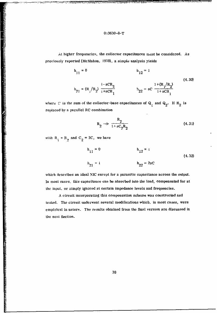
At higher frequencie:s. the collector capacitances rast be considered. As
previously reported (McMahon, 1970), a simple analysis yields
h =0 h -ih! ! 12
(4.30)= (R/R.) h sc
h1 i - 1 sCR i 22 i sCR
1 22
where; C is the sum of the collector-base capacitances of Q I and Q 2 " If R 2 is
replaced by a parallel RC combination
R9R2 (4.3 i)
with R= R9 and C, 2C, we have
hi =0 h211 12
(4.32)
"21 2h9 . =2sC
which describes an ideal NIC except for a parasitic capacitance across the output.
In most cases, this capacitnce can be absorbed into the load, compensated for at
the inout. or simply igno-red at certain impedance levels and frequencies.
A circuit incorporating this compensation scheme was constructed and
te, sted. The circuit underwent several modifications which, in most cases, were
empirical in nature. The results obtained from the final version are discussed in
the next Section.
38

013630-8-T
IV
EXPERIMENTAL RESULTS
5.1 Measurement Techniques
IC circuits in general have one open-circuit stable (OCS) port and one
short-circuit stable (SCS) port; the device is stable if the impedance loading the
OCS port is sufficiently large and that at the SCS port sufficiently small. It was
therefore necessary to have two different measuremept schemes available to ac-
comodawe the loading requirements of the two different Orientatons.
Fig. 5-1 shows the measurement scheme using a General Radio 1606-A
RF Impedance Bridge, which presents a high impedance to the load. The'oscil-
loscope was used to monitor for distortion and possible oscillations, but was
removed during the actual measurement.
A low-impedance (50 <2) measurement scheme using an HP Vector Voltmeter
is illustrated in Fig. 5-2. The VVM compares the incident voltage, E., at theI
50.Q load with the total voltage, E. + E . at the NIC; the qantity actually measured1r
is thus I +p. which is easily converted to values of Z by use of a Smith Chart or
a simple calculation. The system is first calibrated using a short-circuit load in
order to compensate for differing line lengths and other sources of undesired phase
shift.
The actual NIC circuit and its load are shown in Fig. 5-3. The NIC itself is
basically the Yanagisawa circuit of Fig. 4-10 with the addition of biasing. it was
found necessary to add the 27 K resistor between t' a two bases in order to obtain
reliable turn-on of both transistors; without this resistor, the circuit has a stable
state in which both transistors are cut off. To improve stability, the gain is
deliberately rolled off at frequencies above 10 MHz by means of the RC circuit in
:ie collector lead of Q.. while phase-shift is controlled bv the emitter of Q. The
6. 8 K resistor at the input and the 10 P_ resistor at the output are for adjustment
of impedance levels.
The conversion ratio. Zin/Zload of the NIC was first measured with a 100 IT?
load. with the results shown in Table 5. 1. As intended, the ratio drooped markedly
above i0 MHz, falling to -. 470+j.020 at 15 MHz.
39V

01 3630-8-T
Oscilloscope NCPwr Heath IP-27
FIG.llator RF Bridge Masreoent(voltmter nll deector
I~t
1 A
Sh rt C rc i
GR~~~H 130 R10- P8405A
Noter Volmee read
FIG. 52: Volage Relectio Mto VSoyncnd
FIG.~o I-mpeBrdeZ Measurement.
EB irB
P~op Pro0

01 3 630-8-T
Q00
C. "
0 00 0d
00~4
Cc))
r-4 I-f 4
c~J 0
U")
to0
141
013630-8-T
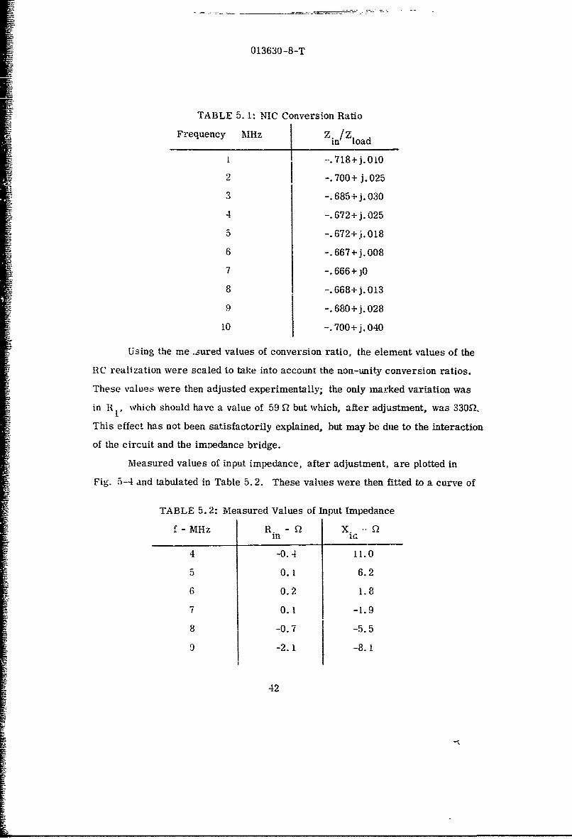
TABLE 5. 1: NIC Conversion Ratio
Frequency MHz I in /Zlad
it -. 718+j.oo
2 I -. 700 + j. 025
3 -. 685 + j. 030
4 -. 672+ j. 025
5 -. 672+).018
6 -. 667 + j. 008
7 -. 666+j0
8 -. 668+j. 013
9 -. 680 + j. 028
10 -. 700 + j. 040
Using the me .sured values of conversion ratio, the element values of the
RC realization were scaled to take into account the non-unity conversion ratios.
These value- were then adjusted experimentally; the only marked variation was
in RI which should have a value of 59 2 but which, after adjustment, was 330Q,
This effect has not been satisfactorily explained, but may be due to the interaction
of the circuit and the impedance bridge.
Measured values of input impedance, after adjustment, are plotted in
Fig. 5-4 and tabulated in Table 5.2. These values were then fitted to a curve of
TABLE 5. 2: Measured Values of Input Impedance
f-MHz R. - Q X. -.-Qi n
4 -0.4 11.0
5 0.1 6.2
6 0.2 1.8
7 0.1 -1.9
8 -0.7 -5.5
9 -2.1 -8.1
42

013630-8-T
30
25 imaginary Comp. Z .
Real Component z
20-
151
.' 5
bp
C"2 -5
-10 - a 0.1
-15 -f a5 LIHz
Real Zj < 1Sfor 4<f< 8 MHz-20 . I I 1
1 2 3 4 5 6 7 8 '9 10Frequency MItz
FIG. 5-4: NIC and Load Bridge Measured Impedace.
43
I

0:3630-8-T
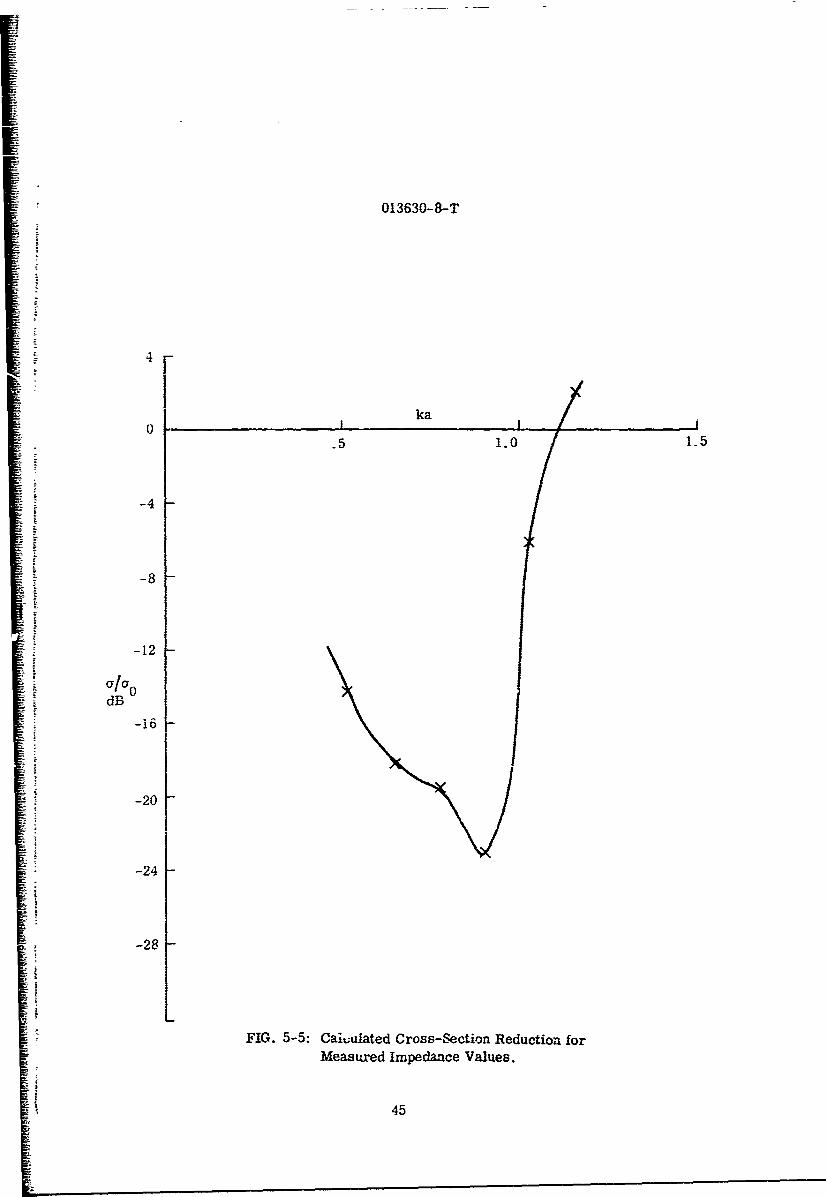
optimum impedance by choosing a frequency denormalization such that ka = 0. 513
at 4 MHz. with a slot width, 6, of 0.09. The cross section reduction was then
calculated. with the results given in Table 5.3 and Fig. 5-5.
TABLE 5.3Calculated Values of Cross Section Reduction
ka a/a 0 - dB
0.513 -14.42
0.642 -18.23
0.770 -i9.40
0.898 -23.08
i.027 -6.09
1.155 +2.12
No attempt was made to optimize the fit, on the grounds that the precision
of the measurements did not justify such a procedure. Even so, a cross section
reduction of 13dB or better was achieved over an approximate 2:1 frequency range
irom ka = 0.5 tc ka = 1. 0. Since no previous experimental results have shown
bandwidths of more than a few per cent. this is a significant lesult which verifies
the basic suitability of the NIC realization. Admittedly, the frequency range is
lower than that originally aimed for, but this is a result of state-of-the-art limita-
L1&fs or !ransisto-s and ci, cuit construction techniques rather than any fundamental
limitation o" the realization technique itself.
44
013630- 8-T
ka
-51.0 1.5
-4
-8
-12
dB
-20
-24
-28
FIG. 5-5: Cahadlated Cr038-Section Reduction forMeasured Impedaace Values.
45

013630-8-T
Vi
PROSPECTS FOR FURTHER DEVELOPMENT
From an evaluation of the results presented in this report, it appears that
neither the lumped nor the distributed passive loads would provide the required
impedance variation for broadband cross secticn control. The only alternative is
thus the use of active devices, and of these the Yanagisawa NIC circuit could al-
most certainly be made to operate at higher center frequencies by using transistors
with higher f Is, although stability would very likely present difficulties. In con-
junction with more sophisticated circuit techniques (e.g.. strip line), an order of
magnitude increase in frequency might be achieved. The requirements are stringent,
however; a transistor with A = 100 and fT = 2 GHz, for excample, has a beta-cutoff
frequency of 20 MHz and exhibits significant phase shift at 2 MHz. Compensation
might make such a transistor usable at frequencies as high as 20 or 30 MHz, but
it is obvious that substantial improvement in performance must await major develop-
ments in transistor technology: f Ts of 10 GHz or more, with reasonably large /'s.T
Another possibility would be to develop a circuit which exhibits some degree
of N!C action in the desired frequency range, however imperfectly, and then use
load compe.-sation to achieve the desired result. Since there is no well-developed
theory of synthesis with imperfect active devices, this would be primarily an empir-
ical procedure, with no guarantee that the required load compensation would be
realizable. However, this approach would seem to be worth some further consider-
ation.
Integrated-circuit technology could contribute most to this problem through
development of a true VHF operational amplifier. The op-amp is one of the com-
monest linear IC's available, and rapid advances in performance are being made.
If a differential-input amplifier with high gain, high input impedance, and low out-
put impedance at VHF should become available, the configuration of Fig. 4-9 should
be useful.
46
E

01 36 30-8-T
Finally, since the necessary amplifiers are preseutly available in integratedform, the circuit of Fig. 4-8 warrents further study. This circuit has very severestability problems, but perhaps a way to overcome them might be found.
47

013630-8-T
REFERENCES
As, B. 0. and H. J. Schmitt (1958) "Back Scattering Cross Section of ReactivelyLoaded Cylindrical Antennas", Harvard University Cruft Laboratory Sci-entific Report No. 13.
Chang, S. and T. B.A. Senior (1967) "Study of Scattering Behavior of a Spherewith an Arbitrarily Placed Circumferential Slot". The University of Mich-igan Radiation Laboratory Repoit No. 5548-6-T.
Chen, K-M (1965) "The Minimization of Back Scattering of a Cylinder by DoubleLoading" The University of Michigan Radiation Laboratory Report No.5548-4-T.
Chen K-M (1968) "Minimization of Radar Cross Sections of Cylinders by Compen-sation Method". Scientific Report No 1, Division of Engineering Research,Michigan State University.
Chen, K-M and V.V. Liepa (1964) "The Minimization of the Radar Cross Sectionof a Cylinder by Central Loading". The University of Michigan RadiationLa:)oratory Report No. 5548-1 -T.
Hu Y-Y (0968) "Backscattering Cross Section of a Center-Loaded Cylindrical
Antenn-a". ERE Trans. AP-6. 140-1--8.
Iams, H.A. ( 1950) "Radio Wave Conducting Device", U.S. Patent No. 2. 578,367.
King. R-W_ P. (1956) The Theory of Linear Antennas. Harvard University Press.Cambridge. Massachusetts.
MeMahon, E_ L. (i969) "Computed Cross Section Reduction for Various Loads".The University of Michigan Radiation Laboratory Internal MemorandumNo. 01363-511-M.
McMahon. E. L_ (197C) "Circuit Reaiization of Impedance Loading for Cross Sec-tion Reduction". The University of Michigan Radiation Laboratory ReportNo. 01363-7-T.
McMahon E_ L.. A.R. Braun and R. S. Kasevich (1968) "Network Theory Problemsin Imnedarce Leading"- The University of Michigan Radiation LaboratoryReport No. 5548-d-T.
Liepa. V.V. and T. B.A. Senior (1964) "Modification to the Scattering Behaviorof a Sphere by Reactive Loading". The University of Michigan RadiationLaboratory Report No. 5548-2-T.
LiepaV. V. and T B.A. Senior (1966) "Theoretical and Experimental Study of theScattering Behavior of a Circumferentially Loaded Sphere". The Universityof Michigan Radiation Laboratory Report No. 5548-5-T.
48

013630-8-T
Senior. T. B.A. and E. F. Knott (1967a) "Research on Resonant Region RadarCamouflage Techniques - Third Interim". The University of MichiganRadiation Laboratory Report No. 8077-3-T, AD 380204. SECRET.
Senior, T. B.A. and E F. Knott (i967b) "Research on Resonant Region RadarCamouflage Techniques - Fourth Interim", The University of MichiganRadiation Laboratory Report No. 8077-5-T. AD 382138. SECRET.
Ramo, S. and J.R. Whinnerv (i958" Fields and Waves in Modern Radio, JohnWiley and Sons, Inc., New York, Second Edition.
Sletten, C.J., P. Blacksmith, F. S. Holt and B.B.Gorr (1962) "',eductionof Radar Scatter Zrom Resonant Objects by Reactive Loading", AirForce Cambridge Research Laboratories Report AFCRL 62-754.
Smit, J. and H.P.J. Wijn (1969) Ferrites, John Wiley and Sons, Inc., New York.
Vincent, M. C. and K-M Chen (1968) "Experimental Investigation of the Modifi-cation of the Backscattering Cross Section of Metallic Objects", ScientificReport No. 5, Division of Engineering Research, Michigan State University.
Yanagisawa, T_ (1957) "RC Active Networks Using Current Inversion TypeNegative-Impedance Converters", IRE Trans. CT-4, 124-131.
!I
I4