Issue 19Fourth Quarter 1995
GENERALFawcett: 100,000+ Gates ......................... 2Guest Editorial .......................................... 3Customer Success Story ........................... 7New Product Literature ............................ 8Upcoming Events ..................................... 8Financial Results ....................................... 8What’s New at WebLINX? ........................ 9One-Day XACTstep Classs ....................... 9Component Availability Chart ........... 10-11Alliance Program Chart ..................... 12-13Alliance Contact Chart .......................... 13Development Systems Chart ................. 14Programming Support Charts ............ 15-17Impressive Reliability Results ................. 18Xilinx Earns ISO 9002 Certification ....... 18
PRODUCTSXC8100 Shines in 6502 Test ................. 19Introducing XC9500 CPLD Family! ... 20-21XC5200 Family Volume Production .. 22-23XC3100A-09 World’s Fastest FPGA ...... 22More Hi-Rel Versions of XC4000 .......... 243.3 V Survey Contest Winner ................ 24
DEVELOPMENT SYSTEMSUpdate on Logic Synthesis ................ 25-26XACTstep Direct From CD-ROM ....... 26-27
HINTS & ISSUESSynchronous RAM and Speed ........... 28-29Synchronous RAM Timing ................. 30-31Sensitivity to Power Glitches ................. 32Readback in FPGAs ........................... 32-33XC4000 Well Suited to 3.3 V ................ 33Minimizing Power Consumption ........... 34User-Defined Schmitt Triggers ............... 34Reconfigurable Computing Program ..... 35Technical Support Facilities ................... 35Applications Update .......................... 36-37Questions & Answers ........................ 38-394Q95 Fax Response Form ..................... 40
The ProgrammableLogic CompanySM
Inside This Issue:
T H E Q U A R T E R L Y J O U R N A L F O R X I L I N X P R O G R A M M A B L E L O G I C U S E R S
R
XCELLGENERAL FEATURES
XCELL On The WebThis journal, as well as a wide range of literatureabout Xilinx products, job opportunities, trainingschedules and much more are available onWebLINX, the Xilinx World Wide Web site...
See Page 9
PRODUCT INFORMATION
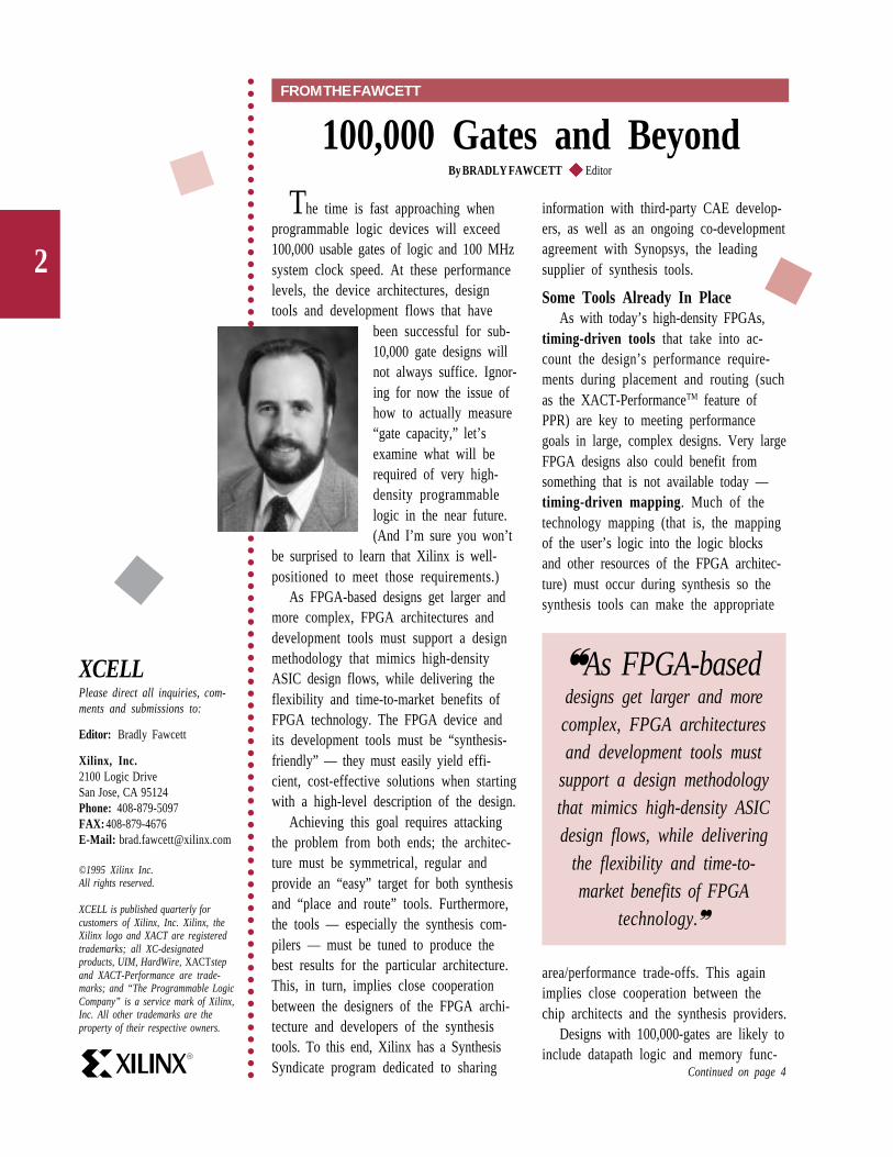
Family of In-SystemProgrammable
CPLDs IntroducedThe high-performance XC9500 CPLDfamily features FastFLASHTM, offering
exceptional ISP capabilities ...
See Page 20
Run XACTstepTM Direct From CD!
Complete instructions on running XACTstep version 6 aloneor in conjunction with Viewlogic’s PRO Series...
See Page 26
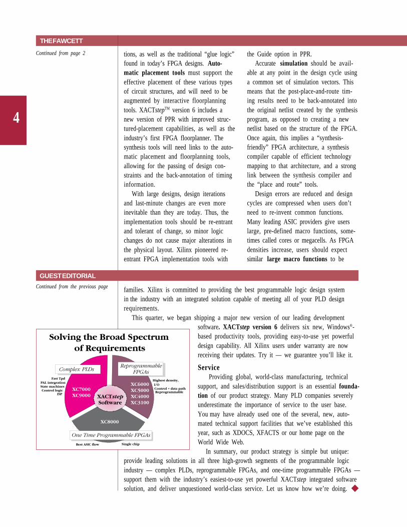
DESIGN TIPS & HINTSSynchronous RAM
Timing in the XC4000ETaking advantage of the XC4000E family’ssynchronous memory mode makes it possibleto operate near maximum clock frequency...
See Page 30
FROM THE FAWCETT
100,000 Gates and BeyondBy BRADLY FAWCETT Editor
R
XCELLPlease direct all inquiries, com-ments and submissions to:
Editor: Bradly Fawcett
Xilinx, Inc.2100 Logic DriveSan Jose, CA 95124Phone: 408-879-5097FAX: 408-879-4676E-Mail: [email protected]
©1995 Xilinx Inc.All rights reserved.
XCELL is published quarterly forcustomers of Xilinx, Inc. Xilinx, theXilinx logo and XACT are registeredtrademarks; all XC-designatedproducts, UIM, HardWire, XACTstepand XACT-Performance are trade-marks; and “The Programmable LogicCompany” is a service mark of Xilinx,Inc. All other trademarks are theproperty of their respective owners.
2
Continued on page 4
The time is fast approaching whenprogrammable logic devices will exceed100,000 usable gates of logic and 100 MHzsystem clock speed. At these performancelevels, the device architectures, designtools and development flows that have
been successful for sub-10,000 gate designs willnot always suffice. Ignor-ing for now the issue ofhow to actually measure“gate capacity,” let’sexamine what will berequired of very high-density programmablelogic in the near future.(And I’m sure you won’t
be surprised to learn that Xilinx is well-positioned to meet those requirements.)
As FPGA-based designs get larger andmore complex, FPGA architectures anddevelopment tools must support a designmethodology that mimics high-densityASIC design flows, while delivering theflexibility and time-to-market benefits ofFPGA technology. The FPGA device andits development tools must be “synthesis-friendly” — they must easily yield effi-cient, cost-effective solutions when startingwith a high-level description of the design.
Achieving this goal requires attackingthe problem from both ends; the architec-ture must be symmetrical, regular andprovide an “easy” target for both synthesisand “place and route” tools. Furthermore,the tools — especially the synthesis com-pilers — must be tuned to produce thebest results for the particular architecture.This, in turn, implies close cooperationbetween the designers of the FPGA archi-tecture and developers of the synthesistools. To this end, Xilinx has a SynthesisSyndicate program dedicated to sharing
information with third-party CAE develop-ers, as well as an ongoing co-developmentagreement with Synopsys, the leadingsupplier of synthesis tools.
Some Tools Already In PlaceAs with today’s high-density FPGAs,
timing-driven tools that take into ac-count the design’s performance require-ments during placement and routing (suchas the XACT-PerformanceTM feature ofPPR) are key to meeting performancegoals in large, complex designs. Very largeFPGA designs also could benefit fromsomething that is not available today —timing-driven mapping . Much of thetechnology mapping (that is, the mappingof the user’s logic into the logic blocksand other resources of the FPGA architec-ture) must occur during synthesis so thesynthesis tools can make the appropriate
area/performance trade-offs. This againimplies close cooperation between thechip architects and the synthesis providers.
Designs with 100,000-gates are likely toinclude datapath logic and memory func-
As FPGA-baseddesigns get larger and morecomplex, FPGA architecturesand development tools must
support a design methodologythat mimics high-density ASICdesign flows, while delivering
the flexibility and time-to-market benefits of FPGA
technology.
R
GUEST EDITORIAL
3
A Unique Product Strategyby CHUCK FOX Vice President, Product Marketing
Xilinx is the world’s largest supplier of programmable logic — approximately50 percent larger than the second-largest supplier. We achieved that leadingposition through a continuing commitment to providing a complete productsolution. This encompasses a focus on all three critical areas of the high-densityPLD product solution triangle: components, software and service.
ComponentsIn components, we will continue to leverage new deep submicron process
technologies aggressively to deliver improvements in speed, density and cost.We will combine this with innovative, targeted product families in all threemajor technology segments — CPLDs, reprogrammable FPGAs and one-timeprogrammable FPGAs — supported by the industry’s only seamless, no-riskcost-reduction path — the mask-programmed HardWire LCA. Each of thesehigh-growth PLD technologies serves unique requirements in the industry.
Xilinx is the only supplier to deliver leading solutions in all three of thesehigh-growth technologies. Our strategy is to continue to invest heavily in theresearch and development of innovative solutions in each area. Recently, we haveintroduced new solutions in all three.
The XC6200 family of reprogrammable FPGAsprovides extremely fast, in-system configurationspeeds (as low as 40 ns/cell) and a unique, high-speed dedicated microprocessor interface. Thesefeatures are ideal for using FPGAs in high-speed“reconfigurable coprocessing” applications.
The XC8100 series of one-time programmableFPGAs, featuring the industry’s first Sea-of-GatesFPGA architecture, is based on a proprietary metal-to-metal antifuse technology called MicroViaTM that,when combined with a unique, fine-grained cellarchitecture, delivers a powerful, single-chip FPGAsolution optimized for an ASIC-like design flow.
The XC9500 series of CPLDs is the industry’s first 5V FLASH solution, representingthe next generation in In-System Programmable (ISP) capability. This CPLD family deliv-ers a superior ISP capability targeted at today’s total product life cycle requirements.
SoftwareIn software, our open systems strategy means we provide seamless integration
into all the leading EDA environments, supporting popular front-end HDL, schematic,and simulation systems (as opposed to shipping our own proprietary front-end) aswell as supporting industry standards such as EDIF, VHDL, Verilog-HDL and ABEL.We combine this with our comprehensive back-end XACTstepTM tools to provide acompletely technology-independent design system supporting all our component
Continued on the next page
4
GUEST EDITORIAL
Continued from the previous page families. Xilinx is committed to providing the best programmable logic design systemin the industry with an integrated solution capable of meeting all of your PLD designrequirements.
This quarter, we began shipping a major new version of our leading developmentsoftware. XACTstep version 6 delivers six new, Windows®-based productivity tools, providing easy-to-use yet powerfuldesign capability. All Xilinx users under warranty are nowreceiving their updates. Try it — we guarantee you’ll like it.
Service Providing global, world-class manufacturing, technical
support, and sales/distribution support is an essential founda-tion of our product strategy. Many PLD companies severelyunderestimate the importance of service to the user base.You may have already used one of the several, new, auto-mated technical support facilities that we’ve established thisyear, such as XDOCS, XFACTS or our home page on theWorld Wide Web.
In summary, our product strategy is simple but unique:provide leading solutions in all three high-growth segments of the programmable logicindustry — complex PLDs, reprogrammable FPGAs, and one-time programmable FPGAs —support them with the industry’s easiest-to-use yet powerful XACTstep integrated softwaresolution, and deliver unquestioned world-class service. Let us know how we’re doing.
THE FAWCETT
tions, as well as the traditional “glue logic”found in today’s FPGA designs. Auto-matic placement tools must support theeffective placement of these various typesof circuit structures, and will need to beaugmented by interactive floorplanningtools. XACTstepTM version 6 includes anew version of PPR with improved struc-tured-placement capabilities, as well as theindustry’s first FPGA floorplanner. Thesynthesis tools will need links to the auto-matic placement and floorplanning tools,allowing for the passing of design con-straints and the back-annotation of timinginformation.
With large designs, design iterationsand last-minute changes are even moreinevitable than they are today. Thus, theimplementation tools should be re-entrantand tolerant of change, so minor logicchanges do not cause major alterations inthe physical layout. Xilinx pioneered re-entrant FPGA implementation tools with
the Guide option in PPR.Accurate simulation should be avail-
able at any point in the design cycle usinga common set of simulation vectors. Thismeans that the post-place-and-route tim-ing results need to be back-annotated intothe original netlist created by the synthesisprogram, as opposed to creating a newnetlist based on the structure of the FPGA.Once again, this implies a “synthesis-friendly” FPGA architecture, a synthesiscompiler capable of efficient technologymapping to that architecture, and a stronglink between the synthesis compiler andthe “place and route” tools.
Design errors are reduced and designcycles are compressed when users don’tneed to re-invent common functions.Many leading ASIC providers give userslarge, pre-defined macro functions, some-times called cores or megacells. As FPGAdensities increase, users should expectsimilar large macro functions to be
Continued from page 2

5
available as building blocks for FPGAdesigns. Similarly, “user-customizable”macro functions, such as those found inthe X-BLOXTM library, will ease thedesigner’s task. Ideally, such macros willbe inferred during the synthesis process inorder to preserve the portability of thehigh-level design description, as opposedto having to be specifically instantiated inthe HDL code .
Synthesis Friendly ArchitectureThe features that make an FPGA archi-
tecture “synthesis-friendly” include regular-ity, symmetry and granularity.
In many ways, the choice of logic blockgranularity is a trade-off between utiliza-tion and performance. With a smallerblock, less of each block is wasted for agiven logic function, but performancesuffers because more levels of logic areneeded for a given large function. Ofcourse, other factors also play a role. Forexample, configuration information mustbe supplied to each cell; a very fine-grained cell can increase the number ofconfiguration elements per usable gate.The “ideal” ratio will vary with the sizeand type of configuration element (SRAMcells versus antifuses, for example). So, forFPGAs, it’s more appropriate to think interms of a “sea-of-blocks” rather than a“sea-of-NAND-gates”.
For SRAM-based FPGAs, past experi-ence has shown that 4-input lookup-tablesare among the most-efficient logic struc-tures; this is not likely to change as FPGAsincrease in size. Synthesis algorithms thattarget lookup-table-based architectureshave become more efficient. The lookup-table approach also has the benefit ofincreasing routing flexibility due to itssymmetric nature; that is, signals can befreely swapped among the inputs to thetable merely by making the correspondingchanges to the contents of the memorycells in that lookup table. Thus, one likelycandidate for the “basic logic block” in a
high-capacity, synthesis-friendly, SRAM-based FPGA is the lookup-table/flip-floppair already common to several XilinxFPGA families.
Memory/Logic IntegrationAs stated before, large designs typically
need to integrate both memory and logicfunctions. The on-chip memory capabil-ity pioneered in the XC4000 family willcontinue to be a desirable feature for veryhigh-density FPGAs. There are three waysof implementing memory in an FPGA:• small, distributed blocks that can be
used as memory or lookup-table-basedlogic (as in the XC4000 architecture),
• larger embedded blocks of dedicatedmemory, or
• configuration memory cells that canoptionally be used as contiguousmemory in the end application (as inthe XC6200 architecture).Each approach has its advantages and
disadvantages, and future FPGAs are likelyto offer at least one if not some combina-tion of these options.
ConnectionsThe performance of programmable
routing resources is more dependent onthe number of programmable switchesthat must be traversed along a signal paththan the length of the metal lines. How-ever, it is wasteful both in terms of re-source allocation and overall performanceto use a long metal segment for a shortpoint-to-point connection. Thus, the pro-grammable routing resources in a largeFPGA should be segmented and hierar-chical in nature, with a mix of local(short), mid-range, and long metal lines.While the amount of local interconnectsurrounding a block does not need tochange as the logic array grows, the num-ber of longer interconnect lines shouldincrease. A good analogy can be made tothe layout of streets in a growing city; thesize and relative density of local streets
Continued onthe next page
6
THE FAWCETT
Continued from theprevious page
does not need to change dramatically asthe city gets larger, but the size and num-ber of freeways and major highways mustgrow with the city.
General-purpose routing resources needto be complemented by dedicated, global,low-skew nets for distributing clocks andsimilar high fan-out control signals. As arule of thumb, the clock distributionscheme should provide for a worst-caseclock skew that is less than 5 percent of theclock period (for example, less than 0.5 nsfor a 100 MHz clock).
Internal three-state buffers that providethe capability of implementing bi-direc-tional and multiplexed busses within theFPGA, as pioneered in the XC3000 andXC4000 architectures, will remain a criticalarchitectural feature for larger FPGAs. The
need for efficient, on-chip bus-sing will become more acute as32-bit and 64-bit busses becomemore common in microprocessor-based systems.
As FPGA gate capacity in-creases, the number of input/output pads also needs to in-crease. However, the ability toimplement larger designs in asingle device will eliminate theneed to partition designs among
multiple FPGA devices, which will reduceI/O needs to a large degree. Input andoutput buffers will need to be compatiblewith a wide variety of signaling standards(for example, JEDEC 3.3V, 5V TTL, 5VCMOS and GTL) to facilitate interfacing tomost available IC technologies. Time-to-market demands may cause the user tofreeze the I/O placement early in the designcycle, allowing the FPGA design and PCBlayout to proceed in parallel. Thus, abun-dant routing between the I/O blocks andlogic array will be required to ensure flex-ibility in pin placement during design itera-tions. Furthermore, as with current Xilinxfamilies, maintaining the same package“footprint” across several family members
will give system designers the option ofmoving to higher or lower density deviceswithout modifications to the PCB layout.
PowerHigh gate capacities and clock rates
mean greatly increased power con-sumption. The next generation of largeFPGAs probably will be based on the 3.3 Vpower standard. The transition to 3.3 Vlogic decreases dynamic power dissipationby 56 percent as compared to a 5 V devicerunning the same design at the samespeed. Circuit design techniques that mini-mize the turn-on overlaps of the P- and N-channel transistors in a CMOS device willbe employed to further reduce powerconsumption. Of course, advanced packag-ing with good thermal conduction charac-teristics also will be required.
Both the architecture and underlyingtransistor-level implementation of a high-density FPGA family should be “scaleable”to take advantage of future improvementsin IC fabrication technology. Again, Xilinxhas a strong track record in this regard, asprocess advancements have led to faster,larger, and less expensive devices in estab-lished FPGA families, such as those basedon the XC3000 and XC4000 architectures.
On Toward One MillionWhile there is plenty of life left in the
evolution of Complex PLD architectures (asevidenced by continuing advancements inthe Xilinx CPLD product lines), for the nearterm, PAL-like architectures cannot deliver theflexibility, density, or ASIC-like design flowneeded for designs exceeding 100,000 gates.
Meeting the requirements of designsover 100,000 gates will require more thanjust larger versions of today’s devices andtools. Using the highly-successful XC4000and XC5000 architectures as a steppingstone, Xilinx is poised to deliver newFPGA solutions that fulfill all the require-ments for very high density designs.
And we’re already thinking about onemillion gates...
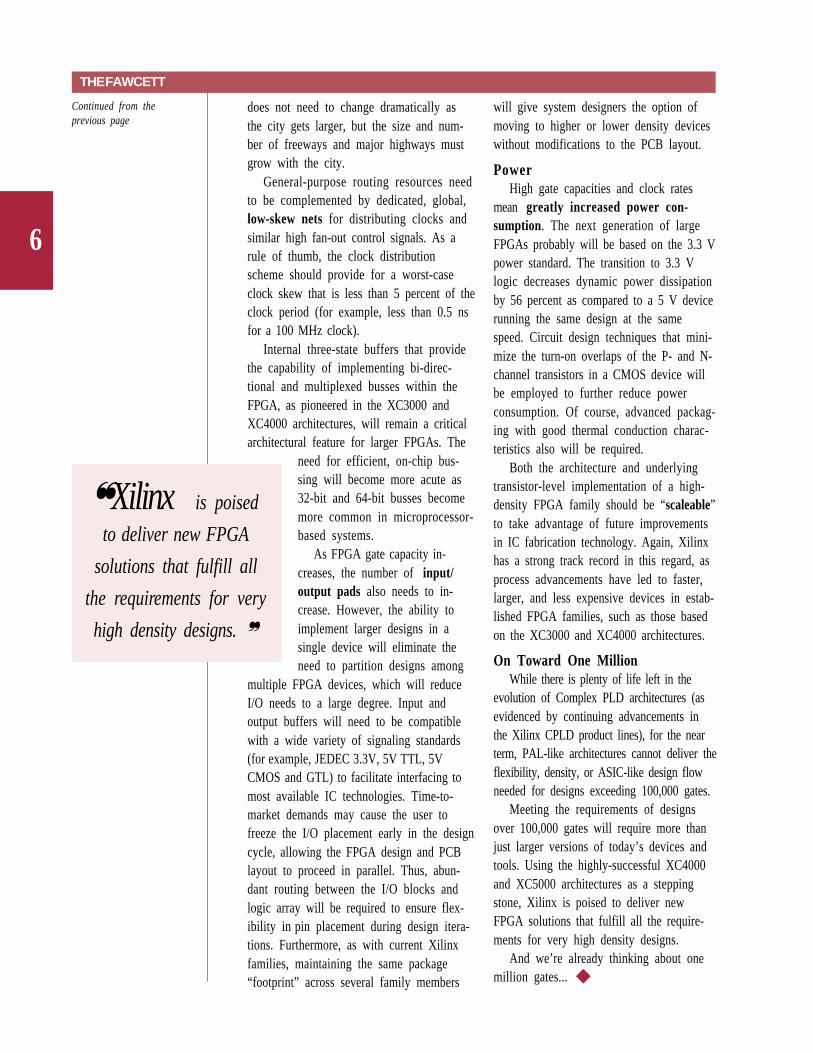
Xilinx is poised
to deliver new FPGA
solutions that fulfill all
the requirements for very
high density designs.
7
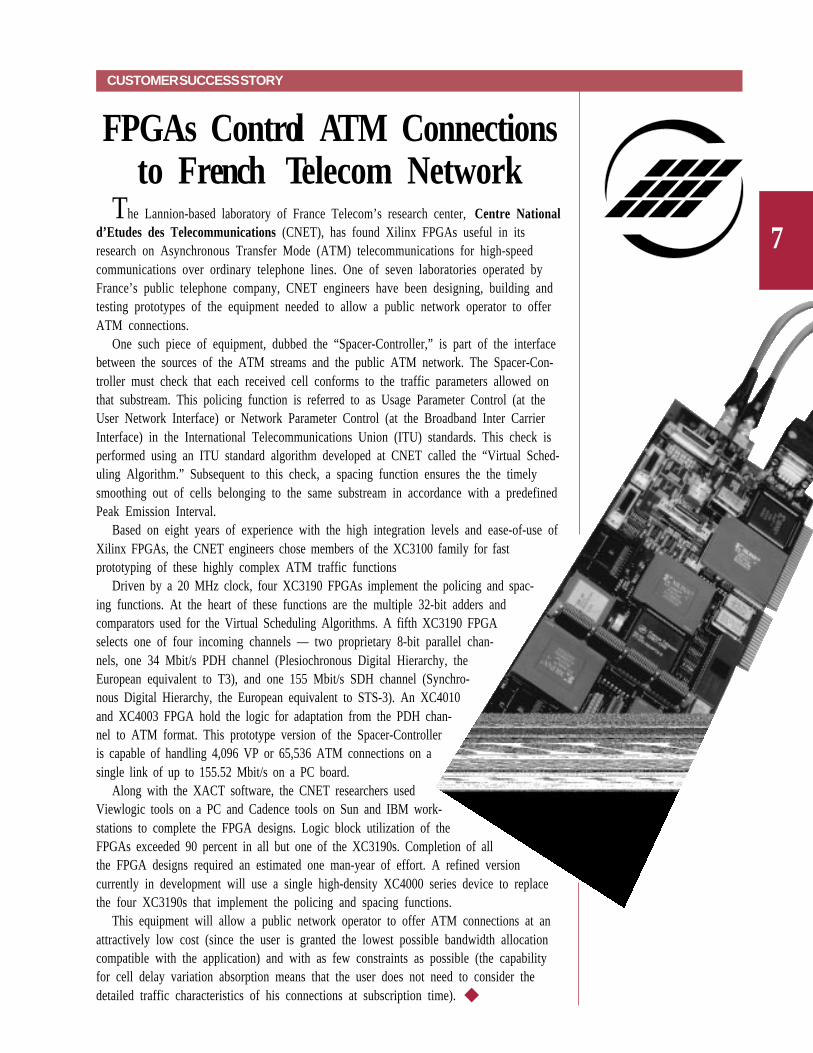
CUSTOMER SUCCESS STORY
FPGAs Control ATM Connectionsto French Telecom Network
The Lannion-based laboratory of France Telecom’s research center, Centre Nationald’Etudes des Telecommunications (CNET), has found Xilinx FPGAs useful in itsresearch on Asynchronous Transfer Mode (ATM) telecommunications for high-speedcommunications over ordinary telephone lines. One of seven laboratories operated byFrance’s public telephone company, CNET engineers have been designing, building andtesting prototypes of the equipment needed to allow a public network operator to offerATM connections.
One such piece of equipment, dubbed the “Spacer-Controller,” is part of the interfacebetween the sources of the ATM streams and the public ATM network. The Spacer-Con-troller must check that each received cell conforms to the traffic parameters allowed onthat substream. This policing function is referred to as Usage Parameter Control (at theUser Network Interface) or Network Parameter Control (at the Broadband Inter CarrierInterface) in the International Telecommunications Union (ITU) standards. This check isperformed using an ITU standard algorithm developed at CNET called the “Virtual Sched-uling Algorithm.” Subsequent to this check, a spacing function ensures the the timelysmoothing out of cells belonging to the same substream in accordance with a predefinedPeak Emission Interval.
Based on eight years of experience with the high integration levels and ease-of-use ofXilinx FPGAs, the CNET engineers chose members of the XC3100 family for fastprototyping of these highly complex ATM traffic functions
Driven by a 20 MHz clock, four XC3190 FPGAs implement the policing and spac-ing functions. At the heart of these functions are the multiple 32-bit adders andcomparators used for the Virtual Scheduling Algorithms. A fifth XC3190 FPGAselects one of four incoming channels — two proprietary 8-bit parallel chan-nels, one 34 Mbit/s PDH channel (Plesiochronous Digital Hierarchy, theEuropean equivalent to T3), and one 155 Mbit/s SDH channel (Synchro-nous Digital Hierarchy, the European equivalent to STS-3). An XC4010and XC4003 FPGA hold the logic for adaptation from the PDH chan-nel to ATM format. This prototype version of the Spacer-Controlleris capable of handling 4,096 VP or 65,536 ATM connections on asingle link of up to 155.52 Mbit/s on a PC board.
Along with the XACT software, the CNET researchers usedViewlogic tools on a PC and Cadence tools on Sun and IBM work-stations to complete the FPGA designs. Logic block utilization of theFPGAs exceeded 90 percent in all but one of the XC3190s. Completion of allthe FPGA designs required an estimated one man-year of effort. A refined versioncurrently in development will use a single high-density XC4000 series device to replacethe four XC3190s that implement the policing and spacing functions.
This equipment will allow a public network operator to offer ATM connections at anattractively low cost (since the user is granted the lowest possible bandwidth allocationcompatible with the application) and with as few constraints as possible (the capabilityfor cell delay variation absorption means that the user does not need to consider thedetailed traffic characteristics of his connections at subscription time).
8
Learn about the newest Xilinx products and services through our extensive library ofproduct literature. The most recent pieces are listed below. To order or to obtain a com-plete list of all available literature, please contact your local Xilinx sales representative.
Strong Revenue Growth ContinuesXilinx sales revenues for the second fiscal quarter
(ending September 30, 1995) rose to a record $141.2million, an increase of 12 percent from the previousquarter and 78 percent from the same quarter oneyear ago.
The revenue increase resulted from growth inseveral product families. The XC4000 family contin-ued its strong pace, accounting for 43 percent of totalrevenues and 50 percent of incoming orders. EPLDrevenues grew 80 percent to more than $3 million.The new XC5200 family generated its first milliondollars in sales revenue.
Geographically, revenues from North America re-mained strong, increasing 15 percent over the previousquarter. The European market was surprisingly robust fora summer quarter, growing 33 percent from the previousquarter and contributing 22 percent of total revenues.
Looking ahead to the next six months, CEO BernieVonderschmitt stated that, “Our recent bookings momen-tum, strong backlog position, and new product strengthposition Xilinx favorably for continued growth in thesecond half of the year.”
Xilinx stock is traded on the NASDAQ exchangeunder stock symbol XLNX.
FINANCIAL RESULTS
New ProductLiterature
CorporateProduct Overview Brochure Features & Benefits #0010130-05EPLDsXC7336 Data Sheet Technical Data #0010269-01FPGAsUser Access to XC6200 Configuration Memory Application Note #0010264-01Interfacing XC6200 to Microprocessors (TMS320C50) Application Note #0010265-01Interfacing XC6200 to Microprocessors (MC68020) Application Note #0010266-01XC5200 Data Sheet Technical Data #0010267-01XC8100 Data Sheet Technical Data #0010193-04
TITLE DESCRIPTION NUMBER
Design SuperCon 96Jan. 30-Feb. 1Santa Clara, California
1996 ACM/SIGDAFourth InternationalSymposium on FPGAsFeb. 11-13Monterey, California
International IC ConferenceMar. 27-29Shanghai, China
PCI 96Apr. 14-18San Jose, California
DigitronicsApr. 17-18Birmingham, UK
European Designand Test ConferenceMar. 12-14Paris, France
DSPx 96Mar. 11-14San Jose, California
UPCOMING EVENTS
Look for Xilinx technical papers and/or product exhibits at these upcoming industryforums. For further information about any of these conferences, please contact KathleenPizzo (Tel: 408-879-5377 FAX: 408-879-4676).
9
What’s New at WebLINX?• XCELL journal issues 17, 18, and 19• New Technology Licensing and Partnership Program—
Xilinx is always looking for leading-edge hardware and soft-ware technologies, new products, and new services. Here’swhere to input your ideas.
• Product Literature— XC8100 FPGA family press release, product
overview and data sheet— XC6200 FPGA family data sheet— Updated XC4000E FPGA family data sheet— New application notes
• Coming Soon: Keyword Searching — Findwhat you want fast with a search of all XilinxWebLINX HTML and PDF files, as well as otherprogrammable logic sites (distributors, universities,partners, etc.)
Any Suggestions?What new content, service, or searchable web site would you like to see on WebLINX?
Send suggestions to [email protected].
The Xilinx home page athttp://www.xilinx.com
One-Day XACTstep 6.0 Update ClassXilinx now offers a one-day training
class for current users focusing on theXACTstepTM version 6 update. This classprovides the fastest way to make the tran-sition to the new features of XACTstep,including the Windows-based interface,the XACT-FloorplannerTM, and XC5200 andXC4000E FPGA family support. Emphasisis placed on gaining hands-on experiencewith the new graphical tools.
The update does notoverlap with previousseminars. Usersshould have experi-
ence with the currentXACT® 5.x tools to get the
most from the one-dayupdate; the standard three-
day class, which inte-grates software traininginto the overall designflow, is recommended
for new users. In the one-
day update, all the new features will bedescribed in relation to the previousXDM-based environment. Again, there islittle overlap with earlier training; in fact,the update class is best for those whohave attended Xilinx training on the ear-lier tools.
Although most of the Windows-basedtools are only available on the PC, work-station users have access to the newgraphical Floorplanner. Current worksta-tion users can attend the morning part ofthe update session, which covers the newdevices and the Floorplanner.
Classes are scheduled at many of ourexisting training locations. Tuition is $100in North America, but will be waived forthose who attended the three-day trainingsince April, 1995. Contact your localsales office, send e-mail [email protected], orcheck the WebLINX web site fordetails.
10
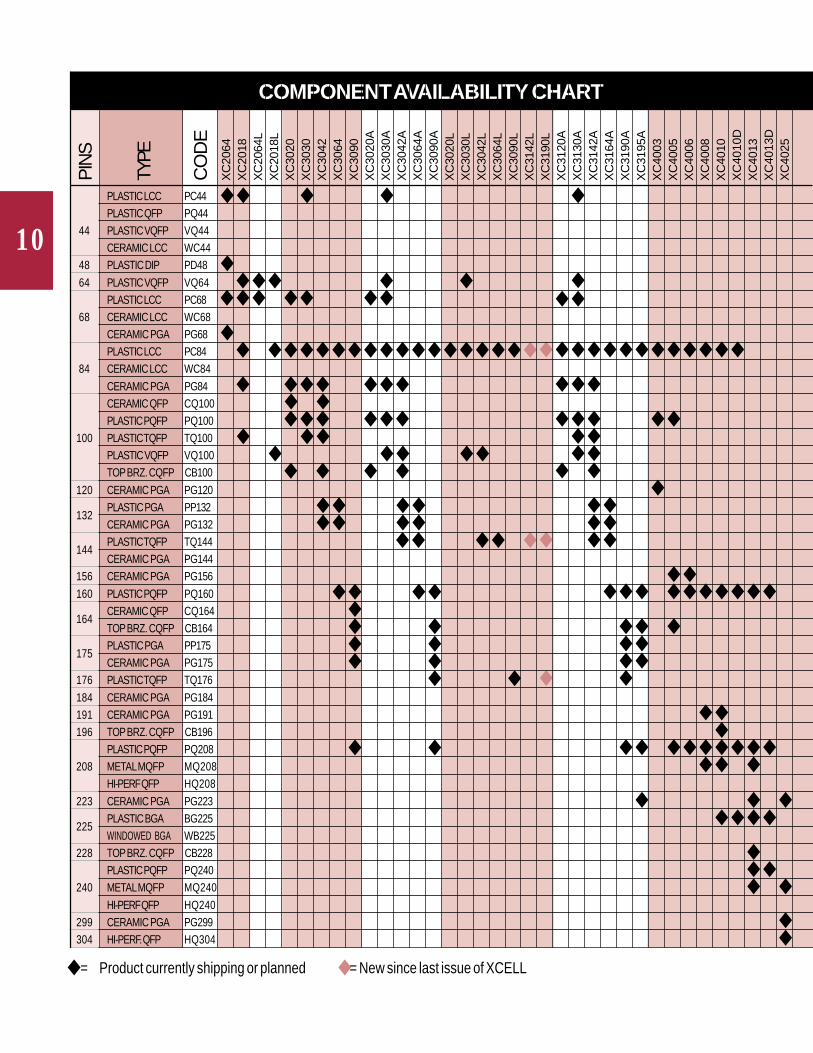
COMPONENT AVAILABILITY CHART
44
48
64
68
84
100
120
132
144
156
160
164
175
176
184191196
208
223
225
228
240
299304
PIN
S
TYPE
CO
DE
XC
2064
XC
2018
XC
2064
LX
C20
18L
XC
3020
XC
3030
XC
3042
XC
3064
XC
3090
XC
3020
AX
C30
30A
XC
3042
AX
C30
64A
XC
3090
AX
C30
20L
XC
3030
LX
C30
42L
XC
3064
LX
C30
90L
XC
3142
LX
C31
90L
XC
3120
AX
C31
30A
XC
3142
AX
C31
64A
XC
3190
AX
C31
95A
XC
4003
XC
4005
XC
4006
XC
4008
XC
4010
XC
4010
DX
C40
13X
C40
13D
XC
4025
PLASTIC LCC PC44PLASTIC QFP PQ44PLASTIC VQFP VQ44CERAMIC LCC WC44PLASTIC DIP PD48
PLASTIC VQFP VQ64PLASTIC LCC PC68CERAMIC LCC WC68CERAMIC PGA PG68PLASTIC LCC PC84CERAMIC LCC WC84
CERAMIC PGA PG84CERAMIC QFP CQ100PLASTIC PQFP PQ100PLASTIC TQFP TQ100PLASTIC VQFP VQ100TOP BRZ. CQFP CB100
CERAMIC PGA PG120PLASTIC PGA PP132CERAMIC PGA PG132PLASTIC TQFP TQ144CERAMIC PGA PG144CERAMIC PGA PG156
PLASTIC PQFP PQ160CERAMIC QFP CQ164TOP BRZ. CQFP CB164PLASTIC PGA PP175CERAMIC PGA PG175PLASTIC TQFP TQ176
CERAMIC PGA PG184CERAMIC PGA PG191TOP BRZ. CQFP CB196PLASTIC PQFP PQ208METAL MQFP MQ208HI-PERF QFP HQ208
CERAMIC PGA PG223PLASTIC BGA BG225WINDOWED BGA WB225TOP BRZ. CQFP CB228PLASTIC PQFP PQ240METAL MQFP MQ240
HI-PERF QFP HQ240CERAMIC PGA PG299HI-PERF. QFP HQ304
= Product currently shipping or planned = New since last issue of XCELL
11
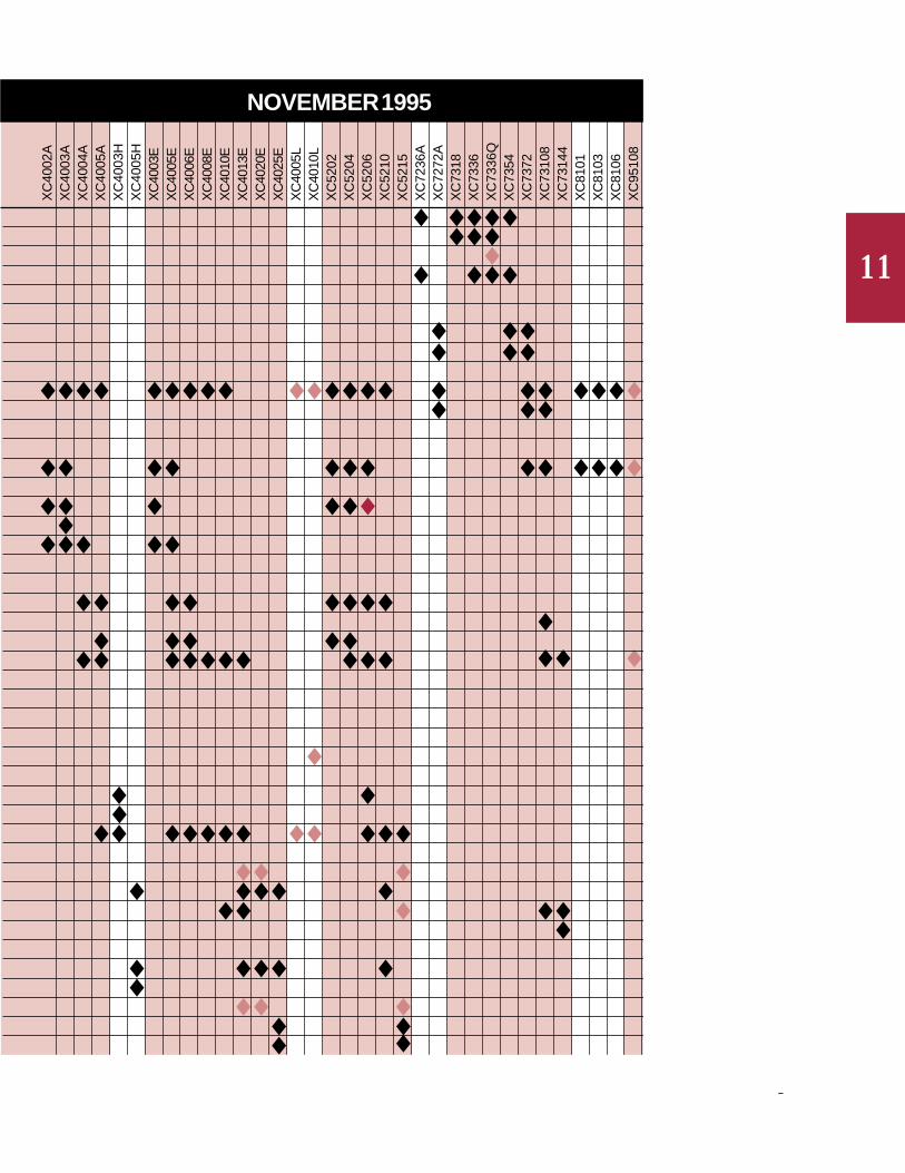
NOVEMBER 1995
XC
4002
AX
C40
03A
XC
4004
AX
C40
05A
XC
4003
HX
C40
05H
XC
4003
EX
C40
05E
XC
4006
EX
C40
08E
XC
4010
EX
C40
13E
XC
4020
EX
C40
25E
XC
4005
LX
C40
10L
XC
5202
XC
5204
XC
5206
XC
5210
XC
5215
XC
7236
AX
C72
72A
XC
7318
XC
7336
XC
7336
QX
C73
54X
C73
72X
C73
108
XC
7314
4X
C81
01X
C81
03X
C81
06X
C95
108
12
2K/3K/4K XC5200 EPLD UNIFIED LIB.COMPANY PRODUCT NAME VERSION FUNCTION DESIGN KIT SUPPORT SUPPORT SUPPORT SUPPORT
Acugen ATGEN 2.60 Automatic Test Generation AALCA interface Sharpeye 2.60 Testability Analysis AALCA interface
ALDEC/Susie-CAD Active-Xilinx 2.0 Schematic Entry/Simulation Included Active-Xlx-State 2.0 Schematic State Editor/ Included
HDL Editor SimulationActive-Xlx-Syn 2.0 Schematic State Editor/ Included
HDL Editor Synthesis Sim.Aptix System Explorer 2.1 System Emulation Axess 2.1
ASIC Explorer 2.3 ASIC Emulation Axess 2.3 4K
Cadence (Valid) Concept 2.0-P7 Schematic Entry Xilinx Front End Q4 Rapidsim 4.2 Simulation Xilinx Front End Q4 Composer 4.3.3 Schematic Entry Xilinx Front End Q4 Verilog 2.2.1 Simulation Xilinx Front End Q4 FPGA Designer 3.3 Synthesis FPGA Synthesis Q4
Capilano DesignWorks 3.1 Schematic Entry/Simulation XD-1
Compass Asic Navigator Schematic Entry Xilinx Design Kit QSim Simulation X-Syn Synthesis
Data I/O ABEL 6.1 Synthesis XEPLD Fitter Synario 2.1 Schematic Entry, Synthe- SYN-LCA
sis and Simulation SYN-XEPLD
Escalade DesignBook Design Entry
Exemplar Logic Galileo 3.1.1 Synthesis Included
Flynn Systems FS-ATG 2.6 Test Vector Generation Xilinx Kit Probe 2.6 Testability Analysis Xilinx Kit CKTSIM 2.6 Logic Analysis Xilinx Kit FS-SIM 2.6 Simulation Xilinx Kit
IBM-EDA Boole-Dozer Synthesis
IK Technology G-DRAW 5.0 Schematic Entry GDL2XNF G-LOG 4.03 Simulation XNF2GDL
Ikos Voyager 2.10 Simulation Xilinx Tool Kit
Incases Theda 2.0 Schematic Entry Xilinx Kit
Intergraph VeriBest Design Capture 14.0 Design Capture Xilinx FPGA Design Kit 3K,4K VeriBest Simulator 14.0 Simulation Xilinx FPGA Design Kit 3K,4K Veribest DMM 14.0 Design Management Xilinx FPGA Design Kit 3K,4K VeriBest Synthesis 14.0 Synthesis Xilinx FPGA Design Kit 3K,4K ACEPlus 12.2 Schematic Entry Xilinx FPGA Design Kit 3K,4K AdvanSIM-1076 12.0 Simulation Xilinx FPGA Design Kit 3K,4K Synovation 12.2 Synthesis Xilinx FPGA Design Kit 3K,4K PLDSyn 12.0 Design entry, Synthesis
ISDATA LOG/iC2 4.2 Synthesis, simulation Xilinx Mapper LOG/iC Classic 4.2 Synthesis LCA-PP
IST ASYL+ 3.2.1 Synthesis, Partitioning XNF interface
ITS XNF2LAS 1a Lasar model gen. XNF2LAS
Logic Modeling Smart Model Simulation Models In Smart Model Library (Synopsys Division) LM1200 Hardware Modeler Xilinx Logic Module
Logical Devices CUPL 4.5 Synthesis Xilinx Fitter
Mentor Graphics QuickSim II A.x_F Simulation Call Xilinx Design Architect A.x_F Schematic Entry Call Xilinx Autologic A.x_F Synthesis Xilinx Synthesis Library
MINC PLDesigner-XL 3.3 Synthesis Xilinx Design Module
Minelec Ulticap 1.32 Schematic Entry Xilinx Interface 2K,3KOrCAD SDT 386+ 1.2 Schematic Entry Call Xilinx XACT6
Capture 6.1 Schematic Entry Call Xilinx XACT6 XACT6 XACT6 XACT6VST 386+ 1.2 Simulation Call Xilinx Simulate 6.0 Simulation Call XilinxPLD 386+ 2.0 Synthesis Call OrCAD
Protel Advanced Schematic 2.2 Schematic Entry Xilinx interface
Quad Design Motive 4.3 Timing Analysis XNF2MTV
Simucad Silos III 95.100 Simulation Included
Sophia Systems Vanguard 5.31 Schematic Entry Xilinx I/F Kit
Synopsys FPGA Compiler 3.3 Synthesis Call Xilinx 3K,4K Design Compiler 3.3 Synthesis Call Xilinx VSS 3.3 Simulation Call Xilinx
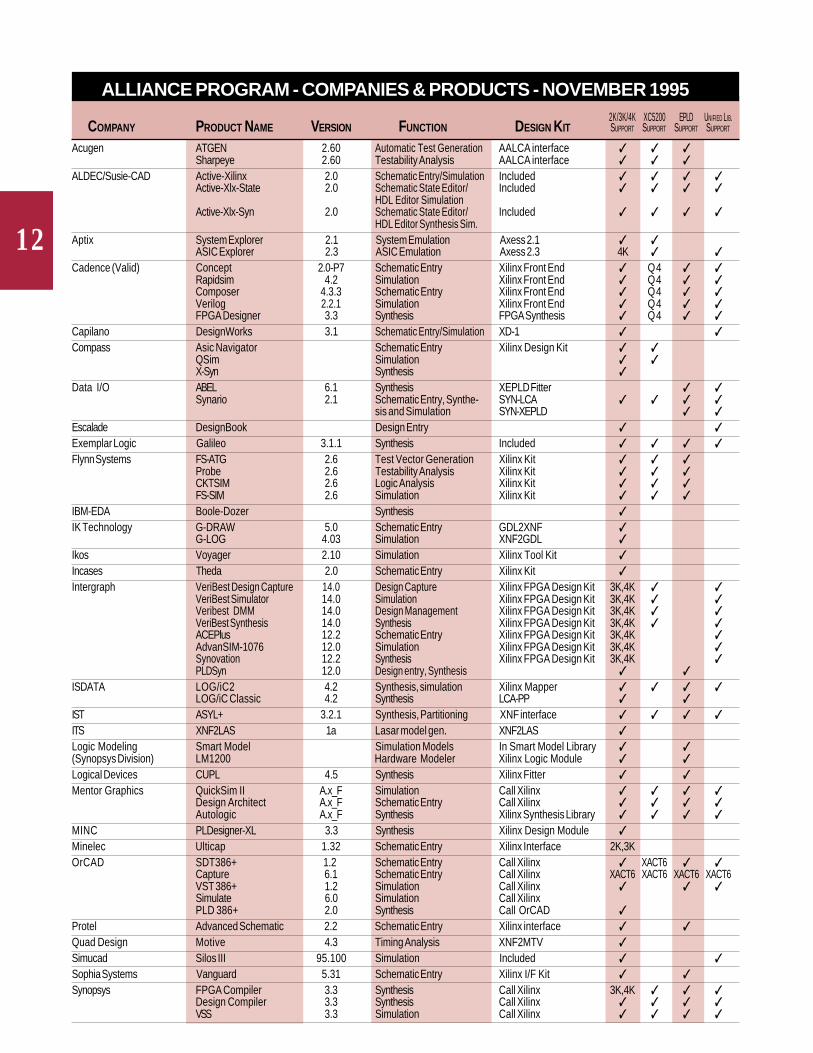
ALLIANCE PROGRAM - COMPANIES & PRODUCTS - NOVEMBER 1995
13
2K/3K/4K XC5200 EPLD UNIFIED LIB.COMPANY PRODUCT NAME VERSION FUNCTION DESIGN KIT SUPPORT SUPPORT SUPPORT SUPPORT
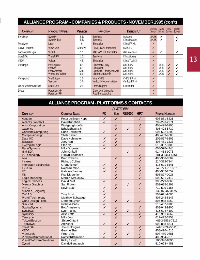
ALLIANCE PROGRAM - COMPANIES & PRODUCTS - NOVEMBER 1995 (con’t)
Synplicity Synplify 2.5c Synthesis Included 3K,4K Synplify-Lite 2.5c Synthesis Xilinx Mapper 3K,4K
Teradyne Lasar 6 Simulation Xilinx I/F Kit
Tokyo Electron ViewCAD 5.0502a FLDL to XNF translator XNFGEN
Topdown Design V-BAK 1.1 XNF to VHDL translator XNF interface
transEDA TransPRO 1.2 Synthesis Xilinx Library
VEDA Vulcan 4.5 Simulation Xilinx Tool Kit
Viewlogic PROCapture 6.1 Schematic Entry Call Xilinx XACT6 PROSim 6.1 Simulation Call Xilinx XACT6 PROSynthesis 5.02 Synthesis, Timing Analysis Call Xilinx XACT6 WorkView Office 5.5 Schem/Sim/Synth Call Xilinx XACT6
Viewpoint VitalBridge 1.0 Vital VHDL VHDL I/F kit VeriLink 1.0 Verilog lib. back-annotation Verilog I/F kit
Visual Software Solutions StateCAD 2.4 State diagram Xilinx fitter
Zycad Paradigm XP Gate-level simulation Paradigm RP Rapid prototyping
ALLIANCE PROGRAM - PLATFORMS & CONTACTSPLATFORM
COMPANY CONTACT NAME PC SUN RS6000 HP7 PHONE NUMBER
Acugen Peter de Bruyn Kops 603-881-8821Aldec/Susie-CAD David Rinehart 702-293-2271Aptix Corporation Wolfgang Hoeflich 408-428-6200Cadence Itzhak Shapira Jr. 408-428-5739Capilano Computing Chris Dewhurst 604-522-6200Compass Design Shahid Khan 408-433-4880Data I/O Dave Kohlmeier 206-867-6802Escalade Jerry Rau 408-481-1336Exemplar Logic Stan Ng 510-337-3700Flynn Systems Mike Jingozian 603-598-4444IBM-EDA John Orfitelli 914-433-9073IK Technology Hiroyuki Kataoka +81-3-3464-5551Ikos Brad Roberts 408-366-8509Incases Richard Collins 214-373-7344Intergraph Electronics Greg Akimoff 415-691-6541ISDATA Ralph Remme +49-721-751087IST Gabriele Saucier 408-982-2557ITS Frank Meunier 508-897-0028Logic Modeling Marnie McCollow 503-531-2412Logical Devices David Mot 303-279-6868Mentor Graphics Sam Picken 503-685-1298MINC Kevin Bush 719-590-1155Minelec (Belgium) +32-02-4603175OrCAD Troy Scott 503-671-9500Protel Technology Matthew Schwaiger 408-243-8143Quad Design Tech. Dermott Lynch 805-988-8250Simucad Richard Jones 510-487-9700Sophia Systems Bob Armstrong 408-943-9300Synopsys Lynn Fiance 415-694-4102Synplicity Alisa Yaffa 415-961-4962Teradyne Mike Jew 617-422-3753Tokyo Electron Shige Ohtani +81-3-5561-7212TopDown Art Pisani 603-888-8811transEDA James Douglas +44-1703-255118VEDA George Sher 408-496-4516ViewLogic Preet Virk 508-480-0881Viewpoint International Ramesh Bhimarao 408-954-7370Visual Software Solutions Ricky Escoto 305-346-8890Zycad David Allenbaugh 510-623-4451
14
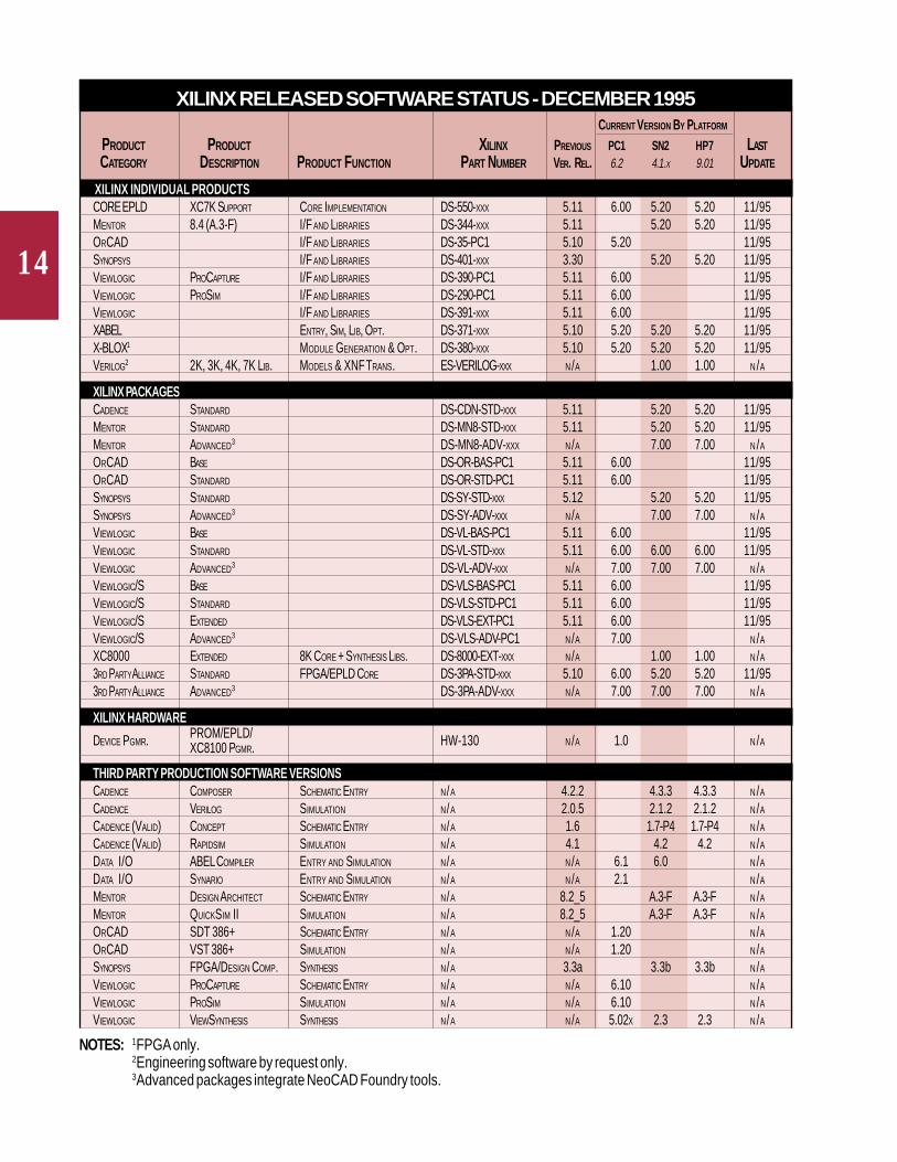
XILINX RELEASED SOFTWARE STATUS - DECEMBER 1995CURRENT VERSION BY PLATFORM
PRODUCT PRODUCT XILINX PREVIOUS PC1 SN2 HP7 LASTCATEGORY DESCRIPTION PRODUCT FUNCTION PART NUMBER VER. REL. 6.2 4.1.X 9.01 UPDATE
XILINX INDIVIDUAL PRODUCTSCORE EPLD XC7K SUPPORT CORE IMPLEMENTATION DS-550-XXX 5.11 6.00 5.20 5.20 11/95MENTOR 8.4 (A.3-F) I/F AND LIBRARIES DS-344-XXX 5.11 5.20 5.20 11/95ORCAD I/F AND LIBRARIES DS-35-PC1 5.10 5.20 11/95SYNOPSYS I/F AND LIBRARIES DS-401-XXX 3.30 5.20 5.20 11/95VIEWLOGIC PROCAPTURE I/F AND LIBRARIES DS-390-PC1 5.11 6.00 11/95VIEWLOGIC PROSIM I/F AND LIBRARIES DS-290-PC1 5.11 6.00 11/95VIEWLOGIC I/F AND LIBRARIES DS-391-XXX 5.11 6.00 11/95XABEL ENTRY, SIM, LIB, OPT. DS-371-XXX 5.10 5.20 5.20 5.20 11/95X-BLOX1 MODULE GENERATION & OPT. DS-380-XXX 5.10 5.20 5.20 5.20 11/95VERILOG2 2K, 3K, 4K, 7K LIB. MODELS & XNF TRANS. ES-VERILOG-XXX N/A 1.00 1.00 N/A
XILINX PACKAGESCADENCE STANDARD DS-CDN-STD-XXX 5.11 5.20 5.20 11/95MENTOR STANDARD DS-MN8-STD-XXX 5.11 5.20 5.20 11/95MENTOR ADVANCED3 DS-MN8-ADV-XXX N/A 7.00 7.00 N/A
ORCAD BASE DS-OR-BAS-PC1 5.11 6.00 11/95ORCAD STANDARD DS-OR-STD-PC1 5.11 6.00 11/95SYNOPSYS STANDARD DS-SY-STD-XXX 5.12 5.20 5.20 11/95SYNOPSYS ADVANCED3 DS-SY-ADV-XXX N/A 7.00 7.00 N/A
VIEWLOGIC BASE DS-VL-BAS-PC1 5.11 6.00 11/95VIEWLOGIC STANDARD DS-VL-STD-XXX 5.11 6.00 6.00 6.00 11/95VIEWLOGIC ADVANCED3 DS-VL-ADV-XXX N/A 7.00 7.00 7.00 N/A
VIEWLOGIC/S BASE DS-VLS-BAS-PC1 5.11 6.00 11/95VIEWLOGIC/S STANDARD DS-VLS-STD-PC1 5.11 6.00 11/95VIEWLOGIC/S EXTENDED DS-VLS-EXT-PC1 5.11 6.00 11/95VIEWLOGIC/S ADVANCED3 DS-VLS-ADV-PC1 N/A 7.00 N/A
XC8000 EXTENDED 8K CORE + SYNTHESIS LIBS. DS-8000-EXT-XXX N/A 1.00 1.00 N/A
3RD PARTY ALLIANCE STANDARD FPGA/EPLD CORE DS-3PA-STD-XXX 5.10 6.00 5.20 5.20 11/953RD PARTY ALLIANCE ADVANCED3 DS-3PA-ADV-XXX N/A 7.00 7.00 7.00 N/A
XILINX HARDWARE
DEVICE PGMR. PROM/EPLD/XC8100 PGMR. HW-130 N/A 1.0 N/A
THIRD PARTY PRODUCTION SOFTWARE VERSIONSCADENCE COMPOSER SCHEMATIC ENTRY N/A 4.2.2 4.3.3 4.3.3 N/A
CADENCE VERILOG SIMULATION N/A 2.0.5 2.1.2 2.1.2 N/A
CADENCE (VALID) CONCEPT SCHEMATIC ENTRY N/A 1.6 1.7-P4 1.7-P4 N/A
CADENCE (VALID) RAPIDSIM SIMULATION N/A 4.1 4.2 4.2 N/A
DATA I/O ABEL COMPILER ENTRY AND SIMULATION N/A N /A 6.1 6.0 N/A
DATA I/O SYNARIO ENTRY AND SIMULATION N/A N /A 2.1 N/A
MENTOR DESIGN ARCHITECT SCHEMATIC ENTRY N/A 8.2_5 A.3-F A.3-F N/A
MENTOR QUICKSIM II SIMULATION N/A 8.2_5 A.3-F A.3-F N/A
ORCAD SDT 386+ SCHEMATIC ENTRY N/A N /A 1.20 N/A
ORCAD VST 386+ SIMULATION N/A N /A 1.20 N/A
SYNOPSYS FPGA/DESIGN COMP. SYNTHESIS N/A 3.3a 3.3b 3.3b N/A
VIEWLOGIC PROCAPTURE SCHEMATIC ENTRY N/A N /A 6.10 N/A
VIEWLOGIC PROSIM SIMULATION N/A N /A 6.10 N/A
VIEWLOGIC VIEWSYNTHESIS SYNTHESIS N/A N /A 5.02X 2.3 2.3 N/A
NOTES: 1FPGA only.2Engineering software by request only.3Advanced packages integrate NeoCAD Foundry tools.
15
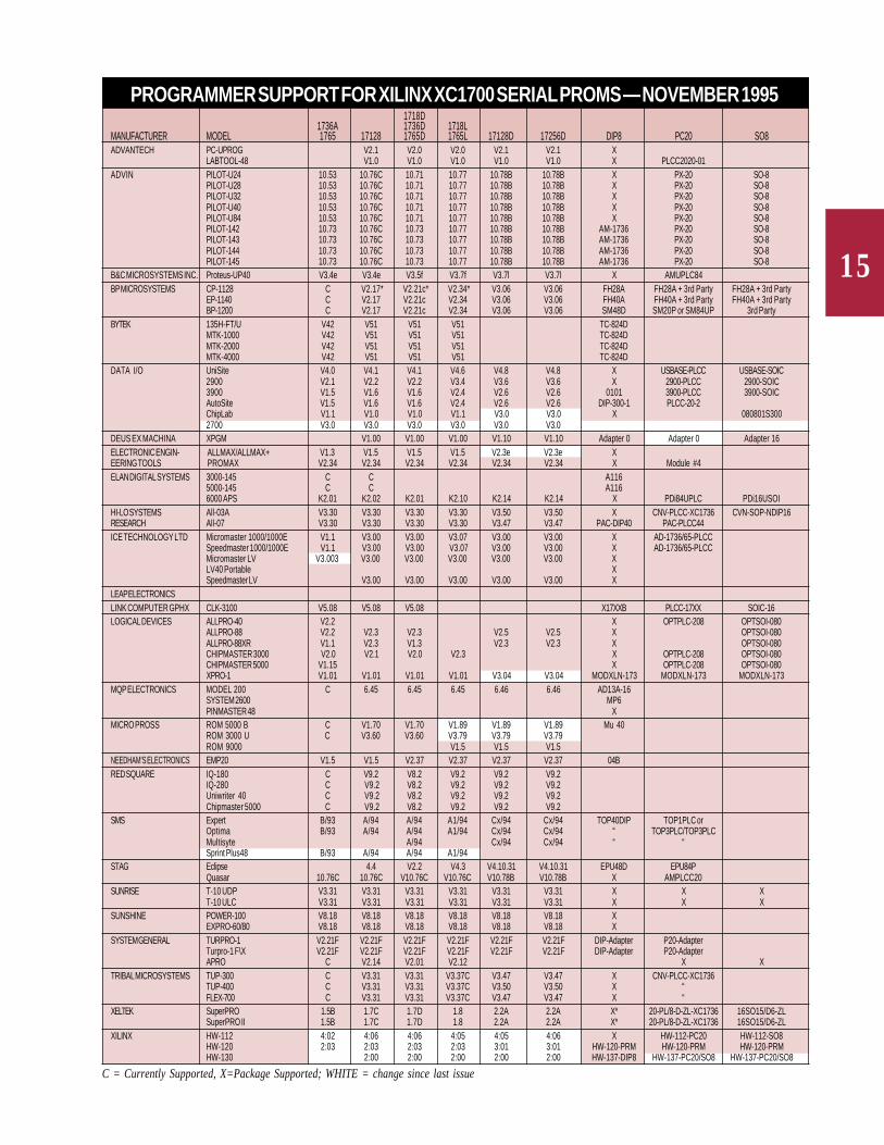
PROGRAMMER SUPPORT FOR XILINX XC1700 SERIAL PROMS — NOVEMBER 19951718D
1736A 1736D 1718LMANUFACTURER MODEL 1765 17128 1765D 1765L 17128D 17256D DIP8 PC20 SO8ADVANTECH PC-UPROG V2.1 V2.0 V2.0 V2.1 V2.1 X
LABTOOL-48 V1.0 V1.0 V1.0 V1.0 V1.0 X PLCC2020-01ADVIN PILOT-U24 10.53 10.76C 10.71 10.77 10.78B 10.78B X PX-20 SO-8
PILOT-U28 10.53 10.76C 10.71 10.77 10.78B 10.78B X PX-20 SO-8PILOT-U32 10.53 10.76C 10.71 10.77 10.78B 10.78B X PX-20 SO-8PILOT-U40 10.53 10.76C 10.71 10.77 10.78B 10.78B X PX-20 SO-8PILOT-U84 10.53 10.76C 10.71 10.77 10.78B 10.78B X PX-20 SO-8PILOT-142 10.73 10.76C 10.73 10.77 10.78B 10.78B AM-1736 PX-20 SO-8PILOT-143 10.73 10.76C 10.73 10.77 10.78B 10.78B AM-1736 PX-20 SO-8PILOT-144 10.73 10.76C 10.73 10.77 10.78B 10.78B AM-1736 PX-20 SO-8PILOT-145 10.73 10.76C 10.73 10.77 10.78B 10.78B AM-1736 PX-20 SO-8
B&C MICROSYSTEMS INC. Proteus-UP40 V3.4e V3.4e V3.5f V3.7f V3.7l V3.7l X AMUPLC84BP MICROSYSTEMS CP-1128 C V2.17* V2.21c* V2.34* V3.06 V3.06 FH28A FH28A + 3rd Party FH28A + 3rd Party
EP-1140 C V2.17 V2.21c V2.34 V3.06 V3.06 FH40A FH40A + 3rd Party FH40A + 3rd PartyBP-1200 C V2.17 V2.21c V2.34 V3.06 V3.06 SM48D SM20P or SM84UP 3rd Party
BYTEK 135H-FT/U V42 V51 V51 V51 TC-824DMTK-1000 V42 V51 V51 V51 TC-824DMTK-2000 V42 V51 V51 V51 TC-824DMTK-4000 V42 V51 V51 V51 TC-824D
DATA I/O UniSite V4.0 V4.1 V4.1 V4.6 V4.8 V4.8 X USBASE-PLCC USBASE-SOIC2900 V2.1 V2.2 V2.2 V3.4 V3.6 V3.6 X 2900-PLCC 2900-SOIC3900 V1.5 V1.6 V1.6 V2.4 V2.6 V2.6 0101 3900-PLCC 3900-SOICAutoSite V1.5 V1.6 V1.6 V2.4 V2.6 V2.6 DIP-300-1 PLCC-20-2ChipLab V1.1 V1.0 V1.0 V1.1 V3.0 V3.0 X 080801S3002700 V3.0 V3.0 V3.0 V3.0 V3.0 V3.0
DEUS EX MACHINA XPGM V1.00 V1.00 V1.00 V1.10 V1.10 Adapter 0 Adapter 0 Adapter 16ELECTRONIC ENGIN- ALLMAX/ALLMAX+ V1.3 V1.5 V1.5 V1.5 V2.3e V2.3e XEERING TOOLS PROMAX V2.34 V2.34 V2.34 V2.34 V2.34 V2.34 X Module #4ELAN DIGITAL SYSTEMS 3000-145 C C A116
5000-145 C C A1166000 APS K2.01 K2.02 K2.01 K2.10 K2.14 K2.14 X PDi84UPLC PDi16USOI
HI-LO SYSTEMS All-03A V3.30 V3.30 V3.30 V3.30 V3.50 V3.50 X CNV-PLCC-XC1736 CVN-SOP-NDIP16RESEARCH All-07 V3.30 V3.30 V3.30 V3.30 V3.47 V3.47 PAC-DIP40 PAC-PLCC44ICE TECHNOLOGY LTD Micromaster 1000/1000E V1.1 V3.00 V3.00 V3.07 V3.00 V3.00 X AD-1736/65-PLCC
Speedmaster 1000/1000E V1.1 V3.00 V3.00 V3.07 V3.00 V3.00 X AD-1736/65-PLCCMicromaster LV V3.003 V3.00 V3.00 V3.00 V3.00 V3.00 XLV40 Portable XSpeedmaster LV V3.00 V3.00 V3.00 V3.00 V3.00 X
LEAP ELECTRONICSLINK COMPUTER GPHX CLK-3100 V5.08 V5.08 V5.08 X17XXB PLCC-17XX SOIC-16LOGICAL DEVICES ALLPRO-40 V2.2 X OPTPLC-208 OPTSOI-080
ALLPRO-88 V2.2 V2.3 V2.3 V2.5 V2.5 X OPTSOI-080ALLPRO-88XR V1.1 V2.3 V1.3 V2.3 V2.3 X OPTSOI-080CHIPMASTER 3000 V2.0 V2.1 V2.0 V2.3 X OPTPLC-208 OPTSOI-080CHIPMASTER 5000 V1.15 X OPTPLC-208 OPTSOI-080XPRO-1 V1.01 V1.01 V1.01 V1.01 V3.04 V3.04 MODXLN-173 MODXLN-173 MODXLN-173
MQP ELECTRONICS MODEL 200 C 6.45 6.45 6.45 6.46 6.46 AD13A-16SYSTEM 2600 MP6PINMASTER 48 X
MICRO PROSS ROM 5000 B C V1.70 V1.70 V1.89 V1.89 V1.89 Mu 40ROM 3000 U C V3.60 V3.60 V3.79 V3.79 V3.79ROM 9000 V1.5 V1.5 V1.5
NEEDHAM’S ELECTRONICS EMP20 V1.5 V1.5 V2.37 V2.37 V2.37 V2.37 04BRED SQUARE IQ-180 C V9.2 V8.2 V9.2 V9.2 V9.2
IQ-280 C V9.2 V8.2 V9.2 V9.2 V9.2Uniwriter 40 C V9.2 V8.2 V9.2 V9.2 V9.2Chipmaster 5000 C V9.2 V8.2 V9.2 V9.2 V9.2
SMS Expert B/93 A/94 A/94 A1/94 Cx/94 Cx/94 TOP40DIP TOP1PLC orOptima B/93 A/94 A/94 A1/94 Cx/94 Cx/94 “ TOP3PLC/TOP3PLCMultisyte A/94 Cx/94 Cx/94 “ “Sprint Plus48 B/93 A/94 A/94 A1/94
STAG Eclipse 4.4 V2.2 V4.3 V4.10.31 V4.10.31 EPU48D EPU84PQuasar 10.76C 10.76C V10.76C V10.76C V10.78B V10.78B X AMPLCC20
SUNRISE T-10 UDP V3.31 V3.31 V3.31 V3.31 V3.31 V3.31 X X XT-10 ULC V3.31 V3.31 V3.31 V3.31 V3.31 V3.31 X X X
SUNSHINE POWER-100 V8.18 V8.18 V8.18 V8.18 V8.18 V8.18 XEXPRO-60/80 V8.18 V8.18 V8.18 V8.18 V8.18 V8.18 X
SYSTEM GENERAL TURPRO-1 V2.21F V2.21F V2.21F V2.21F V2.21F V2.21F DIP-Adapter P20-AdapterTurpro-1 F\X V2.21F V2.21F V2.21F V2.21F V2.21F V2.21F DIP-Adapter P20-AdapterAPRO C V2.14 V2.01 V2.12 X X
TRIBAL MICROSYSTEMS TUP-300 C V3.31 V3.31 V3.37C V3.47 V3.47 X CNV-PLCC-XC1736TUP-400 C V3.31 V3.31 V3.37C V3.50 V3.50 X “FLEX-700 C V3.31 V3.31 V3.37C V3.47 V3.47 X “
XELTEK SuperPRO 1.5B 1.7C 1.7D 1.8 2.2A 2.2A X* 20-PL/8-D-ZL-XC1736 16SO15/D6-ZLSuperPRO II 1.5B 1.7C 1.7D 1.8 2.2A 2.2A X* 20-PL/8-D-ZL-XC1736 16SO15/D6-ZL
XILINX HW-112 4:02 4:06 4:06 4:05 4:05 4:06 X HW-112-PC20 HW-112-SO8HW-120 2:03 2:03 2:03 2:03 3:01 3:01 HW-120-PRM HW-120-PRM HW-120-PRMHW-130 2:00 2:00 2:00 2:00 2:00 HW-137-DIP8 HW-137-PC20/SO8 HW-137-PC20/SO8
C = Currently Supported, X=Package Supported; WHITE = change since last issue
16
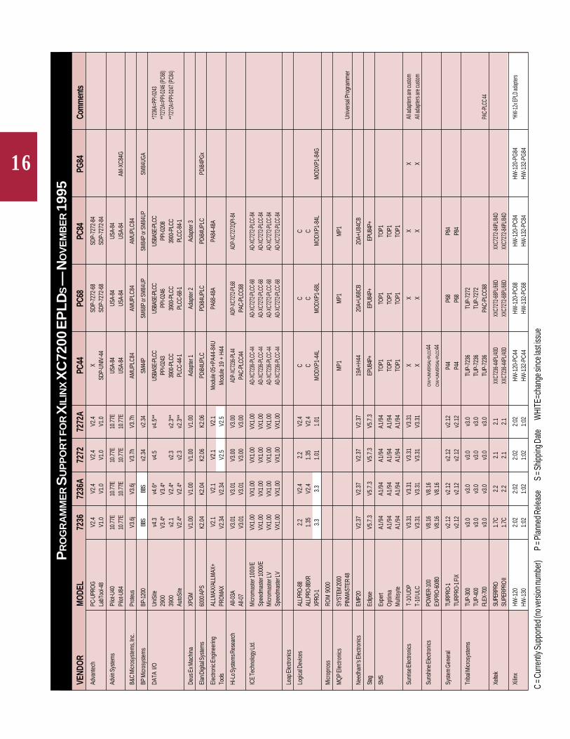
PR
OG
RA
MM
ER S
UP
PO
RT F
OR X
ILIN
X X
C72
00 E
PLD
S —
NO
VE
MB
ER 1
995
VEND
ORM
ODEL
7236
7236
A72
7272
72A
PC44
PC68
PC84
PG84
Comm
ents
Adva
ntec
hPC
-UPR
OGV2
.4V2
.4V2
.4V2
.4X
SDP-
7272
-68
SDP-
7272
-84
LabT
ool-4
8V1
.0V1
.0V1
.0V1
.0SD
P-UN
IV-4
4SD
P-72
72-6
8SD
P-72
72-8
4
Advin
Sys
tem
sPi
lot-U
4010
.77E
10.7
7E10
.77E
10.7
7EUS
A-84
USA-
84US
A-84
Pilo
t-U84
10.7
7E10
.77E
10.7
7E10
.77E
USA-
84US
A-84
USA-
84AM
-XC8
4G
B&C
Micr
osys
tem
s, In
c.Pr
oteu
sV3
.6j
V3.6
jV3
.7h
V3.7
hAM
UPLC
84AM
UPLC
84AM
UPLC
84
BP M
icros
yste
ms
BP-1
200
BBS
BBS
v2.3
4v2
.34
SM44
PSM
68P
or S
M84
UPSM
84P
or S
M84
UPSM
84UG
A
DATA
I/O
UniS
itev4
.3v4
.6*
v4.5
v4.5
**US
BASE
-PLC
CUS
BASE
-PLC
CUS
BASE
-PLC
C*7
236A
=PPI
-0243
2900
V3.4
*V3
.4*
PPI-0
243
PPI-0
246
PPI-0
208
**727
2A=P
PI-02
46 (P
C68)
3900
v2.1
V2.4
*v2
.3v2
.3**
3900
-PLC
C39
00-P
LCC
3900
-PLC
C**7
272A
=PPI
-0247
(PC8
4)Au
toSi
teV2
.4*
V2.4
*v2
.3v2
.3**
PLCC
-44-
1PL
CC-6
8-1
PLCC
-84-
1
Deus
Ex M
achi
naXP
GMV1
.00
V1.0
0V1
.00
V1.0
0Ad
apte
r 1Ad
apte
r 2Ad
apte
r 3
Elan
Digi
tal S
yste
ms
6000
APS
K2.0
4K2
.04
K2.0
6K2
.06
PDi84
UPLC
PDi84
UPLC
PDi84
UPLC
PDi84
PGx
Elec
troni
c Eng
inee
ring
ALLM
AX/A
LLM
AX+
V2.1
V2.1
V2.1
V2.1
Mod
ule
05+P
A44-
84U
PA68
-48A
PA84
-48A
Tools
PROM
AXV2
.34
V2.3
4V2
.5V2
.5M
odul
e 19
+ H
44
Hi-L
o Sys
tem
s Res
earc
hAl
l-03A
V3.0
1V3
.01
V3.0
0V3
.00
ADP-
XC72
36-P
L44
ADP-
XC72
72-P
L68
ADP-
XC72
72QP
I-84
All-0
7V3
.01
V3.0
1V3
.00
V3.0
0PA
C-PL
CC44
PAC-
PLCC
68
ICE
Tech
nolo
gy Lt
d.M
icrom
aste
r 100
0/E
VX1.
00VX
1.00
VX1.
00VX
1.00
AD-X
C723
6-PLC
C-44
AD-X
C727
2-PLC
C-68
AD-X
C727
2-PLC
C-84
Spee
dmas
ter 1
000/
EVX
1.00
VX1.
00VX
1.00
VX1.
00AD
-XC7
236-P
LCC-
44AD
-XC7
272-P
LCC-
68AD
-XC7
272-P
LCC-
84M
icrom
aste
r LV
VX1.
00VX
1.00
VX1.
00VX
1.00
AD-X
C723
6-PLC
C-44
AD-X
C727
2-PLC
C-68
AD-X
C727
2-PLC
C-84
Spee
dmas
ter L
VVX
1.00
VX1.
00VX
1.00
VX1.
00AD
-XC7
236-P
LCC-
44AD
-XC7
272-P
LCC-
68AD
-XC7
272-P
LCC-
84
Leap
Ele
ctro
nics
Logi
cal D
evice
sAL
LPRO
-88
2.2
V2.4
2.2
V2.4
CC
CAL
LPRO
-88X
R1.
35V2
.41.
35V2
.4C
CC
XPRO
-13.
33.
31.
011.
01M
ODX
P1-4
4LM
ODX
P1-6
8LM
ODX
P1-8
4LM
ODX
P1-8
4G
Micr
opro
ssRO
M 9
000
MQ
P El
ectro
nics
SYST
EM 20
00M
P1M
P1M
P1PI
NMAS
TER
48Un
ivers
al P
rogr
amm
er
Need
ham
’s El
ectro
nics
EMP2
0V2
.37
V2.3
7V2
.37
V2.3
719
A+H4
420
A+U6
8CB
20A+
U84C
B
Stag
Eclip
seV5
.7.3
V5.7
.3V5
.7.3
V5.7
.3EP
U84P
+EP
U84P
+EP
U84P
+
SMS
Expe
rtA1
/94
A1/9
4A1
/94
A1/9
4TO
P1TO
P1TO
P1O
ptim
aA1
/94
A1/9
4A1
/94
A1/9
4TO
P1TO
P1TO
P1M
ultis
yte
A1/9
4A1
/94
A1/9
4A1
/94
TOP1
TOP1
TOP1
Sunr
ise E
lect
roni
csT-
10 U
DPV3
.31
V3.3
1V3
.31
V3.3
1X
XX
XAl
l ada
pters
are c
ustom
T-10
ULC
V3.3
1V3
.31
V3.3
1V3
.31
XX
XX
All a
dapte
rs ar
e cus
tom
Suns
hine E
lectro
nics
POW
ER-1
00V8
.16
V8.1
6CN
V-UN
IVER
SAL -P
LCC4
4EX
PRO-
60/8
0V8
.16
V8.1
6CN
V-UN
IVER
SAL -P
LCC4
4
Syste
m G
ener
alTU
RPRO
-1v2
.12
v2.1
2v2
.12
v2.1
2P4
4P6
8P8
4TU
RPRO
-1 F\
Xv2
.12
v2.1
2v2
.12
v2.1
2P4
4P6
8P8
4
Trib
al M
icros
yste
ms
TUP-
300
v3.0
v3.0
v3.0
v3.0
TUP-
7236
TUP-
7272
TUP-
400
v3.0
v3.0
v3.0
v3.0
TUP-
7236
TUP-
7272
FLEX
-700
v3.0
v3.0
v3.0
v3.0
TUP-
7236
PAC-
PLCC
68PA
C-PL
CC 44
Xelte
kSU
PERP
RO1.
7C2.
22.
12.
1XX
C723
6-44P
L/40D
XXC7
272-6
8PL/6
8DXX
C727
2-84P
L/84D
SUPE
RPRO
II1.
7C2.
22.
12.
1XX
C723
6-44P
L/40D
XXC7
272-6
8PL/6
8DXX
C727
2-84P
L/84D
Xilin
xHW
-120
2:02
2:02
2:02
2:02
HW-1
20-P
C44
HW-1
20-P
C68
HW-1
20-P
C84
HW-1
20-P
G84
*HW
-12x E
PLD a
dapte
rsHW
-130
1:02
1:02
1:02
1:02
HW-1
32-P
C44
HW-1
32-P
C68
HW-1
32-P
C84
HW-1
32-P
G84
C = C
urre
ntly
Supp
orte
d (no
vers
ion nu
mbe
r)P
= Plan
ned R
eleas
eS
= Ship
ping D
ate
WHI
TE=c
hang
e sinc
e las
t issu
e

VEND
ORMO
DEL
7318
7336
7336
Q73
5473
7273
108
7314
4PC
44PC
68PC
84PQ
44PQ
100
PG14
4PQ
160
BG22
5
ADVA
NTEC
HPC
-UPR
OGV2
.4V2
.4V2
.4X
SDP-
7354
-68
LabT
ool-4
8V1
.0V1
.0V1
.0V1
.04V1
.04SD
P-UN
IV-4
4SD
P-73
54-6
8X
ADVI
N SYS
TEMS
PILO
T-U4
010
.78N
10.7
8N10
.78N
10.7
8N10
.79
USA-
84US
A-84
USA-
84AM
-XC1
00Q
AM-X
C144
GAM
-XC1
60Q
PILO
T-U8
410
.78B
10.78
B10
.78B
10.78
B10
.79
USA-
84US
A-84
USA-
84AM
-XC1
00Q
AM-X
C144
GAM
-XC1
60Q
B&C M
ICRO
SYST
EMS
Prote
us3.
7k3.
7k3.
7k3.
7kC
CC
BP M
ICRO
SYST
EMS
BP-12
00V3
.01V3
.01V3
.01V3
.07V3
.06A
SM44
PFH
SM84
PX
DATA
I/O
2900
V3.5
V3.5
V3.5
2900
-PLC
C05
2939
00/A
utoS
iteV2
.5V2
.5V2
.5V2
.6V2
.639
00-P
LCC
3900
-PLC
C39
00-P
LCC
0529
0557
0558
PPI-1
101
UniS
iteV4
.7V4
.7V4
.7V4
.8V4
.8US
BASE
-PLC
CUS
BASE
-PLC
CUS
BASE
-PLC
C05
2905
5705
58PP
I-110
1
DEUS
EX M
ACHI
NAXP
GMV1
.00V1
.00V1
.30V1
.00V1
.10V1
.10Ad
apte
r 5Ad
apte
r 6Ad
apte
r 7Ad
apte
r 9(1
3 for
7372
)
ELAN
6000
APS
k2.1
3k2
.13
k2.1
3k2
.13
k2.1
3PD
i84UP
LCPD
i84UP
LCPD
i84UP
LCPD
i044Q
FxPD
i100Q
FxPD
i160Q
Fx
ELEC
TRON
IC EN
GIN-
ALLM
AX/A
LLMA
X+V2
.1V2
.1V2
.1V2
.1Mo
dule 0
4+PA
44-48
UPA
68-4
8B (7
354)
PA84
-48B
EERI
NG TO
OLS
PROM
AXV2
.34V2
.34V2
.34V2
.57Mo
dule
#19 +
H44
PA68
-48C
(737
2)
HI-LO
SYST
EMS
All-0
3AV3
.04V3
.04V3
.04V3
.05V3
.01AD
P-XC7
336-PL
44AD
P-XC7
372-PL
68AD
P-XC7
3108-P
L84RE
SEAR
CHAl
l-07
V3.02
V3.02
V3.02
V3.01
V3.00
PAC-
PLCC
44PA
C-PL
CC68
ICE T
ECHN
OLOG
Y LTD
Micr
omas
ter 1
000/
EVX
1.00
VX1.0
0VX
1.00
VX1.0
0VX
1.00
AD-73
XX-PL
CC-44
AD-73
54-P
LCC-
68AD
-73XX
-PLCC
-44AD
-737
2-PL
CC-6
8
Spee
dmas
ter 10
00/E
VX1.0
0VX
1.00
VX1.0
0VX
1.00
VX1.0
0AD
-73XX
-PLCC
-44AD
-7354
-PLC
C-68
AD-73
XX-PL
CC-44
AD-7
372-
PLCC
-68
Micr
omas
ter L
VVX
1.00
VX1.0
0VX
1.00
VX1.0
0VX
1.00
AD-73
XX-PL
CC-44
AD-7
354-
PLCC
-68
AD-73
XX-PL
CC-44
AD-7
372-
PLCC
-68
Spee
dmas
ter LV
VX1.0
0VX
1.00
VX1.0
0VX
1.00
VX1.0
0AD
-73XX
-PLCC
-44AD
-735
4-PL
CC-6
8AD
-73XX
-PLCC
-44AD
-737
2-PL
CC-6
8
LEAP
ELEC
TRON
ICS
LOGI
CAL D
EVIC
ESAL
LPRO
-88V2
.5V2
.5V2
.5V2
.5V2
.5C
CC
ALLP
RO-88
XRV2
.5V2
.5V2
.5V2
.5V2
.5C
CC
XPRO
-13.3
3.31.0
11.0
11.0
1M
ODXP
1-54
44L
MOD
XP1-
5468
LM
ODXP
1-10
8LMO
DXP1
-160Q
MODX
P1-10
8B
MICR
OPRO
SSRO
M 90
00
MQP E
LECT
RONI
CSSY
STEM
2000
MP1
MP1
MP1
PINM
ASTE
R 48
NEED
HAM'
S ELE
CTRO
NICS
EMP2
0V2
.37V2
.37V2
.37V2
.37V2
.3719
B +
H44
20A
+ U6
8CA
20A
+ U8
4CA
SMS
EXPE
RTC/
94C/
94C/
94TO
P1TO
P1TO
P1OP
TIM
AC/
94C/
94C/
94TO
P1TO
P1TO
P1
STAG
ECLIP
SEV4
.10.
31V4
.10.
31V4
.10.
31V4
.10.
31V4
.10.
31
SUNR
ISET-
10 U
DPV3
.31V3
.31V3
.31V3
.31V3
.31X
XX
T-10
ULC
V3.31
V3.31
V3.31
V3.31
V3.31
XX
X
SUNS
HINE
POW
ER-10
0CN
V-UNIV
ERSA
L-PLC
C44
EXPR
O-60
/80CN
V-UNIV
ERSA
L-PLC
C44
SYST
EM GE
NERA
LTU
RPRO
-1V2
.2V2
.2V2
.2V2
.2V2
.2C
TRIB
AL M
ICRO
SYST
EMS
Flex-7
00V3
.02V3
.02V3
.02V3
.01V3
.00PA
C-PL
CC44
PAC-
PLCC
68TU
P-30
0V3
.03V3
.03V3
.03V3
.03TU
P-40
0V3
.03V3
.03V3
.03V3
.03
XELT
EKSU
PERP
RO2.1
2.2A
2.12.2
BXX
C7354
-44PL
/40D
XXC7
354-68
PL/40
DSU
PERP
RO II
2.12.
2A2.1
2.2B
XXC7
354-44
PL/40
DXX
C7354
-68PL
/40D
XILIN
XHW
-120
3:13
3:13
1:00
3:00
1:01
3:01
HW-1
26-P
C44
HW-1
26-P
C68
HW-1
26-P
C84
HW-12
6-PQ4
4HW
-126-P
Q100
HW-12
6-PG1
44HW
-126-P
Q160
HW-12
6-BG2
25HW
-130
1:13
1:18
1:03
1:34
1:08
1:03
1:00
HW-1
33-P
C44
HW-1
33-P
C68
HW-1
33-P
C84
HW-13
3-PQ4
4HW
-133-P
Q100
HW-13
3-PG1
44HW
-133-P
Q160
HW-13
3-BG2
25
PR
OG
RA
MM
ER S
UP
PO
RT F
OR X
ILIN
X X
C73
00 E
PLD
S —
NO
VE
MB
ER 1
995
17
C = C
urre
ntly
Supp
orte
d (no
vers
ion nu
mbe
r)P
= Plan
ned R
eleas
eW
HITE
=cha
nge s
ince l
ast is
sue
18
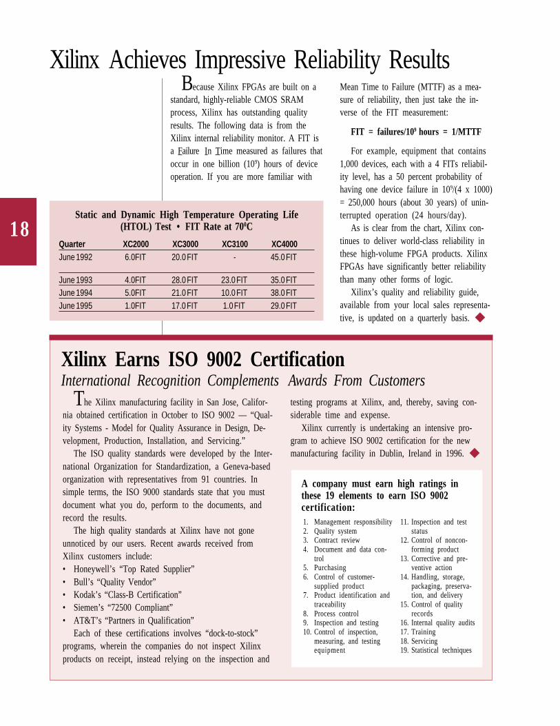
Xilinx Achieves Impressive Reliability ResultsBecause Xilinx FPGAs are built on a
standard, highly-reliable CMOS SRAMprocess, Xilinx has outstanding qualityresults. The following data is from theXilinx internal reliability monitor. A FIT isa Failure In Time measured as failures thatoccur in one billion (109) hours of deviceoperation. If you are more familiar with
Mean Time to Failure (MTTF) as a mea-sure of reliability, then just take the in-verse of the FIT measurement:
FIT = failures/109 hours = 1/MTTF
For example, equipment that contains1,000 devices, each with a 4 FITs reliabil-ity level, has a 50 percent probability ofhaving one device failure in 109/(4 x 1000)= 250,000 hours (about 30 years) of unin-terrupted operation (24 hours/day).
As is clear from the chart, Xilinx con-tinues to deliver world-class reliability inthese high-volume FPGA products. XilinxFPGAs have significantly better reliabilitythan many other forms of logic.
Xilinx’s quality and reliability guide,available from your local sales representa-tive, is updated on a quarterly basis.
Static and Dynamic High Temperature Operating Life(HTOL) Test • FIT Rate at 700C
Quarter XC2000 XC3000 XC3100 XC4000June 1992 6.0 FIT 20.0 FIT - 45.0 FIT
June 1993 4.0 FIT 28.0 FIT 23.0 FIT 35.0 FITJune 1994 5.0 FIT 21.0 FIT 10.0 FIT 38.0 FITJune 1995 1.0 FIT 17.0 FIT 1.0 FIT 29.0 FIT
Xilinx Earns ISO 9002 CertificationInternational Recognition Complements Awards From Customers
The Xilinx manufacturing facility in San Jose, Califor-nia obtained certification in October to ISO 9002 — “Qual-ity Systems - Model for Quality Assurance in Design, De-velopment, Production, Installation, and Servicing.”
The ISO quality standards were developed by the Inter-national Organization for Standardization, a Geneva-basedorganization with representatives from 91 countries. Insimple terms, the ISO 9000 standards state that you mustdocument what you do, perform to the documents, andrecord the results.
The high quality standards at Xilinx have not goneunnoticed by our users. Recent awards received fromXilinx customers include:• Honeywell’s “Top Rated Supplier”• Bull’s “Quality Vendor”• Kodak’s “Class-B Certification”• Siemen’s “72500 Compliant”• AT&T’s “Partners in Qualification”
Each of these certifications involves “dock-to-stock”programs, wherein the companies do not inspect Xilinxproducts on receipt, instead relying on the inspection and
testing programs at Xilinx, and, thereby, saving con-siderable time and expense.
Xilinx currently is undertaking an intensive pro-gram to achieve ISO 9002 certification for the newmanufacturing facility in Dublin, Ireland in 1996.
A company must earn high ratings inthese 19 elements to earn ISO 9002certification:1. Management responsibility2. Quality system3. Contract review4. Document and data con-
trol5. Purchasing6. Control of customer-
supplied product7. Product identification and
traceability8. Process control9. Inspection and testing10. Control of inspection,
measuring, and testingequipment
11. Inspection and teststatus
12. Control of noncon-forming product
13. Corrective and pre-ventive action
14. Handling, storage,packaging, preserva-tion, and delivery
15. Control of qualityrecords
16. Internal quality audits17. Training18. Servicing19. Statistical techniques
19
R
PRODUCT INFORMATION — COMPONENTS
XC8100 Shines in 6502Processor Benchmark
As reported in the December 1994issue of Electronic Engineering Times,VHDL model vendor VAutomation Inc .has evaluated several different FPGA tech-nologies using a technology-independentVHDL description of the 6502 8-bit micro-processor.
VAutomation’s V6502 synthesizablemodule allows this processor to beintegrated into an ASIC device along withother logic and memory functions.However, their customers often want toprototype the ASIC design prior to com-mitting to silicon, thus providing themotivation to test how this model isimplemented in FPGAs.
The design was compiled with PC-based synthesis tools from ExemplarLogic, using the default constraints. Eachimplementation was then placed androuted using the respective FPGA vendor’stools, again using default settings. TheV6502 proved a difficult model to imple-ment in an FPGA since it is very logicintensive; that is, the model has a highratio of logic gates to flip-flops, largelydue to the large amount of highly-inter-connected logic needed to decode theprocessor’s opcodes.
VAutomation recently benchmarked theXC8106 FPGA using the V6502 model. TheXC8100 architecture is designed to beespecially efficient when using top-down,high-level design methodologies. Since theXC8100 logic cell can be used to imple-ment either logic or register functions, theratio of logic gates to registers in the de-sign has little effect on utilization. As aresult, the design fit into a 6,000-gateXC8106 device, as opposed to requiring10,000-gate or larger devices in other
FPGA technologies (see Table 1). Thedesign uses 90 percent of the cells inthe XC8106.
The VAutomation engineer was able toinstall the XC8100 design tools, learn theiruse, and complete the design within fivedays of receiving the beta site softwarefrom Xilinx. After completing the designand programming the device, the chipwas plugged into an adapter that attached
to the 6502’s socket in an Apple IIc com-puter. The computer was then booted up,and it worked the very first time!
Table 2 shows the production statusof XC8100 devices and the XACTstepSeries 8000 development tools. Pleasecontact your local Xilinx sales representa-tive for further pricing and availabilityinformation.
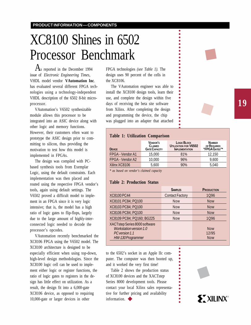
Table 1: Utilization ComparisonVENDOR’S LOGIC BLOCK NUMBERCLAIMED UTILIZATION FOR V6502 OF REQUIRED
DEVICE GATE CAPACITY IMPLEMENTATION “FPGA G ATES”*FPGA - Vendor A1 15,000 81% 12,150FPGA - Vendor A2 10,000 96% 9,600Xilinx XC8106 5,600 90% 5,040* as based on vendor’s claimed capacity
Table 2: Production Status
SAMPLES PRODUCTION
XC8100 PC44 Contact Factory 1Q96XC8101 PC84; PQ100 Now NowXC8103 PC84; PQ100 Now NowXC8106 PC84; PQ100 Now NowXC8109 PC84; PQ160; BG225 Now 1Q96XACTstep Series 8000 software
Workstation version 1.0 NowPC version 1.1 12/95HW-130 Programmer Now
20
Introducing the FastFLASH XC9500 The new XC9500 family is the second
generation of Xilinx CPLDs, developedespecially for system designers who re-quire complete in-system programming,test and manufacturing capability. TheXC9500 family provides a total product lifecycle support solution from initial
prototyping to system integration, manu-facturing and field upgrades. It also offersthe industry’s best pin-locking capability, anecessity for maintaining device pinoutsthroughout the complete product life cycle.
The innovative FastFLASH technologyprovides exceptional in-system program-mable (ISP) capabilities by offering morethan 10,000 program/erase cycles — oneor two orders of magnitude more thanother comparable CPLDs. This high endur-ance level allows the XC9500 devices to beused in applications requiring frequentfield upgrades and reconfigurations.
In addition, the XC9500 family providesboth superior density and performance,with seven devices ranging in density from
800 to 6,400 usable gates, and pin-to-pinpropagation delays as fast as 5 ns.
Product Features• High-performance
— 5 ns pin-to-pin logic delays onall pins
— Maximum external frequency to145 MHz
• Large density range— 36 to 288 macrocells with 800 to
6,400 usable gates• 5 V in-system programmability (ISP)
— Endurance of 10,000 program/erasecycles
— Program/erase over full voltage andtemperature range
• Enhanced pin-locking architecture• Flexible 36V18 Function Block• Extensive IEEE 1149.1 boundary-scan
(JTAG) support• Programmable speed/power options on
individuals macrocells• Slew rate control on individual outputs• User programmable ground pins capa-
bility• Extended pattern security features for
design protection— Read security bit prevents unautho-
rized copying of design— Write security bit protects against
inadvertent user programming/erase• High-drive 24 mA outputs with 3.3 V or
5 V I/O• 100-percent PCI compliant (-10, -7
speed grades)• Advanced 0.6µm CMOS 5 V FastFLASH
technology
Product Life Cycle SupportDuring the prototyping stage, a device
might be reprogrammed hundreds oftimes while soldered on a printed circuitboard (PCB). If the architecture does notsupport locking the device pinout, anexpensive and time-consuming re-layout
21
Family The Industry’s Most Complete Solutionfor In-System Programmable CPLDs.
of the PCB is necessary. The XC9500 fam-ily provides industry-leading pin-lockingcapability for preserving PCB board layoutthroughout the design cycle.
When the entire system is assembled fortest and debug, all important logic statesshould be easily accessible, and internallogic implementations within each CPLDshould be capable of being checked. EachXC9500 device supports the IEEE 1149.1boundary scan specification, includingINTEST and USERCODE instructions usedto access and debug user logic and trackpattern revisions, respectively. In addition,both the superior pin-locking and highendurance features of the XC9500 familyare critical in facilitating design modifica-tions during the debugging process.
Full JTAG SupportThe XC9500 family expands the manu-
facturing process capability with theindustry’s most complete IEEE 1149.1 JTAGsupport. By integrating device program-ming with final board testing, the XC9500technology eliminates the needfor stand-alone mark and pro-gramming steps. Built-in versioncontrol, concurrent programmingof multiple devices and in-systemboard customization all contributeto manufacturing flexibility.
Since the XC9500 family iseasily programmed through theJTAG port, field upgrades to theCPLD’s configuration are possible.The industry’s best pin-lockingarchitecture ensures againstchanges to the PCB layout.
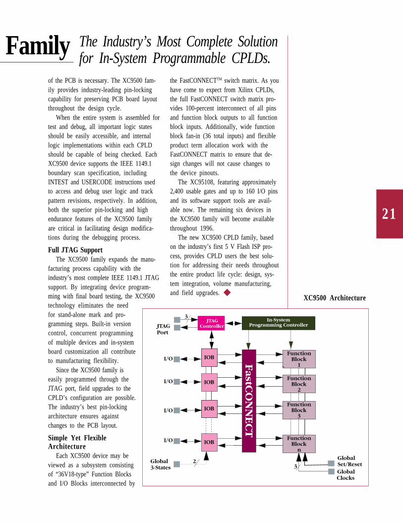
Simple Yet FlexibleArchitecture
Each XC9500 device may beviewed as a subsystem consistingof “36V18-type” Function Blocksand I/O Blocks interconnected by
the FastCONNECTTM switch matrix. As youhave come to expect from Xilinx CPLDs,the full FastCONNECT switch matrix pro-vides 100-percent interconnect of all pinsand function block outputs to all functionblock inputs. Additionally, wide functionblock fan-in (36 total inputs) and flexibleproduct term allocation work with theFastCONNECT matrix to ensure that de-sign changes will not cause changes tothe device pinouts.
The XC95108, featuring approximately2,400 usable gates and up to 160 I/O pinsand its software support tools are avail-able now. The remaining six devices inthe XC9500 family will become availablethroughout 1996.
The new XC9500 CPLD family, basedon the industry’s first 5 V Flash ISP pro-cess, provides CPLD users the best solu-tion for addressing their needs throughoutthe entire product life cycle: design, sys-tem integration, volume manufacturing,and field upgrades.
XC9500 Architecture
22
XC5200 Family Now In Volumeand by delivering architectural innova-tions, Xilinx has dramatically reduced diearea and size. Xilinx now provides theindustry‘s highest value family of FPGAs.
DEVICE USABLE GATES
XC5202 2,200–2,700XC5204 3,900–4,800XC5206 6,000–7,500XC5210 10,000–12,000XC5215 14,000–18,000
With powerful new features such as theVersaRingTM I/O interface, dedicated JTAGlogic for increased testability, and fastcarry logic for high speed arithmetic func-tions, the XC5200 is the optimal solution
All XC5200 family devices and thesupporting XACTstepTM design software arenow in volume production. With fivedevices — ranging from 2,000 to 18,000usable gates — offered in 15 differentpackages, there are now more than 100different device/package/speed combina-tions available to meet the most exactingdesign requirements. Complete footprintcompatibility between all devices in acommon package allows the migration tohigher or lower density devices withoutmodifying the printed circuit board. AllXC5200 devices are also footprint-compat-ible with the XC4000 and XC8100 families.
By optimizing the XC5200 family for a0.6 micron, three-layer-metal SRAM process
XC3100A-09: The World’s Fastest FPGAThe popular XC3100A family has attained a 50 percent boost
in performance from changes in manufacturing process andlayout. The new XC3100A-09 and XC3100A-1 devices weredesigned with an optimized 0.6µ, triple-layer-metal processtechnology.
The XC3100A-09 has 40 percent shorter block delays, 50percent faster chip-to-chip speed and decoding functions, as wellas 100 percent faster interconnect speed compared with theXC3100A-2 device (see Table 1).
Fully PCI compliant, the XC3100A is ideal for high-speedserial-to-parallel conversions, fast ATM switches, video controlfunctions and 3D graphics/imaging. Designs which require high-speed clock distribution can also benefit.
The Software Help area of the Xilinx bulletin board (408-559-9327) contains advance speed files for use with XACTTM designsoftware. The combination of XC3100A silicon and XACTstep-PerformanceTM, Xilinx’s timing-driven placement software, pro-vide a high level of productivity for high-performance designs.
The new XC3100A devices are fully backward compatiblewith earlier XC3100A devices (that is, they may be dropped inwith the same bitstream). See Table 2 for device availability.
Table 1-09 vs. -02 Performance Comparisons
XC3100A-09 XC3100A-2
Combinatorial Delay 1.4 ns 2.2 nsClock to Out (pin-to-pin) 6 ns 7.8 nsSetup (pin-to-pin) 3.5 ns 6.5 nsInterconnect (normalized) 4.4 ns 10 nsState Machine 112 MHz 68 MHzData Path 356 MHz 233 MHzMax Chip-to-Chip 110 MHz 70 MHz
Table 2XC3100A-09 and XC3100A-1 Availability
Device Sampling ProductionXC3120A December 2Q96XC3130A December 2Q96XC3142A Now 2Q96XC3164A December 2Q96XC3190A Now 1Q96XC3195A Now 1Q96
23
Productionfor high density designs not requiring thehigh performance and on-chip RAM of theXC4000 series.
The XC5200 family is completely inte-grated into the powerful XACTstep designtools. All in-warranty users will receiveXC5200 software as part of the XACTstepversion 6 (Windows) and XACTstep 5.2(DOS) production release.
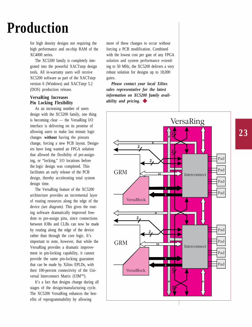
VersaRing IncreasesPin Locking Flexibility
As an increasing number of usersdesign with the XC5200 family, one thingis becoming clear — the VersaRing I/Ointerface is delivering on its promise ofallowing users to make last minute logicchanges without having the pinoutschange, forcing a new PCB layout. Design-ers have long wanted an FPGA solutionthat allowed the flexibility of pre-assign-ing, or “locking,” I/O locations beforethe logic design was completed. Thisfacilitates an early release of the PCBdesign, thereby accelerating total systemdesign time.
The VersaRing feature of the XC5200architecture provides an incremental layerof routing resources along the edge of thedevice (see diagram). This gives the rout-ing software dramatically improved free-dom to pre-assign pins, since connectionsbetween IOBs and CLBs can now be madeby routing along the edge of the devicerather than through the core logic. It’simportant to note, however, that while theVersaRing provides a dramatic improve-ment in pin-locking capability, it cannotprovide the same pin-locking guaranteethat can be made by Xilinx EPLDs, withtheir 100-percent connectivity of the Uni-versal Interconnect Matrix (UIMTM).
It’s a fact that designs change during allstages of the design/manufacturing cycle.The XC5200 VersaRing enhances the ben-efits of reprogrammability by allowing
more of these changes to occur withoutforcing a PCB modification. Combinedwith the lowest cost per gate of any FPGAsolution and system performance extend-ing to 50 MHz, the XC5200 delivers a veryrobust solution for designs up to 18,000gates.
Please contact your local Xilinxsales representative for the latestinformation on XC5200 family avail-ability and pricing.

24
XC4000 Hi-Rel Product FamilyExtended with Faster Speed Grades and New Packaging
Xilinx’s ongoing commitment tohigh-reliability defense and aerospaceapplications continues. New hi-rel prod-ucts that have been qualified recentlyinclude higher-performance versions ofthe XC4005 and XC4010 FPGAs and anew surface-mount package for theXC4013 FPGA.
With the introduction of hi-rel versionsof the XC4005-5 and XC4010-5 products,the hi-rel XC4000 family has reached newperformance levels, expanding the rangeof applications that can be addressed bythese full-featured FPGAs. Both of thesenew devices are available in ceramic pingrid array (PG) and surface-mount ceramicquad flat pack (CB) packages.
The XC4013 FPGA is now available in ahi-rel surface-mount package, the CB228,a 228-pin ceramic quad flat pack. Thispackage features a non-conductive tie-barthat improves handling and eliminatesbent leads during test and shipment. Hi-relversions of the XC4013 are available inboth the -10 and -6 speed grades.
These new products are now fully-qualified in M grade, B grade, and SMDversions (see table). Like all the XC4000family members, they include the power-ful features, such as built-in JTAG testcircuitry, on-chip RAM, fast carry logic,and wide edge decoders, that have madethe XC4000 the world’s most-usedFPGA family.
Hi-Rel Part Number Matrix (New Products)
XILINX PART NUMBER SMD PART NUMBER COMMENTS
XC4005-5PG156M N/A Pin Grid ArrayXC4005-5PG156B 5962-9225203MXC Pin Grid ArrayXC4005-5CB164M N/A Quad flat pack with base markXC4005-5CB164B 5962-9225203MZC Quad flat pack with base mark
5962-9225203MYC Quad flat pack with lid markXC4010-5PG191M N/A Pin Grid ArrayXC4010-5PG191B 5962-9230503MXC Pin Grid ArrayXC4010-5CB196M N/A Quad flat pack with base markXC4010-5CB196B 5962-9230503MYC Quad flat pack with base mark
5962-9230503MZC Quad flat pack with lid markXC4013-10CB228M N/A Quad flat pack with base markXC4013-6CB228M N/A Quad flat pack with base markXC4013-10CB228B 5962-9473001MYC Quad flat pack with base mark
5962-9473001MZC Quad flat pack with lid markXC4013-6CB228B 5962-9473002MYC Quad flat pack with base mark
5962-9473002MZC Quad flat pack with lid mark
Thank YouTo the participants of the 3.3V Fax-Back
Survey (XCELL #17, page 31):
Thank you very much for your participation.
We had many responses from all over the
world. We are especially appreciative of the
responses from outside the United States. We
will use the data to continue providing you
with leading-edge low-voltage logic solutions.
Leo Laperriere of CAE Electronics in Canada
was the winner in the drawing for the Sony
Watchman. Congratulations Leo!Leo Laperriere
R
PRODUCT INFORMATION — DEVELOPMENT SYSTEMS
25
Logic Synthesis for FPGAs - An UpdateAs FPGA designs get larger and more
complex and time-to-market pressurescontinue to increase, more designers areturning to VHDL or Verilog-HDL baseddesign flows. Xilinx remains firmly com-mitted to supporting these users.
Synthesis for Xilinx FPGAs has takenmajor steps forward during 1995. We arenow seeing cases where synthesis toolscan produce results that are smaller andfaster than a schematic design for modestsize functions (such as a digital filter).
At the beginning of the year, only afew vendors were performing full map-ping to the basic logic elements of Xilinxdevices. This “what you synthesize is whatyou get” (WYSIWYG) methodology ispreferred by ASIC designers familiar withVHDL/Verilog-HDL design. It provides avery high degree of correlation betweenthe synthesis results and the final device,while also assuring that cell delay andinterconnect delay estimates made duringthe synthesis process are consistent withthe actual delays calculated by the FPGAimplementation software later in the de-sign process.
This design methodology was firstsupported by the Synopsys FPGA Com-piler; it began supporting full mapping toXC4000 CLB and IOB structures in Febru-ary 1993. Synopsys extended their FPGAsupport to include generic look-up table(LUT) mapping in the FPGA Compilerv3.3a release in March 1995. Xilinx tookadvantage of this feature to implement fullmapping to the function generators (LUTs)of the XC3000 and XC5200 families withlibraries released in the Xilinx-SynopsysInterface (DS-401) version 3.3 in June1995. Other vendors, including Data I/O,Viewlogic, Exemplar Logic, IST, andSynplicity , have followed Synopsys’ leadby implementing WYSIWYG design flows
for the XC3000, XC4000 and XC5200 fami-lies during 1995.
The XC5200 family is of particularinterest because, from a synthesis stand-point, its architecture is simpler and moreregular than the XC3000 and XC4000. If asynthesis tool can map to 4-input look uptables (LUTs) and registers, and maparithmetic functions to X-BLOXTM elements(in order to use the fast carry logic), thatsynthesis compiler will be using all of theXC5200 logic resources. With the attrac-tive pricing of the XC5200 family, thesedevices can be used as a production solu-tion for 5,000-15,000 gates.
The new XC8100 FPGA family alsosupports a WYSIWYG synthesis. Its fully-
configurable logic cell can be supportedby any conventional, cell-based synthesistool, eliminating the need for specialsynthesis algorithms. These tools, ratherthan targeting the look-up table elementsfound in the SRAM-based Xilinx devices,target a set of logic functions in a library.For each of the library’s logic cells, therewill be a particular configuration of oneor more Configurable Logic Cells (CLCs)in the XC8100 architecture that corre-sponds to that function. The XC8100 issupported by synthesis libraries for
What You
SYNTHESIZE
Is What You Get
Continued on the next page
26
Synopsys, Viewlogic, Mentor Graphics,and Exemplar Logic tools.
Table 1 shows the current state ofsynthesis support from major EDA vendorsfor the Xilinx FPGA products. Support isindicated as either “gates” or “mapped,”
where mapped supports indicates thatthe synthesis compiler maps to thefundamental logic cell elements of thatarchitecture.
VHDL or Verilog-HDL designers nowhave a number of choices in FPGAsynthesis, both in terms of tools anddevice architectures. Many synthesisvendors are supporting full ASIC designmethodologies for Xilinx. With the fast,PCI-compliant XC3100A, the cost-effec-tive XC5200, the high density XC4000with on-chip RAM, and the highly-configurable and non-volatile XC8100families, Xilinx offers cost-effective,high-performance FPGA solutions forHDL-based design.
LogicSynthesis
Continued from previous page
Table 1 - Xilinx FPGA Synthesis Support by Third-Party Vendors
XC3000 XC4000 XC5200 XC8100Data I/O Mapped Mapped MappedExemplar Logic Gates Mapped Mapped MappedIST Mapped Mapped MappedMentor Graphics Gates Gates Gates MappedSynopsys Mapped Mapped Mapped MappedSynplicity Mapped Mapped MappedViewlogic Mapped Mapped Gates Mapped
Executingfrom the
CD-ROMTo preserve precious space on
your PC’s hard disk, XACTstepTM version 6and Viewlogic PRO Series programs canbe executed directly from the CD-ROMwithout being installed on the system’shard drive. Users must configure the sys-tem properly and set up a program groupin Windows® to access the software lo-cated on the CD-ROM correctly. Whenexecuting from CD-ROM, the graphicaltools will seem to take longer. Non-graphical programs, such as PPR, will bedelayed only two to five minutes depend-ing on the program loading time.
XACT step onlyThis procedure for running XACTstep
from the CD-ROM assumes that C:\ is alocal drive and that D:\ is the CD-ROM
drive containing the XACTstep CD-ROM.:1) If running Windows, exit.2) Create a local XACTstep directory.
Example: C:\CDXACT3) Make the following changes to the
AUTOEXEC.BAT file:SET XACT=D:\XACT;SET PATH=D:\XACT;<other_paths>
NOTE: The only path added to the PATH environmentvariable is the CD-ROM executable path XACT. The localpath created in the previous steps does not need to beadded.
SET XACTUSER=C:\CDXACTNOTE: To ensure that the XACTstep software has a direc-tory that can be written to, the XACTUSER environmentvariable should be set to a local directory.
4) Reboot your machine or execute yourAUTOEXEC.BAT file so that the newchanges take effect.
5) Start Windows.
Now that the system has been properlyconfigured to run the software from theCD-ROM, all that remains is to create a
27
PRO Series and XACTstepThe following procedures describe how to set up a
PC to run both the Viewlogic PRO Series and the XilinxXACTstep tools directly from the CD-ROM. It assumesthat C:\ is a local drive and that D:\ is the CD-ROMdrive that contains the XACTstep CD-ROM.1) If running Windows, exit.2) Create a local PRO Series directory.
Example: C:\CDPROSER3) Create a STANDARD sub-directory in the PRO Series directory.
Example: C:\CDPROSER\STANDARD4) Create a local XACTstep directory.
Example: C:\CDXACT5) Create a DATA sub-directory in the XACTstep directory.
Example: C:\CDXACT\DATA6) Copy the PARTLIST.XCT file from the CD-ROM XACTstep
DATA sub-directory to the XACTstep DATA sub-directory.Example: copy D:\XACT\DATA\PARTLIST.XCTC:\CDXACT\DATA
7) Make the following changes to the AUTOEXEC.BAT file:
SET WDIR=C:\CDPROSER\STANDARD;D:\PROSER\STANDARDNOTE: The first directory in the WDIR environment variable MUST be awritable directory. This is where the project information will be written. Thesecond path included in WDIR is the CD PRO Series STANDARD directory andis used by the PRO Series software to find data files.
SET XACT=C:\CDXACT;D:\XACT;D:\PROSERNOTE: The first directory in the XACT environment variable MUST contain awritable version of the PARTLIST.XCT data file in its DATA sub-directory. Thisis used by Xilinx PROflow which will fail if the CD-ROM version which is notwritable is used. The second path included in XACT is the CD XACT directoryand is used by the XACTstep software to locate data files.
SET PATH=D:\XACT;D:\PROSER;<other_paths>NOTE: The only paths added to the PATH environment variable are the CD-ROM executable paths XACT and PROSER. You do NOT need to add the localpaths created in the previous steps.
SET XACTUSER=C:\CDXACTNOTE: To ensure that the XACTstep software has a directory that can bewritten to, the XACTUSER environment variable should be set to a local
directory. Because a local XACTstep directory has already been created tostore a local copy of the partlist it can be used as the temporary file storagearea as well.
8) Reboot your machine or execute your AUTOEXEC.BATfile so that the new changes take effect.
9) Start Windows.
Now that the system has been properly configuredto run the software from the CD-ROM, all that remainsis to create a CD-ROM program group. To create aprogram icon for Xilinx PROflow, perform the follow-ing steps:1) To create a new program group in the Program Manager,
select the New command from the File menu. The NewProgram Object dialog is displayed.
2) Select the Program Group radio box and click on OK.The Program Group Properties dialog is displayed.
3) Enter the name of the new group in the Description textfield and click on OK. For example, type “CD-ROMXACTstep 6.0”. The new program group is created anddisplayed in the Program Manager.
4) To create a new Program Item in the new group, selectthe New command from the File menu.
5) Select the Program Item radio box and click on OK. TheProgram Item Properties dialog is displayed.
6) In the Description text field, type: Xilinx PROflow7) In the Command Line text field, type:
D:\PROSER\PSFM.EXE
8) In the Working Directory text field, type: C:\CDPROSERNOTE: It is important that the Working Directory be located on the samedrive as projects that will be used in Xilinx PROflow.
9) Click on OK.10) If your are using a network connection to mount the
CD-ROM, confirm the Network Path Specified dialog. TheCD-ROM XACTstep 6.0 program group is updated toinclude the Xilinx PROflow program icon.
CD-ROM program group. To create aprogram icon, perform the following steps:
1) To create a new program group in theProgram Manager, select the New commandfrom the File menu. The New ProgramObject dialog is displayed.
2) Select the Program Group radio box andclick on OK. The Program Group Propertiesdialog is displayed.
3) Enter the name of the new group in theDescription text field and click on OK. Forexample, type “CD-ROM XACTstep 6.0”.The new program group is created anddisplayed in the Program Manager.
4) To create a new Program Item in the newgroup, select the New command from the
File menu.5) Select the Program Item radio box and
click on OK. The Program Item Propertiesdialog is displayed.
6) In the Description text field, type: XilinxDesign Manager
7) In the Command Line text field, type:D:\XACT\DSGNMGR.EXE
8) In the Working Directory text field, type:C:\CDXACT
9) Click on OK.10) If your are using a network connection to
mount the CD-ROM, confirm the NetworkPath Specified dialog. The CD-ROMXACTstep 6.0 program group is updatedto include the Xilinx Design Managerprogram icon.
28
DESIGN HINTS AND ISSUES
R
Synchronous RAM Improves System SpeedThe XC4000 FPGA architecture allows
the option of using two of the memory-look-up-table-based function generators ineach logic block as small blocks of RAM orROM memory. These distributed RAMblocks —16 or 32 addresses deep — are apopular feature of the XC4000 devices.
These RAM blocks offer sub-5 ns accesstimes and write pulse widths; they cangreatly improve system performance byavoiding inter-chip delays. On-chip, dis-tributed memory facilitates the efficientimplementation of register banks, statusregisters, shift registers and high-speedFIFO buffers that bridge the gap betweensubsystems that have different access timesand data burst rates.
However, writing into these fast, asyn-chronous RAM blocks can pose timingchallenges. While a READ operation issimple (data is available a short time afterthe address inputs are stable), a WRITEoperation must be timed more carefully.The actual writing is controlled by a WriteEnable (WE) or write strobe signal. Thissignal must exceed a specified minimumwidth, and it must not start until the ad-dress inputs at the RAM cell have beenstable for a specified address set-up time.The address inputs must remain stable forthe duration of the WE pulse and for thespecified address hold time after WE re-turns to its inactive state. The data to bewritten must be stable a specified timebefore the end of WE and also a shorthold time after the end of WE. Violatingany of these specifications can result inwrong data being written into the selectedlocation, or data being written into a loca-tion not selected .
Such timing requirements are commonto all conventional static RAMs. A relativelyeasy challenge with 35-ns SRAMs, timingbecomes more difficult when dealing with4-ns RAM blocks located inside an FPGA.
In a typical synchronous system, timingrequirements are easily met if a write op-eration can be stretched over two or moresystem clock periods; however, most sys-tems require higher performance for theirmemory functions.
To perform a write operation in onlyone clock period, the circuit must be de-signed to:
1) generate the address and route it to thememory block,
2) generate a WE signal and route it to theRAM block so that it is arrives severalnanoseconds after all address inputs arestable,
3) terminate WE and route it so that it endsat the RAM cell while the address re-mains stable for several more ns, and
4) generate proper data timing with respectto the trailing edge of WE.
If all of this must be achieved withinone clock period — with only two identifi-able clock edges — the user faces severaldifficult problems.
An elegant solution appears on page8-139 of the Data Book which uses thelow-skew global clock network as a syn-chronous active-High write strobe. Addressand data can be generated synchronouslyby the falling edge of this global clock,while routing delays can be controlled tobe less than the clock Low time, thus meet-ing the address set-up time requirement.WE timing is well controlled, and the natu-ral delay in generating and routing the nextaddress provides sufficient address holdtime. Since the write strobe is uncondi-tional, a write operation occurs on everyclock pulse. To prevent the writing of newdata, a multiplexer must connect the olddata back to the data input. This methodresults in a robust, single-clock synchro-nous design. However, it sacrifices perfor-
29
mance — only half of one clock period isavailable for address routing. The datamultiplexer also sacrifices density.
Synchronous RAMThe XC4000E family features a syn-
chronous RAM option that provides moreperformance and density. When the syn-chronous RAM option is invoked, writingto the RAM is like writing to a flip-flop orregister. The user connects a clock signal— preferably a low-skew global clock net— to the RAM block and selects one clockedge (for example, the rising edge). Thewrite requirements are now simple: Ad-dress, Data, and the WE control signalmust be available and stable at the RAMblock input a short set-up time before theactive clock edge (see figure). There is nohold-time, and there are no other timingrequirements.
Internal to the RAM block, Address,Data and WE drive latches are transparentwhen the clock is Low, and latched whenthe clock is High. When a WE signal isrecognized, the rising clock edge gener-ates a short internal write pulse that writesdata into the addressed RAM location. Thewidth of this pulse naturally adapts to therequirements of the RAM cell. A slowdevice at high temperature and low sup-ply voltage generates a wider pulse than afast device at low temperature and highsupply voltage.
Using the same clock and the sameclock edge to generate address, data, WE,and to clock the RAM, the system designerhas a whole clock period to generate anddistribute these signals. (See related articleon page 30.) Thus, interfacing to the RAMis the same as interfacing to other regis-ters. As a result, system speed can bealmost doubled, while logic density canbe increased substantially, compared witholder asynchronous design methods.
Synchronous mode does not affect theread operation. The read address bypassesthe address latches, and synchronous andasynchronous readoperation are, therefore,identical.
Synchronous, Dual-Port Mode
In synchronous,dual-port mode, the F-address drives the ad-dress latches in both theF and the G RAMs; thedata input is commonto both RAMs . Identical data is thus writ-ten into both RAMs, but the G read ad-dress can be used to read data indepen-dently, and present it at the G’ output.
This addressing mechanism is ideal forFIFOs, with the F address used for writingand the G address used for reading. Theuser then only has to design the controlcircuitry for detecting the extreme situa-tions of full and empty.
Synchronous dual-port mode achievesthe highest possible speed, and can berun with asynchronous read timing, but itsacrifices storage capacity. For large andrelatively slow FIFOs, the synchronoussingle-port mode may be the more effi-cient choice.
Small, distributed RAMs offer an attrac-tive system solution for registers, shiftregisters and FIFO buffers. Previous fully-asynchronous designs had demandingtiming constraints that limited their speedand density. The new synchronous distrib-uted RAM feature in the XC4000E familymakes distributed RAMs as easy to use asflip-flops and registers, and allows RAMoperations at 70 MHz with a 14 ns syn-chronous clock cycle time (-3 speedgrade). The optional dual-port modemakes FIFO designs fast and simple.
Edge-Triggered RAMWrite Cycle
30
Synchronous RAM Timing in theThe XC4000E FPGA’s synchronous
memory mode simplifies the timing of thememory interface and contrbutes to in-creased utilization and performance (ascompared to asynchronous timingschemes). With proper attention to ad-dress routing delays, synchronous RAMs
Most applications generate the RAMaddress in a synchronous register orcounter, clocked by the same Global Clockedge as the synchronous RAM (Figure 1).The address output is guaranteed to beavailable T
CKO after the active clock edge,
and this address must arrive at the CLB-
WriteOperations
constructed from the CLBs of an XC4000EFPGA can be operated at, or close to, themaximum clock frequency, as determinedby the minimum write cycle time. This is70 MHz for XC4000E-3 devices. (All calcu-lations below are for the -3 speed grade).
RAM one TASS
set-up time before the nextactive clock edge. At 70 MHz, this leaves9.2 ns for routing the address to all theCLBs that make up the RAM block. Withappropriate CLB placement, this shouldnot be difficult. Of course, set up times onthe write data input also must be met.
WRITE TIMING, FIGURE 1Clock Pulse Width TWPS 7.2 nsWrite Cycle Time TWCS 14.4 ns minimum
(70 MHz maximum)Address Register TCKO 2.8 ns maximumclock-to-out delayAddress Set-up Time TASS 2.4 ns minimumMaximum allowed address 14.4–2.8–2.4routing delay @ 70 MHz = 9.2 ns Figure 1
ReadOperations
The output from a CLB function genera-tor being used as RAM can be either combi-natorial or synchronized using the CLB flip-flop. The combinatorial output from theCLB-RAM is guaranteed to be valid one T
ILO
(for the 16x2 memory mode) or TIHO
(forthe 32x1 memory mode) after the arrival ofthe address at the CLB. Again assuming thatthe address is held in a register, the totaltime from the active clock edge at that
register to valid data out is
TCKO
+ address routing delay + (TILO
or TIHO
).
If a CLB-internal flip-flop is used toregister data read from the RAM (Figure2), read timing is simple. Of the wholeclock period, only T
CKO and T
ICK are con-
sumed as logic delays; the remainder ofthe clock period is available for addressrouting.
READ TIMING, FIGURE 2Address Register clock-to-out delay TCKO 2.8 ns maximumCLB register set-up time (16x2) TICK 3.0 nsCLB register set-up time (32x1) TIHCK 4.6 nsMaximum allowed address routing 14.4–2.8–3.0delay @ 70 MHz (16x2) = 8.6 nsMaximum allowed address routing 14.4–2.8–4.6delay @ 70 MHz (32x1) = 7.0 ns Figure 2

31
XC4000E FPGAIf the pipelined output drives the data input to another CLB-RAM (Figure 3), only T
CKO
and TDSS
are consumed as logic delays on the data path, the remainder of the clock pe-riod is available for data routing. The routing delay to the nearest neighbor is alreadyincluded in T
CKO; that is, there is no additional routing delay to take into account if the
RAM data is being propagated to the neighboring CLB. Otherwise, the maximum allow-able delay for routing the data is calculated as follows (assuming that the second RAM’saddress is available T
ASS before the clock edge):
ReadOperations(continued)
READ TIMING, FIGURE 3Registered Data valid after clock T
CKO2.8 ns
Data input set-up time (16x2) TDSS
3.2 nsData input set-up time (32x1) T
DSTS1.9 ns
Maximum allowed registered data routing delay (16x2) 14.4–2.8–3.2 = 8.4 nsMaximum allowed registered data routing delay (32x1) 14.4–2.8–1.9 = 9.7 ns
Figure 3
Suppose that the RAM data output bypasses the register in its CLB, but is an input to afunction in another CLB, and the output of that function generator is registered with thesame clock that is used to register the RAM address (Figure 4). Valid data must be avail-able at that register T
ICK before the next active clock edge. Thus, T
CKO + (T
ILO or T
IHO) +
TICK
+ data routing delay is the minimum time needed to read the CLB-RAM and gets itsoutput to the destination CLB, through its function generator and to the register.
READ TIMING, FIGURE 4Address Register clock-to-out delay T
CKO2.8 ns maximum
Data Valid After Address (16 x 2) TILO
2.0 ns maximumData Valid After Address (32 x 1) TIHO 4.3 ns maximumRegister Set-up Time T
ICK3.0 ns minimum
Maximum allowed data routing delay @ 70 MHz 14.4–2.8–2.0–3.0 = 6.6 ns
Figure 4
ConclusionControlling the timing of
synchronous RAM operationis fairly straightforward. Formost applications, synchro-nous RAMs constructed fromthe CLBs of an XC4000EFPGA can be operated at, orclose to, the maximum clockfrequency as determined bythe minimum write cycletime.
32
Any digital logic device with internal data storage in latches or flip-flops is sensitiveto power glitches. This includes every microprocessor, microcontroller, and peripheralcircuit. Only purely combinatorial circuits can be guaranteed to survive a severe powerglitch without any problem.
Xilinx SRAM-based FPGAs store their configuration in latches that lose their data whenthe supply voltage drops below a critical value (substantially below 3 V for the 5 V de-vices). However, all configuration data is extremely robust and reliable while V
CC stays
above 3 V.All Xilinx configuration latches are implemented as cross-coupled, complementary
inverters with active pull-down n-channel transistors and active pull-up p-channel transis-tors. Both High and Low logic levels have an impedance of less than 5 kΩ with respect totheir supply rail. This impedance is a million times lower than the 5 Gigaohm polysiliconpull-up resistors used in typical SRAMs. Thus, the data in Xilinx latches is far more ruggedand reliable than the data in popular SRAMs.
Most digital circuits rely on VCC
staying within specification. Xilinx FPGAs have aninternal voltage monitoring circuit. Whenever the 5 V supply voltage dips below 3 V, theinternal monitoring circuit causes the Xilinx FPGA to stop normal operation. All outputsgo 3-state, and the device waits for the supply voltage to rise closer to 4 V, when it eitherdemands (slave or peripheral mode) or initiates (master mode ) a reconfiguration. (In therange from 5 V down to 3 V, all CMOS devices maintain their functionality and their datastorage, they just get slower as the voltage goes down.)
Xilinx has made sure that the FPGA cannot be corrupted by a power glitch. The mostsensitive circuit is the low-voltage detector. It kicks in while all other configuration stor-age and user logic is still guaranteed to be functional. The voltage monitoring feature inthe Xilinx device can even be used to protect other circuitry, or it can be coordinatedwith external monitoring circuits.
As a result of these careful precautions, we contend that Xilinx FPGAs are safer thanall other types of circuitry (except purely combinatorial circuits). A microprocessor canlose the content of its address register, its accumulator or other control registers due to anundetected power glitch, with disastrous consequences to the subsequent operation. AXilinx FPGA detects the power glitch and always plays it safe by flagging the problem.
No complex system of any kind can function reliably when VCC is unreliable.Xilinx FPGAs do the safest thing possible, whenever such problems occur.
Sensitivityto PowerGlitches
Readbackin FPGAs
All Xilinx SRAM-based FPGAs allowan unlimited number of readback cycles;that is, the user can read the contents ofboth the configuration memory and theregisters within logic blocks. All theXC2000, XC3000, XC4000, and XC5200family devices have similar readbackmechanisms. (The XC6200 devices have adifferent readback mechanism).
The readback mechanism originallywas intended for internal test purposes,not as a user-accessible function. How-
ever, there are two reasons why a usermay want to initiate a readback operation:• To read the status of internal data
storage elements, as “a poor man’sIn-Circuit-Emulator.” New software inXACTstepTM version 6, the HardwareDebugger, makes this process mucheasier and more versatile.
• To verify that the configurationdata is unchanged. This is explicitlyrequired by certain military applica-tions, and it might also be meaningful
LOWPOWERLOWPOWER
33
LOWPOWERLOWPOWER
XC4000 Drives 3.3 V Devices Safelyvoltage is 0.6 V or more above the nomi-nally 3.3 V supply. Even if an XC4000output is driving a 3.3 V device with aworst-case supply voltage of 3.0 V, theXC4000 output will forward-bias the inputprotection diode with less than 1 mA,which is not sufficient to cause harm orlatch-up on any reasonably designedCMOS input. Thus, all XC4000 outputs (aswell as XC4000E and XC4000H outputs inTTL mode) can directly drive the inputs of3.3 V logic devices safely without requir-ing current-limiting resistors.
Although a variety of 3.3 V compo-nents are becoming available, some sys-tems require a mix of 3.3 V and 5 V de-vices. Xilinx offers several solutions forsuch mixed-voltage systems. Among theseare the 5 V XC4000 and XC4000E FPGAfamilies; their output buffers can safelydrive either 5 V or 3.3 V devices.
The XC2000 and XC3000/XC3100 fam-ily devices have complementary outputsthat require some current-limiting resistorwhen driving 3.3 V devices in order toprotect the inputs and ESD protectioncircuitry of the 3.3 V device. In contrast,the XC4000 FPGAs have n-channel-only,totem-pole-like outputs that are moregentle driving V
OH. The XC4000H and
XC4000E devices offer both types of out-puts; the totem-pole-like outputs are avail-able in the TTL output mode.
The table lists the worst-case outputcurrent for three FPGA families, assuminga 5.0 V supply for the FPGA. (The num-bers on page 9-23 of the Data Book aretypical, not worst-case). For higher orlower supply voltages, adjust the outputvoltage accordingly, one-to-one; that is,apply the V
CC error directly to the output
voltage, mV for mV.The input of a 3.3 V device will have
negligible input current until the input
OUTPUT VOLTAGE MAXIMUM OUTPUT CURRENTVOH XC4000 XC3000A XC3100A5.00 65 nA 55 nA 2 µA4.50 45 nA -20 mA -18 mA4.00 22 nA -39 mA -34 mA3.90 zero -43 mA -37 mA3.70 -20 µA -49 mA -43 mA3.50 -1.0 mA -56 mA -48 mA3.30 -3.5 mA -62 mA -54 mA3.00 -9 mA -71 mA -62 mA2.50 -24 mA -84 mA -73 mA2.00 -46 mA -95 mA -82 mA1.50 -72 mA -104 mA -90 mA1.00 -100 mA -110 mA -95 mA0.50 -130 mA -113 mA -98 mA0.00 -160 mA -114 mA -99 mA
for some telecommunications orindustrial applications, where, onceconfigured, the device configurationis maintained for weeks, months oreven years.
Xilinx FPGA configuration data is ex-tremely robust and reliable while V
CC stays
within specification. (See related article onpage 32.) As a result, there is no reason toworry about the reliability of Xilinx con-figuration bits. When required by the
system specification to read back theconfiguration data and compare it againstthe content of the original configurationbitstream, the user will have this confi-dence confirmed. This readback opera-tion does not interfere with the nor-mal operation of the device. In fact, itis possible to use logic implemented inan FPGA to process the data obtainedduring a readback of its own configura-tion memory.
34
Minimizing Power Consumptionin FPGA Designs
In general, the CMOS technology usedto produce FPGAs is a low-power technol-ogy. Virtually all power consumption re-sults from the dynamic charging and dis-charging of internal capacitive nodes andcapacitive loads on the device outputs.
Here are some techniques that can beused to minimize power consumption inan FPGA design:• Chip outputs dissipate a lot of power.
Use as few as possible, and have themswitch as infrequently as possible.Although there is no need to three-stateoutputs unnecessarily, don’t allow anoutput to change continuously if theexternal circuitry is ignoring the data.
• Similarly, don’t allow internal FPGAnodes to toggle unnecessarily. Clockenable functions on flip-flops often canbe used to “turn off” inactive portionsof a synchronous circuit.
• Use APR or PPR (or even XDE) to maxi-mize the performance of the design,even if the resulting performance is farin excess of requirements. Power dissi-
pation is proportional to capacitance,and routing capacitance is the maincause of low performance. Circuits thatare able to run faster can do so becauseof lower routing capacitance. Conse-quently, they dissipate less power atany given clock frequency.
• For XC3000A/XC3100A designs, useACLK for global clocking, and floorplanto minimize the number of verticalclock segments used. This minimizesthe power associated with clockdistribution.
For very power-sensitive applications,power consumption can be dramaticallyreduced by using the 3.3 V Zero+ XC2000Land XC3000L FPGA families. These deviceswere designed to provide very low quies-cent current consumption, and consumeless than half the dynamic power of their5 V counterparts. Also, remember that theXC2000 and XC3000 FPGAs feature apower-down mode, wherein the FPGA’sconfiguration is preserved, but all othercircuitry is powered down.
LOWPOWERLOWPOWER
User-Defined Schmitt TriggersAll inputs to Xilinx FPGAs have a hysteresis of 100 to 200 mV. It helps avoid noise
propagation from slowly rising or falling input signals. Users requiring more hysteresis candesign their own Schmitt trigger circuits easily with only two resistors. However, it usesone additional output pin, driven (non-inverted) from the input pin, as in the diagram.
A 10 kΩ serial input resistor combined with a 100 kΩ feedback resistor gives 500 mVof hysteresis. (Hysteresis is the difference between the effec-tive input threshold voltages on the Low-to-High transitionand the High-to-Low transition. That difference is equal to V
CC
times the resistor ratio.)A 1 kΩ/10 kΩ combination gives the same hysteresis, but
reduces the delay caused by the pin-to-ground capacitancefrom 100 ns to 10 ns. On the other hand, it requires moreinput current.
For TTL-threshold inputs, the hysteresis should be keptbelow 1 V; for CMOS inputs, it can be up to 2 V.
35
Reconfigurable Computing Developer’s ProgramThe new Reconfigurable Computing
Developer’s Program is designed toproactively spur commercial developmentof reconfigurable computing applicationsand products.
The program is an easy way for smallcompanies or projects to become directlytied to our reconfigurable computing thrust.It supplies commercial companies with:
a) substantial discounts when purchasing Xilinxcomponents and software,
b) potential product promotions via our salesliterature, web site, and mailing lists, and
c) potential eligibility for financial grants tofund development projects involvingreconfigurable computing and based onXilinx devices.
Current program members are involvedwith a wide range of applications andproducts, including test vector analysis,floating point mathematics, real-time audioprocessing, wireless communications, dis-tributed network computing, engineeringdevelopment tools, real-time imaging pro-cessing and video processing.
We believe that these applicationsare just the tip of the iceberg. We arediscovering that the market for reconfig-urable computing includes many of theapplications currently solved withembedded microprocessors, DSPs andASICs. Reconfigurable computing basedon FPGAs combines the performance ofa dedicated circuit with the flexibilityand convenience of a programamblesolution. (After reviewing a competingproduct that uses Xilinx FPGAs, oneengineer returned to his DSP-centriccompany stating, “I have seen thefuture and we’re not in it.” This engi-neer was then instrumental in gettinghis company to apply for theDeveloper’s Program.)
The large number of interestingreconfigurable computing projectproposals has prompted us to create theApplication of the Quarter award. Thefirst winner will be selected in the firstquarter of 1996.
OVERVIEW OF TECHNICAL SUPPORT FACILITIES
Automated Support SystemsXilinx Web site - available at http://www.xilinx.com.XDOCS E-mail document server - send an E-mail to [email protected]
with ‘help’ as the only item in the subject header. You willautomatically receive full instructions via E-mail.
XFACTS fax document server - available by calling 1-408-879-4400.
In order to provide timely support for new, high-growth markets, Xilinx Applications has established a
series of E-mail addresses to direct technical inquiries.These addresses may be used to request informationpackets or to ask in-depth technical questions:
Digital Signal Processing applications ........................ [email protected] applications .................................................... [email protected] and Play ISA applications ................................... [email protected] card applications ................................... [email protected] Transfer Mode applications ................ [email protected] logic/computing applications ..... [email protected]
Hotline Support, North AmericaTechnical Support Hotline: ........................................... 800-255-7778
Hrs: 8:00 a.m. - 5:00 p.m. Pacific timeHotline e-mail address: [email protected]
Technical Support Fax Number: ................................... 408-879-4442Avail: 24 hrs/day-7 days/week
Electronic Technical Bulletin Board: ............................ 408-559-9327Avail: 24 hrs/day-7 days/week
Customer Service: ............... 408-559-7778, ask for customer serviceFor software updates, authorization codes, documentation updates, etc.
Hotline Support, EuropeUK , LONDON OFFICE
telephone: (44) 1932 349402 BBS: (44) 1932 333540fax: (44) 1932 333530 e-mail: [email protected]
FRANCE, PARIS OFFICEtelephone: (33) 1 3463 0100 e-mail: [email protected]: (33) 1 3463 0109
GERMANY, MUNICH OFFICEtelephone: (49) 89 99 15 49 30 e-mail: [email protected]: (49) 89 904 4748
Further information on theReconfigurable ComputingDevelopers Program isavailable on WebLINX, theXilinx World Wide Website. To apply for admis-sion in the Program,please contact JohnWatson at Xilinx, San Jose(Tel: 408-879-6584 E-mail:[email protected]).
36
Product News — Xilinx is now shippingthree 100-percent PCI-compliant prod-uct families:
• XC4000E-3 and faster speed grades inplastic quad-flat packages. Gate densi-ties ranging from 5,000 to 13,000 gates.On-chip RAM provides burst FIFOs forthe industry’s fastest PCI data transferrate in a programmable device.
• XC3100A-2 and faster speed grades inplastic quad-flat packages.
• XC7300-10 and faster speed grades inplastic quad-flat packages.
Application Notes —• Xilinx XC4000E PCI System Module
Design Guide describes a fully-verifiedPCI Target and Initiator macro for theXC4000E family.
• Fully Compliant PCI Interface in anXC3164A-2 FPGA.
Applications Update:PCI, ATM, DSP, Plug & Play, RC
• Designing Flexible PCI InterfacesWith Xilinx EPLDs .
Other Projects — Xilinx Applications hasdeveloped a PCI Target and Initiatormacro for use with the XC4000E. Thismacro provides a single-chip, fully-veri-fied, 100-percent PCI-compliant, 33 MHzsolution. Integrated burst FIFOs providethe highest data transfer rate of any pro-grammable logic-based solution.
The fully-verified 100% PCI-compliantTarget macro was released to beta-sitecustomers in mid-October. Fully-verifiedPCI Target and Initiator designs will bereleased to the general design communityby February, with limited release to selectcustomers by the end of 1995.
E-mail Contact — [email protected]
PCI (PeripheralComponent
Interconnect Bus)
Telecom-munications
Product News —• XC5200 FPGA family provides an
excellent solution for most telecommu-nications design. It combines goodperformance with low cost in a flip-flop intensive architecture.
• XC4000E, XC3100A, and XC7300 areideal for higher-performance telecom-munications applications such as ATM,SONET, etc.
E-mail Contact — [email protected]
Digital SignalProcessing
Product News—• XC4000E FPGA family in production.
The on-chip RAM increases the effec-tive density of many DSP designs. Theadded performance of XC4000E carrychains boost overall performance.
• XC6200 FPGA provides an ideal solu-tion for imbedded co-processing de-signs. The XC6200’s fine-grain, regulararchitecture is useful in systolic array,image processing and computationally-intensive applications. The integratedprocessor bus interface provides a
high-bandwidth connection to standardmicroprocessors or DSP processors.
Application Notes — 16-Tap, 8-Bit FIRFilter Applications Guide describeshow to build a filter using SequentialDistributed Arithmetic (SDA).
Other Projects — Implemented a fully-parallel version of the 16-tap, 8-bit FIRfilter, providing users with a higher-performance solution (see Table 1). Anapplication note will be available nextquarter.
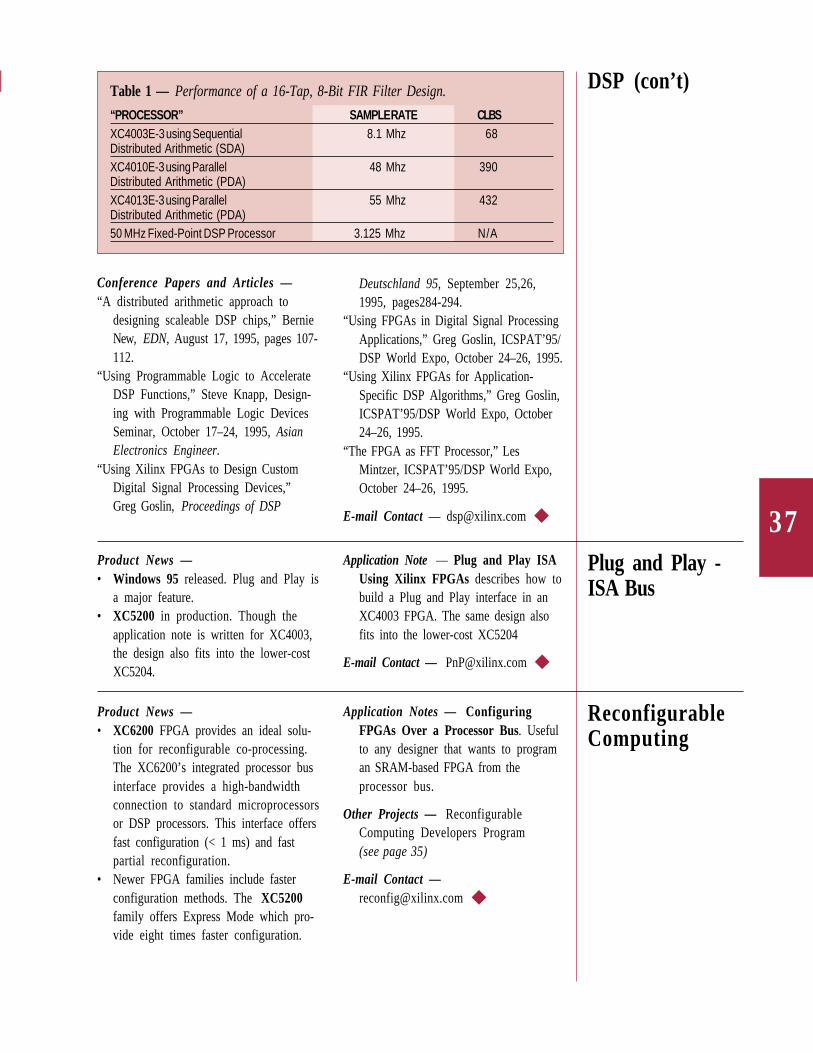
37
DSP (con’t)Table 1 — Performance of a 16-Tap, 8-Bit FIR Filter Design.
“PROCESSOR” SAMPLE RATE CLBSXC4003E-3 using Sequential 8.1 Mhz 68Distributed Arithmetic (SDA)XC4010E-3 using Parallel 48 Mhz 390Distributed Arithmetic (PDA)XC4013E-3 using Parallel 55 Mhz 432Distributed Arithmetic (PDA)50 MHz Fixed-Point DSP Processor 3.125 Mhz N/A
Conference Papers and Articles —“A distributed arithmetic approach to
designing scaleable DSP chips,” BernieNew, EDN, August 17, 1995, pages 107-112.
“Using Programmable Logic to AccelerateDSP Functions,” Steve Knapp, Design-ing with Programmable Logic DevicesSeminar, October 17–24, 1995, AsianElectronics Engineer.
“Using Xilinx FPGAs to Design CustomDigital Signal Processing Devices,”Greg Goslin, Proceedings of DSP
Deutschland 95, September 25,26,1995, pages284-294.
“Using FPGAs in Digital Signal ProcessingApplications,” Greg Goslin, ICSPAT’95/DSP World Expo, October 24–26, 1995.
“Using Xilinx FPGAs for Application-Specific DSP Algorithms,” Greg Goslin,ICSPAT’95/DSP World Expo, October24–26, 1995.
“The FPGA as FFT Processor,” LesMintzer, ICSPAT’95/DSP World Expo,October 24–26, 1995.
E-mail Contact — [email protected]
Plug and Play -ISA Bus
Product News —• Windows 95 released. Plug and Play is
a major feature.• XC5200 in production. Though the
application note is written for XC4003,the design also fits into the lower-costXC5204.
Application Note — Plug and Play ISAUsing Xilinx FPGAs describes how tobuild a Plug and Play interface in anXC4003 FPGA. The same design alsofits into the lower-cost XC5204
E-mail Contact — [email protected]
ReconfigurableComputing
Product News —• XC6200 FPGA provides an ideal solu-
tion for reconfigurable co-processing.The XC6200’s integrated processor businterface provides a high-bandwidthconnection to standard microprocessorsor DSP processors. This interface offersfast configuration (< 1 ms) and fastpartial reconfiguration.
• Newer FPGA families include fasterconfiguration methods. The XC5200family offers Express Mode which pro-vide eight times faster configuration.
Application Notes — ConfiguringFPGAs Over a Processor Bus. Usefulto any designer that wants to programan SRAM-based FPGA from theprocessor bus.
Other Projects — ReconfigurableComputing Developers Program(see page 35)
E-mail Contact —[email protected]
38
TECHNICAL QUESTIONS AND ANSWERS
EPLDMy design requires a 3.3 V output on theI/O pins of an XC7300 device. If I tieV
CCIO to a 3.3 V supply, can I still drive
inputs on the I/O pins at 5 V?Yes, when the V
CCIO pin is supplied by 3.3
V, only the logic output is affected. The thresh-olds on all input buffers are compatible withboth 5 V and 3.3 V inputs, and the ESD protec-tion diodes are connected to 5 V. There is noneed for external resistors.
I am using an ABEL source file for adesign on the XC7372. I have explicitlyassigned the critical signals to the fastinputs on the device. The timing reporthowever shows that they are treatingthem as standard I/O. How do I enablethe fast inputs?
The default configuration for ABEL is toroute the input pins through the UIM as anormal input. In order to utilize the fast inputs,you must explicitly declare them using theproperty statement in ABEL. For example, if
signals A, B, and C need to be fast inputs, usethe following statement in your ABEL file:
PLUSASM PROPERTY ‘INPUTPIN (FI)
A B C’;
I am using an XC7300 in a design with alarge number of input and outputsignals switching. I am concerned that Imay have problems with groundbounce. What can I do to minimize thispossibility?
There are several options to minimize po-tential ground bounce. If the system is de-signed for TTL levels, you may be able toconnect V
ccio to a 3.3 V supply voltage. This
will reduce the amount of current needed toswing outputs. Also, you can slow the outputslew rate from the default 1.5 V/ns to 1.0 V/nsby using the PLUSASM command,
FAST OFF <signal names>
or in ABEL,PLUSASM PROPERTY ‘FAST OFF
<signal names>’
ABELLooking at several ABEL files, I’venoticed that in some cases, the ORoperator appears as the # symbol and atother times as the + symbol. Is there adifference between the two?
ABEL supports two operator sets. Using thecommand
@alternate
invokes the alternative operator set. The fol-lowing table lists both sets.
ABEL Operator Alternative Description! / NOT& * AND# + OR$ :+: XOR!$ :*: XNOR
Note that while using the alternative opera-tors, the mathematical operators for addition,multiplication, and division are not available.
The standard ABEL operators, however, are stillin effect while using the alternative set. If youwish to mix the two, you can turn the alterna-tive operators off by using the command
@standard
What happens if I make multiple assign-ments to the same identifier in ABEL?
When ABEL finds multiple assignments to asingle identifier, they are logically ORed to-gether. If a complement operator is found onthe left side of an equation, then the comple-ment is performed after the expressions havebeen ORed. For example,
A = B;
A = !C;
!A = D;
!A = E;
is equivalent toA = B # !C # !(D # E);
39
SynopsysHow do I take a Synopsys design into aViewlogic schematic?
If you want to move a Synopsys designinto a Viewlogic schematic, then the Synopsysdesign must be converted into a .xnf file for aViewlogic schematic symbol. The procedureto follow is:1) Compile the design in Synopsys and write
out a .sxnf or .sedif file.2) run syn2xnf -s on the .sxnf/.sedif file.
For example, let’s say you’ve created adesign called count8. To bring count8 intoa Viewlogic schematic, type:syn2xnf -s count8
This will produce an .xnf file that can beused in a Viewlogic schematic.
How do I read an .xnf file intoSynopsys?1) Compile the design to an .lca file.2) Run lca2xnf on the .lca file.3) Run xnf2vss (xnf2vss is only in XSI 3.2 and
greater) on the .xnf file from step (2). This
will produce a file with the extension.vxnf
4) Rename the .vxnf file to a .xnf file.5) Read this renamed .xnf file into Synopsys.For example, if you have a .lca file calledcount.lca, lca2xnf would produce a file calledcount8.xnf. Next, xnf2vss would be run oncount8.xnf. A file called count8.vxnf wouldbe produced. Finally, after renamingcount8.vxnf to count8.xnf, now you will havea .xnf file that can be read into Synopsys.
Why does xnf2vss create a .vxnf fileand a .nrf file when it is run?
The .vxnf file is for reading a .xnf file intoSynopsys (see previous question). The .nrf fileshows how the .xnf names are changed forthe Synopsys VSS simulation flow. Synopsysand XACT using different naming conven-tions. So, when the .xnf is brought into VSS,sometimes the symbol names and netnamesin the .xnf file are modified. The .nrf file willshow you the modifications.
OrCADCan OrCAD Capture for Windows beused to enter designs in XACTstep?
The OrCAD interface in XACTstep is de-signed for use with SDT 386+. However, amethodology has been developed for usingCapture with XACTstep. The appropriate FPGAlibraries must be translated into OrCAD Cap-ture and selected during schematic entry.When adding properties or attributes to a com-ponent, they must be named using the defaultnames from OrCAD SDT. The schematic mustbe saved as an .SDF file. A document detailingthis methodology can be obtained using theXDOCS E-mail document retrieval system;please request document number 26121.
We currently recommend completing exist-ing designs in SDT 386+ before migrating toOrCAD Capture. The translation process canlose attributes that are not specified as PARTFIELD properties.
Mentor GraphicsHow can I obtain the latest copy of theXilinx Autologic libraries?
You can obtain the latest version of thelibraries (v1.2 as of October 1995) fromMentor’s FTP site at supportnet.mentorg.com(137.202.128.4).
These libraries are located in:/pub/mentortech/tdd/libraries/
fpga/xc2k_1.2.tar.Z
/pub/mentortech/tdd/libraries/
fpga/xc3k_1.2.tar.Z
/pub/mentortech/tdd/libraries/
fpga/xc4k_1.2.tar.Z
/pub/mentortech/tdd/libraries/
fpga/xc7k_1.2.tar.Z
These libraries are compatible with bothAutologic I and Autologic II.
40
FAX in Your Comments and SuggestionsTo: Brad Fawcett, XCELL Editor Xilinx Inc. FAX : 408-879-4676
From: ________________________________________ Date: ____________
Please add my name to the XCELL mailing list.
NAME
COMPANY
ADDRESS
CITY/STATE/ZIP
PHONE
I’m interested in having my company’s design featured in a future edition ofXCELL as a Customer Feature.
Comments and Suggestions:____________________________________________________________________________________________________________________________________________________________________________________________________________________________________________________________________________________________________________________________________________________________________________________________________________________________________________________________________________________________________________________________________________________________________________________________________________________________________________________________________________________________________________________________________________________________________________________________________________________________________________________________________________________________________________________________________________________________
Please use this form to FAX in your comments and suggestions, or to request an addition to theXCELL mailing list. Please feel free to make copies of this form for your colleagues.
U.S. PostagePAID
First ClassPermit No. 2196
San Jose, CA2100 Logic DriveSan Jose, CA 95124-3450
FAX RESPONSE FORM — XCELL 19 4Q95
CorporateHeadquartersXilinx, Inc.2100 Logic DriveSan Jose, CA 95124Tel: 408-559-7778Fax: 408-559-7114
EuropeXilinx, Ltd.Suite 1B, Cobb HouseOyster LaneByfleetSurrey KT147DUUnited KingdomTel: 44-1-932-349401Fax: 44-1-932-349499
JapanXilinx, KKDaini-Nagaoka Bldg. 2F2-8-5, Hatchobori,Chuo-ku, Tokyo 104JapanTel: 81-3-3297-9191Fax: 81-3-3297-9189
Asia PacificXilinx Asia PacificUnit 2308-2319 Tower 1MetroplazaHing Fong RoadKwai Fong, N.T.Hong KongTel: 852-2410-2739Fax: 852-2494-7159
R
Recommended