Embed Size (px)
Citation preview
2892 IEEE JOURNAL OF SOLID-STATE CIRCUITS, VOL. 46, NO. 12, DECEMBER 2011
Digital Approaches to ISI-Mitigation inHigh-Resolution Oversampled Multi-Level
D/A ConvertersLars Risbo, Member, IEEE, Rahmi Hezar, Member, IEEE, Burak Kelleci, Member, IEEE,
Halil Kiper, Member, IEEE, and Mounir Fares, Member, IEEE
Abstract—A new digital signal processing approach to shapingintersymbol interference (ISI) and static mismatch errors simul-taneously in oversampled multi-level digital to analog converters(DAC) has recently been proposed. In this paper, a mathematicalframework is established for analyzing ISI errors as well ascomparing the ISI sensitivities of different mismatch shapingalgorithms. The framework is used to analyze the fundamentalproblems of popularly used algorithms such as data-weighted-av-eraging (DWA) in the presence of nonlinear ISI: Large-signaleven-order distortion and frequency modulated harmonics at lowsignal levels. The new ISI-shaping algorithm results in significantimprovement over previous schemes including the modified Mis-match Shaper (MMS) which also addresses ISI error. The new ISIshaper, while increasing the digital complexity, practically elim-inates the need for conventional ISI mitigation techniques suchas time consuming, layout-critical, non-automated and processspecific analog design methods. The advantages of ISI shapingis further verified on an experimental audio DAC with simplenon-return-to-zero (NRZ) current steering segments implementedin a 45 nm CMOS process and running off a single-phase clock ofonly 3.072 MHz.
Index Terms—Audio, current-steering DAC, DAC, data-weighted averaging, digital-to-analog conversion, dynamic ele-ment matching, frequency modulation, idle tones, intersymbol-in-terference (ISI), ISI-shaping, mismatch shaping, noise shaping,non-return-to-zero (NRZ), out-of-band noise, sigma-delta modu-lation, vector quantizer.
I. INTRODUCTION
T HE current trend in high-performance audio DACs is touse fine resolution quantization to reduce the out-of-band
noise (OBN), reduce jitter sensitivity and simplify analog fil-tering. Recent techniques achieve this goal by using a mix ofDAC elements with different weights, e.g., segmenting [1] orcascading [2]. Unlike 1-bit modulation, the multi-level DACsneed mismatch shaping algorithms to compensate for the typ-ical 0.1–1% on-die static element mismatch. In addition to the
Manuscript received April 08, 2011; revised June 30, 2011; accepted July 29,2011. Date of publication October 03, 2011; date of current version November23, 2011. This paper was approved by Guest Editor Yiannos Manoli.
L. Risbo is with Texas Instruments Denmark A/S, DK-2800 Kgs. Lyngby,Denmark (e-mail: [email protected]).
R. Hezar is with Texas Instruments Inc., Dallas, TX 75243 USA.B. Kelleci is with the College of Engineering and Architecture, Okan Univer-
sity, Tuzla, Istanbul, 34959 Turkey.H. Kiper is with MediaTek, Woburn, MA 01801 USA.M. Fares is with Texas Instruments Inc., Dallas, TX 75243 USA.Color versions of one or more of the figures in this paper are available online
at http://ieeexplore.ieee.org.Digital Object Identifier 10.1109/JSSC.2011.2164965
element mismatch, dynamic error sources such as asymmet-rical switching, clock skew and parasitic memory are major hin-drances to achieve distortion and dynamic range targets. The re-sulting dependence of present symbol error to the past symbolis referred as intersymbol interference (ISI), and is a function ofthe switching activity of all the individual DAC-segments.
The first digital processing approach to mitigate circuit errorsis proposed in [3] with simple averaging of two current sources.Randomization [4] and individual-level-averaging (ILA) [5] arelater introduced for multi-level DACs. The very popular data-weighted-averaging (DWA) forms are first described in [6] and[7]. These algorithms can be found in many multi-level DACsand ADCs today due to their simple digital implementation ei-ther as a barrel shifter [6] or tree-branching [7]. Unfortunately,all of these methods [3]–[7] are addressing only the static mis-match problem. In addition, DWA algorithms [6], [7] increasethe switching activity, thus amplify ISI errors. Furthermore, theerror comes often in the form of spurious tones with signaldependent frequency (FM modulation [8]) that ruins the low-amplitude performance (e.g., harmonics for a 60 dB signal)which is critical for the perceived sound quality. A commonremedy is to add a digital DC offset to shift the tones out ofband. However, this merely moves the problematic amplituderegion, and does not solve the problem. Moreover, ISI errorsoften limit the large signal THD as a result of a strong signaldependent modulation of the element transition rate.
One popular analog solution to reduce ISI errors is to usethe return-to-zero (RTZ) approach which eliminates the de-pendence on the previous symbol, [9]. However, it leads toincreased current consumption, more high frequency compo-nents and higher sensitivity to circuit timing/jitter. Anotheranalog solution [1] is to use a track and hold circuit to deglitchthe waveform. However, such sampling circuits are sensitive toaliasing of high frequency noise. The Pulse Width Modulationmethod in [2] forces a fixed transition rate of the DAC elementsresulting in a significantly reduced sensitivity to ISI. However,this comes at the expense of a high clock rate which may notbe available in the system. This is also the case for the highlyinteresting DEM scheme of [10] with a fixed transition rate butwithout the intrinsic nonlinearity of PWM. Unfortunately, thisscheme puts severe restrictions to the noise shaper precedingthe DEM [10].
Recently, the “ISI-Shaper” DEM algorithm was introduced[11]. This algorithm provides concurrent spectral high-passshaping of static element mismatch and dynamic ISI errors. An
0018-9200/$26.00 © 2011 IEEE
RISBO et al.: DIGITAL APPROACHES TO ISI-MITIGATION IN HIGH-RESOLUTION OVERSAMPLED MULTI-LEVEL D/A CONVERTERS 2893
Fig. 1. ISI error waveforms for a binary DAC with a memory depth of onesymbol. (a) I. ideal DAC waveform, II. actual waveform, and III. ISI error wave-form with error integrals used for a discrete-time ISI signal representation in (1).(b) I. Actual waveform with error only on the falling edge, II. linearized wave-form by addition of a correction to the rising edge, III. linearized waveform byadding a correction to the 0� 0 transition.
earlier method specifically addressing the segment transitionrate and ISI without a need for an oversampled clock is themodified mismatch shaper (MMS) introduced in 1999 [12].
This paper compares the ISI shaper to the DWA (implementedby a barrels shifter rotation algorithm), MMS and second-orderDEM approaches with an implementation example in a 45 nmCMOS audio DAC. This design is taking advantage of morecomplex digital processing available in deep submicron CMOStechnology in order to obtain a high level of robustness to non-idealities of the analog design. This allows the use of a verysimple and non-critical analog section of the DAC with verylow power consumption and area.
Sections II and III provide a theoretical framework for theISI analysis. This mathematical modeling is then applied to thepopular DWA algorithm in Section IV where frequency modu-lation of idle tones resulting in low-level distortion is further an-alyzed. The DWA is compared to the second-order DEM, MMSand the proposed ISI shaping algorithm. Sections V and VI de-scribe the experimental results for a 45 nm audio DAC using theISI shaping method.
II. INTERSYMBOL INTERFERENCE MODELING
FOR 1-BIT SIGNALS
Almost any DAC can be decomposed into a number of sub-DACs that are summed with different weights. The symbol con-trolling each DAC-segment (sub-DAC) is typically from thebinary alphabet (i.e., a 1-bit signal, 1 or 0) and the symbol rateis equal to the DAC sample rate. Any memory-less nonlinearityacting on a 1-bit waveform will only result in an offset and gainerror since it only affects the current symbol. For a pure 1-bit
DAC, such error is benign. However, for a multi-level DACwith multiple 1-bit sub-DACs the gain errors cause nonlinearbehavior and need to be addressed by using a dynamic elementmatching algorithm. Intersymbol interference (ISI) is a wave-form distortion that is a function of the past symbols via variouscircuit memory effects. Such ISI errors can be nonlinear evenfor a single 1-bit DAC. This paper is restricted to analyzing ISIthat is a function of just the present and the previous symbolonly. For a discrete-time 1-bit signal there are 4 distinct inter-symbol transitions between the present and the previous symbolwhich are 0 0, 0 1, 1 0 and 1 1. Each transition typeis assumed to result in a specific transient error waveform thatdies out before the next symbol clock edge. Fig. 1 shows an ex-ample of such ISI error waveforms for all 4 transitions. To sim-plify the analysis, we will define a discrete-time signal asthe approximation to the continuous-time error waveform. Eachsample of is equal to the time integral of the error normal-ized by the clock period (the average error in the symbol clockperiod). The resulting discrete-time ISI signal is then a functionof the present and the past symbol and it is fully described bythe four values for each transition. With reference to Fig. 1 wehave
(1)
A common cause of ISI is any mismatch between the turn-onand turn-off delays when controlling a DAC-segment. This canbe caused by mismatches of the clock-to-Q delays of the risingand falling transitions of a D flip-flop. In addition, clock feed-through in the DAC circuit can cause a non-zero ISI error evenwhen the symbol does not change: and can in generalbe non-zero as in the example shown in Fig. 1. Assuming anideal non-return-to-zero (NRZ) DAC with finite transition de-lays and no clock feed-through error, we have
(2)
One-bit DAC waveforms with finite rise and fall times introduceISI errors similar to (2).
As a special case, the ISI function can be linear and has theform
(3)
In other words, the ISI error will be the DAC-segment signalfiltered by a 2-tap FIR filter defined by and plus a
DC offset as defined by . For a linear ISI error function, bycombining (1) and (3) we get
(4)
Equation (4) constitutes four linear equations with three un-knowns. The three unknowns, can be calculated as the
2894 IEEE JOURNAL OF SOLID-STATE CIRCUITS, VOL. 46, NO. 12, DECEMBER 2011
unique solution to three of the four linear equations in (4). Con-sequently, a linear ISI function is fully defined by three out ofthe four transition types. The fourth transition can then be foundby evaluating (4). This means that each of the four ISI errors ofa linear ISI error waveform can be expressed by a linear combi-nation of the other three errors:
(5)
For example, an NRZ waveform with ISI error according to(2) is linear if . In this case, the resulting segmentwaveform is simply delayed compared to the ideal waveformand the ISI function is a linear first-order high-pass filter (dif-ferentiator), and we have and .Similarly, a symmetrical rise and fall waveform for a pure NRZwithout glitches on the 0 0 and 1 1 transitions is a linearISI error. Fig. 1(b) shows a waveform with an ISI error onlyon the falling edge, i.e., a non-zero and
. Obviously, a compensating error with area ofadded to the falling edge would eliminate the ISI error. Alter-natively, the waveform would be linear if we added an error tothe rising edge to obtain an error area in accordance with (5):
. This leads to symmetrybetween rising and falling edges as shown in Fig. 1(b)-II. How-ever, as shown in Fig. 1(b)-III, we could also linearize the wave-form by adding the same error to the 0 0 transition to obtain
(opposite polarity of what hadto be added to the 0 1 transition). For completeness, the samecorrection could be added to the 1 1 transition to linearize theerror. Note that the linearized waveform of Fig. 1(b)-III doesnot have symmetry between rising and falling edges. It followsfrom the analysis that such rise/fall symmetry for waveformswith non-zero or is neither a sufficient or necessarycondition for linearity. The two linearized ISI error waveformsare obviously different which is also expressed in their respec-tive linear function parameters being different. In allcases, the same correction area was added or subtracted to asingle transition type to linearize the waveform. This correctionarea needed to linearize is a measure of the nonlinearity of theISI waveform. In other words, any ISI error can be decomposedinto a linear part and a nonlinear correction term occurring onlyfor one transition type. For the example given in (2), the cor-rection needed to linearize is equal to the mismatch between
and which is determined by the mismatch in risingand falling delays. The linear part of the ISI is of little practicalrelevance since this error is a DC offset and an AC part whichwill be high-pass shaped by the DEM algorithm. Throughoutthis paper, we assign the nonlinear ISI error arbitrarily only tothe ‘0 1’ transition. Furthermore, to facilitate comparisons ofdifferent DEM schemes, we normalize the ISI error magnitudeto unity and define the normalized transition function as
(6)
This function yields 0 for all transitions except for the 0 1case where the function is unity. This function is used to com-pare the ISI sensitivity for different DEM schemes since it rep-resents the nonlinear ISI error assigned to rising edges. We notethat for 1-bit sequences where only three out of four transitionsoccur, the -function will always be linear since we can fit alinear function conforming to (3) and (4).
The presented ISI analysis framework is consistent with [13,eq. (2)] where the DAC waveform is decomposed into threeterms: (a) a linear term, (b) a second-order nonlinear term, and(c) data-independent term. The data-independent term (c) be-comes a DC offset in the discrete-time domain and the nonlinearterm (b) corresponds to the transition function of (6) also re-ferred to as the “intersymbol product.”
For a binary alphabet, there is just one degree of freedom forthe nonlinear part of the ISI. However, some recent DACs [1]use a 3-symbol alphabet (e.g., 1, 0, 1) to control each DAC-segment. This method increases the amount of transition typesto and we have now degrees of freedom inthe nonlinear parts of the ISI which obviously complicates theanalysis.
III. THEORETICAL MAXIMUM TRANSITION DENSITY
FOR 1-BIT SIGNALS
We define the mean value of the -sequence in (6) as thetransition density, i.e., the mean density or the mean frequencyof rising edges. This will also be referred to as the transitionrate:
(7)
Similarly, we will define the DAC-segment density as
(8)
The segment usage density reflects the mean output signal ofthe specific segment. The purpose of a DEM is to make uniformusage of all segments, with identical segment densities that aremodulated linearly by the noise shaper and by the DAC inputsignal. This is in fact the purpose of a 1-bit sigma-delta modu-lator (pulse density modulator).
For a DAC with a bipolar output, the segment density canbe mapped to a modulation index that is between 1 and 1,normalized to full scale:
(9)
We will now derive bounds for the transition density of a 1-bitsignal. The analysis is restricted to periodic 1-bit sequences inorder to get a well-defined mean value. Since the period can bearbitrarily long, this is not limiting the scope of the results. Forany such periodic sequence, we note that the number of risingedge transitions can at most be equal to the number of ‘1’ sym-bols. Equality is obtained if and only if there are no ‘1 1’transitions. Because every ‘1’ can then only be preceded by a‘0’, the number of ‘0 1’ transitions and number of ‘1’s willbe equal. Whenever there is a ‘1 1’ transition in the sequence,
RISBO et al.: DIGITAL APPROACHES TO ISI-MITIGATION IN HIGH-RESOLUTION OVERSAMPLED MULTI-LEVEL D/A CONVERTERS 2895
we have a segment count increment without transition count in-crement. Consequently, the transition density is generally lessthan the segment density:
(10)
For any sequence without 0 0 transitions, we can fit thelinear function to the three other transitions ‘0 1’, ‘1 0’and ‘1 1’ by solving the three equations and three unknownsin (4) where the first row equation for is removed:
(11)
This means that
(12)
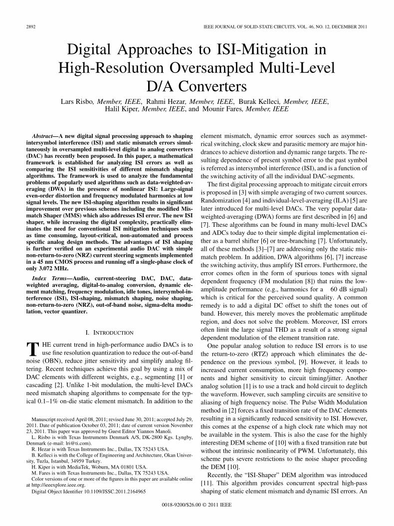
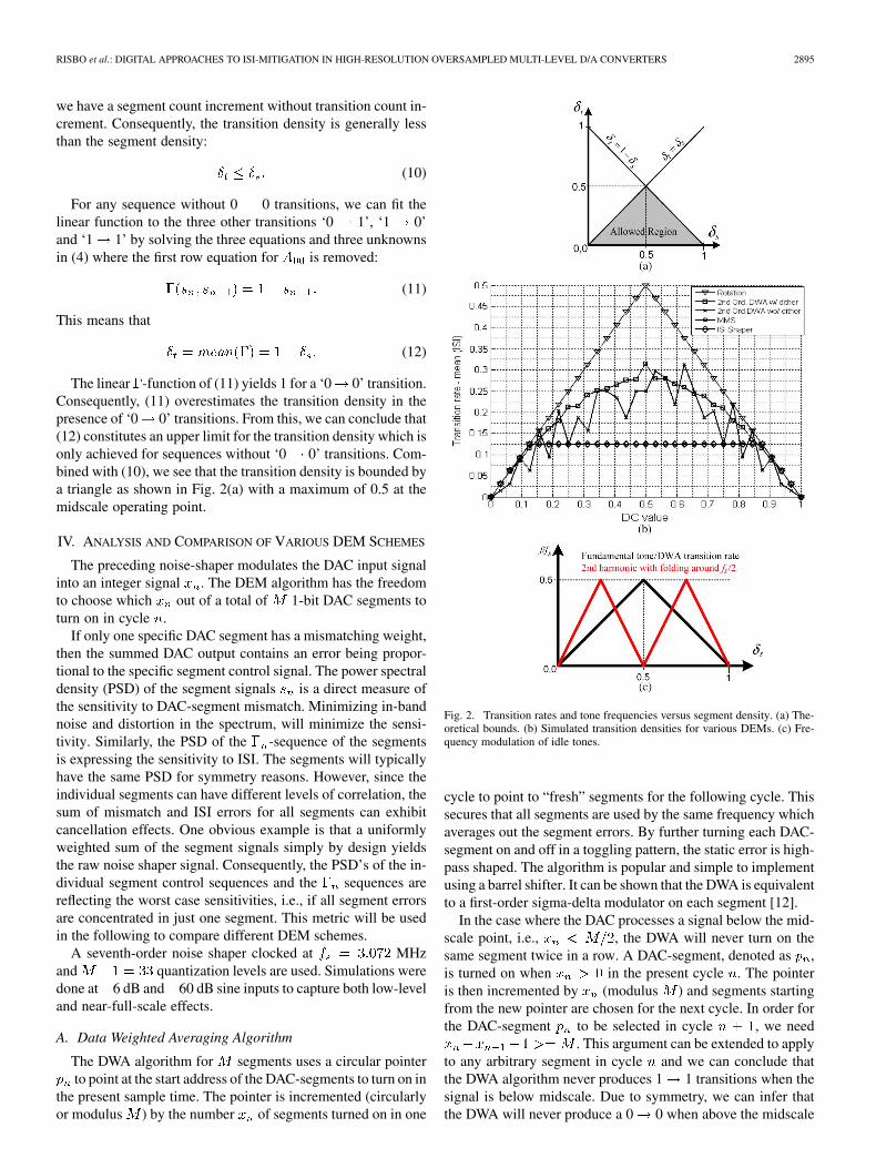
The linear -function of (11) yields 1 for a ‘0 0’ transition.Consequently, (11) overestimates the transition density in thepresence of ‘0 0’ transitions. From this, we can conclude that(12) constitutes an upper limit for the transition density which isonly achieved for sequences without ‘0 0’ transitions. Com-bined with (10), we see that the transition density is bounded bya triangle as shown in Fig. 2(a) with a maximum of 0.5 at themidscale operating point.
IV. ANALYSIS AND COMPARISON OF VARIOUS DEM SCHEMES
The preceding noise-shaper modulates the DAC input signalinto an integer signal . The DEM algorithm has the freedomto choose which out of a total of 1-bit DAC segments toturn on in cycle .
If only one specific DAC segment has a mismatching weight,then the summed DAC output contains an error being propor-tional to the specific segment control signal. The power spectraldensity (PSD) of the segment signals is a direct measure ofthe sensitivity to DAC-segment mismatch. Minimizing in-bandnoise and distortion in the spectrum, will minimize the sensi-tivity. Similarly, the PSD of the -sequence of the segmentsis expressing the sensitivity to ISI. The segments will typicallyhave the same PSD for symmetry reasons. However, since theindividual segments can have different levels of correlation, thesum of mismatch and ISI errors for all segments can exhibitcancellation effects. One obvious example is that a uniformlyweighted sum of the segment signals simply by design yieldsthe raw noise shaper signal. Consequently, the PSD’s of the in-dividual segment control sequences and the sequences arereflecting the worst case sensitivities, i.e., if all segment errorsare concentrated in just one segment. This metric will be usedin the following to compare different DEM schemes.
A seventh-order noise shaper clocked at MHzand quantization levels are used. Simulations weredone at 6 dB and 60 dB sine inputs to capture both low-leveland near-full-scale effects.
A. Data Weighted Averaging Algorithm
The DWA algorithm for segments uses a circular pointerto point at the start address of the DAC-segments to turn on in
the present sample time. The pointer is incremented (circularlyor modulus ) by the number of segments turned on in one
Fig. 2. Transition rates and tone frequencies versus segment density. (a) The-oretical bounds. (b) Simulated transition densities for various DEMs. (c) Fre-quency modulation of idle tones.
cycle to point to “fresh” segments for the following cycle. Thissecures that all segments are used by the same frequency whichaverages out the segment errors. By further turning each DAC-segment on and off in a toggling pattern, the static error is high-pass shaped. The algorithm is popular and simple to implementusing a barrel shifter. It can be shown that the DWA is equivalentto a first-order sigma-delta modulator on each segment [12].
In the case where the DAC processes a signal below the mid-scale point, i.e., , the DWA will never turn on thesame segment twice in a row. A DAC-segment, denoted as ,is turned on when in the present cycle . The pointeris then incremented by (modulus ) and segments startingfrom the new pointer are chosen for the next cycle. In order forthe DAC-segment to be selected in cycle , we need
. This argument can be extended to applyto any arbitrary segment in cycle and we can conclude thatthe DWA algorithm never produces 1 1 transitions when thesignal is below midscale. Due to symmetry, we can infer thatthe DWA will never produce a 0 0 when above the midscale
2896 IEEE JOURNAL OF SOLID-STATE CIRCUITS, VOL. 46, NO. 12, DECEMBER 2011
point. This means that the DWA is always producing sequenceswith the theoretical maximal transition density given by (10)and (12):
(13)
This result is confirmed by the simulation in Fig. 2(b) re-sulting in the same triangular pattern.
Both the transition density and ISI error is linear whenthe segment density stays above or below the midscale point(bipolar zero). In these piece-wise linear regions, the ISI erroris 100% correlated with the segment signal and is spectrallyhigh-pass shaped by the DWA algorithm. However, both thetransition density and the ISI signal are nonlinear when thesignal crosses the bipolar zero. This means that the ISI erroris de-correlated from the segment signal and is not generallyhigh-pass shaped like the segment signal. This discontinuity atthe bipolar zero makes the DWA algorithm very sensitive to ISI.
The transition density is a nonlinear function of the signal(segment density) due to the triangular shape. Using bipolarDAC output as defined by the modulation index , the transi-tion density of (13) can be rewritten as
(14)
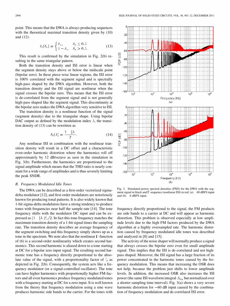
Any nonlinear ISI in combination with the nonlinear tran-sition density will result in a DC offset and a characteristiceven-order harmonic distortion where the harmonics roll offapproximately by 12 dB/octave as seen in the simulation inFig. 3(b). Furthermore, the harmonics are proportional to thesignal amplitude which means that the THD ratio is nearly con-stant for a wide range of amplitudes and is thus severely limitingthe peak SNDR.
B. Frequency Modulated Idle Tones
The DWA can be described as a first-order vectorized sigma-delta modulator [12], and first-order modulators are notoriouslyknown for producing tonal patterns. It is also widely known that1-bit sigma-delta modulators have a strong tendency to producetones with frequencies near half the sample rate [14]. The tonefrequency shifts with the modulator DC input and can be ex-pressed as . In fact this tone frequency matches themaximum transition density of a 1-bit signal times the samplingrate. The transition density describes an average frequency ofthe segment switching and this frequency simply shows up as atone in the spectrum. We note also that the nonlinear -functionof (6) is a second-order nonlinearity which creates second har-monics. This second harmonic is aliased down to a tone startingat DC for a bipolar zero input signal. The resulting second har-monic tone has a frequency directly proportional to the abso-lute value of the signal, with a proportionality factor of asdepicted in Fig. 2(b). Consequently, the system acts like a fre-quency modulator (or a signal-controlled oscillator). The tonecan have higher harmonics with proportionally higher FM-fac-tors and all even harmonics produce frequency modulated toneswith a frequency starting at DC for a zero input. It is well knownfrom the theory that frequency modulation using a sine waveproduces harmonic side bands to the carrier. For the tones with
Fig. 3. Simulated power spectral densities (PSD) for the DWA with the seg-ment signal in black and �-sequence (nonlinear ISI) in red: (a)�60 dBFS inputand (b) �6 dBFS input.
frequency directly proportional to the signal, the FM productsare side bands to a carrier at DC and will appear as harmonicdistortion. This problem is observed especially at low ampli-tude levels due to the high FM factors produced by the DWAalgorithm at a highly oversampled rate. The harmonic distor-tion caused by frequency modulated idle tones was describedand analyzed in [8] and [15].
The activity of the noise shaper will normally produce a signalthat always crosses the bipolar zero even for small amplitudesignal. This implies that the ISI is de-correlated and not high-pass shaped. Moreover, the ISI signal has a large fraction of itspower concentrated in the harmonic tones caused by the fre-quency modulation. This means that increasing the OSR doesnot help, because the problem just shifts to lower amplitudelevels. In addition, the increased OSR also increases the ISIpower (the same ISI waveform integral but normalized overa shorter sampling time interval). Fig. 3(a) shows a very severeharmonic distortion for 60 dB input caused by the combina-tion of frequency modulation and de-correlated ISI error.
RISBO et al.: DIGITAL APPROACHES TO ISI-MITIGATION IN HIGH-RESOLUTION OVERSAMPLED MULTI-LEVEL D/A CONVERTERS 2897
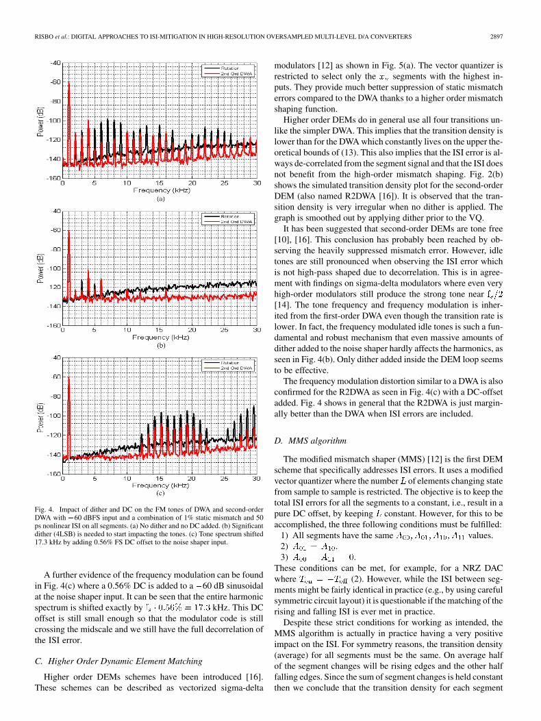
Fig. 4. Impact of dither and DC on the FM tones of DWA and second-orderDWA with �60 dBFS input and a combination of 1% static mismatch and 50ps nonlinear ISI on all segments. (a) No dither and no DC added. (b) Significantdither (4LSB) is needed to start impacting the tones. (c) Tone spectrum shifted17.3 kHz by adding 0.56% FS DC offset to the noise shaper input.
A further evidence of the frequency modulation can be foundin Fig. 4(c) where a 0.56% DC is added to a 60 dB sinusoidalat the noise shaper input. It can be seen that the entire harmonicspectrum is shifted exactly by kHz. This DCoffset is still small enough so that the modulator code is stillcrossing the midscale and we still have the full decorrelation ofthe ISI error.
C. Higher Order Dynamic Element Matching
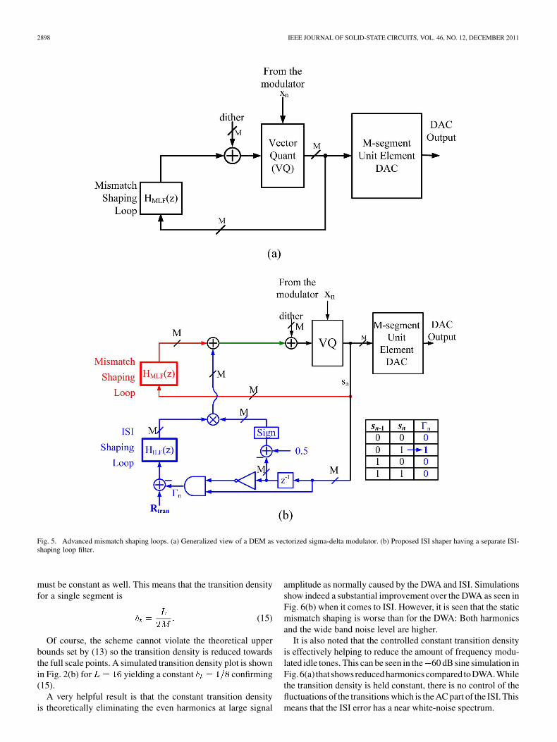
Higher order DEMs schemes have been introduced [16].These schemes can be described as vectorized sigma-delta
modulators [12] as shown in Fig. 5(a). The vector quantizer isrestricted to select only the segments with the highest in-puts. They provide much better suppression of static mismatcherrors compared to the DWA thanks to a higher order mismatchshaping function.
Higher order DEMs do in general use all four transitions un-like the simpler DWA. This implies that the transition density islower than for the DWA which constantly lives on the upper the-oretical bounds of (13). This also implies that the ISI error is al-ways de-correlated from the segment signal and that the ISI doesnot benefit from the high-order mismatch shaping. Fig. 2(b)shows the simulated transition density plot for the second-orderDEM (also named R2DWA [16]). It is observed that the tran-sition density is very irregular when no dither is applied. Thegraph is smoothed out by applying dither prior to the VQ.
It has been suggested that second-order DEMs are tone free[10], [16]. This conclusion has probably been reached by ob-serving the heavily suppressed mismatch error. However, idletones are still pronounced when observing the ISI error whichis not high-pass shaped due to decorrelation. This is in agree-ment with findings on sigma-delta modulators where even veryhigh-order modulators still produce the strong tone near[14]. The tone frequency and frequency modulation is inher-ited from the first-order DWA even though the transition rate islower. In fact, the frequency modulated idle tones is such a fun-damental and robust mechanism that even massive amounts ofdither added to the noise shaper hardly affects the harmonics, asseen in Fig. 4(b). Only dither added inside the DEM loop seemsto be effective.
The frequency modulation distortion similar to a DWA is alsoconfirmed for the R2DWA as seen in Fig. 4(c) with a DC-offsetadded. Fig. 4 shows in general that the R2DWA is just margin-ally better than the DWA when ISI errors are included.
D. MMS algorithm
The modified mismatch shaper (MMS) [12] is the first DEMscheme that specifically addresses ISI errors. It uses a modifiedvector quantizer where the number of elements changing statefrom sample to sample is restricted. The objective is to keep thetotal ISI errors for all the segments to a constant, i.e., result in apure DC offset, by keeping constant. However, for this to beaccomplished, the three following conditions must be fulfilled:
1) All segments have the same values.2) .3) .
These conditions can be met, for example, for a NRZ DACwhere (2). However, while the ISI between seg-ments might be fairly identical in practice (e.g., by using carefulsymmetric circuit layout) it is questionable if the matching of therising and falling ISI is ever met in practice.
Despite these strict conditions for working as intended, theMMS algorithm is actually in practice having a very positiveimpact on the ISI. For symmetry reasons, the transition density(average) for all segments must be the same. On average halfof the segment changes will be rising edges and the other halffalling edges. Since the sum of segment changes is held constantthen we conclude that the transition density for each segment
2898 IEEE JOURNAL OF SOLID-STATE CIRCUITS, VOL. 46, NO. 12, DECEMBER 2011
Fig. 5. Advanced mismatch shaping loops. (a) Generalized view of a DEM as vectorized sigma-delta modulator. (b) Proposed ISI shaper having a separate ISI-shaping loop filter.
must be constant as well. This means that the transition densityfor a single segment is
(15)
Of course, the scheme cannot violate the theoretical upperbounds set by (13) so the transition density is reduced towardsthe full scale points. A simulated transition density plot is shownin Fig. 2(b) for yielding a constant confirming(15).
A very helpful result is that the constant transition densityis theoretically eliminating the even harmonics at large signal
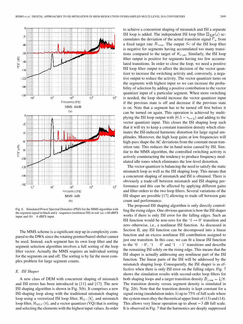
amplitude as normally caused by the DWA and ISI. Simulationsshow indeed a substantial improvement over the DWA as seen inFig. 6(b) when it comes to ISI. However, it is seen that the staticmismatch shaping is worse than for the DWA: Both harmonicsand the wide band noise level are higher.
It is also noted that the controlled constant transition densityis effectively helping to reduce the amount of frequency modu-lated idle tones. This can be seen in the 60 dB sine simulation inFig.6(a) that showsreducedharmonicscompared toDWA.Whilethe transition density is held constant, there is no control of thefluctuations of the transitions which is the AC part of the ISI. Thismeans that the ISI error has a near white-noise spectrum.
RISBO et al.: DIGITAL APPROACHES TO ISI-MITIGATION IN HIGH-RESOLUTION OVERSAMPLED MULTI-LEVEL D/A CONVERTERS 2899
Fig. 6. Simulated Power Spectral Densities (PSD) for the MMS algorithm withthe segment signal in black and�-sequence (nonlinear ISI) in red: (a)�60 dBFSinput and (b) �6 dBFS input.
The MMS scheme is a significant step up in complexity com-pared to the DWA since the rotating pointer/barrel shifter cannotbe used. Instead, each segment has its own loop filter and thesegment selection algorithm involves a full sorting of the loopfilter vector. Actually the MMS requires an individual sortingfor the segments on and off. The sorting is by far the most com-plex problem for large segment counts.
E. ISI Shaper
A new class of DEM with concurrent shaping of mismatchand ISI errors has been introduced in [11] and [17]. The newISI shaping algorithm is shown in Fig. 5(b). It comprises a newISI-shaping loop along with the traditional mismatch shapingloop using a vectorized ISI loop filter, , and mismatchloop filter, , and a vector quantizer (VQ) that is sortingand selecting the elements with the highest input values. In order
to achieve a concurrent shaping of mismatch and ISI a separateISI loop is added. The independent ISI loop filter ac-cumulates the deviation of the actual transition signal froma fixed target rate . The output of the ISI loop filteris negative for segments having accumulated too many transi-tions compared to the target of . Similarly, the ISI loopfilter output is positive for segments having too few accumu-lated transitions. In order to close the loop, we need a positiveISI loop filter output to affect the decision of the vector quan-tizer to increase the switching activity and, conversely, a nega-tive output to reduce the activity. The vector quantizer turns onthe segments with highest input so we can increase the proba-bility of selection by adding a positive contribution to the vectorquantizer input of a particular segment. When more switchingis needed, the loop should increase the vector quantizer inputif the previous state is off and decrease if the previous stateis on. Note that a segment has to be turned off first before itcan be turned on again. This operation is achieved by multi-plying the ISI loop output with and adding to thevector quantizer input. This closes the ISI shaping loop suchthat it will try to keep a constant transition density which elim-inates the ISI-induced harmonic distortion for large signal am-plitudes. Moreover, the high loop gains at low frequencies willhigh-pass shape the AC deviations from the constant mean tran-sition rate. This reduces the in-band noise caused by ISI. Sim-ilar to the MMS algorithm, the controlled switching activity isactively counteracting the tendency to produce frequency mod-ulated idle tones which eliminates the low-level distortion.
The vector quantizer is balancing the need to satisfy the staticmismatch loop as well as the ISI shaping loop. This means thata concurrent shaping of mismatch and ISI is obtained. There isobviously a trade-off between mismatch and ISI shaping per-formance and this can be affected by applying different gainsand filter orders to the two loop filters. Several variations of theISI shaper are possible [17] allowing to trade off between gatecount and performance.
The proposed ISI shaping algorithm is only directly control-ling the rising edges. One obvious question is how the ISI shaperworks if there is only ISI error for the falling edges. Such anISI function would be non-zero for the ‘1 0’ transition andzero otherwise, i.e., a nonlinear ISI function. As discussed inSection II, any ISI function can be decomposed into a linearfunction and an excess nonlinear ISI contribution assigned tojust one transition. In this case, we can fit a linear ISI functionto the ‘0 0’, ‘1 0’ and ‘1 1’ transitions and describethe remaining ISI solely on the rising edge. This means that theISI shaper is actually addressing any nonlinear part of the ISIfunction. The linear parts of the ISI will be addressed by themismatch shaping loop. Consequently, the ISI shaper is as ef-fective when there is only ISI error on the falling edges. Fig. 7shows the simulation results with second-order loop filters forboth shaping loops and a target transition density .The transition density versus segment density is simulated inFig. 2(b). Note that the transition density is kept constant for asignal swing (modulation index ) up to 75% of full scale wherethe system must obey the theoretical upper limit of (13) and (14).This allows very linear operation up to about 3 dB full scale.It is observed in Fig. 7 that the harmonics are deeply suppressed
2900 IEEE JOURNAL OF SOLID-STATE CIRCUITS, VOL. 46, NO. 12, DECEMBER 2011
Fig. 7. Simulated power spectral densities (PSD) for the ISI shaper algorithm(second-order for both loops) with the segment signal in black and �-sequence(nonlinear ISI) in red: (a) �60 dBFS input and (b) �6 dBFS input.
both at 6 dB and 60 dB and that there is a similar and con-current second-order high-pass shaping of both the mismatchand nonlinear ISI error. The spectral shaping of the nonlinearISI is a significant improvement over the MMS scheme whichis achieved through the use of the separate ISI shaping loop filterwhich controls the switching activity individually for each seg-ment.
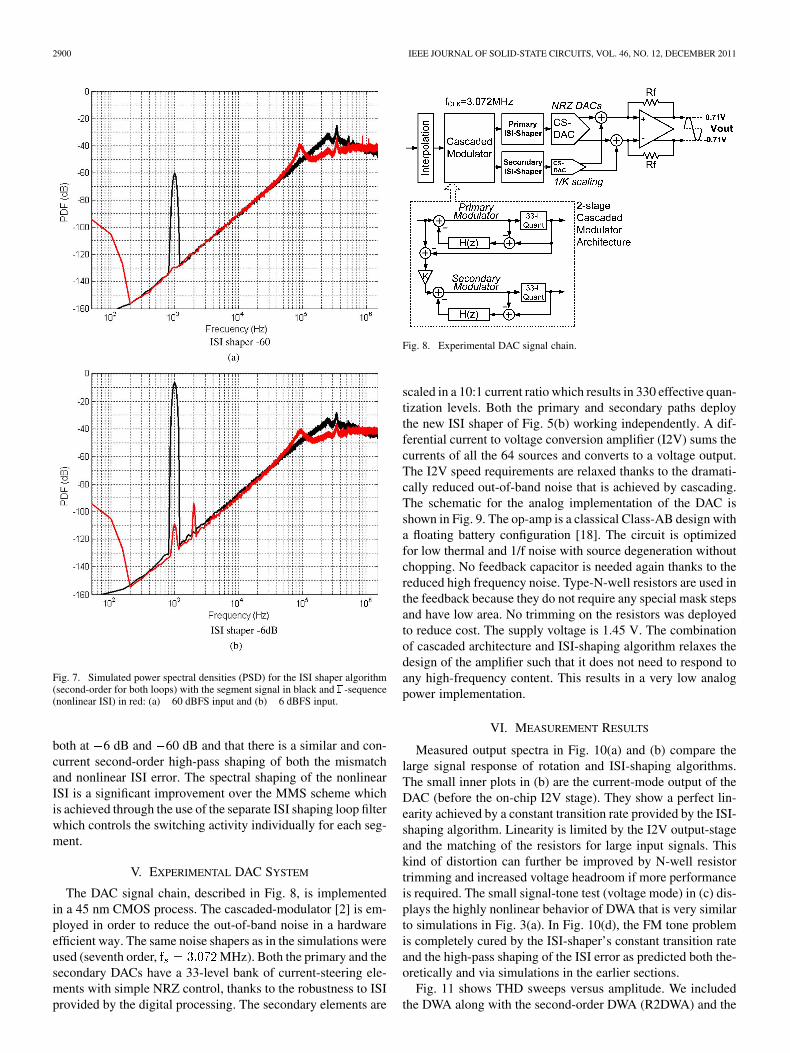
V. EXPERIMENTAL DAC SYSTEM
The DAC signal chain, described in Fig. 8, is implementedin a 45 nm CMOS process. The cascaded-modulator [2] is em-ployed in order to reduce the out-of-band noise in a hardwareefficient way. The same noise shapers as in the simulations wereused (seventh order, MHz). Both the primary and thesecondary DACs have a 33-level bank of current-steering ele-ments with simple NRZ control, thanks to the robustness to ISIprovided by the digital processing. The secondary elements are
Fig. 8. Experimental DAC signal chain.
scaled in a 10:1 current ratio which results in 330 effective quan-tization levels. Both the primary and secondary paths deploythe new ISI shaper of Fig. 5(b) working independently. A dif-ferential current to voltage conversion amplifier (I2V) sums thecurrents of all the 64 sources and converts to a voltage output.The I2V speed requirements are relaxed thanks to the dramati-cally reduced out-of-band noise that is achieved by cascading.The schematic for the analog implementation of the DAC isshown in Fig. 9. The op-amp is a classical Class-AB design witha floating battery configuration [18]. The circuit is optimizedfor low thermal and 1/f noise with source degeneration withoutchopping. No feedback capacitor is needed again thanks to thereduced high frequency noise. Type-N-well resistors are used inthe feedback because they do not require any special mask stepsand have low area. No trimming on the resistors was deployedto reduce cost. The supply voltage is 1.45 V. The combinationof cascaded architecture and ISI-shaping algorithm relaxes thedesign of the amplifier such that it does not need to respond toany high-frequency content. This results in a very low analogpower implementation.
VI. MEASUREMENT RESULTS
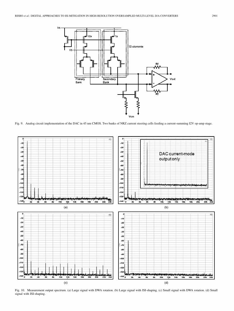
Measured output spectra in Fig. 10(a) and (b) compare thelarge signal response of rotation and ISI-shaping algorithms.The small inner plots in (b) are the current-mode output of theDAC (before the on-chip I2V stage). They show a perfect lin-earity achieved by a constant transition rate provided by the ISI-shaping algorithm. Linearity is limited by the I2V output-stageand the matching of the resistors for large input signals. Thiskind of distortion can further be improved by N-well resistortrimming and increased voltage headroom if more performanceis required. The small signal-tone test (voltage mode) in (c) dis-plays the highly nonlinear behavior of DWA that is very similarto simulations in Fig. 3(a). In Fig. 10(d), the FM tone problemis completely cured by the ISI-shaper’s constant transition rateand the high-pass shaping of the ISI error as predicted both the-oretically and via simulations in the earlier sections.
Fig. 11 shows THD sweeps versus amplitude. We includedthe DWA along with the second-order DWA (R2DWA) and the
RISBO et al.: DIGITAL APPROACHES TO ISI-MITIGATION IN HIGH-RESOLUTION OVERSAMPLED MULTI-LEVEL D/A CONVERTERS 2901
Fig. 9. Analog circuit implementation of the DAC in 45 nm CMOS. Two banks of NRZ current steering cells feeding a current-summing I2V op-amp stage.
Fig. 10. Measurement output spectrum. (a) Large signal with DWA rotation. (b) Large signal with ISI-shaping. (c) Small signal with DWA rotation. (d) Smallsignal with ISI-shaping.
2902 IEEE JOURNAL OF SOLID-STATE CIRCUITS, VOL. 46, NO. 12, DECEMBER 2011
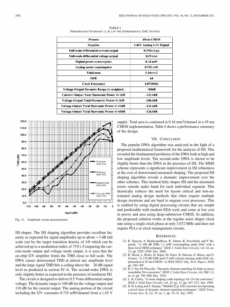
TABLE IPERFORMANCE SUMMARY (1 ch.) OF THE EXPERIMENTAL DAC SYSTEM
Fig. 11. Amplitude sweep measurements.
ISI-shaper. The ISI shaping algorithm provides excellent lin-earity as expected for signal amplitudes up to about 3 dB fullscale (set by the target transition density of 1/8 which can beachieved up to a modulation index of 75%). Comparing the cur-rent-mode output and voltage mode output, it is seen that theon-chip I2V amplifier limits the THD close to full scale. TheDWA causes deteriorated THD at almost any amplitude leveland the large signal THD hits a ceiling above the 20 dB signallevel as predicted in section IV-A. The second-order DWA isonly slightly better as expected in the presence of nonlinear ISI.
The circuit is designed to deliver 0.5 Vrms differential outputvoltage. The dynamic range is 108 dB for the voltage output and110 dB for the current output. The analog portion of the circuitincluding the I2V consumes 0.735 mW/channel from a 1.45 V
supply. Total area is contained at 0.16 mm /channel in a 45 nmCMOS implementation. Table I shows a performance summaryof the design.
VII. CONCLUSION
The popular DWA algorithm was analyzed in the light of aproposed mathematical framework for the analysis of ISI. Thisrevealed the fundamental problems of the DWA both at high andlow amplitude levels. The second-order DWA is shown to beslightly better than the DWA in the presence of ISI. The MMSscheme represents a significant improvement in ISI robustnessat the cost of deteriorated mismatch shaping. The proposed ISIshaping algorithm reveals a dramatic improvement over theother schemes. This method fully shapes ISI and the mismatcherrors outside audio band for each individual segment. Thisdrastically reduces the need for layout critical and non-au-tomated analog design methods that often require multipledesign iterations and are hard to migrate over processes. Thisis enabled by using digital processing circuits that are simpleand predictable with modern EDA tools and come at low costin power and area using deep-submicron CMOS. In addition,the proposed solution works at the regular noise shaper clockrate using a single clock phase at only 3.072 MHz and does notrequire PLLs or clock management circuits.
REFERENCES
[1] K. Nguyen, A. Bandyopadhyay, R. Adams, K. Sweetland, and P. Ba-ginski, “A 108 dB SNR, 1.1 mW oversampling audio DAC with athree-level DEM technique,” IEEE J. Solid-State Circuits, vol. 42, no.12, pp. 2592–2599, Dec. 2008.
[2] R. Hezar, L. Risbo, H. Kiper, M. Fares, B. Haroun, G. Burra, and G.Gomez, “A 110 dB SNR and 0.5 mW current-steering audio DAC im-plemented in 45 nm CMOS,” in IEEE ISSCC Dig. Tech. Papers, 2010,pp. 304–305.
[3] R. J. Van De Plassche, “Dynamic element matching for high accuracymonolithic DA converters,” IEEE J. Solid-State Circuits, vol. SSC-11,no. 6, pp. 795–800, Dec. 1976.
[4] L. R. Carley, “A noise shaping coder topology for 15+ bit converters,”IEEE J. Solid-State Circuits, vol. 24, no. 12, pp. 267–273, Apr. 1989.
[5] B. H. Leung and S. Sutarja, “Multibit�� A/D converter incorporatinga novel class of dynamic element matching techniques,” IEEE Trans.Circuits Syst. II, vol. 39, no. 1, pp. 35–51, Jan. 1992.
RISBO et al.: DIGITAL APPROACHES TO ISI-MITIGATION IN HIGH-RESOLUTION OVERSAMPLED MULTI-LEVEL D/A CONVERTERS 2903
[6] R. T. Baird and T. S. Fiez, “Linearity enhancement of multibit ��A/D and D/A converters using data weighted averaging,” IEEE Trans.Circuits Syst. II, vol. 42, no. 12, pp. 753–762, Dec. 1995.
[7] I. Galton, “Spectral shaping of circuit errors in digital-to-analog con-verters,” IEEE Trans. Circuits Syst. II, vol. 44, no. 10, pp. 808–817,Oct. 1997.
[8] L. Risbo, “Low-level distortion, tones, tone-extraction and FM modu-lation in D/A converters,” presented at the Workshop W9—The Howsand Whys of Sigma Delta Converters, Audio Engineering Society122nd Convention, Vienna, Austria, May 2007.
[9] K. Nguyen, R. Adams, and K. Sweetland, “A 113 dB SNR oversam-pling Sigma-Delta DAC for CD/DVD application,” IEEE Trans. Con-sumer Electron., vol. 44, no. 3, pp. 1019–1023, Jun. 1998.
[10] D. Reefman et al., “A new digital-to-analog converter design for HiFiapplications,” presented at the 114th Audio Engineering Society Con-vention, Mar. 2003, paper 5846.
[11] L. Risbo, R. Hezar, B. Kelleci, H. Kiper, and M. Fares, “A 108 dBDR, 120 dB THD and 0.5 Vrms output audio DAC with intersymbolinterference shaping algorithm in 45 nm,” in IEEE ISSCC Dig. Tech.Papers, 2011, pp. 484–485.
[12] T. Shui, R. Schreier, and F. Hudson, “Mismatch shaping for a current-mode multi-bit delta-sigma DAC,” IEEE J. Solid-State Circuits, vol.34, no. 3, pp. 331–338, Mar. 1999.
[13] Q. Mu, J. O. Coleman, D. P. Scholnik, and Z. Popovic, “Circuit ap-proaches to nonlinear-ISI mitigation in noise-shaped bandpass D/Aconversion,” IEEE Trans. Circuits Syst. I, vol. 57, no. 7, pp. 1559–1572,Jul. 2010.
[14] L. Risbo, “On the design of tone-free sigma-delta modulators,” IEEETrans. Circuits Syst. II, vol. 42, no. 1, pp. 52–55, Jan. 1995.
[15] S. P. Lipshitz and J. Vanderkooy, “Towards a better understanding of1-bit sigma-delta modulators—Part 2,” presented at the 111th AudioEngineering Society Convention, Sep. 2001, paper 5477.
[16] X. M. Gong, “An efficient second-order dynamic element matchingtechnique for a 120 dB multiple-bit delta-sigma DAC,” presented at the108th Audio Engineering Society Convention, Feb. 2000, paper 5124.
[17] L. Risbo, R. Hezar, B. Kelleci, and A. B. Josefsen, “Shaping inter-symbol interference in sigma delta converter,” , filed to U.S. PatentOffice April 28, 2010, application number 12/769,629.
[18] I. Padilla-Cantoya, “Dual-polarity floating battery for Class AB outputstages with accurate quiescent current control,” in Proc. IEEE MidwestSymp. Circuits and Systems, 2007, pp. 887–890.
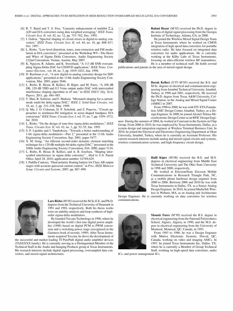
Lars Risbo (M’05) received the M.Sc.E.E. and Ph.D.degrees from the Technical University of Denmark in1991 and 1994, respectively. Both his thesis workswere on stability analysis and loop synthesis of high-order sigma-delta modulators.
He founded Toccata Technology in 1996, where hedeveloped the world’s first true digital power ampli-fier (1998) based on digital PCM to PWM conver-sion and a switching power stage (recognized in theGuinness book of records, 1999). After Texas Instru-ments acquired Toccata, he drove the development of
the successful and market leading TI PurePath digital audio amplifier devices(TASXXXX family). He is currently serving as a Distinguished Member of theTechnical Staff in the Audio and Imaging Products group at Texas Instruments.His research interests include digital signal processing, oversampled data con-verters, and mixed-signal architectures.
Rahmi Hezar (M’02) received the Ph.D. degree inthe area of digital signal processing from the GeorgiaInstitute of Technology, Atlanta, GA, in 2000.
He joined the Wireless Mixed Signal Design Teamat Texas Instruments where he worked on CMOSintegration of high speed data converters for portablewireless radio. He later focused on integrated dataconverters for audio applications. He is currentlyworking at the Kilby Labs of Texas Instruments,focusing on ultra-efficient wireless RF transmitters.He is a member of technical staff. He holds several
publications and patents in the area of mixed-signal design.
Burak Kelleci (S’97–M’05) received the B.S. andM.Sc. degrees in electrical and communication engi-neering from Istanbul Technical University, Istanbul,Turkey, in 1998 and 2001, respectively. He receivedthe Ph.D. degree from Texas A&M University, Col-lege Station, in the Analog and Mixed Signal Center(AMSC) in 2007.
From 1998 to 2000, he was with ITU ETA Founda-tion ASIC Design Center, Istanbul, Turkey, as a De-sign Engineer. In 2000, he joined Alcatel-Teletas Mi-croelectronic Design Center as an RFIC Design Engi-
neer. During the summer of 2004, he worked at Conexant in the System on ChipGroup. From 2006 to 2010, he was employed by Texas Instruments, Dallas, as asystem design and integration engineer at Wireless Terminal Business Unit. In2010, he joined the Electrical and Electronics Engineering Department at OkanUniversity, Istanbul, Turkey, where he is currently an Assistant Professor. Hiscurrent research interests include analog and mixed-signal circuits and systems,wireless communication systems, and high-frequency circuit design.
Halil Kiper (M’08) received the B.S. and M.S.degrees in electrical engineering from Middle EastTechnical University and The Ohio State Universityin 1998 and 2000, respectively.
He worked at Ericsson/Sony Ericsson MobileCommunications in Research Triangle Park, NC,as a mobile phone hardware design engineer from2000 to 2006. Between 2006 and 2010 he was withTexas Instruments in Dallas, TX, as a Senior AnalogDesign Engineer. In 2010, he joined MediaTek Wire-less in Woburn, MA, as an Analog and Architecture
Design Engineer. He is currently working on data converters for wirelesscommunications.
Mounir Fares (M’99) received the B.S. degree inelectrical engineering from the National PolytechnicsSchool, Algiers, Algeria, in 1990, and the M.S. de-gree in electrical engineering from the University ofMontreal, Montreal, QC, Canada, in 1993.
From 1993 to 1996, he was a Design Engineerwith Matrox Electronic Systems, Dorval, QC,Canada, working on video and imaging ASICs. In1997, he joined Texas Instruments Inc, Dallas, TX,where he is currently a Member of Group TechnicalStaff, working on high-speed data converters, audio
ICs, and power management ICs.