Embed Size (px)
Citation preview
Silicon Integrated Circuits Incorporating Antennas
K. K. O, K. Kim, B. Floyd, J. Mehta, H. Yoon, C.-M. Hung, D. Bravo, T. Dickson, X. Guo, R. Li, N. Trichy, J. Caserta, W. Bomstad, J. Branch, D.-J. Yang, J. Bohorquez, J. Chen, E.-Y. Seok, J. E. Brewer, L. Gao, A. Sugavanam, J.-J. Lin, Y. Su, C. Cao, M.-H. Hwang, Y.-P. Ding, Z. Li, S.-H. Hwang, H. Wu,
S. Sankaran, and N. Zhang
(Invited)
Silicon Microwave Integrated Circuits and System Research Group (SiMICS)Department of Electrical and Computer Engineering, University of Florida, Gainesville, FL, 32611
Tel.: 352-392-6618, e-mail: [email protected]
IEEE 2006 Custom Intergrated Circuits Conference (CICC)
Abstract-The feasibility of integrating antennas and requiredcircuits to form wireless interconnects in foundry digitalCMOS technologies has been demonstrated. The key chal-lenges including the effects of metal structures associatedwith integrated circuits, heat removal, packaging, and inter-action of transmitted and received signals with nearby cir-cuits appear to be manageable. This technology canpotentially be used for intra and inter-chip interconnection,and implementation of true single chip radios, beacons,radars, RFID tags and others, as well as contact-less high fre-quency testing.
Introduction Scaling of MOS transistor lengths to nano scale has made
the implementation of CMOS circuits operating at 20 GHzand higher feasible [1]-[5]. According to the 2005 Interna-tional Road Map for Semiconductors (ITRS) [6], the cut-offfrequency (fT) and unity maximum available power gain fre-quency (fmax) targets for the year 2015 are ~500 and700GHz. With such transistors, it should be possible toimplement RF circuits operating at 200-250 GHz. In fact,recent demonstrations of a 192-GHz oscillator [7] and a 182-GHz Schottky detector [8] using 130-nm CMOS suggest thatthe 200-250GHz operating frequency projection are conser-
vative. At 24GHz, a wavelength of electro-magnetic waves infree space is 12.5 mm and in silicon it is 3.7 mm. This meansa quarter wave antenna needs to be only ~ 3 and 0.9 mm infree space and silicon. At 250 GHz, a quarter wave antennaneeds to be ~300 and ~90 µm in free space and silicon. Thesein conjunction with the increases of chip sizes to ~ 2 cm x 2cm have made the integration of antennas possible.
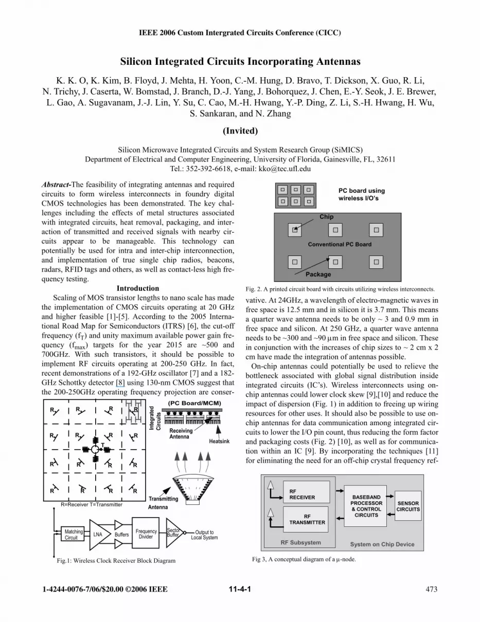
On-chip antennas could potentially be used to relieve thebottleneck associated with global signal distribution insideintegrated circuits (IC’s). Wireless interconnects using on-chip antennas could lower clock skew [9],[10] and reduce theimpact of dispersion (Fig. 1) in addition to freeing up wiringresources for other uses. It should also be possible to use on-chip antennas for data communication among integrated cir-cuits to lower the I/O pin count, thus reducing the form factorand packaging costs (Fig. 2) [10], as well as for communica-tion within an IC [9]. By incorporating the techniques [11]for eliminating the need for an off-chip crystal frequency ref-
FrequencyDividerLNAMatching Buffers Buffer
Sector Output toLocal System
Fig.1: Wireless Clock Receiver Block Diagram
R=Receiver T=Transmitter
Inte
grat
edCi
rcui
ts
Transmitting
Receiving Antenna
Heatsink
Antenna
(PC Board/MCM)
Circuit
T
R
R
R
R R R
R R R
R R R
R R R R
Fig. 2. A printed circuit board with circuits utilizing wireless interconnects.
PC board using wireless I/O’s
Conventional PC Board
Chip
Package
Fig 3, A conceptual diagram of a µ-node.
RF RECEIVER
RF TRANSMITTER
BASEBAND PROCESSOR & CONTROL
CIRCUITS
SENSOR CIRCUITS
RF Subsystem System on Chip Device
RF RECEIVER
RF TRANSMITTER
BASEBAND PROCESSOR & CONTROL
CIRCUITS
SENSOR CIRCUITS
RF Subsystem System on Chip Device
1-4244-0076-7/06/$20.00 ©2006 IEEE 47311-4-1
erence into a transceiver with on-chip antennas, a true singlechip radio which is small, reliable and easy to use could alsobe realized [12]. The availability of sensor nodes incorporat-ing such radios (µ-nodes, Fig. 3) should accelerate the real-ization of the Smart Dust vision [13].
This paper reviews the background, potential applicationswhich could benefit from utilizing on-chip antennas, and sta-tus of key technologies required to implement the systems forthese applications as well as challenges and potential solu-tions. In particular, this paper discusses the characteristics ofon-chip antennas fabricated on 10-20 Ω-cm silicon substratescommonly used in CMOS and BiCMOS technologies [14]-[18] and circuits incorporating on-chip antennas [19]-[26]within the context of applications [10]. The key challengesincluding the effects of metal structures associated with inte-grated circuits [27]-[30], heat removal [31],[32], packaging[33], and interaction of transmitted and received signals withnearby circuits [34]-[39] are discussed.
On-chip antennasFabrication of antennas on a semiconducting substrate pre-
dates the recent research activities by at least 10 years. Anon-chip antenna integrated with a 95-GHz IMPATT diodeoscillator on a high resistivity silicon substrate [40] and anon-chip antenna integrated with a 43.3-GHz IMPATT diodeoscillator on a GaAs substrate [41] have been reported in1986 and 1988, respectively. High resistivity silicon sub-strates have also been used to fabricate MEMS based anten-nas operating at 90 to 802 GHz [42]. Because of the use ofIMPATT diode circuits, the types of radio systems that couldbe built are limited. Furthermore, the substrates are not com-patible to the low cost mainstream silicon process technolo-gies with high levels of integration.
For most applications, to make on-chip antennas viable,they must be inexpensive to incorporate. This means, besidesthe substrate compatibility, the antennas must be fabricatedusing the conductor and dielectric layers available in main-stream silicon technologies. Presently, the number of metallayers can be as high as 10 with a thickness ranging between~0.2 to 3 µm. The conductors can be either aluminum or cop-per. The dielectric layers separating the conductors are varia-tions of SiO2 with thicknesses ranging between 0.2 to 1 µm.Because, the conductor and dielectric layers can be stacked,the total conductor and dielectric thicknesses can be ~2-5µm. Fig. 4 shows linear dipole, zigzag dipole, and loopantennas fabricated on silicon substrates [14]-[18]. The struc-tures have been chosen over the patch type because of theircompactness. For 24-GHz applications, a typical antenna
occupies ~3-4mm x 0.15mm. In volume production, such anantenna is expected to add ~ 1-2 cents to the die cost.
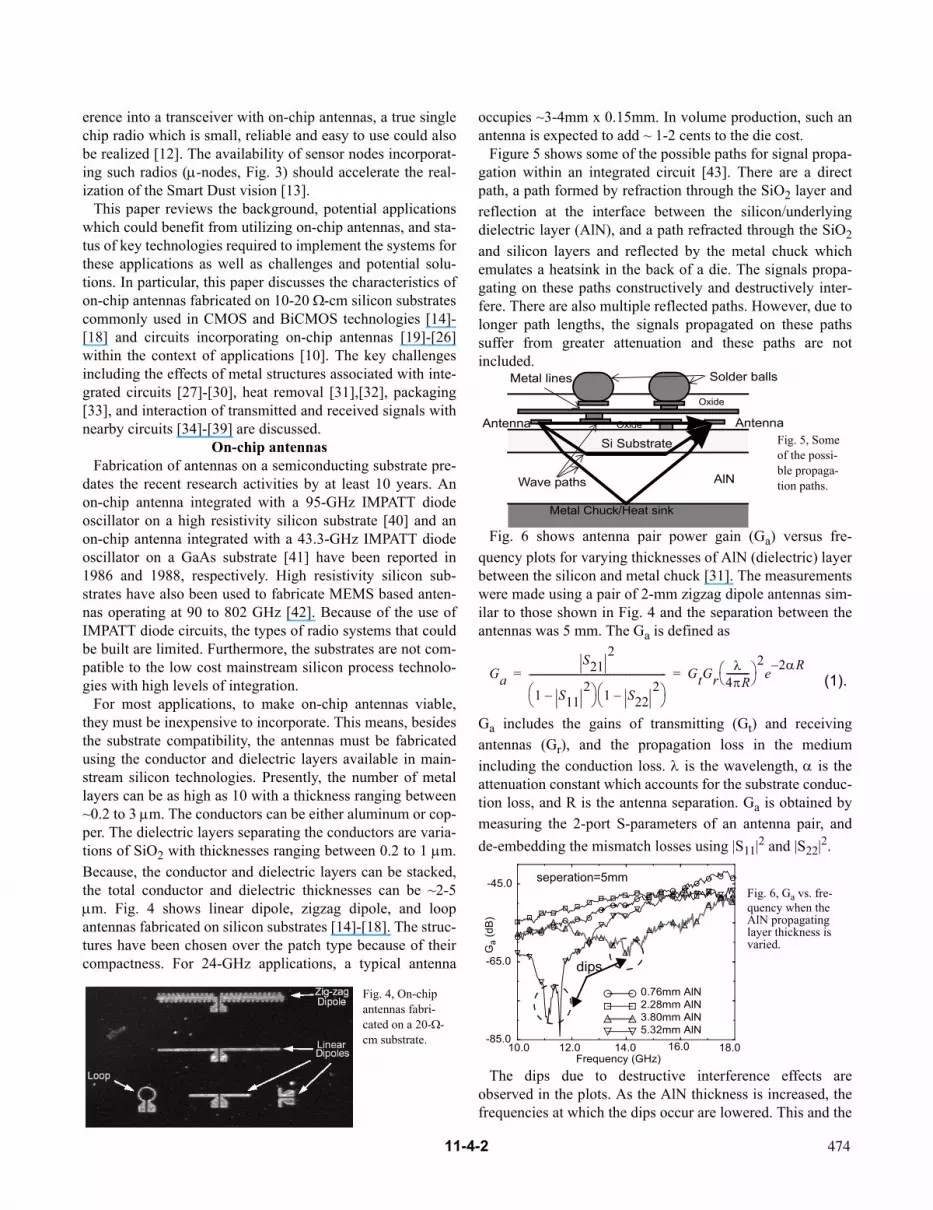
Figure 5 shows some of the possible paths for signal propa-gation within an integrated circuit [43]. There are a directpath, a path formed by refraction through the SiO2 layer andreflection at the interface between the silicon/underlyingdielectric layer (AlN), and a path refracted through the SiO2and silicon layers and reflected by the metal chuck whichemulates a heatsink in the back of a die. The signals propa-gating on these paths constructively and destructively inter-fere. There are also multiple reflected paths. However, due tolonger path lengths, the signals propagated on these pathssuffer from greater attenuation and these paths are notincluded.
Fig. 6 shows antenna pair power gain (Ga) versus fre-quency plots for varying thicknesses of AlN (dielectric) layerbetween the silicon and metal chuck [31]. The measurementswere made using a pair of 2-mm zigzag dipole antennas sim-ilar to those shown in Fig. 4 and the separation between theantennas was 5 mm. The Ga is defined as
Ga includes the gains of transmitting (Gt) and receivingantennas (Gr), and the propagation loss in the mediumincluding the conduction loss. λ is the wavelength, α is theattenuation constant which accounts for the substrate conduc-tion loss, and R is the antenna separation. Ga is obtained bymeasuring the 2-port S-parameters of an antenna pair, andde-embedding the mismatch losses using |S11|2 and |S22|2.
The dips due to destructive interference effects areobserved in the plots. As the AlN thickness is increased, thefrequencies at which the dips occur are lowered. This and the
Fig. 4, On-chip antennas fabri-cated on a 20-Ω-cm substrate.
Fig. 5, Some of the possi-ble propaga-tion paths.
Metal lines Solder balls
AlNWave paths
Antenna Antenna
Si Substrate
Oxide
Oxide
Metal Chuck/Heat sink
GaS21
2
1 S112–
1 S222–
------------------------------------------------------------ GtGr
λ4πR----------
2e 2αR–= = (1).
Frequency (GHz)
0.76mm AlN2.28mm AlN3.80mm AlN5.32mm AlN
seperation=5mm
10.0 12.0 14.0 16.0 18.0-85.0
-65.0
-45.0
dips
Ga
(dB
)
Fig. 6, Ga vs. fre-quency when the AlN propagating layer thickness is varied.
47411-4-2

fact that Ga improves when the substrate is made insulating[14],[15] are clear indications that the signal transmissionand reception are via wave propagation. The addition of a0.76-mm thick AlN layer improves the gain by around ~10dB compared to the case when the wafer is in direct contactwith the metal chuck. The AlN layer has a thermal conduc-tivity comparable to Al and provides an excellent thermalpath for heat removal. Fig. 7 shows the radiation patterns ofdipole and loop antennas at 10 GHz, which are consistent tothat expected from the basic antenna theory.
Intra-chip global signal distribution.On-chip antennas and transceivers can be used to distrib-
ute global control signals such as clock, SLEEP andRESET. In fact, clock distribution was used to drive the ini-tial development of on-chip antennas. In the wirelessapproach, the clock is transmitted using a monotone sinewave and the received signal is amplified, divided and buff-ered to provide local clock signals (Fig. 1). At the 0.18-µmgeneration, the latency for wireless clock distribution sys-tem was estimated to be around ~400pS compared to ~ 1nSof conventional clock distribution networks. The latenciesto all points in a chip must be matched to a tighter tolerancewith each succeeding technology generation to facilitate theincrease of clock frequency. The latencies in wireless sys-tems are dominated by the delay through clock receiver cir-cuits and this delay scales down with technology as shownin Fig. 8, while the latency for conventional system isexpected to remain essentially constant. This means for con-ventional clock distribution systems, the latencies must bematched to a smaller percent of the total latency compared
to a wireless clock distribution network. Furthermore, forthe wireless approach, the clock drivers are distributed overa chip (Fig. 1). This should reduce the temperature variationin the chip, which is a significant source of skew. These arefundamental distinctions that could lead to smaller skew fora wireless clock distribution system. In addition, since a sin-gle tone sine wave is used for clock transmission, the prob-lems due to dispersion which could ultimately limit the chipsize and clock [44] is effectively eliminated. The sine wavebased clock distribution can also be used in wiredapproaches to solve the dispersion problem.
On wafer, a 15-GHz transmitted signal 2.2 cm away froma clock receiver with an on-chip antenna has been success-fully picked up by the receiver and amplified to generate adigital output signal [31] (Fig. 9). The receiver and transmit-ter were fabricated using a 0.18-µm CMOS process [20].Fig. 10 shows micro-photographs of the transmitter andreceiver. The receiver area including the antenna is 5.86 x105 µm2. The area excluding bond pads is 3.75 x 10⁵ (~ 600x 600 µm2). The receiver consumes 40 mW of power. Thetransmitter consists of a voltage controlled oscillator, anamplifier, and an antenna. The transmitter occupies an areaof ~600x400 µm2 excluding the bond pads, and consumes50 mW of power. For the clock application, transmissionover 2.2 cm is sufficient for the largest chip projected by the2005 ITRS [6].
The measured peak-to-peak receiver jitter is 6.6 ps at1.875 GHz, corresponding to 1.24% of a local clock period[20]. While, this is promising, additional measurements inmore realistic digital IC configurations are necessary. The
-10dB
-5dB
0dB
30
210
60
240
90
270
120
300
150
330
180 0
linearzigzag
-40dB
-20dB
0dB
30
210
60
240
90
270
120
300
150
330
180 0
Loop AntennaDipole Antenna
Fig 7, radiation patterns of dipole and loop antennas.
0.0
500
1000
1500
2000
1997 1999 2001 2003 2005 2007 2009Year
0.0
200
400
600
Chi
p Si
ze (m
m2 )
0.0
500
1000
1500
2000
0.0
500
1000
1500
200
Latency (pSec)
Wireless ClockConventional ClockSkew ToleranceChip Size
Fig. 8, Latencies versus time for clock distribution systems.
-0.05
0.15
0.35
-0.4
0.0
0.4fin=16 GHz fout=2 GHz
SignalGenerator
AmplifierBalun &SS Probe
Clock Receiver
GSSGProbe Oscilloscope
Inpu
t Sig
nal (
V)
Out
put S
igna
l(V)
Time (ns)Time (ns) 1.0ns 1.0ns
Fig. 9, Transmitted and the digital output signal of a clock receiver 2.2 cm away from a transmitting antenna.
Fig. 10, A transmitterand receiverpair fab-ricated in the UMC 0.18-µmCMOSprocess.
Transmitter
Receiver
47511-4-3

power consumption of a wireless clock distribution systemusing 16 receivers over the areas projected by the ITRS hasbeen estimated and found to be comparable to that of conven-tional systems [45],[46]. This is due to the fact that most of thepower consumption of a clock distribution network isexpended for driving local loads.
Metal structures near antennas can change the input imped-ance and phase of received signals. To deal with this, designguidelines to exclude the interference structures which signifi-cantly change the input impedance are being developed.[29],[30]. Additionally, a technique for correcting delay varia-tions using a frequency divide-by-8 circuit with 16-program-mable steps has been demonstrated [47].
Fig. 11 shows a block diagram of a wireless clock distribu-tion system including a clock transmitter and a receiver thatcontains a divider with programmable delays. The transmittedclock has ~1.5nS of no transmission. The receiver uses this togenerate an initialization pulse and to equalize the varyingdelays. Fig. 11 also shows that the receiver outputs can beshifted by applying varying program codes.
Another concern is the interference effects between transmit-ted signal and nearby circuits [34],[35], and between the trans-mitted/received signal and switching noise of nearby circuits[36]-[39]. EIRP (effective isotropic radiated power) up to ~40dBm had almost negligible impact on operation of 16-MbitDRAM’s [34] and 10-bit pipelined A/D converters [35]. A925-MHz output signal derived from a 7.4 GHz wireless inter-connect [19] was used to drive 100-stage inverter chains (Fig.12). This was the first use of a wireless interconnect to drivedigital circuits. As the number of inverter chains turned on isincreased, the resulting switching noise increases the jitter of
received signal and ultimately, disrupts the receiver operation.The cause for this is the changes of the receiver amplifier gainand self-oscillation frequencies of the frequency divider due tothe substrate noise injected from the switching inverters. Theoperation was restored by increasing the transmitted power tocompensate for the gain reduction and by re-centering the self-oscillation frequency of the divider [39]. It should be possibleto reduce the sensitivity to the substrate injected noise byusing guard rings and by isolating the body nodes of NMOStransistors in clock receivers using a triple n-well processwhich is starting to be widely available.
The characteristics of on-chip antennas are expected to bestrongly influenced by packaging, and dealing with this hasbeen considered as a major challenge. The chips including thereceiver and transmitter shown in Fig. 10 were housed in 407-pin flip-chip packages with a ball grid array (BGA), and testedon a printed circuit (PC) board (Fig. 13) [33]. The relativepermittivity of underfill is 3.2. The package is 16 mm x 16 mmwith two metal layers. The PCB contains four metal layers, andthe dielectric is FR4.
VCO
ControlCircuit
LNAProgrammable
Detector INIProgrammed delayBuffer
starting point
Divider (1/8)
P1 P2 P3 P4
0.0 0.2 0.4 0.6 0.8 1.0-0.20
0.00
0.20
0.40
0.60
0.80
Am
plitu
de (V
)
1000
0100
0010 0001 0000
Time (ns)
(P4P3P2P1) 0001 0010 0100 1000
Expected (ps) 222 111 55.5 27.5Measured (ps) 220 109 55 24
Fig. 11, Block diagrams for clock transmitter and receiver with a programmable divider. Output waveforms of a receiver.
~1.5ns no transmission
InverterChains
InverterChains
8:1 Divider
Multiplexer,Oscillator,Control & Buffers
TxAntenna
200µm
Fig. 12, A 7.4-GHz clock receiver surrounded by inverter chain driven by the receiver.
Fig. 13, The transmitter and receiver shown in Fig. 10 were housed in a flip-chip package with aball grid array. The chipwas tested in a printedcircuit board.
47611-4-4

Using this, a sine wave generated in a transmitter wastransmitted through an on-chip antenna and the wave waspicked up by a receiver in the same chip ~4 mm away. Theseparation was limited by the size of chip. The testing requiresonly dc connections to the receiver and transmitter except theoutput connections for the receiver. The output similar to thatshown in Fig. 9 has been obtained clearly indicating that on-chip wireless interconnects function even inside a package.
Presently, the antennas and circuits are too big and their useis restricted. However, as the maximum operating frequency ofCMOS circuits is increased with the scaling, the antenna andcircuit sizes are expected to decrease. As a matter of fact, aclock receiver operating around 200 GHz (Year 2015) isexpected to occupy an area of ~100 x 200 µm2. At suchdimensions, there will be much greater flexibility for their use.
Clock distribution using an external antennaA clock distribution system with an external planar array
antenna is shown in Fig. 14. The form factor of this systemcould be comparable to that of conventional systems used indesk-top computers. A signal-signal probe acting as a receiv-ing antenna was used to map the power and phase distributionsfrom the off-chip 24-GHz planar array antenna in Fig. 14. Theantenna bandwidth is 2GHz. For the case without a heatsink,the gains range between -54 to -61dB (Fig. 15(a)), and phasesrange between -591 to -658 degree (Fig. 15(b)) over a circulararea with a diameter of 35mm. When the signal is divideddown to 3GHz, the phase variation will translate to a clockskew of 2.3% of a period. The gain variation also adds toskew. Receiver simulations indicate that 10-dB gain variationinduces skew less than 1.0% of a period [47]. The total skewshould be less than 3% or ~10pS, which is significantly lessthan the typical skew/jitter tolerance of 10% of a period. Simi-lar skew has been observed even in the presence of a heatsink[32],[48]. The area is ~4X larger than that typically thoughtpossible for synchronization at ~3GHz.
A prototype system including an initialization scheme tosynchronize distributed clock receivers has been demonstratedin the UMC 130-nm CMOS process [48]. Based on the mea-surements and simulations of the prototype, the skew includ-ing the effects of temperature and process variations isexpected to be less than ~20pS over the area with a diameter
of 35mm. Furthermore, the receiving antennas can be as smallas a pair of bond pads even for a system operating at 24 GHz[32], and could make this approach more practical in nearerterm than the intra-chip clock distribution.
Intra-chip and inter-chip data communicationThe on-chip antennas can also be used for data
communication [9],[49]. The packaging costs not following thesilicon die cost reduction curve has been cited as a difficultchallenge facing the silicon IC industry beyond 2010 [6]. Toalleviate this problem, the input/output (I/O) pins could bereplaced with wireless connections formed using transmittersand receivers with on-chip antennas. Transient characteristicsof antennas [49] as well as fractal antennas [50] with ultra wideband matching have been investigated for this purpose. Eachreceiver and transmitter pair can replace multiple pins by use ofmultiple access techniques such as frequency division multipleaccess, code division multiple access and others [51]. Thisdecrease of number of pins reduces the foot prints of packagedIC’s as illustrated in Fig. 2. This should also decrease the delaysbetween pins. This delay reduction however, must be balancedby the added delays of transmitter and receiver. The wirelessdata communication can also provide additional capabilitiessuch as communication by more than one pair of devices at thesame time.
Planar-array antenna
Heatsink
PC board with IC
Fig. 14. A compact clock distribution system using an external planar array antenna. A fan could be placed on the sides. A heatsink with aper-tures (1.5mm x 7 mm).
6mm
3cm
A B C
(b)
(a)
Fig. 15, (a) Relative gain (dB) distribution, and (b) phase (degree) distribu-tion across a 4-inch-diameter opening illuminated with a planar array
47711-4-5

The two main concerns for inter-chip and intra-chip wirelessdata communication are bandwidth and power consumption.The bandwidth is limited by the maximum operating frequencyof RF circuits. As discussed, by 2015, RF circuits operating upto ~250 GHz could be fabricated in CMOS technologies. Thisseemingly high operating frequency by itself will most likelynot be sufficient to support the required bandwidth for intra-chip and inter-chip data communications. The typicalbandwidth efficiency of ~1 bit-sec-1-Hz-1 leads to a data rate ofonly ~250 Gbits/sec. To overcome this, cellular datacommunication much like that used for cellular phones couldbe utilized. For instance, if the space around a chip can bedivided into 10 cells, this could increase the aggregate data rateto ~2.5 Tbits/sec, which should probably be sufficient for theinter-chip applications in 2015.
For general purpose intra-chip global data communication,the ~2.5-Tbits/sec data rate is still unacceptably low. Asmentioned, this does not preclude the use of on-chip wirelessinterconnects for distributing global control signals such asRESET and SLEEP as well as for specialized global andintermediate data communication with moderate data rates. Fordistributing control signals, it may be possible to share theantennas and parts of the clock receiver circuitry to reduce theoverhead.
General purpose communicationOn-chip antennas can also be used for general purpose
communication over air. Integration of antennas is one of thekey technologies which should someday enable realization of atrue single chip radio [10],[12],[22]. Inclusion of compactantennas in an integrated circuit reduces the radio size, greatlysimplifies its use, reduces assembly cost, and eliminates theneed for external transmission line connections andsophisticated packaging, which should radically reduce thecost of wireless systems operating above 10GHz. Atfrequencies higher than 100GHz, the only practical approachfor getting signals in and out of an IC may be to use on-chipantennas. Presently, a 24-GHz version for short range (1-5m)communication is being developed using 130-nm CMOS
technology. This true single chip radio called µNode willsupport a data rate of 100kbits/sec.
Figure 16 shows Ga versus antenna separation plots for thisapplication. The antennas are fabricated on 20-Ω-cm siliconsubstrates and thinned to 100µm. Ga’s decrease as theseparation is increased with slope of -2 up to 1-2 m separations.At larger separations, the plots deviate from this due to themultiple path effects. Ga’s are strongly dependent on the heightfrom the ground. Presently, the best reported efficiency for on-chip dipole antennas is ~ 15-20%, which has been achieved bythinning the silicon substrate to 100 µm. Since the wavepropagation in this application is mostly through air and thesubstrate can potentially be much more drastically thinned, theefficiency should ultimately be limited by the metal thicknessesavailable in integrated circuits. The efficiency shouldeventually be increased to above 70%. The link analysis givenin Table 1 suggests that an antenna pair gain of ~-94 dB will besufficient to build a radio link. This means that when antennasare located at 52-cm from the ground, the antennas areadequate for communication up to ~10m.
As an initial feasibility study for the single chip radio, a 24-GHz down converter (Fig. 17) consisting of a differential lownoise amplifier, a double balanced gilbert cell mixer, and an on-chip antenna has been fabricated using the UMC 130-nmdigital CMOS process. At VDD=1.2V, the circuit has maximumpower gain of 7dB, minimum NF of 7.2dB and the total powerconsumption of 7.3mW. This is adequate to satisfy the 8-dBreceiver noise figure target, if the down converter is followedby an intermediate frequency (IF) amplifier with gain and noisefigure of 25 dB and 2.5 dB.
6mm
Fig. 16, A 6-mm monopole antenna with 600-µm long sleeve. Ga versusseparation plots for monopole and dipole antennas. The antennas are located
0.1 1 10Distance (m)
-100.0
-90.0
-80.0
-70.0
-60.0
-50.0
-40.0
-30.0G
a (d
B)
Theoretical Monopole at 5.8 GHzThin monopole at 52 cmThin dipole at 52 cm
30
5.8 GHz24 GHz
52 cm above the ground.
Table 1: Link margin analysis for µNodes.
TX Power 10 dBmPropagation and Antenna Loss 94 dB Received Power -84 dBmThermal Noise -173.8 dBm/HzBandwidth (100 kBits/sec) 50 dBEb/No 18 dBRX noise figure 8 dBSensitivity -97.8 dBmLink Margin 13.8 dB
Ld3
Ld4
Lg1 Lg2
Ld1 Ld2
L1
L2
L3
RF+ RF-
LO+ LO-
IF+
IF-
LNA
Mixer
Pad
Vias
From metal 1 to metal 4 layer.
Feed-line (Top Metal
layer).
Ld3
Ld4
Lg1 Lg2
Ld1 Ld2
L1
L2
L3
RF+ RF-
LO+ LO-
IF+
IF-
LNA
Mixer
Pad
Vias
From metal 1 to metal 4 layer.
Feed-line (Top Metal
layer).
Fig. 17, A 20-GHz down-converter fabricated in 130-nm CMOS.
47811-4-6

Communication over air using the down converter wasdemonstrated by transmission of an AM signal utilizing an on-chip antenna, and reception and down conversion of this signalto IF utilizing the down-converter. The measurement setup isshown in Fig. 18. The transmitted signal was generated by anAgilent 8254A. The carrier frequency was 20GHz and themodulating signal was 100kHz with a modulation depth of50%. The signal was converted to balanced using a balun andfed to a 3-mm on-chip zigzag dipole antenna with a signal-signal probe. The power delivered to the antenna was 10dBm.The antenna was placed on a Derlin mobile probe stand [16].The receiver was located 5m away. The IF output wasamplified using an external amplifier with 26-dB gain. Thereceived spectrum at a resolution bandwidth of 300Hz is shownin Fig. 18. The power at 3-GHz IF was –53.8dBm. The two sidebands 100kHz away have power levels of 12.7 and 12.2dBlower than that for the carrier, which are close to the theoreticalvalue.
The 5-m range of a single chip radio using on-chip antennasis indeed a pleasant surprise. However, the 5-m range is still alimitation. In order to increase the range, use of on-chipantennas at 5.8 GHz has been investigated. In particular, tokeep the antenna small, monopole antennas which ideally act asdipole antennas with twice the length have been investigated.Fig. 16 also compares Ga’s of the monopole with a 600-µmlong sleeve which acts like a ground plane to the previouslyreported on-chip dipole results at 24GHz [18]. When theantennas are located at 52cm from the ground, Ga of 6-mmmonopole pair at 5.8GHz is ~10dB higher than that for the 3-
mm dipole pair at 24GHz. Since λ at 5.8GHz is 4X longer thanthat at 24GHz, Ga at 5.8GHz is 12dB higher (Eq. 1) if the gainsof transmitting and receiving antennas (Gt and Gr) areunchanged. These indicate that the efficiency of monopoles issimilar to that (15~20%) for the previous reported dipoles [17].
Once again, assuming that -94-dB Ga is adequate for a radiolink, a range of ~30m should be achievable using the mono-poles that are only ~30% larger than that for the dipoles usedat 24-GHz. This is an increase in communication range of~3X. This work has shown that not only it is practical to inte-grate compact antennas for operation at 5.8GHz, but also it ispreferred due to the increase of communication range.
ConclusionsOn-chip antennas can be used to communicate within and
between IC’s. Signals propagate at the speed of light of a prop-agation medium [14], but the wireless interconnects using on-chip antennas do not require optical components that are diffi-cult to integrate [52]. As the maximum operating frequency ofCMOS circuits increases with technology scaling, the requiredantenna and circuit areas will scale down. This will reduce thecost of on-chip wireless interconnects and greatly increase theflexibility for use of on-chip antennas. Besides the uses inintra-chip and inter-chip wireless interconnections, and truesingle chip radios, on-chip antennas can be used for manyother applications. They could be used in beacons [21],[23],radars [10],[24], RFID’s [53],[54], rectennas [39], as well as incontact-less high frequency testing [55],[56].
AcknowledgementsThis work is supported by SRC (Task ID: 453 and 885),
DARPA (N66001-03-1-8901), NASA (NAG10-316 andNAG3-2930), and NSF (0424335).
References[1] B.-A. Floyd and K. K. O, “A 23.8-GHz SOI CMOS Tuned Amplifier,”IEEE Trans. on Microwave Theory and Techniques, vol. 50, issue 9, pp. 2193-2196, Sep. 2002.[2] C.-M. Hung, L. Shi, I. Lagnado, and K. K. O, “A 25.9-GHz Voltage-Con-trolled Oscillator Fabricated in a CMOS Process,” 2000 VLSI Symposium onCircuits, pp. 100 - 101, Honolulu, HI, June 2000.[3] L. M. Franca-Neto, R. Bishop, and B. Bloechel, “64 GHz and 100 GHzVCO’s in 90 nm Using Optimum Pumping Method,” 2004 InternationalSolid-State Circuits Conference, pp. 444-445, Feb. 2003, San Francisco, CA.[4] M. Wetzel et al., “A 26.5-GHz Silicon MOSFET 2:1 dynamic frequencydivider,” IEEE Microwave and Guide Wave Letts, vol. 10, no. 10, pp. 421-423, Oct. 2000.[5] C. H. Doan et al., “Millimeter-Wave CMOS Design,” IEEE J. of Solid-State Circuits, vol. 40, no. 1, pp. 144-155, Jan. 2005.[6] 2005 International Technology Roadmap for Semiconductors, SIA[7] C. Cao and K. K. O, “192-GHz Push-push VCO in 0.13-µm CMOS” IEEElectronics Letters, vol. 42, no. 4, pp. 208-210, Feb. 2006.[8] E. Seok, C. Cao, S. Sankaran, and K. K. O, “A Millimeter-Wave SchottkyDiode Detector in 130-nm CMOS Technology,” Accepted to 2006 Sympo-sium on VLSI Circuits.[9] K. K. O et al., “Inter and Intra-Chip Wireless Clock Signal DistributionUsing Microwaves: A Status of an Initial Feasibility Study,” Gov. Microcir-cuit Applications Conference, pp. 306-309, Mar. 1999, Monterey, CA.[10] K. K. O et al., “On-chip Antennas in Silicon IC’s and Their Apps.,” IEEETrans. on Elec. Dev., vol. 52, no. 7, pp 1312-1323, July, 2005.[11] Q. Shi, R. J. O’Dea, and F. Martin, “A new chip-level differential detec-tion system for DS-CDMA,” IEEE International Conference on Communica-
-130
-110
-90
-70
-50
-30
2.9995 3 3.0005
Frequency (GHz)
dBm
-53.8dBm
-66dBm-66.5dBm
-130
-110
-90
-70
-50
-30
2.9995 3 3.0005
Frequency (GHz)
dBm
-53.8dBm
-66dBm-66.5dBm
Receiver
TransmittingAntenna
5m
LOIFDC
Chip
Receiver
TransmittingAntenna
5m
LOIFDC
Chip
Fig. 18, A setupto transmit 20-GHz10-dBm AM modulated signals
using an on-chipantenna, and toreceive thesignals using thedown converterin Fig. 17.
47911-4-7

tions, vol. 1, pp. 544-547, April 2002.[12] K. K. O, J. E. Brewer, and D. Taubenheim, “RF Subsystem for µNodeSOC,” 2005 GOMAC, Paper 9.5, Las Vegas, NV, April, 2005.[13] B. Warneke et al., “Smart Dust: communicating with a cubic-millimetercomputer,” Computer, vol. 34, no. 1, pp. 44-51, Jan. 2001.[14] K. Kim and K. K. O, “Characteristics of Integrated Dipole Antennas onBulk, SOI, and SOS Substrates for Wireless Communication,” Proceedings ofthe Intl. Interconnect Conference, pp 21-23, San Francisco, CA, June 1998.[15] K. Kim. H. Yoon, and K. K. O, “On-Chip Wireless Interconnection withIntegrated Antennas,” IEDM, pp. 485-488, Dec. 2000, San Francisco, CA.[16] J. J. Lin et al., “Integrated Antennas on Silicon Subst. for Comm. overFree Space,” IEEE Elec. Dev. Letts., vol. 25, no. 4, pp 196-198, April, 2004.[17] J.-J. Lin et al., “10x Improvement of Power Transmission over FreeSpace Using Integrated Antennas on Silicon Substrates,” 2004 Custom Inte-grated Circuits Conference, pp. 697-700, Oct. 2004, Orlando FL.[18] J.-J. Lin, H.-T. Wu, and K. K. O, “Compact On-Chip Monopole Antennason 20-Ω-cm Silicon Substrates for Operation in the 5.8-GHz ISM Band,” 2005IEDM, pp. 967-970, Dec. 2005, Washington, DC.[19] B. A. Floyd, K. Kim, and K. K. O, “Wireless Interconnection in a CMOSIC with Integrated Antennas,” Tech. Digest of 2000 IEEE International Solid-State Circuits Conference, pp. 328-329, Feb. 2000, San Francisco, CA.[20] B. A. Floyd, C.-M. Hung, and K. K. O, “15-GHz Wireless InterconnectImplemented in a 0.18-µm CMOS Technology Using Integrated Transmitters,Receivers, and Antennas,” IEEE J. of Solid-State Circuits, vol. 37, no. 5, pp.543-552, May 2002.[21] F. Touati and M. Pons, “On-chip integration of dipole and VCO usingstandard BiCMOS technology for 10 GHz applications,” 2003 EuropeanSolid-State Circuits Conference, pp. 494-497, October 2003.[22] Y. Su, J.-J. Lin, and K. K. O, “A 20-GHz CMOS RF Down-Converterwith an On-chip Antenna,” 2005 Intl. Solid-State Circuits Conference, pp.270-271, Feb. 2005, San Francisco, CA.[23] T. Al-Attar and T. H. Lee, “Monolithic Integrated Millimeter-WaveIMPATT Transmitter in Standard CMOS Technology,” IEEE Trans. on Micro-wave Theory and Techniques, vol. 53, no. 11, pp. 3557-3561, Nov. 2005.[24] A. Babakhani et al., “A 77-GHz 4-Element Phase Array Receiver withOn-chip Dipole Antenna in Silicon,” 2006 International Solid-State CircuitsConference, pp. 180-181, Feb. 2006, San Francisco, CA.[25] C.-H. Wang et al., “A 60GHz Transmitter with Integrated Antenna in0.18µm SiGe BiCMOS Technology,” 2006 International Solid-State CircuitsConference, pp. 186-187, Feb. 2006, San Francisco, CA.[26] C. Cao et al., “A 24-GHz Transmitter with on-chip antenna in 130-nmCMOS,” Accepted to 2006 Symposium on VLSI Circuits.[27] H. Yoon, K. Kim, and K. K. O, “Interference Effects on Integrated DipoleAntennas by a Metal Cover for an Integrated Circuit Package,” 2000 IEEEAP-S International Symposium and USNC/URSI National Radio ScienceMeeting, pp. 782- 785, July 2000, Salt Lake City, UT.[28] A. B. M. H. Rashid et al., “Interference Suppression of Wireless Intercon-nection in Si Integrated Antenna,” 2002 International Interconnect Confer-ence, pp. 173-175, June 2002, San Francisco, CA.[29] X. Guo et al., “Design Guidelines for Reducing the Impact of Metal Inter-ference Structures on the Performance On-chip Antennas,” 2003 IEEE AP-SIntl. Symp. and USNC/URSI NRSM, Vol. 1, pp 606-609, June, 2003.[30] E.-Y. Seok and K. O, “Design Rules for Improving Predictability of On-chip Antenna Characteristics in the Presence of Other Metal Structures,” 2005Intl. Interconnect Tech. Conf., pp. 120-123, San Francisco, CA, June 2005.[31] X. Guo, J. Caserta, R. Li, B. Floyd, and K. K. O, “Propagation Layers forIntra-Chip Wireless Interconnection Compatible with Packaging and HeatRemoval,” 2002 Symp. on VLSI Tech., pp. 36-37, June, 2002, Honolulu, HI.[32] R. Li, X. Guo, and K. K. O, “A Technique for Incorporation of a Heatsinkfor a System Utilizing Integrated,” 2004 International Interconnect Technol-ogy Conference, pp. 160-162, June 2004, San Francisco, CA.[33] J. Branch, X. Guo, L. Gao, A. Sugavanam, J.-J. Lin, and K. K. O, “Wire-less Comm. in a Flip-Chip Package using Integrated Antennas on Silicon Sub-strates,” IEEE Elec. Dev. Letts., vol. 26, no. 2, pp 115-117, Feb. 2005.[34] J. Bohorquez and K. K. O, “A Study of the Effects of Microwave Electro-
magnetic Radiation on Dynamic Random Access Memory Operation,” 2004IEEE Intl. Symp. on EMC, vol. 3, pp. 815-819, Aug. 2004, San Jose, CA. [35] M. Hwang and K. K. O, “A Study of the Impact of Microwave Radiationon an A/D Converter,” 2004 IEEE Intl. Symp. on EMC, vol. 2, pp. 307-311,Aug. 2005.[36] J. Mehta, and K. K. O, “Switching Noise of Integrated Circuits (IC’s)Picked up by a Planar Dipole Antenna Mounted Near the IC’s,” IEEE Trans.on Electro-Magnetic Compatibility, vol. 44, no. 5, pp. 282-290, May 2002.[37] D. Bravo, H. Yoon, K. Kim, B. Floyd, and K. K. O, “Estimation of theSignal-to-Noise Ratio for On-Chip Wireless Clock Signal,” 2000 Intl. Inter-connect Technology Conference, pp. 9 - 11, June 2000, San Francisco, CA.[38] T. O. Dickson, D. Bravo, and K. O, “Noise Coupling to On-Chip Anten-nas,” 2002 IEEE Intl. Symp. on EMC, vol.1, pp. 340-344, Minneapolis, MN.[39] T. O. Dickson, B. Floyd, and K. K. O, “Jitter in a Wireless Clock Distri-bution System,” 2002 International Interconnect Technology Conference, pp.154-156, June 2002, San Francisco, CA.[40] J. Buechler et al., “Silicon High-Resistivity-Substrate Millimeter-WaveTech.,” IEEE Trans. on MTTS, vol. mtt-34, no. 12, pp. 1516-1521, Dec. 1986.[41] N. Camilleri and B. Bayraktaroglu, “Monolithic Millimeter-WaveIMPATT Oscillator and Active Antenna,” 1988 IEEE MTT-S Digest, pp. 955-958, June 1988.[42] G. Rebeiz et al., “Integrated Horn Antenna for Millimeter-Wave Apps.,”IEEE Antennas and Prop. Magazine, vol. 34, no. 1, pp. 7-16, Feb. 1992.[43] K. Kim, W. Bomstad, and K. K. O, “A Plane Wave Model Approach toUnderstanding Propagation in an Intra-chip Communication System,” 2001IEEE AP-S International Symposium and USNC/URSI National Radio Sci-ence Meeting, vol. 2, pp. 166-169, Boston, MA.[44] A. Deutsch et al., “Functional high-speed characterization and modelingof a six-layer copper wiring structure and performance comparison with alu-minum on-chip interconnections,” Tech. Digest of IEEE International Elec-tron Devices Meeting, pp.295-298, Dec. 1998, San Francisco, CA.[45] B. A. Floyd, and K. K. O, “The Projected Power Consumption of a Wire-less Clock Distribution System and Comparison to Conventional Systems,”Proceedings of the 1999 IITC, pp. 248-251, June 1999, San Francisco, CA.[46] K.-N. Chen, M. Kobrinsky, B. Barnett, and R. Reif, “Comparisons ofconventional, 3-D, optical, and RF-interconnects for on-chip clock distribu-tion,” IEEE Trans. on Electron Dev., vol. 51, no. 2, pp. 233-239, Feb. 2004.[47] X. Guo, D.-J. Yang, K. K. O, “A Receiver with Start-up Initialization andProgrammable Delays for Wireless Clock Distribution,” 2006 InternationalSolid-State Circuits Conference, pp. 386-387, Feb. 2006, San Francisco, CA.[48] R. Li, X. Guo, D.-J. Yang, K.K. O, “Initialization of a wireless clock dis-tribution system using an external antenna,” IEEE Conf. Custom IntegratedCircuits, pp. 105-108, September 2005, San Jose, CA.[49] S. Watanabe, K. Kimoto and T. Kikkawa, “Transient Characteristics ofIntegrated Dipole Antennas on Silicon for Ultra Wideband Wireless Intercon-nects,” 2004 IEEE AP-S Intl. Symp. and USNC/URSI NRSM, paper 84.4,July 2004, Monterey, CA.[50] K. Kimoto et al., “Characteristics of Fractal Dipole Antennas Integratedon Si for ULSI Wireless Interconnects,” 2004 IEEE AP-S Intl. Symp. andUSNC/URSI NRSM, paper 121.5, July 2004, Monterey, CA.[51] M. F. Chang et al., “RF/wireless interconnect for inter- and intra-chipcommunication,” Proc. of IEEE, vol. 89, no. 4, pp 456-466, April 2001.[52] D. A. B. Miller, “Rationale and challenges for optical interconnects toelectronic chip,” Proc. of the IEEE, vol. 88, no. 6, pp. 728-749, June 2000.[53] J. Bouvier, Y. Thorigne, S. A. Hassan, M. Beviliet, and P. Senn, “A SmartCard CMOS Circuit with Magnetic Power and Communications Interface,”1997 Intl. Solid-State Circ. Conf., pp. 296-297, Feb. 1997, San Francisco, CA.[54] M. Usami et al., “Powder LSI: An Ultra Small RF Identification Chip forIndividual Recognition Applications,” Tech. Digest of 2003 InternationalSolid-State Circuits Conference, pp. 444-445, Feb. 2003, San Francisco, CA.[55] B. Moore, M. Margala, and C. Backhouse, “Design of wireless on-wafersubmicron characterization system,” IEEE Trans. on VLSI Systems, vol. 13,no. 2, pp. 169-180, Feb. 2005.[56] W. Yin and W. R. Eisenstadt, “Wireless Signal Generation for RF ICEmbedded Test,” WTW2005, 4th Workshop on Test of Wireless Circuits andSystems, pp. 5, June 2005, Cannes France.
48011-4-8


