Embed Size (px)
Citation preview

©2016, IJCERT All Rights Reserved DOI:10.22362/ijcert/2016/v3/i10/48905 Page | 554
Volume 3, Issue 10, October-2016, pp. 554-560 ISSN (O): 2349-7084
International Journal of Computer Engineering In Research Trends
Design of DC-DC Boost Converter in CMOS
0.18µm Technology
1M.RAMA DEVI,
2 R.SUNIL KUMAR,
3M.MADHAVA KUMAR
1M.Tech scholar 2Asst.professor, Dept of Electronics and communication Engineering,
Gayatri Vidya Parishad College of Engineering for Women, Visakhapatnam, Andhra Pradesh, India. 3 DRDO Scientist-F ANURAG Laboratories, Hyderabad, India.
[email protected],[email protected]
Abstract -A CMOS DC-DC boost converter with fastest settling time and less quiescent current with a feedback control
is implemented. An extra path is introduced because of an error amplifier (OTA) which has an effective control for fast
response. Efficient compensation with soft-start is used to make the quiescent current low. An on-chip current sensing
circuit is introduced with less number of I/O pins for current mode control. In this project, the DC-DC boost converter is
designed in Cadence virtuoso 0.18µm technology with a 5V supply. With a wide range of loads, it provides 25V at the
output, 50mA load current with 90% efficiency. The circuit is operated at 500 KHz clock frequency with output ripple
voltage of 20mV by using 4.7µF off-chip capacitor and 75µH off-chip inductor.
Key words—DC-DC Boost converter, operational Tran’s conductance amplifier (OTA), comparator, pulse width
generator, compensator, current sensing circuit, oscillator and ramp generator circuit.
————————————————————
I. INTRODUCTION
The power management system is the most
important part of an IC in the modern technology.
Especially developments in the portable devices
which operate with batteries are more dependent
on the power supply. Since, these are having
modules operated with different voltage supplies;
DC-DC converters play a major role in the power
management systems. These circuits are designed to
provide stable power supply to guarantee the
operation. Moreover, DC-DC converters take
unregulated DC voltage as input and produce a
constant or regulated voltage as an output. Due to
this requirement, voltage regulators have become
common place in Integrated circuits. These
regulators are basically two types, linear and
switching regulators. All types of regulators have
power stage followed by the control circuitry to
sense the feedback signals that adjusts the power
stage to maintain the regulated output voltage. To
maintain regulation and system stability the DC-DC
converter consists of a controller with a feedback
loop and a compensation circuit respectively.
II. DC-DC BOOST CONVERTER
Fig 1: Block diagram of boost converter
Available online at: www.ijcert.org

M.Rama Devi et al. ," Design of DC-DC Boost Converter in CMOS 0.18µm Technology”, International Journal of Computer
Engineering In Research Trends, 3(10):554-560,October-2016.
©2016, IJCERT All Rights Reserved DOI:10.22362/ijcert/2016/v3/i10/48905 Page | 555
Fig 1 shows the boost converter [7]. The
region surrounded by the dark lines is the on-chip
integrated controller of the boost converter. The
converter control circuit contains a soft start circuit
that consists of the bandgap, RSS, MSS, and CSS to
prevent any inrush current. The compensation circuit
for achieving overall boost converter loop stability
consists of the error amplifier, Cc and RC. The
artificial ramp circuit provides instability when the
duty cycle exceeds 0.5, and the clock generator
provides the clock signal required for the entire
system. The SR latch generates the PWM, the level
shifter and buffer circuits are used to deliver the
PWM signal to the power transistor.
A. Operational transconductance amplifier (OTA)
An operational transconductance amplifier
[6] is a voltage input, current output amplifier. The
input voltage VIN and the output current I0 are
related to each other by a constant of proportionality
and the constant proportionality is the
transconductance of the amplifier.
I0=gm*VIN
Where gm is transconductance of OTA
VIN is differential input voltage
Conventional OTA:
A conventional current mirror operational
trans-conductance amplifier (OTA) in Fig 2 is a
reasonable candidate for the error amplifier.
Fig 2: Conventional OTA
The design of the circuit is done by using a
standard 0.5µm CMOS process with threshold
voltages of -0.9 and 0.7 V for PMOS and NMOS
transistors, respectively. The transistors are
implemented by placing multiple unit transistors in
parallel for better device matching, rather than
making a device wider. The width and length size of
a unit PMOS transistor is 1.0µm/1.0µm and that of a
unit NMOS transistor is 0.7µm/1.0µm. The M below
each transistor name in Fig.2 shows the number of
multiple unit transistors. For these transistor sizes,
the overdrive voltages of PMOS transistors are about
200mV and those of PMOS transistors are about
140mV. Since the tail current of the OTA is designed
as 20µA, the drain currents of input transistors M1
and M2 are 10µA each. Since the transconductance,
which can be represented by the following equation,
is important for the better performance of OTA, the
widths of input differential pair and are increased by
making M=2.
√
Therefore, the input transistors have a
relatively low overdrive voltage of about 120 mV.
Since the current mirror ratio for the output
stage is 20, the maximum output current is 40µA.
This maximum current can be increased by a higher
current mirror ratio, but it will also increase the
quiescent current of the amplifier, which is not
desirable in DC-DC converters. For high DC gain of
the amplifier, the OTA’s output stage can be
modified into a cascade circuit, but at the cost of the
limited output swing. Cascading is not used in our
circuit to have a simple circuit to understand our
proposed technique. The current mirror OTA has a
limited output current which results in a low slew
rate and is given by
SR
Where N 4, 6 is the current mirror ratio of
the M4 and M6 and C load is the load capacitance. If
N 4, 6 is increased, it will directly violate the
requirement of low quiescent current.
M.Rama Devi et al. ," Design of DC-DC Boost Converter in CMOS 0.18µm Technology”, International Journal of Computer
Engineering In Research Trends, 3(10):554-560,October-2016.
©2016, IJCERT All Rights Reserved DOI:10.22362/ijcert/2016/v3/i10/48905 Page | 556
Proposed OTA:
Fig 3: Proposed OTA
In order to increase the performance, a
proposed OTA architecture is developed. Without
transistors M13- M14, the amplifier is same as the
conventional OTA. However, the proposed OTA has
an extra current driving capability controlled by
switches M15 and M16, which are driven by their
respective comparators, PDRIVE and NDRIVE. The
comparators have built in offset voltages, which
make the switches turned off in a quiescent
condition. When the scaled DC-DC converter output
voltage differs significantly from the desired
reference voltage, either PDRIVE or NDRIVE will
activate its respective switch M15 or h size of M16,
which have the width and length size of
2µm/0.18µm.The activated switch will enable extra
current to flow.
The simplified voltage-current characteristic
of the error amplifier is shown in fig 4, where its
slope is the transconductance gm. The dotted line is
the characteristic of the conventional OTA, while the
solid line is that of the proposed OTA. If the input
signal to the error amplifier is small in stable
operation, the transconductance gm of the error
amplifier will be,
.
The proposed OTA has increased
transconductance when the input signal is large. The
new transconductance in large-signal operation will
be
Fig 4: Transconductance of conventional and
proposed OTA
B. Compensation circuit
For the power stage of current-mode
converters, the control-to-output transfer function
has two separated real poles as described in [3]. The
pole from the output filtering capacitor is heavily
dependent on the equivalent resistance of the output
load. For dynamic response consideration, pole-zero
cancellation is preferable to dominant pole
compensation as the bandwidth can be extended
with pole-zero cancellation to speed up the response
time. The compensator in the feedback network is
used to generate pole and zero for pole-zero
cancellation and is shown in Fig. 5. The transfer
function of this compensator is given as
A(s) =
, for R0>>Rz
Where gm is transconductance and R0 is the
output resistance of the operational
transconductance amplifier (OTA).
Fig 5: Schematic of pole-zero cancellation
compensator

M.Rama Devi et al. ," Design of DC-DC Boost Converter in CMOS 0.18µm Technology”, International Journal of Computer
Engineering In Research Trends, 3(10):554-560,October-2016.
©2016, IJCERT All Rights Reserved DOI:10.22362/ijcert/2016/v3/i10/48905 Page | 557
C. Comparator
Comparators are needed in both the
modulator in the feedback control loop for the PWM
control and the hysteretic comparator in the
oscillator and ramp generator circuit. This
comparator [3], shown in Fig. 6, is implemented by a
source-coupled differential pair with positive
feedback to provide a high gain. The gain of the
positive feedback gain stage is given by[3]
√ (
)
(
)
is the feedback factor given by
(
)
(
)
The inverter chains M13 and M16 are used
to increase the response of the comparator output
signal. This inverter chain can also act as a driver
stage such that the transistors and can be made
smaller to reduce the parasitic capacitance at the
gates of and for a faster response.
Fig 6: Schematic of the comparator
D. PWM Generator:
An SR latch is used to generate pulse width
generation. However, in SR latch when both inputs are
high, then output and both are forced to low. It fails
the logic of must be a complement of , and so, these
set of inputs is forbidden. Anyhow after reaching the
system into study state operation of current mode
boost converters, both the inputs are not going to high
simultaneously. Even in start-up, the compensated
error signal is any how lesser than that of adder output.
As we are driving R with a pulse generated from fixed
ramp generator, therefore R is always present even in
start up to prevent the condition of both inputs high.
Fig 7: PWM Generator
To prevent this unreliable condition of SR
latch, the addition of an AND & NAND logic gates
are the input stage of SR-latch, prevents the state
and both are forced to low, as shown in Figure7.
E. The Analysis of the Current Sensing Circuit
1. Conventional Series-Sense Resistor Circuit:
Series-sense Resistor inserts a sense resistor
in series with the Power MOS, because the value of
the resistor is known, the current flowing through
the power MOS is determined by the voltage across
it. This method obviously incurs a power loss in
sensing resistor, and therefore reduces the efficiency
of the DC-DC converter.
To reduce the power loss of the
sensing resistor, the resistance is very small, for
example 50milliohms.When power MOS is turn on,
current flow through the resistor, the cross voltage is
Fig 8: Current sense resistor
Using op-amp form a negative feedback
circuit,
=
= I
2. Current sensing circuit
The Current mirror current sensing circuit
[5] is shown in Fig 9, use current mirror to replace
the conventional op-amp, which is little effected by

M.Rama Devi et al. ," Design of DC-DC Boost Converter in CMOS 0.18µm Technology”, International Journal of Computer
Engineering In Research Trends, 3(10):554-560,October-2016.
©2016, IJCERT All Rights Reserved DOI:10.22362/ijcert/2016/v3/i10/48905 Page | 558
the process. Work as a depth negative feedback
circuit, to make the voltage VA=VB.
Fig 9: current sensing circuit
To make a symmetric current mirror
= = =
When power MOS is shut down, no current
flow through, so
= =0
Compensatory current flow through P5 is
zero, so
= = = 0
When power MOS is turned on, induct
current flow through the power MOS,
= 0, = ,
> => >
= -( - )
So became small, compensatory current I1
flow through P5 and R1, to make = .
And can be calculated by ohm’s law
+ 2 = 2 +
, =
=
=
As , then = .
F. Oscillator and Ramp Generator
The oscillator and ramp generator is used to
generate the clock and ramp signals for the PWM
control and the compensation slope for current mode
converter, respectively. As shown in Fig 10 .It
consists of a voltage-to-current (V-I) converter and a
hysteretic comparator. A reference voltage and
resistor are used to control the current charging of
capacitor .When the ramp signal reaches VH, the
comparator changes its state and the transistor M4
(acts as a switch) turns ON and discharges the
Capacitor .Normally, the discharging current is
much larger than the charging current. The ramp
signal drops until it reaches VL and the comparator
changes its state and the transistor M4 turns OFF.
Therefore, the clock frequency and the slope of the
compensation ramp are synchronized with each
other and dependent on VREF, , and . In
general , are off-chip components such that the
switching frequency of the converters can be
adjusted for different applications? To eliminate the
sub harmonic oscillation, the slope of compensation
ramp Mc is given by [3].
The slope of the ramp is given by
Where T is switching period and K is current
to voltage conversion ratio.
Fig 10: Oscillator and ramp generator circuit
III. SIMULATION RESULTS
The Conventional OTA with VMC & CMC,
Proposed OTA with CMC is compared in terms of
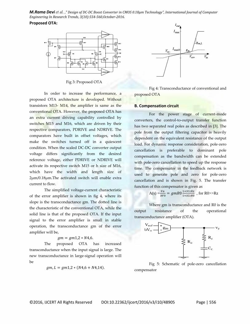
Settling Time and Ripple Voltage as shown in table 1.
M.Rama Devi et al. ," Design of DC-DC Boost Converter in CMOS 0.18µm Technology”, International Journal of Computer
Engineering In Research Trends, 3(10):554-560,October-2016.
©2016, IJCERT All Rights Reserved DOI:10.22362/ijcert/2016/v3/i10/48905 Page | 559
Parameter
Voltage
Mode
Control With
Conventional
OTA
Current
Mode
Control With
Conventional
OTA
Current
Mode
Control
With
Proposed
OTA
Settling
Time
8.5348ms
8.0916ms
7.284ms
Ripple
Voltage
17.32mV
17.32mV
13.33mV
Table: Results comparison
Fig 11: Implementation of Current Mode
Control Schematic using proposed OTA
To control this quiescent current, the soft-
start technique is used in this design. Figure 12
shows the regulated output voltage with controlled
quiescent current, simulated with proposed error
amplifier for fast transient response. As the output
voltage variation becomes large, the new error
amplifier supplies extra current for fast settling.
In order to evaluate the load regulation of
the controller, a load is changed from 100Ω to 1.5KΩ
at 1mSec. The regulated output voltage at various
load conditions in CMC mode converter is shown in
Figure 13.
Fig 12: Output voltage with controlled
quiescent current
Fig 13: CMC mode DC-DC boost converter
output with load regulation
IV. CONCLUSION
In order to reduce the power dissipation and
leakage current a switching type regulator with an
inductor as its storage element is used. By using
conventional OTA, the settling time is large for a DC-
DC boost converter operated CMC. To avoid this
problem a proposed OTA is used in the CMC to
reduce the settling time. A schematic level of the
proposed OTA based DC-DC boost converter in
CMC is implemented in 0.18µm CMOS technology
with a switching frequency of 500MHz. By using the
proposed OTA the design of Current mode CMOS
DC-DC boost converter reduces settling time from
8.53ms to 7.28ms and also it reduces the ripple
voltage from 17.32mv to 13.33mv. Hence, the
simulation results show that the designed converter
is 90% power efficient when the load current in the
order of 50mA.

M.Rama Devi et al. ," Design of DC-DC Boost Converter in CMOS 0.18µm Technology”, International Journal of Computer
Engineering In Research Trends, 3(10):554-560,October-2016.
©2016, IJCERT All Rights Reserved DOI:10.22362/ijcert/2016/v3/i10/48905 Page | 560
REFERENCES
[1] Ned Mohan, Tore M. Undeland, William P.
Robbins, “Power Electronics: Converters,
Applications, and Design”, 3rd Edition, Wiley.
[2] Robert W Erickson, Fundamentals of Power
Electronics, International Thomson Publishing
(1997)
[3] C. F. Lee and P. K. T. Mok, “A monolithic
current-mode CMOS DC-DC converter with on-
chip current-sensing technique,” IEEE J. Solid-
state Circuits, vol. 39, no. 1, pp. 3–14, Jan. 2004.
[4] Yushan Li, Kevin R. Vannorsdel, Art J. Zirger,
Mark Norris, and DraganMaksimovi´c, “Current
Mode Control for Boost Converters with
Constant Power Loads,” in IEEE Transactions on
Circuits and Systems-I: Regular Papers, vol. 59,
no. 1, pp. 198-206, January 2012.
[5] Weiwei Huang,Xiao Yang,Chaodong
Ling,”Novel current sensing circuit for boost
DC-DC converter”
[6] Kalpesh B. Pandya, Kehul A. shah “Performance
Evaluation of Different Types of CMOS
Operational Transconductance Amplifier”
International Journal of Science and Research
(IJSR), India Online ISSN: 2319-7064.
[7] HyunseokNam,InseokKim,YoungkookAhn,andJ
eongjinRoh,”A High efficiency Boost converter
for TFT-LCD bias supply”, THE 23rd
international Technical conference on
circuits/systems, computers and
communications (ITC-CSCC 2008).


![Vol. 2, Issue 9, September 2013 DESIGN OF DC-DC BOOST ... · DESIGN OF DC-DC BOOST CONVERTER WITH THERMOELECTRIC POWER SOURCE ... [2-4].In this research, DC-DC boost converter is](https://img.pdfslide.net/doc/110x75/5aec36db7f8b9ae5318ea3af/vol-2-issue-9-september-2013-design-of-dc-dc-boost-of-dc-dc-boost-converter.jpg)