Embed Size (px)
Citation preview
Proceedings of 10th Global Engineering, Science and Technology Conference 2-3 January, 2015, BIAM Foundation, Dhaka, Bangladesh, ISBN: 978-1-922069-69-6
1
High Voltage Gain DC-DC Boost Converter for PV Cells
Md. Al Muzahid1, Md. Fahmi Reza Ansari2, K. M. A. Salam3 and Hasan U. Zaman4
Regular small scale photovoltaic (PV) cells do not provide enough high voltage. As a result, a high voltage gain converter is essential. By using traditional boost converters, we cannot achieve the required high voltage gain, even with an extreme duty cycle. Therefore, a DC-DC boost converter is proposed in this paper for achieving high voltage gain by coupling inductors and the voltage lift technique. It is designed especially for high voltage conversion ratio applications such as providing power to an electric motor. By combining coupled inductors and the voltage lift technique, the energy stored in leakage inductor is recycled. As a result, a reduction of the switch turn-off voltage and implementation of soft switching turn-on operation are accomplished. In this paper, the operating principle and steady-state analysis of the continuous-conduction mode are discussed in detail. The clock frequency of 50 KHz and 24V DC from the photovoltaic cells can be converted to a 240V DC voltage output, which can be implemented using this converter. The simulation work was done using PSIM software.
Field of Research: Electrical and Electronic Engineering.
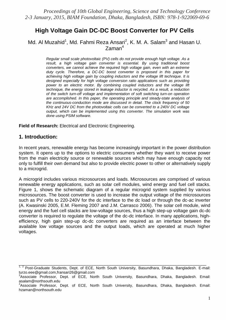
1. Introduction: In recent years, renewable energy has become increasingly important in the power distribution system. It opens up to the options to electric consumers whether they want to receive power from the main electricity source or renewable sources which may have enough capacity not only to fulfill their own demand but also to provide electric power to other or alternatively supply to a microgrid. A microgrid includes various microsources and loads. Microsources are comprised of various renewable energy applications, such as solar cell modules, wind energy and fuel cell stacks. Figure 1, shows the schematic diagram of a regular microgrid system supplied by various microsources. The boost converter is used to increase the output voltage of the microsources such as PV cells to 220-240V for the dc interface to the dc load or through the dc-ac inverter (A. Kwasinski 2005, E.M. Fleming 2007 and J.M. Carrasco 2006). The solar cell module, wind energy and the fuel cell stacks are low-voltage sources, thus a high step-up voltage gain dc-dc converter is required to regulate the voltage of the dc-dc interface. In many applications, high-efficiency, high gain step-up dc-dc converters are required as an interface between the available low voltage sources and the output loads, which are operated at much higher voltages. __________________________________________________________________________ 1, 2
Post-Graduate Students, Dept. of ECE, North South University, Basundhara, Dhaka, Bangladesh. E-mail: [email protected],[email protected] 3Associate Professor, Dept. of ECE, North South University, Basundhara, Dhaka, Bangladesh. Email:
[email protected] 4Associate Professor, Dept. of ECE, North South University, Basundhara, Dhaka, Bangladesh. Email:
Proceedings of 10th Global Engineering, Science and Technology Conference 2-3 January, 2015, BIAM Foundation, Dhaka, Bangladesh, ISBN: 978-1-922069-69-6
2
Figure 1. General power conversion system with a high voltage gain boost converter.
The traditional boost converters cannot provide such a high dc voltage gain, even for an extreme duty cycle. It also may cause reverse-recovery problem and increase the rating of all devices, which may eventually cause the conversion efficiency to decrease and the electromagnetic interference (EMI) can affect the whole system. (N. Mohan 1995) The coupled-inductor boost converter can be a substitute for the traditional boost converters to solve this issue. Because the turn’s ratio of the primary inductor (L1) to the secondary inductor (L2) of the coupled inductor can be efficient to reduce the duty ratio and the voltage stress of the switch. (Hyun-Lark Do 2011, Kuo-Ching Tseng 2013, Sanghyuk Lee 2013, Wuhua Li 2012, Yen-Mo Chen 2013 and Yi Zhao 2013) To reduce the voltage stress of the primary-side active switches and secondary-side rectifier diodes, a new voltage-multiplier circuit has been integrated. Based on the capacitor-divider concept, voltage-multiplier circuit is used to store energy in the output clamping capacitors and to share voltage stresses of both the active switches and rectifier diodes, which improves the conversion efficiency and reduces the reverse-recovery problem of the rectifier diodes. (Jung-Min Kwon 2009) In the proposed converter, the turn’s ratio of the coupled inductors can be designed to extend the voltage gain. A voltage-lift capacitor offers an extra voltage conversion ratio. The advantages of the proposed converter are as follows:
1. The converter is characterized by a low input current ripple and low conduction loss, making it suitable for high power applications.
2. The converter achieves the high step-up voltage gain that renewable energy systems require.
3. Leakage energy is recycled and sent to the output terminal, which improves large voltage spikes on the main switch.
4. The voltage stress in the main switch of the converter is substantially lower than the output voltage.
5. Low cost and high efficiency are achieved by the low rds. (on) and low voltage rating of the power switching device. Primary windings of the coupled inductors with Np turns are employed to decrease input current ripple, and secondary windings of the coupled inductors with Ns turns are connected in series to extend voltage gain. (Kuo-Ching Tseng 2013)
Proceedings of 10th Global Engineering, Science and Technology Conference 2-3 January, 2015, BIAM Foundation, Dhaka, Bangladesh, ISBN: 978-1-922069-69-6
3
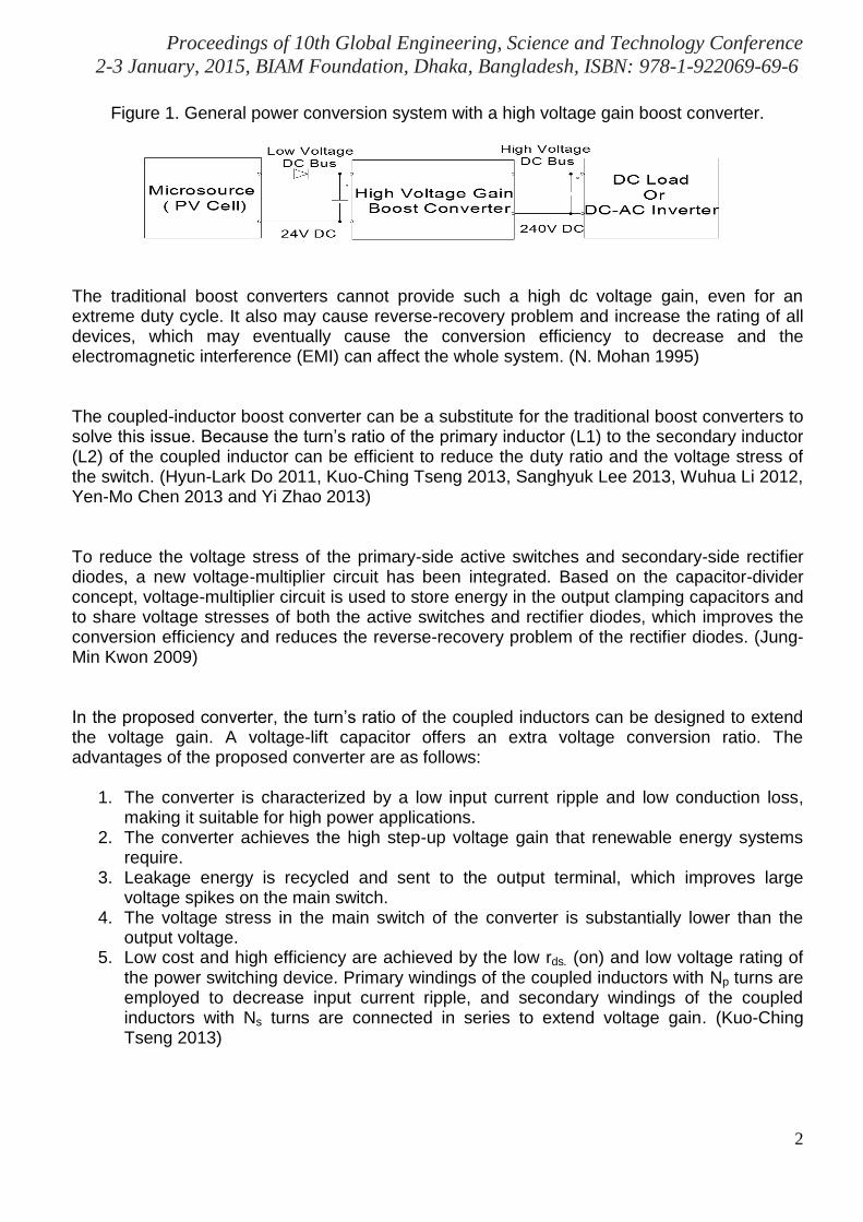
2. Projected boost converter and operating principle: Figure 2, shows the schematic diagram of the high voltage gain DC-DC boost converter for PV cell applications. The equivalent circuit of the coupled inductor includes the magnetizing inductor Lm, leakage inductors Lk1 and Lk2 and an ideal transformer. Other components of this converter are a dc input voltage Vin, one power switch, one coupled inductor, five diodes and three capacitors. The boost converter is designed to generate a stable voltage VC1 and to supply the energy for the load. Additionally, the diode D4 is turned on when switch S is in turned off period, the voltage across switch S is clamped at a low voltage level and the energy stored in the leakage inductance is recycled into C1. Since switch S has a low voltage rating and low conduction resistance rds (on), the proposed converter has high efficiency. Capacitors VC01 and VC02 provide the stable energy to output to ensure proper implementation of the voltage lifting technique. In addition, the turn’s ratio of the coupled inductor is adjusted to achieve a high step-up voltage gain. In this proposed converter, the duty ratio is designed to be 0.55 by adjusting the turn’s ratio of the coupled inductor. Thus the converter can be operated under Continuous Conduction Mode (CCM) and use low-rating switches and diodes to minimize the cost.
Figure 2. Circuit diagram of the proposed converter.
To simplify the circuit analysis, the following conditions are assumed:
1. Capacitors C1, C01 and C02 are large enough that VC1, VC01, and VC02 are constant during one switching period.
2. All semiconductor components are ideal. 3. Most of the energy is stored in the magnetizing inductance Lm, which is larger than the
leakage inductances Lk1 and Lk2. 4. Turns ratio of the coupled inductor is n=Ns/Np.
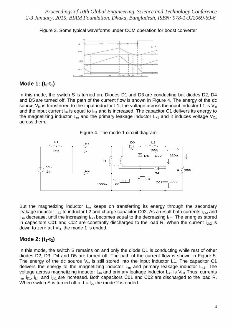
2.1 Operation of the proposed converter: The proposed converter operating in continuous conduction mode has been analyzed using the PSIM software. Figure 3, illustrates some typical waveforms under CCM operation in one switching period. The operating principle of CCM is divided into five modes during each switching period. The operating modes are described below:
Proceedings of 10th Global Engineering, Science and Technology Conference 2-3 January, 2015, BIAM Foundation, Dhaka, Bangladesh, ISBN: 978-1-922069-69-6
4
Figure 3. Some typical waveforms under CCM operation for boost converter
Mode 1: (t0-t1) In this mode, the switch S is turned on. Diodes D1 and D3 are conducting but diodes D2, D4 and D5 are turned off. The path of the current flow is shown in Figure 4. The energy of the dc source Vin is transferred to the input inductor L1, the voltage across the input inductor L1 is Vin and the input current iin is equal to iD1 and is increased. The capacitor C1 delivers its energy to the magnetizing inductor Lm and the primary leakage inductor Lk1 and it induces voltage VC1
across them.
Figure 4. The mode 1 circuit diagram
But the magnetizing inductor Lm keeps on transferring its energy through the secondary leakage inductor Lk2 to inductor L2 and charge capacitor C02. As a result both currents iLk2 and iLm decrease, until the increasing iLk1 becomes equal to the decreasing iLm. The energies stored in capacitors C01 and C02 are constantly discharged to the load R. When the current iLk2 is down to zero at t =t1, the mode 1 is ended.
Mode 2: (t1-t2) In this mode, the switch S remains on and only the diode D1 is conducting while rest of other diodes D2, D3, D4 and D5 are turned off. The path of the current flow is shown in Figure 5. The energy of the dc source Vin is still stored into the input inductor L1. The capacitor C1 delivers the energy to the magnetizing inductor Lm and primary leakage inductor Lk1. The voltage across magnetizing inductor Lm and primary leakage inductor Lk1 is VC1.Thus, currents iin, iD1, iLm and iLk1 are increased. Both capacitors C01 and C02 are discharged to the load R. When switch S is turned off at t = t2, the mode 2 is ended.
Proceedings of 10th Global Engineering, Science and Technology Conference 2-3 January, 2015, BIAM Foundation, Dhaka, Bangladesh, ISBN: 978-1-922069-69-6
5
Figure 5. The mode 2 circuit diagram
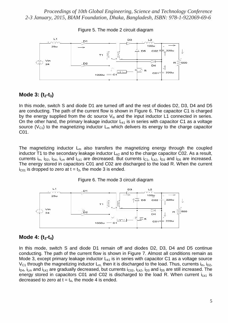
Mode 3: (t2-t3) In this mode, switch S and diode D1 are turned off and the rest of diodes D2, D3, D4 and D5
are conducting. The path of the current flow is shown in Figure 6. The capacitor C1 is charged by the energy supplied from the dc source Vin and the input inductor L1 connected in series. On the other hand, the primary leakage inductor Lk1 is in series with capacitor C1 as a voltage source (VC1) to the magnetizing inductor Lm which delivers its energy to the charge capacitor C01. The magnetizing inductor Lm also transfers the magnetizing energy through the coupled inductor T1 to the secondary leakage inductor Lk2 and to the charge capacitor C02. As a result, currents iin, iD2, iD4, iLm and iLk1 are decreased. But currents iC1, iLk2, iD3 and iD5 are increased. The energy stored in capacitors C01 and C02 are discharged to the load R. When the current iC01 is dropped to zero at t = t3, the mode 3 is ended.
Figure 6. The mode 3 circuit diagram
Mode 4: (t3-t4) In this mode, switch S and diode D1 remain off and diodes D2, D3, D4 and D5 continue conducting. The path of the current flow is shown in Figure 7. Almost all conditions remain as Mode 3, except primary leakage inductor Lk1 is in series with capacitor C1 as a voltage source VC1 through the magnetizing inductor Lm, then it is discharged to the load. Thus, currents iin, iD2, iD4, iLm and iLk1 are gradually decreased, but currents iC02, iLk2, iD3 and iD5 are still increased. The energy stored in capacitors C01 and C02 is discharged to the load R. When current iLk1 is decreased to zero at t = t4, the mode 4 is ended.
Proceedings of 10th Global Engineering, Science and Technology Conference 2-3 January, 2015, BIAM Foundation, Dhaka, Bangladesh, ISBN: 978-1-922069-69-6
6
Figure 7. The mode 4 circuit diagram
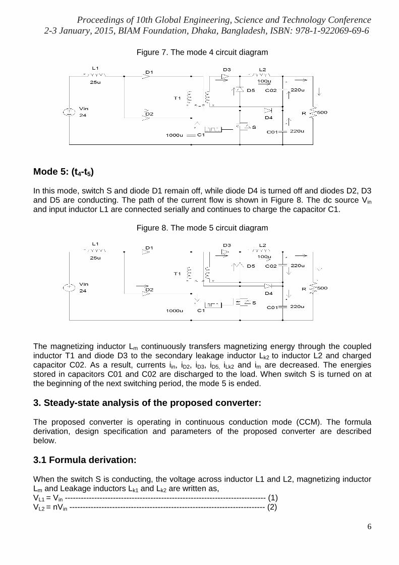
Mode 5: (t4-t5) In this mode, switch S and diode D1 remain off, while diode D4 is turned off and diodes D2, D3 and D5 are conducting. The path of the current flow is shown in Figure 8. The dc source Vin and input inductor L1 are connected serially and continues to charge the capacitor C1.
Figure 8. The mode 5 circuit diagram
The magnetizing inductor Lm continuously transfers magnetizing energy through the coupled inductor T1 and diode D3 to the secondary leakage inductor Lk2 to inductor L2 and charged capacitor C02. As a result, currents iin, iD2, iD3, iD5, iLk2 and im are decreased. The energies stored in capacitors C01 and C02 are discharged to the load. When switch S is turned on at the beginning of the next switching period, the mode 5 is ended.
3. Steady-state analysis of the proposed converter: The proposed converter is operating in continuous conduction mode (CCM). The formula derivation, design specification and parameters of the proposed converter are described below.
3.1 Formula derivation: When the switch S is conducting, the voltage across inductor L1 and L2, magnetizing inductor Lm and Leakage inductors Lk1 and Lk2 are written as, VL1 = Vin --------------------------------------------------------------------------- (1) VL2 = nVin ------------------------------------------------------------------------- (2)

Proceedings of 10th Global Engineering, Science and Technology Conference 2-3 January, 2015, BIAM Foundation, Dhaka, Bangladesh, ISBN: 978-1-922069-69-6
7
Where, n is the turn’s ratio,
--------------------------------------------------- (3)
Where, k is the coupling coefficient,
Applying KVL, VLk1 = VC1 – VLm = VC1 – kVC1 = VC1 (1-k) -------------------------------- (4) VLk2 = nVLm ----------------------------------------------------------------------- (5) When the switch S is turned off, the voltage across inductor L1, magnetizing inductor Lm and Leakage inductor Lk2 are written as, Applying KVL, VL1 = Vin – VC1 ------------------------------------------------------------------ (6) VLm = VC1 - VC01 – VLk1 -------------------------------------------------------- (7) VLk2 = nVLm + VL2 – VC02 ------------------------------------------------------ (8) By using Voltage-Second Balance Principal on Np and Ns of the coupled inductor, the following equations can be written, The voltage across the inductor L1 is,
∫
∫
------------------------------------------ (9)
The voltage across the magnetizing inductor Lm is,
∫
∫
---------------------------- (10)
From equation (9), VC1 is derived as,
----------------------------------------------------------------------- (11)
From equations (4), (10) and (11), VC01 is derived as,
----------------------------------------------------------------- (12)
From equations (2), (5) and (8), VC02 is derived as, VC02 = nVin --------------------------------------------------------------------- (13) The output voltage VR express as, VR = VC01 + VC02 -------------------------------------------------------------- (14) From equations (12), (13) and (14), VR is derived as,
--------------------------------------------------------- (15)
As a result, from equation (15), the voltage gain of the proposed boost converter can be represented as,
------------------------------------------------------ (16)
So, equation (16) indicates that, the proposed converter achieves a high voltage gain, if the value of duty cycle is increased or the turn ratio of the coupled inductor is increased. From equation (15), the output current iR is derived as,
------------------------------------- (17)
3.2 Design specification and parameters of the proposed converter:

Proceedings of 10th Global Engineering, Science and Technology Conference 2-3 January, 2015, BIAM Foundation, Dhaka, Bangladesh, ISBN: 978-1-922069-69-6
8
Based on above circuit specification, the circuit design specification and parameters can be considered as follows.
3.2.1 Duty cycle: Maximum duty cycle is given by,
D 1 ∗η
o --------------------------------------------------------------------- (18)
Where, Vin = Input voltage Vo = Output voltage
η = Efficiency of the converter. From the above equation it can be observed that the output voltage is always greater than the input voltage and with the increase in the value of duty cycle, the output voltage is also increased. Therefore, the maximum operating duty cycle is selected nearly 0.55.
3.2.2 Design of coupled inductor and other inductors: Coupled inductor includes the magnetizing inductor Lm, leakage inductors Lk1 and Lk2 and an ideal transformer. Therefore the turn’s ratio n and coupling coefficient k of the ideal transformer are defined as,
Ns
Np ----------------------------------------------------------------------------- (19)
------------------------------------------------------------------------ (20)
The boost converter is operated in the continuous current mode i.e. the inductor current never falls to zero. So the inductor value is given by,
1 o
Δ L ∗f∗ o
Δ L ∗f∗ 2 ---------------------------------------------- (21)
2
Δ L ∗f∗ 2 --------------------------------------------------------------- (22)
Δ = Ripple current of the inductor L1. Δ 2= Ripple current of the inductor which should be maintained between 20% to 40% of the output current and is given by,
Δ 2 . 2 to . 4 ∗ ∗ o
---------------------------------------------------------- (23)
= maximum output current. From the equations (19), (20), (21), (22) and (23) we calculate the values of L1 = 25µH and L2 = 100µH. here Lm and Lk values are chosen in such a way that the value of k is almost equal to 1.
3.2.3 Design of the capacitors:

Proceedings of 10th Global Engineering, Science and Technology Conference 2-3 January, 2015, BIAM Foundation, Dhaka, Bangladesh, ISBN: 978-1-922069-69-6
9
The minimum value of the capacitance is maintained in order to keep the output voltage when the load value exceeds. The capacitance value is given by the Filter Capacitor selection,
C or C 2 ∗
f∗Δ o ---------------------------------------------------------------- (24)
To find the value of capacitor C1 we use the following equation,
C1 Δ L ∗
f∗ ------------------------------------------------------------------- (25)
From the equations (24) and (25) we calculate the values of C01 and C02 = 220µF and C1 = 1000µF.
3.2.4 Selection of the switching device: Power MOSFET is chosen as switch because of its cost effectiveness, high speed, low on state resistance, improved gating and high speed power switching. Square pulse waves operating at a frequency of 50 KHz drive the Power MOSFET.
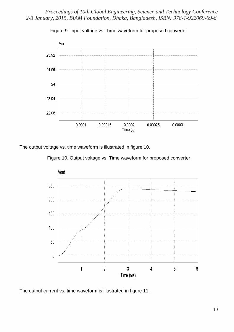
4. Simulation results: The proposed boost converter was simulated using the PSIM Simulator with the following specifications: Input DC voltage = 24V Output DC voltage = 240V Switching Frequency = 50 KHz Duty Cycle = 0.55 Inductors L1 and L2 = 25µH and 100µH Capacitors C1, C01 and C02 = 100µF, 220µF and 220µF Resistance R = 500Ω The photovoltaic cell supplies 24V DC to the circuit after being stabilized by a voltage stabilizer. Power MOSFET operating at 50 KHz frequency is used as the switching device. A resistive load is used for ideal operation of the circuit. The input voltage vs. time waveform is illustrated in figure 9.
Proceedings of 10th Global Engineering, Science and Technology Conference 2-3 January, 2015, BIAM Foundation, Dhaka, Bangladesh, ISBN: 978-1-922069-69-6
10
Figure 9. Input voltage vs. Time waveform for proposed converter
The output voltage vs. time waveform is illustrated in figure 10.
Figure 10. Output voltage vs. Time waveform for proposed converter
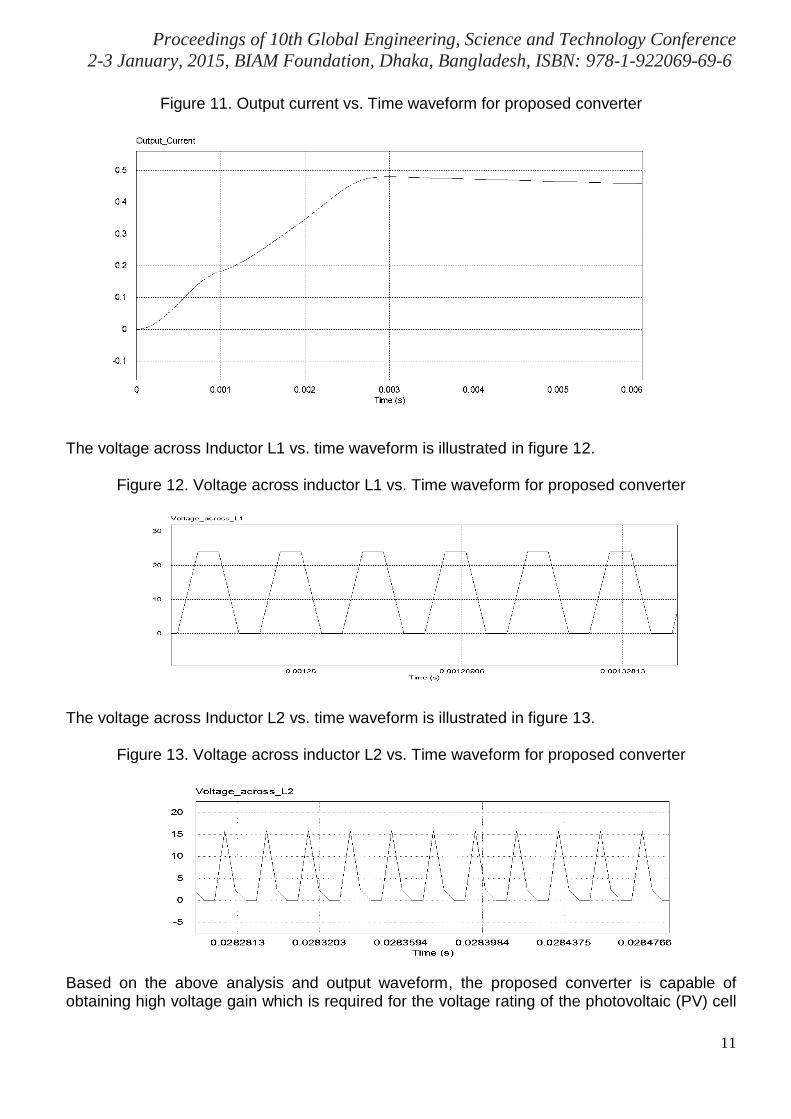
The output current vs. time waveform is illustrated in figure 11.
Proceedings of 10th Global Engineering, Science and Technology Conference 2-3 January, 2015, BIAM Foundation, Dhaka, Bangladesh, ISBN: 978-1-922069-69-6
11
Figure 11. Output current vs. Time waveform for proposed converter
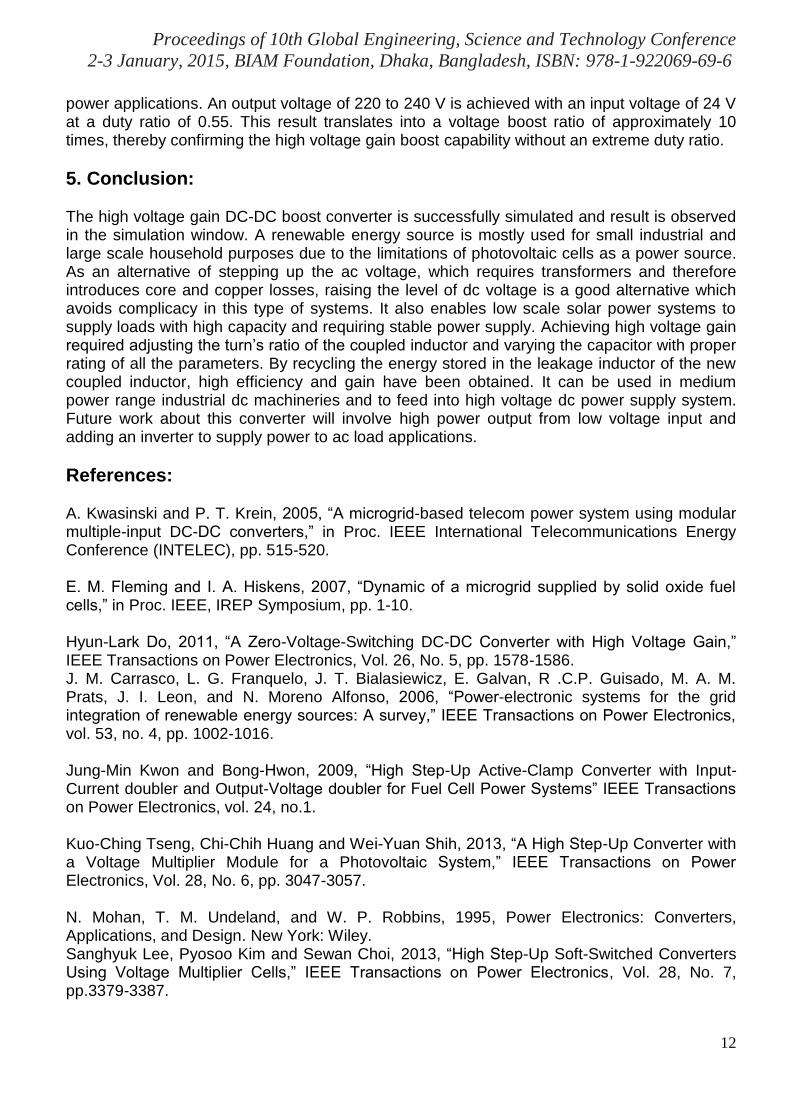
The voltage across Inductor L1 vs. time waveform is illustrated in figure 12.
Figure 12. Voltage across inductor L1 vs. Time waveform for proposed converter
The voltage across Inductor L2 vs. time waveform is illustrated in figure 13.
Figure 13. Voltage across inductor L2 vs. Time waveform for proposed converter
Based on the above analysis and output waveform, the proposed converter is capable of obtaining high voltage gain which is required for the voltage rating of the photovoltaic (PV) cell
Proceedings of 10th Global Engineering, Science and Technology Conference 2-3 January, 2015, BIAM Foundation, Dhaka, Bangladesh, ISBN: 978-1-922069-69-6
12
power applications. An output voltage of 220 to 240 V is achieved with an input voltage of 24 V at a duty ratio of 0.55. This result translates into a voltage boost ratio of approximately 10 times, thereby confirming the high voltage gain boost capability without an extreme duty ratio.
5. Conclusion: The high voltage gain DC-DC boost converter is successfully simulated and result is observed in the simulation window. A renewable energy source is mostly used for small industrial and large scale household purposes due to the limitations of photovoltaic cells as a power source. As an alternative of stepping up the ac voltage, which requires transformers and therefore introduces core and copper losses, raising the level of dc voltage is a good alternative which avoids complicacy in this type of systems. It also enables low scale solar power systems to supply loads with high capacity and requiring stable power supply. Achieving high voltage gain required adjusting the turn’s ratio of the coupled inductor and varying the capacitor with proper rating of all the parameters. By recycling the energy stored in the leakage inductor of the new coupled inductor, high efficiency and gain have been obtained. It can be used in medium power range industrial dc machineries and to feed into high voltage dc power supply system. Future work about this converter will involve high power output from low voltage input and adding an inverter to supply power to ac load applications.
References: A. Kwasinski and P. T. Krein, 2005, “A microgrid-based telecom power system using modular multiple-input DC-DC converters,” in Proc. IEEE International Telecommunications Energy Conference (INTELEC), pp. 515-520. E. M. Fleming and I. A. Hiskens, 2007, “Dynamic of a microgrid supplied by solid oxide fuel cells,” in Proc. IEEE, IREP Symposium, pp. 1-10. Hyun-Lark Do, 2011, “A Zero-Voltage-Switching DC-DC Converter with High Voltage Gain,” IEEE Transactions on Power Electronics, Vol. 26, No. 5, pp. 1578-1586. J. M. Carrasco, L. G. Franquelo, J. T. Bialasiewicz, E. Galvan, R .C.P. Guisado, M. A. M. Prats, J. I. Leon, and N. Moreno Alfonso, 2006, “Power-electronic systems for the grid integration of renewable energy sources: A survey,” IEEE Transactions on Power Electronics, vol. 53, no. 4, pp. 1002-1016. Jung-Min Kwon and Bong-Hwon, 2009, “High Step-Up Active-Clamp Converter with Input-Current doubler and Output-Voltage doubler for Fuel Cell Power Systems” IEEE Transactions on Power Electronics, vol. 24, no.1. Kuo-Ching Tseng, Chi-Chih Huang and Wei-Yuan Shih, 2013, “A High Step-Up Converter with a Voltage Multiplier Module for a Photovoltaic System,” IEEE Transactions on Power Electronics, Vol. 28, No. 6, pp. 3047-3057. N. Mohan, T. M. Undeland, and W. P. Robbins, 1995, Power Electronics: Converters, Applications, and Design. New York: Wiley. Sanghyuk Lee, Pyosoo Kim and Sewan Choi, 2013, “High Step-Up Soft-Switched Converters Using Voltage Multiplier Cells,” IEEE Transactions on Power Electronics, Vol. 28, No. 7, pp.3379-3387.

Proceedings of 10th Global Engineering, Science and Technology Conference 2-3 January, 2015, BIAM Foundation, Dhaka, Bangladesh, ISBN: 978-1-922069-69-6
13
Wuhua Li, Weichen Li, Xiangning He, David Xu and Bin Wu, 2012,“General Derivation Law of Non isolated High-Step-Up Interleaved Converters With Built-In Transformer,” IEEE Transactions on Industrial Electronics, Vol. 59, No. 3, pp. 1650-1661. Yen-Mo Chen, Alex Q. Huang and Xunwei Yu, 2013, “A High Step-Up Three-Port DC-DC Converter for Stand-Alone PV/Battery Power Systems,” IEEE Transactions on Power Electronics, Vol. 28, No. 11, pp. 5049-5062. Yi Zhao, Xin Xiang, Wuhua Li, Xiangning He and Changliang Xia, 2013, “Advanced Symmetrical Voltage Quadrupler Rectifiers for High Step-Up and High Output-Voltage Converters,” IEEE Transactions on Power Electronics, Vol. 28, No. 4, pp.1622-1631.