Embed Size (px)
Citation preview

MSP430F2618-EPMIXED SIGNAL MICROCONTROLLER
SLAS632 -- DECEMBER 2008
1POST OFFICE BOX 655303 DALLAS, TEXAS 75265
FEATURES
D Low Supply Voltage Range, 1.8 V to 3.6 VD Ultra-Low Power Consumption:
-- Active Mode: 365 A at 1 MHz, 2.2 V-- Standby Mode (VLO): 0.5 A-- Off Mode (RAM Retention): 0.1 A
D Wake-Up From Standby Mode in LessThan 1 s
D 16-Bit RISC Architecture,62.5-ns Instruction Cycle Time
D Three-Channel Internal DMAD 12-Bit Analog-to-Digital (A/D) Converter
With Internal Reference, Sample-and-Hold,and Autoscan Feature
D Dual 12-Bit Digital-to-Analog (D/A)Converters With Synchronization
D 16-Bit Timer_A With ThreeCapture/Compare Registers
D 16-Bit Timer_B With SevenCapture/Compare-With-Shadow Registers
D On-Chip ComparatorD Four Universal Serial Communication
Interfaces (USCIs)-- USCI_A0 and USCI_A1
-- Enhanced UART SupportingAuto-Baudrate Detection
-- IrDA Encoder and Decoder-- Synchronous SPI
-- USCI_B0 and USCI_B1-- I2Ct-- Synchronous SPI
D Supply Voltage Supervisor/Monitor WithProgrammable Level Detection
D Brownout DetectorD Bootstrap LoaderD Serial Onboard Programming,
No External Programming Voltage NeededProgrammable Code Protection by SecurityFuse
D 116KB+256B Flash Memory, 8KB RAMD Available in 113-Pin Ball Grid Array (BGA)D For Complete Module Descriptions, See the
MSP430x2xx Family User’s Guide,Literature Number SLAU144
SUPPORTS DEFENSE, AEROSPACE, ANDMEDICAL APPLICATIONSD Controlled BaselineD One Assembly/Test SiteD One Fabrication SiteD Extended Product Life CycleD Extended Product--Change NotificationD Product TraceabilityD SnPb Solder Ball Alloy for Increased
Reliability
description
The Texas Instruments MSP430 family of ultralow-power microcontrollers consists of several devices featuringdifferent sets of peripherals targeted for various applications. The architecture, combined with five low-powermodes is optimized to achieve extended battery life in portable measurement applications. The device featuresa powerful 16-bit RISC CPU, 16-bit registers, and constant generators that contribute to maximum codeefficiency. The calibrated digitally controlled oscillator (DCO) allows wake-up from low-power modes to activemode in less than 1 s.
This integrated circuit can be damaged by ESD. Texas Instruments recommends that all integrated circuits be handled withappropriate precautions. Failure toobserve properhandling and installation procedures can causedamage. ESDdamagecan rangefrom subtle performance degradation to complete device failure. Precision integrated circuits may be more susceptible to damagebecause very small parametric changes could cause the device not tomeet its published specifications. These devices have limitedbuilt-in ESD protection.
Copyright 2008, Texas Instruments Incorporated
Please be aware that an important notice concerning availability, standard warranty, and use in critical applications ofTexas Instruments semiconductor products and disclaimers thereto appears at the end of this data sheet.
I2C is a registered trademark of Philips Incorporated.
PRODUCTION DATA information is current as of publication date.Products conform to specifications per the terms of Texas Instrumentsstandard warranty. Production processing does not necessarily includetesting of all parameters.

MSP430F2618-EPMIXED SIGNAL MICROCONTROLLER
SLAS632 -- DECEMBER 2008
2 POST OFFICE BOX 655303 DALLAS, TEXAS 75265
description (continued)
The MSP430F2618 is a microcontroller configuration with two built-in 16-bit timers, a fast 12-bit A/D converter,a comparator, dual 12-bit D/A converters, four universal serial communication interface (USCI) modules, DMA,and up to 64 I/O pins. Typical applications include sensor systems, industrial control applications, hand-heldmeters, etc.
AVAILABLE OPTIONS
TPACKAGED DEVICES
TA PLASTIC 113-PIN BGA (GQW)
--40C to 105C MSP430F2618TGQW
DEVELOPMENT TOOL SUPPORT
All MSP430 microcontrollers include an Embedded Emulation Module (EEM) allowing advanced debuggingand programming through easy-to-use development tools. Recommended hardware options include:
D Debugging and Programming Interface
-- MSP-FET430UIF (USB)
-- MSP-FET430PIF (Parallel Port)
D Debugging and Programming Interface with Target Board
-- MSP-FET430U64
-- MSP-FET430U80
D Standalone Target Board
-- MSP-TS430PM64
D Production Programmer
-- MSP-GANG430

MSP430F2618-EPMIXED SIGNAL MICROCONTROLLER
SLAS632 -- DECEMBER 2008
3POST OFFICE BOX 655303 DALLAS, TEXAS 75265
pin designation
Note: For terminal assignments, see the MSP430F261x Terminal Functions table.
A1
B1
C1
D1
E1
F1
G1
H1
J1
K1
L1
M1
A2
B2
C2
D2
E2
F2
G2
H2
J2
K2
L2
M2
A3 A4 A5 A6 A7 A8 A9 A10
E5 E6 E7 E8
A11
B11
C11
D11
E11
F11
G11
H11
J11
K11
L11
M11
A12
B12
C12
D12
E12
F12
G12
H12
J12
K12
L12
M12M3 M4 M5 M6 M7 M8 M9 M10
L3 L4 L5 L6 L7 L8 L9 L10
B3 B4 B5 B6 B7 B8 B9 B10
H5 H6 H7 H8
D4 D5 D6 D7 D8 D9
E4
F4
G4
H4
F5
G5
F8
G8
E9
F9
G9
H9
C3
J4 J5 J6 J7 J8 J9

MSP430F2618-EPMIXED SIGNAL MICROCONTROLLER
SLAS632 -- DECEMBER 2008
4 POST OFFICE BOX 655303 DALLAS, TEXAS 75265
functional block diagram
OscillatorsBasic Clock
System+
Brownout Protection
SVS,SVM
RST/NMI
DVCC1/2 DVSS1/2
MCLK
WatchdogWDT+
15-Bit
Timer_A3
3 CC Registers
16MHzCPU1MB
incl. 16 Registers
Emulation
JTAGInterface
Ports P1/P2
2x8 I/O Interrupt capability
Comp_A+
8 Channels
Hardware Multiplier
MPY, MPYS, MAC, MACS
Timer_B7
7 CC Registers, Shadow
Reg
ADC1212-Bit
8 Channels
PortsP3/P4P5/P6
4x8 I/O
AVCC AVSS P1.x/P2.x
2x8
P3.x/P4.xP5.x/P6.x
4x8
SMCLK
ACLK
MDB
MAB
DAC1212-Bit
2 Channels Voltage
Out
PortsP7/P8
2x8/1x16 I/O
P7.x/P8.x2x8/1x16
DMA Controller
3 Channels
XIN/XT2IN
22
XOUT/XT2OUT
RAM
4kB8kB8kB4kB4kB
Flash
120kB116kB92kB92kB56kB
USCI A1UART/
LIN,IrDA, SPI
USCI B1SPI, I2C
USCI A0UART/
LIN,IrDA, SPI
USCI B0SPI, I2C

MSP430F2618-EPMIXED SIGNAL MICROCONTROLLER
SLAS632 -- DECEMBER 2008
5POST OFFICE BOX 655303 DALLAS, TEXAS 75265
Terminal Functions
TERMINALI/O DESCRIPTION
NAME NOI/O DESCRIPTION
NAME NO./
AVCC A2Analog supply voltage, positive terminal. Supplies only the analog portion of ADC12 andDAC12.
AVSS B2, B3Analog supply voltage, negative terminal. Supplies only the analog portion of ADC12 andDAC12.
DVCC1 A1 Digital supply voltage, positive terminal. Supplies all digital parts.
DVSS1 A3 Digital supply voltage, negative terminal. Supplies all digital parts.
DVCC2 F12 Digital supply voltage, positive terminal. Supplies all digital parts.
DVSS2 E12 Digital supply voltage, negative terminal. Supplies all digital parts.
P1.0/TACLK/CAOUT G2 I/O General-purpose digital I/O pin/Timer_A, clock signal TACLK input/Comparator_A output
P1.1/TA0 H1 I/OGeneral-purposedigital I/Opin/Timer_A, capture: CCI0A input, compare:Out0output/BSLtransmit
P1.2/TA1 H2 I/O General-purpose digital I/O pin/Timer_A, capture: CCI1A input, compare: Out1 output
P1.3/TA2 J1 I/O General-purpose digital I/O pin/Timer_A, capture: CCI2A input, compare: Out2 output
P1.4/SMCLK J2 I/O General-purpose digital I/O pin/SMCLK signal output
P1.5/TA0 K1 I/O General-purpose digital I/O pin/Timer_A, compare: Out0 output
P1.6/TA1 K2 I/O General-purpose digital I/O pin/Timer_A, compare: Out1 output
P1.7/TA2 L1 I/O General-purpose digital I/O pin/Timer_A, compare: Out2 output
P2.0/ACLK/CA2 M1 I/O General-purpose digital I/O pin/ACLK output/Comparator_A input
P2.1/TAINCLK/CA3 M2 I/O General-purpose digital I/O pin/Timer_A, clock signal at INCLK
P2.2/CAOUT/TA0/CA4 M3 I/O
General-purpose digital I/O pin/Timer_A, capture: CCI0B input/Comparator_A output/BSLreceive/Comparator_A input
P2.3/CA0/TA1 L3 I/O General-purpose digital I/O pin/Timer_A, compare: Out1 output/Comparator_A input
P2.4/CA1/TA2 L4 I/O General-purpose digital I/O pin/Timer_A, compare: Out2 output/Comparator_A input
P2.5/Rosc/CA5 M4 I/OGeneral-purpose digital I/O pin/input for external resistor defining the DCO nominalfrequency/Comparator_A input
P2.6/ADC12CLK/DMAE0/CA6 J4 I/O
General-purpose digital I/O pin/conversion clock – 12-bit ADC/DMA channel 0 externaltrigger/Comparator_A input
P2.7/TA0/CA7 L5 I/O General-purpose digital I/O pin/Timer_A, compare: Out0 output/Comparator_A input
P3.0/UCB0STE/UCA0CLK M5 I/O General-purpose digital I/O pin/USCI B0 slave transmit enable/USCI A0 clock input/output
P3.1/UCB0SIMO/UCB0SDA L6 I/O
General-purpose digital I/O pin/USCI B0 slave in/master out in SPI mode, SDA I2C data inI2C mode
P3.2/UCB0SOMI/UCB0SCL M6 I/O
General-purpose digital I/O pin/USCI B0 slave out/master in in SPI mode, SCL I2C clockin I2C mode
P3.3/UCB0CLK/UCA0STE L7 I/O General-purpose digital I/O/USCI B0 clock input/output, USCI A0 slave transmit enable
P3.4/UCA0TXD/UCA0SIMO M7 I/O
General-purpose digital I/O pin/USCIA transmit data output in UART mode, slave datain/master out in SPI mode
P3.5/UCA0RXD/UCA0SOMI L8 I/O
General-purpose digital I/O pin/USCI A0 receive data input in UART mode, slave dataout/master in in SPI mode
MSP430F2618-EPMIXED SIGNAL MICROCONTROLLER
SLAS632 -- DECEMBER 2008
6 POST OFFICE BOX 655303 DALLAS, TEXAS 75265
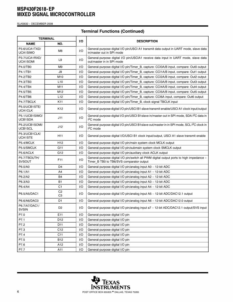
Terminal Functions (Continued)
TERMINALI/O DESCRIPTION
NAME NOI/O DESCRIPTION
NAME NO./
P3.6/UCA1TXD/UCA1SIMO M8 I/O
General-purpose digital I/O pin/USCI A1 transmit data output in UART mode, slave datain/master out in SPI mode
P3.7/UCA1RXD/UCA1SOMI L9 I/O
General-purpose digital I/O pin/USCIA1 receive data input in UART mode, slave dataout/master in in SPI mode
P4.0/TB0 M9 I/O General-purpose digital I/O pin/Timer_B, capture: CCI0A/B input, compare: Out0 output
P4.1/TB1 J9 I/O General-purpose digital I/O pin/Timer_B, capture: CCI1A/B input, compare: Out1 output
P4.2/TB2 M10 I/O General-purpose digital I/O pin/Timer_B, capture: CCI2A/B input, compare: Out2 output
P4.3/TB3 L10 I/O General-purpose digital I/O pin/Timer_B, capture: CCI3A/B input, compare: Out3 output
P4.4/TB4 M11 I/O General-purpose digital I/O pin/Timer_B, capture: CCI4A/B input, compare: Out4 output
P4.5/TB5 M12 I/O General-purpose digital I/O pin/Timer_B, capture: CCI5A/B input, compare: Out5 output
P4.6/TB6 L12 I/O General-purpose digital I/O pin/Timer_B, capture: CCI6A input, compare: Out6 output
P4.7/TBCLK K11 I/O General-purpose digital I/O pin/Timer_B, clock signal TBCLK input
P5.0/UCB1STE/UCA1CLK K12 I/O General-purpose digital I/O pin/USCI B1 slave transmit enable/USCI A1 clock input/output
P5.1/UCB1SIMO/UCB1SDA J11 I/O
General-purpose digital I/O pin/USCI B1slave in/master out in SPI mode, SDA I2C data inI2C mode
P5.2/UCB1SOMI/UCB1SCL J12 I/O
General-purpose digital I/O pin/USCI B1slave out/master in in SPI mode, SCL I2C clock inI2C mode
P5.3/UCB1CLK/UCA1STE H11 I/O General-purpose digital I/O/USCI B1 clock input/output, USCI A1 slave transmit enable
P5.4/MCLK H12 I/O General-purpose digital I/O pin/main system clock MCLK output
P5.5/SMCLK G11 I/O General-purpose digital I/O pin/submain system clock SMCLK output
P5.6/ACLK G12 I/O General-purpose digital I/O pin/auxiliary clock ACLK output
P5.7/TBOUTH/SVSOUT F11 I/O
General-purpose digital I/O pin/switch all PWM digital output ports to high impedance --Timer_B TB0 to TB6/SVS comparator output
P6.0/A0 D4 I/O General-purpose digital I/O pin/analog input A0 – 12-bit ADC
P6.1/A1 A4 I/O General-purpose digital I/O pin/analog input A1 – 12-bit ADC
P6.2/A2 B4 I/O General-purpose digital I/O pin/analog input A2 – 12-bit ADC
P6.3/A3 B1 I/O General-purpose digital I/O pin/analog input A3 – 12-bit ADC
P6.4/A4 C1 I/O General-purpose digital I/O pin/analog input A4 – 12-bit ADC
P6.5/A5/DAC1C2C3 I/O General-purpose digital I/O pin/analog input A5 – 12-bit ADC/DAC12.1 output
P6.6/A6/DAC0 D1 I/O General-purpose digital I/O pin/analog input A6 – 12-bit ADC/DAC12.0 output
P6.7/A7/DAC1/SVSIN D2 I/O General-purpose digital I/O pin/analog input a7 – 12-bit ADC/DAC12.1 output/SVS input
P7.0 E11 I/O General-purpose digital I/O pin
P7.1 D12 I/O General-purpose digital I/O pin
P7.2 D11 I/O General-purpose digital I/O pin
P7.3 C12 I/O General-purpose digital I/O pin
P7.4 C11 I/O General-purpose digital I/O pin
P7.5 B12 I/O General-purpose digital I/O pin
P7.6 A12 I/O General-purpose digital I/O pin
P7.7 A11 I/O General-purpose digital I/O pin

MSP430F2618-EPMIXED SIGNAL MICROCONTROLLER
SLAS632 -- DECEMBER 2008
7POST OFFICE BOX 655303 DALLAS, TEXAS 75265
Terminal Functions (Continued)
TERMINALI/O DESCRIPTION
NAME NOI/O DESCRIPTION
NAME NO./
P8.0 B10 I/O General-purpose digital I/O pin
P8.1 A10 I/O General-purpose digital I/O pin
P8.2 D9 I/O General-purpose digital I/O pin
P8.3 A9 I/O General-purpose digital I/O pin
P8.4 B9 I/O General-purpose digital I/O pin
P8.5 B8 I/O General-purpose digital I/O pin
P8.6/XT2OUT A8 O General-purpose digital I/O pin/Output terminal of crystal oscillator XT2
P8.7/XT2IN A7 IGeneral-purpose digital I/O pin/Input port for crystal oscillator XT2. Only standardcrystals can be connected.
XT2OUT O Output terminal of crystal oscillator XT2
XT2IN I Input port for crystal oscillator XT2
RST/NMI B5 IReset input, nonmaskable interrupt input port, or bootstrap loader start (in flashdevices).
TCK A5 ITest clock (JTAG). TCK is theclock inputport fordeviceprogramming test andbootstraploader start.
TDI/TCLK A6 I Test data input or test clock input. Thedevice protection fuse is connected toTDI/TCLK.
TDO/TDI B7 I/O Test data output port. TDO/TDI data output or programming data input terminal.
TMS B6 I Test mode select. TMS is used as an input port for device programming and test.
VeREF+/DAC0 F2 I Input for an external reference voltage/DAC12.0 output
VREF+ E2 O Output of positive terminal of the reference voltage in the ADC12
VREF--/VeREF-- G1 INegative terminal for the reference voltage for both sources, the internal referencevoltage, or an external applied reference voltage
XIN E1 I Input port for crystal oscillator XT1. Standard or watch crystals can be connected.
XOUT F1 O Output port for crystal oscillator XT1. Standard or watch crystals can be connected.
Reserved
L2, E4F4, G4H4, D5E5, F5G5, H5J5, D6E6, H6J6, D7E7, H7J7, D8E8, F8G8, H8J8, E9F9, G9H9, B11L11
NA Reserved pins. Connection to D/AVSS recommended.

General-Purpose Register
Program Counter
Stack Pointer
Status Register
Constant Generator
General-Purpose Register
General-Purpose Register
General-Purpose Register
PC/R0
SP/R1
SR/CG1/R2
CG2/R3
R4
R5
R12
R13
General-Purpose Register
General-Purpose Register
R6
R7
General-Purpose Register
General-Purpose Register
R8
R9
General-Purpose Register
General-Purpose Register
R10
R11
General-Purpose Register
General-Purpose Register
R14
R15
MSP430F2618-EPMIXED SIGNAL MICROCONTROLLER
SLAS632 -- DECEMBER 2008
8 POST OFFICE BOX 655303 DALLAS, TEXAS 75265
short-form description
CPU
The MSP430 CPU has a 16-bit RISC architecturethat is highly transparent to the application. Alloperations, other than program-flow instructions,are performed as register operations inconjunction with seven addressing modes forsource operand and four addressing modes fordestination operand.
The CPU is integrated with 16 registers thatprovide reduced instruction execution time. Theregister-to-register operation execution time isone cycle of the CPU clock.
Four of the registers, R0 to R3, are dedicated asprogram counter, stack pointer, status register,and constant generator, respectively. Theremaining registers are general-purposeregisters.
Peripherals are connected to the CPU using data,address, and control buses, and can be handledwith all instructions.
instruction set
The instruction set consists of 51 instructions withthree formats and seven address modes. Eachinstruction can operate on word and byte data.Table 1 shows examples of the three types ofinstruction formats; the address modes are listedin Table 2.
Table 1. Instruction Word Formats
Dual operands, source-destination e.g., ADD R4,R5 R4 + R5 ------> R5
Single operands, destination only e.g., CALL R8 PC ---->(TOS), R8----> PC
Relative jump, un/conditional e.g., JNE Jump-on-equal bit = 0
Table 2. Address Mode Descriptions
ADDRESS MODE S D SYNTAX EXAMPLE OPERATION
Register D D MOV Rs,Rd MOV R10,R11 R10 ----> R11
Indexed D D MOV X(Rn),Y(Rm) MOV 2(R5),6(R6) M(2+R5)----> M(6+R6)
Symbolic (PC relative) D D MOV EDE,TONI M(EDE) ----> M(TONI)
Absolute D D MOV &MEM,&TCDAT M(MEM) ----> M(TCDAT)
Indirect D MOV @Rn,Y(Rm) MOV @R10,Tab(R6) M(R10) ----> M(Tab+R6)
Indirectautoincrement D MOV @Rn+,Rm MOV @R10+,R11
M(R10) ----> R11R10 + 2----> R10
Immediate D MOV #X,TONI MOV #45,TONI #45 ----> M(TONI)
NOTE: S = source D = destination

MSP430F2618-EPMIXED SIGNAL MICROCONTROLLER
SLAS632 -- DECEMBER 2008
9POST OFFICE BOX 655303 DALLAS, TEXAS 75265
operating modes
The MSP430 has one active mode and five software-selectable low-power modes of operation. An interruptevent can wake up the device from any of the five low-power modes, service the request, and restore back tothe low-power mode on return from the interrupt program.
The following six operating modes can be configured by software:
D Active mode (AM)
-- All clocks are active.
D Low-power mode 0 (LPM0)
-- CPU is disabled.
-- ACLK and SMCLK remain active. MCLK is disabled.
D Low-power mode 1 (LPM1)
-- CPU is disabled.
-- ACLK and SMCLK remain active. MCLK is disabled.
-- DCO’s dc generator is disabled if DCO not used in active mode.
D Low-power mode 2 (LPM2)
-- CPU is disabled.
-- MCLK and SMCLK are disabled.
-- DCO’s dc generator remains enabled.
-- ACLK remains active.
D Low-power mode 3 (LPM3)
-- CPU is disabled.
-- MCLK and SMCLK are disabled.
-- DCO’s dc generator is disabled.
-- ACLK remains active.
D Low-power mode 4 (LPM4)
-- CPU is disabled.
-- ACLK is disabled.
-- MCLK and SMCLK are disabled.
-- DCO’s dc generator is disabled.
-- Crystal oscillator is stopped.
MSP430F2618-EPMIXED SIGNAL MICROCONTROLLER
SLAS632 -- DECEMBER 2008
10 POST OFFICE BOX 655303 DALLAS, TEXAS 75265
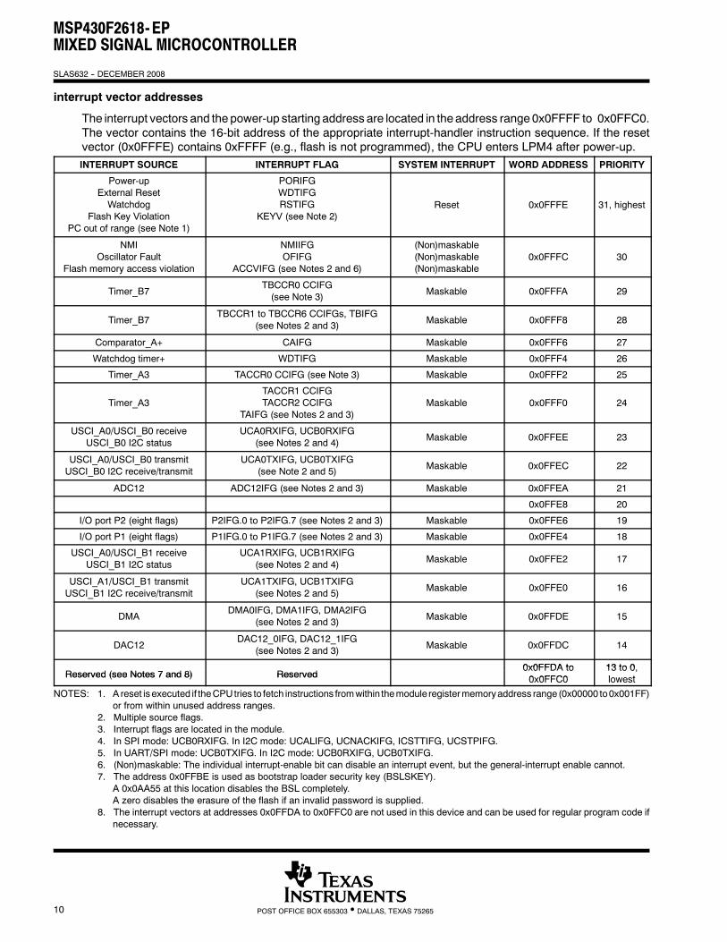
interrupt vector addresses
The interrupt vectors and the power-up starting address are located in the address range 0x0FFFF to 0x0FFC0.The vector contains the 16-bit address of the appropriate interrupt-handler instruction sequence. If the resetvector (0x0FFFE) contains 0xFFFF (e.g., flash is not programmed), the CPU enters LPM4 after power-up.INTERRUPT SOURCE INTERRUPT FLAG SYSTEM INTERRUPT WORD ADDRESS PRIORITY
Power-upExternal ResetWatchdog
Flash Key ViolationPC out of range (see Note 1)
PORIFGWDTIFGRSTIFG
KEYV (see Note 2)Reset 0x0FFFE 31, highest
NMIOscillator Fault
Flash memory access violation
NMIIFGOFIFG
ACCVIFG (see Notes 2 and 6)
(Non)maskable(Non)maskable(Non)maskable
0x0FFFC 30
Timer_B7TBCCR0 CCIFG(see Note 3) Maskable 0x0FFFA 29
Timer_B7TBCCR1 to TBCCR6 CCIFGs, TBIFG
(see Notes 2 and 3) Maskable 0x0FFF8 28
Comparator_A+ CAIFG Maskable 0x0FFF6 27
Watchdog timer+ WDTIFG Maskable 0x0FFF4 26
Timer_A3 TACCR0 CCIFG (see Note 3) Maskable 0x0FFF2 25
Timer_A3TACCR1 CCIFGTACCR2 CCIFG
TAIFG (see Notes 2 and 3)Maskable 0x0FFF0 24
USCI_A0/USCI_B0 receiveUSCI_B0 I2C status
UCA0RXIFG, UCB0RXIFG(see Notes 2 and 4) Maskable 0x0FFEE 23
USCI_A0/USCI_B0 transmitUSCI_B0 I2C receive/transmit
UCA0TXIFG, UCB0TXIFG(see Note 2 and 5) Maskable 0x0FFEC 22
ADC12 ADC12IFG (see Notes 2 and 3) Maskable 0x0FFEA 21
0x0FFE8 20
I/O port P2 (eight flags) P2IFG.0 to P2IFG.7 (see Notes 2 and 3) Maskable 0x0FFE6 19
I/O port P1 (eight flags) P1IFG.0 to P1IFG.7 (see Notes 2 and 3) Maskable 0x0FFE4 18
USCI_A0/USCI_B1 receiveUSCI_B1 I2C status
UCA1RXIFG, UCB1RXIFG(see Notes 2 and 4) Maskable 0x0FFE2 17
USCI_A1/USCI_B1 transmitUSCI_B1 I2C receive/transmit
UCA1TXIFG, UCB1TXIFG(see Notes 2 and 5) Maskable 0x0FFE0 16
DMADMA0IFG, DMA1IFG, DMA2IFG
(see Notes 2 and 3) Maskable 0x0FFDE 15
DAC12DAC12_0IFG, DAC12_1IFG
(see Notes 2 and 3) Maskable 0x0FFDC 14
0x0FFDA to 13 to 0Reserved (see Notes 7 and 8) Reserved
0x0FFDA to0 0FFC0
13 to 0,l tReserved (see Notes 7 and 8) Reserved 0x0FFC0 lowest
NOTES: 1. A reset isexecuted if theCPUtries to fetch instructions fromwithin themodule registermemoryaddress range(0x00000 to0x001FF)or from within unused address ranges.
2. Multiple source flags.3. Interrupt flags are located in the module.4. In SPI mode: UCB0RXIFG. In I2C mode: UCALIFG, UCNACKIFG, ICSTTIFG, UCSTPIFG.5. In UART/SPI mode: UCB0TXIFG. In I2C mode: UCB0RXIFG, UCB0TXIFG.6. (Non)maskable: The individual interrupt-enable bit can disable an interrupt event, but the general-interrupt enable cannot.7. The address 0x0FFBE is used as bootstrap loader security key (BSLSKEY).
A 0x0AA55 at this location disables the BSL completely.A zero disables the erasure of the flash if an invalid password is supplied.
8. The interrupt vectors at addresses 0x0FFDA to 0x0FFC0 are not used in this device and can be used for regular program code ifnecessary.

MSP430F2618-EPMIXED SIGNAL MICROCONTROLLER
SLAS632 -- DECEMBER 2008
11POST OFFICE BOX 655303 DALLAS, TEXAS 75265
special function registers
Most interrupt enable bits are collected in the lowest address space. Special-function register bits not allocatedto a functional purpose are not physically present in the device. This arrangement provides simple softwareaccess.
interrupt enable 1 and 2
Address 7 6 5 4 3 2 1 0
00h ACCVIE NMIIE OFIE WDTIE
rw--0 rw--0 rw--0 rw--0
Interrupt Enable Register 1
WDTIE Watchdog timer interrupt enable. Inactive if watchdog mode is selected.Active if watchdog timer is configured as general-purpose timer.
OFIE Oscillator fault interrupt enable
NMIIE Nonmaskable interrupt enable
ACCVIE Flash memory access violation interrupt enable
Address 7 6 5 4 3 2 1 0
01h UCB0TXIE UCB0RXIE UCA0TXIE UCA0RXIE
rw--0 rw--0 rw--0 rw--0
Interrupt Enable Register 2
UCA0RXIE USCI_A0 receive interrupt enable
UCA0TXIE USCI_A0 transmit interrupt enable
UCB0RXIE USCI_B0 receive interrupt enable
UCB0TXIE USCI_B0 transmit interrupt enable

MSP430F2618-EPMIXED SIGNAL MICROCONTROLLER
SLAS632 -- DECEMBER 2008
12 POST OFFICE BOX 655303 DALLAS, TEXAS 75265
interrupt flag register 1 and 2
Address 7 6 5 4 3 2 1 0
02h NMIIFG RSTIFG PORIFG OFIFG WDTIFG
rw--0 rw--(0) rw--(1) rw--1 rw--(0)
Interrupt Flag Register 1
WDTIFG Set on watchdog timer overflow or security key violationReset on VCC power-on or a reset condition at the RST/NMI pin in reset mode.
OFIFG Flag set on oscillator fault7
PORIFG Power-on interrupt flag. Set on VCC power up.
RSTIFG External reset interrupt flag. Set on a reset condition at RST/NMI pin in reset mode. Reseton VCC power up.
NMIIFG Set via RST/NMI pin
Address 7 6 5 4 3 2 1 0
03h UCB0TXIFG
UCB0RXIFG
UCA0TXIFG
UCA0RXIFG
rw--1 rw--0 rw--1 rw--0
Interrupt Flag Register 2
UCA0RXIFG USCI_A0 receive interrupt flag
UCA0TXIFG USCI_A0 transmit interrupt flag
UCB0RXIFG USCI_B0 receive interrupt flag
UCB0TXIFG USCI_B0 transmit interrupt flag
Legend rw : B it can be read and w ritten .rw -0,1: B it can be read and w ritten . It is Reset or Set by PUC .rw -(0,1) B it can be read and w ritten . It is Reset or Set by POR .
SFR bit is not present in device .

MSP430F2618-EPMIXED SIGNAL MICROCONTROLLER
SLAS632 -- DECEMBER 2008
13POST OFFICE BOX 655303 DALLAS, TEXAS 75265
memory organization
MemoryMain: interrupt vector
SizeFlash
116KB0x0FFFF 0x0FFC0Main: interrupt vector
Main: code memoryFlashFlash
0x0FFFF -- 0x0FFC00x1FFFF -- 0x03100
RAM (total)
Extended
Mirrored
Size
Size
Size
8kB0x030FF -- 0x01100
6kB0x030FF -- 0x01900
2kB0x018FF -- 0x01100
Information memory SizeFlash
256 Byte0x010FF -- 0x01000
Boot memory SizeROM
1KB0x00FFF -- 0x00C00
RAM (mirrored at0x18FF to 0x01100)
Size 2KB0x009FF -- 0x00200
Peripherals 16-bit8-bit
8-bit SFR
0x001FF -- 0x001000x000FF -- 0x000100x0000F -- 0x00000
bootstrap loader (BSL)
The MSP430 BSL enables users to program the flash memory or RAM using a UART serial interface. Accessto the MSP430 memory via the BSL is protected by a user-defined password. For complete description of thefeatures of the BSL and its implementation, see the application report Features of the MSP430 BootstrapLoader, literature number SLAA089.
BSL Function Pins
Data Transmit H1 - P1.1
Data Receive M3 - P2.2
flash memory
The flash memory can be programmed via the JTAG port, the bootstrap loader, or in-system by the CPU. TheCPU can perform single-byte and single-word writes to the flashmemory. Features of the flashmemory include:
D Flash memory has n segments of main memory and four segments of information memory (A to D) of64 bytes each. Each segment in main memory is 512 bytes in size.
D Segments 0 to n may be erased in one step, or each segment may be individually erased.
D Segments A to D can be erased individually, or as a group with segments 0 to n.Segments A to D are also called information memory.
D Segment A contains calibration data. After reset, segment A is protected against programming or erasing.It can be unlocked, but care should be taken not to erase this segment if the calibration data is required.
D Flash content integrity check with marginal read modes
peripherals
Peripherals are connected to the CPU through data, address, and control buses and can be handled using allinstructions. For complete module descriptions, see the MSP430x2xx Family User’s Guide, literature numberSLAU144.

MSP430F2618-EPMIXED SIGNAL MICROCONTROLLER
SLAS632 -- DECEMBER 2008
14 POST OFFICE BOX 655303 DALLAS, TEXAS 75265
DMA controller
The DMA controller allows movement of data from one memory address to another without CPU intervention.For example, the DMA controller can be used to move data from the ADC12 conversion memory to RAM. Usingthe DMA controller can increase the throughput of peripheral modules. The DMA controller reduces systempower consumption by allowing the CPU to remain in sleep mode without having to awaken to move data toor from a peripheral.
oscillator and system clock
The clock system in the MSP43x261x family of devices is supported by the basic clock module that includessupport for a 32768-Hz watch crystal oscillator, an internal very low-power low-frequency oscillator, an internaldigitally controlled oscillator (DCO), and a high-frequency crystal oscillator. The basic clock module is designedto meet the requirements of both low system cost and low power consumption. The internal DCO provides afast turn-on clock source and stabilizes in less than 1 s. The basic clock module provides the following clocksignals:
D Auxiliary clock (ACLK), sourced from a 32768-Hz watch crystal, a high-frequency crystal, or a verylow-power LF oscillator
D Main clock (MCLK), the system clock used by the CPUD Sub-Main clock (SMCLK), the subsystem clock used by the peripheral modules
The DCO settings to calibrate the DCO output frequency are stored in the information memory segment A.

MSP430F2618-EPMIXED SIGNAL MICROCONTROLLER
SLAS632 -- DECEMBER 2008
15POST OFFICE BOX 655303 DALLAS, TEXAS 75265
calibration data stored in information memory segment A
Calibration data is stored for the DCO and for the ADC12. It is organized in a tag-length-value (TLV) structure.
TAGS USED BY THE ADC CALIBRATION TAGS
NAME ADDRESS VALUE DESCRIPTION
TAG_DCO_30 0x10F6 0x01 DCO frequency calibration at VCC = 3 V and TA = 25C at calibration
TAG_ADC12_1 0x10DA 0x10 ADC12_1 calibration tag
TAG_EMPTY -- 0xFE Identifier for empty memory areas
LABELS USED BY THE ADC CALIBRATION TAGS
LABEL CONDITION AT CALIBRATION / DESCRIPTION SIZE ADDRESS OFFSET
CAL_ADC_25T85 INCHx = 0x1010; REF2_5 = 1, TA = 85C word 0x000E
CAL_ADC_25T30 INCHx = 0x1010; REF2_5 = 1, TA = 30C word 0x000C
CAL_ADC_25VREF_FACTOR REF2_5 = 1, TA = 30C word 0x000A
CAL_ADC_15T85 INCHx = 0x1010; REF2_5 = 0, TA = 85C word 0x0008
CAL_ADC_15T30 INCHx = 0x1010; REF2_5 = 0, TA = 30C word 0x0006
CAL_ADC_15VREF_FACTOR REF2_5 = 0, TA = 30C word 0x0004
CAL_ADC_OFFSET External VREF = 1.5 V, fADC12CLK = 5 MHz word 0x0002
CAL_ADC_GAIN_FACTOR External VREF = 1.5 V, fADC12CLK = 5 MHz word 0x0000
CAL_BC1_1MHZ -- byte 0x0007
CAL_DCO_1MHZ -- byte 0x0006
CAL_BC1_8MHZ -- byte 0x0005
CAL_DCO_8MHZ -- byte 0x0004
CAL_BC1_12MHZ -- byte 0x0003
CAL_DCO_12MHZ -- byte 0x0002
CAL_BC1_16MHZ -- byte 0x0001
CAL_DCO_16MHZ -- byte 0x0000
brownout, supply voltage supervisor (SVS)
The brownout circuit is implemented to provide the proper internal reset signal to the device during power onand power off. The SVS circuitry detects if the supply voltage drops below a user selectable level and supportsboth supply voltage supervision (the device is automatically reset) and supply voltage monitoring (SVM) (thedevice is not automatically reset).
The CPU begins code execution after the brownout circuit releases the device reset. However, VCC may nothave ramped to VCC(min) at that time. The user must ensure that the default DCO settings are not changed untilVCC reaches VCC(min). If desired, the SVS circuit can be used to determine when VCC reaches VCC(min).
digital I/O
There are up to eight 8-bit I/O ports implemented—ports P1 through P8:
D All individual I/O bits are independently programmable.D Any combination of input, output, and interrupt conditions is possible.D Edge-selectable interrupt input capability for all eight bits of ports P1 and P2.D Read/write access to port-control registers is supported by all instructions.D Each I/O has an individually programmable pullup/pulldown resistor.D Ports P7/P8 can be accessed word-wise.

MSP430F2618-EPMIXED SIGNAL MICROCONTROLLER
SLAS632 -- DECEMBER 2008
16 POST OFFICE BOX 655303 DALLAS, TEXAS 75265
watchdog timer+ (WDT+)
The primary function of the WDT+ module is to perform a controlled system restart after a software problemoccurs. If the selected time interval expires, a system reset is generated. If the watchdog function is not neededin an application, themodule can be configured as an interval timer and can generate interrupts at selected timeintervals.
hardware multiplierThe multiplication operation is supported by a dedicated peripheral module. The module performs 16×16,16×8, 8×16, and 8×8 bit operations. Themodule is capable of supporting signed and unsignedmultiplicationas well as signed and unsignedmultiply and accumulate operations. The result of an operation can be accessedimmediately after the operands have been loaded into the peripheral registers. No additional clock cycles arerequired.
universal serial communication interface (USCI)
The USCI modules are used for serial data communication. The USCI module supports synchronouscommunication protocols such as SPI (3 pin or 4 pin) or I2C, and asynchronous combination protocols such asUART, enhanced UART with automatic baudrate detection (LIN), and IrDA.
The USCI A module provides support for SPI (3 pin or 4 pin), UART, enhanced UART, and IrDA.
The USCI B module provides support for SPI (3 pin or 4 pin) and I2C.
MSP430F2618-EPMIXED SIGNAL MICROCONTROLLER
SLAS632 -- DECEMBER 2008
17POST OFFICE BOX 655303 DALLAS, TEXAS 75265
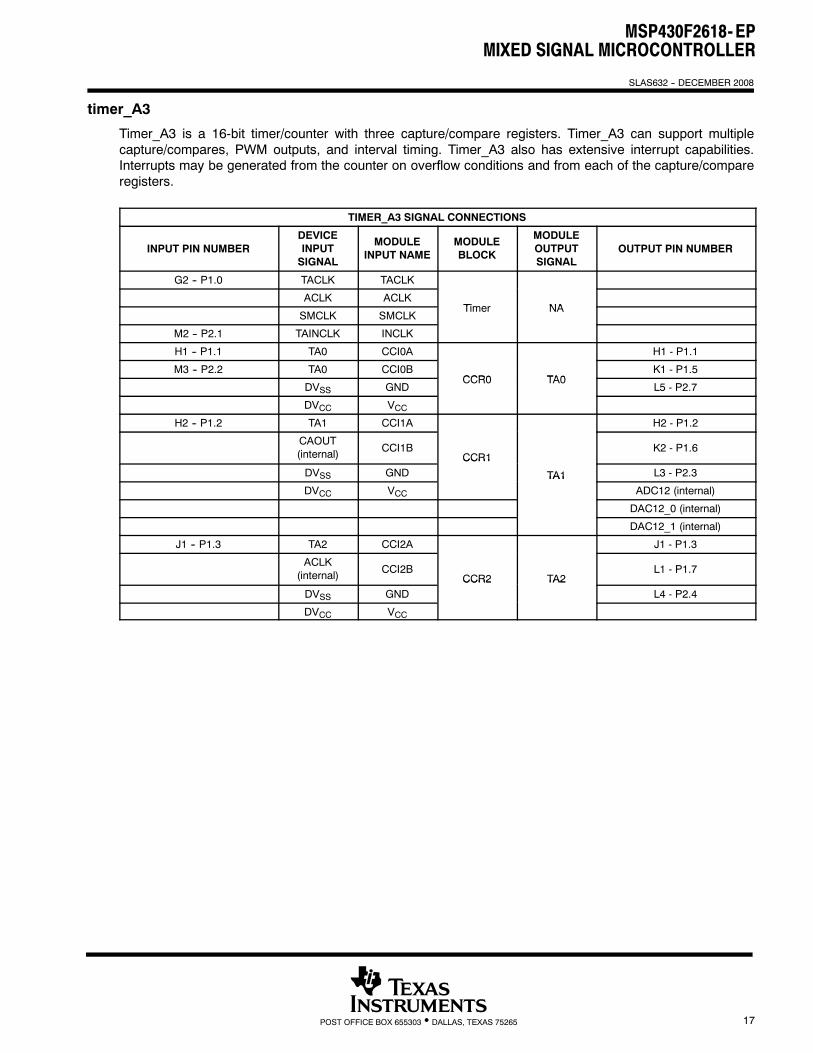
timer_A3
Timer_A3 is a 16-bit timer/counter with three capture/compare registers. Timer_A3 can support multiplecapture/compares, PWM outputs, and interval timing. Timer_A3 also has extensive interrupt capabilities.Interrupts may be generated from the counter on overflow conditions and from each of the capture/compareregisters.
TIMER_A3 SIGNAL CONNECTIONS
INPUT PIN NUMBERDEVICEINPUTSIGNAL
MODULEINPUT NAME
MODULEBLOCK
MODULEOUTPUTSIGNAL
OUTPUT PIN NUMBER
G2 -- P1.0 TACLK TACLK
ACLK ACLKTimer NA
SMCLK SMCLKTimer NA
M2 -- P2.1 TAINCLK INCLK
H1 -- P1.1 TA0 CCI0A H1 - P1.1
M3 -- P2.2 TA0 CCI0BCCR0 TA0
K1 - P1.5
DVSS GNDCCR0 TA0
L5 - P2.7
DVCC VCCH2 -- P1.2 TA1 CCI1A H2 - P1.2
CAOUT(internal) CCI1B
CCR1K2 - P1.6
DVSS GNDCCR1
TA1 L3 - P2.3
DVCC VCC
TA1ADC12 (internal)
DAC12_0 (internal)
DAC12_1 (internal)
J1 -- P1.3 TA2 CCI2A J1 - P1.3
ACLK(internal) CCI2B
CCR2 TA2L1 - P1.7
DVSS GNDCCR2 TA2
L4 - P2.4
DVCC VCC

MSP430F2618-EPMIXED SIGNAL MICROCONTROLLER
SLAS632 -- DECEMBER 2008
18 POST OFFICE BOX 655303 DALLAS, TEXAS 75265
timer_B7
Timer_B7 is a 16-bit timer/counter with seven capture/compare registers. Timer_B7 can support multiplecapture/compares, PWM outputs, and interval timing. Timer_B7 also has extensive interrupt capabilities.Interrupts may be generated from the counter on overflow conditions and from each of the capture/compareregisters.
TIMER_B3/B7 SIGNAL CONNECTIONS†
INPUT PIN NUMBERDEVICEINPUTSIGNAL
MODULEINPUT NAME
MODULEBLOCK
MODULEOUTPUTSIGNAL
OUTPUT PIN NUMBER
K11 -- P4.7 TBCLK TBCLK
ACLK ACLKTimer NA
SMCLK SMCLKTimer NA
K11 -- P4.7 TBCLK INCLK
M9 -- P4.0 TB0 CCI0A M9 - P4.0
M9-- P4.0 TB0 CCI0BCCR0 TB0
ADC12 (internal)
DVSS GNDCCR0 TB0
DVCC VCCJ9 -- P4.1 TB1 CCI1A J9 - P4.1
J9 -- P4.1 TB1 CCI1BCCR1 TB1
ADC12 (internal)
DVSS GNDCCR1 TB1
DVCC VCCM10 -- P4.2 TB2 CCI2A M10 - P4.2
M10 -- P4.2 TB2 CCI2BCCR2 TB2
DAC_0(internal)
DVSS GNDCCR2 TB2
DAC_1(internal)
DVCC VCCL10 -- P4.3 TB3 CCI3A L10 - P4.3
L10 -- P4.3 TB3 CCI3BCCR3 TB3
DVSS GNDCCR3 TB3
DVCC VCCM11 -- P4.4 TB4 CCI4A M11 - P4.4
M11 -- P4.4 TB4 CCI4BCCR4 TB4
DVSS GNDCCR4 TB4
DVCC VCCM12 -- P4.5 TB5 CCI5A M12 - P4.5
M12 -- P4.5 TB5 CCI5BCCR5 TB5
DVSS GNDCCR5 TB5
DVCC VCCL12 -- P4.6 TB6 CCI6A L12 - P4.6
ACLK(internal)
CCI6B
CCR6 TB6DVSS GND
CCR6 TB6
DVCC VCC

MSP430F2618-EPMIXED SIGNAL MICROCONTROLLER
SLAS632 -- DECEMBER 2008
19POST OFFICE BOX 655303 DALLAS, TEXAS 75265
comparator_A+
The primary function of the comparator_A+ module is to support precision slope analog-to-digital conversions,battery-voltage supervision, and monitoring of external analog signals.
ADC12The ADC12 module supports fast 12-bit analog-to-digital conversions. The module implements a 12-bit SARcore, sample select control, reference generator, and a 16-word conversion-and-control buffer. Theconversion-and-control buffer allows up to 16 independent ADC samples to be converted and stored withoutany CPU intervention.
DAC12
The DAC12 module is a 12-bit, R-ladder, voltage-output digital-to-analog converter (DAC). The DAC12 may beused in 8-bit or 12-bit mode and may be used in conjunction with the DMA controller. When multiple DAC12modules are present, they may be grouped together for synchronous operation.
MSP430F2618-EPMIXED SIGNAL MICROCONTROLLER
SLAS632 -- DECEMBER 2008
20 POST OFFICE BOX 655303 DALLAS, TEXAS 75265
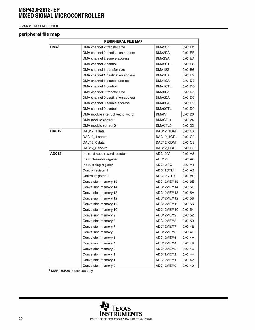
peripheral file mapPERIPHERAL FILE MAP
DMA† DMA channel 2 transfer size DMA2SZ 0x01F2
DMA channel 2 destination address DMA2DA 0x01EE
DMA channel 2 source address DMA2SA 0x01EA
DMA channel 2 control DMA2CTL 0x01E8
DMA channel 1 transfer size DMA1SZ 0x01E6
DMA channel 1 destination address DMA1DA 0x01E2
DMA channel 1 source address DMA1SA 0x01DE
DMA channel 1 control DMA1CTL 0x01DC
DMA channel 0 transfer size DMA0SZ 0x01DA
DMA channel 0 destination address DMA0DA 0x01D6
DMA channel 0 source address DMA0SA 0x01D2
DMA channel 0 control DMA0CTL 0x01D0
DMA module interrupt vector word DMAIV 0x0126
DMA module control 1 DMACTL1 0x0124
DMA module control 0 DMACTL0 0x0122
DAC12† DAC12_1 data DAC12_1DAT 0x01CA
DAC12_1 control DAC12_1CTL 0x01C2
DAC12_0 data DAC12_0DAT 0x01C8
DAC12_0 control DAC12_0CTL 0x01C0
ADC12 Interrupt-vector-word register ADC12IV 0x01A8
Inerrupt-enable register ADC12IE 0x01A6
Inerrupt-flag register ADC12IFG 0x01A4
Control register 1 ADC12CTL1 0x01A2
Control register 0 ADC12CTL0 0x01A0
Conversion memory 15 ADC12MEM15 0x015E
Conversion memory 14 ADC12MEM14 0x015C
Conversion memory 13 ADC12MEM13 0x015A
Conversion memory 12 ADC12MEM12 0x0158
Conversion memory 11 ADC12MEM11 0x0156
Conversion memory 10 ADC12MEM10 0x0154
Conversion memory 9 ADC12MEM9 0x0152
Conversion memory 8 ADC12MEM8 0x0150
Conversion memory 7 ADC12MEM7 0x014E
Conversion memory 6 ADC12MEM6 0x014C
Conversion memory 5 ADC12MEM5 0x014A
Conversion memory 4 ADC12MEM4 0x0148
Conversion memory 3 ADC12MEM3 0x0146
Conversion memory 2 ADC12MEM2 0x0144
Conversion memory 1 ADC12MEM1 0x0142
Conversion memory 0 ADC12MEM0 0x0140† MSP430F261x devices only

MSP430F2618-EPMIXED SIGNAL MICROCONTROLLER
SLAS632 -- DECEMBER 2008
21POST OFFICE BOX 655303 DALLAS, TEXAS 75265
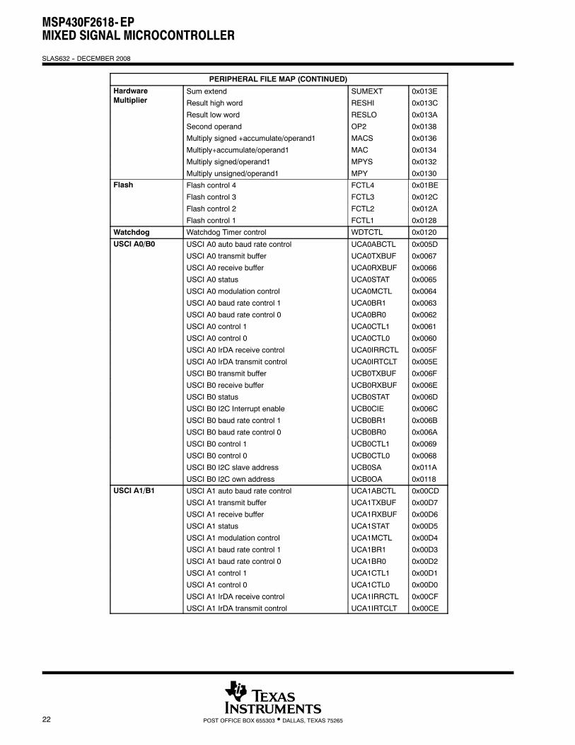
PERIPHERAL FILE MAP (CONTINUED)
ADC12 ADC memory-control register15 ADC12MCTL15 0x008F(continued) ADC memory-control register14 ADC12MCTL14 0x008E
ADC memory-control register13 ADC12MCTL13 0x008D
ADC memory-control register12 ADC12MCTL12 0x008C
ADC memory-control register11 ADC12MCTL11 0x008B
ADC memory-control register10 ADC12MCTL10 0x008A
ADC memory-control register9 ADC12MCTL9 0x0089
ADC memory-control register8 ADC12MCTL8 0x0088
ADC memory-control register7 ADC12MCTL7 0x0087
ADC memory-control register6 ADC12MCTL6 0x0086
ADC memory-control register5 ADC12MCTL5 0x0085
ADC memory-control register4 ADC12MCTL4 0x0084
ADC memory-control register3 ADC12MCTL3 0x0083
ADC memory-control register2 ADC12MCTL2 0x0082
ADC memory-control register1 ADC12MCTL1 0x0081
ADC memory-control register0 ADC12MCTL0 0x0080Timer_B7 Capture/compare register 6 TBCCR6 0x019E_
Capture/compare register 5 TBCCR5 0x019C
Capture/compare register 4 TBCCR4 0x019A
Capture/compare register 3 TBCCR3 0x0198
Capture/compare register 2 TBCCR2 0x0196
Capture/compare register 1 TBCCR1 0x0194
Capture/compare register 0 TBCCR0 0x0192
Timer_B register TBR 0x0190
Capture/compare control 6 TBCCTL6 0x018E
Capture/compare control 5 TBCCTL5 0x018C
Capture/compare control 4 TBCCTL4 0x018A
Capture/compare control 3 TBCCTL3 0x0188
Capture/compare control 2 TBCCTL2 0x0186
Capture/compare control 1 TBCCTL1 0x0184
Capture/compare control 0 TBCCTL0 0x0182
Timer_B control TBCTL 0x0180
Timer_B interrupt vector TBIV 0x011ETimer_A3 Capture/compare register 2 TACCR2 0x0176_
Capture/compare register 1 TACCR1 0x0174
Capture/compare register 0 TACCR0 0x0172
Timer_A register TAR 0x0170
Reserved 0x016E
Reserved 0x016C
Reserved 0x016A
Reserved 0x0168
Capture/compare control 2 TACCTL2 0x0166
Capture/compare control 1 TACCTL1 0x0164
Capture/compare control 0 TACCTL0 0x0162
Timer_A control TACTL 0x0160
Timer_A interrupt vector TAIV 0x012E
MSP430F2618-EPMIXED SIGNAL MICROCONTROLLER
SLAS632 -- DECEMBER 2008
22 POST OFFICE BOX 655303 DALLAS, TEXAS 75265
PERIPHERAL FILE MAP (CONTINUED)
Hardware Sum extend SUMEXT 0x013EMultiplier Result high word RESHI 0x013C
Result low word RESLO 0x013A
Second operand OP2 0x0138
Multiply signed +accumulate/operand1 MACS 0x0136
Multiply+accumulate/operand1 MAC 0x0134
Multiply signed/operand1 MPYS 0x0132
Multiply unsigned/operand1 MPY 0x0130Flash Flash control 4 FCTL4 0x01BE
Flash control 3 FCTL3 0x012C
Flash control 2 FCTL2 0x012A
Flash control 1 FCTL1 0x0128
Watchdog Watchdog Timer control WDTCTL 0x0120
USCI A0/B0 USCI A0 auto baud rate control UCA0ABCTL 0x005D/
USCI A0 transmit buffer UCA0TXBUF 0x0067
USCI A0 receive buffer UCA0RXBUF 0x0066
USCI A0 status UCA0STAT 0x0065
USCI A0 modulation control UCA0MCTL 0x0064
USCI A0 baud rate control 1 UCA0BR1 0x0063
USCI A0 baud rate control 0 UCA0BR0 0x0062
USCI A0 control 1 UCA0CTL1 0x0061
USCI A0 control 0 UCA0CTL0 0x0060
USCI A0 IrDA receive control UCA0IRRCTL 0x005F
USCI A0 IrDA transmit control UCA0IRTCLT 0x005E
USCI B0 transmit buffer UCB0TXBUF 0x006F
USCI B0 receive buffer UCB0RXBUF 0x006E
USCI B0 status UCB0STAT 0x006D
USCI B0 I2C Interrupt enable UCB0CIE 0x006C
USCI B0 baud rate control 1 UCB0BR1 0x006B
USCI B0 baud rate control 0 UCB0BR0 0x006A
USCI B0 control 1 UCB0CTL1 0x0069
USCI B0 control 0 UCB0CTL0 0x0068
USCI B0 I2C slave address UCB0SA 0x011A
USCI B0 I2C own address UCB0OA 0x0118USCI A1/B1 USCI A1 auto baud rate control UCA1ABCTL 0x00CD/
USCI A1 transmit buffer UCA1TXBUF 0x00D7
USCI A1 receive buffer UCA1RXBUF 0x00D6
USCI A1 status UCA1STAT 0x00D5
USCI A1 modulation control UCA1MCTL 0x00D4
USCI A1 baud rate control 1 UCA1BR1 0x00D3
USCI A1 baud rate control 0 UCA1BR0 0x00D2
USCI A1 control 1 UCA1CTL1 0x00D1
USCI A1 control 0 UCA1CTL0 0x00D0
USCI A1 IrDA receive control UCA1IRRCTL 0x00CF
USCI A1 IrDA transmit control UCA1IRTCLT 0x00CE

MSP430F2618-EPMIXED SIGNAL MICROCONTROLLER
SLAS632 -- DECEMBER 2008
23POST OFFICE BOX 655303 DALLAS, TEXAS 75265
PERIPHERAL FILE MAP (CONTINUED)
USCI A1/B1 USCI B1 transmit buffer UCB1TXBUF 0x00DF/(continued) USCI B1 receive buffer UCB1RXBUF 0x00DE
USCI B1 status UCB1STAT 0x00DD
USCI B1 I2C Interrupt enable UCB1CIE 0x00DC
USCI B1 baud rate control 1 UCB1BR1 0x00DB
USCI B1 baud rate control 0 UCB1BR0 0x00DA
USCI B1 control 1 UCB1CTL1 0x00D9
USCI B1 control 0 UCB1CTL0 0x00D8
USCI B1 I2C slave address UCB1SA 0x017E
USCI B1 I2C own address UCB1OA 0x017C
USCI A1/B1 interrupt enable UC1IE 0x0006
USCI A1/B1 interrupt flag UC1IFG 0x0007Comparator_A+ Comparator_A port disable CAPD 0x005Bp _
Comparator_A control2 CACTL2 0x005A
Comparator_A control1 CACTL1 0x0059Basic Clock Basic clock system control3 BCSCTL3 0x0053
Basic clock system control2 BCSCTL2 0x0058
Basic clock system control1 BCSCTL1 0x0057
DCO clock frequency control DCOCTL 0x0056
Brownout, SVS SVS control register (reset by brownout signal) SVSCTL 0x0055
Port PA Port PA resistor enable PAREN 0x0014
Port PA selection PASEL 0x003E
Port PA direction PADIR 0x003C
Port PA output PAOUT 0x003A
Port PA input PAIN 0x0038Port P8 Port P8 resistor enable P8REN 0x0015
Port P8 selection P8SEL 0x003F
Port P8 direction P8DIR 0x003D
Port P8 output P8OUT 0x003B
Port P8 input P8IN 0x0039Port P7 Port P7 resistor enable P7REN 0x0014
Port P7 selection P7SEL 0x003E
Port P7 direction P7DIR 0x003C
Port P7 output P7OUT 0x003A
Port P7 input P7IN 0x0038Port P6 Port P6 resistor enable P6REN 0x0013
Port P6 selection P6SEL 0x0037
Port P6 direction P6DIR 0x0036
Port P6 output P6OUT 0x0035
Port P6 input P6IN 0x0034Port P5 Port P5 resistor enable P5REN 0x0012
Port P5 selection P5SEL 0x0033
Port P5 direction P5DIR 0x0032
Port P5 output P5OUT 0x0031
Port P5 input P5IN 0x0030

MSP430F2618-EPMIXED SIGNAL MICROCONTROLLER
SLAS632 -- DECEMBER 2008
24 POST OFFICE BOX 655303 DALLAS, TEXAS 75265
PERIPHERAL FILE MAP (CONTINUED)
Port P4 Port P4 selection P4SEL 0x001F
Port P4 resistor enable P4REN 0x0011
Port P4 direction P4DIR 0x001E
Port P4 output P4OUT 0x001D
Port P4 input P4IN 0x001CPort P3 Port P3 resistor enable P3REN 0x0010
Port P3 selection P3SEL 0x001B
Port P3 direction P3DIR 0x001A
Port P3 output P3OUT 0x0019
Port P3 input P3IN 0x0018Port P2 Port P2 resistor enable P2REN 0x002F
Port P2 selection P2SEL 0x002E
Port P2 interrupt enable P2IE 0x002D
Port P2 interrupt-edge select P2IES 0x002C
Port P2 interrupt flag P2IFG 0x002B
Port P2 direction P2DIR 0x002A
Port P2 output P2OUT 0x0029
Port P2 input P2IN 0x0028Port P1 Port P1 resistor enable P1REN 0x0027
Port P1 selection P1SEL 0x0026
Port P1 interrupt enable P1IE 0x0025
Port P1 interrupt-edge select P1IES 0x0024
Port P1 interrupt flag P1IFG 0x0023
Port P1 direction P1DIR 0x0022
Port P1 output P1OUT 0x0021
Port P1 input P1IN 0x0020Special Functions SFR interrupt flag2 IFG2 0x0003p
SFR interrupt flag1 IFG1 0x0002
SFR interrupt enable2 IE2 0x0001
SFR interrupt enable1 IE1 0x0000

MSP430F2618-EPMIXED SIGNAL MICROCONTROLLER
SLAS632 -- DECEMBER 2008
25POST OFFICE BOX 655303 DALLAS, TEXAS 75265
absolute maximum ratings (see Note 1)Voltage applied at VCC to VSS --0.3 V to 4.1 V. . . . . . . . . . . . . . . . . . . . . . . . . . . . . . . . . . . . . . . . . . . . . . . . . . . . . .Voltage applied to any pin (see Note 2) --0.3 V to VCC + 0.3 V. . . . . . . . . . . . . . . . . . . . . . . . . . . . . . . . . . . . . . . .Diode current at any device terminal . 2 mA. . . . . . . . . . . . . . . . . . . . . . . . . . . . . . . . . . . . . . . . . . . . . . . . . . . . . .Storage temperature: Unprogrammed device (see Note 3) --55C to 150C. . . . . . . . . . . . . . . . . . . . . . . . . . .
Programmed device (see Note 3) --40C to 105C. . . . . . . . . . . . . . . . . . . . . . . . . . . . .NOTES: 1. Stresses beyond those listed under “absolute maximum ratings” may cause permanent damage to the device. These are stress
ratings only, and functional operation of the device at these or any other conditions beyond those indicated under “recommendedoperating conditions” is not implied. Exposure to absolute-maximum-rated conditions for extended periods may affect devicereliability.
2. All voltages referenced to VSS. The JTAG fuse-blow voltage, VFB, is allowed to exceed the absolute maximum rating. The voltageis applied to the TDI/TCLK pin when blowing the JTAG fuse.
3. Higher temperature may be applied during board soldering process according to the current JEDEC J-STD-020 specification, withpeak reflow temperatures not higher than classified on the device label on the shipping boxes or reels.
recommended operating conditionsPARAMETER MIN MAX UNIT
Supply voltage during program execution, VCC AVCC = DVCC = VCC (see Note 1) 1.8 3.6 V
Supply voltage during flash memory programming, VCC AVCC = DVCC = VCC (see Note 1) 2.2 3.6 V
Supply voltage, VSS AVSS = DVSS = VSS 0.0 0.0 V
Operating free air temperature TI version --40 85
COperating free-air temperature, TA T version --40 105C
VCC = 1.8 V,Duty cycle = 50% 10% dc 4.15
Processor frequency fSYSYTEM (maximum MCLK frequency)(see Notes 2 and 3 and Figure 1)
VCC = 2.7 V,Duty cycle = 50% 10% dc 12 MHz
VCC 3.3 V,Duty cycle = 50% 10% dc 16
NOTES: 1. It is recommended to power AVCC and DVCC from the same source. A maximum difference of 0.3 V between AVCC and DVCC canbe tolerated during power-up.
2. The MSP430 CPU is clocked directly with MCLK.Both the high and low phase of MCLK must not exceed the pulse width of the specified maximum frequency.
3. Modulesmight haveadifferentmaximum input clock specification. See the specification of the respectivemodule in this data sheet.
4.15 MHz
12 MHz
16 MHz
1.8 V 2.2 V 2.7 V 3.3 V 3.6 V
Supply Voltage --V
SystemFrequency--M
Hz
Supply voltage rangeduring flash memoryprogramming
Supply voltage rangeduring program execution
Legend:
7.5 MHz
NOTE: Minimum processor frequency is defined by system clock. Flash program or erase operations require a minimum VCC of 2.2 V.
Figure 1. Operating Area

MSP430F2618-EPMIXED SIGNAL MICROCONTROLLER
SLAS632 -- DECEMBER 2008
26 POST OFFICE BOX 655303 DALLAS, TEXAS 75265
electrical characteristics over recommended ranges of supply voltage and operating free-airtemperature (unless otherwise noted)
active mode supply current into VCC excluding external current (see Notes 1 and 2)
PARAMETER TEST CONDITIONS TA VCC MIN TYP MAX UNIT
fDCO = fMCLK = fSMCLK = 1 MHz,fACLK = 32 768 Hz
--40_C to 85_C2 2 V
365 395
I Active mode (AM)
fACLK = 32,768 Hz,Program executes from flash,BCSCTL1 CALBC1 1MHZ
105_C2.2 V
375 420AIAM, 1MHz
Active mode (AM)current (1 MHz)
BCSCTL1 = CALBC1_1MHZ,DCOCTL = CALDCO_1MHZ,CPUOFF 0 SCG0 0 SCG1 0
--40_C to 85_C3 V
515 560A
_CPUOFF = 0, SCG0 = 0, SCG1 = 0,OSCOFF = 0 105_C
3 V525 595
fDCO = fMCLK = fSMCLK = 1 MHz,fACLK = 32 768 Hz
--40_C to 85_C2 2 V
330 370
I Active mode (AM)
fACLK = 32,768 Hz,Program executes in RAM,BCSCTL1 CALBC1 1MHZ
105_C2.2 V
340 390AIAM, 1MHz
Active mode (AM)current (1 MHz)
BCSCTL1 = CALBC1_1MHZ,DCOCTL = CALDCO_1MHZ,CPUOFF 0 SCG0 0 SCG1 0
--40_C to 85_C3 V
460 495A
_CPUOFF = 0, SCG0 = 0, SCG1 = 0,OSCOFF = 0 105_C
3 V470 520
fMCLK = fSMCLK =fACLK = 32,768 Hz/8 = 4,096 Hz,
--40_C to 85_C2 2 V
2.1 9
I Active mode (AM)
fACLK = 32,768 Hz/8 = 4,096 Hz,fDCO = 0 Hz,Program executes in flash,
105_C2.2 V
15 31AIAM, 4kHz
Active mode (AM)current (4 kHz)
Program executes in flash,SELMx = 11, SELS = 1,DIVMx = DIVSx = DIVAx = 11, --40_C to 85_C
3 V3 11
A
DIVMx DIVSx DIVAx 11,CPUOFF = 0, SCG0 = 1, SCG1 = 0,OSCOFF = 0 105_C
3 V19 32
fMCLK = fSMCLK = fDCO(0, 0) 100 kHz,f 0 Hz
--40_C to 85_C2 2 V
67 86
I Active mode (AM)fACLK = 0 Hz,Program executes in flash, 105_C
2.2 V80 99
AIAM,100kHzActive mode (AM)current (100 kHz)
Program executes in flash,RSELx = 0, DCOx = 0,CPUOFF = 0 SCG0 = 0 SCG1 = 0
--40_C to 85_C3 V
84 107A
CPUOFF = 0, SCG0 = 0, SCG1 = 0,OSCOFF = 1 105_C
3 V99 128
NOTES: 1. All inputs are tied to 0 V or VCC. Outputs do not source or sink any current.2. The currents are characterizedwith amicrocrystal CC4V-T1ASMDcrystalwith a load capacitanceof 9pF. The internal andexternal
load capacitance is chosen to closely match the required 9 pF.

MSP430F2618-EPMIXED SIGNAL MICROCONTROLLER
SLAS632 -- DECEMBER 2008
27POST OFFICE BOX 655303 DALLAS, TEXAS 75265
electrical characteristics over recommended ranges of supply voltage and operating free-airtemperature (unless otherwise noted)
typical characteristics -- active mode supply current (into DVCC + AVCC)
0.0
1.0
2.0
3.0
4.0
5.0
6.0
7.0
8.0
9.0
10.0
1.5 2.0 2.5 3.0 3.5 4.0
VCC -- Supply Voltage -- V
ActiveModeCurrent--mA
Figure 2. Active Mode Current vs VCC, TA = 25C
fDCO = 1 MHz
fDCO = 8 MHz
fDCO = 12 MHz
fDCO = 16 MHz
0.0
1.0
2.0
3.0
4.0
5.0
6.0
7.0
0.0 4.0 8.0 12.0 16.0
fDCO -- DCO Frequency -- MHz
ActiveModeCurrent--mA
Figure 3. Active Mode Current vs DCO Frequency
TA = 25 C
TA = 85 C
VCC = 2.2 V
VCC = 3 V
TA = 25 C
TA = 85 C

MSP430F2618-EPMIXED SIGNAL MICROCONTROLLER
SLAS632 -- DECEMBER 2008
28 POST OFFICE BOX 655303 DALLAS, TEXAS 75265
electrical characteristics over recommended ranges of supply voltage and operating free-airtemperature (unless otherwise noted)
low-power mode supply current into VCC excluding external current (see Notes 1 and 2)
PARAMETER TEST CONDITIONS TA VCC MIN TYP MAX UNIT
fMCLK = 0 MHz,fSMCLK = fDCO = 1 MHz
--40_C to 85_C2 2 V
68 83
ILow-power mode 0(LPM0) current
fSMCLK = fDCO = 1 MHz,fACLK = 32,768 Hz,BCSCTL1 CALBC1 1MHZ
105_C2.2 V
83 98AILPM0, 1MHz (LPM0) current,
see Note 3BCSCTL1 = CALBC1_1MHZ,DCOCTL = CALDCO_1MHZ,CPUOFF 1 SCG0 0 SCG1 0
--40_C to 85_C3 V
87 105A
_CPUOFF = 1, SCG0 = 0, SCG1 = 0,OSCOFF = 0 105_C
3 V100 125
fMCLK = 0MHz,f f 100 kHz
--40_C to 85_C2 2 V
37 49
ILPM0,Low-power mode 0(LPM0) current
fSMCLK = fDCO(0, 0) 100 kHz,fACLK = 0 Hz, 105_C
2.2 V50 62
AILPM0,100kHz
(LPM0) current,see Note 3
fACLK = 0 Hz,RSELx = 0, DCOx = 0,CPUOFF = 1 SCG0 = 0 SCG1 = 0
--40_C to 85_C3 V
40 55A
see Note 3 CPUOFF = 1, SCG0 = 0, SCG1 = 0,OSCOFF = 1 105_C
3 V57 73
fMCLK = fSMCLK = 0 MHz, fDCO = 1 MHz,f 32 768 Hz
--40_C to 85_C2 2 V
23 33
ILow-power mode 2(LPM2) current
fACLK = 32,768 Hz,BCSCTL1 = CALBC1_1MHZ, 105_C
2.2 V35 46
AILPM2 (LPM2) current,see Note 4
BCSCTL1 = CALBC1_1MHZ,DCOCTL = CALDCO_1MHZ,CPUOFF = 1 SCG0 = 0 SCG1 = 1
--40_C to 85_C3 V
25 36A
see Note 4 CPUOFF = 1, SCG0 = 0, SCG1 = 1,OSCOFF = 0 105_C
3 V40 55
--40C 0.8 1.2
25C2 2 V
1 1.3
fDCO = fMCLK = fSMCLK = 0 MHz85C
2.2 V4.6 7
ILow-power mode 3(LPM3) current
fDCO = fMCLK = fSMCLK = 0 MHz,fACLK = 32,768 Hz, 105C 14 24
AILPM3,LFXT1 (LPM3) current,see Note 4
fACLK = 32,768 Hz,CPUOFF = 1, SCG0 = 1, SCG1 = 1,OSCOFF 0
--40C 0.9 1.3A
see Note 4OSCOFF = 0 25C
3 V1.1 1.5
85C3 V
5.5 8
105C 17 30
--40C 0.4 1.0
25C2 2 V
0.5 1.0
fDCO = fMCLK = fSMCLK = 0 MHz85C
2.2 V4.3 6.5
I Low-power mode 3fDCO = fMCLK = fSMCLK = 0 MHz,fACLK from internal LF oscillator (VLO), 105C 14 24
AILPM3,VLOLow-power mode 3(LPM3) current,
N t 4
fACLK from internal LF oscillator (VLO),CPUOFF = 1, SCG0 = 1, SCG1 = 1,OSCOFF 0
--40C 0.6 1.2A
( )see Note 4 OSCOFF = 0 25C
3 V0.6 1.2
85C3 V
5 7.5
105C 16.5 29.5
NOTES: 1. All inputs are tied to 0 V or VCC. Outputs do not source or sink any current.2. The currents are characterizedwith amicrocrystal CC4V-T1ASMDcrystalwith a load capacitanceof 9pF. The internal andexternal
load capacitance is chosen to closely match the required 9 pF.3. Current for Brownout and WDT+ is included. The WDT+ is clocked by SMCLK.4. Current for Brownout and WDT+ is included. The WDT+ is clocked by ACLK.

MSP430F2618-EPMIXED SIGNAL MICROCONTROLLER
SLAS632 -- DECEMBER 2008
29POST OFFICE BOX 655303 DALLAS, TEXAS 75265
electrical characteristics over recommended ranges of supply voltage and operating free-airtemperature (unless otherwise noted)
low-power mode supply current into VCC excluding external current (see Notes 1 and 2) (continued)
PARAMETER TEST CONDITIONS TA VCC MIN TYP MAX UNIT
Low-power mode 4 fDCO = fMCLK = fSMCLK = 0 MHz--40C 0.1 0.5
I
Low-power mode 4(LPM4) current,
fDCO = fMCLK = fSMCLK = 0 MHz,fACLK = 0 Hz, 25C
2 2 V0.1 0.5
AILPM4(LPM4) current,see Note 3
fACLK = 0 Hz,CPUOFF = 1, SCG0 = 1, SCG1 = 1,OSCOFF 1
85C2.2 V
4 6A
OSCOFF = 1105C 13 23
Low-power mode 4 fDCO = fMCLK = fSMCLK = 0 MHz--40C 0.2 0.5
I
Low-power mode 4(LPM4) current,
fDCO = fMCLK = fSMCLK = 0 MHz,fACLK = 0 Hz, 25C
3 V0.2 0.5
AILPM4(LPM4) current,see Note 3
fACLK = 0 Hz,CPUOFF = 1, SCG0 = 1, SCG1 = 1,OSCOFF 1
85C3 V
4.7 7A
OSCOFF = 1105C 14 24
NOTES: 1. All inputs are tied to 0 V or VCC. Outputs do not source or sink any current.2. Thecurrents arecharacterizedwithamicrocrystal CC4V--T1ASMDcrystalwith a load capacitanceof 9pf. The internal andexternal
load capacitance is chosen to closely match the required 9 pf.3. Current for Brownout included.
typical characteristics -- LPM4 current
0.01.02.03.04.05.06.07.08.09.010.011.012.013.014.015.016.0
--40.0 --20.0 0.0 20.0 40.0 60.0 80.0 100.0 120.0
TA -- Temperature -- C
ILPM4--Low--power
modecurrent--uA
Vcc = 3.6V
TA -- Temperature -- C
ILPM4--Low--power
modecurrent--
Vcc = 1.8V
Vcc = 3.0V
Vcc = 2.2V
Figure 4. ILPM4 -- LPM4 Current vs. Temperature

MSP430F2618-EPMIXED SIGNAL MICROCONTROLLER
SLAS632 -- DECEMBER 2008
30 POST OFFICE BOX 655303 DALLAS, TEXAS 75265
Schmitt-trigger inputs -- ports P1 through P8, RST/NMI, JTAG, XIN, and XT2IN (see Note 1)PARAMETER TEST CONDITIONS VCC MIN TYP MAX UNIT
0.45 VCC 0.75 VCC
VIT+ Positive-going input threshold voltage 2.2 V 1.0 1.65 VVIT+ Positive going input threshold voltage
3 V 1.35 2.25
V
0.25 VCC 0.55 VCC
VIT-- Negative-going input threshold voltage 2.2 V 0.55 1.2 VVIT-- Negative going input threshold voltage
3 V 0.75 1.65
V
V Input voltage hysteresis (V V )2.2 V 0.2 1.0
VVhys Input voltage hysteresis (VIT+ -- VIT--)3 V 0.3 1.0
V
RPull Pullup/pulldown resistor Pullup: VIN = VSS,Pulldown: VIN = VCC
20 35 50 kΩ
CI Input capacitance VIN = VSS or VCC 5 pF
NOTE 1: XIN and XT2IN in bypass mode only.
inputs -- ports P1 and P2PARAMETER TEST CONDITIONS VCC MIN MAX UNIT
tint External interrupt timingPort P1, P2: P1.x to P2.x, external trigger pulse width toset the interrupt flag (see Note 1) 2.2 V/3 V 20 ns
NOTE 1: The external signal sets the interrupt flag every time the minimum t(int) parameters are met. It may be set with trigger signals shorterthan t(int).
leakage current -- ports P1 through P8 (see Note 1 and 2)PARAMETER TEST CONDITIONS VCC MIN MAX UNIT
Ilkg (Px.x) High-impedance leakage current see Notes 1 and 2 2.2 V/3 V 50 nA
NOTES: 1. The leakage current is measured with VSS or VCC applied to the corresponding pin(s), unless otherwise noted.2. The leakageof digital port pins ismeasured individually. Theport pin is selected for input and thepullup/pulldown resistor isdisabled.

MSP430F2618-EPMIXED SIGNAL MICROCONTROLLER
SLAS632 -- DECEMBER 2008
31POST OFFICE BOX 655303 DALLAS, TEXAS 75265
electrical characteristics over recommended ranges of supply voltage and operating free-airtemperature (unless otherwise noted) (continued)
standard inputs -- RST/NMIPARAMETER TEST CONDITIONS VCC MIN MAX UNIT
VIL Low-level input voltage 2.2 V/3 V VSS VSS+0.6 V
VIH High-level input voltage 2.2 V/3 V 0.8VCC VCC V
outputs -- ports P1 through P8PARAMETER TEST CONDITIONS VCC MIN MAX UNIT
IOH(max) = --1.5 mA (see Note 1)2 2 V
VCC--0.25 VCC
V High level output voltageIOH(max) = --6 mA (see Note 2)
2.2 VVCC--0.6 VCC
VVOH High-level output voltageIOH(max) = --1.5 mA (see Note 1)
3 VVCC--0.25 VCC
V
IOH(max) = --6 mA (see Note 2)3 V
VCC--0.6 VCCIOL(max) = 1.5 mA (see Note 1)
2 2 VVSS VSS+0.25
V Low level output voltageIOL(max) = 6 mA (see Note 2)
2.2 VVSS VSS+0.6
VVOL Low-level output voltageIOL(max) = 1.5 mA (see Note 1)
3 VVSS VSS+0.25
V
IOL(max) = 6 mA (see Note 2)3 V
VSS VSS+0.6
NOTES: 1. The maximum total current, IOH(max) and IOL(max), for all outputs combined, should not exceed 12 mA to satisfy the maximumvoltage drop specified.
2. The maximum total current, IOH(max) and IOL(max), for all outputs combined, should not exceed 48 mA to satisfy the maximumvoltage drop specified.
output frequency -- ports P1 through P8PARAMETER TEST CONDITIONS VCC MIN TYP MAX UNIT
fPort output frequency P1.4/SMCLK, CL = 20 pF, RL = 1 kΩ 2.2 V DC 10
MHzfPx.yPort output frequencywith load
P1.4/SMCLK, CL 20 pF, RL 1 kΩ(see Notes 1 and 2) 3.0 V DC 12
MHz
f Clock output frequencyP2.0/ACLK/CA2, P1.4/SMCLK, CL = 20 pF 2.2 V DC 12
MHzfPort_CLK Clock output frequencyP2.0/ACLK/CA2, P1.4/SMCLK, CL 20 pF(see Note 2) 3.3 V DC 16
MHz
P5.6/ACLK, CL = 20 pF, LF mode 30 50 70
P5.6/ACLK, CL = 20 pF, XT1 mode 40 50 60 %
tDuty cycle of output P5.4/MCLK, CL = 20 pF, XT1 mode 40 60
%
t(Xdc)Duty cycle of outputfrequency P5.4/MCLK, CL = 20 pF, DCO 50% -- 15 ns 50 50% + 15 nsq y
P1.4/SMCLK, CL = 20 pF, XT2 mode 40 60 %
P1.4/SMCLK, CL = 20 pF, DCO 50% -- 15 ns 50% + 15 ns
NOTES: 1. A resistive divider with 2 times 0.5 kΩ betweenVCC andVSS is used as load. The output is connected to the center tap of the divider.2. The output voltage reaches at least 10% and 90% VCC at the specified toggle frequency.

MSP430F2618-EPMIXED SIGNAL MICROCONTROLLER
SLAS632 -- DECEMBER 2008
32 POST OFFICE BOX 655303 DALLAS, TEXAS 75265
electrical characteristics over recommended ranges of supply voltage and operating free-airtemperature (unless otherwise noted) (continued)
typical characteristics -- outputs
Figure 5
VOL -- Low-Level Output Voltage -- V
0.0
5.0
10.0
15.0
20.0
25.0
0.0 0.5 1.0 1.5 2.0 2.5
VCC = 2.2 VP4.5
TYPICAL LOW-LEVEL OUTPUT CURRENTvs
LOW-LEVEL OUTPUT VOLTAGEof one pin
TA = 25C
TA = 85C
OL
I--TypicalLow-LevelOutputCurrent--mA
Figure 6VOL -- Low-Level Output Voltage -- V
0.0
10.0
20.0
30.0
40.0
50.0
0.0 0.5 1.0 1.5 2.0 2.5 3.0 3.5
VCC = 3 VP4.5
TYPICAL LOW-LEVEL OUTPUT CURRENTvs
LOW-LEVEL OUTPUT VOLTAGEof one pin
TA = 25C
TA = 85C
OL
I--TypicalLow-LevelOutputCurrent--mA
Figure 7
VOH -- High-Level Output Voltage -- V
--25.0
--20.0
--15.0
--10.0
--5.0
0.0
0.0 0.5 1.0 1.5 2.0 2.5
VCC = 2.2 VP4.5
TYPICAL HIGH-LEVEL OUTPUT CURRENTvs
HIGH-LEVEL OUTPUT VOLTAGEof one pin
TA = 25C
TA = 85C
OH
I--TypicalHigh-LevelOutputCurrent--mA
Figure 8VOH -- High-Level Output Voltage -- V
--50.0
--40.0
--30.0
--20.0
--10.0
0.0
0.0 0.5 1.0 1.5 2.0 2.5 3.0 3.5
VCC = 3 VP4.5
TYPICAL HIGH-LEVEL OUTPUT CURRENTvs
HIGH-LEVEL OUTPUT VOLTAGEof one pin
TA = 25C
TA = 85C
OH
I--TypicalHigh-LevelOutputCurrent--mA

MSP430F2618-EPMIXED SIGNAL MICROCONTROLLER
SLAS632 -- DECEMBER 2008
33POST OFFICE BOX 655303 DALLAS, TEXAS 75265
electrical characteristics over recommended ranges of supply voltage and operating free-airtemperature (unless otherwise noted) (continued)
POR/brownout reset (BOR) (see Notes 1 and 2)PARAMETER TEST CONDITIONS VCC MIN TYP MAX UNIT
VCC(start) operating voltage dVCC/dt± 3 V/s 0.7¢ V(B_IT--) V
V(B_IT--) negative going VCC reset threshold voltage dVCC/dt± 3 V/s 1.71 V
Vhys(B_IT--) VCC reset threshold hysteresis dVCC/dt± 3 V/s 70 130 210 mV
td(BOR) BOR reset release delay time 2000 s
treset Pulse length at RST/NMI pin to accept a reset 2.2 V / 3 V 2 s
NOTES: 1. The current consumption of the brownout module is included in the ICC current consumption data. The voltage levelV(B_IT--) + Vhys(B_IT--) is 1.8 V.
2. During power up, the CPU begins code execution following a period of td(BOR) after VCC = V(B_IT--) + Vhys(B_IT--). The default DCOsettings must not be changed until VCC VCC(MIN), where VCC(min) is the minimum supply voltage for the desired operatingfrequency.
VCC
VCC(Start)
V(B_IT-)
Vhys(B_IT-)
1
0td(BOR)
Figure 9. POR/Brownout Reset (BOR) vs Supply Voltage

MSP430F2618-EPMIXED SIGNAL MICROCONTROLLER
SLAS632 -- DECEMBER 2008
34 POST OFFICE BOX 655303 DALLAS, TEXAS 75265
electrical characteristics over recommended ranges of supply voltage and operating free-airtemperature (unless otherwise noted) (continued)
typical characteristics -- POR/brownout reset (BOR)
VCC(drop)
VCC3 V
tpw
0
0.5
1
1.5
2
0.001 1 1000
Typical Conditions
1 ns 1 nstpw -- Pulse Width -- s
VCC(drop)--V
tpw -- Pulse Width -- s
VCC = 3 V
Figure 10. VCC(drop) Level With a Square Voltage Drop to Generate a POR/Brownout SignalVCC
0
0.5
1
1.5
2
VCC(drop)
tpw
tpw -- Pulse Width -- s
VCC(drop)--
V
3 V
0.001 1 1000 tf trtpw -- Pulse Width -- s
tf = tr
Typical Conditions
VCC = 3 V
Figure 11. VCC(drop) Level With a Triangle Voltage Drop to Generate a POR/Brownout Signal

MSP430F2618-EPMIXED SIGNAL MICROCONTROLLER
SLAS632 -- DECEMBER 2008
35POST OFFICE BOX 655303 DALLAS, TEXAS 75265
electrical characteristics over recommended ranges of supply voltage and operating free-airtemperature (unless otherwise noted) (continued)
SVS (supply voltage supervisor/monitor)PARAMETER TEST CONDITIONS MIN TYP MAX UNIT
tdVCC/dt > 30 V/ms (see Figure 12) 5 150
st(SVSR) dVCC/dt 30 V/ms 2000s
td(SVSon) SVSON, switch from VLD = 0 to VLD 0, VCC = 3 V 20 150 s
tsettle VLD 0‡ 12 s
V(SVSstart) VLD 0, VCC/dt 3 V/s (see Figure 12) 1.55 1.7 V
VLD = 1 70 120 210 mV
Vhys(SVS IT--)
VCC/dt 3 V/s (see Figure 12) VLD = 2 to 14V(SVS_IT--)
0.004V(SVS_IT--)
0.016 VVhys(SVS_IT--)
VCC/dt 3 V/s (see Figure 12),External voltage applied on A7 VLD = 15 4.4 20 mV
VLD = 1 1.8 1.9 2.05
VLD = 2 1.94 2.1 2.25
VLD = 3 2.05 2.2 2.37
VLD = 4 2.14 2.3 2.48
VLD = 5 2.24 2.4 2.6
VLD = 6 2.33 2.5 2.71
V /dt 3 V/s (see Figure 12 and Figure 13)VLD = 7 2.46 2.65 2.86
V(SVS IT )
VCC/dt 3 V/s (see Figure 12 and Figure 13) VLD = 8 2.58 2.8 3VV(SVS_IT--)
VLD = 9 2.69 2.9 3.13V
VLD = 10 2.83 3.05 3.29
VLD = 11 2.94 3.2 3.42
VLD = 12 3.11 3.35 3.61†
VLD = 13 3.24 3.5 3.76†
VLD = 14 3.43 3.7† 3.99†
VCC/dt 3 V/s (see Figure 12 and Figure 13),External voltage applied on A7 VLD = 15 1.1 1.2 1.3
ICC(SVS)(see Note 1) VLD 0, VCC = 2.2 V/3 V 10 15 A
† The recommended operating voltage range is limited to 3.6 V.‡ tsettle is the settling time that the comparator o/p needs to have a stable level after VLD is switched VLD 0 to a different VLD value between2 and 15. The overdrive is assumed to be > 50 mV.
NOTE 1: The current consumption of the SVS module is not included in the ICC current consumption data.

MSP430F2618-EPMIXED SIGNAL MICROCONTROLLER
SLAS632 -- DECEMBER 2008
36 POST OFFICE BOX 655303 DALLAS, TEXAS 75265
typical characteristics
VCC(start)
AVCC
V(B_IT--)
BrownoutRegion
V(SVSstart)
V(SVS_IT--)
Software sets VLD >0:SVS is active
td(SVSR)
undefined
Vhys(SVS_IT--)
0
1
td(BOR)
Brownout
0
1
td(SVSon)
td(BOR)
0
1Set POR
Brown-outRegion
SVS Circuit is Active From VLD > to VCC < V(B_IT--)SVS out
Vhys(B_IT--)
Figure 12. SVS Reset (SVSR) vs Supply Voltage
0
0.5
1
1.5
2
VCC
VCC
1 ns 1 ns
VCC(min)
tpw
tpw -- Pulse Width -- s
VCC(m
in)--V
3 V
1 10 1000
tf trt -- Pulse Width -- s
100
tpw3 V
tf = tr
Rectangular Drop
Triangular Drop
VCC(min)
Figure 13. VCC(min): Square Voltage Drop and Triangle Voltage Drop to Generate an SVS Signal (VLD = 1)

MSP430F2618-EPMIXED SIGNAL MICROCONTROLLER
SLAS632 -- DECEMBER 2008
37POST OFFICE BOX 655303 DALLAS, TEXAS 75265
electrical characteristics over recommended ranges of supply voltage and operating free-airtemperature (unless otherwise noted) (continued)
main DCO characteristicsD All ranges selected by RSELx overlap with RSELx + 1: RSELx = 0 overlaps RSELx = 1, ... RSELx = 14
overlaps RSELx = 15.D DCO control bits DCOx have a step size as defined by parameter SDCO.D Modulation control bits MODx select how often fDCO(RSEL,DCO+1) is used within the period of 32 DCOCLK
cycles. The frequency fDCO(RSEL,DCO) is used for the remaining cycles. The frequency is an average equalto:
faverage=32× fDCO(RSEL,DCO)× fDCO(RSEL,DCO+1)
MOD× fDCO(RSEL,DCO)+(32−MOD)× fDCO(RSEL,DCO+1)
DCO frequencyPARAMETER TEST CONDITIONS VCC MIN TYP MAX UNIT
RSELx < 14 1.8 3.6
VCC Supply voltage RSELx = 14 2.2 3.6 VVCC Supply voltage
RSELx = 15 3.0 3.6
V
fDCO(0,0) DCO frequency (0, 0) RSELx = 0, DCOx = 0, MODx = 0 2.2 V/3 V 0.06 0.14 MHz
fDCO(0,3) DCO frequency (0, 3) RSELx = 0, DCOx = 3, MODx = 0 2.2 V/3 V 0.07 0.17 MHz
fDCO(1,3) DCO frequency (1, 3) RSELx = 1, DCOx = 3, MODx = 0 2.2 V/3 V 0.10 0.20 MHz
fDCO(2,3) DCO frequency (2, 3) RSELx = 2, DCOx = 3, MODx = 0 2.2 V/3 V 0.14 0.28 MHz
fDCO(3,3) DCO frequency (3, 3) RSELx = 3, DCOx = 3, MODx = 0 2.2 V/3 V 0.20 0.40 MHz
fDCO(4,3) DCO frequency (4, 3) RSELx = 4, DCOx = 3, MODx = 0 2.2 V/3 V 0.28 0.54 MHz
fDCO(5,3) DCO frequency (5, 3) RSELx = 5, DCOx = 3, MODx = 0 2.2 V/3 V 0.39 0.77 MHz
fDCO(6,3) DCO frequency (6, 3) RSELx = 6, DCOx = 3, MODx = 0 2.2 V/3 V 0.54 1.06 MHz
fDCO(7,3) DCO frequency (7, 3) RSELx = 7, DCOx = 3, MODx = 0 2.2 V/3 V 0.80 1.50 MHz
fDCO(8,3) DCO frequency (8, 3) RSELx = 8, DCOx = 3, MODx = 0 2.2 V/3 V 1.10 2.10 MHz
fDCO(9,3) DCO frequency (9, 3) RSELx = 9, DCOx = 3, MODx = 0 2.2 V/3 V 1.60 3.00 MHz
fDCO(10,3) DCO frequency (10, 3) RSELx = 10, DCOx = 3, MODx = 0 2.2 V/3 V 2.50 4.30 MHz
fDCO(11,3) DCO frequency (11, 3) RSELx = 11, DCOx = 3, MODx = 0 2.2 V/3 V 3.00 5.50 MHz
fDCO(12,3) DCO frequency (12, 3) RSELx = 12, DCOx = 3, MODx = 0 2.2 V/3 V 4.30 7.30 MHz
fDCO(13,3) DCO frequency (13, 3) RSELx = 13, DCOx = 3, MODx = 0 2.2 V/3 V 6.00 9.60 MHz
fDCO(14,3) DCO frequency (14, 3) RSELx = 14, DCOx = 3, MODx = 0 2.2 V/3 V 8.60 13.9 MHz
fDCO(15,3) DCO frequency (15, 3) RSELx = 15, DCOx = 3, MODx = 0 3 V 12.0 18.5 MHz
fDCO(15,7) DCO frequency (15, 7) RSELx = 15, DCOx = 7, MODx = 0 3 V 16.0 26.0 MHz
SRSELFrequency step betweenrange RSEL and RSEL+1 SRSEL = fDCO(RSEL+1,DCO)/fDCO(RSEL,DCO) 2.2 V/3 V 1.55 ratio
SDCOFrequency step betweentap DCO and DCO+1 SDCO = fDCO(RSEL,DCO+1)/fDCO(RSEL,DCO) 2.2 V/3 V 1.05 1.08 1.12 ratio
Duty cycle Measured at P1.4/SMCLK 2.2 V/3 V 40 50 60 %

MSP430F2618-EPMIXED SIGNAL MICROCONTROLLER
SLAS632 -- DECEMBER 2008
38 POST OFFICE BOX 655303 DALLAS, TEXAS 75265
electrical characteristics over recommended ranges of supply voltage and operating free-airtemperature (unless otherwise noted) (continued)
calibrated DCO frequencies -- tolerance at calibrationPARAMETER TEST CONDITIONS TA VCC MIN TYP MAX UNIT
Frequency tolerance at calibration 25C 3 V --1 0.2 +1 %
fCAL(1MHz) 1-MHz calibration valueBCSCTL1 = CALBC1_1MHZ,DCOCTL = CALDCO_1MHZ,Gating time: 5 ms
25C 3 V 0.990 1 1.010 MHz
fCAL(8MHz) 8-MHz calibration valueBCSCTL1 = CALBC1_8MHZ,DCOCTL = CALDCO_8MHZ,Gating time: 5ms
25C 3 V 7.920 8 8.080 MHz
fCAL(12MHz) 12-MHz calibration valueBCSCTL1 = CALBC1_12MHZ,DCOCTL = CALDCO_12MHZ,Gating time: 5ms
25C 3 V 11.88 12 12.12 MHz
fCAL(16MHz) 16-MHz calibration valueBCSCTL1 = CALBC1_16MHZ,DCOCTL = CALDCO_16MHZ,Gating time: 2 ms
25C 3 V 15.84 16 16.16 MHz
calibrated DCO frequencies -- tolerance over temperature 0C to 85CPARAMETER TEST CONDITIONS TA VCC MIN TYP MAX UNIT
1-MHz tolerance over temperature 0C to 85C 3 V --2.5 0.5 +2.5 %
8-MHz tolerance over temperature 0C to 85C 3 V --2.5 1.0 +2.5 %
12-MHz tolerance over temperature 0C to 85C 3 V --2.5 1.0 +2.5 %
16-MHz tolerance over temperature 0C to 85C 3 V --3.0 2.0 +3.0 %
BCSCTL1 = CALBC1 1MHZ, 2.2 V 0.970 1 1.030
fCAL(1MHz) 1-MHz calibration valueBCSCTL1 = CALBC1_1MHZ,DCOCTL = CALDCO_1MHZ, 0C to 85C 3 V 0.975 1 1.025 MHzfCAL(1MHz) 1 MHz calibration value DCOCTL CALDCO_1MHZ,Gating time: 5ms
0 C to 85 C
3.6 V 0.970 1 1.030
MHz
BCSCTL1 = CALBC1 8MHZ, 2.2 V 7.760 8 8.400
fCAL(8MHz) 8-MHz calibration valueBCSCTL1 = CALBC1_8MHZ,DCOCTL = CALDCO_8MHZ, 0C to 85C 3 V 7.800 8 8.200 MHzfCAL(8MHz) 8 MHz calibration value DCOCTL CALDCO_8MHZ,Gating time: 5 ms
0 C to 85 C
3.6 V 7.600 8 8.240
MHz
BCSCTL1 = CALBC1 12MHZ, 2.2 V 11.64 12 12.36
fCAL(12MHz) 12-MHz calibration valueBCSCTL1 = CALBC1_12MHZ,DCOCTL = CALDCO_12MHZ, 0C to 85C 3 V 11.64 12 12.36 MHzfCAL(12MHz) 12 MHz calibration value DCOCTL CALDCO_12MHZ,Gating time: 5 ms
0 C to 85 C
3.6 V 11.64 12 12.36
MHz
f 16 MHz calibration valueBCSCTL1 = CALBC1_16MHZ,DCOCTL CALDCO 16MHZ 0C to 85C
3 V 15.52 16 16.48MHzfCAL(16MHz) 16-MHz calibration value DCOCTL = CALDCO_16MHZ,
Gating time: 2 ms0C to 85C
3.6 V 15.00 16 16.48MHz

MSP430F2618-EPMIXED SIGNAL MICROCONTROLLER
SLAS632 -- DECEMBER 2008
39POST OFFICE BOX 655303 DALLAS, TEXAS 75265
electrical characteristics over recommended ranges of supply voltage and operating free-airtemperature (unless otherwise noted) (continued)
calibrated DCO frequencies -- tolerance over supply voltage VCCPARAMETER TEST CONDITIONS TA VCC MIN TYP MAX UNIT
1-MHz tolerance over VCC 25C 1.8 V to 3.6 V --3 2 +3 %
8-MHz tolerance over VCC 25C 1.8 V to 3.6 V --3 2 +3 %
12-MHz tolerance over VCC 25C 2.2 V to 3.6 V --3 2 +3 %
16-MHz tolerance over VCC 25C 3.0 V to 3.6 V --6 2 +3 %
fCAL(1MHz) 1-MHz calibration valueBCSCTL1 = CALBC1_1MHZ,DCOCTL = CALDCO_1MHZ,Gating time: 5 ms
25C 1.8 V to 3.6 V 0.970 1 1.030 MHz
fCAL(8MHz) 8-MHz calibration valueBCSCTL1 = CALBC1_8MHZ,DCOCTL = CALDCO_8MHZ,Gating time: 5 ms
25C 1.8 V to 3.6 V 7.760 8 8.240 MHz
fCAL(12MHz) 12-MHz calibration valueBCSCTL1 = CALBC1_12MHZ,DCOCTL = CALDCO_12MHZ,Gating time: 5 ms
25C 2.2 V to 3.6 V 11.64 12 12.36 MHz
fCAL(16MHz) 16-MHz calibration valueBCSCTL1 = CALBC1_16MHZ,DCOCTL = CALDCO_16MHZ,Gating time: 2 ms
25C 3.0 V to 3.6 V 15.00 16 16.48 MHz
calibrated DCO frequencies -- overall tolerancePARAMETER TEST CONDITIONS TA VCC MIN TYP MAX UNIT
1-MHz tolerance overall --40C to 105C 1.8 V to 3.6 V --5 2 +5 %
8-MHz tolerance overall --40C to 105C 1.8 V to 3.6 V --5 2 +5 %
12-MHz tolerance overall --40C to 105C 2.2 V to 3.6 V --5 2 +5 %
16-MHz tolerance overall --40C to 105C 3 V to 3.6 V --6 3 +6 %
fCAL(1MHz) 1-MHz calibration valueBCSCTL1 = CALBC1_1MHZ,DCOCTL = CALDCO_1MHZ,Gating time: 5ms
--40C to 105C 1.8 V to 3.6 V 0.950 1 1.050 MHz
fCAL(8MHz) 8-MHz calibration valueBCSCTL1 = CALBC1_8MHZ,DCOCTL = CALDCO_8MHZ,Gating time: 5ms
--40C to 105C 1.8 V to 3.6 V 7.600 8 8.400 MHz
fCAL(12MHz) 12-MHz calibration value
BCSCTL1 =CALBC1_12MHZ,DCOCTL = CALDCO_12MHZ,Gating time: 5ms
--40C to 105C 2.2 V to 3.6 V 11.40 12 12.60 MHz
fCAL(16MHz) 16-MHz calibration value
BCSCTL1 =CALBC1_16MHZ,DCOCTL = CALDCO_16MHZ,Gating time: 2 ms
--40C to 105C 3 V to 3.6 V 15.00 16 17.00 MHz

MSP430F2618-EPMIXED SIGNAL MICROCONTROLLER
SLAS632 -- DECEMBER 2008
40 POST OFFICE BOX 655303 DALLAS, TEXAS 75265
electrical characteristics over recommended ranges of supply voltage and operating free-airtemperature (unless otherwise noted) (continued)
typical characteristics -- calibrated 1-MHz DCO frequency
VCC -- Supply Voltage -- V
0.98
0.99
1.00
1.01
1.02
1.5 2.0 2.5 3.0 3.5 4.0
Frequency
--MHz
Figure 14. Calibrated 1-MHz Frequency vs VCC
TA = --40 C
TA = 25 C
TA = 85 C
TA = 105 C
typical characteristics -- calibrated 8-MHz DCO frequency
VCC -- Supply Voltage -- V
7.80
7.85
7.90
7.95
8.00
8.05
8.10
8.15
8.20
1.5 2.0 2.5 3.0 3.5 4.0
Frequency
--MHz
Figure 15. Calibrated 8-MHz Frequency vs VCC
TA = --40 C
TA = 25 C
TA = 85 C
TA = 105 C

MSP430F2618-EPMIXED SIGNAL MICROCONTROLLER
SLAS632 -- DECEMBER 2008
41POST OFFICE BOX 655303 DALLAS, TEXAS 75265
electrical characteristics over recommended ranges of supply voltage and operating free-airtemperature (unless otherwise noted) (continued)
typical characteristics -- calibrated 12-MHz DCO frequency
VCC -- Supply Voltage -- V
11.7
11.8
11.9
12.0
12.1
12.2
1.5 2.0 2.5 3.0 3.5 4.0
Frequency
--MHz
Figure 16. Calibrated 12-MHz Frequency vs VCC
TA = --40 C
TA = 25 C
TA = 85 C
TA = 105 C
typical characteristics -- calibrated 16-MHz DCO frequency
VCC -- Supply Voltage -- V
15.6
15.7
15.8
15.9
16.0
16.1
1.5 2.0 2.5 3.0 3.5 4.0
Frequency
--MHz
Figure 17. Calibrated 16-MHz Frequency vs VCC
TA = --40 C
TA = 25 C
TA = 85 C
TA = 105 C

MSP430F2618-EPMIXED SIGNAL MICROCONTROLLER
SLAS632 -- DECEMBER 2008
42 POST OFFICE BOX 655303 DALLAS, TEXAS 75265
electrical characteristics over recommended ranges of supply voltage and operating free-airtemperature (unless otherwise noted) (continued)
wake-up from low-power modes (LPM3/LPM4)PARAMETER TEST CONDITIONS VCC MIN TYP MAX UNIT
BCSCTL1= CALBC1_1MHZ,DCOCTL = CALDCO_1MHZ 2.2 V/3 V 2
tDCO clock wake-up time from LPM3/4
BCSCTL1= CALBC1_8MHZ,DCOCTL = CALDCO_8MHZ 2.2 V/3 V 1.5
stDCO,LPM3/4DCO clock wake up time from LPM3/4(see Note 1) BCSCTL1= CALBC1_12MHZ,
DCOCTL = CALDCO_12MHZ 2.2 V/3 V 1s
BCSCTL1= CALBC1_16MHZ,DCOCTL = CALDCO_16MHZ 3 V 1
tCPU,LPM3/4CPU wake-up time from LPM3/4(see Note 2)
1/fMCLK +tClock,LPM3/4
NOTES: 1. The DCO clock wake-up time is measured from the edge of an external wake-up signal (e.g., port interrupt) to the first clock edgeobservable externally on a clock pin (MCLK or SMCLK).
2. Parameter applicable only if DCOCLK is used for MCLK.
typical characteristics -- DCO clock wake-up time from LPM3/4
DCO Frequency -- MHz
0.10
1.00
10.00
0.10 1.00 10.00
DCOWakeTime--us
Figure 18. Clock Wake-Up Time From LPM3 vs DCO Frequency
RSELx = 0...11RSELx = 12...15

MSP430F2618-EPMIXED SIGNAL MICROCONTROLLER
SLAS632 -- DECEMBER 2008
43POST OFFICE BOX 655303 DALLAS, TEXAS 75265
electrical characteristics over recommended ranges of supply voltage and operating free-airtemperature (unless otherwise noted) (continued)
DCO with external resistor ROSC (see Note 1)PARAMETER TEST CONDITIONS VCC TYP UNIT
f DCO output frequency with R DCOR 1 RSELx 4 DCOx 3 MODx 0 T 25C2.2 V 1.8
MHzfDCO,ROSC DCO output frequency with ROSC DCOR = 1, RSELx = 4, DCOx = 3, MODx = 0, TA = 25C 3 V 1.95MHz
Dt Temperature drift DCOR = 1, RSELx = 4, DCOx = 3, MODx = 0 2.2 V/3 V 0.1 %/C
DV Drift with VCC DCOR = 1, RSELx = 4, DCOx = 3, MODx = 0 2.2 V/3 V 10 %/V
NOTE 1: ROSC = 100 k. Metal film resistor, type 0257. 0.6 watt with 1% tolerance and TK = 50ppm/C.
typical characteristics -- DCO with external resistor ROSC
0.01
0.10
1.00
10.00
10.00 100.00 1000.00 10000.00
ROSC -- External Resistor -- kOhm
DCOFrequency
--MHz
Figure 19. DCO Frequency vs ROSC,VCC = 2.2 V, TA = 25C
RSELx = 4
0.01
0.10
1.00
10.00
10.00 100.00 1000.00 10000.00
ROSC -- External Resistor -- kOhm
DCOFrequency
--MHz
Figure 20. DCO Frequency vs ROSC,VCC = 3.0 V, TA = 25C
RSELx = 4
0.00
0.25
0.50
0.75
1.00
1.25
1.50
1.75
2.00
2.25
2.50
--50.0 --25.0 0.0 25.0 50.0 75.0 100.0
TA -- Temperature -- C
DCOFrequency
--MHz
Figure 21. DCO Frequency vs Temperature,VCC = 3.0 V
ROSC = 100k
ROSC = 270k
ROSC = 1M
0.00
0.25
0.50
0.75
1.00
1.25
1.50
1.75
2.00
2.25
2.50
1.5 2.0 2.5 3.0 3.5 4.0
VCC -- Supply Voltage -- V
DCOFrequency
--MHz
Figure 22. DCO Frequency vs VCC,TA = 25C
ROSC = 100k
ROSC = 270k
ROSC = 1M

MSP430F2618-EPMIXED SIGNAL MICROCONTROLLER
SLAS632 -- DECEMBER 2008
44 POST OFFICE BOX 655303 DALLAS, TEXAS 75265
electrical characteristics over recommended ranges of supply voltage and operating free-airtemperature (unless otherwise noted) (continued)
crystal oscillator, LFXT1, low frequency modes (see Note 4)PARAMETER TEST CONDITIONS VCC MIN TYP MAX UNIT
fLFXT1,LFLFXT1 oscillator crystalfrequency, LF mode 0/1 XTS = 0, LFXT1Sx = 0 or 1 1.8 V to 3.6 V 32,768 Hz
fLFXT1,LF,logicLFXT1 oscillator logiclevel square wave inputfrequency, LF mode
XTS = 0, LFXT1Sx = 3, XCAPx = 0 1.8 V to 3.6 V 10,000 32,768 50,000 Hz
OALFOscillation allowance forLF crystals
XTS = 0, LFXT1Sx = 0,fLFXT1,LF = 32,768 kHz,CL,eff = 6 pF
500
kΩOALF LF crystalsXTS = 0, LFXT1Sx = 0;fLFXT1,LF = 32,768 kHz, CL,eff = 12 pF
200
kΩ
XTS = 0, XCAPx = 0 1
CIntegrated effective loadcapacitance LF mode
XTS = 0, XCAPx = 1 5.5pFCL,eff capacitance, LF mode
(see Note 1) XTS = 0, XCAPx = 2 8.5pF
(see Note 1)XTS = 0, XCAPx = 3 11
Duty cycle LF modeXTS = 0, Measured at P1.4/ACLK,fLFXT1,LF = 32,768 Hz
2.2 V/3 V 30 50 70 %
fFault,LFOscillator faultfrequency, LF mode(see Note 3)
XTS = 0, LFXT1Sx = 3, XCAPx = 0(see Note 2) 2.2 V/3 V 10 10,000 Hz
NOTES: 1. Includes parasitic bond and package capacitance (approximately 2 pF per pin).Since the PCB adds additional capacitance, it is recommended to verify the correct load by measuring the ACLK frequency. For acorrect setup, the effective load capacitance should always match the specification of the used crystal.
2. Measured with logic level input frequency but also applies to operation with crystals.3. Frequencies below the MIN specification set the fault flag, frequencies above the MAX specification do not set the fault flag, and
frequencies in between might set the flag.4. To improve EMI on the LFXT1 oscillator the following guidelines should be observed.
-- Keep the trace between the device and the crystal as short as possible.-- Design a good ground plane around the oscillator pins.-- Prevent crosstalk from other clock or data lines into oscillator pins XIN and XOUT.-- Avoid running PCB traces under or adjacent to the XIN and XOUT pins.-- Use assembly materials and praxis to avoid any parasitic load on the oscillator XIN and XOUT pins.-- If conformal coating is used, ensure that it does not induce capacitive/resistive leakage between the oscillator pins.-- Do not route the XOUT line to the JTAG header to support the serial programming adapter as shown in other
documentation. This signal is no longer required for the serial programming adapter.5. Applies only if using an external logic-level clock source. Not applicable when using a crystal or resonator.

MSP430F2618-EPMIXED SIGNAL MICROCONTROLLER
SLAS632 -- DECEMBER 2008
45POST OFFICE BOX 655303 DALLAS, TEXAS 75265
electrical characteristics over recommended ranges of supply voltage and operating free-airtemperature (unless otherwise noted) (continued)
internal very low power, low frequency oscillator (VLO)PARAMETER TEST CONDITIONS TA VCC MIN TYP MAX UNIT
f VLO frequency--40C to 85C
2 2 V/3 V4 12 20
kHzfVLO VLO frequency105C
2.2 V/3 V22
kHz
dfVLO/dTVLO frequencytemperature drift See Note 1 2.2 V/3 V 0.5 %/C
dfVLO/dVCCVLO frequency supplyvoltage drift See Note 2 25C 1.8V -- 3.6V 4 %/V
NOTES: 1. Calculated using the box method:I version: (MAX(--40_C to 85_C) -- MIN(--40_C to 85_C))/MIN(--40_C to 85_C)/(85_C -- (--40_C))T version: (MAX(--40_C to 105_C) -- MIN(--40_C to 105_C))/MIN(--40_C to 105_C)/(105_C -- (--40_C))
2. Calculated using the box method: (MAX(1.8 V to 3.6V) -- MIN(1.8V to 3.6V))/MIN(1.8 V to 3.6V)/(3.6 V -- 1.8 V)

MSP430F2618-EPMIXED SIGNAL MICROCONTROLLER
SLAS632 -- DECEMBER 2008
46 POST OFFICE BOX 655303 DALLAS, TEXAS 75265
electrical characteristics over recommended ranges of supply voltage and operating free-airtemperature (unless otherwise noted) (continued)
crystal oscillator, LFXT1, high frequency modes (see Note 5)PARAMETER TEST CONDITIONS VCC MIN TYP MAX UNIT
fLFXT1,HF0LFXT1 oscillator crystal frequency,HF mode 0 XTS = 1, LFXT1Sx = 0, XCAPx = 0 1.8 V to 3.6 V 0.4 1 MHz
fLFXT1,HF1LFXT1 oscillator crystal frequency,HF mode 1 XTS = 1, LFXT1Sx = 1, XCAPx = 0 1.8 V to 3.6 V 1 4 MHz
LFXT1 ill t t l f1.8 V to 3.6 V 2 10
fLFXT1,HF2LFXT1 oscillator crystal frequency,HF mode 2 XTS = 1, LFXT1Sx = 2, XCAPx = 0 2.2 V to 3.6 V 2 12 MHzfLFXT1,HF2 HF mode 2 XTS 1, LFXT1Sx 2, XCAPx 0
3 V to 3.6 V 2 16
MHz
LFXT1 oscillator logic level 1.8 V to 3.6 V 0.4 10
fLFXT1,HF,logic
LFXT1 oscillator logic levelsquare-wave input frequency, XTS = 1, LFXT1Sx = 3, XCAPx = 0 2.2 V to 3.6 V 0.4 12 MHzfLFXT1,HF,logic square wave input frequency,HF mode
XTS 1, LFXT1Sx 3, XCAPx 0
3 V to 3.6 V 0.4 16
MHz
XTS = 1, XCAPx = 0,LFXT1Sx = 0, fLFXT1,HF = 1 MHz,CL,eff = 15 pF
2700
OAHFOscillation allowance for HFcrystals(see Figure 23 and Figure 24)
XTS = 1, XCAPx = 0,LFXT1Sx = 1, fLFXT1,HF = 4 MHz,CL,eff = 15 pF
800 Ω(see Figure 23 and Figure 24)
XTS = 1, XCAPx = 0,LFXT1Sx = 2, fLFXT1,HF = 16 MHz,CL,eff = 15 pF
300
CL,effIntegrated effective loadcapacitance, HF mode(see Note 1)
XTS = 1, XCAPx = 0 (see Note 2) 1 pF
Duty cycle HF mode
XTS = 1, XCAPx = 0,Measured at P1.4/ACLK,fLFXT1,HF = 10 MHz
2.2 V/3 V 40 50 60
%Duty cycle HF modeXTS = 1, XCAPx = 0,Measured at P1.4/ACLK,fLFXT1,HF = 16 MHz
2.2 V/3 V 40 50 60
%
fFault,HFOscillator fault frequency, HF mode(see Note 4)
XTS = 1, LFXT1Sx = 3, XCAPx = 0(see Note 3) 2.2 V/3 V 30 300 kHz
NOTES: 1. Includes parasitic bond and package capacitance (approximately 2 pF per pin).Since the PCB adds additional capacitance it is recommended to verify the correct load by measuring the ACLK frequency. For acorrect setup the effective load capacitance should always match the specification of the used crystal.
2. Requires external capacitors at both terminals. Values are specified by crystal manufacturers.3. Measured with logic level input frequency but also applies to operation with crystals.4. Frequencies below the MIN specification set the fault flag, frequencies above the MAX specification do not set the fault flag, and
frequencies in between might set the flag.5. To improve EMI on the LFXT1 oscillator the following guidelines should be observed.
-- Keep the trace between the device and the crystal as short as possible.-- Design a good ground plane around the oscillator pins.-- Prevent crosstalk from other clock or data lines into oscillator pins XIN and XOUT.-- Avoid running PCB traces under or adjacent to the XIN and XOUT pins.-- Use assembly materials and praxis to avoid any parasitic load on the oscillator XIN and XOUT pins.-- If conformal coating is used, ensure that it does not induce capacitive/resistive leakage between the oscillator pins.-- Do not route the XOUT line to the JTAG header to support the serial programming adapter as shown in other
documentation. This signal is no longer required for the serial programming adapter.

MSP430F2618-EPMIXED SIGNAL MICROCONTROLLER
SLAS632 -- DECEMBER 2008
47POST OFFICE BOX 655303 DALLAS, TEXAS 75265
electrical characteristics over recommended ranges of supply voltage and operating free-airtemperature (unless otherwise noted) (continued)
typical characteristics -- LFXT1 oscillator in HF mode (XTS = 1)
Crystal Frequency -- MHz
10.00
100.00
1000.00
10000.00
100000.00
0.10 1.00 10.00 100.00
OscillationAllowance
--Ohms
LFXT1Sx = 1
LFXT1Sx = 3
LFXT1Sx = 2
Figure 23. Oscillation Allowance vs Crystal Frequency, CL,eff = 15 pF, TA = 25C
0.0
100.0
200.0
300.0
400.0
500.0
600.0
700.0
800.0
900.0
1000.0
1100.0
1200.0
1300.0
1400.0
1500.0
0.0 4.0 8.0 12.0 16.0 20.0
Crystal Frequency -- MHz
XTOscillatorSupplyCurrent--uA
LFXT1Sx = 1
LFXT1Sx = 3
LFXT1Sx = 2
Figure 24. XT Oscillator Supply Current vs Crystal Frequency, CL,eff = 15 pF, TA = 25C

MSP430F2618-EPMIXED SIGNAL MICROCONTROLLER
SLAS632 -- DECEMBER 2008
48 POST OFFICE BOX 655303 DALLAS, TEXAS 75265
electrical characteristics over recommended ranges of supply voltage and operating free-airtemperature (unless otherwise noted) (continued)
crystal oscillator, XT2 (see Note 5)PARAMETER TEST CONDITIONS VCC MIN TYP MAX UNIT
fXT2XT2 oscillator crystal frequency,mode 0 XT2Sx = 0 1.8 V to 3.6 V 0.4 1 MHz
fXT2XT2 oscillator crystal frequency,mode 1 XT2Sx = 1 1.8 V to 3.6 V 1 4 MHz
XT2 ill t t l f1.8 V to 3.6 V 2 10
fXT2XT2 oscillator crystal frequency,mode 2 XT2Sx = 2 2.2 V to 3.6 V 2 12 MHzfXT2 mode 2 XT2Sx 2
3 V to 3.6 V 2 16
MHz
XT2 ill t l i l l1.8 V to 3.6 V 0.4 10
fXT2XT2 oscillator logic levelsquare-wave input frequency XT2Sx = 3 2.2 V to 3.6 V 0.4 12 MHzfXT2 square-wave input frequency XT2Sx 3
3 V to 3.6 V 0.4 16
MHz
XT2Sx = 0, fXT2 = 1 MHz,CL,eff = 15 pF
2700
OA Oscillation allowance(see Figure 23 and Figure 24)
XT2Sx = 1, fXT2 = 4 MHz,CL,eff = 15 pF
800 Ω(see Figure 23 and Figure 24)
XT2Sx = 2, fXT1,HF = 16 MHz,CL,eff = 15 pF
300
CL,effIntegrated effective loadcapacitance, HF mode(see Note 1)
See Note 2 1 pF
Duty cycle
Measured at P1.4/SMCLK,fXT2 = 10 MHz
2 2 V/3 V
40 50 60
%Duty cycleMeasured at P1.4/SMCLK,fXT2 = 16 MHz
2.2 V/3 V40 50 60
%
fFaultOscillator fault frequency, HF mode(see Note 4) XT2Sx = 3, (see Note 3) 2.2 V/3 V 30 300 kHz
NOTES: 1. Includes parasitic bond and package capacitance (approximately 2 pF per pin).Since the PCB adds additional capacitance, it is recommended to verify the correct load by measuring the ACLK frequency. For acorrect setup, the effective load capacitance should always match the specification of the used crystal.
2. Requires external capacitors at both terminals. Values are specified by crystal manufacturers.3. Measured with logic level input frequency but also applies to operation with crystals.4. Frequencies below the MIN specification set the fault flag, frequencies above the MAX specification do not set the fault flag, and
frequencies in between might set the flag.5. To improve EMI on the LFXT1 oscillator the following guidelines should be observed.
-- Keep the trace between the device and the crystal as short as possible.-- Design a good ground plane around the oscillator pins.-- Prevent crosstalk from other clock or data lines into oscillator pins XIN and XOUT.-- Avoid running PCB traces under or adjacent to the XIN and XOUT pins.-- Use assembly materials and praxis to avoid any parasitic load on the oscillator XIN and XOUT pins.-- If conformal coating is used, ensure that it does not induce capacitive/resistive leakage between the oscillator pins.-- Do not route the XOUT line to the JTAG header to support the serial programming adapter as shown in other
documentation. This signal is no longer required for the serial programming adapter.

MSP430F2618-EPMIXED SIGNAL MICROCONTROLLER
SLAS632 -- DECEMBER 2008
49POST OFFICE BOX 655303 DALLAS, TEXAS 75265
electrical characteristics over recommended ranges of supply voltage and operating free-airtemperature (unless otherwise noted) (continued)
typical characteristics -- XT2 oscillator
Crystal Frequency -- MHz
10.00
100.00
1000.00
10000.00
100000.00
0.10 1.00 10.00 100.00
OscillationAllowance
--Ohms
XT2Sx = 1
XT2Sx = 3
XT2Sx = 2
Figure 25. Oscillation Allowance vs Crystal Frequency, CL,eff = 15 pF, TA = 25C
0.0100.0200.0300.0400.0500.0600.0700.0800.0900.01000.01100.01200.01300.01400.01500.01600.0
0.0 4.0 8.0 12.0 16.0 20.0
Crystal Frequency -- MHz
XTOscillatorSupplyCurrent--uA
XT2Sx = 1
XT2Sx = 3
XT2Sx = 2
Figure 26. XT2 Oscillator Supply Current vs Crystal Frequency, CL,eff = 15 pF, TA = 25C

MSP430F2618-EPMIXED SIGNAL MICROCONTROLLER
SLAS632 -- DECEMBER 2008
50 POST OFFICE BOX 655303 DALLAS, TEXAS 75265
electrical characteristics over recommended ranges of supply voltage and operating free-airtemperature (unless otherwise noted) (continued)
Timer_APARAMETER TEST CONDITIONS VCC MIN MAX UNIT
f Timer A clock frequencyInternal: SMCLK, ACLK,External: TACLK INCLK
2.2 V 10MHzfTA Timer_A clock frequency External: TACLK, INCLK,
Duty cycle = 50% 10% 3.3 V 16MHz
tTA,cap Timer_A, capture timing TA0, TA1, TA2 2.2 V/3 V 20 ns
Timer_BPARAMETER TEST CONDITIONS VCC MIN MAX UNIT
f Timer B clock frequencyInternal: SMCLK, ACLK,External: TBCLK
2.2 V 10MHzfTB Timer_B clock frequency External: TBCLK,
Duty cycle = 50% 10% 3.3 V 16MHz
tTB,cap Timer_B, capture timing TB0, TB1, TB2 2.2 V/3 V 20 ns

MSP430F2618-EPMIXED SIGNAL MICROCONTROLLER
SLAS632 -- DECEMBER 2008
51POST OFFICE BOX 655303 DALLAS, TEXAS 75265
electrical characteristics over recommended ranges of supply voltage and operating free-airtemperature (unless otherwise noted) (continued)
USCI (UART mode)PARAMETER TEST CONDITIONS VCC MIN TYP MAX UNIT
fUSCI USCI input clock frequencyInternal: SMCLK, ACLKExternal: UCLKDuty cycle = 50% 10%
fSYSTEM MHz
fBITCLKBITCLK clock frequency(equals baud rate in MBaud) 2.2 V /3 V 1 MHz
tUART receive deglitch time 2.2 V 50 150 600 ns
tUART receive deglitch time(see Note 1) 3 V 50 100 600 ns
NOTE 1: Pulses on the UART receive input (UCxRX) shorter than the UART receive deglitch time are suppressed. To ensure that pulses arecorrectly recognized their width should exceed the maximum specification of the deglitch time.
USCI (SPI master mode) (see Figure 27 and Figure 28)PARAMETER TEST CONDITIONS VCC MIN MAX UNIT
fUSCI USCI input clock frequencySMCLK, ACLKDuty cycle = 50% 10% fSYSTEM MHz
t SOMI input data setup time2.2 V 110
nstSU,MI SOMI input data setup time3 V 75
ns
t SOMI input data hold time2.2 V 0
nstHD,MI SOMI input data hold time3 V 0
ns
t SIMO output data valid timeUCLK edge to SIMO valid; 2.2 V 30
nstVALID,MO SIMO output data valid timeUCLK edge to SIMO valid;CL = 20 pF 3 V 20
ns
NOTE 1: fUCxCLK =1
2tLO∕HIwith tLO∕HI ≥ max(tVALID,MO(USCI)+ tSU,SI(Slave), tSU,MI(USCI)+ tVALID,SO(Slave)).
For the slave parameters tSU,SI(Slave) and tVALID,SO(Slave), see the SPI parameters of the attached slave.
USCI (SPI slave mode) (see Figure 29 and Figure 30)PARAMETER TEST CONDITIONS VCC MIN TYP MAX UNIT
tSTE,LEADSTE lead time,STE low to clock 2.2 V/3 V 50 ns
tSTE,LAGSTE lag time,Last clock to STE high 2.2 V/3 V 10 ns
tSTE,ACCSTE access time,STE low to SOMI data out 2.2 V/3 V 50 ns
tSTE,DISSTE disable time,STE high to SOMI high impedance 2.2 V/3 V 50 ns
t SIMO input data setup time2.2 V 20
nstSU,SI SIMO input data setup time3 V 15
ns
t SIMO input data hold time2.2 V 10
nstHD,SI SIMO input data hold time3 V 10
ns
t SOMI output data valid timeUCLK edge to SOMI valid; 2.2 V 75 110
nstVALID,SO SOMI output data valid timeUCLK edge to SOMI valid;CL = 20 pF 3 V 50 75
ns
NOTE 1: fUCxCLK =1
2tLO∕HIwith tLO∕HI ≥ max(tVALID,MO(Master)+ tSU,SI(USCI), tSU,MI(Master)+ tVALID,SO(USCI))
For the master parameters tSU,MI(Master) and tVALID,MO(Master), see the SPI parameters of the attached master.

MSP430F2618-EPMIXED SIGNAL MICROCONTROLLER
SLAS632 -- DECEMBER 2008
52 POST OFFICE BOX 655303 DALLAS, TEXAS 75265
electrical characteristics over recommended ranges of supply voltage and operating free-airtemperature (unless otherwise noted) (continued)
UCLK
CKPL=0
CKPL=1
SIMO
1/fUCxCLK
tLO/HI tLO/HI
SOMI
tSU,MI
tHD,MI
tVALID,MO
Figure 27. SPI Master Mode, CKPH = 0
UCLK
CKPL=0
CKPL=1
SIMO
1/fUCxCLK
tLO/HI tLO/HI
SOMI
tSU,MItHD,MI
tVALID,MO
Figure 28. SPI Master Mode, CKPH = 1

MSP430F2618-EPMIXED SIGNAL MICROCONTROLLER
SLAS632 -- DECEMBER 2008
53POST OFFICE BOX 655303 DALLAS, TEXAS 75265
electrical characteristics over recommended ranges of supply voltage and operating free-airtemperature (unless otherwise noted) (continued)
STE
UCLK
CKPL=0
CKPL=1
SOMI
tSTE,ACC tSTE,DIS
1/fUCxCLK
tLO/HI tLO/HI
SIMO
tSU,SI
tHD,SI
tVALID,SO
tSTE,LEAD tSTE,LAG
Figure 29. SPI Slave Mode, CKPH = 0
STE
UCLK
CKPL=0
CKPL=1
tSTE,LEAD tSTE,LAG
tSTE,ACC tSTE,DIS
tLO/HI tLO/HI
tSU,SItHD,SI
tVALID,SO
SOMI
SIMO
1/fUCxCLK
Figure 30. SPI Slave Mode, CKPH = 1
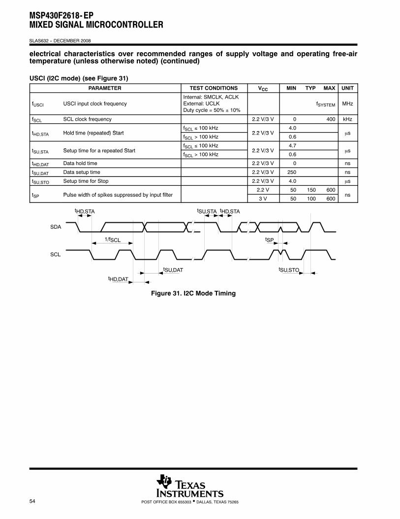
MSP430F2618-EPMIXED SIGNAL MICROCONTROLLER
SLAS632 -- DECEMBER 2008
54 POST OFFICE BOX 655303 DALLAS, TEXAS 75265
electrical characteristics over recommended ranges of supply voltage and operating free-airtemperature (unless otherwise noted) (continued)
USCI (I2C mode) (see Figure 31)PARAMETER TEST CONDITIONS VCC MIN TYP MAX UNIT
fUSCI USCI input clock frequencyInternal: SMCLK, ACLKExternal: UCLKDuty cycle = 50% 10%
fSYSTEM MHz
fSCL SCL clock frequency 2.2 V/3 V 0 400 kHz
t Hold time (repeated) StartfSCL 100 kHz
2 2 V/3 V4.0
stHD,STA Hold time (repeated) StartfSCL > 100 kHz
2.2 V/3 V0.6
s
t Setup time for a repeated StartfSCL 100 kHz
2 2 V/3 V4.7
stSU,STA Setup time for a repeated StartfSCL > 100 kHz
2.2 V/3 V0.6
s
tHD,DAT Data hold time 2.2 V/3 V 0 ns
tSU,DAT Data setup time 2.2 V/3 V 250 ns
tSU,STO Setup time for Stop 2.2 V/3 V 4.0 s
t Pulse width of spikes suppressed by input filter2.2 V 50 150 600
nstSP Pulse width of spikes suppressed by input filter3 V 50 100 600
ns
SDA
SCL
1/fSCL
tHD,DAT
tSU,DAT
tHD,STA tSU,STA tHD,STA
tSU,STO
tSP
Figure 31. I2C Mode Timing

MSP430F2618-EPMIXED SIGNAL MICROCONTROLLER
SLAS632 -- DECEMBER 2008
55POST OFFICE BOX 655303 DALLAS, TEXAS 75265
electrical characteristics over recommended ranges of supply voltage and operating free-airtemperature (unless otherwise noted) (continued)
Comparator_A+ (see Note 1)PARAMETER TEST CONDITIONS VCC MIN TYP MAX UNIT
I CAON 1 CARSEL 0 CAREF 02.2 V 25 40
AI(DD) CAON = 1, CARSEL = 0, CAREF = 03 V 45 60
A
ICAON = 1, CARSEL = 0,CAREF 1/2/3 no load at P2 3/CA0/TA1
2.2 V 30 50AI(Refladder/Refdiode) CAREF = 1/2/3, no load at P2.3/CA0/TA1
and P2.4/CA1/TA2 3 V 45 71A
V(IC) Common-mode input voltage CAON =1 2.2 V/3 V 0 VCC--1 V
V(Ref025) Voltage at 0.25 VCC node
VCC
PCA0 = 1, CARSEL = 1, CAREF = 1,no load at P2.3/CA0/TA1 andP2.4/CA1/TA2
2.2 V/3 V 0.23 0.24 0.25
V(Ref050)Voltage at 0.5VCC node
VCC
PCA0 = 1, CARSEL = 1, CAREF = 2,no load at P2.3/CA0/TA1 andP2.4/CA1/TA2
2.2 V/3 V 0.47 0.48 0.5
V See Figure 35 and Figure 36PCA0 = 1, CARSEL = 1, CAREF = 3,no load at P2 3/CA0/TA1 and
2.2 V 390 480 540mVV(RefVT) See Figure 35 and Figure 36 no load at P2.3/CA0/TA1 and
P2.4/CA1/TA2, TA = 85C 3 V 400 490 550mV
V(offset) Offset voltage See Note 2 2.2 V/3 V --30 30 mV
Vhys Input hysteresis CAON=1 2.2 V/3 V 0 0.7 1.4 mV
TA = 25C, Overdrive 10 mV, 2.2 V 80 165 300ns
t Response time, low-to-high and
TA = 25 C, Overdrive 10 mV,Without filter: CAF = 0 3 V 70 120 240
ns
t(response)Response time, low to high andhigh-to-low (see Note 3) TA = 25C, Overdrive 10 mV, 2.2 V 1.4 1.9 2.8
sTA = 25 C, Overdrive 10 mV,With filter: CAF = 1 3 V 0.9 1.5 2.2
s
NOTES: 1. The leakage current for the Comparator_A+ terminals is identical to Ilkg(Px.x) specification.2. The input offset voltage can be cancelled by using the CAEX bit to invert theComparator_A+ inputs on successivemeasurements.
The two successive measurements are then summed together.3. The response time is measured at P2.2/CAOUT/TA0/CA4 with an input voltage step, with Comparator_A+ already enabled
(CAON = 1). If CAON is set at the same time, a settling time of up to 300 ns is added to the response time.
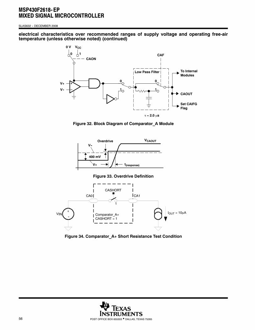
MSP430F2618-EPMIXED SIGNAL MICROCONTROLLER
SLAS632 -- DECEMBER 2008
56 POST OFFICE BOX 655303 DALLAS, TEXAS 75265
electrical characteristics over recommended ranges of supply voltage and operating free-airtemperature (unless otherwise noted) (continued)
_+
CAON
0
1
V+0
1
CAF
Low Pass Filter
2.0 s
To InternalModules
Set CAIFGFlag
CAOUTV--
VCC
1
0 V
0
Figure 32. Block Diagram of Comparator_A Module
Overdrive VCAOUT
t(response)V+
V--
400 mV
Figure 33. Overdrive Definition
CASHORT
1
Comparator_A+CASHORT = 1
CA1CA0
VIN+
--IOUT = 10A
Figure 34. Comparator_A+ Short Resistance Test Condition

MSP430F2618-EPMIXED SIGNAL MICROCONTROLLER
SLAS632 -- DECEMBER 2008
57POST OFFICE BOX 655303 DALLAS, TEXAS 75265
electrical characteristics over recommended ranges of supply voltage and operating free-airtemperature (unless otherwise noted) (continued)
typical characteristics -- Comparator A+
TA -- Free-Air Temperature -- C
400
450
500
550
600
650
--45 --25 --5 15 35 55 75 95
VCC = 3 V
Figure 35. V(RefVT) vs Temperature, VCC = 3 V
V (REFVT)--Reference
Volts--m
V
Typical
Figure 36. V(RefVT) vs Temperature, VCC = 2.2 V
TA -- Free-Air Temperature -- C
400
450
500
550
600
650
--45 --25 --5 15 35 55 75 95
VCC = 2.2 V
V (REFVT)--Reference
Volts--m
V
Typical
VIN/VCC -- Normalized Input Voltage -- V/V
1.00
10.00
100.00
0.0 0.2 0.4 0.6 0.8 1.0
Figure 37. Short Resistance vs VIN/VCC
VCC = 1.8V
VCC = 3.6V
VCC = 2.2V
VCC = 3.0V
ShortResistance
--k

MSP430F2618-EPMIXED SIGNAL MICROCONTROLLER
SLAS632 -- DECEMBER 2008
58 POST OFFICE BOX 655303 DALLAS, TEXAS 75265
electrical characteristics over recommended ranges of supply voltage and operating free-airtemperature (unless otherwise noted) (continued)
12-bit ADC power supply and input range conditions (see Note 1)PARAMETER TEST CONDITIONS VCC MIN TYP MAX UNIT
AVCC Analog supply voltageAVCC and DVCC are connected together,AVSS and DVSS are connected together,V(AVSS) = V(DVSS) = 0 V
2.2 3.6 V
V(P6.x/Ax)Analog input voltage(see Note 2)
All P6.0/A0 to P6.7/A7 terminals.Analog inputs selected in ADC12MCTLx registerand P6Sel.x = 1, 0 x 7,V(AVSS) VP6.x/Ax V(AVCC)
0 VAVCC V
IOperating supply currentinto AV terminal
fADC12CLK = 5 MHz, ADC12ON = 1, REFON = 0, 2.2 V 0.65 0.8mAIADC12 into AVCC terminal
(see Note 3)
fADC12CLK = 5 MHz, ADC12ON = 1, REFON = 0,SHT0 = 0, SHT1 = 0, ADC12DIV = 0 3 V 0.8 1.0
mA
IOperating supply currenti AV i l
fADC12CLK = 5 MHz, ADC12ON = 0,REFON = 1, REF2_5V = 1 3 V 0.5 0.7
AIREF+p g pp y
into AVCC terminal(see Note 4) fADC12CLK = 5 MHz, ADC12ON = 0, 2.2 V 0.5 0.7 mA(see Note 4) fADC12CLK = 5 MHz, ADC12ON = 0,
REFON = 1, REF2_5V = 0 3 V 0.5 0.7
CI † Input capacitanceOnly one terminal can be selected at one time,P6.x/Ax 2.2 V 40 pF
RI† Input MUX ON resistance 0 V VAx VAVCC 3 V 2000 † Limits verified by designNOTES: 1. The leakage current is defined in the leakage current table with P6.x/Ax parameter.
2. The analog input voltage range must be within the selected reference voltage range VR+ to VR-- for valid conversion results.3. The internal reference supply current is not included in current consumption parameter IADC12.4. The internal reference current is supplied via terminal AVCC. Consumption is independent of the ADC12ON control bit, unless a
conversion is active. The REFON bit enables to settle the built-in reference before starting an A/D conversion.
12-bit ADC external reference (see Note 1)PARAMETER TEST CONDITIONS VCC MIN MAX UNIT
VeREF+Positive externalreference voltage input VeREF+ > VREF--/VeREF-- (see Note 2) 1.4 VAVCC V
VREF-- /VeREF--Negative externalreference voltage input VeREF+ > VREF--/VeREF-- (see Note 3) 0 1.2 V
(VeREF+ -- VREF--/VeREF--)Differential externalreference voltage input VeREF+ > VREF--/VeREF-- (see Note 4) 1.4 VAVCC V
IVeREF+ Static input current 0V VeREF+ VAVCC 2.2 V/3 V 1 A
IVREF--/VeREF-- Static input current 0V VeREF-- VAVCC 2.2 V/3 V 1 A
NOTES: 1. The external reference is used during conversion to charge and discharge the capacitance array. The input capacitance, Ci, is alsothe dynamic load for an external reference during conversion. The dynamic impedance of the reference supply should follow therecommendations on analog-source impedance to allow the charge to settle for 12-bit accuracy.
2. The accuracy limits the minimum positive external reference voltage. Lower reference voltage levels may be applied with reducedaccuracy requirements.
3. Theaccuracy limits themaximumnegative external reference voltage. Higher reference voltage levelsmay beappliedwith reducedaccuracy requirements.
4. The accuracy limitsminimumexternal differential reference voltage. Lower differential reference voltage levelsmay be appliedwithreduced accuracy requirements.

MSP430F2618-EPMIXED SIGNAL MICROCONTROLLER
SLAS632 -- DECEMBER 2008
59POST OFFICE BOX 655303 DALLAS, TEXAS 75265
electrical characteristics over recommended ranges of supply voltage and operating free-airtemperature (unless otherwise noted) (continued)
12-bit ADC built-in referencePARAMETER TEST CONDITIONS VCC TA MIN TYP MAX UNIT
REF2_5V = 1 (2.5 V)3 V
--40C to 85C 2.4 2.5 2.6
VPositive built-inreference voltage
REF2_5V = 1 (2.5 V)IVREF+max IVREF+ IVREF+min
3 V105C 2.37 2.5 2.64
VVREF+ reference voltageoutput REF2_5V = 0 (1.5 V) 2.2 V/3 V --40C to 85C 1.44 1.5 1.56
Voutput REF2_5V = 0 (1.5 V)
IVREF+max IVREF+ IVREF+min2.2 V/3 V2.2 V/3 V 105C 1.42 1.5 1.57
AVCC minimum
REF2_5V = 0,IVREF+max IVREF+ IVREF+min
2.2
AVCC(min)
AVCC minimumvoltage, positivebuilt-in reference
REF2_5V = 1,--0.5mA IVREF+ IVREF+min
2.8 Vbuilt in referenceactive REF2_5V = 1,
--1mA IVREF+ IVREF+min2.9
ILoad current out of 2.2 V 0.01 --0.5
mAIVREF+Load current out ofVREF+ terminal 3 V 0.01 --1
mA
IVREF+ = 500 A +/-- 100 AAnalog input voltage 0 75 V
2.2 V 2
I †Load-currentregulation V
Analog input voltage ~0.75 V,REF2_5V = 0 3 V 2
LSBIL(VREF)+ † regulation, VREF+terminal IVREF+ = 500 A 100 A
Analog input voltage ~1.25 V,REF2_5V = 1
3 V 2
LSB
I ‡Load currentregulation V
IVREF+ = 100 A 900 A,C 5 F at 0 5 V 3 V 20 nsIDL(VREF) +‡ regulation VREF+
terminalCVREF+= 5 F, at ~0.5 VREF+,Error of conversion result 1 LSB
3 V 20 ns
CVREF+Capacitance at pinVREF+ (see Note 1)
REFON =1,0 mA IVREF+ IVREF+max
2.2 V/3 V 5 10 F
TREF+†Temperaturecoefficient ofbuilt-in reference
IVREF+ is a constant in the rangeof 0 mA IVREF+ 1 mA
2.2 V/3 V 100 ppm/C
tREFON†
Settle time ofinternal referencevoltage (seeFigure 38 and Note2)
IVREF+ = 0.5 mA, CVREF+ = 10 F,VREF+ = 1.5 V, VAVCC = 2.2 V
17 ms
† Limits characterized‡ Limits verified by designNOTES: 1. The internal buffer operational amplifier and the accuracy specifications require an external capacitor. All INL and DNL tests use
two capacitors between pins VREF+ and AVSS and VREF--/VeREF-- and AVSS: 10 F tantalum and 100 nF ceramic.2. The condition is that the error in a conversion started after tREFON is less than 0.5 LSB. The settling time depends on the external
capacitive load.
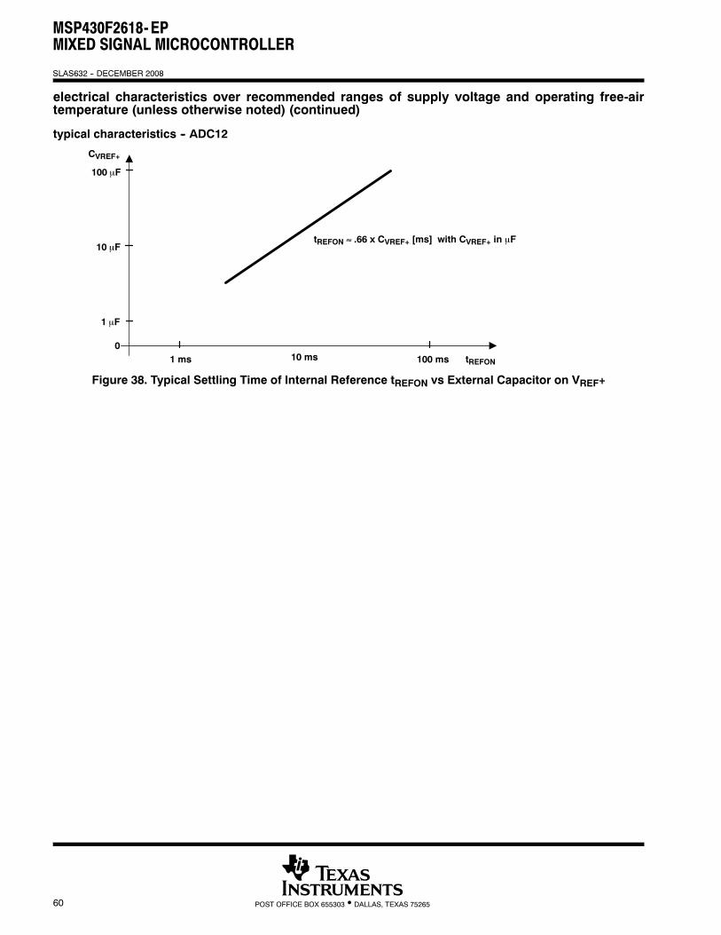
MSP430F2618-EPMIXED SIGNAL MICROCONTROLLER
SLAS632 -- DECEMBER 2008
60 POST OFFICE BOX 655303 DALLAS, TEXAS 75265
electrical characteristics over recommended ranges of supply voltage and operating free-airtemperature (unless otherwise noted) (continued)
typical characteristics -- ADC12
CVREF+
1 F
01 ms 10 ms 100 ms tREFON
tREFON .66 x CVREF+ [ms] with CVREF+ in F
100 F
10 F
Figure 38. Typical Settling Time of Internal Reference tREFON vs External Capacitor on VREF+

MSP430F2618-EPMIXED SIGNAL MICROCONTROLLER
SLAS632 -- DECEMBER 2008
61POST OFFICE BOX 655303 DALLAS, TEXAS 75265
electrical characteristics over recommended ranges of supply voltage and operating free-airtemperature (unless otherwise noted) (continued)
+--
10 F 100 nFAVSS
MSP430F261xMSP430F241x
+--
+--
10 F 100 nF
10 F 100 nF
AVCC
10 F 100 nFDVSS
DVCCFromPowerSupply
ApplyExternalReference
+--
Apply External Reference [VeREF+]or Use Internal Reference [VREF+] VREF+ or VeREF+
VREF--/VeREF--
Figure 39. Supply Voltage and Reference Voltage Design VREF--/VeREF-- External Supply
+--
10 F 100 nFAVSS
MSP430F261xMSP430F241x
+--
10 F 100 nF
AVCC
10 F 100 nFDVSS
DVCCFromPowerSupply
+--
Apply External Reference [VeREF+]or Use Internal Reference [VREF+] VREF+ or VeREF+
VREF--/VeREF--Reference Is InternallySwitched to AVSS
Figure 40. Supply Voltage and Reference Voltage Design VREF--/VeREF-- = AVSS, Internally Connected

MSP430F2618-EPMIXED SIGNAL MICROCONTROLLER
SLAS632 -- DECEMBER 2008
62 POST OFFICE BOX 655303 DALLAS, TEXAS 75265
electrical characteristics over recommended ranges of supply voltage and operating free-airtemperature (unless otherwise noted) (continued)
12-bit ADC timing parametersPARAMETER TEST CONDITIONS VCC MIN TYP MAX UNIT
fADC12CLKFor specified performance of ADC12linearity parameters 2.2V/3 V 0.45 5 6.3 MHz
fADC12OSC Internal ADC12 oscillatorADC12DIV = 0,fADC12CLK = fADC12OSC
2.2 V/ 3 V 3.7 5 6.3 MHz
t Conversion time
CVREF+ 5 F, Internal oscillator,fADC12OSC = 3.7 MHz to 6.3 MHz
2.2 V/ 3 V 2.06 3.51
stCONVERT Conversion timeExternal fADC12CLK from ACLK, MCLKor SMCLK, ADC12SSEL 0
13 ADC12DIV 1/fADC12CLK
s
tADC12ON‡Turn-on settling time ofthe ADC See Note 1 100 ns
t ‡ Sampling time RS = 400 , RI = 1000 , CI = 30 pF, 3 V 1220nstSample‡ Sampling time RS = 400 , RI = 1000 , CI = 30 pF,
= [RS + RI] x CI;(see Note 2) 2.2 V 1400ns
† Limits characterized‡ Limits verified by designNOTES: 1. Thecondition is that theerror ina conversionstarted after tADC12ON is less than0.5 LSB.The referenceand input signal arealready
settled.2. Approximately ten Tau () are needed to get an error of less than 0.5 LSB:
tSample = ln(2n+1) x (RS + RI) x CI+ 800 ns where n = ADC resolution = 12, RS = external source resistance.
12-bit ADC linearity parametersPARAMETER TEST CONDITIONS VCC MIN TYP MAX UNIT
E Integral linearity error1.4 V (VeREF+ -- VREF--/VeREF--) min 1.6 V
2 2 V/3 V2
LSBEI Integral linearity error1.6 V < (VeREF+ -- VREF--/VeREF--) min VAVCC
2.2 V/3 V1.7
LSB
ED Differential linearity error(VeREF+ -- VREF--/VeREF--)min (VeREF+ -- VREF--/VeREF--),CVREF+ = 10 F (tantalum) and 100 nF (ceramic)
2.2 V/3 V 1 LSB
EO Offset error(VeREF+ -- VREF--/VeREF--)min (VeREF+ -- VREF--/VeREF--),Internal impedance of source RS < 100 ,CVREF+ = 10 F (tantalum) and 100 nF (ceramic)
2.2 V/3 V 2 4 LSB
EG Gain error(VeREF+ -- VREF--/VeREF--)min (VeREF+ -- VREF--/VeREF--),CVREF+ = 10 F (tantalum) and 100 nF (ceramic)
2.2 V/3 V 1.1 2 LSB
ET Total unadjusted error(VeREF+ -- VREF--/VeREF--)min (VeREF+ -- VREF--/VeREF--),CVREF+ = 10 F (tantalum) and 100 nF (ceramic)
2.2 V/3 V 2 5 LSB
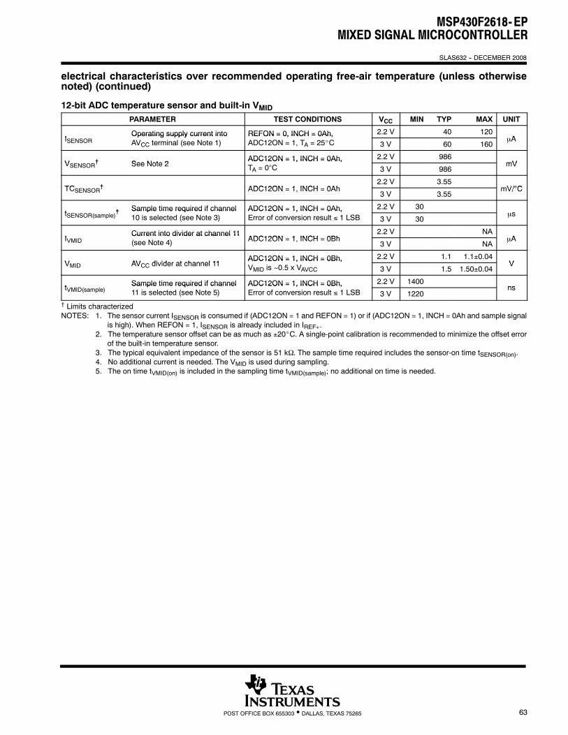
MSP430F2618-EPMIXED SIGNAL MICROCONTROLLER
SLAS632 -- DECEMBER 2008
63POST OFFICE BOX 655303 DALLAS, TEXAS 75265
electrical characteristics over recommended operating free-air temperature (unless otherwisenoted) (continued)
12-bit ADC temperature sensor and built-in VMIDPARAMETER TEST CONDITIONS VCC MIN TYP MAX UNIT
IOperating supply current into REFON = 0, INCH = 0Ah, 2.2 V 40 120
AISENSOROperating supply current intoAVCC terminal (see Note 1)
REFON = 0, INCH = 0Ah,ADC12ON = 1, TA = 25_C 3 V 60 160
A
V † See Note 2ADC12ON = 1, INCH = 0Ah, 2.2 V 986
mVVSENSOR† See Note 2ADC12ON = 1, INCH = 0Ah,TA = 0C 3 V 986
mV
TC † ADC12ON 1 INCH 0Ah2.2 V 3.55
mV/CTCSENSOR† ADC12ON = 1, INCH = 0Ah3 V 3.55
mV/C
t † Sample time required if channel ADC12ON = 1, INCH = 0Ah, 2.2 V 30stSENSOR(sample)†
Sample time required if channel10 is selected (see Note 3)
ADC12ON = 1, INCH = 0Ah,Error of conversion result 1 LSB 3 V 30
s
ICurrent into divider at channel 11
ADC12ON 1 INCH 0Bh2.2 V NA
AIVMIDCurrent into divider at channel 11(see Note 4) ADC12ON = 1, INCH = 0Bh
3 V NAA
V AV divider at channel 11ADC12ON = 1, INCH = 0Bh, 2.2 V 1.1 1.10.04
VVMID AVCC divider at channel 11ADC12ON = 1, INCH = 0Bh,VMID is ~0.5 x VAVCC 3 V 1.5 1.500.04
V
t Sample time required if channel ADC12ON = 1, INCH = 0Bh, 2.2 V 1400nstVMID(sample)
Sample time required if channel11 is selected (see Note 5)
ADC12ON = 1, INCH = 0Bh,Error of conversion result 1 LSB 3 V 1220
ns
† Limits characterizedNOTES: 1. The sensor current ISENSOR is consumed if (ADC12ON = 1 and REFON = 1) or if (ADC12ON = 1, INCH = 0Ah and sample signal
is high). When REFON = 1, ISENSOR is already included in IREF+.2. The temperature sensor offset can be as much as 20_C. A single-point calibration is recommended to minimize the offset error
of the built-in temperature sensor.3. The typical equivalent impedance of the sensor is 51 k. The sample time required includes the sensor-on time tSENSOR(on).4. No additional current is needed. The VMID is used during sampling.5. The on time tVMID(on) is included in the sampling time tVMID(sample); no additional on time is needed.

MSP430F2618-EPMIXED SIGNAL MICROCONTROLLER
SLAS632 -- DECEMBER 2008
64 POST OFFICE BOX 655303 DALLAS, TEXAS 75265
electrical characteristics over recommended ranges of supply voltage and operating free-airtemperature (unless otherwise noted) (continued)
12-bit DAC supply specificationsPARAMETER TEST CONDITIONS VCC TA MIN TYP MAX UNIT
AVCC Analog supply voltageAVCC = DVCC,AVSS = DVSS = 0 V
2.20 3.60 V
DAC12AMPx = 2, DAC12IR = 0,2 2V/3V
--40C to 85C 50 110DAC12AMPx 2, DAC12IR 0,DAC12_xDAT = 0x0800
2.2V/3V105C 69 150
Supply current,
DAC12AMPx = 2, DAC12IR = 1,DAC12_xDAT = x00800 ,
VeREF+ = VREF+ = AVCC
2.2V/3V 50 130
IDD
Supply current,single DAC channel(see Notes 1 and 2)
DAC12AMPx = 5, DAC12IR = 1,DAC12_xDAT = 0x0800,VeREF+ = VREF+ = AVCC
2.2V/3V 200 440
A
DAC12AMPx = 7, DAC12IR = 1,DAC12_xDAT = 0x0800,VeREF+ = VREF+ = AVCC
2.2V/3V 700 1500
PSRR
Power-supplyrejection ratio
DAC12_xDAT = 800h, VREF = 1.5 V,AVCC = 100mV
2.2V
70 dBPSRR rejection ratio(see Notes 3 and 4)
DAC12_xDAT = 800h, VREF = 1.5 V or 2.5 V,AVCC = 100mV
3V70 dB
NOTES: 1. No load at the output pin, DAC12_0 or DAC12_1, assuming that the control bits for the shared pins are set properly.2. Current into reference terminals not included. If DAC12IR = 1 current flows through the input divider; see Reference Input
specifications.3. PSRR = 20 logAVCC/VDAC12_xOUT}4. VREF is applied externally. The internal reference is not used.

MSP430F2618-EPMIXED SIGNAL MICROCONTROLLER
SLAS632 -- DECEMBER 2008
65POST OFFICE BOX 655303 DALLAS, TEXAS 75265
electrical characteristics over recommended operating free-air temperature (unless otherwisenoted) (continued)
12-bit DAC linearity specifications (see Figure 41)PARAMETER TEST CONDITIONS VCC MIN TYP MAX UNIT
Resolution 12-bit monotonic 12 bits
INL Integral nonlinearity (see Note 1)
VREF = 1.5 VDAC12AMPx = 7, DAC12IR = 1
2.2 V
2 0 8 0 LSBINL Integral nonlinearity (see Note 1)VREF = 2.5 VDAC12AMPx = 7, DAC12IR = 1
3 V2.0 8.0 LSB
DNLDifferential nonlinearity
VREF = 1.5 VDAC12AMPx = 7, DAC12IR = 1
2.2 V
0 4 1 0 LSBDNLDifferential nonlinearity(see Note 1) VREF = 2.5 V
DAC12AMPx = 7, DAC12IR = 13 V
0.4 1.0 LSB
Offset voltage without calibration
VREF = 1.5 VDAC12AMPx = 7, DAC12IR = 1
2.2 V
21
EO
Offset voltage without calibration(see Notes 1 and 2) VREF = 2.5 V
DAC12AMPx = 7, DAC12IR = 13 V
21
mVEO
Offset voltage with calibration
VREF = 1.5 VDAC12AMPx = 7, DAC12IR = 1
2.2 V
2 5
mV
Offset voltage with calibration(see Notes 1 and 2) VREF = 2.5 V
DAC12AMPx = 7, DAC12IR = 13 V
2.5
dE(O)/dTOffset error temperaturecoefficient (see Note 1) 2.2 V/3 V 30 V/C
E Gain error (see Note 1)VREF = 1.5 V 2.2 V
3 50 % FSREG Gain error (see Note 1)VREF = 2.5 V 3 V
3.50 % FSR
dE(G)/dTGain temperaturecoefficient (see Note 1) 2.2 V/3 V 10
ppm ofFSR/C
Ti f ff t lib tiDAC12AMPx = 2 100
tOffset CalTime for offset calibration(see Note 3)
DAC12AMPx = 3, 5 2.2 V/3 V 32 mstOffset_Cal (see Note 3)DAC12AMPx = 4, 6, 7
2.2 V/3 V
6
ms
NOTES: 1. Parameters calculated from the best-fit curve from 0x0A to 0xFFF. The best-fit curve method is used to deliver coefficients “a” and“b” of the first-order equation: y = a + b x. VDAC12_xOUT = EO + (1 + EG) (VeREF+/4095) DAC12_xDAT, DAC12IR = 1.
2. The offset calibration works on the output operational amplifier. Offset calibration is triggered setting bit DAC12CALON.3. The offset calibration can be done if DAC12AMPx = {2, 3, 4, 5, 6, 7}. The output operational amplifier is switched off with
DAC12AMPx={0,1}.TheDAC12moduleshouldbeconfiguredprior to initiatingcalibration.Port activityduringcalibrationmayaffectaccuracy and is not recommended.
Positive
Negative
VR+
Gain ErrorOffset Error
DAC Code
DAC VOUT
Ideal transferfunction
RLoad =
AVCC
CLoad = 100pF
2
DAC Output
Figure 41. Linearity Test Load Conditions and Gain/Offset Definition

MSP430F2618-EPMIXED SIGNAL MICROCONTROLLER
SLAS632 -- DECEMBER 2008
66 POST OFFICE BOX 655303 DALLAS, TEXAS 75265
electrical characteristics over recommended operating free-air temperature (unless otherwisenoted) (continued)
typical characteristics -- 12-bit DAC, linearity specifications
DAC12_xDAT -- Digital Code
--4
--3
--2
--1
0
1
2
3
4
0 512 1024 1536 2048 2560 3072 3584
VCC = 2.2 V, VREF = 1.5VDAC12AMPx = 7DAC12IR = 1
TYPICAL INL ERRORvs
DIGITAL INPUT DATA
4095
INL--IntegralN
onlinearityError--LSB
DAC12_xDAT -- Digital Code
--2.0
--1.5
--1.0
--0.5
0.0
0.5
1.0
1.5
2.0
0 512 1024 1536 2048 2560 3072 3584
VCC = 2.2 V, VREF = 1.5VDAC12AMPx = 7DAC12IR = 1
TYPICAL DNL ERRORvs
DIGITAL INPUT DATA
4095
DNL--DifferentialNonlinearityError--LSB

MSP430F2618-EPMIXED SIGNAL MICROCONTROLLER
SLAS632 -- DECEMBER 2008
67POST OFFICE BOX 655303 DALLAS, TEXAS 75265
electrical characteristics over recommended operating free-air temperature (unless otherwisenoted) (continued)
12-bit DAC output specificationsPARAMETER TEST CONDITIONS VCC MIN TYP MAX UNIT
No Load, VeREF+ = AVCC,DAC12_xDAT = 0h, DAC12IR = 1,DAC12AMPx = 7
0 0.005
VOutput voltage range
No Load, VeREF+ = AVCC,DAC12_xDAT = 0FFFh,DAC12IR = 1, DAC12AMPx = 7
2 2 V/3 V
AVCC--0.05 AVCC
VVOOutput voltage range(see Note 1 and Figure 44) RLoad= 3 k, VeREF+ = AVCC,
DAC12_xDAT = 0h, DAC12IR = 1,DAC12AMPx = 7
2.2 V/3 V
0 0.1
V
RLoad= 3 k, VeREF+ = AVCC,DAC12_xDAT = 0FFFh, DAC12IR =1, DAC12AMPx = 7
AVCC--0.13 AVCC
CL(DAC12)Max DAC12 loadcapacitance 2.2 V/3 V 100 pF
I Max DAC12 load current2.2V --0.5 +0.5
mAIL(DAC12) Max DAC12 load current3V --1.0 +1.0
mA
RLoad= 3 k, VO/P(DAC12) = 0 V,DAC12AMPx = 7, DAC12_xDAT = 0h 150 250
RO/P(DAC12)Output resistance(see Figure 44)
RLoad= 3 k, VO/P(DAC12) = AVCC,DAC12AMPx = 7,DAC12_xDAT = 0FFFh 2.2 V/3 V
150 250
(see Figure 44)
RLoad= 3 k,0.3 V < VO/P(DAC12) < AVCC -- 0.3 V,DAC12AMPx = 7
1 4
NOTE 1: Data is valid after the offset calibration of the output amplifier.
RO/P(DAC12_x)Max
0.3
AVCC
AVCC--0.3V VOUT
Min
RLoad
AVCC
CLoad= 100pF
2
ILoad
DAC12
O/P(DAC12_x)
Figure 44. DAC12_x Output Resistance Tests

MSP430F2618-EPMIXED SIGNAL MICROCONTROLLER
SLAS632 -- DECEMBER 2008
68 POST OFFICE BOX 655303 DALLAS, TEXAS 75265
electrical characteristics over recommended operating free-air temperature (unless otherwisenoted) (continued)
12-bit DAC reference input specificationsPARAMETER TEST CONDITIONS VCC MIN TYP MAX UNIT
VeReference input voltage DAC12IR = 0, (see Notes 1 and 2)
2 2 V/3 VAVCC/3 AVCC+0.2
VVeREF+Reference input voltagerange DAC12IR = 1, (see Notes 3 and 4)
2.2 V/3 VAVcc AVcc+0.2
V
DAC12_0 IR = DAC12_1 IR = 0 20 M
DAC12_0 IR = 1, DAC12_1 IR = 040 48 56Ri(VREF+),
RiReference input
iDAC12_0 IR = 0, DAC12_1 IR = 1 2.2 V/3 V
40 48 56(VREF+)
Ri(VeREF+)p
resistance DAC12_0 IR = DAC12_1 IR = 1DAC12_0 SREFx = DAC12_1 SREFx(see Note 5)
2.2 V/3 V
20 24 28
k
NOTES: 1. For a full-scale output, the reference input voltage can be as high as 1/3 of the maximum output voltage swing (AVCC).2. The maximum voltage applied at reference input voltage terminal VeREF+ = [AVCC -- VE(O)] / [3*(1 + EG)].3. For a full-scale output, the reference input voltage can be as high as the maximum output voltage swing (AVCC).4. The maximum voltage applied at reference input voltage terminal VeREF+ = [AVCC -- VE(O)] / (1 + EG).5. WhenDAC12IR = 1 andDAC12SREFx = 0 or 1 for both channels, the reference input resistive dividers for each DACare in parallel
reducing the reference input resistance.
12-bit DAC dynamic specifications, Vref = VCC, DAC12IR = 1 (see Figure 45 and Figure 46)PARAMETER TEST CONDITIONS VCC MIN TYP MAX UNIT
DAC12_xDAT = 800h, DAC12AMPx = 0 {2, 3, 4} 60 120
tON DAC12 on-time
_ ,ErrorV(O) < 0.5 LSB(see Note 1 and
DAC12AMPx = 0 {5, 6} 2.2 V/3 V 15 30 sON (see Note 1 andFigure 45) DAC12AMPx = 0 7
/
6 12
S ttli ti DAC12 DATDAC12AMPx = 2 100 200
tS(FS)Settling time,full scale
DAC12_xDAT =80h F7Fh 80h
DAC12AMPx = 3, 5 2.2 V/3 V 40 80 stS(FS) full scale 80h F7Fh 80hDAC12AMPx = 4, 6, 7
2.2 V/3 V
15 30
s
S ttli ti DAC12 xDAT = DAC12AMPx = 2 5
tS(C-C)Settling time,code to code
DAC12_xDAT =3F8h 408h 3F8h DAC12AMPx = 3, 5 2.2 V/3 V 2 stS(C-C) code to code 3F8h 408h 3F8hBF8h C08h BF8h DAC12AMPx = 4, 6, 7
2.2 V/3 V
1
s
DAC12 DATDAC12AMPx = 2 0.05 0.12
SR Slew rateDAC12_xDAT =80h F7Fh 80h
DAC12AMPx = 3, 5 2.2 V/3 V 0.35 0.7 V/sSR Slew rate 80h F7Fh 80hDAC12AMPx = 4, 6, 7
2.2 V/3 V
1.5 2.7
V/s
Glit h DAC12 DATDAC12AMPx = 2 600
Glitch energy,full scale
DAC12_xDAT =80h F7Fh 80h
DAC12AMPx = 3, 5 2.2 V/3 V 150 nV-sfull scale 80h F7Fh 80hDAC12AMPx = 4, 6, 7
2.2 V/3 V
30
nV s
NOTES: 1. RLoad and CLoad are connected to AVSS (not AVCC/2) in Figure 45.2. Slew rate applies to output voltage steps 200 mV.
RLoad
AVCC
CLoad = 100pF
2
DAC Output
RO/P(DAC12.x)
ILoad
Conversion 1 Conversion 2
VOUT
Conversion 3
GlitchEnergy
+/-- 1/2 LSB
+/-- 1/2 LSB
tsettleLH tsettleHL
= 3 k
Figure 45. Settling Time and Glitch Energy Testing

MSP430F2618-EPMIXED SIGNAL MICROCONTROLLER
SLAS632 -- DECEMBER 2008
69POST OFFICE BOX 655303 DALLAS, TEXAS 75265
electrical characteristics over recommended ranges of supply voltage and operating free-airtemperature (unless otherwise noted) (continued)
Conversion 1 Conversion 2
VOUT
Conversion 3
10%
tSRLH tSRHL
90%
10%
90%
Figure 46. Slew Rate Testing
12-bit DAC, dynamic specifications (continued) (TA = 25C, unless otherwise noted)PARAMETER TEST CONDITIONS VCC MIN TYP MAX UNIT
DAC12AMPx = {2, 3, 4}, DAC12SREFx = 2,DAC12IR = 1, DAC12_xDAT = 800h 40
BW--3dB
3-dB bandwidth,VDC = 1.5 V, VAC = 0.1 VPP(see Figure 47)
DAC12AMPx = {5, 6}, DAC12SREFx = 2,DAC12IR = 1, DAC12_xDAT = 800h 2.2 V/3 V 180 kHz
(see Figure 47)DAC12AMPx = 7, DAC12SREFx = 2,DAC12IR = 1, DAC12_xDAT = 800h 550
Channel-to-channel crosstalk
DAC12_0DAT = 800h, No load,DAC12_1DAT = 80h<-->F7Fh, RLoad = 3 k,fDAC12_1OUT = 10 kHz, Duty cycle = 50%
2 2 V/3 V
--80
dBChannel to channel crosstalk(see Note 1 and Figure 48) DAC12_0DAT = 80h<-->F7Fh, RLoad = 3 k,
DAC12_1DAT = 800h, No load,fDAC12_0OUT = 10 kHz, Duty cycle = 50%
2.2 V/3 V
--80
dB
NOTE 1: RLOAD = 3 k, CLOAD = 100 pF
VeREF+
AC
DC
RLoad
AVCC
CLoad= 100pF
2
ILoad
DAC12_xDACx
= 3 k
Figure 47. Test Conditions for 3-dB Bandwidth Specification
DAC12_xDAT 080h
VOUT
fToggle
7F7h
VDAC12_yOUT
080h 7F7h 080h
VDAC12_xOUTe
REF+ RLoad
AVCC
CLoad= 100pF
2
ILoadDAC12_1
RLoad
AVCC
CLoad= 100pF
2
ILoad
DAC12_0DAC0
DAC1
V
Figure 48. Crosstalk Test Conditions

MSP430F2618-EPMIXED SIGNAL MICROCONTROLLER
SLAS632 -- DECEMBER 2008
70 POST OFFICE BOX 655303 DALLAS, TEXAS 75265
electrical characteristics over recommended ranges of supply voltage and operating free-airtemperature (unless otherwise noted) (continued)
flash memory
PARAMETERTEST
CONDITIONS VCC MIN TYP MAX UNIT
VCC(PGM/ERASE) Program and erase supply voltage 2.2 3.6 V
fFTG Flash Timing Generator frequency 257 476 kHz
IPGM Supply current from DVCC during program 2.2 V/ 3.6 V 3 5 mA
IERASE Supply current from DVCC during erase 2.2 V/ 3.6 V 3 7 mA
tCPT Cumulative program time See Note 1 2.2 V/ 3.6 V 10 ms
tCMErase Cumulative mass erase time See Note 2 2.2 V/ 3.6 V 200 ms
Program/Erase endurance 104 105 cycles
tRetention Data retention duration TJ = 25C 100 years
tWord Word or byte program time See Note 3 35 tFTGtBlock, 0 Block program time for first byte or word See Note 3 30 tFTGtBlock, 1-63 Block program time for each additional byte or word See Note 3 21 tFTGtBlock, End Block program end-sequence wait time See Note 3 6 tFTGtMass Erase Mass erase time (see Note 4) See Note 3 10593 tFTGtSeg Erase Segment erase time See Note 3 4819 tFTGNOTES: 1. Thecumulativeprogram timemust not beexceededwhenwriting toa64-byte flashblock. This parameter applies to all programming
methods: individual word/byte write and block write modes.2. The mass erase duration generated by the flash timing generator is at least 11.1 ms ( = 5297x1/fFTG,max = 5297 1/476 kHz). To
achieve the required cumulativemass erase time, theFlashController’smass eraseoperation canbe repeateduntil this time ismet.A worst-case minimum of 19 cycles is required.
3. These values are hardwired into the Flash Controller’s state machine (tFTG = 1/fFTG).4. To erase the complete code area, the mass erase must be performed once with a dummy address in the range of the lower 64-kB
flash addresses and once with the dummy address in the upper 64-kB flash addresses.
RAMPARAMETER TEST CONDITIONS MIN MAX UNIT
VRAMh See Note 1 CPU halted 1.6 V
NOTE 1: This parameter defines theminimumsupply voltagewhen thedata in programmemoryRAMremain unchanged.Noprogramexecutionshould take place during this supply voltage condition.

MSP430F2618-EPMIXED SIGNAL MICROCONTROLLER
SLAS632 -- DECEMBER 2008
71POST OFFICE BOX 655303 DALLAS, TEXAS 75265
electrical characteristics over recommended operating free-air temperature (unless otherwisenoted) (continued)
JTAG interface
PARAMETERTEST
CONDITIONS VCC MIN TYP MAX UNIT
f TCK input frequency See Note 12.2 V 0 5
MHzfTCK TCK input frequency See Note 13 V 0 10
MHz
RInternal Internal pullup resistance on TMS, TCK, TDI/TCLK See Note 2 2.2 V/ 3 V 25 60 90 k
NOTES: 1. fTCK may be restricted to meet the timing requirements of the module selected.2. TMS, TDI/TCLK, and TCK pullup resistors are implemented in all versions.
JTAG fuse (see Note 1)PARAMETER TEST CONDITIONS MIN MAX UNIT
VCC(FB) Supply voltage during fuse-blow condition TA = 25C 2.5 V
VFB Voltage level on TDI/TCLK for fuse blow (F versions) 6 7 V
IFB Supply current into TDI/TCLK during fuse blow 100 mA
tFB Time to blow fuse 1 ms
NOTE 1: Once the fuse is blown, no further access to the MSP430 JTAG/Test and emulation features is possible. The JTAG block is switchedto bypass mode.

MSP430F2618-EPMIXED SIGNAL MICROCONTROLLER
SLAS632 -- DECEMBER 2008
72 POST OFFICE BOX 655303 DALLAS, TEXAS 75265
APPLICATION INFORMATIONPort P1 pin schematic: P1.0 to P1.7, input/output with Schmitt trigger
Direction0: Input1: Output
P1SEL.x
P1DIR.x
P1IN.x
P1IRQ.x
D
EN
Module X IN
Module X OUT
P1OUT.x
Interrupt Edge Select
Q
EN
Set
P1SEL.x
P1IES.x
P1IFG.x
P1IE.x
P1.0/TACLK/CAOUTP1.1/TA0P1.2/TA1P1.3/TA2P1.4/SMCLKP1.5/TA0P1.6/TA1P1.7/TA2
DVSS
DVCC
Pad Logic
1
1
0
1
0
1
0
P1REN.x

MSP430F2618-EPMIXED SIGNAL MICROCONTROLLER
SLAS632 -- DECEMBER 2008
73POST OFFICE BOX 655303 DALLAS, TEXAS 75265
Port P1 (P1.0 to P1.7) pin functions
PIN NAME (P1 X) X FUNCTIONCONTROL BITS / SIGNALS
PIN NAME (P1.X) X FUNCTIONP1DIR.x P1SEL.x
P1.0/TACLK 0 P1.0 (I/O) I: 0; O: 1 0/
Timer_A3.TACLK 0 1
CAOUT 1 1
P1.1/TA0 1 P1.1 (I/O) I: 0; O: 1 0/
Timer_A3.CCI0A 0 1
Timer_A3.TA0 1 1
P1.2/TA1 2 P1.2 (I/O) I: 0; O: 1 0/
Timer_A3.CCI0A 0 1
Timer_A3.TA0 1 1
P1.3/TA2 3 P1.3 (I/O) I: 0; O: 1 0/
Timer_A3.CCI0A 0 1
Timer_A3.TA0 1 1
P1.4/SMCLK 4 P1.4 (I/O) I: 0; O: 1 0/
SMCLK 1 1
P1.5/TA0 5 P1.5 (I/O) I: 0; O: 1 0/
Timer_A3.CCI0A 0 1
Timer_A3.TA0 1 1
P1.6/TA1 6 P1.6 (I/O) I: 0; O: 1 0/
Timer_A3.CCI0A 0 1
Timer_A3.TA1 1 1
P1.7/TA2 7 P1.7 (I/O) I: 0; O: 1 0/
Timer_A3.CCI0A 0 1
Timer_A3.TA2 1 1

MSP430F2618-EPMIXED SIGNAL MICROCONTROLLER
SLAS632 -- DECEMBER 2008
74 POST OFFICE BOX 655303 DALLAS, TEXAS 75265
Port P2 pin schematic: P2.0 to P2.4, P2.6, and P2.7, input/output with Schmitt trigger
P2.0/ACLK/CA2P2.1/TAINCLK/CA3P2.2/CAOUT/TA0/CA4P2.3/CA0/TA1P2.4/CA1/TA2P2.6/ADC12CLK/DMAE0/CA6P2.7/TA0/CA7
Direction0: Input1: Output
P2SEL.x
P2DIR.x
P2IN.x
P2IRQ.x
D
EN
Module X IN
Module X OUT
P2OUT.x
Interrupt Edge Select
Q
EN
Set
P2SEL.x
P2IES.x
P2IFG.x
P2IE.x
DVSS
DVCC
P2REN.x
Pad Logic
1
1
0
1
0
1
0
Bus Keeper
EN
CAPD.x
FromComparator_A
ToComparator_A

MSP430F2618-EPMIXED SIGNAL MICROCONTROLLER
SLAS632 -- DECEMBER 2008
75POST OFFICE BOX 655303 DALLAS, TEXAS 75265
Port P2.0, P2.3, P2.4, P2.6 and P2.7 pin functions
PIN NAME (P2 X) X FUNCTIONCONTROL BITS / SIGNALS
PIN NAME (P2.X) X FUNCTIONCAPD.x P2DIR.x P2SEL.x
P2.0/ACLK/CA2 0 P2.0 (I/O) 0 I: 0; O: 1 0/ /
ACLK 0 1 1
CA2 1 X X
P2.1/TAINCLK/CA3 1 P2.1 (I/O) 0 I: 0; O: 1 0/ /
Timer_A3.INCLK 0 0 1
DVSS 0 1 1
CA3 1 X X
P2.2/CAOUT/TA0/ 2 P2.2 (I/O) 0 I: 0; O: 1 0/ / /CA4 CAOUT 0 1 1
TA0 0 0 1
CA4 1 X X
P2.3/CA0/TA1 3 P2.3 (I/O) 0 I: 0; O: 1 0/ /
Timer_A3.TA1 0 1 1
CA0 1 X X
P2.4/CA1/TA2 4 P2.4 (I/O) 0 I: 0; O: 1 0/ /
Timer_A3.TA2 0 1 X
CA1 1 X 1
P2.6/ADC12CLK/ 6 P2.6 (I/O) 0 I: 0; O: 1 0/ /DMAE0/CA6 ADC12CLK 0 1 1
DMAE0 0 0 1
CA6 1 X X
P2.7/TA0/CA7 7 P2.7 (I/O) 0 I: 0; O: 1 0/ /
Timer_A3.TA0 0 1 1
CA7 1 X X
NOTE: X: Don’t care.

MSP430F2618-EPMIXED SIGNAL MICROCONTROLLER
SLAS632 -- DECEMBER 2008
76 POST OFFICE BOX 655303 DALLAS, TEXAS 75265
Port P2 pin schematic: P2.5, input/output with Schmitt trigger
Direction0: Input1: Output
P2SEL.x
P2DIR.5
P2IN.5
P2IRQ.5
D
EN
Module X IN
Module X OUT
P2OUT.5
Interrupt Edge Select
Q
EN
Set
P2SEL.5
P2IES.5
P2IFG.5
P2IE.5
P2.5/ROSC/CA5
DVSS
DVCC 1
1
0
1
0
1
0
Bus Keeper
EN
DCOR
To DCO
Pad Logic
From Comparator
To Comparator
CAPD.5
in DCO
P2REN.5
Port P2.5 pin functions
PIN NAME (P2 X) X FUNCTIONCONTROL BITS / SIGNALS
PIN NAME (P2.X) X FUNCTIONCAPD DCOR P2DIR.5 P2SEL.5
P2.5/ROSC/CA5 5 P2.5 (I/O) 0 0 I: 0; O: 1 0/ OSC/
ROSC (see Note 2) 0 1 X X
DVSS 0 0 1 1
CA5 1 or selected 0 X X
NOTES: 1. X: Don’t care.2. If Rosc is used it is connected to an external resistor.

MSP430F2618-EPMIXED SIGNAL MICROCONTROLLER
SLAS632 -- DECEMBER 2008
77POST OFFICE BOX 655303 DALLAS, TEXAS 75265
Port P3 pin schematic: P3.0 to P3.7, input/output with Schmitt trigger
Direction0: Input1: Output
P3SEL.x
P3DIR.x
P3IN.x
D
EN
Module X IN
Module X OUT
P3OUT.x
DVSS
DVCC
Pad Logic
1
1
0
1
0
1
0
P3.0/UCB0STE/UCA0CLKP3.1/UCB0SIMO/UCB0SDAP3.2/UCB0SOMI/UCB0SCLP3.3/UCB0CLK/UCA0STEP3.4/UCA0TXD/UCA0SIMOP3.5/UCA0RXD/UCA0SOMIP3.6/UCA1TXD/UCA1SIMOP3.7/UCA1RXD/UCA1SOMI
P3REN.x
Module direction
Port P3.0 to P3.7 pin functions
PIN NAME (P3 X) X FUNCTIONCONTROL BITS / SIGNALS
PIN NAME (P3.X) X FUNCTIONP3DIR.x P3SEL.x
P3.0/UCB0STE/ 0 P3.0 (I/O) I: 0; O: 1 0/ /UCA0CLK UCB0STE/UCA0CLK (see Note 2 and 4) X 1
P3.1/UCB0SIMO/ 1 P3.1 (I/O) I: 0; O: 1 0/ /UCB0SDA UCB0SIMO/UCB0SDA (see Note 2 and 3) X 1
P3.2/UCB0SOMI/ 2 P3.2 (I/O) I: 0; O: 1 0/ /UCB0SCL UCB0SOMI/UCB0SCL (see Note 2 and 3) X 1
P3.3/UCB0CLK/ 3 P3.3 (I/O) I: 0; O: 1 0/ /UCA0STE UCB0CLK/UCA0STE (see Note 2) X 1
P3.4/UCA0TXD/ 4 P3.4 (I/O) I: 0; O: 1 0/ /UCA0SIMO UCA0TXD/UCA0SIMO (see Note 2) X 1
P3.5/UCA0RXD/ 5 P3.5 (I/O) I: 0; O: 1 0/ /UCA0SOMI UCA0RXD/UCA0SOMI (see Note 2) X 1
P3.6/UCA1TXD/ 6 P3.6 (I/O) I: 0; O: 1 0/ /UCA1SIMO UCA1TXD/UCA1SIMO (see Note 2) X 1
P3.7/UCA1RXD/ 7 P3.7 (I/O) I: 0; O: 1 0/ /UCA1SOMI UCA1RXD/UCA1SOMI (see Note 2) X 1
NOTES: 1. X: Don’t care.2. The pin direction is controlled by the USCI module.3. In case the I2C functionality is selected the output drives only the logical 0 to VSS level.4. UCA0CLK function takes precedence over UCB0STE function. If the pin is required as UCA0CLK input or output, USCI A0/B0 is
forced to 3-wire SPI mode if 4-wire SPI mode is selected.

MSP430F2618-EPMIXED SIGNAL MICROCONTROLLER
SLAS632 -- DECEMBER 2008
78 POST OFFICE BOX 655303 DALLAS, TEXAS 75265
Port P4 pin schematic: P4.0 to P4.7, input/output with Schmitt trigger
P4.0/TB0P4.1/TB1P4.2/TB2P4.3/TB3P4.4/TB4P4.5/TB5P4.6/TB6P4.7/TBCLK
P4SEL.x
P4DIR.x
P4IN.x
Module X IN
Module X OUT
P4OUT.x
P4REN.x
Direction0: Input1: Output
D
EN
DVSS
DVCC
Pad Logic
1
1
0
1
0
1
0
Port P4.0 to P4.7 pin functions
PIN NAME (P4 X) X FUNCTIONCONTROL BITS / SIGNALS
PIN NAME (P4.X) X FUNCTIONP4DIR.x P4SEL.x
P4.0/TB0 0 P4.0 (I/O) I: 0; O: 1 0/
Timer_B7.CCI0A and Timer_B7.CCI0B 0 1
Timer_B7.TB0 1 1
P4.1/TB1 1 P4.1 (I/O) I: 0; O: 1 0/
Timer_B7.CCI1A and Timer_B7.CCI1B 0 1
Timer_B7.TB1 1 1
P4.2/TB2 2 P4.2 (I/O) I: 0; O: 1 0/
Timer_B7.CCI2A and Timer_B7.CCI2B 0 1
Timer_B7.TB2 1 1
P4.3/TB3 3 P4.3 (I/O) I: 0; O: 1 0/
Timer_B7.CCI3A and Timer_B7.CCI3B 0 1
Timer_B7.TB3 1 1
P4.4/TB4 4 P4.4 (I/O) I: 0; O: 1 0/
Timer_B7.CCI4A and Timer_B7.CCI4B 0 1
Timer_B7.TB4 1 1
P4.5/TB5 5 P4.5 (I/O) I: 0; O: 1 0/
Timer_B7.CCI5A and Timer_B7.CCI5B 0 1
Timer_B7.TB5 1 1
P4.6/TB6 6 P4.6 (I/O) I: 0; O: 1 0/
Timer_B7.CCI6A and Timer_B7.CCI6B 0 1
Timer_B7.TB6 1 1
P4.7/TBCLK 7 P4.7 (I/O) I: 0; O: 1 0/
Timer_B7.TBCLK 1 1

MSP430F2618-EPMIXED SIGNAL MICROCONTROLLER
SLAS632 -- DECEMBER 2008
79POST OFFICE BOX 655303 DALLAS, TEXAS 75265
Port P5 pin schematic: P5.0 to P5.7, input/output with Schmitt trigger
P5SEL.x
P5DIR.x
P5IN.x
Module X IN
Module X OUT
P5OUT.x
P5REN.x
P5.0/UCB1STE/UCA1CLKP5.1/UCB1SIMO/UCB1SDAP5.2/UCB1SOMI/UCB1SCLP5.3/UCB1CLK/UCA1STEP5.4/MCLKP5.5/SMCLKP5.6/ACLKP5.7/TBOUTH/SVSOUT
ModuleDirection
Direction0: Input1: Output
D
EN
DVSS
DVCC
Pad Logic
1
1
0
1
0
1
0
Port P5.0 to P5.7 pin functions
PIN NAME (P5 X) X FUNCTIONCONTROL BITS / SIGNALS
PIN NAME (P5.X) X FUNCTIONP5DIR.x P5SEL.x
P5.0/UCB1STE/ 0 P5.0 (I/O) I: 0; O: 1 0/ /UCA1CLK UCB1STE/UCA1CLK (see Note 2 and 4) X 1
P5.1/UCB1SIMO/ 1 P5.1 (I/O) I: 0; O: 1 0/ /UCB1SDA UCB1SIMO/UCB1SDA (see Note 2 and 3) X 1
P5.2/UCB1SOMI/ 2 P5.2 (I/O) I: 0; O: 1 0/ /UCB1SCL UCB1SOMI/UCB1SCL (see Note 2 and 3) X 1
P5.3/UCB1CLK/ 3 P5.3 (I/O) I: 0; O: 1 0/ /UCA1STE UCB1CLK/UCA1STE (see Note 2) X 1
P5.4/MCLK 4 P5.0 (I/O) I: 0; O: 1 0/
MCLK 1 1
P5.5/SMCLK 5 P5.1 (I/O) I: 0; O: 1 0/
SMCLK 1 1
P5.6/ACLK 6 P5.2 (I/O) I: 0; O: 1 0/
ACLK 1 1
P5.7/TBOUTH/ 7 P5.7 (I/O) I: 0; O: 1 0/ /SVSOUT TBOUTH 0 1
SVSOUT 1 1
NOTES: 1. X: Don’t care.2. The pin direction is controlled by the USCI module.3. In case the I2C functionality is selected the output drives only the logical 0 to VSS level.4. UCA1CLK function takes precedence over UCB1STE function. If the pin is required as UCA1CLK input or output USCI A1/B1 will
be forced to 3-wire SPI mode if 4-wire SPI mode is selected.

MSP430F2618-EPMIXED SIGNAL MICROCONTROLLER
SLAS632 -- DECEMBER 2008
80 POST OFFICE BOX 655303 DALLAS, TEXAS 75265
Port P6 pin schematic: P6.0 to P6.4, input/output with Schmitt trigger
Direction0: Input1: Output
P6SEL.x
P6DIR.x
P6IN.x
D
EN
Module X IN
Module X OUT
P6OUT.x
P6.0/A0P6.1/A1P6.2/A2P6.3/A3P6.4/A4
DVSS
DVCC
Pad Logic
1
1
0
1
0
1
0
Bus Keeper
EN
ADC12 Ax
P6REN.x
Port P6.0 to P6.4 pin functions
PIN NAME (P6 X) X FUNCTIONCONTROL BITS / SIGNALS
PIN NAME (P6.X) X FUNCTIONP6DIR.x P6SEL.x
P6.0/A0 0 P6.0 (I/O) I: 0; O: 1 0/
A0 (see Note 2) X X
P6.1/A1 1 P6.1 (I/O) I: 0; O: 1 0/
A1 (see Note 2) X X
P6.2/A2 2 P6.2 (I/O) I: 0; O: 1 0/
A2 (see Note 2) X X
P6.3/A3 3 P6.3 (I/O) I: 0; O: 1 0/
A3 (see Note 2) X X
P6.4/A4 4 P6.4 (I/O) I: 0; O: 1 0/
A4 (see Note 2) X X
NOTES: 1. X: Don’t care.2. The ADC12 channel Ax is connected to AVss internally if not selected.

MSP430F2618-EPMIXED SIGNAL MICROCONTROLLER
SLAS632 -- DECEMBER 2008
81POST OFFICE BOX 655303 DALLAS, TEXAS 75265
Port P6 pin schematic: P6.5 and P6.6, input/output with Schmitt trigger
P6.5/A5/DAC1P6.6/A6/DAC0
Direction0: Input1: Output
P6SEL.x
P6DIR.x
P6IN.x
D
EN
Module X IN
Module X OUT
P6OUT.x
DVSS
DVCC
P6REN.x
Pad Logic
1
1
0
1
0
1
0
Bus Keeper
EN
ADC12 Ax
DAC12AMP > 0
DAC12_0OUT
ADC12 Ax
Port P6.5 to P6.6 pin functionsCONTROL BITS / SIGNALS
PIN NAME (P6.X) X FUNCTIONP6DIR.x P6SEL.x
CAPD.x orDAC12AMP > 0
P6.5/A5/DAC1† 5 P6.5 (I/O) I: 0; O: 1 0 0/ / †
DVSS 1 1 0
A5 (see Note 2) X X 1
DAC1 (DA12OPS= 1, see Note 3) X X 1
P6.6/A6/DAC0† 6 P6.6 (I/O) I: 0; O: 1 0 0/ / †
DVSS 1 1 0
A6 (see Note 2) X X 1
DAC0 (DA12OPS= 0, see Note 3) X X 1† MSP430F261x devices onlyNOTES: 1. X: Don’t care.
2. The ADC12 channel Ax is connected to AVss internally if not selected.3. The DAC outputs are floating if not selected.
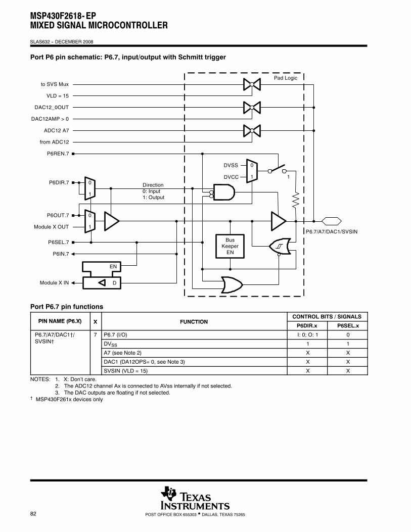
MSP430F2618-EPMIXED SIGNAL MICROCONTROLLER
SLAS632 -- DECEMBER 2008
82 POST OFFICE BOX 655303 DALLAS, TEXAS 75265
Port P6 pin schematic: P6.7, input/output with Schmitt trigger
Direction0: Input1: Output
P6SEL.7
P6DIR.7
P6IN.7
D
EN
Module X IN
Module X OUT
P6OUT.7
P6.7/A7/DAC1/SVSIN
DVSS
DVCC
P6REN.7
Pad Logic
1
1
0
1
0
1
0
Bus Keeper
EN
ADC12 A7
DAC12AMP > 0
DAC12_0OUT
VLD = 15
to SVS Mux
from ADC12
Port P6.7 pin functions
PIN NAME (P6 X) X FUNCTIONCONTROL BITS / SIGNALS
PIN NAME (P6.X) X FUNCTIONP6DIR.x P6SEL.x
P6.7/A7/DAC1†/ 7 P6.7 (I/O) I: 0; O: 1 0/ / †/SVSIN† DVSS 1 1
A7 (see Note 2) X X
DAC1 (DA12OPS= 0, see Note 3) X X
SVSIN (VLD = 15) X X
NOTES: 1. X: Don’t care.2. The ADC12 channel Ax is connected to AVss internally if not selected.3. The DAC outputs are floating if not selected.
† MSP430F261x devices only

MSP430F2618-EPMIXED SIGNAL MICROCONTROLLER
SLAS632 -- DECEMBER 2008
83POST OFFICE BOX 655303 DALLAS, TEXAS 75265
Port P7 pin schematic: P7.0 to P7.7, input/output with Schmitt trigger†
Direction0: Input1: Output
P7SEL.x
P7DIR.x
P7IN.x
D
EN
Module X IN
VSS
P7OUT.x
P7.x
DVSS
DVCC
P7REN.x Pad Logic
1
1
0
1
0
1
0
0
Port P7.0 to P7.7 pin functions†
PIN NAME (P7 X) X FUNCTIONCONTROL BITS / SIGNALS
PIN NAME (P7.X) X FUNCTIONP7DIR.x P7SEL.x
P7.0 0 P7.0 (I/O) I: 0; O: 1 0
Input X 1
P7.1 1 P7.1 (I/O) I: 0; O: 1 0
Input X 1
P7.2 2 P7.2 (I/O) I: 0; O: 1 0
Input X 1
P7.3 3 P7.3 (I/O) I: 0; O: 1 0
Input X 1
P7.4 4 P7.4 (I/O) I: 0; O: 1 0
Input X 1
P7.5 5 P7.5 (I/O) I: 0; O: 1 0
Input X 1
P7.6 6 P7.6 (I/O) I: 0; O: 1 0
Input X 1
P7.7 7 P7.7 (I/O) I: 0; O: 1 0
Input X 1† 80-pin devices only

MSP430F2618-EPMIXED SIGNAL MICROCONTROLLER
SLAS632 -- DECEMBER 2008
84 POST OFFICE BOX 655303 DALLAS, TEXAS 75265
Port P8 pin schematic: P8.0 to P8.5, input/output with Schmitt trigger†
Direction0: Input1: Output
P8SEL.x
P8DIR.x
P8IN.x
D
EN
Module X IN
VSS
P8OUT.x
P8.0P8.1P8.2P8.3P8.4P8.5
DVSS
DVCC
P8REN.x Pad Logic
1
1
0
1
0
1
0
0
Port P8.0 to P8.5 pin functions†
PIN NAME (P8 X) X FUNCTIONCONTROL BITS / SIGNALS
PIN NAME (P8.X) X FUNCTIONP8DIR.x P8SEL.x
P8.0 0 P8.0 (I/O) I: 0; O: 1 0
Input X 1
P8.1 1 P8.1 (I/O) I: 0; O: 1 0
Input X 1
P8.2 2 P8.2 (I/O) I: 0; O: 1 0
Input X 1
P8.3 3 P8.3 (I/O) I: 0; O: 1 0
Input X 1
P8.4 4 P8.4 (I/O) I: 0; O: 1 0
Input X 1
P8.5 5 P8.5 (I/O) I: 0; O: 1 0
Input X 1† 80-pin devices only

MSP430F2618-EPMIXED SIGNAL MICROCONTROLLER
SLAS632 -- DECEMBER 2008
85POST OFFICE BOX 655303 DALLAS, TEXAS 75265
Port P8 pin schematic: P8.6, input/output with Schmitt trigger†
Direction0: Input1: Output
P8SEL.6
P8DIR.6
P8IN.6
D
EN
Module X IN
Module X OUT
P8OUT.6
DVSS
DVCC
Pad Logic
1
1
0
1
0
1
0
Bus Keeper
EN
P8.6/XOUT
P8.7/XIN
P8SEL.7
P8REN.6
1
0XT2CLK
XT2 off
BCSCTL3.XT2Sx = 11
From P8.7/XIN
Port P8.6 pin functions†
PIN NAME (P8 X) X FUNCTIONCONTROL BITS / SIGNALS
PIN NAME (P8.X) X FUNCTIONP8DIR.x P8SEL.x
P8.6/XOUT 6 P8.6 (I/O) I: 0; O: 1 0/
XOUT (default) 0 1
DVSS 1 1† 80-pin devices only
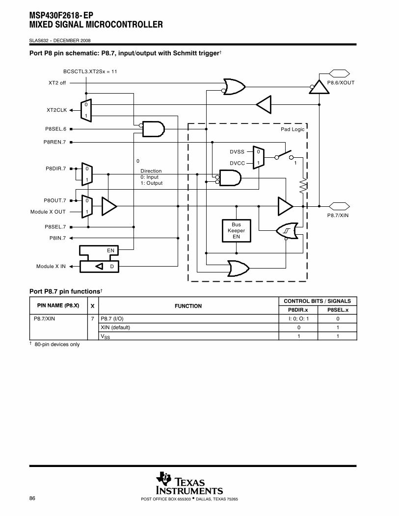
MSP430F2618-EPMIXED SIGNAL MICROCONTROLLER
SLAS632 -- DECEMBER 2008
86 POST OFFICE BOX 655303 DALLAS, TEXAS 75265
Port P8 pin schematic: P8.7, input/output with Schmitt trigger†
Direction0: Input1: Output
P8SEL.7
P8DIR.7
P8IN.7
D
EN
Module X IN
Module X OUT
P8OUT.7
DVSS
DVCC
Pad Logic
1
1
0
1
0
1
0
Bus Keeper
EN
P8SEL.6
P8.7/XIN
1
0XT2CLK
0
P8.6/XOUTXT2 off
BCSCTL3.XT2Sx = 11
P8REN.7
Port P8.7 pin functions†
PIN NAME (P8 X) X FUNCTIONCONTROL BITS / SIGNALS
PIN NAME (P8.X) X FUNCTIONP8DIR.x P8SEL.x
P8.7/XIN 7 P8.7 (I/O) I: 0; O: 1 0/
XIN (default) 0 1
VSS 1 1† 80-pin devices only

MSP430F2618-EPMIXED SIGNAL MICROCONTROLLER
SLAS632 -- DECEMBER 2008
87POST OFFICE BOX 655303 DALLAS, TEXAS 75265
APPLICATION INFORMATION
JTAG pins: TMS, TCK, TDI/TCLK, TDO/TDI, input/output with Schmitt trigger
TDI
TDO
TMS
TCK
Test
JTAG
and
EmulationModule
Burn and TestFuse
Controlled by JTAG
Controlled by JTAG
Controlledby JTAG
DVCC
DVCC
DVCC During Programming Activity andDuring Blowing of the Fuse, PinTDO/TDI Is Used to Apply the TestInput Data for JTAG Circuitry
TDO/TDI
TDI/TCLK
TMS
TCK
Fuse
DVCC

MSP430F2618-EPMIXED SIGNAL MICROCONTROLLER
SLAS632 -- DECEMBER 2008
88 POST OFFICE BOX 655303 DALLAS, TEXAS 75265
APPLICATION INFORMATIONJTAG fuse check mode
MSP430 devices that have the fuse on the TDI/TCLK terminal have a fuse check mode that tests the continuityof the fuse the first time the JTAG port is accessed after a power-on reset (POR). When activated, a fuse checkcurrent, ITF, of 1 mA at 3 V or 2.5 mA at 5 V can flow from the TDI/TCLK pin to ground if the fuse is not burned.Care must be taken to avoid accidentally activating the fuse check mode and increasing overall system powerconsumption.Activation of the fuse check mode occurs with the first negative edge on the TMS pin after power up or if theTMS is being held low during power up. The second positive edge on the TMS pin deactivates the fuse checkmode. After deactivation, the fuse check mode remains inactive until another POR occurs. After each POR thefuse check mode has the potential to be activated.The fuse check current flows only when the fuse check mode is active and the TMS pin is in a low state (seeFigure 49). Therefore, the additional current flow can be prevented by holding the TMS pin high (defaultcondition).
Time TMS Goes Low After POR
TMS
ITFITDI/TCLK
Figure 49. Fuse Check Mode Current

MSP430F2618-EPMIXED SIGNAL MICROCONTROLLER
SLAS632 -- DECEMBER 2008
89POST OFFICE BOX 655303 DALLAS, TEXAS 75265
Data Sheet Revision HistoryLITERATURENUMBER SUMMARY
SLAS541 Product Preview release
SLAS541A
Production Data releaseCorrected the format and the content shown on the first page.Corrected pin number of P3.6 and P3.7 in 64-pin package in the terminal function list.Corrected the port schematics.Corrected “calibration data” section (page 20). Typos and formatting corrected.Added the figure “typical characteristics -- LPM4 current” (Page 33).
SLAS541B Added preview of MSP430F261x BGA devices.SLAS541C Release to market of MSP430F261x BGA devices
SLAS541D
Added the ESD disclaimer (page 1).Added reserved BGA pins to the terminal function list (pages 10 and following).Corrected the references in the output port parameters (page 36).Corrected the cumulative program time of the flash (page 75).

PACKAGING INFORMATION
Orderable Device Status (1) PackageType
PackageDrawing
Pins PackageQty
Eco Plan (2) Lead/Ball Finish MSL Peak Temp (3)
MSP430F2618TGQWTEP ACTIVE BGA MI CROSTA
R JUNI OR
GQW 113 250 TBD SNPB Level-3-235C-168 HR
V62/09620-01XA ACTIVE BGA MI CROSTA
R JUNI OR
GQW 113 250 TBD SNPB Level-3-235C-168 HR
(1) The marketing status values are defined as follows:ACTIVE: Product device recommended for new designs.LIFEBUY: TI has announced that the device will be discontinued, and a lifetime-buy period is in effect.NRND: Not recommended for new designs. Device is in production to support existing customers, but TI does not recommend using this part ina new design.PREVIEW: Device has been announced but is not in production. Samples may or may not be available.OBSOLETE: TI has discontinued the production of the device.
(2) Eco Plan - The planned eco-friendly classification: Pb-Free (RoHS), Pb-Free (RoHS Exempt), or Green (RoHS & no Sb/Br) - please checkhttp://www.ti.com/productcontent for the latest availability information and additional product content details.TBD: The Pb-Free/Green conversion plan has not been defined.Pb-Free (RoHS): TI's terms "Lead-Free" or "Pb-Free" mean semiconductor products that are compatible with the current RoHS requirementsfor all 6 substances, including the requirement that lead not exceed 0.1% by weight in homogeneous materials. Where designed to be solderedat high temperatures, TI Pb-Free products are suitable for use in specified lead-free processes.Pb-Free (RoHS Exempt): This component has a RoHS exemption for either 1) lead-based flip-chip solder bumps used between the die andpackage, or 2) lead-based die adhesive used between the die and leadframe. The component is otherwise considered Pb-Free (RoHScompatible) as defined above.Green (RoHS & no Sb/Br): TI defines "Green" to mean Pb-Free (RoHS compatible), and free of Bromine (Br) and Antimony (Sb) based flameretardants (Br or Sb do not exceed 0.1% by weight in homogeneous material)
(3) MSL, Peak Temp. -- The Moisture Sensitivity Level rating according to the JEDEC industry standard classifications, and peak soldertemperature.
Important Information and Disclaimer:The information provided on this page represents TI's knowledge and belief as of the date that it isprovided. TI bases its knowledge and belief on information provided by third parties, and makes no representation or warranty as to theaccuracy of such information. Efforts are underway to better integrate information from third parties. TI has taken and continues to takereasonable steps to provide representative and accurate information but may not have conducted destructive testing or chemical analysis onincoming materials and chemicals. TI and TI suppliers consider certain information to be proprietary, and thus CAS numbers and other limitedinformation may not be available for release.
In no event shall TI's liability arising out of such information exceed the total purchase price of the TI part(s) at issue in this document sold by TIto Customer on an annual basis.
OTHER QUALIFIED VERSIONS OF MSP430F2618-EP :
• Catalog: MSP430F2618
NOTE: Qualified Version Definitions:
• Catalog - TI's standard catalog product
PACKAGE OPTION ADDENDUM
www.ti.com 2-Feb-2009
Addendum-Page 1


IMPORTANT NOTICETexas Instruments Incorporated and its subsidiaries (TI) reserve the right to make corrections, modifications, enhancements, improvements,and other changes to its products and services at any time and to discontinue any product or service without notice. Customers shouldobtain the latest relevant information before placing orders and should verify that such information is current and complete. All products aresold subject to TI’s terms and conditions of sale supplied at the time of order acknowledgment.TI warrants performance of its hardware products to the specifications applicable at the time of sale in accordance with TI’s standardwarranty. Testing and other quality control techniques are used to the extent TI deems necessary to support this warranty. Except wheremandated by government requirements, testing of all parameters of each product is not necessarily performed.TI assumes no liability for applications assistance or customer product design. Customers are responsible for their products andapplications using TI components. To minimize the risks associated with customer products and applications, customers should provideadequate design and operating safeguards.TI does not warrant or represent that any license, either express or implied, is granted under any TI patent right, copyright, mask work right,or other TI intellectual property right relating to any combination, machine, or process in which TI products or services are used. Informationpublished by TI regarding third-party products or services does not constitute a license from TI to use such products or services or awarranty or endorsement thereof. Use of such information may require a license from a third party under the patents or other intellectualproperty of the third party, or a license from TI under the patents or other intellectual property of TI.Reproduction of TI information in TI data books or data sheets is permissible only if reproduction is without alteration and is accompaniedby all associated warranties, conditions, limitations, and notices. Reproduction of this information with alteration is an unfair and deceptivebusiness practice. TI is not responsible or liable for such altered documentation. Information of third parties may be subject to additionalrestrictions.Resale of TI products or services with statements different from or beyond the parameters stated by TI for that product or service voids allexpress and any implied warranties for the associated TI product or service and is an unfair and deceptive business practice. TI is notresponsible or liable for any such statements.TI products are not authorized for use in safety-critical applications (such as life support) where a failure of the TI product would reasonablybe expected to cause severe personal injury or death, unless officers of the parties have executed an agreement specifically governingsuch use. Buyers represent that they have all necessary expertise in the safety and regulatory ramifications of their applications, andacknowledge and agree that they are solely responsible for all legal, regulatory and safety-related requirements concerning their productsand any use of TI products in such safety-critical applications, notwithstanding any applications-related information or support that may beprovided by TI. Further, Buyers must fully indemnify TI and its representatives against any damages arising out of the use of TI products insuch safety-critical applications.TI products are neither designed nor intended for use in military/aerospace applications or environments unless the TI products arespecifically designated by TI as military-grade or "enhanced plastic." Only products designated by TI as military-grade meet militaryspecifications. Buyers acknowledge and agree that any such use of TI products which TI has not designated as military-grade is solely atthe Buyer's risk, and that they are solely responsible for compliance with all legal and regulatory requirements in connection with such use.TI products are neither designed nor intended for use in automotive applications or environments unless the specific TI products aredesignated by TI as compliant with ISO/TS 16949 requirements. Buyers acknowledge and agree that, if they use any non-designatedproducts in automotive applications, TI will not be responsible for any failure to meet such requirements.Following are URLs where you can obtain information on other Texas Instruments products and application solutions:Products ApplicationsAmplifiers amplifier.ti.com Audio www.ti.com/audioData Converters dataconverter.ti.com Automotive www.ti.com/automotiveDLP® Products www.dlp.com Broadband www.ti.com/broadbandDSP dsp.ti.com Digital Control www.ti.com/digitalcontrolClocks and Timers www.ti.com/clocks Medical www.ti.com/medicalInterface interface.ti.com Military www.ti.com/militaryLogic logic.ti.com Optical Networking www.ti.com/opticalnetworkPower Mgmt power.ti.com Security www.ti.com/securityMicrocontrollers microcontroller.ti.com Telephony www.ti.com/telephonyRFID www.ti-rfid.com Video & Imaging www.ti.com/videoRF/IF and ZigBee® Solutions www.ti.com/lprf Wireless www.ti.com/wireless
Mailing Address: Texas Instruments, Post Office Box 655303, Dallas, Texas 75265Copyright © 2009, Texas Instruments Incorporated