Embed Size (px)
Citation preview
MSP430F43xMIXED SIGNAL MICROCONTROLLER
SLAS713 -- JUNE 2010
1POST OFFICE BOX 655303 • DALLAS, TEXAS 75265
D Low Supply-Voltage Range, 1.8 V to 3.6 VD Ultralow-Power Consumption:
-- Active Mode: 300 µA at 1 MHz, 2.2 V-- Standby Mode: 1.1 µA-- Off Mode (RAM Retention): 0.1 µA
D Five Power Saving ModesD Wake-Up From Standby Mode in Less
Than 6 µsD 16-Bit RISC Architecture,
125-ns Instruction Cycle TimeD Single-Channel Internal DMAD 12-Bit A/D Converter With Internal
Reference, Sample-and-Hold andAutoscan Feature
D 16-Bit Timer_A With ThreeCapture/Compare Registers
D 16-Bit Timer_B With ThreeCapture/Compare-With-Shadow Registers
D On-Chip ComparatorD Serial Communication Interface (USART),
Select Asynchronous UART orSynchronous SPI by Software
D Brownout DetectorD Supply Voltage Supervisor/Monitor With
Programmable Level DetectionD Bootstrap LoaderD Serial Onboard Programming,
No External Programming Voltage NeededProgrammable Code Protection by SecurityFuse
D Integrated LCD Driver for Up to128 Segments
D Family Members Include:-- MSP430F438:
48KB+256B Flash Memory,2KB RAM
-- MSP430F439:60KB+256B Flash Memory,2KB RAM
D For Complete Module Descriptions, SeeThe MSP430x4xx Family User’s Guide,Literature Number SLAU056
description
The Texas Instruments MSP430 family of ultralow power microcontrollers consists of several devices featuringdifferent sets of peripherals targeted for various applications. The architecture, combined with five low-powermodes, is optimized to achieve extendedbattery life in portablemeasurement applications. The device featuresa powerful 16-bit RISC CPU, 16-bit registers, and constant generators that contribute to maximum codeefficiency.Thedigitally controlled oscillator (DCO) allowswake-up from low-powermodes to activemode in lessthan 6µs.
The MSP430F43x series are microcontroller configurations with two 16-bit timers, a high performance 12-bitA/D converter, oneuniversal synchronous/asynchronous communication interface (USART),DMA,48 I/Opins,and a liquid crystal display (LCD) driver.
Typical applications for this device include analog and digital sensor systems, digital motor control, remotecontrols, thermostats, digital timers, hand-held meters, etc.
This integrated circuit can be damaged by ESD. Texas Instruments recommends that all integrated circuits be handled withappropriate precautions. Failure to observe proper handling and installation procedures can cause damage. ESDdamage can rangefrom subtle performance degradation to complete device failure. Precision integrated circuits may be more susceptible to damagebecause very small parametric changes could cause the device not to meet its published specifications. These devices have limitedbuilt-in ESD protection.
PRODUCTION DATA information is current as of publication date.Products conform to specifications per the terms of Texas Instrumentsstandard warranty. Production processing does not necessarily includetesting of all parameters.
Copyright 2010, Texas Instruments Incorporated
Please be aware that an important notice concerning availability, standard warranty, and use in critical applications ofTexas Instruments semiconductor products and disclaimers thereto appears at the end of this data sheet.
MSP430F43xMIXED SIGNAL MICROCONTROLLER
SLAS713 -- JUNE 2010
2 POST OFFICE BOX 655303 • DALLAS, TEXAS 75265
AVAILABLE OPTIONS
PACKAGED DEVICES
TA PLASTIC 80-PIN QFP(PN)
--40°C to 85°CMSP430F438IPNMSP430F439IPN
† For themost current package and ordering information, see the PackageOption Addendum at the endof this document, or see the TI web site at www.ti.com.
‡ Package drawings, thermal data, and symbolization are available at www.ti.com/packaging.
pin designation, MSP430F438IPN, MSP430F439IPN
22 23
P1.7/CA1P2.0/TA2P2.1/TB0P2.2/TB1P2.3/TB2P2.4/UTXD0P2.5/URXD0DVSS2DVCC2P5.7/R33P5.6/R23P5.5/R13R03P5.4/COM3P5.3/COM2P5.2/COM1COM0P3.0/STE0/S31P3.1/SIMO0/S30P3.2/SOMI0/S29
60
59
58
57
56
55
54
53
52
51
50
49
48
47
46
45
44
43
42
4124
1
2
3
4
5
6
7
8
9
10
11
12
13
14
15
16
17
18
19
20
DVCC1P6.3/A3P6.4/A4P6.5/A5P6.6/A6
P6.7/A7/SVSINVREF+XIN
XOUTVeREF+
VREF--/VeREF--P5.1/S0/A12P5.0/S1/A13P4.7/S2/A14P4.6/S3/A15
P4.5/S4P4.4/S5P4.3/S6P4.2/S7P4.1/S8
25 26 27 28
PN PACKAGE(TOP VIEW)
TDO/TDI
79 78 77 76 7580 74
P6.1/A1
P6.0/A0
RST/NMI
TCK
TMS
P2.6/CAOUT/S19
S21
S15
S16
S17
72 71 7073
29 30 31 32 33
69 68
21
P4.0/S9
XT2O
UT
67 66 65 64
34 35 36 37
S22
S23
P3.7/S24
P3.6/S25/DMAE0
P1.0/TA
0P1.1/TA
0/MCLK
P1.2/TA
1P1.3/TBOUTH/SVSOUT
P3.5/S26
P3.4/S27
38 39 40
P1.4/TBCLK
/SMCLK
P1.5/TA
CLK
/ACLK
63 62 61
TDI/TCLK
XT2IN
P1.6/CA0
S10
S20
P3.3/UCLK
0/S28S11
S12
S13
S14
P2.7/ADC12CLK
/S18
P6.2/A2
MSP430F43xIPN
AVCC
DVSS1
AVSS
MSP430F43xMIXED SIGNAL MICROCONTROLLER
SLAS713 -- JUNE 2010
3POST OFFICE BOX 655303 • DALLAS, TEXAS 75265
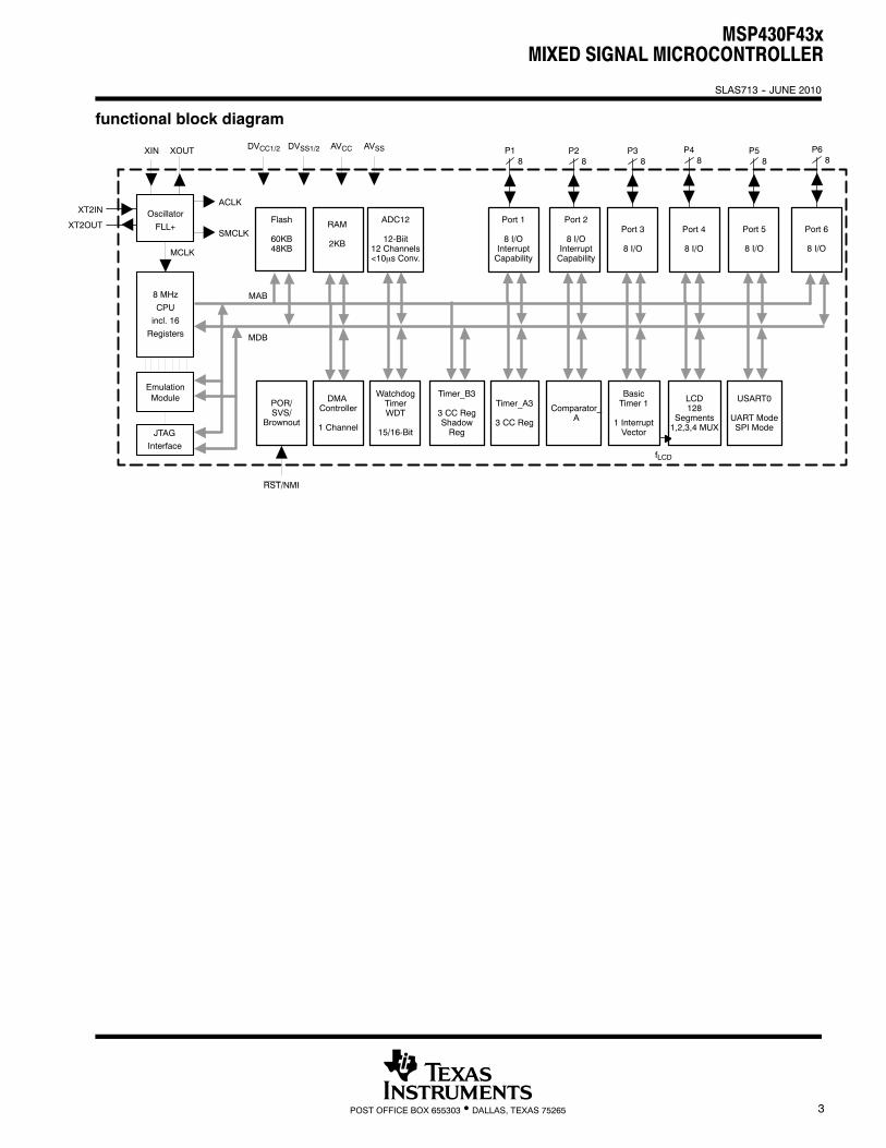
functional block diagram
Comparator_A
DVCC1/2 DVSS1/2 AVCC AVSS
RST/NMI
P2
Flash
60KB48KB
RAM
2KB
WatchdogTimerWDT
15/16-Bit
Port 2
8 I/OInterruptCapability
POR/SVS/
Brownout
BasicTimer 1
1 InterruptVector
LCD128
Segments1,2,3,4 MUX
fLCD
8
MCLK
XOUT
JTAGInterface
XIN
SMCLK
ACLK
MDB
MAB
Emulation
P3
Port 3
8 I/O
8
ModuleTimer_A3
3 CC Reg
P1
Port 1
8 I/OInterruptCapability
8P4
Port 4
8 I/O
8
Timer_B3
3 CC RegShadowReg
USART0
UART ModeSPI Mode
XT2IN
XT2OUTADC12
12-Biit12 Channels<10µs Conv.
OscillatorFLL+
8 MHzCPUincl. 16Registers
DMAController
1 Channel
P5
Port 5
8 I/O
8P6
Port 6
8 I/O
8
MSP430F43xMIXED SIGNAL MICROCONTROLLER
SLAS713 -- JUNE 2010
4 POST OFFICE BOX 655303 • DALLAS, TEXAS 75265
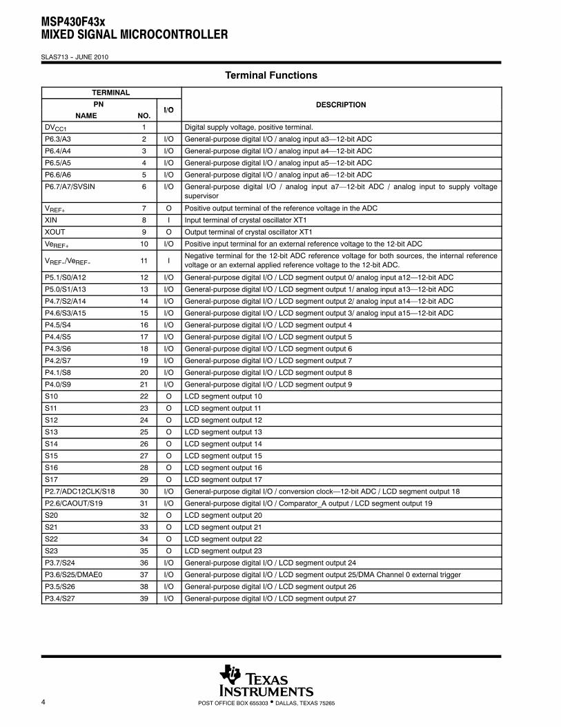
Terminal Functions
TERMINAL
PNI/O
DESCRIPTIONNAME NO.
I/ODESCRIPTION
DVCC1 1 Digital supply voltage, positive terminal.
P6.3/A3 2 I/O General-purpose digital I/O / analog input a3—12-bit ADC
P6.4/A4 3 I/O General-purpose digital I/O / analog input a4—12-bit ADC
P6.5/A5 4 I/O General-purpose digital I/O / analog input a5—12-bit ADC
P6.6/A6 5 I/O General-purpose digital I/O / analog input a6—12-bit ADC
P6.7/A7/SVSIN 6 I/O General-purpose digital I/O / analog input a7—12-bit ADC / analog input to supply voltagesupervisor
VREF+ 7 O Positive output terminal of the reference voltage in the ADC
XIN 8 I Input terminal of crystal oscillator XT1
XOUT 9 O Output terminal of crystal oscillator XT1
VeREF+ 10 I/O Positive input terminal for an external reference voltage to the 12-bit ADC
VREF--/VeREF-- 11 INegative terminal for the 12-bit ADC reference voltage for both sources, the internal referencevoltage or an external applied reference voltage to the 12-bit ADC.
P5.1/S0/A12 12 I/O General-purpose digital I/O / LCD segment output 0/ analog input a12—12-bit ADC
P5.0/S1/A13 13 I/O General-purpose digital I/O / LCD segment output 1/ analog input a13—12-bit ADC
P4.7/S2/A14 14 I/O General-purpose digital I/O / LCD segment output 2/ analog input a14—12-bit ADC
P4.6/S3/A15 15 I/O General-purpose digital I/O / LCD segment output 3/ analog input a15—12-bit ADC
P4.5/S4 16 I/O General-purpose digital I/O / LCD segment output 4
P4.4/S5 17 I/O General-purpose digital I/O / LCD segment output 5
P4.3/S6 18 I/O General-purpose digital I/O / LCD segment output 6
P4.2/S7 19 I/O General-purpose digital I/O / LCD segment output 7
P4.1/S8 20 I/O General-purpose digital I/O / LCD segment output 8
P4.0/S9 21 I/O General-purpose digital I/O / LCD segment output 9
S10 22 O LCD segment output 10
S11 23 O LCD segment output 11
S12 24 O LCD segment output 12
S13 25 O LCD segment output 13
S14 26 O LCD segment output 14
S15 27 O LCD segment output 15
S16 28 O LCD segment output 16
S17 29 O LCD segment output 17
P2.7/ADC12CLK/S18 30 I/O General-purpose digital I/O / conversion clock—12-bit ADC / LCD segment output 18
P2.6/CAOUT/S19 31 I/O General-purpose digital I/O / Comparator_A output / LCD segment output 19
S20 32 O LCD segment output 20
S21 33 O LCD segment output 21
S22 34 O LCD segment output 22
S23 35 O LCD segment output 23
P3.7/S24 36 I/O General-purpose digital I/O / LCD segment output 24
P3.6/S25/DMAE0 37 I/O General-purpose digital I/O / LCD segment output 25/DMA Channel 0 external trigger
P3.5/S26 38 I/O General-purpose digital I/O / LCD segment output 26
P3.4/S27 39 I/O General-purpose digital I/O / LCD segment output 27
MSP430F43xMIXED SIGNAL MICROCONTROLLER
SLAS713 -- JUNE 2010
5POST OFFICE BOX 655303 • DALLAS, TEXAS 75265
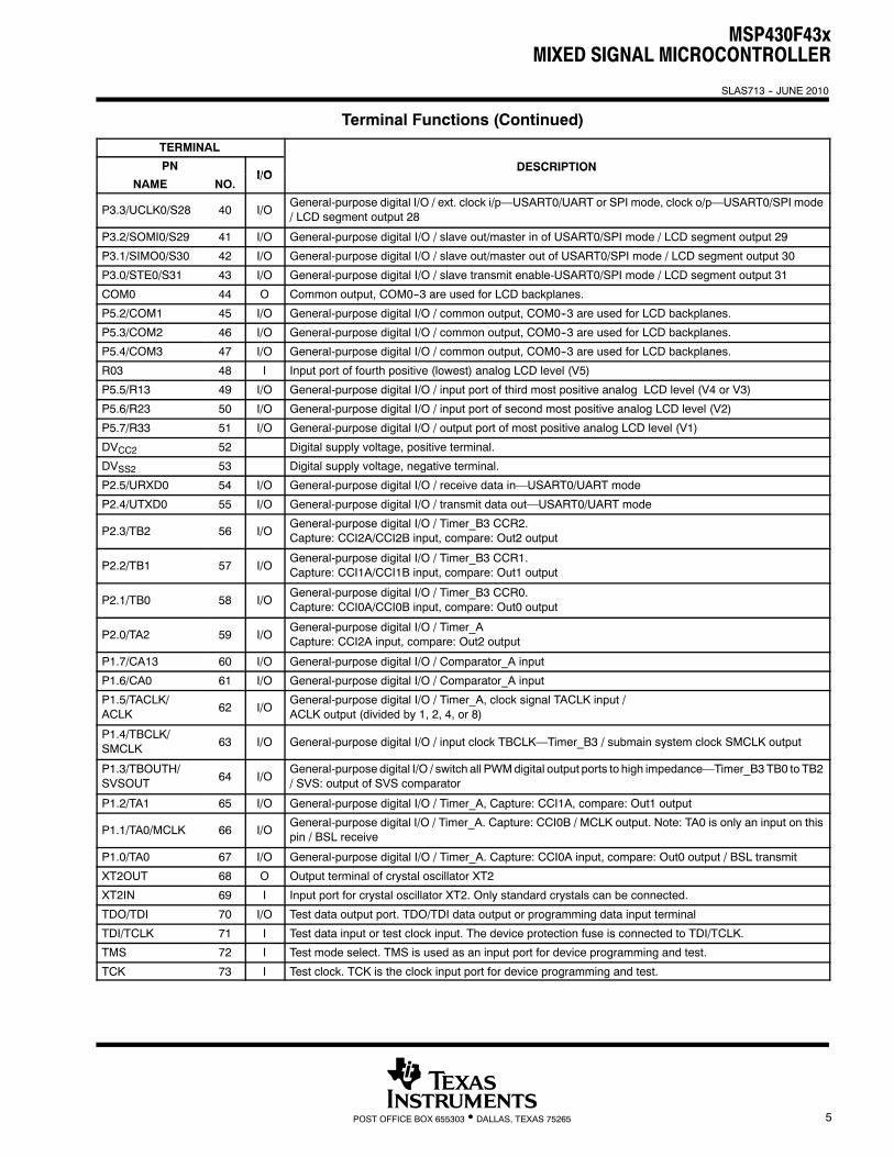
Terminal Functions (Continued)
TERMINAL
PNI/O
DESCRIPTIONNAME NO.
I/ODESCRIPTION
P3.3/UCLK0/S28 40 I/OGeneral-purpose digital I/O / ext. clock i/p—USART0/UART or SPI mode, clock o/p—USART0/SPI mode/ LCD segment output 28
P3.2/SOMI0/S29 41 I/O General-purpose digital I/O / slave out/master in of USART0/SPI mode / LCD segment output 29
P3.1/SIMO0/S30 42 I/O General-purpose digital I/O / slave out/master out of USART0/SPI mode / LCD segment output 30
P3.0/STE0/S31 43 I/O General-purpose digital I/O / slave transmit enable-USART0/SPI mode / LCD segment output 31
COM0 44 O Common output, COM0--3 are used for LCD backplanes.
P5.2/COM1 45 I/O General-purpose digital I/O / common output, COM0--3 are used for LCD backplanes.
P5.3/COM2 46 I/O General-purpose digital I/O / common output, COM0--3 are used for LCD backplanes.
P5.4/COM3 47 I/O General-purpose digital I/O / common output, COM0--3 are used for LCD backplanes.
R03 48 I Input port of fourth positive (lowest) analog LCD level (V5)
P5.5/R13 49 I/O General-purpose digital I/O / input port of third most positive analog LCD level (V4 or V3)
P5.6/R23 50 I/O General-purpose digital I/O / input port of second most positive analog LCD level (V2)
P5.7/R33 51 I/O General-purpose digital I/O / output port of most positive analog LCD level (V1)
DVCC2 52 Digital supply voltage, positive terminal.
DVSS2 53 Digital supply voltage, negative terminal.
P2.5/URXD0 54 I/O General-purpose digital I/O / receive data in—USART0/UART mode
P2.4/UTXD0 55 I/O General-purpose digital I/O / transmit data out—USART0/UART mode
P2.3/TB2 56 I/OGeneral-purpose digital I/O / Timer_B3 CCR2.Capture: CCI2A/CCI2B input, compare: Out2 output
P2.2/TB1 57 I/OGeneral-purpose digital I/O / Timer_B3 CCR1.Capture: CCI1A/CCI1B input, compare: Out1 output
P2.1/TB0 58 I/OGeneral-purpose digital I/O / Timer_B3 CCR0.Capture: CCI0A/CCI0B input, compare: Out0 output
P2.0/TA2 59 I/OGeneral-purpose digital I/O / Timer_ACapture: CCI2A input, compare: Out2 output
P1.7/CA13 60 I/O General-purpose digital I/O / Comparator_A input
P1.6/CA0 61 I/O General-purpose digital I/O / Comparator_A input
P1.5/TACLK/ACLK 62 I/O
General-purpose digital I/O / Timer_A, clock signal TACLK input /ACLK output (divided by 1, 2, 4, or 8)
P1.4/TBCLK/SMCLK 63 I/O General-purpose digital I/O / input clock TBCLK—Timer_B3 / submain system clock SMCLK output
P1.3/TBOUTH/SVSOUT 64 I/O
General-purpose digital I/O / switch all PWMdigital output ports to high impedance—Timer_B3TB0 to TB2/ SVS: output of SVS comparator
P1.2/TA1 65 I/O General-purpose digital I/O / Timer_A, Capture: CCI1A, compare: Out1 output
P1.1/TA0/MCLK 66 I/OGeneral-purpose digital I/O / Timer_A. Capture: CCI0B / MCLK output. Note: TA0 is only an input on thispin / BSL receive
P1.0/TA0 67 I/O General-purpose digital I/O / Timer_A. Capture: CCI0A input, compare: Out0 output / BSL transmit
XT2OUT 68 O Output terminal of crystal oscillator XT2
XT2IN 69 I Input port for crystal oscillator XT2. Only standard crystals can be connected.
TDO/TDI 70 I/O Test data output port. TDO/TDI data output or programming data input terminal
TDI/TCLK 71 I Test data input or test clock input. The device protection fuse is connected to TDI/TCLK.
TMS 72 I Test mode select. TMS is used as an input port for device programming and test.
TCK 73 I Test clock. TCK is the clock input port for device programming and test.
MSP430F43xMIXED SIGNAL MICROCONTROLLER
SLAS713 -- JUNE 2010
6 POST OFFICE BOX 655303 • DALLAS, TEXAS 75265
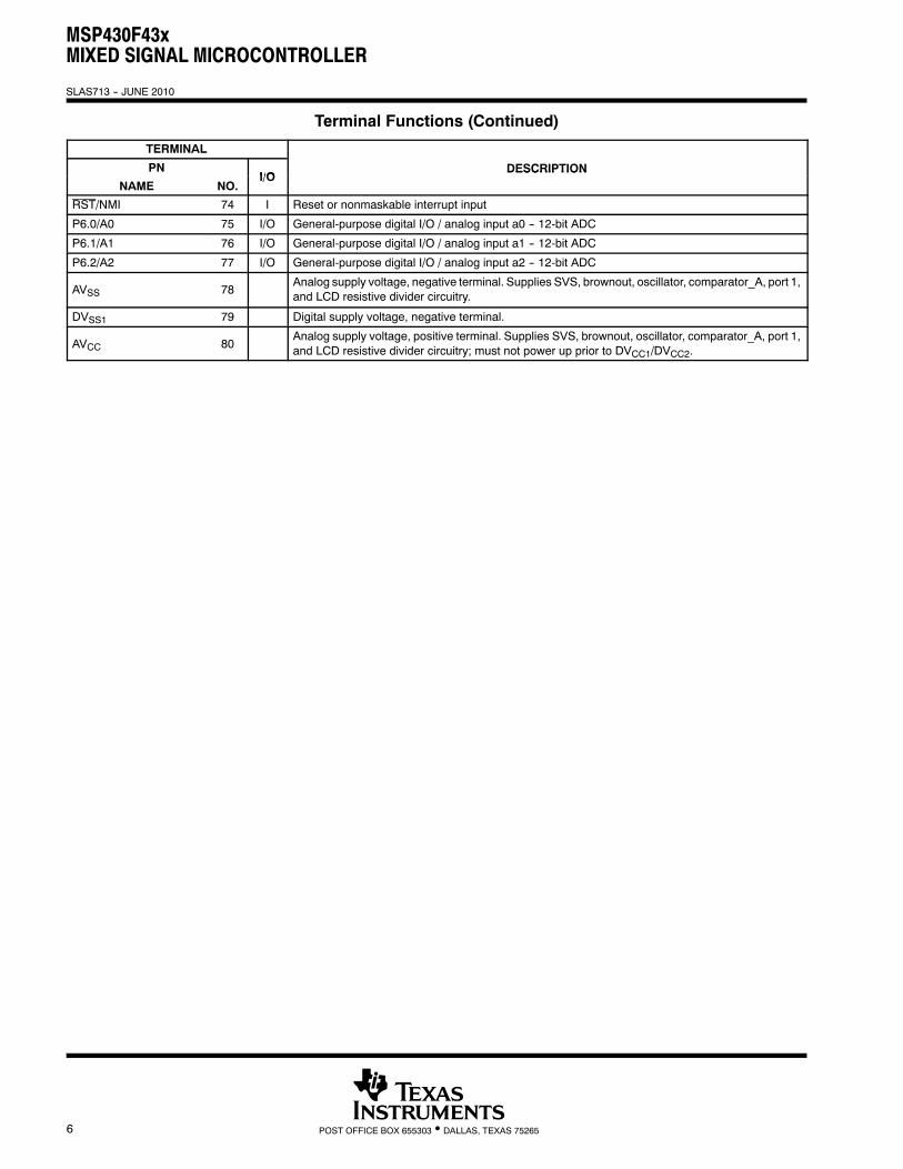
Terminal Functions (Continued)
TERMINAL
PNI/O
DESCRIPTIONNAME NO.
I/ODESCRIPTION
RST/NMI 74 I Reset or nonmaskable interrupt input
P6.0/A0 75 I/O General-purpose digital I/O / analog input a0 -- 12-bit ADC
P6.1/A1 76 I/O General-purpose digital I/O / analog input a1 -- 12-bit ADC
P6.2/A2 77 I/O General-purpose digital I/O / analog input a2 -- 12-bit ADC
AVSS 78Analog supply voltage, negative terminal. Supplies SVS, brownout, oscillator, comparator_A, port 1,and LCD resistive divider circuitry.
DVSS1 79 Digital supply voltage, negative terminal.
AVCC 80Analog supply voltage, positive terminal. Supplies SVS, brownout, oscillator, comparator_A, port 1,and LCD resistive divider circuitry; must not power up prior to DVCC1/DVCC2.
General-Purpose Register
Program Counter
Stack Pointer
Status Register
Constant Generator
General-Purpose Register
General-Purpose Register
General-Purpose Register
PC/R0
SP/R1
SR/CG1/R2
CG2/R3
R4
R5
R12
R13
General-Purpose Register
General-Purpose Register
R6
R7
General-Purpose Register
General-Purpose Register
R8
R9
General-Purpose Register
General-Purpose Register
R10
R11
General-Purpose Register
General-Purpose Register
R14
R15
MSP430F43xMIXED SIGNAL MICROCONTROLLER
SLAS713 -- JUNE 2010
7POST OFFICE BOX 655303 • DALLAS, TEXAS 75265
short-form description
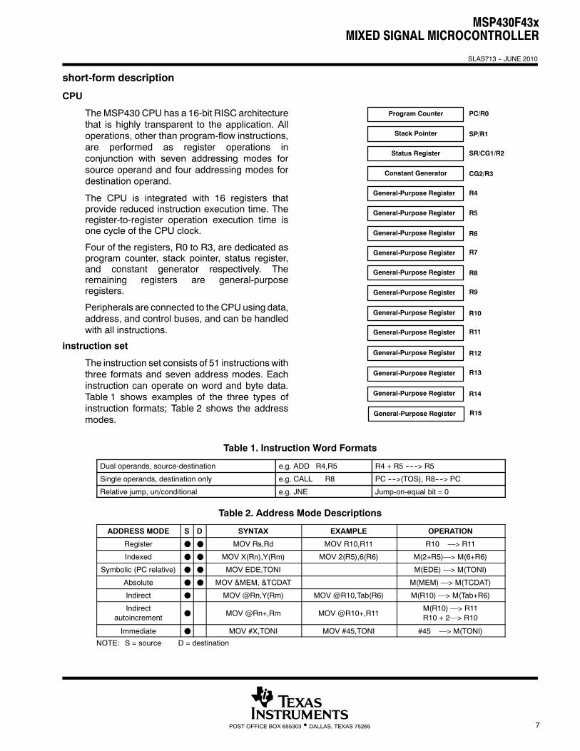
CPU
TheMSP430 CPU has a 16-bit RISC architecturethat is highly transparent to the application. Alloperations, other than program-flow instructions,are performed as register operations inconjunction with seven addressing modes forsource operand and four addressing modes fordestination operand.
The CPU is integrated with 16 registers thatprovide reduced instruction execution time. Theregister-to-register operation execution time isone cycle of the CPU clock.
Four of the registers, R0 to R3, are dedicated asprogram counter, stack pointer, status register,and constant generator respectively. Theremaining registers are general-purposeregisters.
Peripherals are connected to the CPU using data,address, and control buses, and can be handledwith all instructions.
instruction set
The instruction set consists of 51 instructions withthree formats and seven address modes. Eachinstruction can operate on word and byte data.Table 1 shows examples of the three types ofinstruction formats; Table 2 shows the addressmodes.
Table 1. Instruction Word Formats
Dual operands, source-destination e.g. ADD R4,R5 R4 + R5 ------> R5
Single operands, destination only e.g. CALL R8 PC ---->(TOS), R8----> PC
Relative jump, un/conditional e.g. JNE Jump-on-equal bit = 0
Table 2. Address Mode Descriptions
ADDRESS MODE S D SYNTAX EXAMPLE OPERATION
Register F F MOV Rs,Rd MOV R10,R11 R10 —> R11
Indexed F F MOV X(Rn),Y(Rm) MOV 2(R5),6(R6) M(2+R5)—> M(6+R6)
Symbolic (PC relative) F F MOV EDE,TONI M(EDE) —> M(TONI)
Absolute F F MOV &MEM, &TCDAT M(MEM) —> M(TCDAT)
Indirect F MOV @Rn,Y(Rm) MOV @R10,Tab(R6) M(R10) —> M(Tab+R6)
Indirectautoincrement F MOV @Rn+,Rm MOV @R10+,R11
M(R10) —> R11R10 + 2—> R10
Immediate F MOV #X,TONI MOV #45,TONI #45 —> M(TONI)
NOTE: S = source D = destination
MSP430F43xMIXED SIGNAL MICROCONTROLLER
SLAS713 -- JUNE 2010
8 POST OFFICE BOX 655303 • DALLAS, TEXAS 75265
operating modes
The MSP430 has one active mode and five software selectable low-power modes of operation. An interruptevent can wake up the device from any of the five low-power modes, service the request, and restore back tothe low-power mode on return from the interrupt program.
The following six operating modes can be configured by software:
D Active mode (AM)
-- All clocks are active
D Low-power mode 0 (LPM0)
-- CPU is disabled
-- ACLK and SMCLK remain active, MCLK is disabled
-- FLL+ loop control remains active
D Low-power mode 1 (LPM1)
-- CPU is disabled
-- FLL+ loop control is disabled
-- ACLK and SMCLK remain active, MCLK is disabled
D Low-power mode 2 (LPM2)
-- CPU is disabled
-- MCLK, FLL+ loop control, and DCOCLK are disabled
-- DCO’s dc-generator remains enabled
-- ACLK remains active
D Low-power mode 3 (LPM3)
-- CPU is disabled
-- MCLK, FLL+ loop control, and DCOCLK are disabled
-- DCO’s dc-generator is disabled
-- ACLK remains active
D Low-power mode 4 (LPM4)
-- CPU is disabled
-- ACLK is disabled
-- MCLK, FLL+ loop control, and DCOCLK are disabled
-- DCO’s dc-generator is disabled
-- Crystal oscillator is stopped
MSP430F43xMIXED SIGNAL MICROCONTROLLER
SLAS713 -- JUNE 2010
9POST OFFICE BOX 655303 • DALLAS, TEXAS 75265
interrupt vector addresses
The interrupt vectors and the power-up starting address are located in the address range 0FFFFh to 0FFE0h.The vector contains the 16-bit address of the appropriate interrupt-handler instruction sequence.
INTERRUPT SOURCE INTERRUPT FLAG SYSTEM INTERRUPTWORD
ADDRESS PRIORITY
Power-UpExternal ResetWatchdog
Flash Memory
WDTIFGKEYV
(see Note 1)
Reset 0FFFEh 15, highest
NMIOscillator Fault
Flash Memory Access Violation
NMIIFG (see Notes 1 and 3)OFIFG (see Notes 1 and 3)
ACCVIFG (see Notes 1 and 3)
(Non)maskable(Non)maskable(Non)maskable
0FFFCh 14
Timer_B3 TBCCR0 CCIFG0 (see Note 2) Maskable 0FFFAh 13
Timer_B3TBCCR1 CCIFG1, TBCCR2 CCIFG2,
TBIFG (see Notes 1 and 2) Maskable 0FFF8h 12
Comparator_A CAIFG Maskable 0FFF6h 11
Watchdog Timer WDTIFG Maskable 0FFF4h 10
USART0 Receive URXIFG0 Maskable 0FFF2h 9
USART0 Transmit UTXIFG0 Maskable 0FFF0h 8
ADC12 ADC12IFG (see Notes 1 and 2) Maskable 0FFEEh 7
Timer_A3 TACCR0 CCIFG0 (see Note 2) Maskable 0FFECh 6
Timer_A3TACCR1 CCIFG1 and TACCR2 CCIFG2,
TAIFG (see Notes 1 and 2) Maskable 0FFEAh 5
I/O Port P1 (Eight Flags) P1IFG.0 to P1IFG.7 (see Notes 1 and 2) Maskable 0FFE8h 4
DMA DMA0IFG (see Notes 1 and 2) Maskable 0FFE6h 3
0FFE4h 2
I/O Port P2 (Eight Flags) P2IFG.0 to P2IFG.7 (see Notes 1 and 2) Maskable 0FFE2h 1
Basic Timer1 BTIFG Maskable 0FFE0h 0, lowest
NOTES: 1. Multiple source flags2. Interrupt flags are located in the module.3. (Non)maskable: the individual interrupt-enable bit can disable an interrupt event, but the general-interrupt enable cannot disable
it.
MSP430F43xMIXED SIGNAL MICROCONTROLLER
SLAS713 -- JUNE 2010
10 POST OFFICE BOX 655303 • DALLAS, TEXAS 75265
special function registers
TheMSP430special function registers(SFR) are located in the lowest address spaceandareorganizedasbytemode registers. SFRs should be accessed with byte instructions.
interrupt enable 1 and 2
7 6 5 4 0
UTXIE0 OFIE WDTIE
3 2 1
rw–0 rw–0 rw–0
Address
0h URXIE0 ACCVIE NMIIE
rw–0 rw–0 rw–0
WDTIE: Watchdog timer interrupt enable. Inactive if watchdog mode is selected.Active if watchdog timer is configured as a general-purpose timer.
OFIE: Oscillator fault interrupt enable
NMIIE: Nonmaskable interrupt enable
ACCVIE: Flash access violation interrupt enable
URXIE0: USART0: UART and SPI receive-interrupt enable
UTXIE0: USART0: UART and SPI transmit-interrupt enable
7 6 5 4 03 2 1Address
01h
rw–0
BTIE
BTIE: Basic timer interrupt enable
interrupt flag register 1 and 2
7 6 5 4 0
UTXIFG0 OFIFG WDTIFG
3 2 1
rw–0 rw–1 rw–(0)
Address
02h URXIFG0 NMIIFG
rw–1 rw–0
WDTIFG: Set on watchdog timer overflow (in watchdog mode) or security key violationReset on VCC power-on or a reset condition at the RST/NMI pin in reset mode
OFIFG: Flag set on oscillator fault
NMIIFG: Set via RST/NMI pin
URXIFG0: USART0: UART and SPI receive flag
UTXIFG0: USART0: UART and SPI transmit flag
7 6 5 4 03 2 1Address
03h BTIFG
rw–0
BTIFG: Basic timer flag
MSP430F43xMIXED SIGNAL MICROCONTROLLER
SLAS713 -- JUNE 2010
11POST OFFICE BOX 655303 • DALLAS, TEXAS 75265
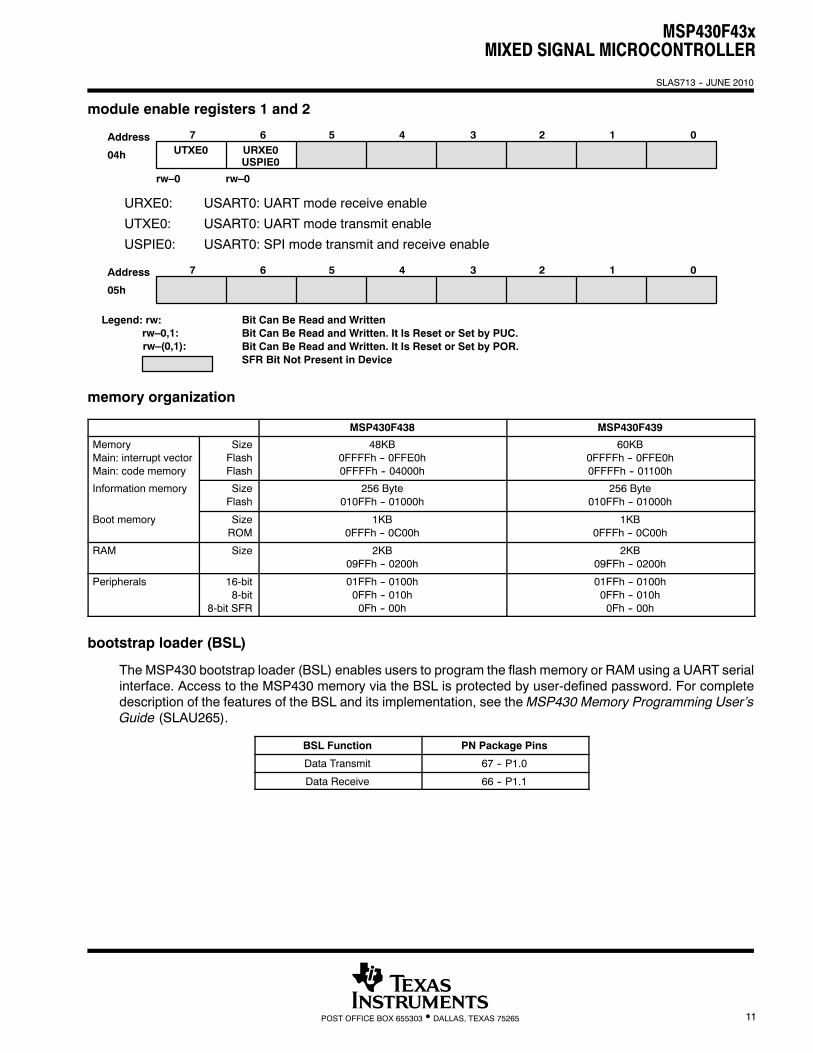
module enable registers 1 and 2
7 6 5 4 0UTXE0
3 2 1
rw–0 rw–0
Address
04h URXE0USPIE0
URXE0: USART0: UART mode receive enable
UTXE0: USART0: UART mode transmit enable
USPIE0: USART0: SPI mode transmit and receive enable
7 6 5 4 03 2 1Address
05h
rw–0,1:Legend: rw: Bit Can Be Read and Written
Bit Can Be Read and Written. It Is Reset or Set by PUC.Bit Can Be Read and Written. It Is Reset or Set by POR.SFR Bit Not Present in Device
rw–(0,1):
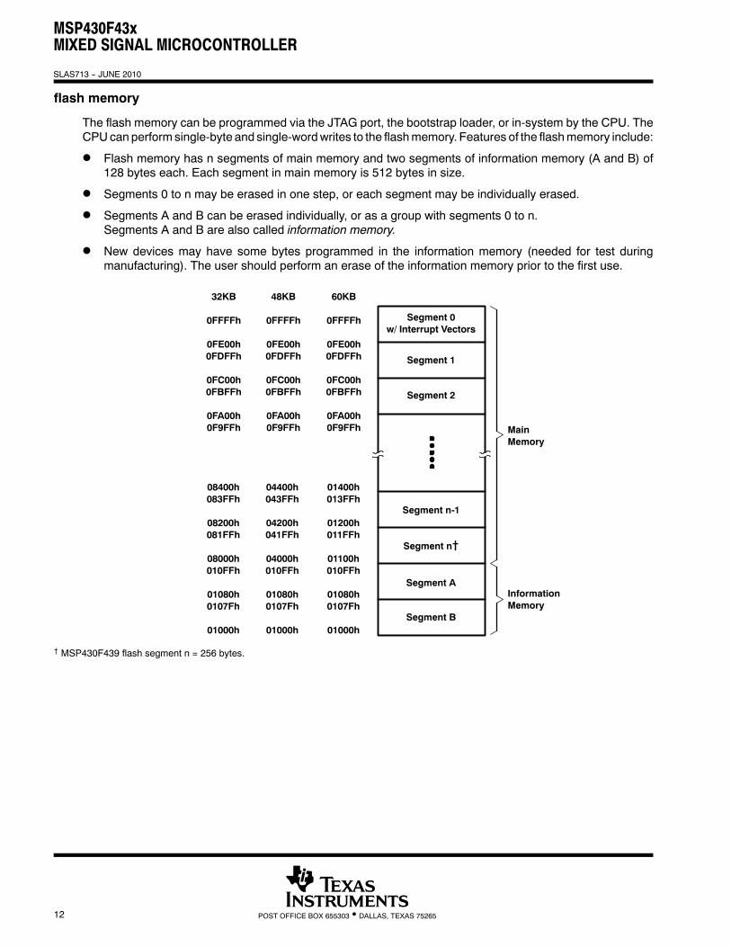
memory organization
MSP430F438 MSP430F439
MemoryMain: interrupt vectorMain: code memory
SizeFlashFlash
48KB0FFFFh -- 0FFE0h0FFFFh -- 04000h
60KB0FFFFh -- 0FFE0h0FFFFh -- 01100h
Information memory SizeFlash
256 Byte010FFh -- 01000h
256 Byte010FFh -- 01000h
Boot memory SizeROM
1KB0FFFh -- 0C00h
1KB0FFFh -- 0C00h
RAM Size 2KB09FFh -- 0200h
2KB09FFh -- 0200h
Peripherals 16-bit8-bit
8-bit SFR
01FFh -- 0100h0FFh -- 010h0Fh -- 00h
01FFh -- 0100h0FFh -- 010h0Fh -- 00h
bootstrap loader (BSL)
The MSP430 bootstrap loader (BSL) enables users to program the flash memory or RAM using a UART serialinterface. Access to the MSP430 memory via the BSL is protected by user-defined password. For completedescription of the features of the BSL and its implementation, see the MSP430 Memory Programming User’sGuide (SLAU265).
BSL Function PN Package Pins
Data Transmit 67 -- P1.0
Data Receive 66 -- P1.1
MSP430F43xMIXED SIGNAL MICROCONTROLLER
SLAS713 -- JUNE 2010
12 POST OFFICE BOX 655303 • DALLAS, TEXAS 75265
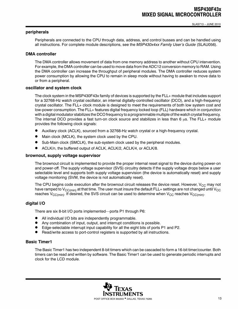
flash memory
The flash memory can be programmed via the JTAG port, the bootstrap loader, or in-system by the CPU. TheCPUcan performsingle-byte and single-wordwrites to the flashmemory. Features of the flashmemory include:
D Flash memory has n segments of main memory and two segments of information memory (A and B) of128 bytes each. Each segment in main memory is 512 bytes in size.
D Segments 0 to n may be erased in one step, or each segment may be individually erased.
D Segments A and B can be erased individually, or as a group with segments 0 to n.Segments A and B are also called information memory.
D New devices may have some bytes programmed in the information memory (needed for test duringmanufacturing). The user should perform an erase of the information memory prior to the first use.
Segment 0w/ Interrupt Vectors
Segment 1
Segment 2
Segment n-1
Segment n†
Segment A
Segment B
MainMemory
InformationMemory
32KB
0FFFFh
0FE00h0FDFFh
0FC00h0FBFFh
0FA00h0F9FFh
48KB
0FFFFh
0FE00h0FDFFh
0FC00h0FBFFh
0FA00h0F9FFh
60KB
0FFFFh
0FE00h0FDFFh
0FC00h0FBFFh
0FA00h0F9FFh
08400h083FFh
08200h081FFh
08000h010FFh
01080h0107Fh
01000h
04400h043FFh
04200h041FFh
04000h010FFh
01080h0107Fh
01000h
01400h013FFh
01200h011FFh
01100h010FFh
01080h0107Fh
01000h
† MSP430F439 flash segment n = 256 bytes.
MSP430F43xMIXED SIGNAL MICROCONTROLLER
SLAS713 -- JUNE 2010
13POST OFFICE BOX 655303 • DALLAS, TEXAS 75265
peripherals
Peripherals are connected to the CPU through data, address, and control busses and can be handled usingall instructions. For complete module descriptions, see the MSP430x4xx Family User’s Guide (SLAU056).
DMA controller
The DMA controller allows movement of data from one memory address to another without CPU intervention.For example, theDMAcontroller can be used tomove data from the ADC12 conversionmemory to RAM.Usingthe DMA controller can increase the throughput of peripheral modules. The DMA controller reduces systempower consumption by allowing the CPU to remain in sleep mode without having to awaken to move data toor from a peripheral.
oscillator and system clock
The clock system in the MSP430F43x family of devices is supported by the FLL+ module that includes supportfor a 32768-Hz watch crystal oscillator, an internal digitally-controlled oscillator (DCO), and a high-frequencycrystal oscillator. The FLL+ clock module is designed to meet the requirements of both low system cost andlow-power consumption. The FLL+ features digital frequency locked loop (FLL) hardware which in conjunctionwith adigitalmodulator stabilizes theDCO frequency to aprogrammablemultiple of thewatch crystal frequency.The internal DCO provides a fast turn-on clock source and stabilizes in less than 6 µs. The FLL+ moduleprovides the following clock signals:
D Auxiliary clock (ACLK), sourced from a 32768-Hz watch crystal or a high-frequency crystal.D Main clock (MCLK), the system clock used by the CPU.D Sub-Main clock (SMCLK), the sub-system clock used by the peripheral modules.D ACLK/n, the buffered output of ACLK, ACLK/2, ACLK/4, or ACLK/8.
brownout, supply voltage supervisor
The brownout circuit is implemented to provide the proper internal reset signal to the device during power-onand power-off. The supply voltage supervisor (SVS) circuitry detects if the supply voltage drops below a userselectable level and supports both supply voltage supervision (the device is automatically reset) and supplyvoltage monitoring (SVM, the device is not automatically reset).
The CPU begins code execution after the brownout circuit releases the device reset. However, VCC may nothave ramped to VCC(min) at that time. The user must insure the default FLL+ settings are not changed until VCCreaches VCC(min). If desired, the SVS circuit can be used to determine when VCC reaches VCC(min).
digital I/O
There are six 8-bit I/O ports implemented—ports P1 through P6:
D All individual I/O bits are independently programmable.D Any combination of input, output, and interrupt conditions is possible.D Edge-selectable interrupt input capability for all the eight bits of ports P1 and P2.D Read/write access to port-control registers is supported by all instructions.
Basic Timer1
The Basic Timer1 has two independent 8-bit timers which can be cascaded to form a 16-bit timer/counter. Bothtimers can be read and written by software. The Basic Timer1 can be used to generate periodic interrupts andclock for the LCD module.
MSP430F43xMIXED SIGNAL MICROCONTROLLER
SLAS713 -- JUNE 2010
14 POST OFFICE BOX 655303 • DALLAS, TEXAS 75265
LCD drive
The LCD driver generates the segment and common signals required to drive an LCD display. The LCDcontroller has dedicated data memory to hold segment drive information. Common and segment signals aregenerated as defined by the mode. Static, 2-MUX, 3-MUX, and 4-MUX LCDs are supported by this peripheral.
watchdog timer
The primary function of the watchdog timer (WDT) module is to perform a controlled system restart after asoftware problem occurs. If the selected time interval expires, a system reset is generated. If the watchdogfunction is not needed in an application, the module can be configured as an interval timer and can generateinterrupts at selected time intervals.
USART0
The MSP430F43x has one hardware universal synchronous/asynchronous receive transmit (USART)peripheral module that is used for serial data communication. The USART supports synchronous SPI (3 or 4pin) and asynchronous UART communication protocols, using double-buffered transmit and receive channels.
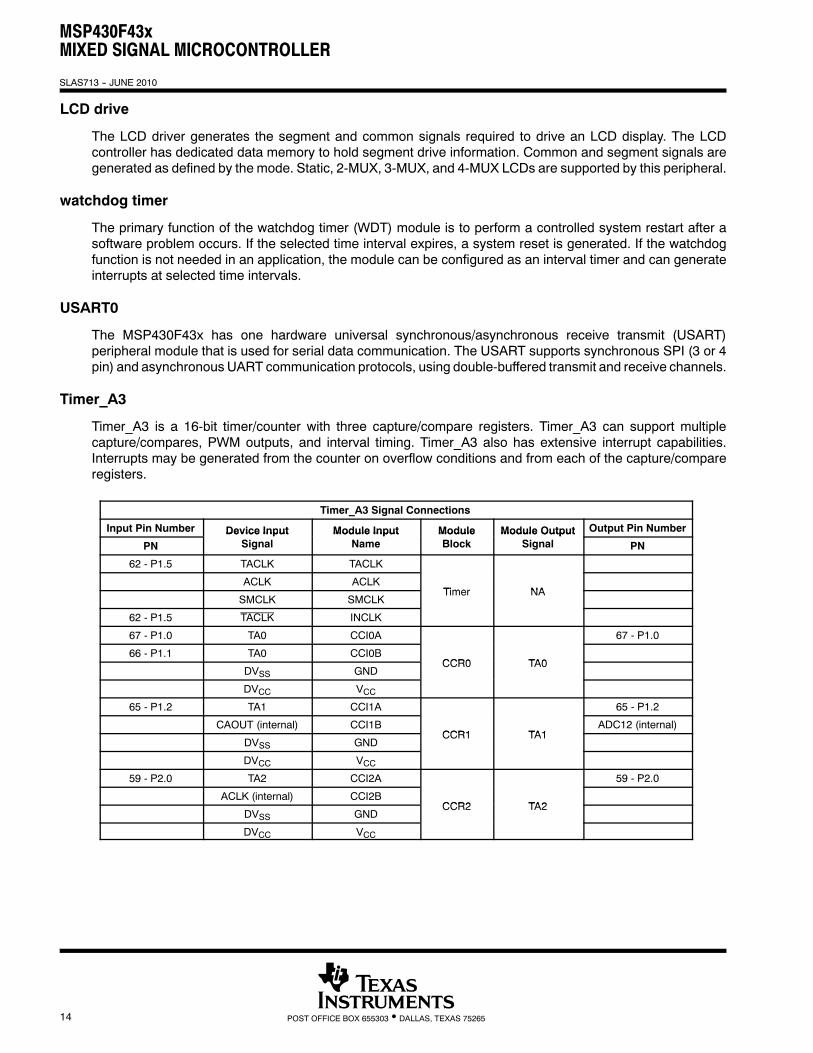
Timer_A3
Timer_A3 is a 16-bit timer/counter with three capture/compare registers. Timer_A3 can support multiplecapture/compares, PWM outputs, and interval timing. Timer_A3 also has extensive interrupt capabilities.Interrupts may be generated from the counter on overflow conditions and from each of the capture/compareregisters.
Timer_A3 Signal Connections
Input Pin Number Device Input Module Input Module Module Output Output Pin Number
PNDevice Input
SignalModule Input
NameModuleBlock
Module OutputSignal PN
62 - P1.5 TACLK TACLK
ACLK ACLKTimer NA
SMCLK SMCLKTimer NA
62 - P1.5 TACLK INCLK
67 - P1.0 TA0 CCI0A 67 - P1.0
66 - P1.1 TA0 CCI0BCCR0 TA0
DVSS GNDCCR0 TA0
DVCC VCC65 - P1.2 TA1 CCI1A 65 - P1.2
CAOUT (internal) CCI1BCCR1 TA1
ADC12 (internal)
DVSS GNDCCR1 TA1
DVCC VCC59 - P2.0 TA2 CCI2A 59 - P2.0
ACLK (internal) CCI2BCCR2 TA2
DVSS GNDCCR2 TA2
DVCC VCC
MSP430F43xMIXED SIGNAL MICROCONTROLLER
SLAS713 -- JUNE 2010
15POST OFFICE BOX 655303 • DALLAS, TEXAS 75265
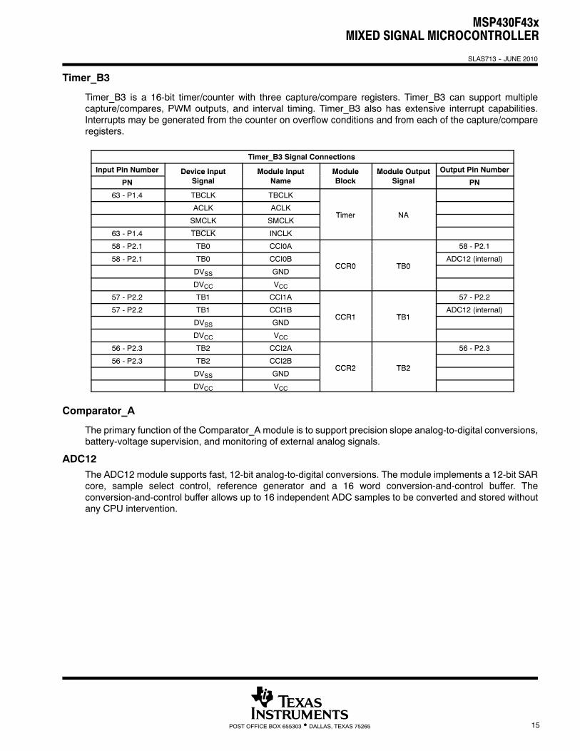
Timer_B3
Timer_B3 is a 16-bit timer/counter with three capture/compare registers. Timer_B3 can support multiplecapture/compares, PWM outputs, and interval timing. Timer_B3 also has extensive interrupt capabilities.Interrupts may be generated from the counter on overflow conditions and from each of the capture/compareregisters.
Timer_B3 Signal Connections
Input Pin Number Device Input Module Input Module Module Output Output Pin Number
PNDevice Input
SignalModule Input
NameModuleBlock
Module OutputSignal PN
63 - P1.4 TBCLK TBCLK
ACLK ACLKTimer NA
SMCLK SMCLKTimer NA
63 - P1.4 TBCLK INCLK
58 - P2.1 TB0 CCI0A 58 - P2.1
58 - P2.1 TB0 CCI0BCCR0 TB0
ADC12 (internal)
DVSS GNDCCR0 TB0
DVCC VCC57 - P2.2 TB1 CCI1A 57 - P2.2
57 - P2.2 TB1 CCI1BCCR1 TB1
ADC12 (internal)
DVSS GNDCCR1 TB1
DVCC VCC56 - P2.3 TB2 CCI2A 56 - P2.3
56 - P2.3 TB2 CCI2BCCR2 TB2
DVSS GNDCCR2 TB2
DVCC VCC
Comparator_A
The primary function of the Comparator_A module is to support precision slope analog-to-digital conversions,battery-voltage supervision, and monitoring of external analog signals.
ADC12The ADC12 module supports fast, 12-bit analog-to-digital conversions. The module implements a 12-bit SARcore, sample select control, reference generator and a 16 word conversion-and-control buffer. Theconversion-and-control buffer allows up to 16 independent ADC samples to be converted and stored withoutany CPU intervention.
MSP430F43xMIXED SIGNAL MICROCONTROLLER
SLAS713 -- JUNE 2010
16 POST OFFICE BOX 655303 • DALLAS, TEXAS 75265
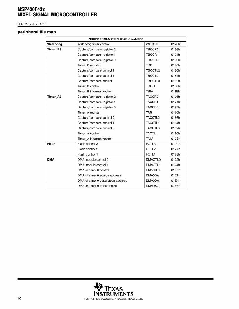
peripheral file map
PERIPHERALS WITH WORD ACCESS
Watchdog Watchdog timer control WDTCTL 0120h
Timer_B3 Capture/compare register 2 TBCCR2 0196h_
Capture/compare register 1 TBCCR1 0194h
Capture/compare register 0 TBCCR0 0192h
Timer_B register TBR 0190h
Capture/compare control 2 TBCCTL2 0186h
Capture/compare control 1 TBCCTL1 0184h
Capture/compare control 0 TBCCTL0 0182h
Timer_B control TBCTL 0180h
Timer_B interrupt vector TBIV 011Eh
Timer_A3 Capture/compare register 2 TACCR2 0176h_
Capture/compare register 1 TACCR1 0174h
Capture/compare register 0 TACCR0 0172h
Timer_A register TAR 0170h
Capture/compare control 2 TACCTL2 0166h
Capture/compare control 1 TACCTL1 0164h
Capture/compare control 0 TACCTL0 0162h
Timer_A control TACTL 0160h
Timer_A interrupt vector TAIV 012Eh
Flash Flash control 3 FCTL3 012Ch
Flash control 2 FCTL2 012Ah
Flash control 1 FCTL1 0128h
DMA DMA module control 0 DMACTL0 0122h
DMA module control 1 DMACTL1 0124h
DMA channel 0 control DMA0CTL 01E0h
DMA channel 0 source address DMA0SA 01E2h
DMA channel 0 destination address DMA0DA 01E4h
DMA channel 0 transfer size DMA0SZ 01E6h
MSP430F43xMIXED SIGNAL MICROCONTROLLER
SLAS713 -- JUNE 2010
17POST OFFICE BOX 655303 • DALLAS, TEXAS 75265
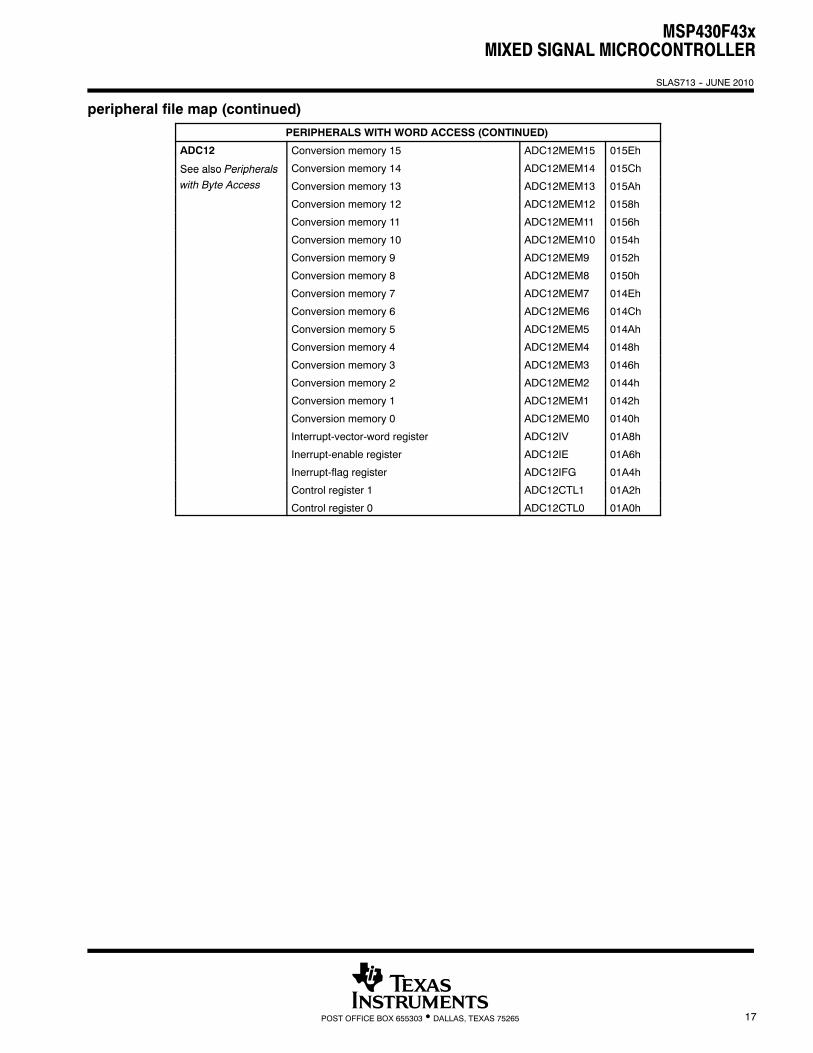
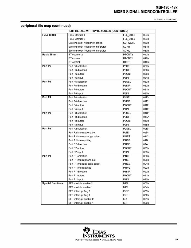
peripheral file map (continued)
PERIPHERALS WITH WORD ACCESS (CONTINUED)
ADC12 Conversion memory 15 ADC12MEM15 015Eh
See also Peripherals Conversion memory 14 ADC12MEM14 015ChSee also Peripheralswith Byte Access Conversion memory 13 ADC12MEM13 015Ahy
Conversion memory 12 ADC12MEM12 0158h
Conversion memory 11 ADC12MEM11 0156h
Conversion memory 10 ADC12MEM10 0154h
Conversion memory 9 ADC12MEM9 0152h
Conversion memory 8 ADC12MEM8 0150h
Conversion memory 7 ADC12MEM7 014Eh
Conversion memory 6 ADC12MEM6 014Ch
Conversion memory 5 ADC12MEM5 014Ah
Conversion memory 4 ADC12MEM4 0148h
Conversion memory 3 ADC12MEM3 0146h
Conversion memory 2 ADC12MEM2 0144h
Conversion memory 1 ADC12MEM1 0142h
Conversion memory 0 ADC12MEM0 0140h
Interrupt-vector-word register ADC12IV 01A8h
Inerrupt-enable register ADC12IE 01A6h
Inerrupt-flag register ADC12IFG 01A4h
Control register 1 ADC12CTL1 01A2h
Control register 0 ADC12CTL0 01A0h
MSP430F43xMIXED SIGNAL MICROCONTROLLER
SLAS713 -- JUNE 2010
18 POST OFFICE BOX 655303 • DALLAS, TEXAS 75265
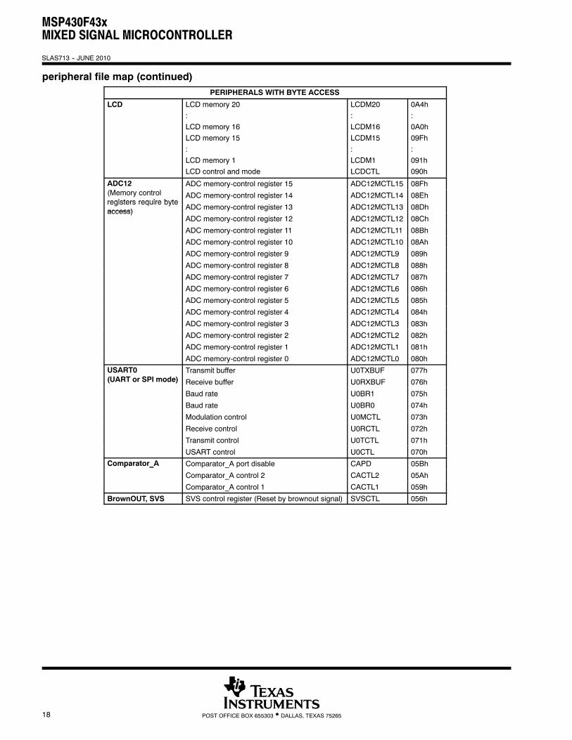
peripheral file map (continued)PERIPHERALS WITH BYTE ACCESS
LCD LCD memory 20:LCD memory 16LCD memory 15:LCD memory 1LCD control and mode
LCDM20:LCDM16LCDM15:LCDM1LCDCTL
0A4h:0A0h09Fh:091h090h
ADC12 ADC memory-control register 15 ADC12MCTL15 08Fh(Memory controlregisters require byte
ADC memory-control register 14 ADC12MCTL14 08Ehregisters require byteaccess) ADC memory-control register 13 ADC12MCTL13 08Dhaccess)
ADC memory-control register 12 ADC12MCTL12 08Ch
ADC memory-control register 11 ADC12MCTL11 08Bh
ADC memory-control register 10 ADC12MCTL10 08Ah
ADC memory-control register 9 ADC12MCTL9 089h
ADC memory-control register 8 ADC12MCTL8 088h
ADC memory-control register 7 ADC12MCTL7 087h
ADC memory-control register 6 ADC12MCTL6 086h
ADC memory-control register 5 ADC12MCTL5 085h
ADC memory-control register 4 ADC12MCTL4 084h
ADC memory-control register 3 ADC12MCTL3 083h
ADC memory-control register 2 ADC12MCTL2 082h
ADC memory-control register 1 ADC12MCTL1 081h
ADC memory-control register 0 ADC12MCTL0 080h
USART0 Transmit buffer U0TXBUF 077h(UART or SPI mode) Receive buffer U0RXBUF 076h
Baud rate U0BR1 075h
Baud rate U0BR0 074h
Modulation control U0MCTL 073h
Receive control U0RCTL 072h
Transmit control U0TCTL 071h
USART control U0CTL 070h
Comparator_A Comparator_A port disable CAPD 05Bhp _
Comparator_A control 2 CACTL2 05Ah
Comparator_A control 1 CACTL1 059h
BrownOUT, SVS SVS control register (Reset by brownout signal) SVSCTL 056h
MSP430F43xMIXED SIGNAL MICROCONTROLLER
SLAS713 -- JUNE 2010
19POST OFFICE BOX 655303 • DALLAS, TEXAS 75265
peripheral file map (continued)PERIPHERALS WITH BYTE ACCESS (CONTINUED)
FLL+ Clock FLL+ Control 1 FLL_CTL1 054h
FLL+ Control 0 FLL_CTL0 053h
System clock frequency control SCFQCTL 052h
System clock frequency integrator SCFI1 051h
System clock frequency integrator SCFI0 050h
Basic Timer1 BT counter 2BT counter 1BT control
BTCNT2BTCNT1BTCTL
047h046h040h
Port P6 Port P6 selection P6SEL 037h
Port P6 direction P6DIR 036h
Port P6 output P6OUT 035h
Port P6 input P6IN 034h
Port P5 Port P5 selection P5SEL 033h
Port P5 direction P5DIR 032h
Port P5 output P5OUT 031h
Port P5 input P5IN 030h
Port P4 Port P4 selection P4SEL 01Fh
Port P4 direction P4DIR 01Eh
Port P4 output P4OUT 01Dh
Port P4 input P4IN 01Ch
Port P3 Port P3 selection P3SEL 01Bh
Port P3 direction P3DIR 01Ah
Port P3 output P3OUT 019h
Port P3 input P3IN 018h
Port P2 Port P2 selection P2SEL 02Eh
Port P2 interrupt enable P2IE 02Dh
Port P2 interrupt-edge select P2IES 02Ch
Port P2 interrupt flag P2IFG 02Bh
Port P2 direction P2DIR 02Ah
Port P2 output P2OUT 029h
Port P2 input P2IN 028h
Port P1 Port P1 selection P1SEL 026h
Port P1 interrupt enable P1IE 025h
Port P1 interrupt-edge select P1IES 024h
Port P1 interrupt flag P1IFG 023h
Port P1 direction P1DIR 022h
Port P1 output P1OUT 021h
Port P1 input P1IN 020h
Special functions SFR module enable 2 ME2 005hp
SFR module enable 1 ME1 004h
SFR interrupt flag 2 IFG2 003h
SFR interrupt flag 1 IFG1 002h
SFR interrupt enable 2 IE2 001h
SFR interrupt enable 1 IE1 000h
MSP430F43xMIXED SIGNAL MICROCONTROLLER
SLAS713 -- JUNE 2010
20 POST OFFICE BOX 655303 • DALLAS, TEXAS 75265
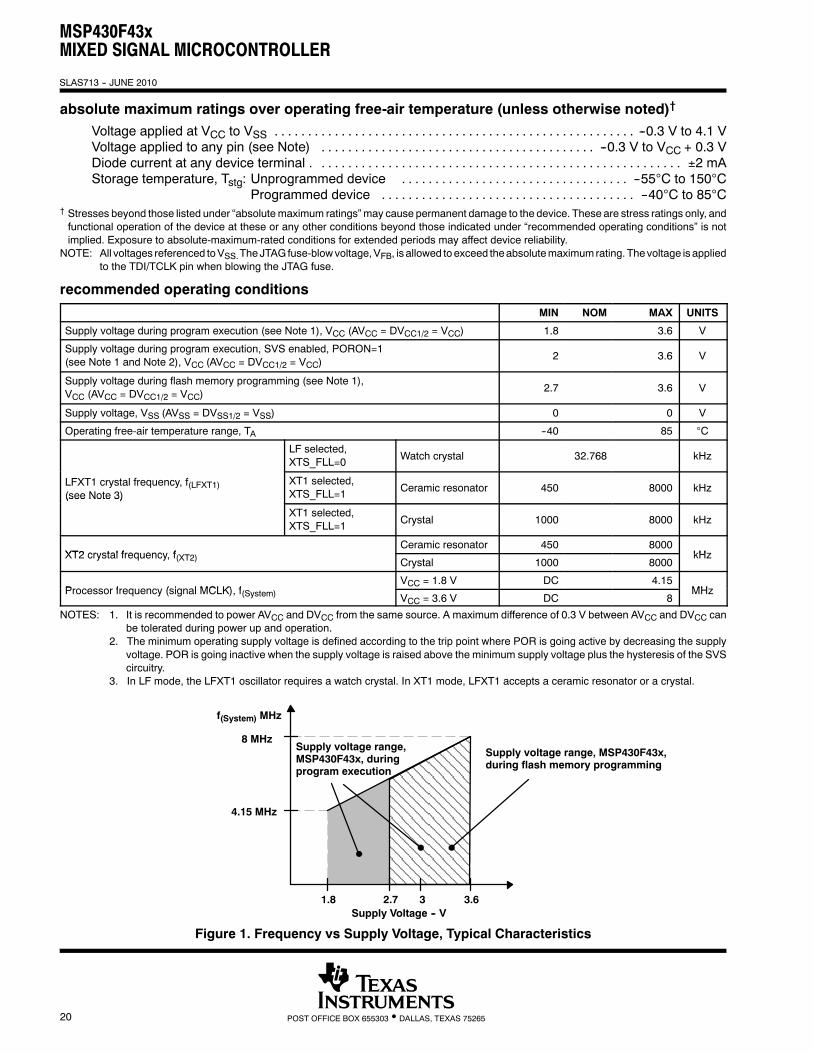
absolute maximum ratings over operating free-air temperature (unless otherwise noted)†
Voltage applied at VCC to VSS --0.3 V to 4.1 V. . . . . . . . . . . . . . . . . . . . . . . . . . . . . . . . . . . . . . . . . . . . . . . . . . . . . .Voltage applied to any pin (see Note) --0.3 V to VCC + 0.3 V. . . . . . . . . . . . . . . . . . . . . . . . . . . . . . . . . . . . . . . . .Diode current at any device terminal . ±2 mA. . . . . . . . . . . . . . . . . . . . . . . . . . . . . . . . . . . . . . . . . . . . . . . . . . . . . .Storage temperature, Tstg: Unprogrammed device --55°C to 150°C. . . . . . . . . . . . . . . . . . . . . . . . . . . . . . . . . .
Programmed device --40°C to 85°C. . . . . . . . . . . . . . . . . . . . . . . . . . . . . . . . . . . . . .† Stresses beyond those listed under “absolutemaximum ratings”may cause permanent damage to the device. These are stress ratings only, andfunctional operation of the device at these or any other conditions beyond those indicated under “recommended operating conditions” is notimplied. Exposure to absolute-maximum-rated conditions for extended periods may affect device reliability.
NOTE: All voltages referenced toVSS.The JTAG fuse-blowvoltage,VFB, is allowed toexceed theabsolutemaximumrating. Thevoltage is appliedto the TDI/TCLK pin when blowing the JTAG fuse.
recommended operating conditions
MIN NOM MAX UNITS
Supply voltage during program execution (see Note 1), VCC (AVCC = DVCC1/2 = VCC) 1.8 3.6 V
Supply voltage during program execution, SVS enabled, PORON=1(see Note 1 and Note 2), VCC (AVCC = DVCC1/2 = VCC)
2 3.6 V
Supply voltage during flash memory programming (see Note 1),VCC (AVCC = DVCC1/2 = VCC)
2.7 3.6 V
Supply voltage, VSS (AVSS = DVSS1/2 = VSS) 0 0 V
Operating free-air temperature range, TA --40 85 °C
LF selected,XTS_FLL=0 Watch crystal 32.768 kHz
LFXT1 crystal frequency, f(LFXT1)(see Note 3)
XT1 selected,XTS_FLL=1 Ceramic resonator 450 8000 kHz
(see Note 3)
XT1 selected,XTS_FLL=1 Crystal 1000 8000 kHz
XT2 cr stal freq enc fCeramic resonator 450 8000
kHXT2 crystal frequency, f(XT2) Crystal 1000 8000kHz
Processor freq enc (signal MCLK) fVCC = 1.8 V DC 4.15
MHProcessor frequency (signal MCLK), f(System) VCC = 3.6 V DC 8MHz
NOTES: 1. It is recommended to power AVCC and DVCC from the same source. A maximum difference of 0.3 V between AVCC and DVCC canbe tolerated during power up and operation.
2. The minimum operating supply voltage is defined according to the trip point where POR is going active by decreasing the supplyvoltage. POR is going inactive when the supply voltage is raised above the minimum supply voltage plus the hysteresis of the SVScircuitry.
3. In LF mode, the LFXT1 oscillator requires a watch crystal. In XT1 mode, LFXT1 accepts a ceramic resonator or a crystal.
1.8 3.62.7 3
4.15 MHz
8 MHz
Supply Voltage -- V
Supply voltage range, MSP430F43x,during flash memory programming
Supply voltage range,MSP430F43x, duringprogram execution
f(System) MHz
Figure 1. Frequency vs Supply Voltage, Typical Characteristics
MSP430F43xMIXED SIGNAL MICROCONTROLLER
SLAS713 -- JUNE 2010
21POST OFFICE BOX 655303 • DALLAS, TEXAS 75265
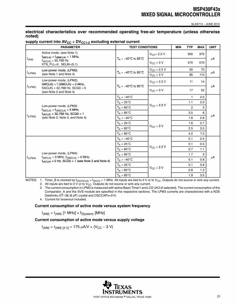
electrical characteristics over recommended operating free-air temperature (unless otherwisenoted)supply current into AVCC + DVCC1/2 excluding external current
PARAMETER TEST CONDITIONS MIN TYP MAX UNIT
I
Active mode, (see Note 1)f(MCLK) = f(SMCLK) = 1 MHz, T 40°C to 85°C
VCC= 2.2 V 300 370AI(AM)
f(MCLK) = f(SMCLK) = 1 MHz,f(ACLK) = 32,768 HzXTS_FLL=0, SELM=(0,1)
TA = --40°C to 85°CVCC = 3 V 470 570
µA
ILow-power mode, (LPM0)
T 40°C to 85°CVCC = 2.2 V 55 70
AI(LPM0)Low power mode, (LPM0)(see Note 1 and Note 4) TA = --40°C to 85°C
VCC = 3 V 95 110µA
I
Low-power mode, (LPM2),f(MCLK) = f (SMCLK) = 0 MHz,
T 40°C to 85°CVCC = 2.2 V 11 14
AI(LPM2)f(MCLK) = f (SMCLK) = 0 MHz,f(ACLK) = 32,768 Hz, SCG0 = 0(see Note 2 and Note 4)
TA = --40°C to 85°CVCC = 3 V 17 22
µA
TA = --40°C 1 2.0
TA = 25°CV 2 2 V
1.1 2.0Low-power mode, (LPM3)f(MCLK) = f(SMCLK) = 0 MHz
TA = 60°CVCC = 2.2 V 2 3
I
f(MCLK) = f(SMCLK) = 0 MHz,f(ACLK) = 32,768 Hz, SCG0 = 1 TA = 85°C 3.5 6
AI(LPM3)f(ACLK) = 32,768 Hz, SCG0 = 1(see Note 2, Note 3, and Note 4) TA = --40°C 1.8 2.8
µA( , , )
TA = 25°CV 3 V
1.6 2.7
TA = 60°CVCC = 3 V 2.5 3.5
TA = 85°C 4.2 7.5
TA = --40°C 0.1 0.5
TA = 25°CV 2 2 V
0.1 0.5
TA = 60°CVCC = 2.2 V 0.7 1.1
ILow-power mode, (LPM4)f 0 MHz f 0 MHz
TA = 85°C 1.7 3AI(LPM4) f(MCLK) = 0 MHz, f(SMCLK) = 0 MHz,
f(ACLK) = 0 Hz, SCG0 = 1 (see Note 2 and Note 4)TA = --40°C 0.1 0.8
µAf(ACLK) = 0 Hz, SCG0 = 1 (see Note 2 and Note 4)
TA = 25°CV 3 V
0.1 0.8
TA = 60°CVCC = 3 V 0.8 1.2
TA = 85°C 1.9 3.5
NOTES: 1. Timer_B is clocked by f(DCOCLK) = f(DCO) = 1 MHz. All inputs are tied to 0 V or to VCC. Outputs do not source or sink any current.2. All inputs are tied to 0 V or to VCC. Outputs do not source or sink any current.3. The current consumption in LPM3 is measured with active Basic Timer1 and LCD (ACLK selected). The current consumption of the
Comparator_A and the SVS module are specified in the respective sections. The LPM3 currents are characterized with a KDSDaishinku DT--38 (6 pF) crystal and OSCCAPx=01h.
4. Current for brownout included.
Current consumption of active mode versus system frequency
I(AM) = I(AM) [1 MHz] × f(System) [MHz]
Current consumption of active mode versus supply voltage
I(AM) = I(AM) [3 V] + 175 µA/V × (VCC – 3 V)
MSP430F43xMIXED SIGNAL MICROCONTROLLER
SLAS713 -- JUNE 2010
22 POST OFFICE BOX 655303 • DALLAS, TEXAS 75265
electrical characteristics over recommended operating free-air temperature (unless otherwisenoted) (continued)
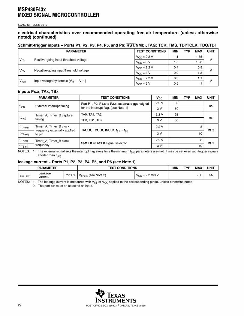
Schmitt-trigger inputs -- Ports P1, P2, P3, P4, P5, and P6; RST/NMI; JTAG: TCK, TMS, TDI/TCLK, TDO/TDIPARAMETER TEST CONDITIONS MIN TYP MAX UNIT
V Positi e going inp t threshold oltageVCC = 2.2 V 1.1 1.55
VVIT+ Positive-going input threshold voltageVCC = 3 V 1.5 1.98
V
V Negati e going inp t threshold oltageVCC = 2.2 V 0.4 0.9
VVIT-- Negative-going input threshold voltageVCC = 3 V 0.9 1.3
V
V Input voltage hysteresis (V V )VCC = 2.2 V 0.3 1.1
VVhys Input voltage hysteresis (VIT+ -- VIT--)VCC = 3 V 0.5 1
V
inputs Px.x, TAx, TBxPARAMETER TEST CONDITIONS VCC MIN TYP MAX UNIT
t External interrupt timingPort P1, P2: P1.x to P2.x, external trigger signal 2.2 V 62
nst(int) External interrupt timingPort P1, P2: P1.x to P2.x, external trigger signalfor the interrupt flag, (see Note 1) 3 V 50
ns
tTimer_A, Timer_B capture TA0, TA1, TA2 2.2 V 62
nst(cap)Timer_A, Timer_B capturetiming TB0, TB1, TB2 3 V 50
ns
f(TAext) Timer_A, Timer_B clockfrequency externally applied TACLK TBCLK INCLK: t t
2.2 V 8MHz
f(TBext)frequency externally appliedto pin
TACLK, TBCLK, INCLK: t(H) = t(L)3 V 10
MHz
f(TAint) Timer_A, Timer_B clockSMCLK or ACLK signal selected
2.2 V 8MHz
f(TBint)
Timer_A, Timer_B clockfrequency SMCLK or ACLK signal selected
3 V 10MHz
NOTES: 1. The external signal sets the interrupt flag every time the minimum t(int) parameters are met. It may be set even with trigger signalsshorter than t(int).
leakage current -- Ports P1, P2, P3, P4, P5, and P6 (see Note 1)PARAMETER TEST CONDITIONS MIN TYP MAX UNIT
Ilkg(Px.y)Leakagecurrent Port Px V(Px.y) (see Note 2) VCC = 2.2 V/3 V ±50 nA
NOTES: 1. The leakage current is measured with VSS or VCC applied to the corresponding pin(s), unless otherwise noted.2. The port pin must be selected as input.
MSP430F43xMIXED SIGNAL MICROCONTROLLER
SLAS713 -- JUNE 2010
23POST OFFICE BOX 655303 • DALLAS, TEXAS 75265
electrical characteristics over recommended operating free-air temperature (unless otherwisenoted) (continued)
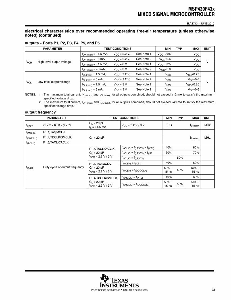
outputs -- Ports P1, P2, P3, P4, P5, and P6PARAMETER TEST CONDITIONS MIN TYP MAX UNIT
IOH(max) = --1.5 mA, VCC = 2.2 V, See Note 1 VCC--0.25 VCC
V High le el o tp t oltageIOH(max) = --6 mA, VCC = 2.2 V, See Note 2 VCC--0.6 VCC
VVOH High-level output voltageIOH(max) = --1.5 mA, VCC = 3 V, See Note 1 VCC--0.25 VCC
V
IOH(max) = --6 mA, VCC = 3 V, See Note 2 VCC--0.6 VCCIOL(max) = 1.5 mA, VCC = 2.2 V, See Note 1 VSS VSS+0.25
V Low level output voltageIOL(max) = 6 mA, VCC = 2.2 V, See Note 2 VSS VSS+0.6
VVOL Low-level output voltageIOL(max) = 1.5 mA, VCC = 3 V, See Note 1 VSS VSS+0.25
V
IOL(max) = 6 mA, VCC = 3 V, See Note 2 VSS VSS+0.6
NOTES: 1. The maximum total current, IOH(max) and IOL(max), for all outputs combined, should not exceed ±12 mA to satisfy the maximumspecified voltage drop.
2. The maximum total current, IOH(max) and IOL(max), for all outputs combined, should not exceed ±48 mA to satisfy the maximumspecified voltage drop.
output frequencyPARAMETER TEST CONDITIONS MIN TYP MAX UNIT
f(Px.y) (1 ≤ x ≤ 6, 0 ≤ y ≤ 7)CL = 20 pF,IL = ±1.5 mA VCC = 2.2 V / 3 V DC fSystem MHz
f(MCLK) P1.1/TA0/MCLK,
f(SMCLK) P1.4/TBCLK/SMCLK, CL = 20 pF fSystem MHz
f(ACLK) P1.5/TACLK/ACLK
CL 20 pF fSystem MHz
P1.5/TACLK/ACLK, f(ACLK) = f(LFXT1) = f(XT1) 40% 60%P1.5/TACLK/ACLK,CL = 20 pF f(ACLK) = f(LFXT1) = f(LF) 30% 70%CL 20 pFVCC = 2.2 V / 3 V f(ACLK) = f(LFXT1) 50%
P1.1/TA0/MCLK, f(MCLK) = f(XT1) 40% 60%t(Xdc) Duty cycle of output frequency
P1.1/TA0/MCLK,CL = 20 pF,VCC = 2.2 V / 3 V f(MCLK) = f(DCOCLK)
50%--15 ns 50%
50%+15 ns
P1.4/TBCLK/SMCLK, f(SMCLK) = f(XT2) 40% 60%P1.4/TBCLK/SMCLK,CL = 20 pF,VCC = 2.2 V / 3 V f(SMCLK) = f(DCOCLK)
50%--15 ns 50%
50%+15 ns
MSP430F43xMIXED SIGNAL MICROCONTROLLER
SLAS713 -- JUNE 2010
24 POST OFFICE BOX 655303 • DALLAS, TEXAS 75265
electrical characteristics over recommended operating free-air temperature (unless otherwisenoted) (continued)
outputs -- Ports P1, P2, P3, P4, P5, and P6 (continued)
Figure 2
VOL -- Low-Level Output Voltage -- V
0
2
4
6
8
10
12
14
16
0.0 0.5 1.0 1.5 2.0 2.5
VCC = 2.2 VP2.7
TYPICAL LOW-LEVEL OUTPUT CURRENTvs
LOW-LEVEL OUTPUT VOLTAGE
TA = 25°C
TA = 85°C
OL
I--TypicalLow-levelO
utputCurrent--mA
Figure 3
VOL -- Low-Level Output Voltage -- V
0
5
10
15
20
25
0.0 0.5 1.0 1.5 2.0 2.5 3.0 3.5
VCC = 3 VP2.7
TYPICAL LOW-LEVEL OUTPUT CURRENTvs
LOW-LEVEL OUTPUT VOLTAGE
TA = 25°C
TA = 85°C
OL
I--TypicalLow-levelO
utputCurrent--mA
Figure 4
VOH -- High-Level Output Voltage -- V
--14
--12
--10
--8
--6
--4
--2
0
0.0 0.5 1.0 1.5 2.0 2.5
VCC = 2.2 VP2.7
TYPICAL HIGH-LEVEL OUTPUT CURRENTvs
HIGH-LEVEL OUTPUT VOLTAGE
TA = 25°C
TA = 85°C
OL
I--TypicalHigh-levelO
utputCurrent--mA
Figure 5VOH -- High-Level Output Voltage -- V
--30
--25
--20
--15
--10
--5
0
0.0 0.5 1.0 1.5 2.0 2.5 3.0 3.5
VCC = 3 VP2.7
TYPICAL HIGH-LEVEL OUTPUT CURRENTvs
HIGH-LEVEL OUTPUT VOLTAGE
TA = 25°C
TA = 85°C
OL
I--TypicalHigh-levelO
utputCurrent--mA
MSP430F43xMIXED SIGNAL MICROCONTROLLER
SLAS713 -- JUNE 2010
25POST OFFICE BOX 655303 • DALLAS, TEXAS 75265
electrical characteristics over recommended operating free-air temperature (unless otherwisenoted)
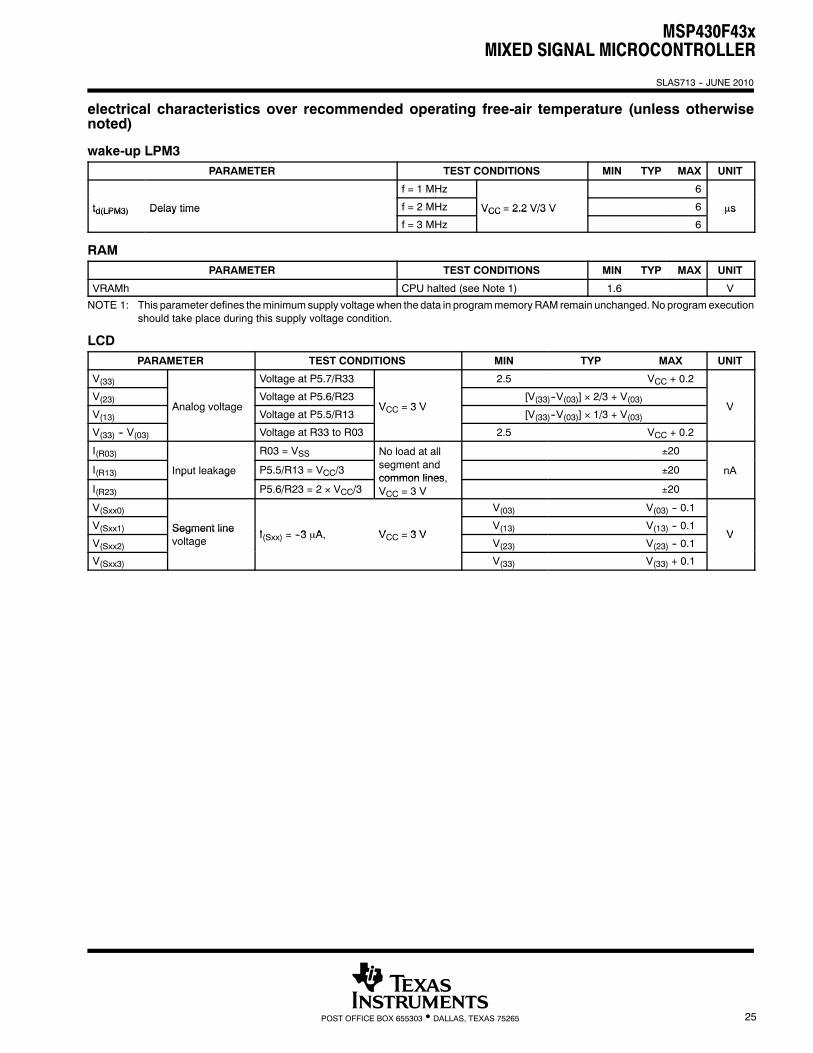
wake-up LPM3PARAMETER TEST CONDITIONS MIN TYP MAX UNIT
f = 1 MHz 6
td(LPM3) Delay time f = 2 MHz VCC = 2.2 V/3 V 6 µstd(LPM3) Delay time
f = 3 MHz
VCC 2.2 V/3 V
6
µs
RAMPARAMETER TEST CONDITIONS MIN TYP MAX UNIT
VRAMh CPU halted (see Note 1) 1.6 V
NOTE 1: This parameter defines theminimumsupply voltagewhen the data in programmemoryRAM remain unchanged. No programexecutionshould take place during this supply voltage condition.
LCDPARAMETER TEST CONDITIONS MIN TYP MAX UNIT
V(33) Voltage at P5.7/R33 2.5 VCC + 0.2
V(23)Analog oltage
Voltage at P5.6/R23V 3 V
[V(33)--V(03)] × 2/3 + V(03)V
V(13)Analog voltage
Voltage at P5.5/R13VCC = 3 V [V(33)--V(03)] × 1/3 + V(03)
V
V(33) -- V(03) Voltage at R33 to R03 2.5 VCC + 0.2
I(R03) R03 = VSS No load at all ±20
I(R13) Input leakage P5.5/R13 = VCC/3segment andcommon lines
±20 nA
I(R23)
p g
P5.6/R23 = 2 × VCC/3common lines,VCC = 3 V ±20
V(Sxx0) V(03) V(03) -- 0.1
V(Sxx1) Segment line I 3 µA V 3 VV(13) V(13) -- 0.1
VV(Sxx2)
Segment linevoltage
I(Sxx) = --3 µA, VCC = 3 VV(23) V(23) -- 0.1
V
V(Sxx3) V(33) V(33) + 0.1
MSP430F43xMIXED SIGNAL MICROCONTROLLER
SLAS713 -- JUNE 2010
26 POST OFFICE BOX 655303 • DALLAS, TEXAS 75265
electrical characteristics over recommended operating free-air temperature (unless otherwisenoted) (continued)
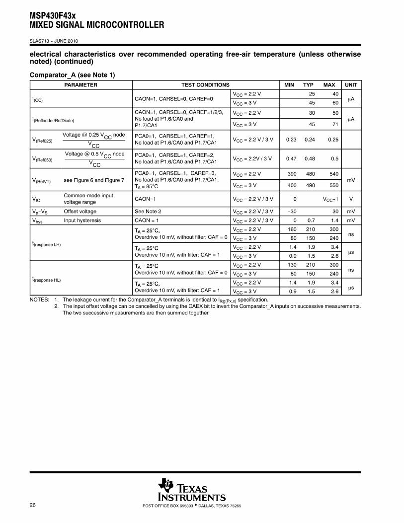
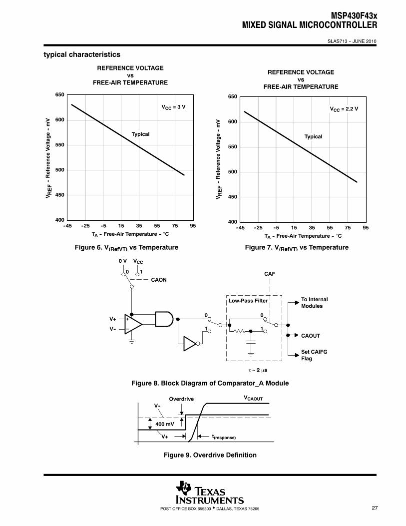
Comparator_A (see Note 1)PARAMETER TEST CONDITIONS MIN TYP MAX UNIT
I CAON 1 CARSEL 0 CAREF 0VCC = 2.2 V 25 40
AI(CC) CAON=1, CARSEL=0, CAREF=0VCC = 3 V 45 60
µA
ICAON=1, CARSEL=0, CAREF=1/2/3,No load at P1 6/CA0 and
VCC = 2.2 V 30 50AI(Refladder/RefDiode) No load at P1.6/CA0 and
P1.7/CA1 VCC = 3 V 45 71µA
V(Ref025)Voltage @ 0.25 VCC node
VCC
PCA0=1, CARSEL=1, CAREF=1,No load at P1.6/CA0 and P1.7/CA1 VCC = 2.2 V / 3 V 0.23 0.24 0.25
V(Ref050)Voltage @ 0.5 VCC node
VCC
PCA0=1, CARSEL=1, CAREF=2,No load at P1.6/CA0 and P1.7/CA1 VCC = 2.2V / 3 V 0.47 0.48 0.5
V see Figure 6 and Figure 7PCA0=1, CARSEL=1, CAREF=3,No load at P1 6/CA0 and P1 7/CA1;
VCC = 2.2 V 390 480 540mVV(RefVT) see Figure 6 and Figure 7 No load at P1.6/CA0 and P1.7/CA1;
TA = 85°C VCC = 3 V 400 490 550mV
VICCommon-mode inputvoltage range CAON=1 VCC = 2.2 V / 3 V 0 VCC--1 V
Vp--VS Offset voltage See Note 2 VCC = 2.2 V / 3 V --30 30 mV
Vhys Input hysteresis CAON = 1 VCC = 2.2 V / 3 V 0 0.7 1.4 mV
TA = 25°C, VCC = 2.2 V 160 210 300ns
t
TA = 25 C,Overdrive 10 mV, without filter: CAF = 0 VCC = 3 V 80 150 240
ns
t(response LH)TA = 25°C VCC = 2.2 V 1.4 1.9 3.4
sTA = 25 COverdrive 10 mV, with filter: CAF = 1 VCC = 3 V 0.9 1.5 2.6
µs
TA = 25°C VCC = 2.2 V 130 210 300ns
t
TA = 25 COverdrive 10 mV, without filter: CAF = 0 VCC = 3 V 80 150 240
ns
t(response HL)TA = 25°C, VCC = 2.2 V 1.4 1.9 3.4
sTA = 25 C,Overdrive 10 mV, with filter: CAF = 1 VCC = 3 V 0.9 1.5 2.6
µs
NOTES: 1. The leakage current for the Comparator_A terminals is identical to Ilkg(Px.x) specification.2. The input offset voltage can be cancelled by using the CAEX bit to invert the Comparator_A inputs on successive measurements.
The two successive measurements are then summed together.
MSP430F43xMIXED SIGNAL MICROCONTROLLER
SLAS713 -- JUNE 2010
27POST OFFICE BOX 655303 • DALLAS, TEXAS 75265
typical characteristics
TA -- Free-Air Temperature -- °C
400
450
500
550
600
650
--45 --25 --5 15 35 55 75 95
VCC = 3 V
Figure 6. V(RefVT) vs Temperature
V REF--Reference
Voltage--mV
Typical
REFERENCE VOLTAGEvs
FREE-AIR TEMPERATURE
Figure 7. V(RefVT) vs Temperature
TA -- Free-Air Temperature -- °C
400
450
500
550
600
650
--45 --25 --5 15 35 55 75 95
VCC = 2.2 V
Typical
REFERENCE VOLTAGEvs
FREE-AIR TEMPERATURE
V REF--Reference
Voltage--mV
_+
CAON
0
1
V+0
1
CAF
Low-Pass Filter
τ ≈ 2 µs
To InternalModules
Set CAIFGFlag
CAOUTV--
VCC
1
0 V
0
Figure 8. Block Diagram of Comparator_A Module
Overdrive VCAOUT
t(response)V+
V--
400 mV
Figure 9. Overdrive Definition
MSP430F43xMIXED SIGNAL MICROCONTROLLER
SLAS713 -- JUNE 2010
28 POST OFFICE BOX 655303 • DALLAS, TEXAS 75265
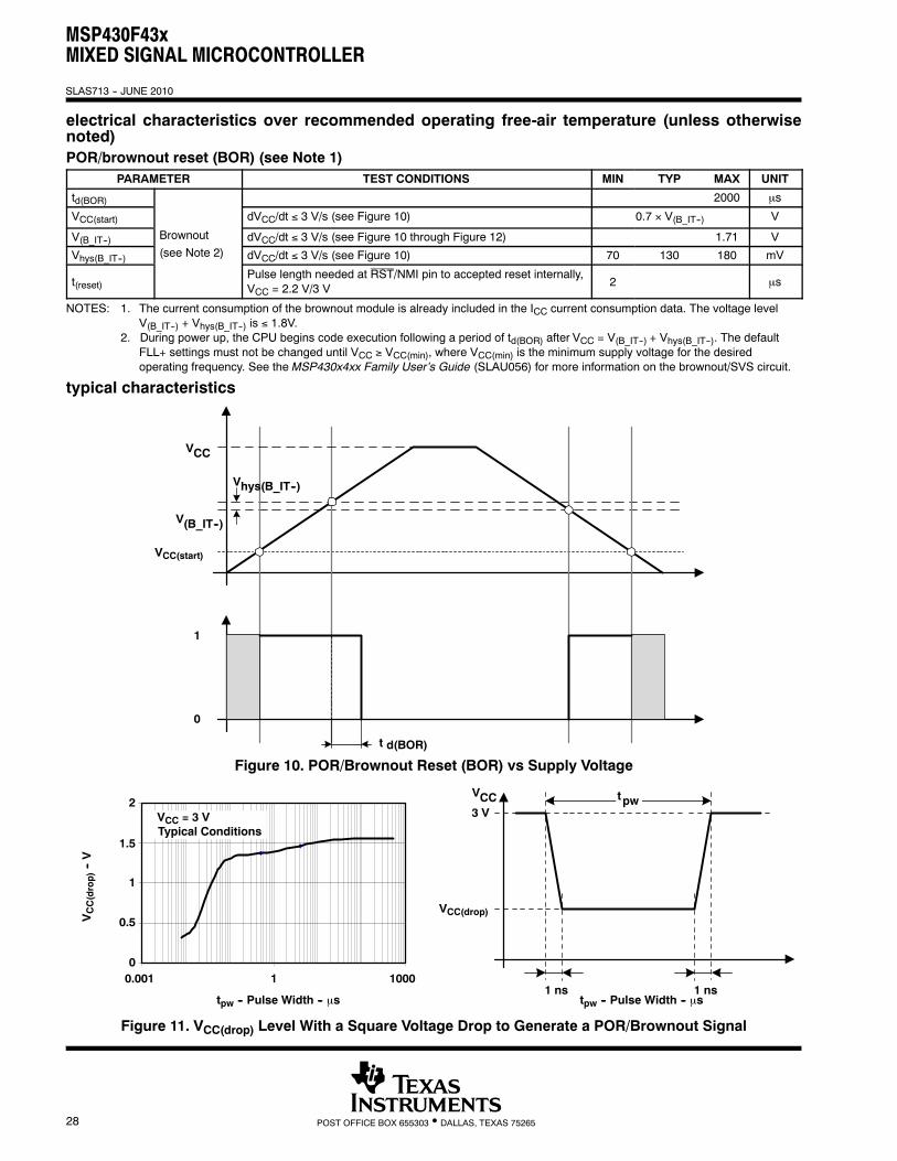
electrical characteristics over recommended operating free-air temperature (unless otherwisenoted)POR/brownout reset (BOR) (see Note 1)
PARAMETER TEST CONDITIONS MIN TYP MAX UNIT
td(BOR) 2000 µs
VCC(start) dVCC/dt ≤ 3 V/s (see Figure 10) 0.7 × V(B_IT--) V
V(B_IT--) Brownout dVCC/dt ≤ 3 V/s (see Figure 10 through Figure 12) 1.71 V
Vhys(B_IT--) (see Note 2) dVCC/dt ≤ 3 V/s (see Figure 10) 70 130 180 mV
t(reset)Pulse length needed at RST/NMI pin to accepted reset internally,VCC = 2.2 V/3 V
2 µs
NOTES: 1. The current consumption of the brownout module is already included in the ICC current consumption data. The voltage levelV(B_IT--) + Vhys(B_IT--) is ≤ 1.8V.
2. During power up, the CPU begins code execution following a period of td(BOR) after VCC = V(B_IT--) + Vhys(B_IT--). The defaultFLL+ settings must not be changed until VCC ≥ VCC(min), where VCC(min) is the minimum supply voltage for the desiredoperating frequency. See the MSP430x4xx Family User’s Guide (SLAU056) for more information on the brownout/SVS circuit.
typical characteristics
0
1
t d(BOR)
VCC
V(B_IT--)
Vhys(B_IT--)
VCC(start)
Figure 10. POR/Brownout Reset (BOR) vs Supply Voltage
VCC3 V
tpw
0
0.5
1
1.5
2
0.001 1 1000
Typical Conditions
1 ns 1 nstpw -- Pulse Width -- µs tpw -- Pulse Width -- µs
VCC = 3 V
VCC(drop)--V
VCC(drop)
Figure 11. VCC(drop) Level With a Square Voltage Drop to Generate a POR/Brownout Signal
MSP430F43xMIXED SIGNAL MICROCONTROLLER
SLAS713 -- JUNE 2010
29POST OFFICE BOX 655303 • DALLAS, TEXAS 75265
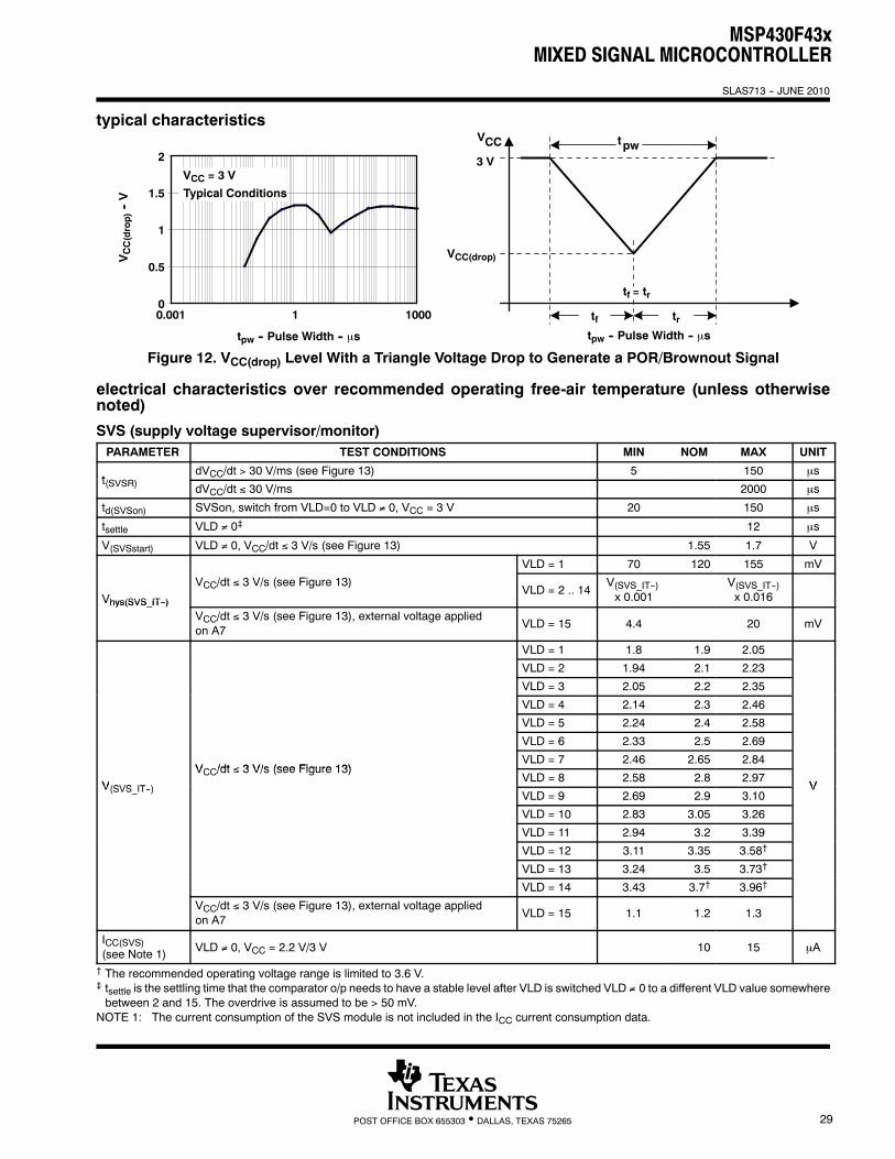
typical characteristicsVCC
0
0.5
1
1.5
2tpw
tpw -- Pulse Width -- µs
3 V
0.001 1 1000 tf trtpw -- Pulse Width -- µs
tf = tr
Typical Conditions
VCC = 3 V
VCC(drop)--V
VCC(drop)
Figure 12. VCC(drop) Level With a Triangle Voltage Drop to Generate a POR/Brownout Signal
electrical characteristics over recommended operating free-air temperature (unless otherwisenoted)
SVS (supply voltage supervisor/monitor)PARAMETER TEST CONDITIONS MIN NOM MAX UNIT
tdVCC/dt > 30 V/ms (see Figure 13) 5 150 µs
t(SVSR) dVCC/dt ≤ 30 V/ms 2000 µs
td(SVSon) SVSon, switch from VLD=0 to VLD ≠ 0, VCC = 3 V 20 150 µs
tsettle VLD ≠ 0‡ 12 µs
V(SVSstart) VLD ≠ 0, VCC/dt ≤ 3 V/s (see Figure 13) 1.55 1.7 V
VLD = 1 70 120 155 mV
Vhys(SVS IT--)
VCC/dt ≤ 3 V/s (see Figure 13) VLD = 2 .. 14V(SVS_IT--)x 0.001
V(SVS_IT--)x 0.016Vhys(SVS_IT--)
VCC/dt ≤ 3 V/s (see Figure 13), external voltage appliedon A7 VLD = 15 4.4 20 mV
VLD = 1 1.8 1.9 2.05
VLD = 2 1.94 2.1 2.23
VLD = 3 2.05 2.2 2.35
VLD = 4 2.14 2.3 2.46
VLD = 5 2.24 2.4 2.58
VLD = 6 2.33 2.5 2.69
V /dt ≤ 3 V/s (see Figure 13)VLD = 7 2.46 2.65 2.84
V(SVS IT )
VCC/dt ≤ 3 V/s (see Figure 13) VLD = 8 2.58 2.8 2.97VV(SVS_IT--)
VLD = 9 2.69 2.9 3.10V
VLD = 10 2.83 3.05 3.26
VLD = 11 2.94 3.2 3.39
VLD = 12 3.11 3.35 3.58†
VLD = 13 3.24 3.5 3.73†
VLD = 14 3.43 3.7† 3.96†
VCC/dt ≤ 3 V/s (see Figure 13), external voltage appliedon A7 VLD = 15 1.1 1.2 1.3
ICC(SVS)(see Note 1) VLD ≠ 0, VCC = 2.2 V/3 V 10 15 µA
† The recommended operating voltage range is limited to 3.6 V.‡ tsettle is the settling time that the comparator o/p needs to have a stable level after VLD is switched VLD ≠ 0 to a different VLD value somewherebetween 2 and 15. The overdrive is assumed to be > 50 mV.
NOTE 1: The current consumption of the SVS module is not included in the ICC current consumption data.
MSP430F43xMIXED SIGNAL MICROCONTROLLER
SLAS713 -- JUNE 2010
30 POST OFFICE BOX 655303 • DALLAS, TEXAS 75265
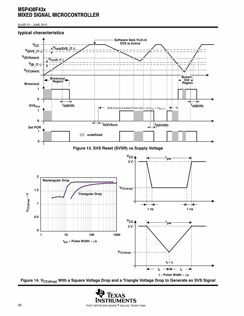
typical characteristics
VCC(start)
VCC
V(B_IT--)
BrownoutRegion
V(SVSstart)
V(SVS_IT--)
Software Sets VLD>0:SVS is Active
td(SVSR)
undefined
Vhys(SVS_IT--)
0
1
td(BOR)
Brownout
0
1
td(SVSon)
td(BOR)
0
1Set POR
Brown-OutRegion
SVS Circuit is Active From VLD > to VCC < V(B_IT--)SVSOut
Vhys(B_IT--)
Figure 13. SVS Reset (SVSR) vs Supply Voltage
0
0.5
1
1.5
2
VCC
VCC
1 ns 1 ns
tpw
tpw -- Pulse Width -- µs
3 V
1 10 1000
tf tr
t -- Pulse Width -- µs
100
tpw3 V
tf = tr
Rectangular Drop
Triangular Drop
VCC(drop)--V
VCC(drop)
VCC(drop)
Figure 14. VCC(drop) With a Square Voltage Drop and a Triangle Voltage Drop to Generate an SVS Signal
MSP430F43xMIXED SIGNAL MICROCONTROLLER
SLAS713 -- JUNE 2010
31POST OFFICE BOX 655303 • DALLAS, TEXAS 75265
electrical characteristics over recommended operating free-air temperature (unless otherwisenoted)
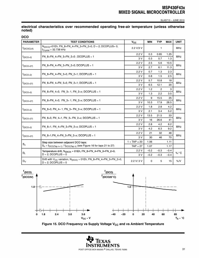
DCOPARAMETER TEST CONDITIONS VCC MIN TYP MAX UNIT
f(DCOCLK)N(DCO)=01Eh, FN_8=FN_4=FN_3=FN_2=0, D = 2; DCOPLUS= 0,fCrystal = 32.738 kHz
2.2 V/3 V 1 MHz
f FN 8 FN 4 FN 3 FN 2 0 DCOPLUS 12.2 V 0.3 0.65 1.25
MHf(DCO=2) FN_8=FN_4=FN_3=FN_2=0 ; DCOPLUS = 13 V 0.3 0.7 1.3
MHz
f FN 8 FN 4 FN 3 FN 2 0 DCOPLUS 12.2 V 2.5 5.6 10.5
MHf(DCO=27) FN_8=FN_4=FN_3=FN_2=0; DCOPLUS = 13 V 2.7 6.1 11.3
MHz
f FN 8 FN 4 FN 3 0 FN 2 1 DCOPLUS 12.2 V 0.7 1.3 2.3
MHf(DCO=2) FN_8=FN_4=FN_3=0, FN_2=1; DCOPLUS = 13 V 0.8 1.5 2.5
MHz
f FN 8 FN 4 FN 3 0 FN 2 1 DCOPLUS 12.2 V 5.7 10.8 18
MHf(DCO=27) FN_8=FN_4=FN_3=0, FN_2=1; DCOPLUS = 13 V 6.5 12.1 20
MHz
f FN 8 FN 4 0 FN 3 1 FN 2 DCOPLUS 12.2 V 1.2 2 3
MHf(DCO=2) FN_8=FN_4=0, FN_3= 1, FN_2=x; DCOPLUS = 13 V 1.3 2.2 3.5
MHz
f FN 8 FN 4 0 FN 3 1 FN 2 DCOPLUS 12.2 V 9 15.5 25
MHf(DCO=27) FN_8=FN_4=0, FN_3= 1, FN_2=x; DCOPLUS = 13 V 10.3 17.9 28.5
MHz
f FN 8 0 FN 4 1 FN 3 FN 2 DCOPLUS 12.2 V 1.8 2.8 4.2
MHf(DCO=2) FN_8=0, FN_4= 1, FN_3= FN_2=x; DCOPLUS = 13 V 2.1 3.4 5.2
MHz
f FN 8 0 FN 4 1 FN 3 FN 2 DCOPLUS 12.2 V 13.5 21.5 33
MHf(DCO=27) FN_8=0, FN_4=1, FN_3= FN_2=x; DCOPLUS = 13 V 16 26.6 41
MHz
f FN 8 1 FN 4 FN 3 FN 2 DCOPLUS 12.2 V 2.8 4.2 6.2
MHf(DCO=2) FN_8=1, FN_4=FN_3=FN_2=x; DCOPLUS = 13 V 4.2 6.3 9.2
MHz
f FN 8 1 FN 4 FN 3 FN 2 DCOPLUS 12.2 V 21 32 46
MHf(DCO=27) FN_8=1,FN_4=FN_3=FN_2=x; DCOPLUS = 13 V 30 46 70
MHz
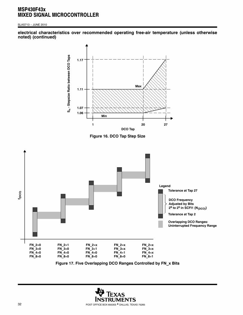
SStep size between adjacent DCO taps: 1 < TAP ≤ 20 1.06 1.11
SnStep size between adjacent DCO taps:Sn = fDCO(Tap n+1) / fDCO(Tap n) (see Figure 16 for taps 21 to 27) TAP = 27 1.07 1.17
DTemperature drift, N(DCO) = 01Eh, FN_8=FN_4=FN_3=FN_2=0, 2.2 V –0.2 –0.3 –0.4
%/_CDtTemperature drift, N(DCO) = 01Eh, FN_8=FN_4=FN_3=FN_2=0,D = 2; DCOPLUS = 0 3 V –0.2 –0.3 –0.4
%/_C
DVDrift with VCC variation, N(DCO) = 01Eh, FN_8=FN_4=FN_3=FN_2=0,D = 2; DCOPLUS = 0 2.2 V/ 3 V 0 5 15 %/V
TA -- °CVCC -- V
f(DCO)f(DCO20°C)
f(DCO)f(DCO3V)
1.8 3.02.4 3.6
1.0
20 6040 85
1.0
0--20--400
Figure 15. DCO Frequency vs Supply Voltage VCC and vs Ambient Temperature
MSP430F43xMIXED SIGNAL MICROCONTROLLER
SLAS713 -- JUNE 2010
32 POST OFFICE BOX 655303 • DALLAS, TEXAS 75265
electrical characteristics over recommended operating free-air temperature (unless otherwisenoted) (continued)
1 2720
1.11
1.17
DCO Tap
Sn-S
tepsize
RatiobetweenDCOTaps
Min
Max
1.07
1.06
Figure 16. DCO Tap Step Size
DCO FrequencyAdjusted by Bits29 to 25 in SCFI1 NDCO
FN_2=0FN_3=0FN_4=0FN_8=0
FN_2=1FN_3=0FN_4=0FN_8=0
FN_2=xFN_3=1FN_4=0FN_8=0
FN_2=xFN_3=xFN_4=1FN_8=0
FN_2=xFN_3=xFN_4=xFN_8=1
LegendTolerance at Tap 27
Tolerance at Tap 2
Overlapping DCO Ranges:Uninterrupted Frequency Range
f (DCO)
Figure 17. Five Overlapping DCO Ranges Controlled by FN_x Bits
MSP430F43xMIXED SIGNAL MICROCONTROLLER
SLAS713 -- JUNE 2010
33POST OFFICE BOX 655303 • DALLAS, TEXAS 75265
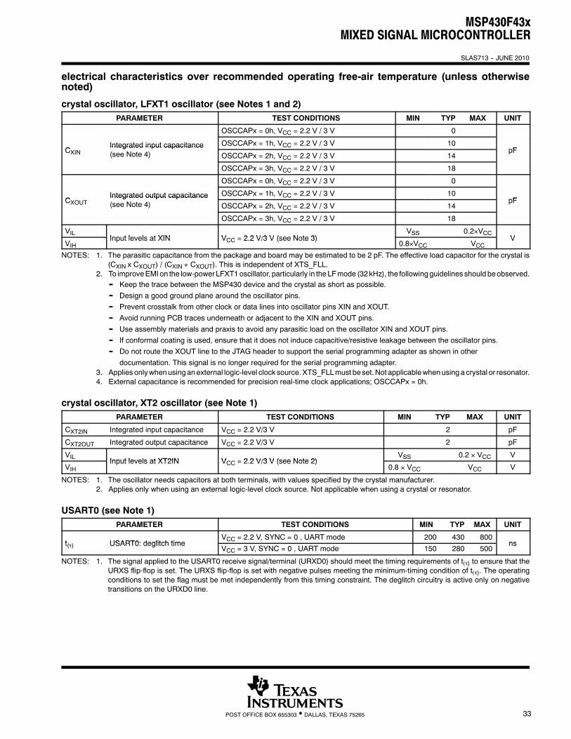
electrical characteristics over recommended operating free-air temperature (unless otherwisenoted)
crystal oscillator, LFXT1 oscillator (see Notes 1 and 2)PARAMETER TEST CONDITIONS MIN TYP MAX UNIT
OSCCAPx = 0h, VCC = 2.2 V / 3 V 0
CIntegrated input capacitance OSCCAPx = 1h, VCC = 2.2 V / 3 V 10
pFCXINIntegrated input capacitance(see Note 4) OSCCAPx = 2h, VCC = 2.2 V / 3 V 14
pF
OSCCAPx = 3h, VCC = 2.2 V / 3 V 18
OSCCAPx = 0h, VCC = 2.2 V / 3 V 0
CIntegrated output capacitance OSCCAPx = 1h, VCC = 2.2 V / 3 V 10
pFCXOUTIntegrated output capacitance(see Note 4) OSCCAPx = 2h, VCC = 2.2 V / 3 V 14
pF
OSCCAPx = 3h, VCC = 2.2 V / 3 V 18
VILInput levels at XIN V 2 2 V/3 V (see Note 3)
VSS 0.2×VCCV
VIHInput levels at XIN VCC = 2.2 V/3 V (see Note 3)
0.8×VCC VCCV
NOTES: 1. The parasitic capacitance from the package and board may be estimated to be 2 pF. The effective load capacitor for the crystal is(CXIN x CXOUT) / (CXIN + CXOUT). This is independent of XTS_FLL.
2. To improveEMIon the low-powerLFXT1oscillator, particularly in theLFmode (32kHz), the followingguidelines should beobserved.-- Keep the trace between the MSP430 device and the crystal as short as possible.-- Design a good ground plane around the oscillator pins.-- Prevent crosstalk from other clock or data lines into oscillator pins XIN and XOUT.-- Avoid running PCB traces underneath or adjacent to the XIN and XOUT pins.-- Use assembly materials and praxis to avoid any parasitic load on the oscillator XIN and XOUT pins.-- If conformal coating is used, ensure that it does not induce capacitive/resistive leakage between the oscillator pins.-- Do not route the XOUT line to the JTAG header to support the serial programming adapter as shown in other
documentation. This signal is no longer required for the serial programming adapter.3. Applies onlywhenusinganexternal logic-level clock source.XTS_FLLmust beset.Not applicablewhenusingacrystal or resonator.4. External capacitance is recommended for precision real-time clock applications; OSCCAPx = 0h.
crystal oscillator, XT2 oscillator (see Note 1)PARAMETER TEST CONDITIONS MIN TYP MAX UNIT
CXT2IN Integrated input capacitance VCC = 2.2 V/3 V 2 pF
CXT2OUT Integrated output capacitance VCC = 2.2 V/3 V 2 pF
VILInput levels at XT2IN V 2 2 V/3 V (see Note 2)
VSS 0.2 × VCC V
VIHInput levels at XT2IN VCC = 2.2 V/3 V (see Note 2)
0.8 × VCC VCC V
NOTES: 1. The oscillator needs capacitors at both terminals, with values specified by the crystal manufacturer.2. Applies only when using an external logic-level clock source. Not applicable when using a crystal or resonator.
USART0 (see Note 1)PARAMETER TEST CONDITIONS MIN TYP MAX UNIT
t USART0: deglitch timeVCC = 2.2 V, SYNC = 0 , UART mode 200 430 800
nst(τ) USART0: deglitch timeVCC = 3 V, SYNC = 0 , UART mode 150 280 500
ns
NOTES: 1. The signal applied to the USART0 receive signal/terminal (URXD0) should meet the timing requirements of t(τ) to ensure that theURXS flip-flop is set. The URXS flip-flop is set with negative pulses meeting the minimum-timing condition of t(τ). The operatingconditions to set the flag must be met independently from this timing constraint. The deglitch circuitry is active only on negativetransitions on the URXD0 line.
MSP430F43xMIXED SIGNAL MICROCONTROLLER
SLAS713 -- JUNE 2010
34 POST OFFICE BOX 655303 • DALLAS, TEXAS 75265
electrical characteristics over recommended operating free-air temperature (unless otherwisenoted) (continued)
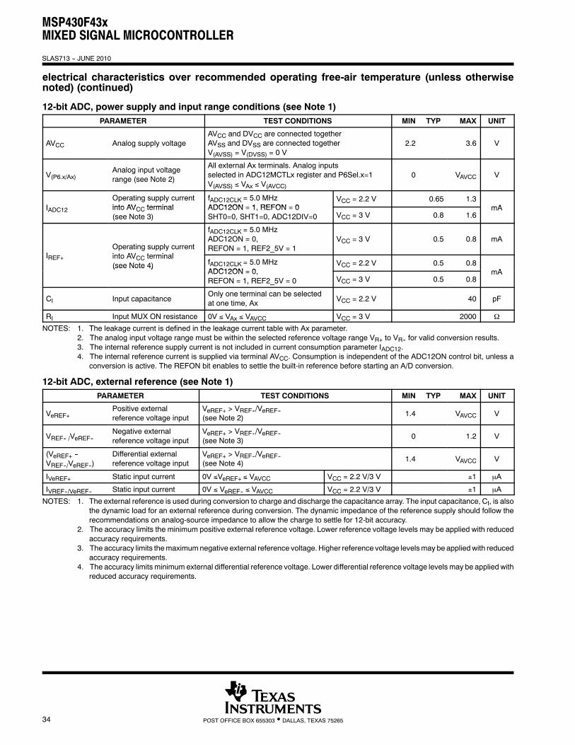
12-bit ADC, power supply and input range conditions (see Note 1)PARAMETER TEST CONDITIONS MIN TYP MAX UNIT
AVCC Analog supply voltageAVCC and DVCC are connected togetherAVSS and DVSS are connected togetherV(AVSS) = V(DVSS) = 0 V
2.2 3.6 V
V(P6.x/Ax)Analog input voltagerange (see Note 2)
All external Ax terminals. Analog inputsselected in ADC12MCTLx register and P6Sel.x=1V(AVSS) ≤ VAx ≤ V(AVCC)
0 VAVCC V
IOperating supply currentinto AV terminal
fADC12CLK = 5.0 MHzADC12ON 1 REFON 0
VCC = 2.2 V 0.65 1.3mAIADC12 into AVCC terminal
(see Note 3)ADC12ON = 1, REFON = 0SHT0=0, SHT1=0, ADC12DIV=0 VCC = 3 V 0.8 1.6
mA
IOperating supply currenti t AV t i l
fADC12CLK = 5.0 MHzADC12ON = 0,REFON = 1, REF2_5V = 1
VCC = 3 V 0.5 0.8 mA
IREF+ into AVCC terminal(see Note 4) fADC12CLK = 5.0 MHz
ADC12ON 0VCC = 2.2 V 0.5 0.8
mA(see Note 4)
ADC12ON = 0,REFON = 1, REF2_5V = 0 VCC = 3 V 0.5 0.8
mA
CI Input capacitanceOnly one terminal can be selectedat one time, Ax VCC = 2.2 V 40 pF
RI Input MUX ON resistance 0V ≤ VAx ≤ VAVCC VCC = 3 V 2000 Ω
NOTES: 1. The leakage current is defined in the leakage current table with Ax parameter.2. The analog input voltage range must be within the selected reference voltage range VR+ to VR-- for valid conversion results.3. The internal reference supply current is not included in current consumption parameter IADC12.4. The internal reference current is supplied via terminal AVCC. Consumption is independent of the ADC12ON control bit, unless a
conversion is active. The REFON bit enables to settle the built-in reference before starting an A/D conversion.
12-bit ADC, external reference (see Note 1)PARAMETER TEST CONDITIONS MIN TYP MAX UNIT
VeREF+Positive externalreference voltage input
VeREF+ > VREF--/VeREF--(see Note 2) 1.4 VAVCC V
VREF-- /VeREF--Negative externalreference voltage input
VeREF+ > VREF--/VeREF--(see Note 3) 0 1.2 V
(VeREF+ --VREF--/VeREF--)
Differential externalreference voltage input
VeREF+ > VREF--/VeREF--(see Note 4) 1.4 VAVCC V
IVeREF+ Static input current 0V ≤VeREF+ ≤ VAVCC VCC = 2.2 V/3 V ±1 µA
IVREF--/VeREF-- Static input current 0V ≤ VeREF-- ≤ VAVCC VCC = 2.2 V/3 V ±1 µA
NOTES: 1. The external reference is used during conversion to charge and discharge the capacitance array. The input capacitance, CI, is alsothe dynamic load for an external reference during conversion. The dynamic impedance of the reference supply should follow therecommendations on analog-source impedance to allow the charge to settle for 12-bit accuracy.
2. The accuracy limits the minimum positive external reference voltage. Lower reference voltage levels may be applied with reducedaccuracy requirements.
3. The accuracy limits themaximumnegative external reference voltage. Higher reference voltage levelsmay be appliedwith reducedaccuracy requirements.
4. The accuracy limits minimum external differential reference voltage. Lower differential reference voltage levels may be applied withreduced accuracy requirements.
MSP430F43xMIXED SIGNAL MICROCONTROLLER
SLAS713 -- JUNE 2010
35POST OFFICE BOX 655303 • DALLAS, TEXAS 75265
electrical characteristics over recommended operating free-air temperature (unless otherwisenoted) (continued)
12-bit ADC, built-in referencePARAMETER TEST CONDITIONS MIN TYP MAX UNIT
VPositive built-in reference
REF2_5V = 1 for 2.5 VIVREF+max ≤ IVREF+≤ IVREF+min
VCC = 3 V 2.4 2.5 2.6
VVREF+Positive built in referencevoltage output REF2_5V = 0 for 1.5 V
IVREF+max ≤ IVREF+≤ IVREF+minVCC = 2.2 V/3 V 1.44 1.5 1.56
V
AVCC minimum voltage, REF2_5V = 0, IVREF+max ≤ IVREF+≤ IVREF+min 2.2
AVCC(min)
AVCC minimum voltage,Positive built-in reference REF2_5V = 1, IVREF+min ≥ IVREF+≥ --0.5mA 2.8 VAVCC(min) Positive built in referenceactive REF2_5V = 1, IVREF+min ≥ IVREF+≥ --1mA 2.9
V
ILoad current out of VREF+ VCC = 2.2 V 0.01 --0.5
mAIVREF+Load current out of VREF+terminal VCC = 3 V 0.01 --1
mA
IVREF+ = 500 µA +/-- 100 µAAnalog input voltage 0 75 V;
VCC = 2.2 V ±2LSB
ILoad-current regulation
Analog input voltage ~0.75 V;REF2_5V = 0 VCC = 3 V ±2
LSB
IL(VREF)+Load current regulationVREF+ terminal IVREF+ = 500 µA ± 100 µA
Analog input voltage ~1.25 V;REF2_5V = 1
VCC = 3 V ±2 LSB
ILoad current regulation IVREF+ =100 µA→ 900 µA,
C 5 F ax 0 5 x V V 3 V 20 nsIDL(VREF) +Load current regulationVREF+ terminal
CVREF+=5 µF, ax ~0.5 x VREF+Error of conversion result ≤ 1 LSB
VCC = 3 V 20 ns
CVREF+Capacitance at pin VREF+(see Note 1)
REFON =1,0 mA ≤ IVREF+ ≤ IVREF+max
VCC = 2.2 V/3 V 5 10 µF
TREF+Temperature coefficient ofbuilt-in reference
IVREF+ is a constant in the range of0 mA ≤ IVREF+ ≤ 1 mA
VCC = 2.2 V/3 V ±100 ppm/°C
tREFONSettle time of internalreference voltage (seeFigure 18 and Note 2)
IVREF+ = 0.5 mA, CVREF+ = 10 µF,VREF+ = 1.5 V, VAVCC = 2.2 V
17 ms
NOTES: 1. The internal buffer operational amplifier and the accuracy specifications require an external capacitor. All INL and DNL tests usestwo capacitors between pins VREF+ and AVSS and VREF--/VeREF-- and AVSS: 10 µF tantalum and 100 nF ceramic.
2. The condition is that the error in a conversion started after tREFON is less than ±0.5 LSB. The settling time depends on the externalcapacitive load.
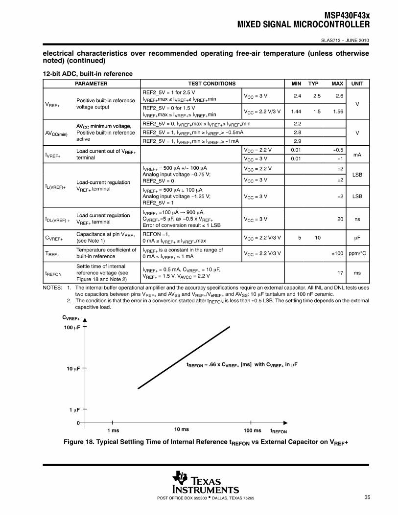
CVREF+
1 µF
01 ms 10 ms 100 ms tREFON
tREFON ≈ .66 x CVREF+ [ms] with CVREF+ in µF
100 µF
10 µF
Figure 18. Typical Settling Time of Internal Reference tREFON vs External Capacitor on VREF+
MSP430F43xMIXED SIGNAL MICROCONTROLLER
SLAS713 -- JUNE 2010
36 POST OFFICE BOX 655303 • DALLAS, TEXAS 75265
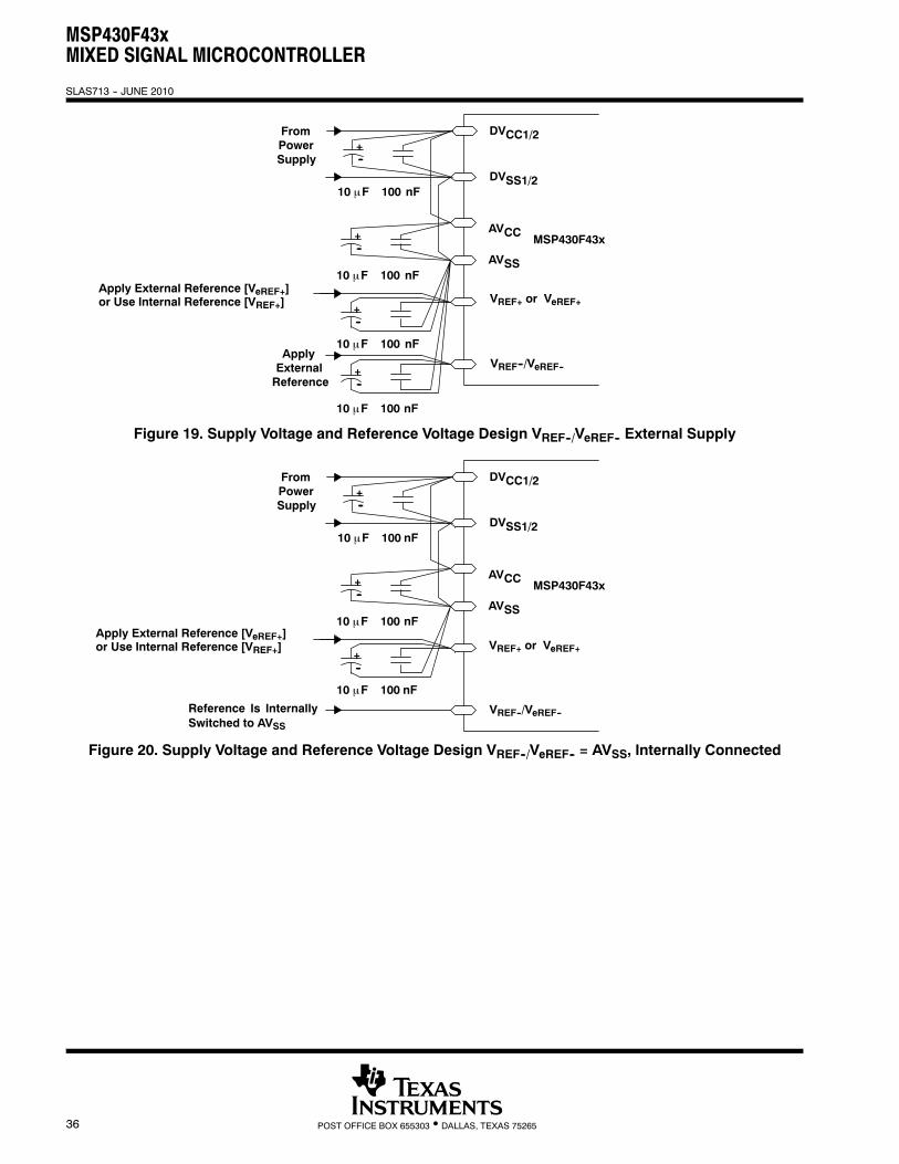
+--
10 µF 100 nFAVSS
MSP430F43x
+--
+--
10 µF 100 nF
10 µF 100 nF
AVCC
10 µF 100 nFDVSS1/2
DVCC1/2FromPowerSupply
ApplyExternalReference
+--
Apply External Reference [VeREF+]or Use Internal Reference [VREF+] VREF+ or VeREF+
VREF--/VeREF--
Figure 19. Supply Voltage and Reference Voltage Design VREF--/VeREF-- External Supply
+--
10 µF 100 nFAVSS
MSP430F43x
+--
10 µF 100 nF
AVCC
10 µF 100 nFDVSS1/2
DVCC1/2FromPowerSupply
+--
Apply External Reference [VeREF+]or Use Internal Reference [VREF+] VREF+ or VeREF+
VREF--/VeREF--Reference Is InternallySwitched to AVSS
Figure 20. Supply Voltage and Reference Voltage Design VREF--/VeREF-- = AVSS, Internally Connected
MSP430F43xMIXED SIGNAL MICROCONTROLLER
SLAS713 -- JUNE 2010
37POST OFFICE BOX 655303 • DALLAS, TEXAS 75265
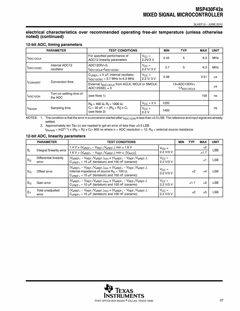
electrical characteristics over recommended operating free-air temperature (unless otherwisenoted) (continued)
12-bit ADC, timing parametersPARAMETER TEST CONDITIONS MIN TYP MAX UNIT
fADC12CLKFor specified performance ofADC12 linearity parameters
VCC =2.2V/3 V 0.45 5 6.3 MHz
fADC12OSCInternal ADC12oscillator
ADC12DIV=0,fADC12CLK=fADC12OSC
VCC =2.2 V/ 3 V 3.7 5 6.3 MHz
t Conversion time
CVREF+ ≥ 5 µF, Internal oscillator,fADC12OSC = 3.7 MHz to 6.3 MHz
VCC =2.2 V/ 3 V 2.06 3.51 µs
tCONVERT Conversion timeExternal fADC12CLK from ACLK, MCLK or SMCLK:ADC12SSEL ≠ 0
13×ADC12DIV×1/fADC12CLK
µs
tADC12ONTurn on settling time ofthe ADC (see Note 1) 100 ns
RS = 400 Ω, RI = 1000 Ω, VCC = 3 V 1220
tSample Sampling timeRS = 400 Ω, RI = 1000 Ω,CI = 30 pF, τ = [RS + RI] x CI(see Note 2)
VCC =2.2 V 1400
ns
NOTES: 1. The condition is that the error in a conversion started after tADC12ON is less than ±0.5 LSB. The reference and input signal are alreadysettled.
2. Approximately ten Tau (τ) are needed to get an error of less than ±0.5 LSB:tSample = ln(2n+1) x (RS + RI) x CI+ 800 ns where n = ADC resolution = 12, RS = external source resistance.
12-bit ADC, linearity parametersPARAMETER TEST CONDITIONS MIN TYP MAX UNIT
E Integral linearity error1.4 V ≤ (VeREF+ -- VREF--/VeREF--) min ≤ 1.6 V VCC = ±2
LSBEI Integral linearity error1.6 V < (VeREF+ -- VREF--/VeREF--) min ≤ [VAVCC]
VCC =2.2 V/3 V ±1.7
LSB
EDDifferential linearityerror
(VeREF+ -- VREF--/VeREF--)min ≤ (VeREF+ -- VREF--/VeREF--),CVREF+ = 10 µF (tantalum) and 100 nF (ceramic)
VCC =2.2 V/3 V ±1 LSB
EO Offset error(VeREF+ -- VREF--/VeREF--)min ≤ (VeREF+ -- VREF--/VeREF--),Internal impedance of source RS < 100 Ω,CVREF+ = 10 µF (tantalum) and 100 nF (ceramic)
VCC =2.2 V/3 V ±2 ±4 LSB
EG Gain error(VeREF+ -- VREF--/VeREF--)min ≤ (VeREF+ -- VREF--/VeREF--),CVREF+ = 10 µF (tantalum) and 100 nF (ceramic)
VCC =2.2 V/3 V ±1.1 ±2 LSB
ETTotal unadjustederror
(VeREF+ -- VREF--/VeREF--)min ≤ (VeREF+ -- VREF--/VeREF--),CVREF+ = 10 µF (tantalum) and 100 nF (ceramic)
VCC =2.2 V/3 V ±2 ±5 LSB
MSP430F43xMIXED SIGNAL MICROCONTROLLER
SLAS713 -- JUNE 2010
38 POST OFFICE BOX 655303 • DALLAS, TEXAS 75265
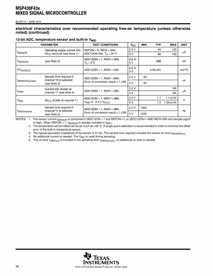
electrical characteristics over recommended operating free-air temperature (unless otherwisenoted) (continued)
12-bit ADC, temperature sensor and built-in VMIDPARAMETER TEST CONDITIONS VCC MIN TYP MAX UNIT
IOperating supply current into REFON = 0, INCH = 0Ah, 2.2 V 40 120
AISENSOROperating supply current intoAVCC terminal (see Note 1)
REFON = 0, INCH = 0Ah,ADC12ON=NA, TA = 25_C 3 V 60 160
µA
V (see Note 2)ADC12ON = 1, INCH = 0Ah, 2.2 V/
986 mVVSENSOR (see Note 2)ADC12ON = 1, INCH = 0Ah,TA = 0°C
2.2 V/3 V 986 mV
TC ADC12ON 1 INCH 0Ah2.2 V/
3 55 3% mV/°CTCSENSOR ADC12ON = 1, INCH = 0Ah2.2 V/3 V 3.55±3% mV/°C
tSample time required ifchannel 10 is selected
ADC12ON = 1, INCH = 0Ah, 2.2 V 30stSENSOR(sample) channel 10 is selected
(see Note 3)
ADC12ON = 1, INCH = 0Ah,Error of conversion result ≤ 1 LSB 3 V 30
µs
ICurrent into divider at
ADC12ON 1 INCH 0Bh2.2 V NA
AIVMIDCurrent into divider atchannel 11 (see Note 4) ADC12ON = 1, INCH = 0Bh,
3 V NAµA
V AV di ider at channel 11ADC12ON = 1, INCH = 0Bh, 2.2 V 1.1 1.1±0.04
VVMID AVCC divider at channel 11ADC12ON = 1, INCH = 0Bh,VMID is ~0.5 x VAVCC 3 V 1.5 1.50±0.04
V
tSample time required ifchannel 11 is selected
ADC12ON = 1, INCH = 0Bh, 2.2 V 1400nstVMID(sample) channel 11 is selected
(see Note 5)
ADC12ON = 1, INCH = 0Bh,Error of conversion result ≤ 1 LSB 3 V 1220
ns
NOTES: 1. The sensor current ISENSOR is consumed if (ADC12ON = 1 and REFON=1), or (ADC12ON=1 AND INCH=0Ah and sample signalis high). When REFON = 1, ISENSOR is already included in IREF+.
2. The temperature sensor offset can be as much as ±20_C. A single-point calibration is recommended in order to minimize the offseterror of the built-in temperature sensor.
3. The typical equivalent impedance of the sensor is 51 kΩ. The sample time required includes the sensor-on time tSENSOR(on)4. No additional current is needed. The VMID is used during sampling.5. The on-time tVMID(on) is included in the sampling time tVMID(sample); no additional on time is needed.
MSP430F43xMIXED SIGNAL MICROCONTROLLER
SLAS713 -- JUNE 2010
39POST OFFICE BOX 655303 • DALLAS, TEXAS 75265
electrical characteristics over recommended operating free-air temperature (unless otherwisenoted)
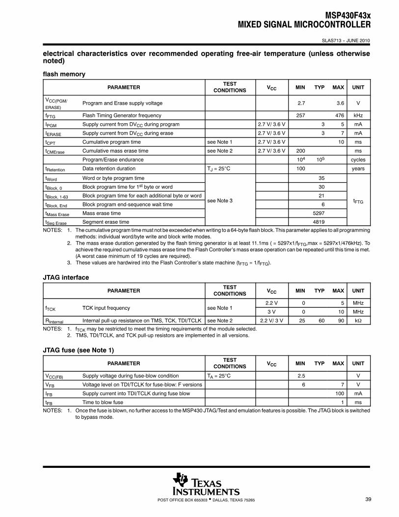
flash memory
PARAMETERTEST
CONDITIONS VCC MIN TYP MAX UNIT
VCC(PGM/ERASE)
Program and Erase supply voltage 2.7 3.6 V
fFTG Flash Timing Generator frequency 257 476 kHz
IPGM Supply current from DVCC during program 2.7 V/ 3.6 V 3 5 mA
IERASE Supply current from DVCC during erase 2.7 V/ 3.6 V 3 7 mA
tCPT Cumulative program time see Note 1 2.7 V/ 3.6 V 10 ms
tCMErase Cumulative mass erase time see Note 2 2.7 V/ 3.6 V 200 ms
Program/Erase endurance 104 105 cycles
tRetention Data retention duration TJ = 25°C 100 years
tWord Word or byte program time 35
tBlock, 0 Block program time for 1st byte or word 30
tBlock, 1-63 Block program time for each additional byte or wordsee Note 3
21t
tBlock, End Block program end-sequence wait timesee Note 3
6tFTG
tMass Erase Mass erase time 5297
tSeg Erase Segment erase time 4819
NOTES: 1. The cumulative program timemust not be exceededwhenwriting to a 64-byte flash block. This parameter applies to all programmingmethods: individual word/byte write and block write modes.
2. The mass erase duration generated by the flash timing generator is at least 11.1ms ( = 5297x1/fFTG,max = 5297x1/476kHz). Toachieve the required cumulativemass erase time the Flash Controller’s mass erase operation can be repeated until this time is met.(A worst case minimum of 19 cycles are required).
3. These values are hardwired into the Flash Controller’s state machine (tFTG = 1/fFTG).
JTAG interface
PARAMETERTEST
CONDITIONS VCC MIN TYP MAX UNIT
f TCK input frequency see Note 12.2 V 0 5 MHz
fTCK TCK input frequency see Note 13 V 0 10 MHz
RInternal Internal pull-up resistance on TMS, TCK, TDI/TCLK see Note 2 2.2 V/ 3 V 25 60 90 kΩ
NOTES: 1. fTCK may be restricted to meet the timing requirements of the module selected.2. TMS, TDI/TCLK, and TCK pull-up resistors are implemented in all versions.
JTAG fuse (see Note 1)
PARAMETERTEST
CONDITIONS VCC MIN TYP MAX UNIT
VCC(FB) Supply voltage during fuse-blow condition TA = 25°C 2.5 V
VFB Voltage level on TDI/TCLK for fuse-blow: F versions 6 7 V
IFB Supply current into TDI/TCLK during fuse blow 100 mA
tFB Time to blow fuse 1 ms
NOTES: 1. Once the fuse is blown, no further access to theMSP430 JTAG/Test and emulation features is possible. The JTAGblock is switchedto bypass mode.
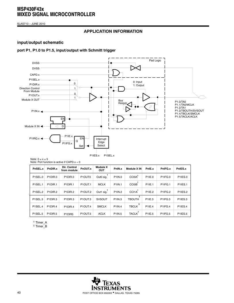
MSP430F43xMIXED SIGNAL MICROCONTROLLER
SLAS713 -- JUNE 2010
40 POST OFFICE BOX 655303 • DALLAS, TEXAS 75265
APPLICATION INFORMATION
input/output schematic
port P1, P1.0 to P1.5, input/output with Schmitt trigger
P1OUT.x
Module X OUT
P1SEL.x
Direction ControlFrom Module
CAPD.x
D
EN
InterruptEdgeSelect
P1IES.x P1SEL.x
P1IE.x
P1IFG.x
P1IRQ.x EN
Set
Q
0
1
1
0
PnSEL.x PnDIR.x Dir. Controlfrom module PnOUT.x Module X
OUT PnIN.x PnIE.x PnIFG.x PnIES.xModule X IN
P1SEL.1 P1DIR.1 P1OUT.1 P1IN.1 P1IE.1 P1IFG.1 P1IES.1
P1SEL.2 P1DIR.2 P1OUT.2 P1IN.2 P1IE.2 P1IFG.2 P1IES.2
P1SEL.0 P1DIR.0 P1OUT0 P1IN.0 P1IE.0 P1IFG.0 P1IES.0Out0 sig. CCI0AP1DIR.0
MCLK
DVSS
Module X IN
P1IN.x
Pad Logic
0: Input1: Output
BusKeeper
Out1 sig. CCI1A
CCI0B
DVSS
†
‡
†
Note: 0 ≤ x ≤ 5Note: Port function is active if CAPD.x = 0
P1DIR.x
P1.0/TA0P1.1/TA0/MCLKP1.2/TA1P1.3/TBOUTH/SVSOUTP1.4/TBCLK/SMCLKP1.5/TACLK/ACLK
P1SEL.4 P1DIR.4 P1OUT.4 P1IN.4 P1IE.4 P1IFG.4 P1IES.4
P1SEL.5 P1DIR.5 P1OUT.5 P1IN.5 P1IE.5 P1IFG.5 P1IES.5
P1SEL.3 P1DIR.3 P1OUT.3 P1IN.3 P1IE.3 P1IFG.3 P1IES.3SVSOUT TBOUTHP1DIR.3
SMCLK
ACLK TACLK
TBCLK
†
†
‡
P1DIR.1
P1DIR.4
P1DIR.2
P1DIR5
†
†
† Timer_A‡ Timer_B
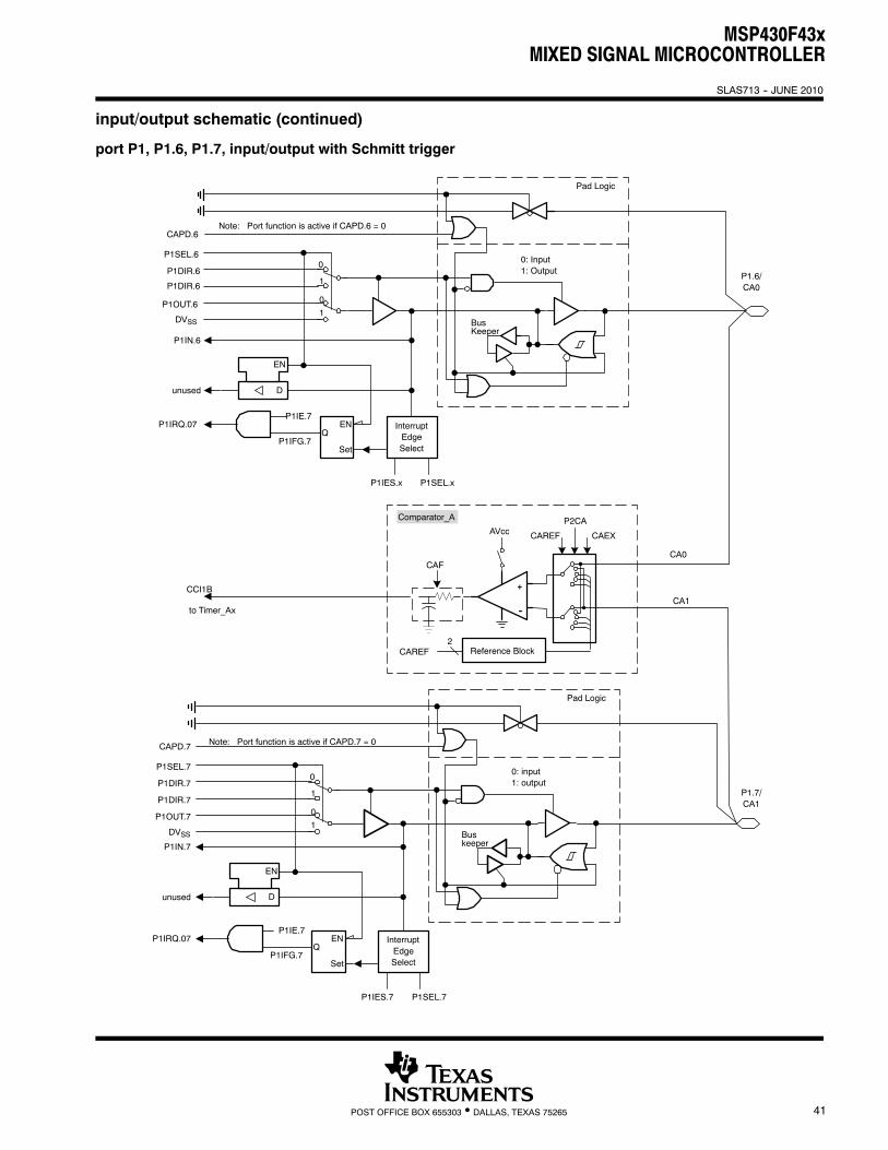
MSP430F43xMIXED SIGNAL MICROCONTROLLER
SLAS713 -- JUNE 2010
41POST OFFICE BOX 655303 • DALLAS, TEXAS 75265
input/output schematic (continued)
port P1, P1.6, P1.7, input/output with Schmitt trigger
P1OUT.7
P1DIR.7
P1SEL.7
D
EN
InterruptEdgeSelect
P1IES.7 P1SEL.7
P1IE.7
P1IFG.7
P1IRQ.07 EN
Set
Q
0
1
1
0
CAPD.7
P1OUT.6
P1DIR.6
P1SEL.6
D
EN
InterruptEdgeSelect
P1IES.x P1SEL.x
P1IE.7
P1IFG.7
P1IRQ.07
P1.6/CA0
EN
Set
Q
0
1
1
0
CAPD.6Note: Port function is active if CAPD.6 = 0
P1IN.6
unused
P1.7/CA1
Comparator_A
Reference Block
CCI1B
CAF
CAREF
P2CA
CAEX
CAREF
to Timer_Ax --
+
2
AVcc
CA0
CA1
Pad Logic
0: Input1: Output
BusKeeper
Pad Logic
0: input1: output
Buskeeper
P1DIR.6
P1DIR.7
P1IN.7
unused
Note: Port function is active if CAPD.7 = 0
DVSS
DVSS
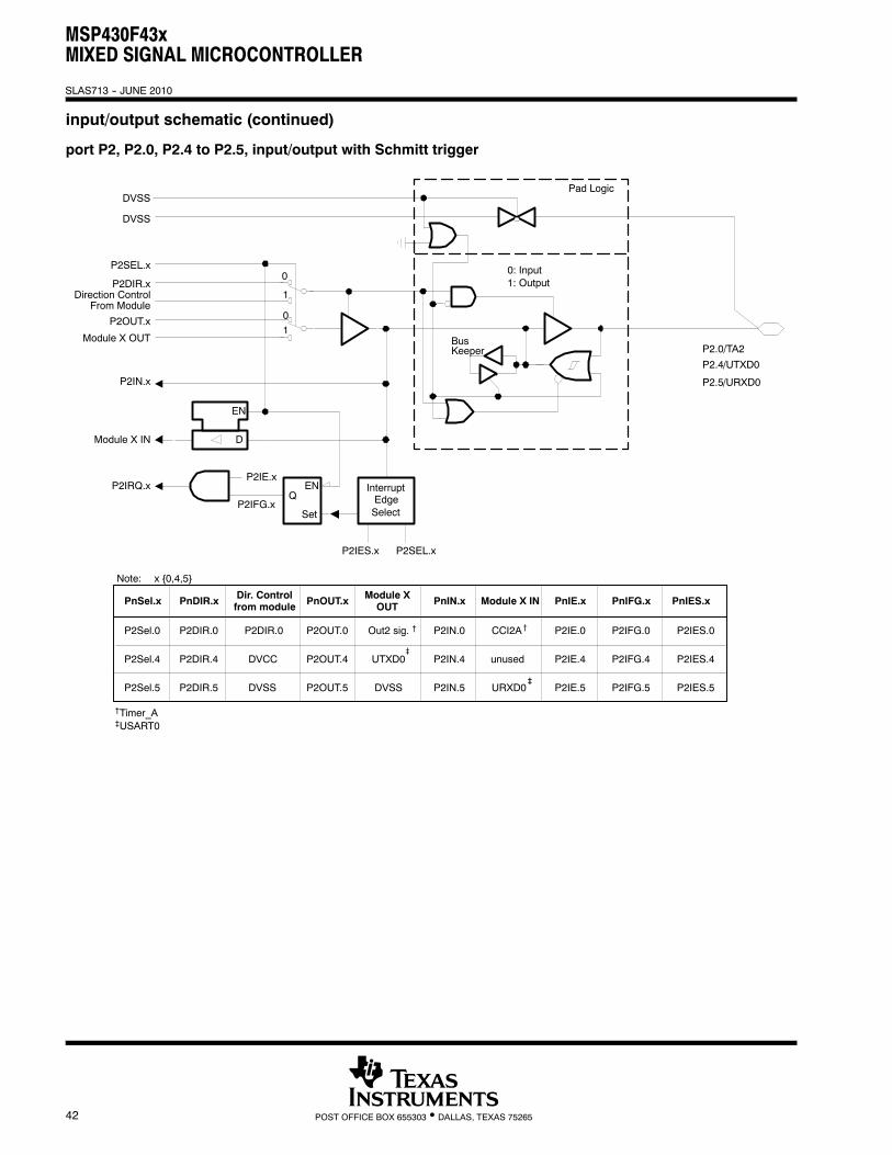
MSP430F43xMIXED SIGNAL MICROCONTROLLER
SLAS713 -- JUNE 2010
42 POST OFFICE BOX 655303 • DALLAS, TEXAS 75265
input/output schematic (continued)
port P2, P2.0, P2.4 to P2.5, input/output with Schmitt trigger
P2OUT.x
Module X OUT
P2DIR.xDirection Control
From Module
P2SEL.x
D
EN
InterruptEdgeSelect
P2IES.x P2SEL.x
P2IE.x
P2IFG.x
P2IRQ.x EN
Set
Q
0
1
1
0
PnSel.x PnDIR.x Dir. Controlfrom module PnOUT.x Module X
OUT PnIN.x PnIE.x PnIFG.x PnIES.xModule X IN
P2Sel.4 P2DIR.4 P2OUT.4 P2IN.4 P2IE.4 P2IFG.4 P2IES.4
P2Sel.5 P2DIR.5 P2OUT.5 P2IN.5 P2IE.5 P2IFG.5 P2IES.5
P2Sel.0 P2DIR.0 P2OUT.0 P2IN.0 P2IE.0 P2IFG.0 P2IES.0Out2 sig. CCI2AP2DIR.0
UTXD0
DVSS
P2.5/URXD0
P2.0/TA2
P2.4/UTXD0
Module X IN
P2IN.x
x 0,4,5Note:
Pad Logic
0: Input1: Output
BusKeeper
DVCC
DVSS DVSS URXD0
unused
DVSS
†Timer_A‡USART0
†
‡
†
‡
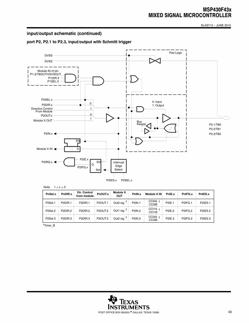
MSP430F43xMIXED SIGNAL MICROCONTROLLER
SLAS713 -- JUNE 2010
43POST OFFICE BOX 655303 • DALLAS, TEXAS 75265
input/output schematic (continued)
port P2, P2.1 to P2.3, input/output with Schmitt trigger
P2OUT.x
Module X OUT
P2DIR.xDirection Control
From Module
P2SEL.x
D
EN
InterruptEdgeSelect
P2IES.x P2SEL.x
P2IE.x
P2IFG.x
P2IRQ.x EN
Set
Q
0
1
1
0
PnSel.x PnDIR.x Dir. Controlfrom module
PnOUT.x Module XOUT
PnIN.x PnIE.x PnIFG.x PnIES.xModule X IN
P2Sel.1 P2DIR.1 P2OUT.1 P2IN.1 P2IE.1 P2IFG.1 P2IES.1
P2Sel.2 P2DIR.2 P2OUT.2 P2IN.2 P2IE.2 P2IFG.2 P2IES.2
P2Sel.3 P2DIR.3 P2OUT.3 P2IN.3 P2IE.3 P2IFG.3 P2IES.3
P2DIR.1
P2DIR.2
P2.1/TB0
P2.2/TB1
P2.3/TB2
Out0 sig.
Module X IN
P2IN.x
1 < x < 3Note:
Pad Logic
0: Input1: Output
BusKeeper
P2DIR.3 Out2 sig.
Out1 sig.
CCI0ACCI0B
CCI1ACCI1B
CCI2ACCI2B
DVSS
DVSS
Module IN of pinP1.3/TBOUTH/SVSOUT
P1SEL.3P1DIR.3
†Timer_B
†
†
†
†
†
†
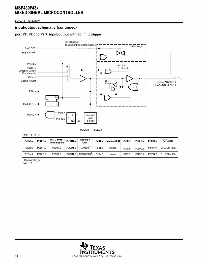
MSP430F43xMIXED SIGNAL MICROCONTROLLER
SLAS713 -- JUNE 2010
44 POST OFFICE BOX 655303 • DALLAS, TEXAS 75265
input/output schematic (continued)
port P2, P2.6 to P2.7, input/output with Schmitt trigger
P2OUT.x
Module X OUT
P2DIR.xDirection Control
From Module
P2SEL.x
D
EN
InterruptEdgeSelect
P2IES.x P2SEL.x
P2IE.x
P2IFG.x
P2IRQ.x EN
Set
Q
0
1
1
0
PnSel.x PnDIR.x Dir. Controlfrom module
PnOUT.x Module XOUT
PnIN.x PnIE.x PnIFG.x PnIES.xModule X IN
0: Port active1: Segment xx function active
P2Sel.6 P2DIR.6
P2Sel.7 P2DIR.7
P2DIR.6
P2DIR.7
P2OUT.6
P2OUT.7
P2IN.6
P2IN.7 unused
CAOUT
ADC12CLK
P2IE.6
P2IE.7
P2IFG.6
P2IFG.7
P2IES.6
P2IES.7
Module X IN
P2IN.x
6 < x < 7Note:
Pad Logic
0: Input1: Output
BusKeeper
unused
Port/LCD
0: LCDM<40h
0: LCDM<40h
Port/LCD‡
Segment xx‡
P2.6/CAOUT/S19P2.7/ADC12CLK/S18
†
§
† Comparator_A§ ADC12
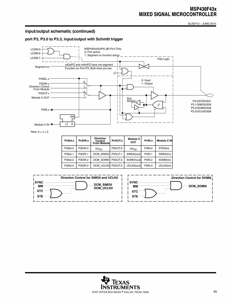
MSP430F43xMIXED SIGNAL MICROCONTROLLER
SLAS713 -- JUNE 2010
45POST OFFICE BOX 655303 • DALLAS, TEXAS 75265
input/output schematic (continued)
port P3, P3.0 to P3.3, input/output with Schmitt trigger
P3OUT.x
Module X OUT
P3DIR.xDirection Control
From Module
P3SEL.x
D
EN
0
1
1
0
PnSel.x PnDIR.x PnOUT.xModule XOUT
PnIN.x Module X IN
P3Sel.1 P3DIR.1 P3OUT.1 P3IN.1
P3Sel.2 P3DIR.2 P3OUT.2 P3IN.2
P3Sel.3 P3DIR.3 P3OUT.3 P3IN.3
P3Sel.0 P3DIR.0 P3OUT.0 P3IN.0
UCLK0(out)
SOMIO(out)
DCM_SIMO0
DCM_SOMI0
DCM_UCLK0
Segment xx
0: Port active1: Segment xx function active
SIMO0(out)
UCLK0(in)
SOMI0(in)
SIMO0(in)
STE0(in)
Module X IN
P3IN.x
Pad Logic
0: Input1: Output
BusKeeper
LCDM.5LCDM.6
LCDM.7
Direction
From ModuleControl
DVSSDVSS
MSP430x43xIPN (80-Pin) Only
x43xIPZ and x44xIPZ have not segmentFunction on Port P3: Both lines are low.
P3.0/STE0/S31P3.1/SIMO0/S30P3.2/SOMI0/S29P3.3/UCLK0/S28
Note: 0 ≤ x ≤ 3
SYNCMM
STC
STE
SYNCMM
STC
STE
DCM_SOMI0DCM_SIMO0DCM_UCLK0
Direction Control for SOMI0Direction Control for SIMO0 and UCLK0
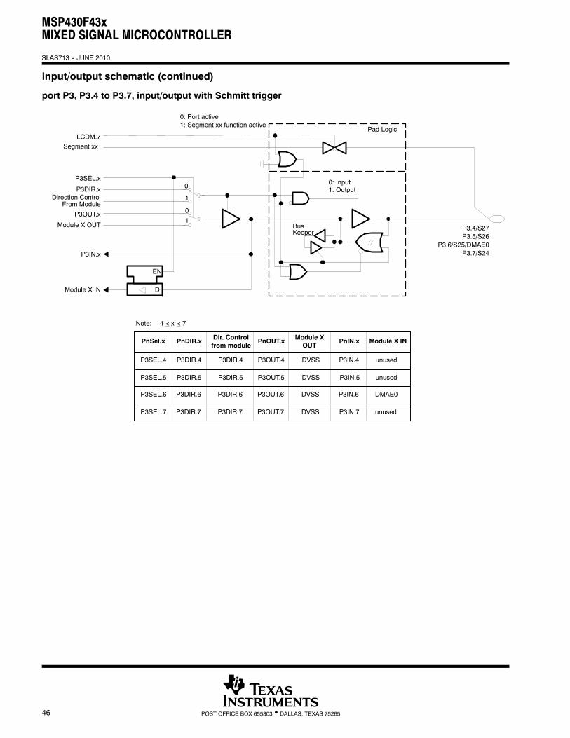
MSP430F43xMIXED SIGNAL MICROCONTROLLER
SLAS713 -- JUNE 2010
46 POST OFFICE BOX 655303 • DALLAS, TEXAS 75265
input/output schematic (continued)
port P3, P3.4 to P3.7, input/output with Schmitt trigger
P3OUT.x
Module X OUT
P3DIR.xDirection Control
From Module
P3SEL.x
D
EN
0
1
1
0
PnSel.x PnDIR.x Dir. Controlfrom module
PnOUT.x Module XOUT
PnIN.x Module X IN
0: Port active1: Segment xx function active
P3SEL.4 P3DIR.4
P3SEL.5 P3DIR.5
P3DIR.4
P3DIR.5
P3OUT.4
P3OUT.5
P3IN.4
P3IN.5 unused
DVSS
DVSS
Module X IN
P3IN.x
4 < x < 7Note:
Pad Logic
0: Input1: Output
BusKeeper
unused
Segment xx
P3.4/S27P3.5/S26
P3.6/S25/DMAE0P3.7/S24
LCDM.7
P3SEL.6 P3DIR.6
P3SEL.7 P3DIR.7
P3DIR.6
P3DIR.7
P3OUT.6
P3OUT.7
P3IN.6
P3IN.7 unused
DVSS
DVSS
DMAE0
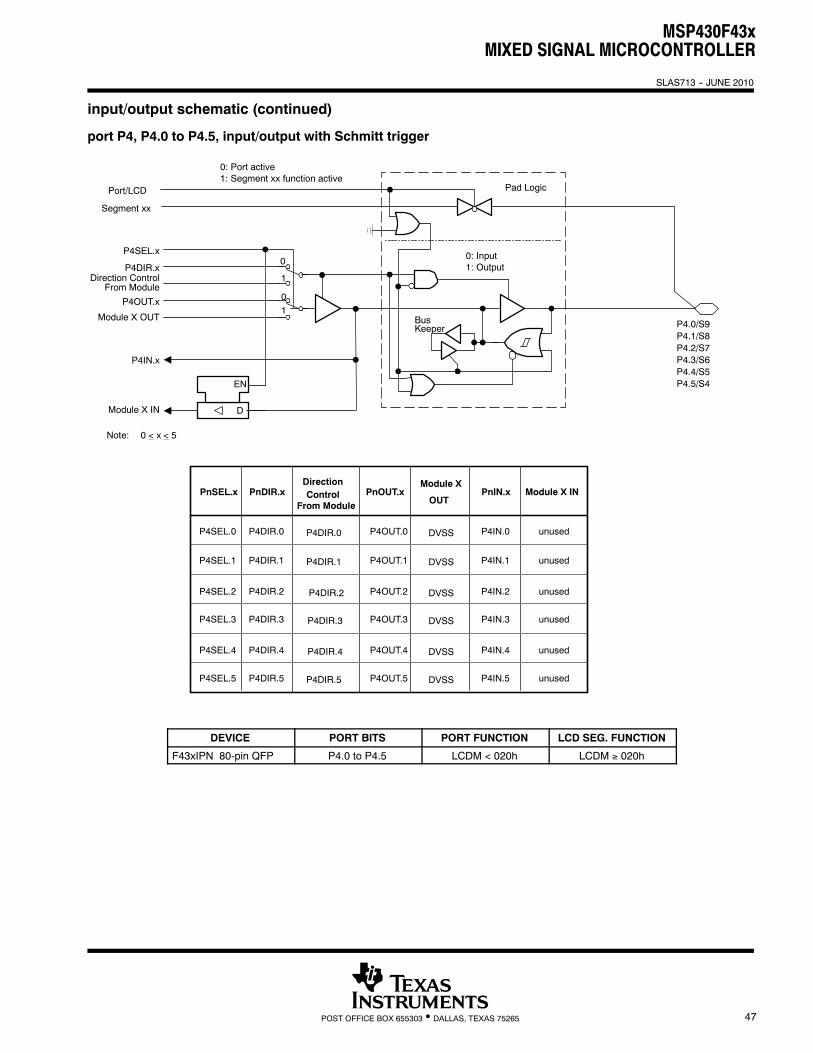
MSP430F43xMIXED SIGNAL MICROCONTROLLER
SLAS713 -- JUNE 2010
47POST OFFICE BOX 655303 • DALLAS, TEXAS 75265
input/output schematic (continued)
port P4, P4.0 to P4.5, input/output with Schmitt trigger
P4OUT.x
Module X OUT
P4DIR.xDirection Control
From Module
P4SEL.x
D
EN
0
1
1
0
PnSEL.x PnDIR.x PnOUT.xModule X
OUTPnIN.x Module X IN
P4SEL.1 P4DIR.1 P4OUT.1 P4IN.1
P4SEL.2 P4DIR.2 P4OUT.2 P4IN.2
P4SEL.3 P4DIR.3 P4OUT.3 P4IN.3
P4SEL.4 P4DIR.4 P4OUT.4 P4IN.4
P4SEL.5 P4DIR.5 P4OUT.5 P4IN.5
P4SEL.0 P4DIR.0 P4OUT.0 P4IN.0
Segment xx
0: Port active1: Segment xx function active
Module X IN
P4IN.x
0 < x < 5Note:
Pad Logic
0: Input1: Output
BusKeeper
Direction
From ModuleControl
DVSS
DVSS
DVSS
Port/LCD
P4.0/S9P4.1/S8P4.2/S7P4.3/S6P4.4/S5P4.5/S4
P4DIR.0
P4DIR.1
P4DIR.2
P4DIR.3
P4DIR.4
P4DIR.5
DVSS
DVSS
DVSS
unused
unused
unused
unused
unused
unused
DEVICE PORT BITS PORT FUNCTION LCD SEG. FUNCTION
F43xIPN 80-pin QFP P4.0 to P4.5 LCDM < 020h LCDM ≥ 020h
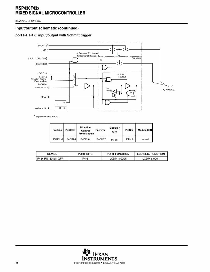
MSP430F43xMIXED SIGNAL MICROCONTROLLER
SLAS713 -- JUNE 2010
48 POST OFFICE BOX 655303 • DALLAS, TEXAS 75265
input/output schematic (continued)
port P4, P4.6, input/output with Schmitt trigger
PnSEL.x PnDIR.x PnOUT.xModule X
OUTPnIN.x Module X IN
P4SEL.6 P4DIR.6 P4DIR.6 P4OUT.6 P4IN.6 unused
Direction
From ModuleControl
DVSS
P4OUT.6
Module XOUT
P4DIR.6Direction Control
From Module
P4SEL.6
D
EN
0
1
1
0
Segment S3
1, if LCDM > 020h
0: Segment S3 disabled1: Segment S3 enabled
Module X IN
P4IN.6
Pad Logic
0: input1: output
Buskeeper P4.6/S3/A15
INCH=15#
a15 #
# Signal from or to ADC12
DEVICE PORT BITS PORT FUNCTION LCD SEG. FUNCTION
F43xIPN 80-pin QFP P4.6 LCDM < 020h LCDM ≥ 020h
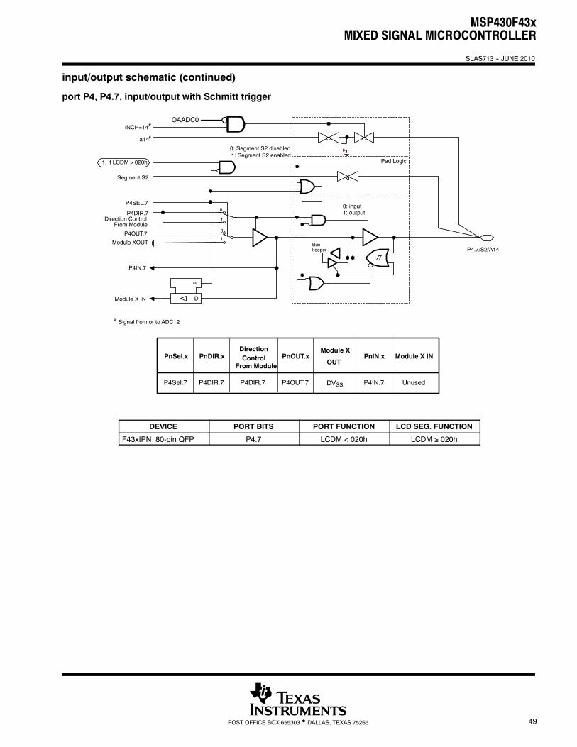
MSP430F43xMIXED SIGNAL MICROCONTROLLER
SLAS713 -- JUNE 2010
49POST OFFICE BOX 655303 • DALLAS, TEXAS 75265
input/output schematic (continued)
port P4, P4.7, input/output with Schmitt trigger
PnSel.x PnDIR.x PnOUT.xModule X
OUTPnIN.x Module X IN
P4Sel.7 P4DIR.7 P4DIR.7 P4OUT.7 P4IN.7 Unused
Direction
From ModuleControl
DVSS
P4OUT.7
Module XOUT
P4DIR.7Direction Control
From Module
P4SEL.7
D
EN
0
1
1
0
Segment S2
1, if LCDM > 020h
0: Segment S2 disabled1: Segment S2 enabled
Module X IN
P4IN.7
Pad Logic
0: input1: output
Buskeeper P4.7/S2/A14
INCH=14#
a14#
# Signal from or to ADC12
OAADC0
DEVICE PORT BITS PORT FUNCTION LCD SEG. FUNCTION
F43xIPN 80-pin QFP P4.7 LCDM < 020h LCDM ≥ 020h
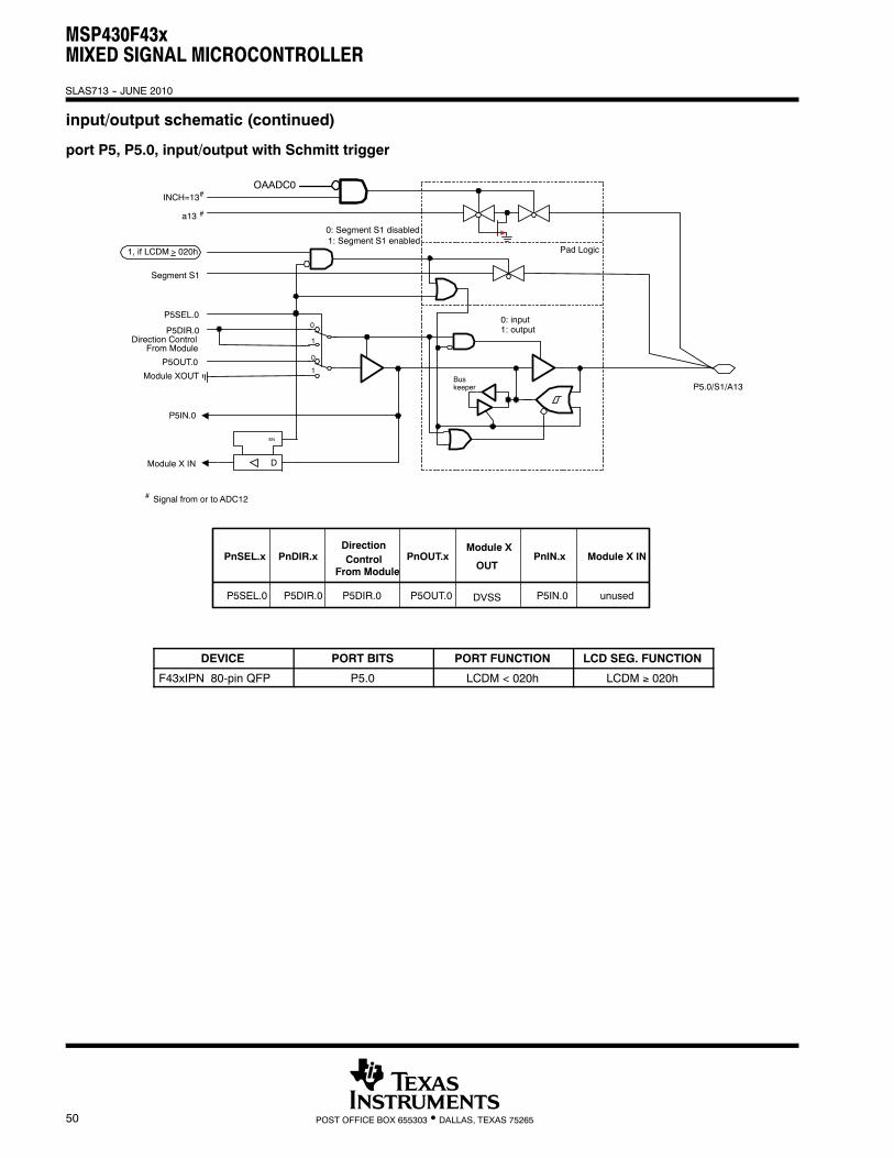
MSP430F43xMIXED SIGNAL MICROCONTROLLER
SLAS713 -- JUNE 2010
50 POST OFFICE BOX 655303 • DALLAS, TEXAS 75265
input/output schematic (continued)
port P5, P5.0, input/output with Schmitt trigger
PnSEL.x PnDIR.x PnOUT.xModule X
OUTPnIN.x Module X IN
P5SEL.0 P5DIR.0 P5DIR.0 P5OUT.0 P5IN.0 unused
Direction
From ModuleControl
DVSS
P5OUT.0
Module XOUT
P5DIR.0Direction Control
From Module
P5SEL.0
D
EN
0
1
1
0
Segment S1
1, if LCDM > 020h
0: Segment S1 disabled1: Segment S1 enabled
Module X IN
P5IN.0
Pad Logic
0: input1: output
Buskeeper P5.0/S1/A13
INCH=13#
a13 #
# Signal from or to ADC12
OAADC0
DEVICE PORT BITS PORT FUNCTION LCD SEG. FUNCTION
F43xIPN 80-pin QFP P5.0 LCDM < 020h LCDM ≥ 020h
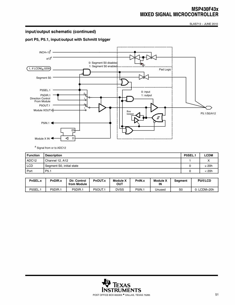
MSP430F43xMIXED SIGNAL MICROCONTROLLER
SLAS713 -- JUNE 2010
51POST OFFICE BOX 655303 • DALLAS, TEXAS 75265
input/output schematic (continued)
port P5, P5.1, input/output with Schmitt trigger
P5OUT.1
Module XOUT
P5DIR.1Direction Control
From Module
P5SEL.1
D
EN
0
1
1
0
Segment S0
1, if LCDM> 020h
0: Segment S0 disabled1: Segment S0 enabled
Module X IN
P5IN.1
Pad Logic
0: input1: output
Buskeeper P5.1/S0/A12
INCH=12#
a12#
# Signal from or to ADC12
Function Description P5SEL.1 LCDM
ADC12 Channel 12, A12 1 X
LCD Segment S0, initial state 0 ≥ 20h
Port P5.1 0 < 20h
PnSEL.x PnDIR.x Dir. Controlfrom Module
PnOUT.x Module XOUT
PnIN.x Module XIN
Segment Port/LCD
P5SEL.1 P5DIR.1 P5DIR.1 P5OUT.1 DVSS P5IN.1 Unused S0 0: LCDM<20h
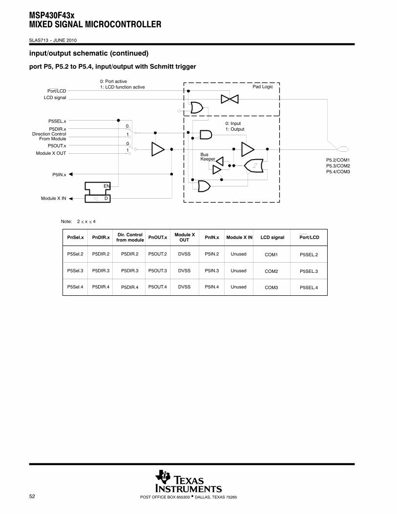
MSP430F43xMIXED SIGNAL MICROCONTROLLER
SLAS713 -- JUNE 2010
52 POST OFFICE BOX 655303 • DALLAS, TEXAS 75265
input/output schematic (continued)
port P5, P5.2 to P5.4, input/output with Schmitt trigger
P5OUT.x
Module X OUT
P5DIR.xDirection Control
From Module
P5SEL.x
D
EN
0
1
1
0
PnSel.x PnDIR.x Dir. Controlfrom module PnOUT.x Module X
OUT PnIN.x Module X IN
P5Sel.2 P5DIR.2 P5OUT.2 P5IN.2
P5Sel.3 P5DIR.3 P5OUT.3 P5IN.3
P5Sel.4 P5DIR.4 P5OUT.4 P5IN.4
DVSS
DVSS
DVSS
LCD signal
0: Port active1: LCD function active
LCD signal
Unused
Unused
Unused
Module X IN
P5IN.x
2 < x < 4Note:
Pad Logic
0: Input1: Output
BusKeeper
P5DIR.3
P5DIR.2
P5DIR.4
Port/LCD
Port/LCD
P5.2/COM1P5.3/COM2P5.4/COM3
COM1
COM2
COM3
P5SEL.2
P5SEL.3
P5SEL.4
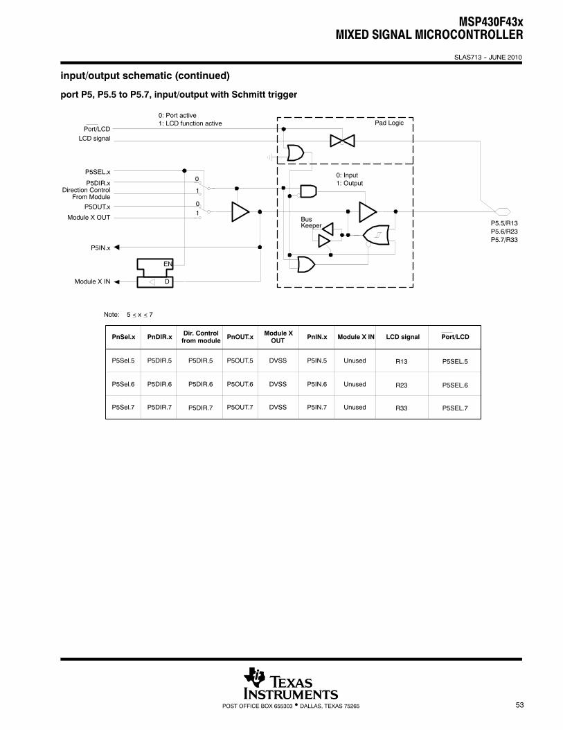
MSP430F43xMIXED SIGNAL MICROCONTROLLER
SLAS713 -- JUNE 2010
53POST OFFICE BOX 655303 • DALLAS, TEXAS 75265
input/output schematic (continued)
port P5, P5.5 to P5.7, input/output with Schmitt trigger
P5OUT.x
Module X OUT
P5DIR.xDirection Control
From Module
P5SEL.x
D
EN
0
1
1
0
PnSel.x PnDIR.x Dir. Controlfrom module PnOUT.x Module X
OUT PnIN.x Module X IN
P5Sel.5 P5DIR.5 P5OUT.5 P5IN.5
P5Sel.6 P5DIR.6 P5OUT.6 P5IN.6
P5Sel.7 P5DIR.7 P5OUT.7 P5IN.7
DVSS
DVSS
DVSS
LCD signal
0: Port active1: LCD function active
LCD signal
Unused
Unused
Unused
Module X IN
P5IN.x
5 < x < 7Note:
Pad Logic
0: Input1: Output
BusKeeper
P5DIR.6
P5DIR.5
P5DIR.7
Port/LCD
Port/LCD
R13 P5SEL.5
P5.5/R13P5.6/R23P5.7/R33
R23
R33
P5SEL.6
P5SEL.7
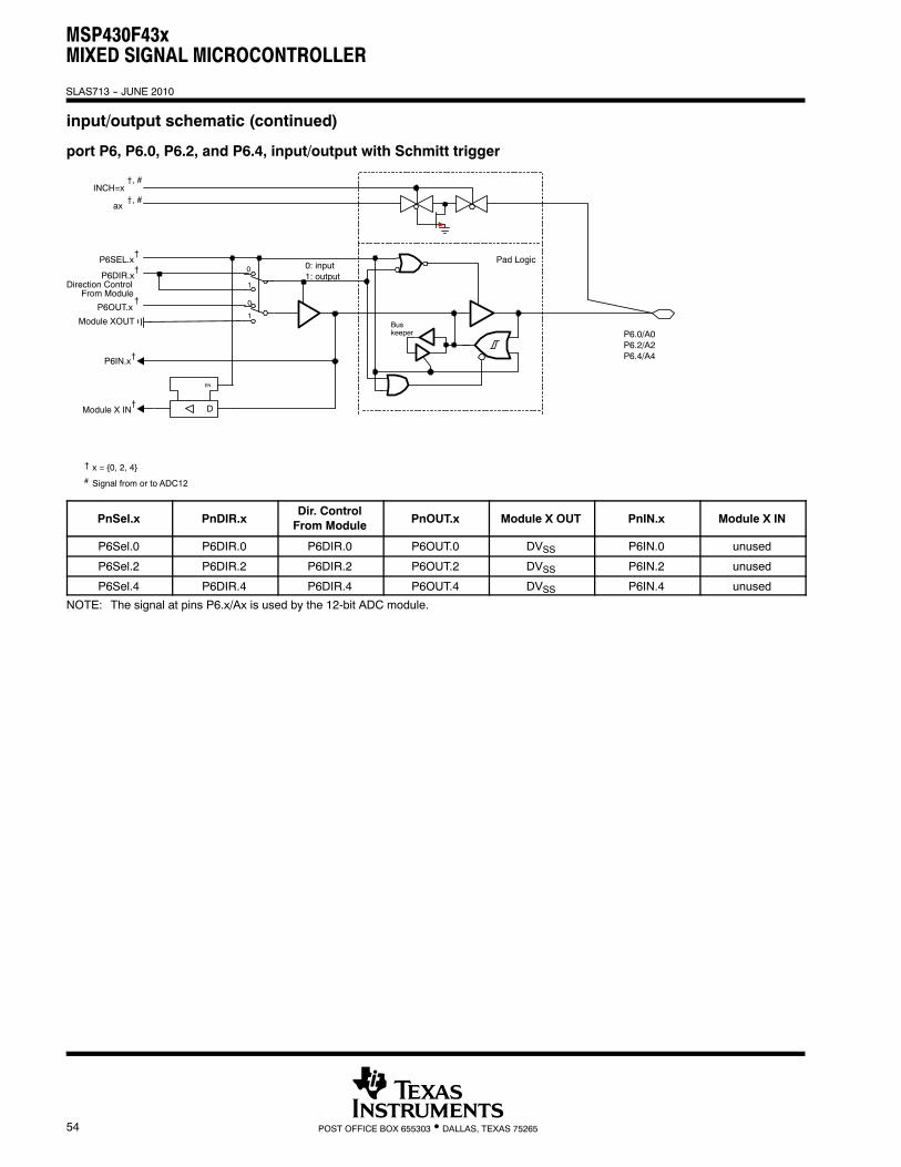
MSP430F43xMIXED SIGNAL MICROCONTROLLER
SLAS713 -- JUNE 2010
54 POST OFFICE BOX 655303 • DALLAS, TEXAS 75265
input/output schematic (continued)
port P6, P6.0, P6.2, and P6.4, input/output with Schmitt trigger
P6OUT.x
Module XOUT
P6DIR.xDirection Control
From Module
P6SEL.x
D
EN
0
1
1
0
Module X IN
P6IN.x
Pad Logic0: input1: output
Buskeeper P6.0/A0
P6.2/A2P6.4/A4
INCH=x
ax
# Signal from or to ADC12
† x = 0, 2, 4
†
†, #
†
†
†, #
†
†
PnSel.x PnDIR.xDir. ControlFrom Module PnOUT.x Module X OUT PnIN.x Module X IN
P6Sel.0 P6DIR.0 P6DIR.0 P6OUT.0 DVSS P6IN.0 unused
P6Sel.2 P6DIR.2 P6DIR.2 P6OUT.2 DVSS P6IN.2 unused
P6Sel.4 P6DIR.4 P6DIR.4 P6OUT.4 DVSS P6IN.4 unused
NOTE: The signal at pins P6.x/Ax is used by the 12-bit ADC module.
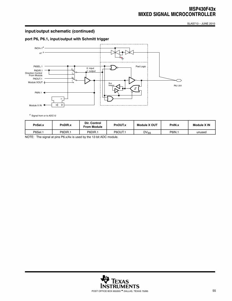
MSP430F43xMIXED SIGNAL MICROCONTROLLER
SLAS713 -- JUNE 2010
55POST OFFICE BOX 655303 • DALLAS, TEXAS 75265
input/output schematic (continued)
port P6, P6.1, input/output with Schmitt trigger
P6OUT.1
Module XOUT
P6DIR.1Direction Control
From Module
P6SEL.1
D
EN
0
1
1
0
Module X IN
P6IN.1
Pad Logic0: input1: output
Buskeeper P6.1/A1
INCH=1#
a1 #
# Signal from or to ADC12
PnSel.x PnDIR.xDir. ControlFrom Module PnOUT.x Module X OUT PnIN.x Module X IN
P6Sel.1 P6DIR.1 P6DIR.1 P6OUT.1 DVSS P6IN.1 unused
NOTE: The signal at pins P6.x/Ax is used by the 12-bit ADC module.
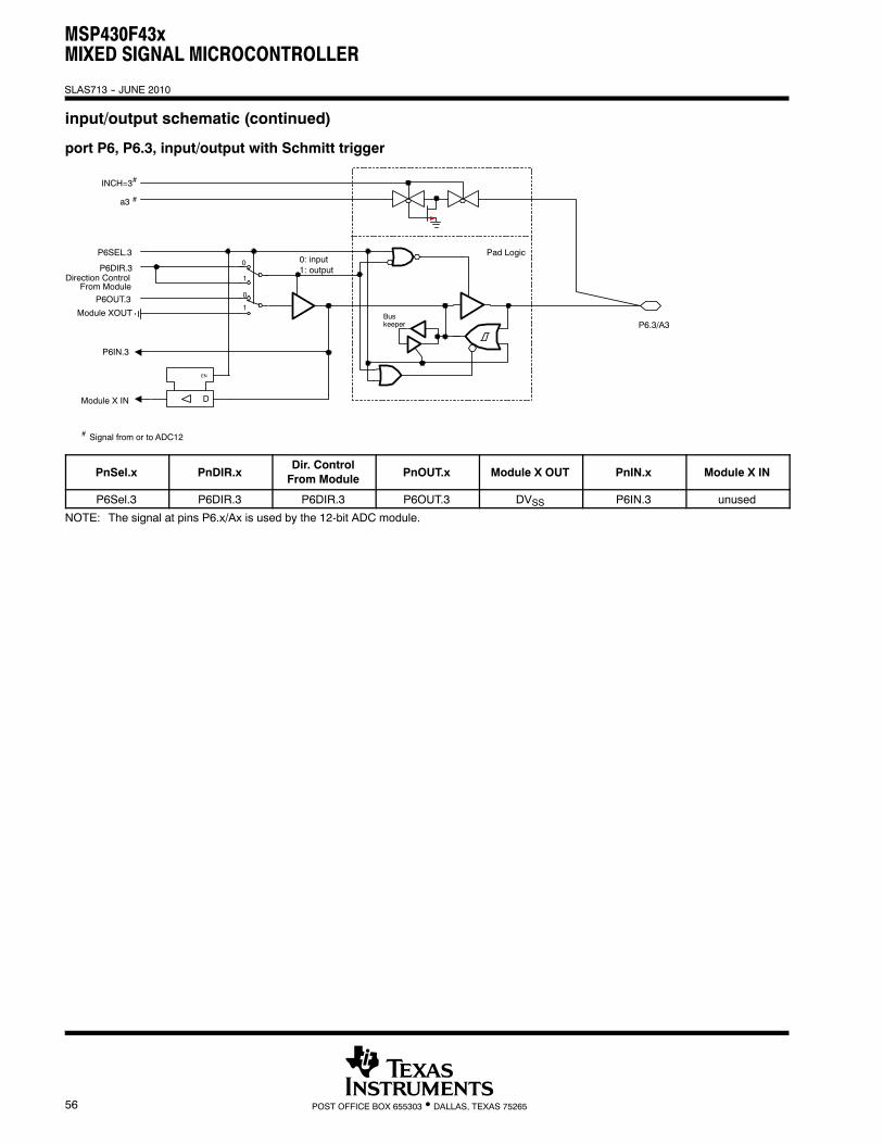
MSP430F43xMIXED SIGNAL MICROCONTROLLER
SLAS713 -- JUNE 2010
56 POST OFFICE BOX 655303 • DALLAS, TEXAS 75265
input/output schematic (continued)
port P6, P6.3, input/output with Schmitt trigger
P6OUT.3
Module XOUT
P6DIR.3Direction Control
From Module
P6SEL.3
D
EN
0
1
1
0
Module X IN
P6IN.3
Pad Logic0: input1: output
Buskeeper P6.3/A3
INCH=3#
a3 #
# Signal from or to ADC12
PnSel.x PnDIR.xDir. ControlFrom Module PnOUT.x Module X OUT PnIN.x Module X IN
P6Sel.3 P6DIR.3 P6DIR.3 P6OUT.3 DVSS P6IN.3 unused
NOTE: The signal at pins P6.x/Ax is used by the 12-bit ADC module.
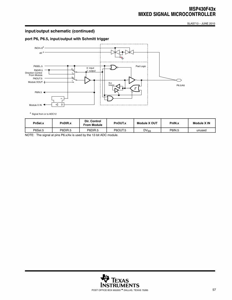
MSP430F43xMIXED SIGNAL MICROCONTROLLER
SLAS713 -- JUNE 2010
57POST OFFICE BOX 655303 • DALLAS, TEXAS 75265
input/output schematic (continued)
port P6, P6.5, input/output with Schmitt trigger
P6OUT.5
Module XOUT
P6DIR.5Direction Control
From Module
P6SEL.5
D
EN
0
1
1
0
Module X IN
P6IN.5
Pad Logic0: input1: output
Buskeeper P6.5/A5
INCH=5#
a5 #
# Signal from or to ADC12
PnSel.x PnDIR.xDir. ControlFrom Module PnOUT.x Module X OUT PnIN.x Module X IN
P6Sel.5 P6DIR.5 P6DIR.5 P6OUT.5 DVSS P6IN.5 unused
NOTE: The signal at pins P6.x/Ax is used by the 12-bit ADC module.
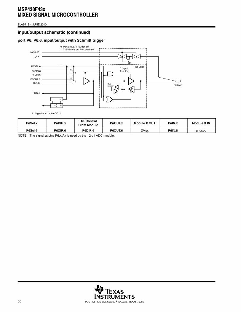
MSP430F43xMIXED SIGNAL MICROCONTROLLER
SLAS713 -- JUNE 2010
58 POST OFFICE BOX 655303 • DALLAS, TEXAS 75265
input/output schematic (continued)
port P6, P6.6, input/output with Schmitt trigger
P6OUT.6
DVSS
P6DIR.6
P6DIR.6
P6SEL.6
D
EN
0
1
1
0
INCH=6#
0: Port active, T--Switch off1: T--Switch is on, Port disabled
P6IN.6
a6 #
Pad Logic0: input1: output
Buskeeper
# Signal from or to ADC12
P6.6/A6
PnSel.x PnDIR.xDir. ControlFrom Module PnOUT.x Module X OUT PnIN.x Module X IN
P6Sel.6 P6DIR.6 P6DIR.6 P6OUT.6 DVSS P6IN.6 unused
NOTE: The signal at pins P6.x/Ax is used by the 12-bit ADC module.
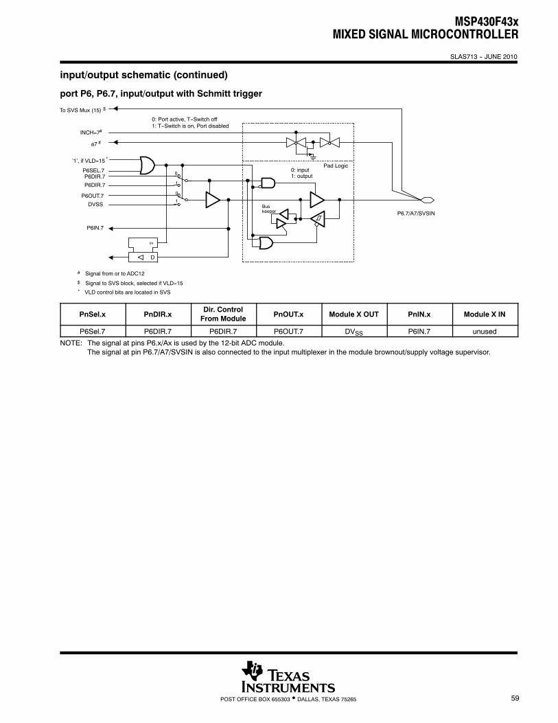
MSP430F43xMIXED SIGNAL MICROCONTROLLER
SLAS713 -- JUNE 2010
59POST OFFICE BOX 655303 • DALLAS, TEXAS 75265
input/output schematic (continued)
port P6, P6.7, input/output with Schmitt trigger
P6OUT.7
DVSS
P6DIR.7
P6DIR.7
P6SEL.7
D
EN
0
1
1
0
INCH=7#
0: Port active, T--Switch off1: T--Switch is on, Port disabled
P6.7/A7/SVSIN
P6IN.7
a7 #
Pad Logic0: input1: output
Buskeeper
# Signal from or to ADC12
To SVS Mux (15) $
$ Signal to SVS block, selected if VLD=15
’1’, if VLD=15 *
* VLD control bits are located in SVS
PnSel.x PnDIR.xDir. ControlFrom Module PnOUT.x Module X OUT PnIN.x Module X IN
P6Sel.7 P6DIR.7 P6DIR.7 P6OUT.7 DVSS P6IN.7 unused
NOTE: The signal at pins P6.x/Ax is used by the 12-bit ADC module.The signal at pin P6.7/A7/SVSIN is also connected to the input multiplexer in the module brownout/supply voltage supervisor.
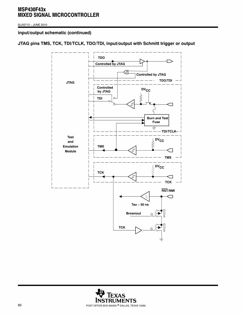
MSP430F43xMIXED SIGNAL MICROCONTROLLER
SLAS713 -- JUNE 2010
60 POST OFFICE BOX 655303 • DALLAS, TEXAS 75265
input/output schematic (continued)
JTAG pins TMS, TCK, TDI/TCLK, TDO/TDI, input/output with Schmitt trigger or output
TDI
TDO
TMS
TDI/TCLK
TDO/TDI
Controlledby JTAG
TCK
TMS
TCK
DVCC
Controlled by JTAG
Test
JTAG
andEmulationModule
DVCC
DVCC
Burn and TestFuse
RST/NMI
GD
SU
GD
SUTCK
Tau ~ 50 ns
Brownout
Controlled by JTAG
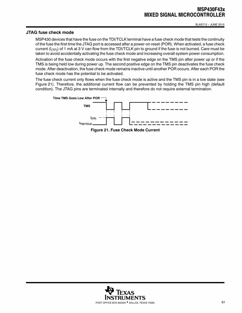
MSP430F43xMIXED SIGNAL MICROCONTROLLER
SLAS713 -- JUNE 2010
61POST OFFICE BOX 655303 • DALLAS, TEXAS 75265
JTAG fuse check mode
MSP430 devices that have the fuse on the TDI/TCLK terminal have a fuse checkmode that tests the continuityof the fuse the first time the JTAG port is accessed after a power-on reset (POR).When activated, a fuse checkcurrent (I(TF)) of 1 mA at 3 V can flow from the TDI/TCLK pin to ground if the fuse is not burned. Care must betaken to avoid accidentally activating the fuse check mode and increasing overall system power consumption.Activation of the fuse check mode occurs with the first negative edge on the TMS pin after power up or if theTMS is being held low during power up. The second positive edge on the TMS pin deactivates the fuse checkmode. After deactivation, the fuse check mode remains inactive until another POR occurs. After each POR thefuse check mode has the potential to be activated.The fuse check current only flows when the fuse check mode is active and the TMS pin is in a low state (seeFigure 21). Therefore, the additional current flow can be prevented by holding the TMS pin high (defaultcondition). The JTAG pins are terminated internally and therefore do not require external termination.
Time TMS Goes Low After POR
TMS
I(TF)ITDI/TCLK
Figure 21. Fuse Check Mode Current
MSP430F43xMIXED SIGNAL MICROCONTROLLER
SLAS713 -- JUNE 2010
62 POST OFFICE BOX 655303 • DALLAS, TEXAS 75265
Revision History
LiteratureNumber Summary
SLAS713 Production Data release
NOTE: Page and figure numbers refer to the respective document revision.
Manual Update SheetSLAZ560–December 2013
Corrections to MSP430F438, MSP430F439 Data Sheet(SLAS713)
Document Being Updated: MSP430F438, MSP430F439 Mixed Signal Microcontroller
Literature Number Being Updated: SLAS713
Page Change or Add44 In both entries in the "Port/LCD" column of the table:
0: LCDM < 40h should be changed to 0: LCDPx < 02h.45 In the top left of the figure:
LCDM.5 should be changed to bit 0 of LCDPx, which is bit 5 of the LCDCTL register.LCDM.6 should be changed to bit 1 of LCDPx, which is bit 6 of the LCDCTL register.LCDM.7 should be changed to bit 2 of LCDPx, which is bit 7 of the LCDCTL register.
46 In the top left of the figure:LCDM.7 should be changed to bit 2 of LCDPx, which is bit 7 of the LCDCTL register.
47 In the table at the bottom of the page:LCDM < 020h should be changed to LCDPx < 01h.LCDM ≥ 020h should be changed to LCDPx ≥ 01h.
48 In the top left of the figure:LCDM ≥ 020h should be changed to LCDPx ≥ 01h.In the table at the bottom of the page:LCDM < 020h should be changed to LCDPx < 01h.LCDM ≥ 020h should be changed to LCDPx ≥ 01h.
49 In the top left of the figure:LCDM ≥ 020h should be changed to LCDPx ≥ 01h.In the table at the bottom of the page:LCDM < 020h should be changed to LCDPx < 01h.LCDM ≥ 020h should be changed to LCDPx ≥ 01h.
50 In the top left of the figure:LCDM ≥ 020h should be changed to LCDPx ≥ 01hIn the table at the bottom of the page:LCDM < 020h should be changed to LCDPx < 01h.LCDM ≥ 020h should be changed to LCDPx ≥ 01h.
51 In the top left of the figure:LCDM ≥ 020h should be changed to LCDPx ≥ 01h.In the first table on the page:The LCDM column heading should be changed to LCDPx.≥ 20h should be changed to ≥ 01h.< 20h should be changed to < 01h.In the "Port/LCD" column of the table on the bottom of the page:0: LCDM < 20h should be changed to 0: LCDPx < 01h.
1SLAZ560–December 2013 Corrections to MSP430F438, MSP430F439 Data Sheet (SLAS713)Submit Documentation Feedback
Copyright © 2013, Texas Instruments Incorporated
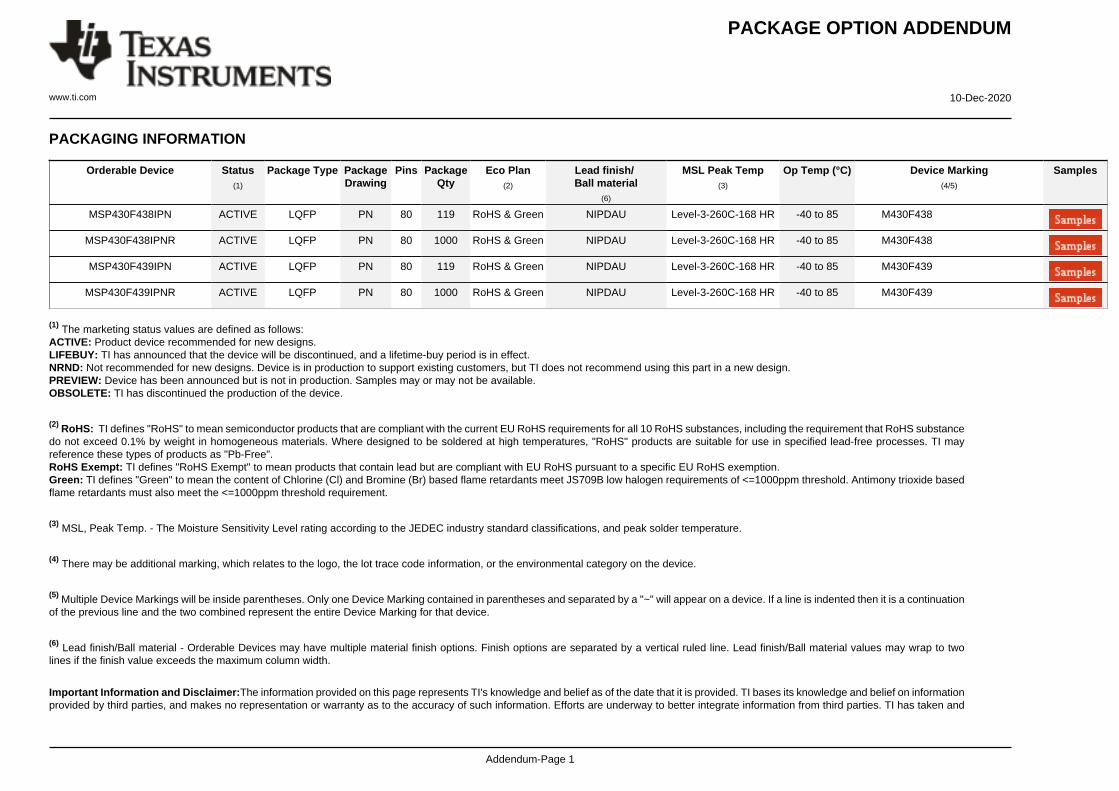
PACKAGE OPTION ADDENDUM
www.ti.com 10-Dec-2020
Addendum-Page 1
PACKAGING INFORMATION
Orderable Device Status(1)
Package Type PackageDrawing
Pins PackageQty
Eco Plan(2)
Lead finish/Ball material
(6)
MSL Peak Temp(3)
Op Temp (°C) Device Marking(4/5)
Samples
MSP430F438IPN ACTIVE LQFP PN 80 119 RoHS & Green NIPDAU Level-3-260C-168 HR -40 to 85 M430F438
MSP430F438IPNR ACTIVE LQFP PN 80 1000 RoHS & Green NIPDAU Level-3-260C-168 HR -40 to 85 M430F438
MSP430F439IPN ACTIVE LQFP PN 80 119 RoHS & Green NIPDAU Level-3-260C-168 HR -40 to 85 M430F439
MSP430F439IPNR ACTIVE LQFP PN 80 1000 RoHS & Green NIPDAU Level-3-260C-168 HR -40 to 85 M430F439
(1) The marketing status values are defined as follows:ACTIVE: Product device recommended for new designs.LIFEBUY: TI has announced that the device will be discontinued, and a lifetime-buy period is in effect.NRND: Not recommended for new designs. Device is in production to support existing customers, but TI does not recommend using this part in a new design.PREVIEW: Device has been announced but is not in production. Samples may or may not be available.OBSOLETE: TI has discontinued the production of the device.
(2) RoHS: TI defines "RoHS" to mean semiconductor products that are compliant with the current EU RoHS requirements for all 10 RoHS substances, including the requirement that RoHS substancedo not exceed 0.1% by weight in homogeneous materials. Where designed to be soldered at high temperatures, "RoHS" products are suitable for use in specified lead-free processes. TI mayreference these types of products as "Pb-Free".RoHS Exempt: TI defines "RoHS Exempt" to mean products that contain lead but are compliant with EU RoHS pursuant to a specific EU RoHS exemption.Green: TI defines "Green" to mean the content of Chlorine (Cl) and Bromine (Br) based flame retardants meet JS709B low halogen requirements of <=1000ppm threshold. Antimony trioxide basedflame retardants must also meet the <=1000ppm threshold requirement.
(3) MSL, Peak Temp. - The Moisture Sensitivity Level rating according to the JEDEC industry standard classifications, and peak solder temperature.
(4) There may be additional marking, which relates to the logo, the lot trace code information, or the environmental category on the device.
(5) Multiple Device Markings will be inside parentheses. Only one Device Marking contained in parentheses and separated by a "~" will appear on a device. If a line is indented then it is a continuationof the previous line and the two combined represent the entire Device Marking for that device.
(6) Lead finish/Ball material - Orderable Devices may have multiple material finish options. Finish options are separated by a vertical ruled line. Lead finish/Ball material values may wrap to twolines if the finish value exceeds the maximum column width.
Important Information and Disclaimer:The information provided on this page represents TI's knowledge and belief as of the date that it is provided. TI bases its knowledge and belief on informationprovided by third parties, and makes no representation or warranty as to the accuracy of such information. Efforts are underway to better integrate information from third parties. TI has taken and
PACKAGE OPTION ADDENDUM
www.ti.com 10-Dec-2020
Addendum-Page 2
continues to take reasonable steps to provide representative and accurate information but may not have conducted destructive testing or chemical analysis on incoming materials and chemicals.TI and TI suppliers consider certain information to be proprietary, and thus CAS numbers and other limited information may not be available for release.
In no event shall TI's liability arising out of such information exceed the total purchase price of the TI part(s) at issue in this document sold by TI to Customer on an annual basis.
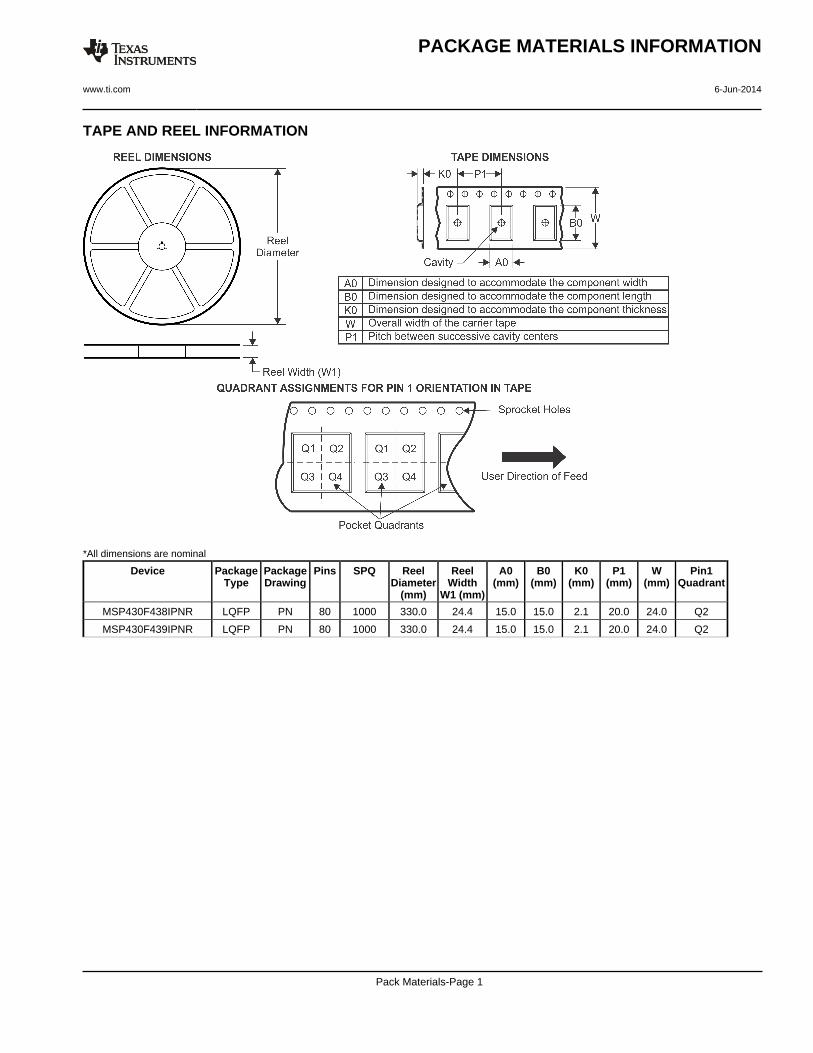
TAPE AND REEL INFORMATION
*All dimensions are nominal
Device PackageType
PackageDrawing
Pins SPQ ReelDiameter
(mm)
ReelWidth
W1 (mm)
A0(mm)
B0(mm)
K0(mm)
P1(mm)
W(mm)
Pin1Quadrant
MSP430F438IPNR LQFP PN 80 1000 330.0 24.4 15.0 15.0 2.1 20.0 24.0 Q2
MSP430F439IPNR LQFP PN 80 1000 330.0 24.4 15.0 15.0 2.1 20.0 24.0 Q2
PACKAGE MATERIALS INFORMATION
www.ti.com 6-Jun-2014
Pack Materials-Page 1
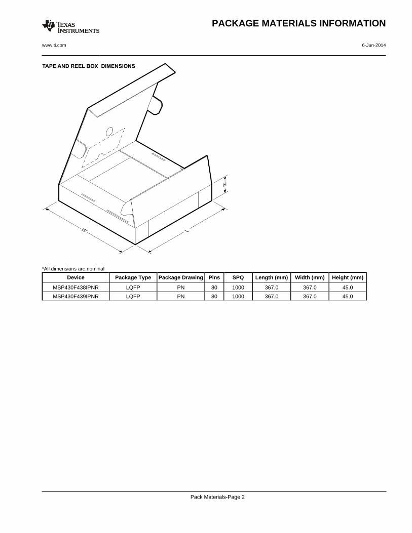
*All dimensions are nominal
Device Package Type Package Drawing Pins SPQ Length (mm) Width (mm) Height (mm)
MSP430F438IPNR LQFP PN 80 1000 367.0 367.0 45.0
MSP430F439IPNR LQFP PN 80 1000 367.0 367.0 45.0
PACKAGE MATERIALS INFORMATION
www.ti.com 6-Jun-2014
Pack Materials-Page 2
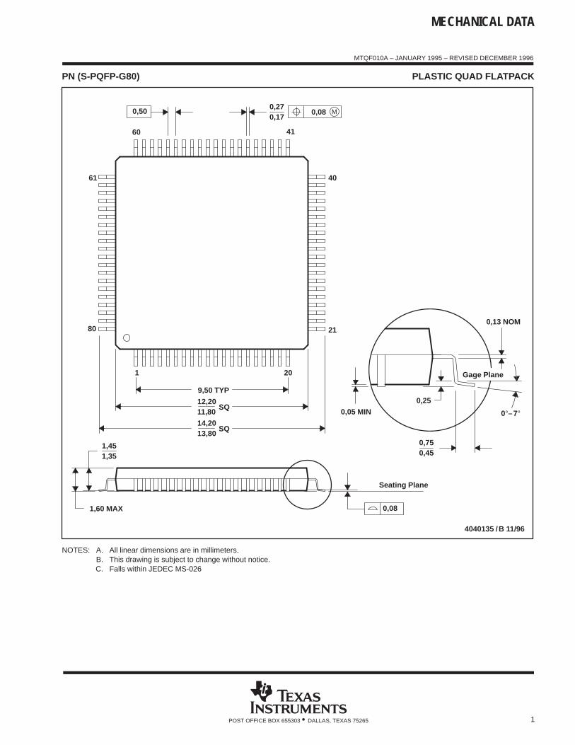
MECHANICAL DATA
MTQF010A – JANUARY 1995 – REVISED DECEMBER 1996
1POST OFFICE BOX 655303 • DALLAS, TEXAS 75265
PN (S-PQFP-G80) PLASTIC QUAD FLATPACK
4040135 /B 11/96
0,170,27
0,13 NOM
40
21
0,25
0,450,75
0,05 MIN
Seating Plane
Gage Plane
4160
61
80
20
SQ
SQ
1
13,8014,20
12,20
9,50 TYP
11,80
1,451,35
1,60 MAX 0,08
0,50 M0,08
0°–7°
NOTES: A. All linear dimensions are in millimeters.B. This drawing is subject to change without notice.C. Falls within JEDEC MS-026

IMPORTANT NOTICE AND DISCLAIMER
TI PROVIDES TECHNICAL AND RELIABILITY DATA (INCLUDING DATASHEETS), DESIGN RESOURCES (INCLUDING REFERENCE DESIGNS), APPLICATION OR OTHER DESIGN ADVICE, WEB TOOLS, SAFETY INFORMATION, AND OTHER RESOURCES “AS IS” AND WITH ALL FAULTS, AND DISCLAIMS ALL WARRANTIES, EXPRESS AND IMPLIED, INCLUDING WITHOUT LIMITATION ANY IMPLIED WARRANTIES OF MERCHANTABILITY, FITNESS FOR A PARTICULAR PURPOSE OR NON-INFRINGEMENT OF THIRD PARTY INTELLECTUAL PROPERTY RIGHTS.These resources are intended for skilled developers designing with TI products. You are solely responsible for (1) selecting the appropriate TI products for your application, (2) designing, validating and testing your application, and (3) ensuring your application meets applicable standards, and any other safety, security, or other requirements. These resources are subject to change without notice. TI grants you permission to use these resources only for development of an application that uses the TI products described in the resource. Other reproduction and display of these resources is prohibited. No license is granted to any other TI intellectual property right or to any third party intellectual property right. TI disclaims responsibility for, and you will fully indemnify TI and its representatives against, any claims, damages, costs, losses, and liabilities arising out of your use of these resources.TI’s products are provided subject to TI’s Terms of Sale (www.ti.com/legal/termsofsale.html) or other applicable terms available either on ti.com or provided in conjunction with such TI products. TI’s provision of these resources does not expand or otherwise alter TI’s applicable warranties or warranty disclaimers for TI products.
Mailing Address: Texas Instruments, Post Office Box 655303, Dallas, Texas 75265Copyright © 2020, Texas Instruments Incorporated