Embed Size (px)
Citation preview
MSP430F21x1
www.ti.com SLAS439F –SEPTEMBER 2004–REVISED AUGUST 2011
MIXED SIGNAL MICROCONTROLLER1FEATURES • Serial Onboard Programming, No External
Programming Voltage Needed, Programmable• Low Supply Voltage Range: 1.8 V to 3.6 VCode Protection by Security Fuse• Ultra-Low Power Consumption
• Bootstrap Loader– Active Mode: 250 μA at 1 MHz, 2.2 V• On Chip Emulation Module– Standby Mode: 0.7 μA• Family Members:– Off Mode (RAM Retention): 0.1 μA
– MSP430F2101• Ultra-Fast Wake-Up From Standby Mode in– 1KB + 256B Flash MemoryLess Than 1 μs– 128B RAM• 16-Bit RISC Architecture, 62.5-ns Instruction
– MSP430F2111Cycle Time– 2KB + 256B Flash Memory• Basic Clock Module Configurations– 128B RAM– Internal Frequencies up to 16 MHz With
Four Calibrated Frequencies to ±1% – MSP430F2121– 32-kHz Crystal – 4KB + 256B Flash Memory– High-Frequency Crystal up to 16 MHz – 256B RAM– Resonator – MSP430F2131– External Digital Clock Source – 8KB + 256B Flash Memory
• 16-Bit Timer_A With Three Capture/Compare – 256B RAMRegisters • Available in a 20-Pin Plastic Small-Outline
• On-Chip Comparator for Analog Signal Wide Body (SOWB) Package, 20-Pin PlasticCompare Function or Slope Analog-to-Digital Small-Outline Thin (TSSOP) Package, 20-Pin(A/D) Conversion TVSOP Package, and 24-Pin QFN Package
• Brownout Detector • For Complete Module Descriptions, See theMSP430x2xx Family User’s Guide (SLAU144)
DESCRIPTIONThe Texas Instruments MSP430 family of ultra-low-power microcontrollers consist of several devices featuringdifferent sets of peripherals targeted for various applications. The architecture, combined with five low-powermodes, is optimized to achieve extended battery life in portable measurement applications. The device features apowerful 16-bit RISC CPU, 16-bit registers, and constant generators that contribute to maximum codeefficiency.The digitally controlled oscillator (DCO) allows wake-up from low-power modes to active mode in lessthan 1 μs.
The MSP430x21x1 series is an ultra-low-power mixed signal microcontroller with a built-in 16-bit timer, versatileanalog comparator, and sixteen I/O pins.
Typical applications include sensor systems that capture analog signals, convert themto digital values, and thenprocess the data for display or for transmission to a host system. Stand-alone RF sensor front end is anotherarea of application. The analog comparator provides slope A/D conversion capability.
1
Please be aware that an important notice concerning availability, standard warranty, and use in critical applications of TexasInstruments semiconductor products and disclaimers thereto appears at the end of this data sheet.
PRODUCTION DATA information is current as of publication date. Copyright © 2004–2011, Texas Instruments IncorporatedProducts conform to specifications per the terms of the TexasInstruments standard warranty. Production processing does notnecessarily include testing of all parameters.
MSP430F21x1
SLAS439F –SEPTEMBER 2004–REVISED AUGUST 2011 www.ti.com
Table 1. Available Options
PACKAGED DEVICES
PLASTIC PLASTIC PLASTIC PLASTICTA20-PIN SOWB 20-PIN TSSOP 20-PIN TVSOP 24-PIN QFN
(DW) (PW) (DGV) (RGE)
MSP430F2101IDW MSP430F2101IPW MSP430F2101IDGV MSP430F2101IRGE
MSP430F2111IDW MSP430F2111IPW MSP430F2111IDGV MSP430F2111IRGE-40°C to 85°C
MSP430F2121IDW MSP430F2121IPW MSP430F2121IDGV MSP430F2121IRGE
MSP430F2131IDW MSP430F2131IPW MSP430F2131IDGV MSP430F2131IRGE
MSP430F2101TDW MSP430F2101TPW MSP430F2101TDGV MSP430F2101TRGE
MSP430F2111TDW MSP430F2111TPW MSP430F2111TDGV MSP430F2111TRGE-40°C to 105°C
MSP430F2121TDW MSP430F2121TPW MSP430F2121TDGV MSP430F2121TRGE
MSP430F2131TDW MSP430F2131TPW MSP430F2131TDGV MSP430F2131TRGE
Development Tool Support
All MSP430 microcontrollers include an Embedded Emulation Module (EEM) that allows advanced debuggingand programming through easy-to-use development tools. Recommended hardware options include:• Debugging and Programming Interface with Target Board
– MSP-FET430U28 (PW package)• Debugging and Programming Interface
– MSP-FET430UIF (USB)– MSP-FET430PIF (Parallel Port)
• Target Board– MSP-TS430PW28 (PW package)
• Production Programmer– MSP-GANG430
2 Copyright © 2004–2011, Texas Instruments Incorporated
1
2
3
4
5
6
7
8
9
10 11
12
13
14
15
16
17
18
19
20TEST
VCC
P2.5/CA5
VSS
XOUT/P2.7/CA7
XIN/P2.6/CA6
RST/NMI
P2.0/ACLK/CA2
P2.1/INCLK/CA3
P2.2/CAOUT/TA0/CA4
P1.7/TA2/TDO/TDI
P1.6/TA1/TDI/TCLK
P1.5/TA0/TMS
P1.4/SMCLK/TCK
P1.3/TA2
P1.2/TA1
P1.1/TA0
P1.0/TACLK
P2.4/TA2/CA1
P2.3/TA1/CA0
11
P2.4
/TA
2/C
A1
10
P2.3
/TA
1/C
A0
9
NC
8
P2.2
/CA
OU
T/T
A0/C
A4
7
P2.1
/IN
CLK
/CA
3
12
NC
5RST/NMI
4XIN/P2.6/CA6
3XOUT/P2.7/CA7
2VSS
1NC
6P2.0/ACLK/CA2
14 P1.1/TA0
15 P1.2/TA1
16 P1.3/TA2
17 P1.4/SMCLK/TCK
18 P1.5/TA0/TMS
13 P1.0/TACLK
20
P1.6
/TA
1/T
DI/T
CLK
21
P1.7
/TA
2/T
DO
/TD
I
22
TE
ST
23
VC
C
24
P2.5
/CA
5
19
NC
ExposedThermal Pad
MSP430F21x1
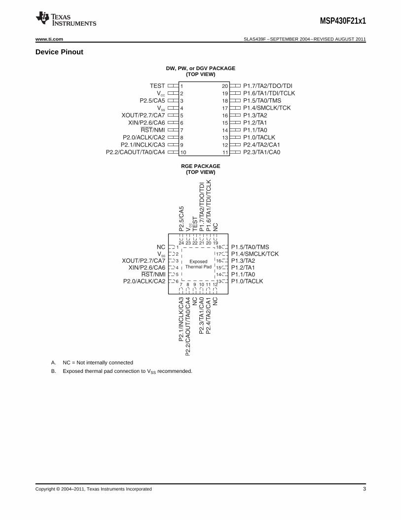
www.ti.com SLAS439F –SEPTEMBER 2004–REVISED AUGUST 2011
Device Pinout
DW, PW, or DGV PACKAGE(TOP VIEW)
RGE PACKAGE(TOP VIEW)
A. NC = Not internally connected
B. Exposed thermal pad connection to VSS recommended.
Copyright © 2004–2011, Texas Instruments Incorporated 3
Basic Clock
System+
RAM
256B
256B
128B
128B
Brownout
Protection
RST/NMI
VCC VSS
MCLK
SMCLK
Watchdog
WDT+
15/16 Bit
Timer_A3
3 CC
Registers
16MHz
CPU
incl. 16
Registers
Emulation
(2BP)
XOUT
JTAG
Interface
Flash
8kB
4kB
2kB
1kB
ACLK
XIN
Port P1
8 I/ O
Interrupt
capability,
pullup/down
resistors
Comparator
_A+
8 Channel
Input Mux
P1.x, JTAG
8
P2.x,XIN/XOUT
8
Port P2
8 I/ O
Interrupt
capability,
pullup/down
resistors
MDB
MAB
MSP430F21x1
SLAS439F –SEPTEMBER 2004–REVISED AUGUST 2011 www.ti.com
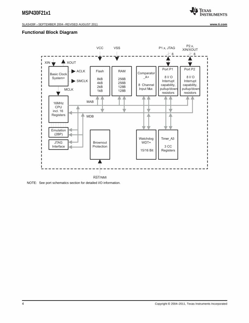
Functional Block Diagram
NOTE: See port schematics section for detailed I/O information.
4 Copyright © 2004–2011, Texas Instruments Incorporated
MSP430F21x1
www.ti.com SLAS439F –SEPTEMBER 2004–REVISED AUGUST 2011
Table 2. Terminal Functions
TERMINAL
NO.
DW, I/O DESCRIPTIONNAME PW, RGEor
DGV
General-purpose digital I/O pinP1.0/TACLK 13 13 I/O
Timer_A, clock signal TACLK input
General-purpose digital I/O pinP1.1/TA 14 14 I/O
Timer_A, capture: CCI0A input, compare: Out0 output/BSL transmit
General-purpose digital I/O pinP1.2/TA1 15 15 I/O
Timer_A, capture: CCI1A input, compare: Out1 output
General-purpose digital I/O pinP1.3/TA2 16 16 I/O
Timer_A, capture: CCI2A input, compare: Out2 output
General-purpose digital I/O pin / SMCLK signal outputP1.4/SMCLK/TCK 17 17 I/O
Test Clock input for device programming and test
General-purpose digital I/O pin / Timer_A, compare: Out0 outputP1.5/TA/TMS 18 18 I/O
Test Mode Select input for device programming and test
General-purpose digital I/O pin / Timer_A, compare: Out1 outputP1.6/TA1/TDI/TCLK 19 20 I/O
Test Data Input or Test Clock Input for programming and test
General-purpose digital I/O pin / Timer_A, compare: Out2 outputP1.7/TA2/TDO/TDI (1) 20 21 I/O
Test Data Output or Test Data Input for programming and test
General-purpose digital I/O pin / ACLK outputP2.0/ACLK/CA2 8 6 I/O
Comparator_A+, CA2 input
General-purpose digital I/O pin / Timer_A, clock signal at INCLKP2.1/INCLK/CA3 9 7 I/O
Comparator_A+, CA3 input
General-purpose digital I/O pin
P2.2/CAOUT/TA/CA4 10 8 I/O Timer_A, capture: CCI0B input/BSL receive
Comparator_A+, output / CA4 input
General-purpose digital I/O pin / Timer_A, compare: Out1 outputP2.3/CA0/TA1 11 10 I/O
Comparator_A+, CA0 input
General-purpose digital I/O pin / Timer_A, compare: Out2 outputP2.4/CA1/TA2 12 11 I/O
Comparator_A+, CA1 input
General-purpose digital I/O pinP2.5/CA5 3 24 I/O
Comparator_A+, CA5 input
Input terminal of crystal oscillator
XIN/P2.6/CA6 6 4 I/O General-purpose digital I/O pin
Comparator_A+, CA6 input
Output terminal of crystal oscillator
XOUT/P2.7/CA7 (2) 5 3 I/O General-purpose digital I/O pin
Comparator_A+, CA7 input
RST/NMI 7 5 I Reset or nonmaskable interrupt input
Selects test mode for JTAG pins on Port1. The device protection fuse is connected toTEST 1 22 I TEST.
VCC 2 23 Supply voltage
VSS 4 2 Ground reference
QFN Pad NA Pad NA QFN package thermal pad. Connect to VSS.
(1) TDO or TDI is selected via JTAG instruction.(2) If XOUT/P2.7/CA7 is used as an input, excess current will flow until P2SEL.7 is cleared. This is due to the oscillator output driver
connection to this pad after reset.
Copyright © 2004–2011, Texas Instruments Incorporated 5
General-Purpose Register
Program Counter
Stack Pointer
Status Register
Constant Generator
General-Purpose Register
General-Purpose Register
General-Purpose Register
PC/R0
SP/R1
SR/CG1/R2
CG2/R3
R4
R5
R12
R13
General-Purpose Register
General-Purpose Register
R6
R7
General-Purpose Register
General-Purpose Register
R8
R9
General-Purpose Register
General-Purpose Register
R10
R11
General-Purpose Register
General-Purpose Register
R14
R15
MSP430F21x1
SLAS439F –SEPTEMBER 2004–REVISED AUGUST 2011 www.ti.com
SHORT-FORM DESCRIPTION
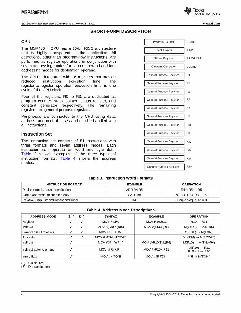
CPU
The MSP430™ CPU has a 16-bit RISC architecturethat is highly transparent to the application. Alloperations, other than program-flow instructions, areperformed as register operations in conjunction withseven addressing modes for source operand and fouraddressing modes for destination operand.
The CPU is integrated with 16 registers that providereduced instruction execution time. Theregister-to-register operation execution time is onecycle of the CPU clock.
Four of the registers, R0 to R3, are dedicated asprogram counter, stack pointer, status register, andconstant generator respectively. The remainingregisters are general-purpose registers.
Peripherals are connected to the CPU using data,address, and control buses and can be handled withall instructions.
Instruction Set
The instruction set consists of 51 instructions withthree formats and seven address modes. Eachinstruction can operate on word and byte data.Table 3 shows examples of the three types ofinstruction formats; Table 4 shows the addressmodes.
Table 3. Instruction Word Formats
INSTRUCTION FORMAT EXAMPLE OPERATION
Dual operands, source-destination ADD R4,R5 R4 + R5 → R5
Single operands, destination only CALL R8 PC → (TOS), R8 → PC
Relative jump, unconditional/conditional JNE Jump-on-equal bit = 0
Table 4. Address Mode Descriptions
ADDRESS MODE S (1) D (2) SYNTAX EXAMPLE OPERATION
Register MOV Rs,Rd MOV R10,R11 R10 → R11
Indexed MOV X(Rn),Y(Rm) MOV 2(R5),6(R6) M(2+R5) → M(6+R6)
Symbolic (PC relative) MOV EDE,TONI M(EDE) → M(TONI)
Absolute MOV &MEM,&TCDAT M(MEM) → M(TCDAT)
Indirect MOV @Rn,Y(Rm) MOV @R10,Tab(R6) M(R10) → M(Tab+R6)
M(R10) → R11Indirect autoincrement MOV @Rn+,Rm MOV @R10+,R11 R10 + 2 → R10
Immediate MOV #X,TONI MOV #45,TONI #45 → M(TONI)
(1) S = source(2) D = destination
6 Copyright © 2004–2011, Texas Instruments Incorporated
MSP430F21x1
www.ti.com SLAS439F –SEPTEMBER 2004–REVISED AUGUST 2011
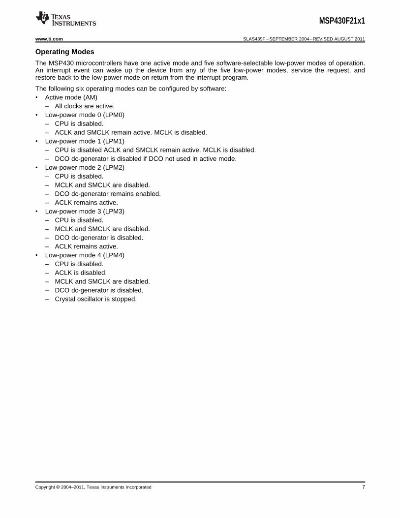
Operating Modes
The MSP430 microcontrollers have one active mode and five software-selectable low-power modes of operation.An interrupt event can wake up the device from any of the five low-power modes, service the request, andrestore back to the low-power mode on return from the interrupt program.
The following six operating modes can be configured by software:• Active mode (AM)
– All clocks are active.• Low-power mode 0 (LPM0)
– CPU is disabled.– ACLK and SMCLK remain active. MCLK is disabled.
• Low-power mode 1 (LPM1)– CPU is disabled ACLK and SMCLK remain active. MCLK is disabled.– DCO dc-generator is disabled if DCO not used in active mode.
• Low-power mode 2 (LPM2)– CPU is disabled.– MCLK and SMCLK are disabled.– DCO dc-generator remains enabled.– ACLK remains active.
• Low-power mode 3 (LPM3)– CPU is disabled.– MCLK and SMCLK are disabled.– DCO dc-generator is disabled.– ACLK remains active.
• Low-power mode 4 (LPM4)– CPU is disabled.– ACLK is disabled.– MCLK and SMCLK are disabled.– DCO dc-generator is disabled.– Crystal oscillator is stopped.
Copyright © 2004–2011, Texas Instruments Incorporated 7
MSP430F21x1
SLAS439F –SEPTEMBER 2004–REVISED AUGUST 2011 www.ti.com
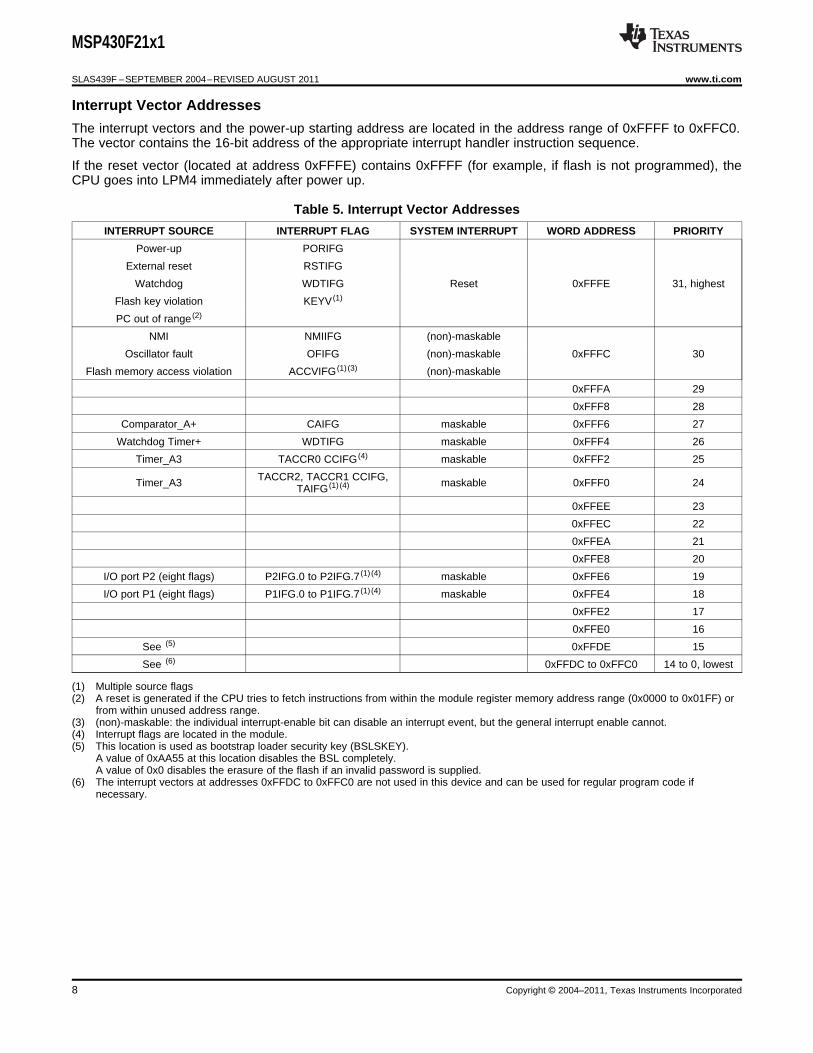
Interrupt Vector Addresses
The interrupt vectors and the power-up starting address are located in the address range of 0xFFFF to 0xFFC0.The vector contains the 16-bit address of the appropriate interrupt handler instruction sequence.
If the reset vector (located at address 0xFFFE) contains 0xFFFF (for example, if flash is not programmed), theCPU goes into LPM4 immediately after power up.
Table 5. Interrupt Vector Addresses
INTERRUPT SOURCE INTERRUPT FLAG SYSTEM INTERRUPT WORD ADDRESS PRIORITY
Power-up PORIFG
External reset RSTIFG
Watchdog WDTIFG Reset 0xFFFE 31, highest
Flash key violation KEYV (1)
PC out of range (2)
NMI NMIIFG (non)-maskable
Oscillator fault OFIFG (non)-maskable 0xFFFC 30
Flash memory access violation ACCVIFG (1) (3) (non)-maskable
0xFFFA 29
0xFFF8 28
Comparator_A+ CAIFG maskable 0xFFF6 27
Watchdog Timer+ WDTIFG maskable 0xFFF4 26
Timer_A3 TACCR0 CCIFG (4) maskable 0xFFF2 25
TACCR2, TACCR1 CCIFG,Timer_A3 maskable 0xFFF0 24TAIFG (1) (4)
0xFFEE 23
0xFFEC 22
0xFFEA 21
0xFFE8 20
I/O port P2 (eight flags) P2IFG.0 to P2IFG.7 (1) (4) maskable 0xFFE6 19
I/O port P1 (eight flags) P1IFG.0 to P1IFG.7 (1) (4) maskable 0xFFE4 18
0xFFE2 17
0xFFE0 16
See (5) 0xFFDE 15
See (6) 0xFFDC to 0xFFC0 14 to 0, lowest
(1) Multiple source flags(2) A reset is generated if the CPU tries to fetch instructions from within the module register memory address range (0x0000 to 0x01FF) or
from within unused address range.(3) (non)-maskable: the individual interrupt-enable bit can disable an interrupt event, but the general interrupt enable cannot.(4) Interrupt flags are located in the module.(5) This location is used as bootstrap loader security key (BSLSKEY).
A value of 0xAA55 at this location disables the BSL completely.A value of 0x0 disables the erasure of the flash if an invalid password is supplied.
(6) The interrupt vectors at addresses 0xFFDC to 0xFFC0 are not used in this device and can be used for regular program code ifnecessary.
8 Copyright © 2004–2011, Texas Instruments Incorporated
MSP430F21x1
www.ti.com SLAS439F –SEPTEMBER 2004–REVISED AUGUST 2011
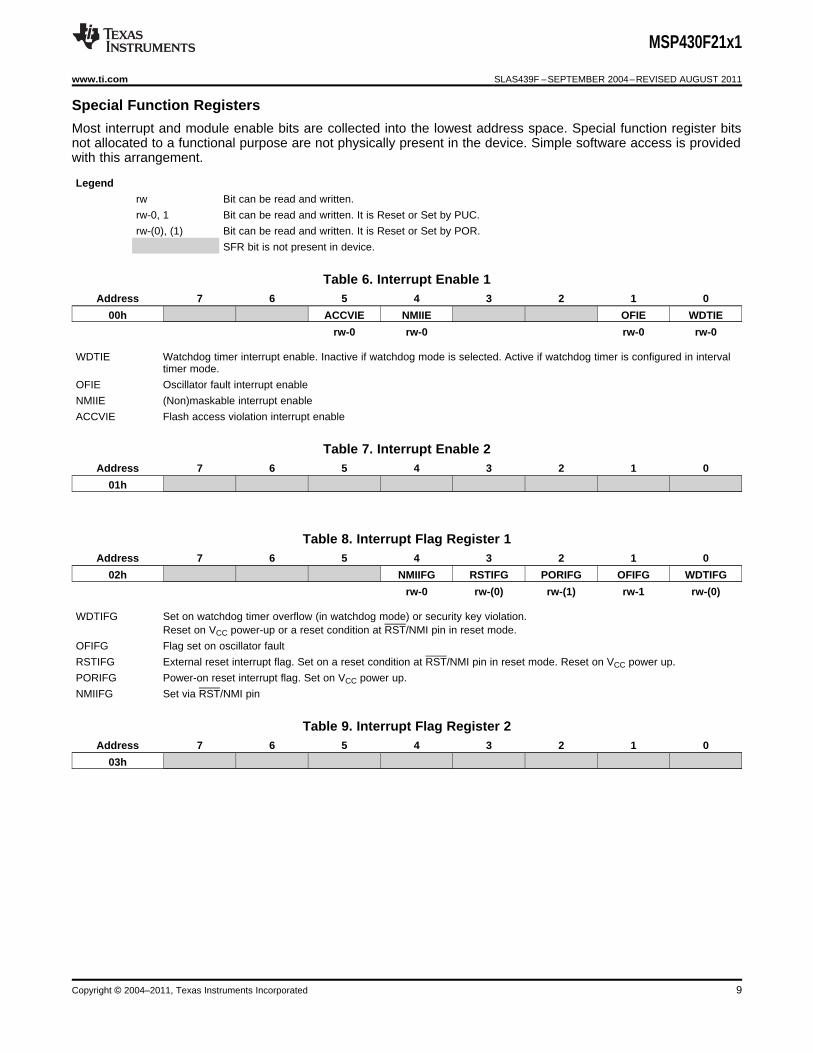
Special Function Registers
Most interrupt and module enable bits are collected into the lowest address space. Special function register bitsnot allocated to a functional purpose are not physically present in the device. Simple software access is providedwith this arrangement.
Legend
rw Bit can be read and written.
rw-0, 1 Bit can be read and written. It is Reset or Set by PUC.
rw-(0), (1) Bit can be read and written. It is Reset or Set by POR.
SFR bit is not present in device.
Table 6. Interrupt Enable 1Address 7 6 5 4 3 2 1 0
00h ACCVIE NMIIE OFIE WDTIE
rw-0 rw-0 rw-0 rw-0
WDTIE Watchdog timer interrupt enable. Inactive if watchdog mode is selected. Active if watchdog timer is configured in intervaltimer mode.
OFIE Oscillator fault interrupt enable
NMIIE (Non)maskable interrupt enable
ACCVIE Flash access violation interrupt enable
Table 7. Interrupt Enable 2Address 7 6 5 4 3 2 1 0
01h
Table 8. Interrupt Flag Register 1Address 7 6 5 4 3 2 1 0
02h NMIIFG RSTIFG PORIFG OFIFG WDTIFG
rw-0 rw-(0) rw-(1) rw-1 rw-(0)
WDTIFG Set on watchdog timer overflow (in watchdog mode) or security key violation.Reset on VCC power-up or a reset condition at RST/NMI pin in reset mode.
OFIFG Flag set on oscillator fault
RSTIFG External reset interrupt flag. Set on a reset condition at RST/NMI pin in reset mode. Reset on VCC power up.
PORIFG Power-on reset interrupt flag. Set on VCC power up.
NMIIFG Set via RST/NMI pin
Table 9. Interrupt Flag Register 2Address 7 6 5 4 3 2 1 0
03h
Copyright © 2004–2011, Texas Instruments Incorporated 9
MSP430F21x1
SLAS439F –SEPTEMBER 2004–REVISED AUGUST 2011 www.ti.com
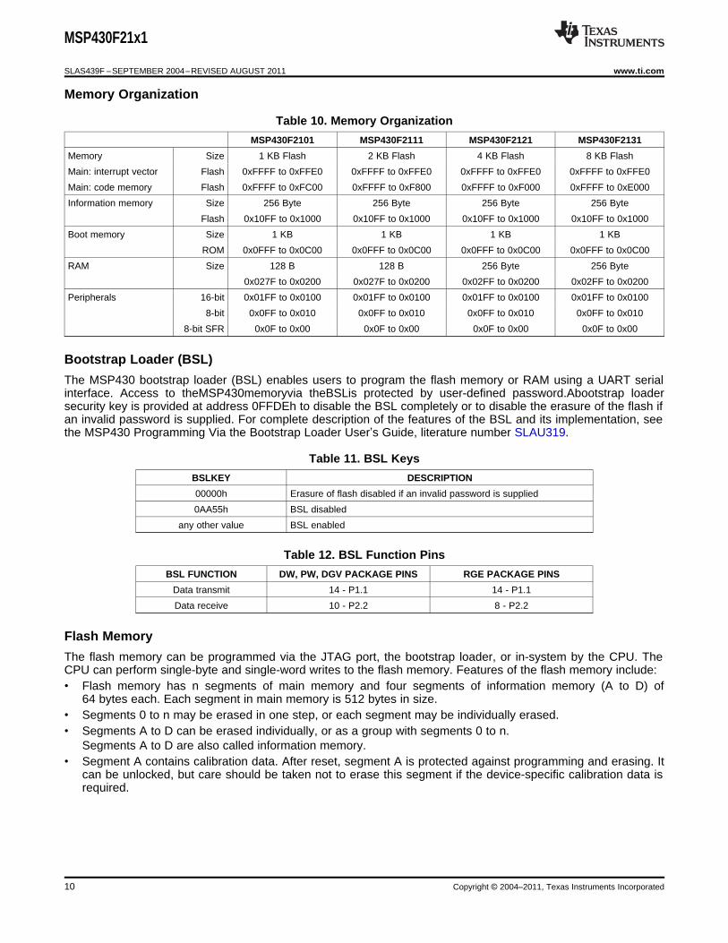
Memory Organization
Table 10. Memory Organization
MSP430F2101 MSP430F2111 MSP430F2121 MSP430F2131
Memory Size 1 KB Flash 2 KB Flash 4 KB Flash 8 KB Flash
Main: interrupt vector Flash 0xFFFF to 0xFFE0 0xFFFF to 0xFFE0 0xFFFF to 0xFFE0 0xFFFF to 0xFFE0
Main: code memory Flash 0xFFFF to 0xFC00 0xFFFF to 0xF800 0xFFFF to 0xF000 0xFFFF to 0xE000
Information memory Size 256 Byte 256 Byte 256 Byte 256 Byte
Flash 0x10FF to 0x1000 0x10FF to 0x1000 0x10FF to 0x1000 0x10FF to 0x1000
Boot memory Size 1 KB 1 KB 1 KB 1 KB
ROM 0x0FFF to 0x0C00 0x0FFF to 0x0C00 0x0FFF to 0x0C00 0x0FFF to 0x0C00
RAM Size 128 B 128 B 256 Byte 256 Byte
0x027F to 0x0200 0x027F to 0x0200 0x02FF to 0x0200 0x02FF to 0x0200
Peripherals 16-bit 0x01FF to 0x0100 0x01FF to 0x0100 0x01FF to 0x0100 0x01FF to 0x0100
8-bit 0x0FF to 0x010 0x0FF to 0x010 0x0FF to 0x010 0x0FF to 0x010
8-bit SFR 0x0F to 0x00 0x0F to 0x00 0x0F to 0x00 0x0F to 0x00
Bootstrap Loader (BSL)
The MSP430 bootstrap loader (BSL) enables users to program the flash memory or RAM using a UART serialinterface. Access to theMSP430memoryvia theBSLis protected by user-defined password.Abootstrap loadersecurity key is provided at address 0FFDEh to disable the BSL completely or to disable the erasure of the flash ifan invalid password is supplied. For complete description of the features of the BSL and its implementation, seethe MSP430 Programming Via the Bootstrap Loader User’s Guide, literature number SLAU319.
Table 11. BSL Keys
BSLKEY DESCRIPTION
00000h Erasure of flash disabled if an invalid password is supplied
0AA55h BSL disabled
any other value BSL enabled
Table 12. BSL Function Pins
BSL FUNCTION DW, PW, DGV PACKAGE PINS RGE PACKAGE PINS
Data transmit 14 - P1.1 14 - P1.1
Data receive 10 - P2.2 8 - P2.2
Flash Memory
The flash memory can be programmed via the JTAG port, the bootstrap loader, or in-system by the CPU. TheCPU can perform single-byte and single-word writes to the flash memory. Features of the flash memory include:• Flash memory has n segments of main memory and four segments of information memory (A to D) of
64 bytes each. Each segment in main memory is 512 bytes in size.• Segments 0 to n may be erased in one step, or each segment may be individually erased.• Segments A to D can be erased individually, or as a group with segments 0 to n.
Segments A to D are also called information memory.• Segment A contains calibration data. After reset, segment A is protected against programming and erasing. It
can be unlocked, but care should be taken not to erase this segment if the device-specific calibration data isrequired.
10 Copyright © 2004–2011, Texas Instruments Incorporated
MSP430F21x1
www.ti.com SLAS439F –SEPTEMBER 2004–REVISED AUGUST 2011
Peripherals
Peripherals are connected to the CPU through data, address, and control buses and can be handled using allinstructions. For complete module descriptions, see the MSP430x2xx Family User's Guide (SLAU144).
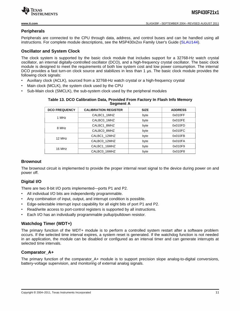
Oscillator and System Clock
The clock system is supported by the basic clock module that includes support for a 32768-Hz watch crystaloscillator, an internal digitally-controlled oscillator (DCO), and a high-frequency crystal oscillator. The basic clockmodule is designed to meet the requirements of both low system cost and low power consumption. The internalDCO provides a fast turn-on clock source and stabilizes in less than 1 µs. The basic clock module provides thefollowing clock signals:• Auxiliary clock (ACLK), sourced from a 32768-Hz watch crystal or a high-frequency crystal• Main clock (MCLK), the system clock used by the CPU• Sub-Main clock (SMCLK), the sub-system clock used by the peripheral modules
Table 13. DCO Calibration Data, Provided From Factory In Flash Info MemorySegment A
DCO FREQUENCY CALIBRATION REGISTER SIZE ADDRESS
CALBC1_1MHZ byte 0x010FF1 MHz
CALBC0_1MHZ byte 0x010FE
CALBC1_8MHZ byte 0x010FD8 MHz
CALBC0_8MHZ byte 0x010FC
CALBC1_12MHZ byte 0x010FB12 MHz
CALBC0_12MHZ byte 0x010FA
CALBC1_16MHZ byte 0x010F916 MHz
CALBC0_16MHZ byte 0x010F8
Brownout
The brownout circuit is implemented to provide the proper internal reset signal to the device during power on andpower off.
Digital I/O
There are two 8-bit I/O ports implemented—ports P1 and P2.• All individual I/O bits are independently programmable.• Any combination of input, output, and interrupt condition is possible.• Edge-selectable interrupt input capability for all eight bits of port P1 and P2.• Read/write access to port-control registers is supported by all instructions.• Each I/O has an individually programmable pullup/pulldown resistor.
Watchdog Timer (WDT+)
The primary function of the WDT+ module is to perform a controlled system restart after a software problemoccurs. If the selected time interval expires, a system reset is generated. If the watchdog function is not neededin an application, the module can be disabled or configured as an interval timer and can generate interrupts atselected time intervals.
Comparator_A+
The primary function of the comparator_A+ module is to support precision slope analog-to-digital conversions,battery-voltage supervision, and monitoring of external analog signals.
Copyright © 2004–2011, Texas Instruments Incorporated 11
MSP430F21x1
SLAS439F –SEPTEMBER 2004–REVISED AUGUST 2011 www.ti.com
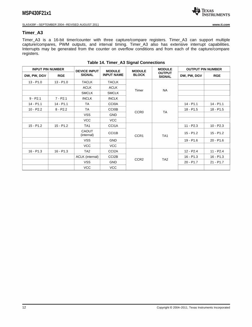
Timer_A3
Timer_A3 is a 16-bit timer/counter with three capture/compare registers. Timer_A3 can support multiplecapture/compares, PWM outputs, and interval timing. Timer_A3 also has extensive interrupt capabilities.Interrupts may be generated from the counter on overflow conditions and from each of the capture/compareregisters.
Table 14. Timer_A3 Signal Connections
INPUT PIN NUMBER MODULE OUTPUT PIN NUMBERDEVICE INPUT MODULE MODULE OUTPUTSIGNAL INPUT NAME BLOCKDW, PW, DGV RGE DW, PW, DGV RGESIGNAL
13 - P1.0 13 - P1.0 TACLK TACLK
ACLK ACLKTimer NA
SMCLK SMCLK
9 - P2.1 7 - P2.1 INCLK INCLK
14 - P1.1 14 - P1.1 TA CCI0A 14 - P1.1 14 - P1.1
10 - P2.2 8 - P2.2 TA CCI0B 18 - P1.5 18 - P1.5CCR0 TA
VSS GND
VCC VCC
15 - P1.2 15 - P1.2 TA1 CCI1A 11 - P2.3 10 - P2.3
CAOUT CCI1B 15 - P1.2 15 - P1.2(internal) CCR1 TA1VSS GND 19 - P1.6 20 - P1.6
VCC VCC
16 - P1.3 16 - P1.3 TA2 CCI2A 12 - P2.4 11 - P2.4
ACLK (internal) CCI2B 16 - P1.3 16 - P1.3CCR2 TA2
VSS GND 20 - P1.7 21 - P1.7
VCC VCC
12 Copyright © 2004–2011, Texas Instruments Incorporated
MSP430F21x1
www.ti.com SLAS439F –SEPTEMBER 2004–REVISED AUGUST 2011
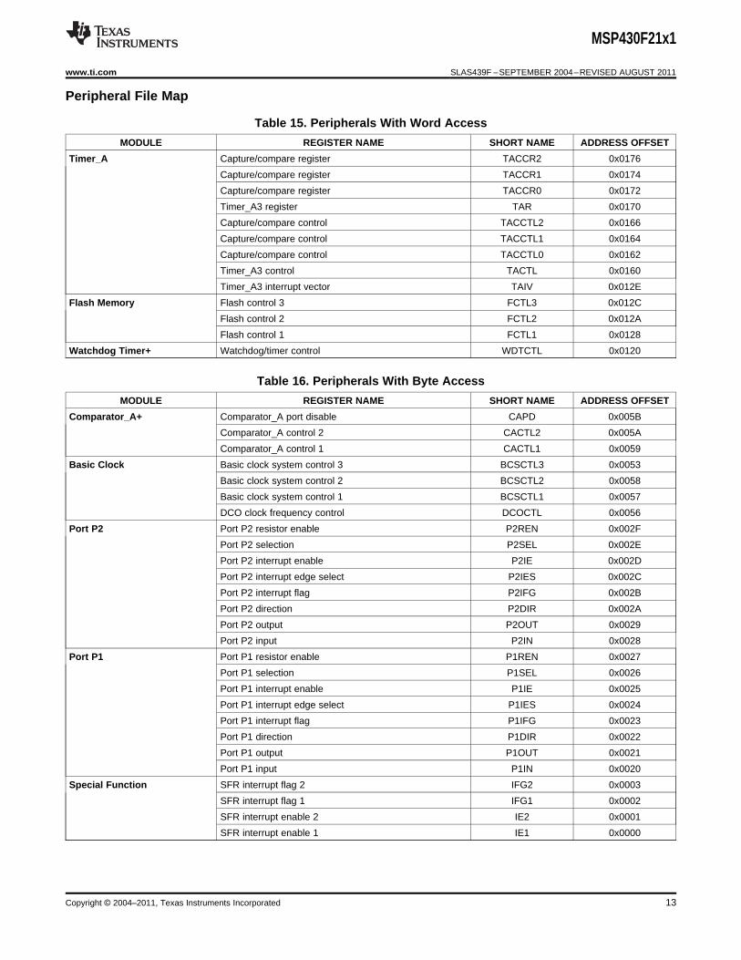
Peripheral File Map
Table 15. Peripherals With Word Access
MODULE REGISTER NAME SHORT NAME ADDRESS OFFSET
Timer_A Capture/compare register TACCR2 0x0176
Capture/compare register TACCR1 0x0174
Capture/compare register TACCR0 0x0172
Timer_A3 register TAR 0x0170
Capture/compare control TACCTL2 0x0166
Capture/compare control TACCTL1 0x0164
Capture/compare control TACCTL0 0x0162
Timer_A3 control TACTL 0x0160
Timer_A3 interrupt vector TAIV 0x012E
Flash Memory Flash control 3 FCTL3 0x012C
Flash control 2 FCTL2 0x012A
Flash control 1 FCTL1 0x0128
Watchdog Timer+ Watchdog/timer control WDTCTL 0x0120
Table 16. Peripherals With Byte Access
MODULE REGISTER NAME SHORT NAME ADDRESS OFFSET
Comparator_A+ Comparator_A port disable CAPD 0x005B
Comparator_A control 2 CACTL2 0x005A
Comparator_A control 1 CACTL1 0x0059
Basic Clock Basic clock system control 3 BCSCTL3 0x0053
Basic clock system control 2 BCSCTL2 0x0058
Basic clock system control 1 BCSCTL1 0x0057
DCO clock frequency control DCOCTL 0x0056
Port P2 Port P2 resistor enable P2REN 0x002F
Port P2 selection P2SEL 0x002E
Port P2 interrupt enable P2IE 0x002D
Port P2 interrupt edge select P2IES 0x002C
Port P2 interrupt flag P2IFG 0x002B
Port P2 direction P2DIR 0x002A
Port P2 output P2OUT 0x0029
Port P2 input P2IN 0x0028
Port P1 Port P1 resistor enable P1REN 0x0027
Port P1 selection P1SEL 0x0026
Port P1 interrupt enable P1IE 0x0025
Port P1 interrupt edge select P1IES 0x0024
Port P1 interrupt flag P1IFG 0x0023
Port P1 direction P1DIR 0x0022
Port P1 output P1OUT 0x0021
Port P1 input P1IN 0x0020
Special Function SFR interrupt flag 2 IFG2 0x0003
SFR interrupt flag 1 IFG1 0x0002
SFR interrupt enable 2 IE2 0x0001
SFR interrupt enable 1 IE1 0x0000
Copyright © 2004–2011, Texas Instruments Incorporated 13
6 MHz
12 MHz
16 MHz
1.8 V 2.2 V 2.7 V 3.3 V 3.6 V
Supply Voltage − V
Syste
mF
reque
ncy
−M
Hz
Supply voltage range
during flash memory
programming
Supply voltage range
during program execution
Legend :
MSP430F21x1
SLAS439F –SEPTEMBER 2004–REVISED AUGUST 2011 www.ti.com
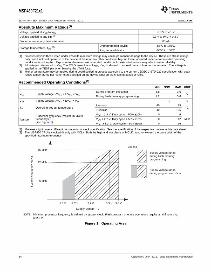
Absolute Maximum Ratings (1)
Voltage applied at VCC to VSS -0.3 V to 4.1 V
Voltage applied to any pin (2) -0.3 V to (VCC + 0.3 V)
Diode current at any device terminal ±2 mA
Unprogrammed device -55°C to 150°CStorage temperature, Tstg
(3)
Programmed device -55°C to 150°C
(1) Stresses beyond those listed under absolute maximum ratings may cause permanent damage to the device. These are stress ratingsonly, and functional operation of the device at these or any other conditions beyond those indicated under recommended operatingconditions is not implied. Exposure to absolute-maximum-rated conditions for extended periods may affect device reliability.
(2) All voltages referenced to VSS. The JTAG fuse-blow voltage, VFB, is allowed to exceed the absolute maximum rating. The voltage isapplied to the TEST pin when blowing the JTAG fuse.
(3) Higher temperature may be applied during board soldering process according to the current JEDEC J-STD-020 specification with peakreflow temperatures not higher than classified on the device label on the shipping boxes or reels.
Recommended Operating Conditions (1)
MIN NOM MAX UNIT
During program execution 1.8 3.6VCC Supply voltage, AVCC = DVCC = VCC V
During flash memory programming 2.2 3.6
VSS Supply voltage, AVSS = DVSS = VSS 0 V
I version -40 85TA Operating free-air temperature °C
T version -40 105
VCC = 1.8 V, Duty cycle = 50% ±10% 0 6Processor frequency (maximum MCLKfSYSTEM frequency) (2) (1) VCC = 2.7 V, Duty cycle = 50% ±10% 0 12 MHz
(see Figure 1) VCC ≥ 3.3 V, Duty cycle = 50% ±10% 0 16
(1) Modules might have a different maximum input clock specification. See the specification of the respective module in this data sheet.(2) The MSP430 CPU is clocked directly with MCLK. Both the high and low phase of MCLK must not exceed the pulse width of the
specified maximum frequency.
NOTE: Minimum processor frequency is defined by system clock. Flash program or erase operations require a minimum VCCof 2.2 V.
Figure 1. Operating Area
14 Copyright © 2004–2011, Texas Instruments Incorporated
0.0
1.0
2.0
3.0
4.0
5.0
0
f – DCO Frequency – MHzDCO
Active
ModeC
urr
ent–
mA
V = 3 VCC
4 8 12 16
V = 2.2 VCC
T = 85°CA
T = 25°CA
T = 85°CA
T = 25°CA
0.0
1.0
2.0
3.0
4.0
5.0
6.0
7.0
1.5
V – Supply Voltage – VCC
Active
Mode C
urr
ent–
mA
f = 16 MHzDCO
f = 12 MHzDCO
f = 8 MHzDCO
f = 1 MHzDCO
2.0 2.5 3.0 3.5 4.0
MSP430F21x1
www.ti.com SLAS439F –SEPTEMBER 2004–REVISED AUGUST 2011
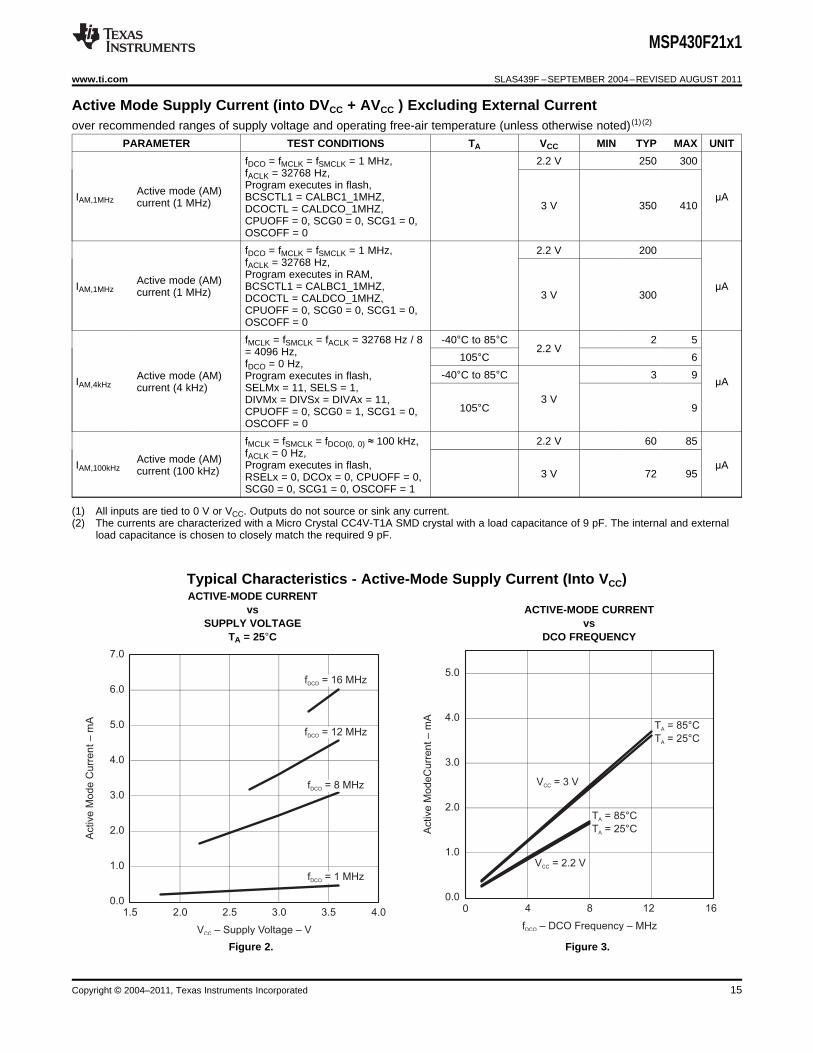
Active Mode Supply Current (into DVCC + AVCC ) Excluding External Currentover recommended ranges of supply voltage and operating free-air temperature (unless otherwise noted) (1) (2)
PARAMETER TEST CONDITIONS TA VCC MIN TYP MAX UNIT
fDCO = fMCLK = fSMCLK = 1 MHz, 2.2 V 250 300fACLK = 32768 Hz,Program executes in flash,Active mode (AM)IAM,1MHz BCSCTL1 = CALBC1_1MHZ, µAcurrent (1 MHz) 3 V 350 410DCOCTL = CALDCO_1MHZ,CPUOFF = 0, SCG0 = 0, SCG1 = 0,OSCOFF = 0
fDCO = fMCLK = fSMCLK = 1 MHz, 2.2 V 200fACLK = 32768 Hz,Program executes in RAM,Active mode (AM)IAM,1MHz BCSCTL1 = CALBC1_1MHZ, µAcurrent (1 MHz) 3 V 300DCOCTL = CALDCO_1MHZ,CPUOFF = 0, SCG0 = 0, SCG1 = 0,OSCOFF = 0
fMCLK = fSMCLK = fACLK = 32768 Hz / 8 -40°C to 85°C 2 52.2 V= 4096 Hz, 105°C 6
fDCO = 0 Hz,-40°C to 85°C 3 9Active mode (AM) Program executes in flash,IAM,4kHz µAcurrent (4 kHz) SELMx = 11, SELS = 1,
3 VDIVMx = DIVSx = DIVAx = 11,105°C 9CPUOFF = 0, SCG0 = 1, SCG1 = 0,
OSCOFF = 0
fMCLK = fSMCLK = fDCO(0, 0) ≈ 100 kHz, 2.2 V 60 85fACLK = 0 Hz,Active mode (AM)IAM,100kHz Program executes in flash, µAcurrent (100 kHz) 3 V 72 95RSELx = 0, DCOx = 0, CPUOFF = 0,SCG0 = 0, SCG1 = 0, OSCOFF = 1
(1) All inputs are tied to 0 V or VCC. Outputs do not source or sink any current.(2) The currents are characterized with a Micro Crystal CC4V-T1A SMD crystal with a load capacitance of 9 pF. The internal and external
load capacitance is chosen to closely match the required 9 pF.
Typical Characteristics - Active-Mode Supply Current (Into VCC)ACTIVE-MODE CURRENT
vs ACTIVE-MODE CURRENTSUPPLY VOLTAGE vs
TA = 25°C DCO FREQUENCY
Figure 2. Figure 3.
Copyright © 2004–2011, Texas Instruments Incorporated 15
MSP430F21x1
SLAS439F –SEPTEMBER 2004–REVISED AUGUST 2011 www.ti.com
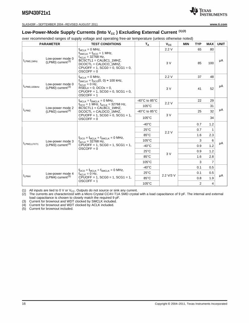
Low-Power-Mode Supply Currents (Into VCC ) Excluding External Current (1) (2)
over recommended ranges of supply voltage and operating free-air temperature (unless otherwise noted)
PARAMETER TEST CONDITIONS TA VCC MIN TYP MAX UNIT
fMCLK = 0 MHz, 2.2 V 65 80fSMCLK = fDCO = 1 MHz,fACLK = 32768 Hz,Low-power mode 0ILPM0,1MHz BCSCTL1 = CALBC1_1MHZ, µA(LPM0) current (3)
3 V 85 100DCOCTL = CALDCO_1MHZ,CPUOFF = 1, SCG0 = 0, SCG1 = 0,OSCOFF = 0
fMCLK = 0 MHz, 2.2 V 37 48fSMCLK = fDCO(0, 0) ≈ 100 kHz,
Low-power mode 0 fACLK = 0 Hz,ILPM0,100kHz µA(LPM0) current (3) RSELx = 0, DCOx = 0, 3 V 41 52CPUOFF = 1, SCG0 = 0, SCG1 = 0,OSCOFF = 1
fMCLK = fSMCLK = 0 MHz, -40°C to 85°C 22 292.2 VfDCO = 1 MHz, fACLK = 32768 Hz, 105°C 31
Low-power mode 2 BCSCTL1 = CALBC1_1MHZ,ILPM2 µA-40°C to 85°C 25 32(LPM2) current (4) DCOCTL = CALDCO_1MHZ,3 VCPUOFF = 1, SCG0 = 0, SCG1 = 1,
105°C 34OSCOFF = 0
-40°C 0.7 1.2
25°C 0.7 12.2 V
85°C 1.6 2.3fDCO = fMCLK = fSMCLK = 0 MHz,
105°C 3 6Low-power mode 3 fACLK = 32768 Hz,ILPM3,LFXT1 µA(LPM3) current (4) CPUOFF = 1, SCG0 = 1, SCG1 = 1, -40°C 0.9 1.2OSCOFF = 0
25°C 0.9 1.23 V
85°C 1.6 2.8
105°C 3 7
-40°C 0.1 0.5fDCO = fMCLK = fSMCLK = 0 MHz,
25°C 0.1 0.5Low-power mode 4 fACLK = 0 Hz,ILPM4 2.2 V/3 V µA(LPM4) current (5) CPUOFF = 1, SCG0 = 1, SCG1 = 1, 85°C 0.8 1.9OSCOFF = 1
105°C 2 4
(1) All inputs are tied to 0 V or VCC. Outputs do not source or sink any current.(2) The currents are characterized with a Micro Crystal CC4V-T1A SMD crystal with a load capacitance of 9 pF. The internal and external
load capacitance is chosen to closely match the required 9 pF.(3) Current for brownout and WDT clocked by SMCLK included.(4) Current for brownout and WDT clocked by ACLK included.(5) Current for brownout included.
16 Copyright © 2004–2011, Texas Instruments Incorporated
MSP430F21x1
www.ti.com SLAS439F –SEPTEMBER 2004–REVISED AUGUST 2011
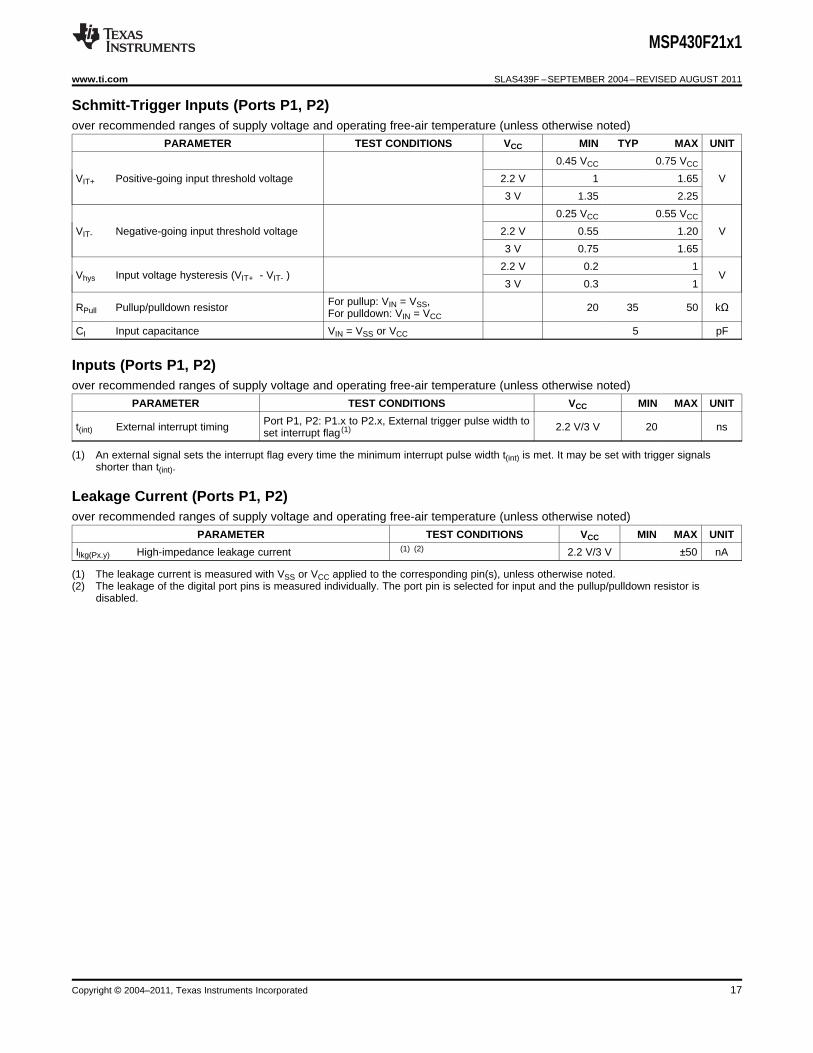
Schmitt-Trigger Inputs (Ports P1, P2)over recommended ranges of supply voltage and operating free-air temperature (unless otherwise noted)
PARAMETER TEST CONDITIONS VCC MIN TYP MAX UNIT
0.45 VCC 0.75 VCC
VIT+ Positive-going input threshold voltage 2.2 V 1 1.65 V
3 V 1.35 2.25
0.25 VCC 0.55 VCC
VIT- Negative-going input threshold voltage 2.2 V 0.55 1.20 V
3 V 0.75 1.65
2.2 V 0.2 1Vhys Input voltage hysteresis (VIT+ - VIT- ) V
3 V 0.3 1
For pullup: VIN = VSS,RPull Pullup/pulldown resistor 20 35 50 kΩFor pulldown: VIN = VCC
CI Input capacitance VIN = VSS or VCC 5 pF
Inputs (Ports P1, P2)over recommended ranges of supply voltage and operating free-air temperature (unless otherwise noted)
PARAMETER TEST CONDITIONS VCC MIN MAX UNIT
Port P1, P2: P1.x to P2.x, External trigger pulse width tot(int) External interrupt timing 2.2 V/3 V 20 nsset interrupt flag (1)
(1) An external signal sets the interrupt flag every time the minimum interrupt pulse width t(int) is met. It may be set with trigger signalsshorter than t(int).
Leakage Current (Ports P1, P2)over recommended ranges of supply voltage and operating free-air temperature (unless otherwise noted)
PARAMETER TEST CONDITIONS VCC MIN MAX UNIT
Ilkg(Px.y) High-impedance leakage current (1) (2) 2.2 V/3 V ±50 nA
(1) The leakage current is measured with VSS or VCC applied to the corresponding pin(s), unless otherwise noted.(2) The leakage of the digital port pins is measured individually. The port pin is selected for input and the pullup/pulldown resistor is
disabled.
Copyright © 2004–2011, Texas Instruments Incorporated 17
MSP430F21x1
SLAS439F –SEPTEMBER 2004–REVISED AUGUST 2011 www.ti.com
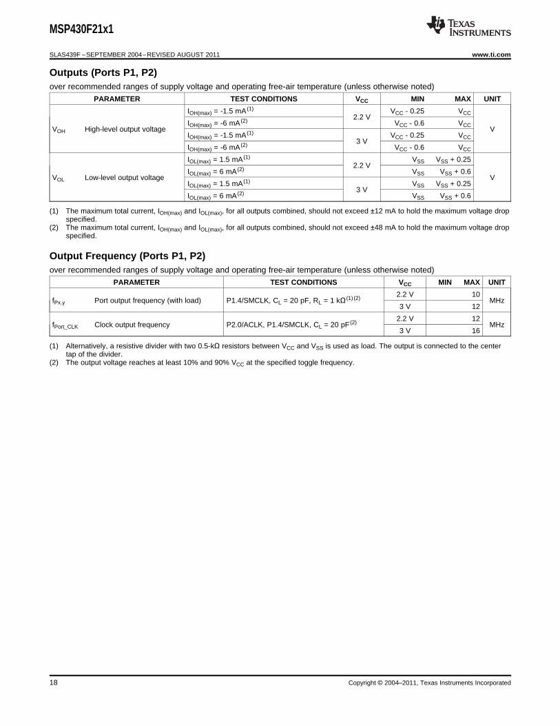
Outputs (Ports P1, P2)over recommended ranges of supply voltage and operating free-air temperature (unless otherwise noted)
PARAMETER TEST CONDITIONS VCC MIN MAX UNIT
IOH(max) = -1.5 mA (1) VCC - 0.25 VCC2.2 V
IOH(max) = -6 mA (2) VCC - 0.6 VCCVOH High-level output voltage V
IOH(max) = -1.5 mA (1) VCC - 0.25 VCC3 V
IOH(max) = -6 mA (2) VCC - 0.6 VCC
IOL(max) = 1.5 mA (1) VSS VSS + 0.252.2 V
IOL(max) = 6 mA (2) VSS VSS + 0.6VOL Low-level output voltage V
IOL(max) = 1.5 mA (1) VSS VSS + 0.253 V
IOL(max) = 6 mA (2) VSS VSS + 0.6
(1) The maximum total current, IOH(max) and IOL(max), for all outputs combined, should not exceed ±12 mA to hold the maximum voltage dropspecified.
(2) The maximum total current, IOH(max) and IOL(max), for all outputs combined, should not exceed ±48 mA to hold the maximum voltage dropspecified.
Output Frequency (Ports P1, P2)over recommended ranges of supply voltage and operating free-air temperature (unless otherwise noted)
PARAMETER TEST CONDITIONS VCC MIN MAX UNIT
2.2 V 10fPx.y Port output frequency (with load) P1.4/SMCLK, CL = 20 pF, RL = 1 kΩ (1) (2) MHz
3 V 12
2.2 V 12fPort_CLK Clock output frequency P2.0/ACLK, P1.4/SMCLK, CL = 20 pF (2) MHz
3 V 16
(1) Alternatively, a resistive divider with two 0.5-kΩ resistors between VCC and VSS is used as load. The output is connected to the centertap of the divider.
(2) The output voltage reaches at least 10% and 90% VCC at the specified toggle frequency.
18 Copyright © 2004–2011, Texas Instruments Incorporated
VOL − Low-Level Output Voltage − V
0.0
5.0
10.0
15.0
20.0
25.0
0.0 0.5 1.0 1.5 2.0 2.5
VCC = 2.2 V
P2.4
TA = 25°C
TA = 85°C
OL
I−
Typic
al Low
-Level O
utp
ut C
urr
ent
−m
A
VOL − Low-Level Output Voltage − V
0.0
10.0
20.0
30.0
40.0
50.0
0.0 0.5 1.0 1.5 2.0 2.5 3.0 3.5
VCC = 3 V
P2.4 TA = 25°C
TA = 85°C
OL
I−
Typic
al Low
-Level O
utp
ut C
urr
ent
−m
A
VOH − High-Level Output Voltage − V
−25.0
−20.0
−15.0
−10.0
−5.0
0.0
0.0 0.5 1.0 1.5 2.0 2.5
VCC = 2.2 V
P2.4
TA = 25°C
TA = 85°C
OH
I−
Typic
al H
igh-L
evel O
utp
ut C
urr
ent
−m
A
VOH − High-Level Output Voltage − V
−50.0
−40.0
−30.0
−20.0
−10.0
0.0
0.0 0.5 1.0 1.5 2.0 2.5 3.0 3.5
VCC = 3 V
P2.4
TA = 25°C
TA = 85°C
OH
I−
Typic
al H
igh-L
evel O
utp
ut C
urr
ent
−m
A
MSP430F21x1
www.ti.com SLAS439F –SEPTEMBER 2004–REVISED AUGUST 2011
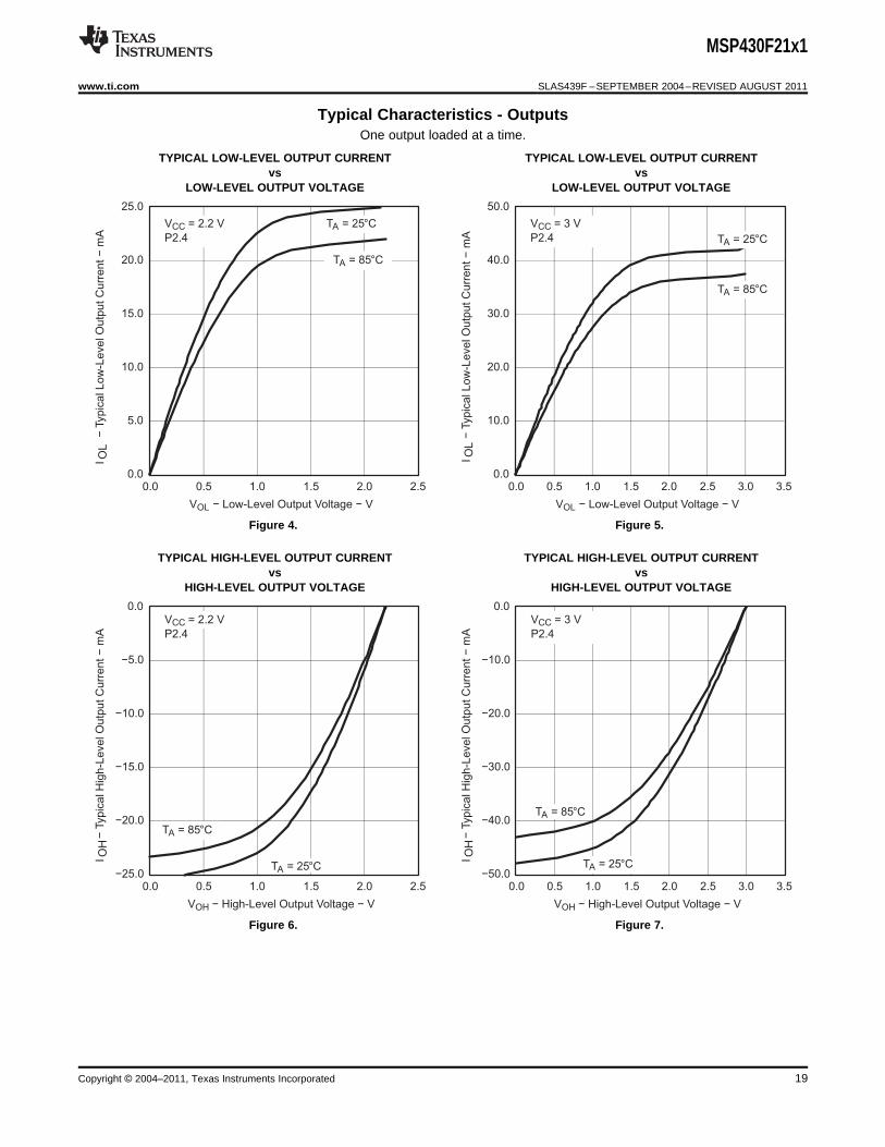
Typical Characteristics - OutputsOne output loaded at a time.
TYPICAL LOW-LEVEL OUTPUT CURRENT TYPICAL LOW-LEVEL OUTPUT CURRENTvs vs
LOW-LEVEL OUTPUT VOLTAGE LOW-LEVEL OUTPUT VOLTAGE
Figure 4. Figure 5.
TYPICAL HIGH-LEVEL OUTPUT CURRENT TYPICAL HIGH-LEVEL OUTPUT CURRENTvs vs
HIGH-LEVEL OUTPUT VOLTAGE HIGH-LEVEL OUTPUT VOLTAGE
Figure 6. Figure 7.
Copyright © 2004–2011, Texas Instruments Incorporated 19
0
1
t d(BOR)
VCC
V(B_IT−)
Vhys(B_IT−)
VCC(start)
MSP430F21x1
SLAS439F –SEPTEMBER 2004–REVISED AUGUST 2011 www.ti.com
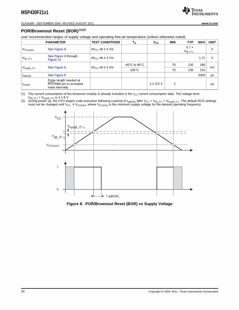
POR/Brownout Reset (BOR) (1) (2)
over recommended ranges of supply voltage and operating free-air temperature (unless otherwise noted)
PARAMETER TEST CONDITIONS TA VCC MIN TYP MAX UNIT
0.7 ×VCC(start) See Figure 8 dVCC /dt ≤ 3 V/s VV(B_IT-)
See Figure 8 throughV(B_IT-) dVCC /dt ≤ 3 V/s 1.71 VFigure 10
-40°C to 85°C 70 130 180Vhys(B_IT-) See Figure 8 dVCC /dt ≤ 3 V/s mV
105°C 70 130 210
td(BOR) See Figure 8 2000 µs
Pulse length needed att(reset) RST/NMI pin to accepted 2.2 V/3 V 2 µs
reset internally
(1) The current consumption of the brownout module is already included in the ICC current consumption data. The voltage levelV(B_IT-) + Vhys(B_IT-) is ≤ 1.8 V.
(2) During power up, the CPU begins code execution following a period of td(BOR) after VCC = V(B_IT-) + Vhys(B_IT-). The default DCO settingsmust not be changed until VCC ≥ VCC(min), where VCC(min) is the minimum supply voltage for the desired operating frequency.
Figure 8. POR/Brownout Reset (BOR) vs Supply Voltage
20 Copyright © 2004–2011, Texas Instruments Incorporated
VCC(drop)
VCC
3 V
t pw
0
0.5
1
1.5
2
0.001 1 1000
Typical Conditions
1 ns 1 nstpw − Pulse Width − µs
VC
C(d
rop)
−V
tpw − Pulse Width − µs
VCC = 3 V
VCC
0
0.5
1
1.5
2
VCC(drop)
t pw
tpw − Pulse Width − µs
VC
C(d
rop)
−V
3 V
0.001 1 1000 tf tr
tpw − Pulse Width − µs
tf = tr
Typical Conditions
VCC = 3 V
MSP430F21x1
www.ti.com SLAS439F –SEPTEMBER 2004–REVISED AUGUST 2011
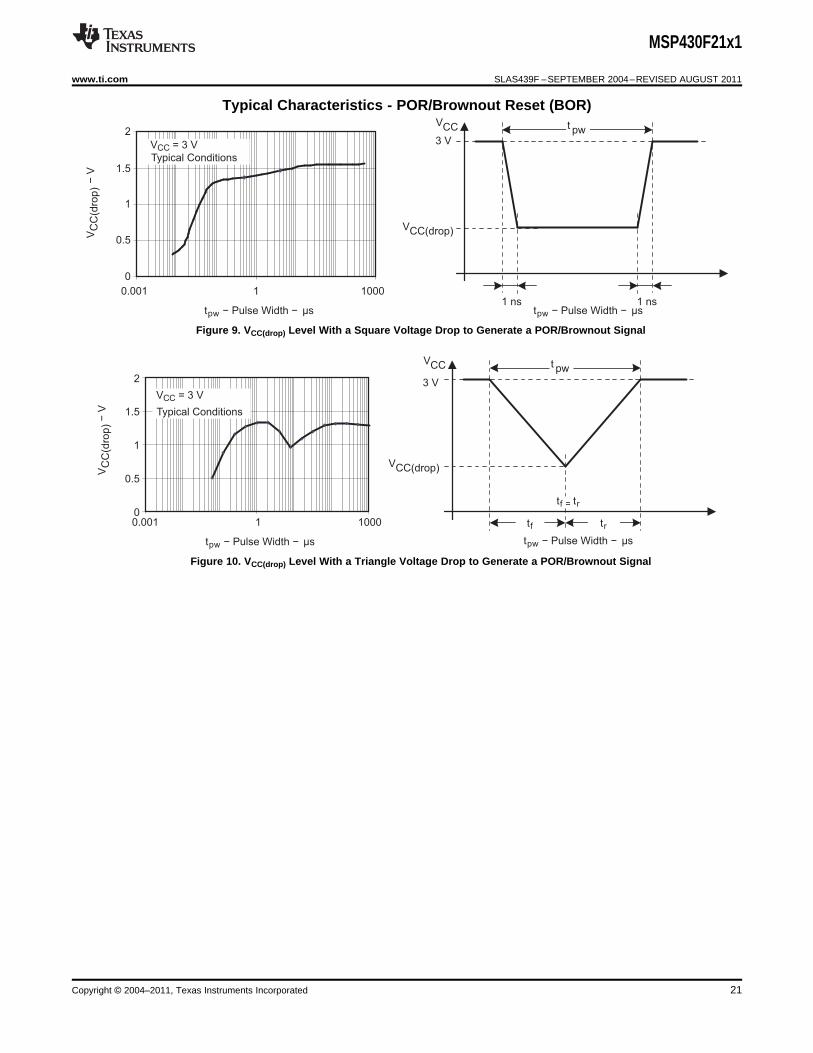
Typical Characteristics - POR/Brownout Reset (BOR)
Figure 9. VCC(drop) Level With a Square Voltage Drop to Generate a POR/Brownout Signal
Figure 10. VCC(drop) Level With a Triangle Voltage Drop to Generate a POR/Brownout Signal
Copyright © 2004–2011, Texas Instruments Incorporated 21
DCO(RSEL,DCO) DCO(RSEL,DCO+1)average
DCO(RSEL,DCO) DCO(RSEL,DCO+1)
32 × f × ff =
MOD × f + (32 – MOD) × f
MSP430F21x1
SLAS439F –SEPTEMBER 2004–REVISED AUGUST 2011 www.ti.com
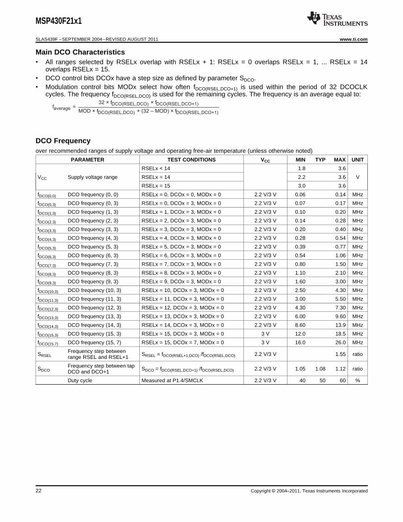
Main DCO Characteristics• All ranges selected by RSELx overlap with RSELx + 1: RSELx = 0 overlaps RSELx = 1, ... RSELx = 14
overlaps RSELx = 15.• DCO control bits DCOx have a step size as defined by parameter SDCO.• Modulation control bits MODx select how often fDCO(RSEL,DCO+1) is used within the period of 32 DCOCLK
cycles. The frequency fDCO(RSEL,DCO) is used for the remaining cycles. The frequency is an average equal to:
DCO Frequencyover recommended ranges of supply voltage and operating free-air temperature (unless otherwise noted)
PARAMETER TEST CONDITIONS VCC MIN TYP MAX UNIT
RSELx < 14 1.8 3.6
VCC Supply voltage range RSELx = 14 2.2 3.6 V
RSELx = 15 3.0 3.6
fDCO(0,0) DCO frequency (0, 0) RSELx = 0, DCOx = 0, MODx = 0 2.2 V/3 V 0.06 0.14 MHz
fDCO(0,3) DCO frequency (0, 3) RSELx = 0, DCOx = 3, MODx = 0 2.2 V/3 V 0.07 0.17 MHz
fDCO(1,3) DCO frequency (1, 3) RSELx = 1, DCOx = 3, MODx = 0 2.2 V/3 V 0.10 0.20 MHz
fDCO(2,3) DCO frequency (2, 3) RSELx = 2, DCOx = 3, MODx = 0 2.2 V/3 V 0.14 0.28 MHz
fDCO(3,3) DCO frequency (3, 3) RSELx = 3, DCOx = 3, MODx = 0 2.2 V/3 V 0.20 0.40 MHz
fDCO(4,3) DCO frequency (4, 3) RSELx = 4, DCOx = 3, MODx = 0 2.2 V/3 V 0.28 0.54 MHz
fDCO(5,3) DCO frequency (5, 3) RSELx = 5, DCOx = 3, MODx = 0 2.2 V/3 V 0.39 0.77 MHz
fDCO(6,3) DCO frequency (6, 3) RSELx = 6, DCOx = 3, MODx = 0 2.2 V/3 V 0.54 1.06 MHz
fDCO(7,3) DCO frequency (7, 3) RSELx = 7, DCOx = 3, MODx = 0 2.2 V/3 V 0.80 1.50 MHz
fDCO(8,3) DCO frequency (8, 3) RSELx = 8, DCOx = 3, MODx = 0 2.2 V/3 V 1.10 2.10 MHz
fDCO(9,3) DCO frequency (9, 3) RSELx = 9, DCOx = 3, MODx = 0 2.2 V/3 V 1.60 3.00 MHz
fDCO(10,3) DCO frequency (10, 3) RSELx = 10, DCOx = 3, MODx = 0 2.2 V/3 V 2.50 4.30 MHz
fDCO(11,3) DCO frequency (11, 3) RSELx = 11, DCOx = 3, MODx = 0 2.2 V/3 V 3.00 5.50 MHz
fDCO(12,3) DCO frequency (12, 3) RSELx = 12, DCOx = 3, MODx = 0 2.2 V/3 V 4.30 7.30 MHz
fDCO(13,3) DCO frequency (13, 3) RSELx = 13, DCOx = 3, MODx = 0 2.2 V/3 V 6.00 9.60 MHz
fDCO(14,3) DCO frequency (14, 3) RSELx = 14, DCOx = 3, MODx = 0 2.2 V/3 V 8.60 13.9 MHz
fDCO(15,3) DCO frequency (15, 3) RSELx = 15, DCOx = 3, MODx = 0 3 V 12.0 18.5 MHz
fDCO(15,7) DCO frequency (15, 7) RSELx = 15, DCOx = 7, MODx = 0 3 V 16.0 26.0 MHz
Frequency step betweenSRSEL SRSEL = fDCO(RSEL+1,DCO) /fDCO(RSEL,DCO) 2.2 V/3 V 1.55 ratiorange RSEL and RSEL+1
Frequency step between tapSDCO SDCO = fDCO(RSEL,DCO+1) /fDCO(RSEL,DCO) 2.2 V/3 V 1.05 1.08 1.12 ratioDCO and DCO+1
Duty cycle Measured at P1.4/SMCLK 2.2 V/3 V 40 50 60 %
22 Copyright © 2004–2011, Texas Instruments Incorporated
MSP430F21x1
www.ti.com SLAS439F –SEPTEMBER 2004–REVISED AUGUST 2011
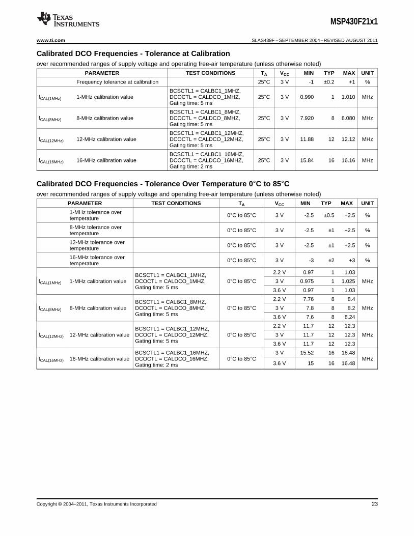
Calibrated DCO Frequencies - Tolerance at Calibrationover recommended ranges of supply voltage and operating free-air temperature (unless otherwise noted)
PARAMETER TEST CONDITIONS TA VCC MIN TYP MAX UNIT
Frequency tolerance at calibration 25°C 3 V -1 ±0.2 +1 %
BCSCTL1 = CALBC1_1MHZ,fCAL(1MHz) 1-MHz calibration value DCOCTL = CALDCO_1MHZ, 25°C 3 V 0.990 1 1.010 MHz
Gating time: 5 ms
BCSCTL1 = CALBC1_8MHZ,fCAL(8MHz) 8-MHz calibration value DCOCTL = CALDCO_8MHZ, 25°C 3 V 7.920 8 8.080 MHz
Gating time: 5 ms
BCSCTL1 = CALBC1_12MHZ,fCAL(12MHz) 12-MHz calibration value DCOCTL = CALDCO_12MHZ, 25°C 3 V 11.88 12 12.12 MHz
Gating time: 5 ms
BCSCTL1 = CALBC1_16MHZ,fCAL(16MHz) 16-MHz calibration value DCOCTL = CALDCO_16MHZ, 25°C 3 V 15.84 16 16.16 MHz
Gating time: 2 ms
Calibrated DCO Frequencies - Tolerance Over Temperature 0°C to 85°Cover recommended ranges of supply voltage and operating free-air temperature (unless otherwise noted)
PARAMETER TEST CONDITIONS TA VCC MIN TYP MAX UNIT
1-MHz tolerance over 0°C to 85°C 3 V -2.5 ±0.5 +2.5 %temperature
8-MHz tolerance over 0°C to 85°C 3 V -2.5 ±1 +2.5 %temperature
12-MHz tolerance over 0°C to 85°C 3 V -2.5 ±1 +2.5 %temperature
16-MHz tolerance over 0°C to 85°C 3 V -3 ±2 +3 %temperature
2.2 V 0.97 1 1.03BCSCTL1 = CALBC1_1MHZ,fCAL(1MHz) 1-MHz calibration value DCOCTL = CALDCO_1MHZ, 0°C to 85°C 3 V 0.975 1 1.025 MHz
Gating time: 5 ms 3.6 V 0.97 1 1.03
2.2 V 7.76 8 8.4BCSCTL1 = CALBC1_8MHZ,fCAL(8MHz) 8-MHz calibration value DCOCTL = CALDCO_8MHZ, 0°C to 85°C 3 V 7.8 8 8.2 MHz
Gating time: 5 ms 3.6 V 7.6 8 8.24
2.2 V 11.7 12 12.3BCSCTL1 = CALBC1_12MHZ,fCAL(12MHz) 12-MHz calibration value DCOCTL = CALDCO_12MHZ, 0°C to 85°C 3 V 11.7 12 12.3 MHz
Gating time: 5 ms 3.6 V 11.7 12 12.3
BCSCTL1 = CALBC1_16MHZ, 3 V 15.52 16 16.48fCAL(16MHz) 16-MHz calibration value DCOCTL = CALDCO_16MHZ, 0°C to 85°C MHz
3.6 V 15 16 16.48Gating time: 2 ms
Copyright © 2004–2011, Texas Instruments Incorporated 23
MSP430F21x1
SLAS439F –SEPTEMBER 2004–REVISED AUGUST 2011 www.ti.com
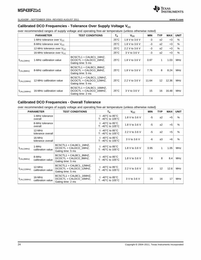
Calibrated DCO Frequencies - Tolerance Over Supply Voltage VCC
over recommended ranges of supply voltage and operating free-air temperature (unless otherwise noted)
PARAMETER TEST CONDITIONS TA VCC MIN TYP MAX UNIT
1-MHz tolerance over VCC 25°C 1.8 V to 3.6 V -3 ±2 +3 %
8-MHz tolerance over VCC 25°C 1.8 V to 3.6 V -3 ±2 +3 %
12-MHz tolerance over VCC 25°C 2.2 V to 3.6 V -3 ±2 +3 %
16-MHz tolerance over VCC 25°C 3 V to 3.6 V -3 ±2 +3 %
BCSCTL1 = CALBC1_1MHZ,fCAL(1MHz) 1-MHz calibration value DCOCTL = CALDCO_1MHZ, 25°C 1.8 V to 3.6 V 0.97 1 1.03 MHz
Gating time: 5 ms
BCSCTL1 = CALBC1_8MHZ,fCAL(8MHz) 8-MHz calibration value DCOCTL = CALDCO_8MHZ, 25°C 1.8 V to 3.6 V 7.76 8 8.24 MHz
Gating time: 5 ms
BCSCTL1 = CALBC1_12MHZ,fCAL(12MHz) 12-MHz calibration value DCOCTL = CALDCO_12MHZ, 25°C 2.2 V to 3.6 V 11.64 12 12.36 MHz
Gating time: 5 ms
BCSCTL1 = CALBC1_16MHZ,fCAL(16MHz) 16-MHz calibration value DCOCTL = CALDCO_16MHZ, 25°C 3 V to 3.6 V 15 16 16.48 MHz
Gating time: 2 ms
Calibrated DCO Frequencies - Overall Toleranceover recommended ranges of supply voltage and operating free-air temperature (unless otherwise noted)
PARAMETER TEST CONDITIONS TA VCC MIN TYP MAX UNIT
1-MHz tolerance I: -40°C to 85°C 1.8 V to 3.6 V -5 ±2 +5 %overall T: -40°C to 105°C8-MHz tolerance I: -40°C to 85°C 1.8 V to 3.6 V -5 ±2 +5 %overall T: -40°C to 105°C12-MHz I: -40°C to 85°C 2.2 V to 3.6 V -5 ±2 +5 %tolerance overall T: -40°C to 105°C16-MHz I: -40°C to 85°C 3 V to 3.6 V -6 ±3 +6 %tolerance overall T: -40°C to 105°C
BCSCTL1 = CALBC1_1MHZ,1-MHz I: -40°C to 85°CfCAL(1MHz) DCOCTL = CALDCO_1MHZ, 1.8 V to 3.6 V 0.95 1 1.05 MHzcalibration value T: -40°C to 105°CGating time: 5 ms
BCSCTL1 = CALBC1_8MHZ,8-MHz I: -40°C to 85°CfCAL(8MHz) DCOCTL = CALDCO_8MHZ, 1.8 V to 3.6 V 7.6 8 8.4 MHzcalibration value T: -40°C to 105°CGating time: 5 ms
BCSCTL1 = CALBC1_12MHZ,12-MHz I: -40°C to 85°CfCAL(12MHz) DCOCTL = CALDCO_12MHZ, 2.2 V to 3.6 V 11.4 12 12.6 MHzcalibration value T: -40°C to 105°CGating time: 5 ms
BCSCTL1 = CALBC1_16MHZ,16-MHz I: -40°C to 85°CfCAL(16MHz) DCOCTL = CALDCO_16MHZ, 3 V to 3.6 V 15 16 17 MHzcalibration value T: -40°C to 105°CGating time: 2 ms
24 Copyright © 2004–2011, Texas Instruments Incorporated
T – Temperature – °CA
0.97
0.98
0.99
1.00
1.01
1.02
1.03
-50
Fre
quency
–M
Hz
V = 1.8 VCC
V = 2.2 VCC
V = 3 VCC
V = 3.6 VCC
-25 0 25 50 75 100
V – Supply Voltage – VCC
0.97
0.98
0.99
1.00
1.01
1.02
1.03
1.5F
requency
–M
Hz T = 105°CA
2.0 2.5 3.0 3.5 4.0
T = 85°CA
T = 25°CA
T = -40°CA
MSP430F21x1
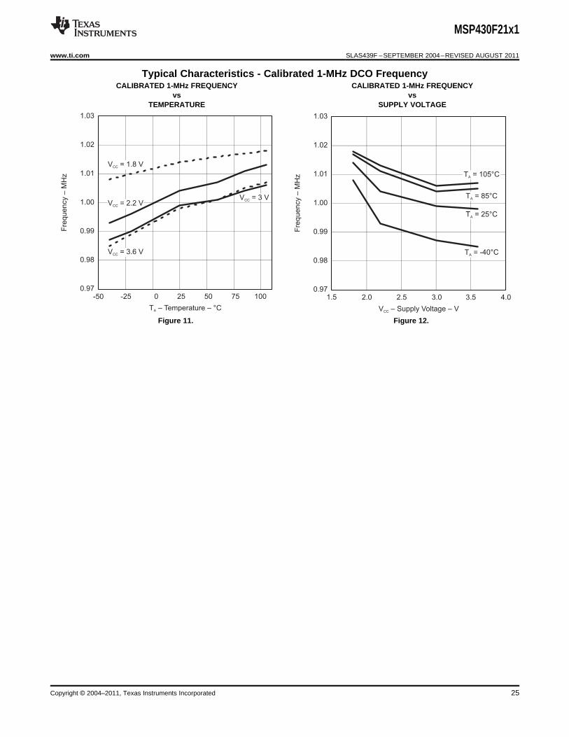
www.ti.com SLAS439F –SEPTEMBER 2004–REVISED AUGUST 2011
Typical Characteristics - Calibrated 1-MHz DCO FrequencyCALIBRATED 1-MHz FREQUENCY CALIBRATED 1-MHz FREQUENCY
vs vsTEMPERATURE SUPPLY VOLTAGE
Figure 11. Figure 12.
Copyright © 2004–2011, Texas Instruments Incorporated 25
DCO Frequency − MHz
0.10
1.00
10.00
0.10 1.00 10.00
DC
O W
ake
Tim
e−
µs
RSELx = 0 to 11RSELx = 12 to 15
MSP430F21x1
SLAS439F –SEPTEMBER 2004–REVISED AUGUST 2011 www.ti.com
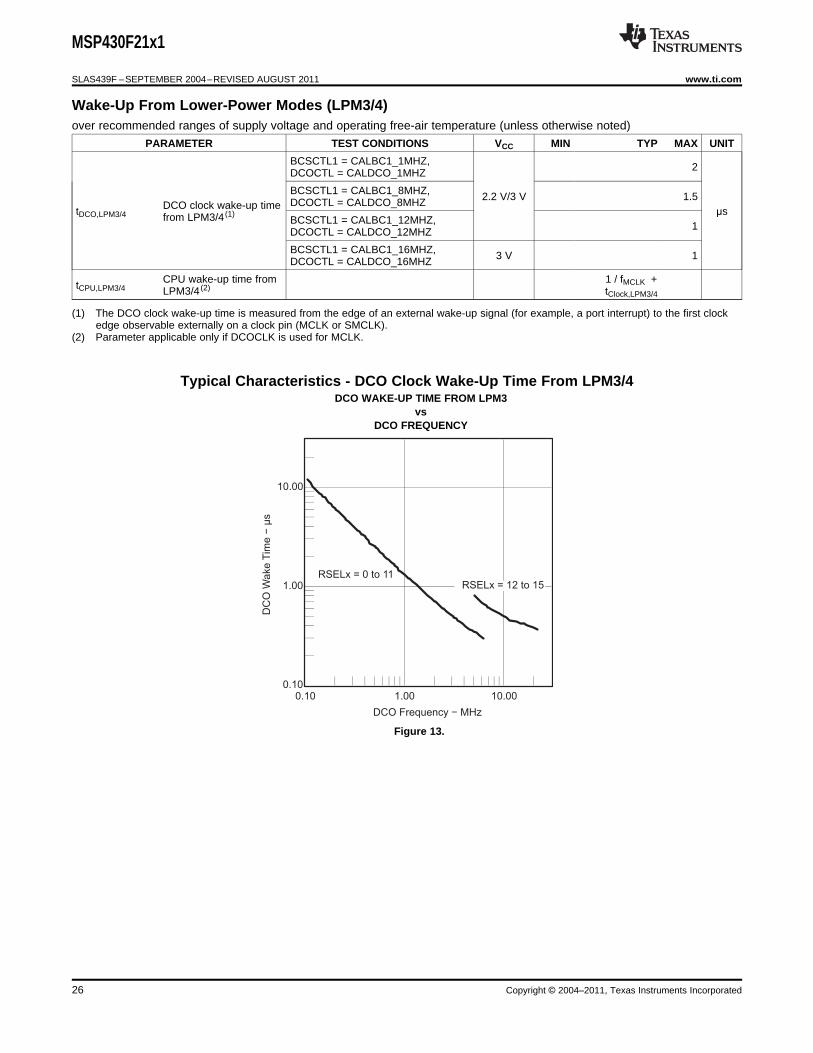
Wake-Up From Lower-Power Modes (LPM3/4)over recommended ranges of supply voltage and operating free-air temperature (unless otherwise noted)
PARAMETER TEST CONDITIONS VCC MIN TYP MAX UNIT
BCSCTL1 = CALBC1_1MHZ, 2DCOCTL = CALDCO_1MHZ
BCSCTL1 = CALBC1_8MHZ, 2.2 V/3 V 1.5DCOCTL = CALDCO_8MHZDCO clock wake-up timetDCO,LPM3/4 µsfrom LPM3/4 (1)BCSCTL1 = CALBC1_12MHZ, 1DCOCTL = CALDCO_12MHZ
BCSCTL1 = CALBC1_16MHZ, 3 V 1DCOCTL = CALDCO_16MHZ
CPU wake-up time from 1 / fMCLK +tCPU,LPM3/4 LPM3/4 (2) tClock,LPM3/4
(1) The DCO clock wake-up time is measured from the edge of an external wake-up signal (for example, a port interrupt) to the first clockedge observable externally on a clock pin (MCLK or SMCLK).
(2) Parameter applicable only if DCOCLK is used for MCLK.
Typical Characteristics - DCO Clock Wake-Up Time From LPM3/4DCO WAKE-UP TIME FROM LPM3
vsDCO FREQUENCY
Figure 13.
26 Copyright © 2004–2011, Texas Instruments Incorporated
MSP430F21x1
www.ti.com SLAS439F –SEPTEMBER 2004–REVISED AUGUST 2011
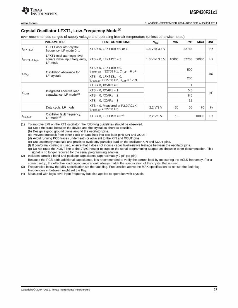
Crystal Oscillator LFXT1, Low-Frequency Mode (1)
over recommended ranges of supply voltage and operating free-air temperature (unless otherwise noted)
PARAMETER TEST CONDITIONS VCC MIN TYP MAX UNIT
LFXT1 oscillator crystalfLFXT1,LF XTS = 0, LFXT1Sx = 0 or 1 1.8 V to 3.6 V 32768 Hzfrequency, LF mode 0, 1
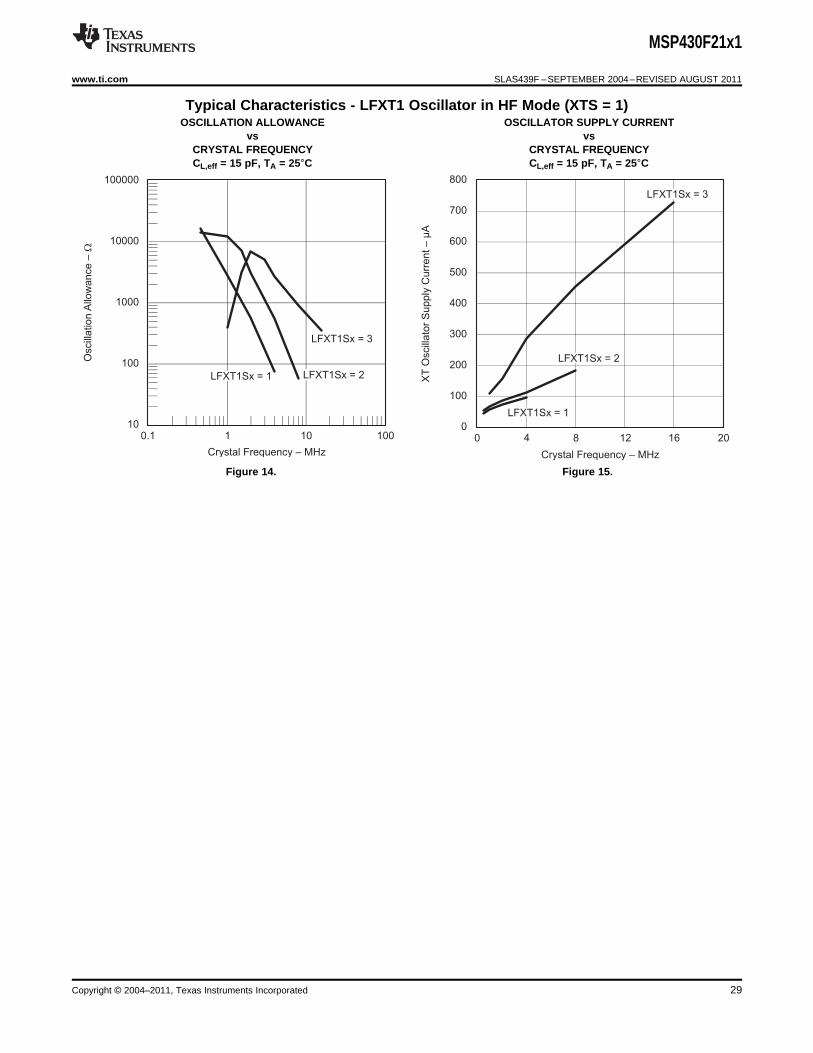
LFXT1 oscillator logic levelfLFXT1,LF,logic square wave input frequency, XTS = 0, LFXT1Sx = 3 1.8 V to 3.6 V 10000 32768 50000 Hz
LF mode
XTS = 0, LFXT1Sx = 0, 500fLFXT1,LF = 32768 Hz, CL,eff = 6 pFOscillation allowance forOALF kΩLF crystals XTS = 0, LFXT1Sx = 0, 200fLFXT1,LF = 32768 Hz, CL,eff = 12 pF
XTS = 0, XCAPx = 0 1
XTS = 0, XCAPx = 1 5.5Integrated effective loadCL,eff pFcapacitance, LF mode (2)XTS = 0, XCAPx = 2 8.5
XTS = 0, XCAPx = 3 11
XTS = 0, Measured at P2.0/ACLK,Duty cycle, LF mode 2.2 V/3 V 30 50 70 %fLFXT1,LF = 32768 Hz
Oscillator fault frequency,fFault,LF XTS = 0, LFXT1Sx = 3 (4) 2.2 V/3 V 10 10000 HzLF mode (3)
(1) To improve EMI on the XT1 oscillator, the following guidelines should be observed.(a) Keep the trace between the device and the crystal as short as possible.(b) Design a good ground plane around the oscillator pins.(c) Prevent crosstalk from other clock or data lines into oscillator pins XIN and XOUT.(d) Avoid running PCB traces underneath or adjacent to the XIN and XOUT pins.(e) Use assembly materials and praxis to avoid any parasitic load on the oscillator XIN and XOUT pins.(f) If conformal coating is used, ensure that it does not induce capacitive/resistive leakage between the oscillator pins.(g) Do not route the XOUT line to the JTAG header to support the serial programming adapter as shown in other documentation. This
signal is no longer required for the serial programming adapter.(2) Includes parasitic bond and package capacitance (approximately 2 pF per pin).
Because the PCB adds additional capacitance, it is recommended to verify the correct load by measuring the ACLK frequency. For acorrect setup, the effective load capacitance should always match the specification of the crystal that is used.
(3) Frequencies below the MIN specification set the fault flag. Frequencies above the MAX specification do not set the fault flag.Frequencies in between might set the flag.
(4) Measured with logic-level input frequency but also applies to operation with crystals.
Copyright © 2004–2011, Texas Instruments Incorporated 27
MSP430F21x1
SLAS439F –SEPTEMBER 2004–REVISED AUGUST 2011 www.ti.com
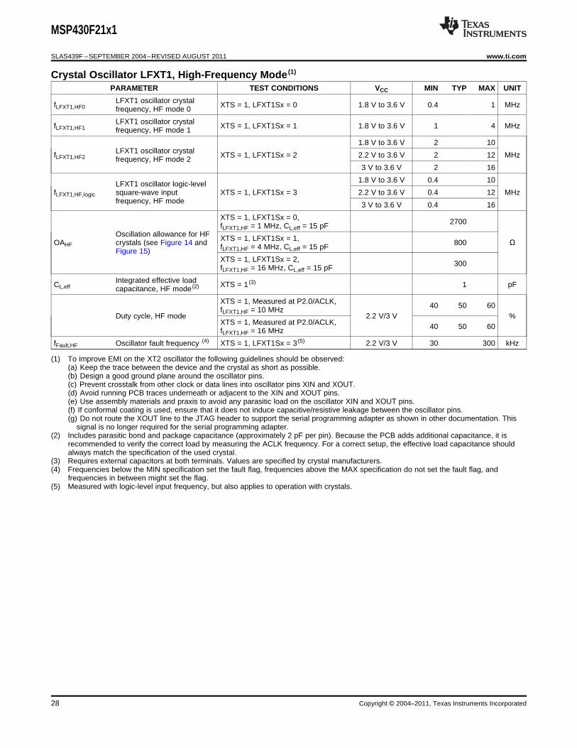
Crystal Oscillator LFXT1, High-Frequency Mode (1)
PARAMETER TEST CONDITIONS VCC MIN TYP MAX UNIT
LFXT1 oscillator crystalfLFXT1,HF0 XTS = 1, LFXT1Sx = 0 1.8 V to 3.6 V 0.4 1 MHzfrequency, HF mode 0
LFXT1 oscillator crystalfLFXT1,HF1 XTS = 1, LFXT1Sx = 1 1.8 V to 3.6 V 1 4 MHzfrequency, HF mode 1
1.8 V to 3.6 V 2 10LFXT1 oscillator crystalfLFXT1,HF2 XTS = 1, LFXT1Sx = 2 2.2 V to 3.6 V 2 12 MHzfrequency, HF mode 2
3 V to 3.6 V 2 16
1.8 V to 3.6 V 0.4 10LFXT1 oscillator logic-levelfLFXT1,HF,logic square-wave input XTS = 1, LFXT1Sx = 3 2.2 V to 3.6 V 0.4 12 MHz
frequency, HF mode 3 V to 3.6 V 0.4 16
XTS = 1, LFXT1Sx = 0, 2700fLFXT1,HF = 1 MHz, CL,eff = 15 pFOscillation allowance for HF XTS = 1, LFXT1Sx = 1,OAHF crystals (see Figure 14 and 800 ΩfLFXT1,HF = 4 MHz, CL,eff = 15 pFFigure 15)
XTS = 1, LFXT1Sx = 2, 300fLFXT1,HF = 16 MHz, CL,eff = 15 pF
Integrated effective loadCL,eff XTS = 1 (3) 1 pFcapacitance, HF mode (2)
XTS = 1, Measured at P2.0/ACLK, 40 50 60fLFXT1,HF = 10 MHzDuty cycle, HF mode 2.2 V/3 V %
XTS = 1, Measured at P2.0/ACLK, 40 50 60fLFXT1,HF = 16 MHz
fFault,HF Oscillator fault frequency (4) XTS = 1, LFXT1Sx = 3 (5) 2.2 V/3 V 30 300 kHz
(1) To improve EMI on the XT2 oscillator the following guidelines should be observed:(a) Keep the trace between the device and the crystal as short as possible.(b) Design a good ground plane around the oscillator pins.(c) Prevent crosstalk from other clock or data lines into oscillator pins XIN and XOUT.(d) Avoid running PCB traces underneath or adjacent to the XIN and XOUT pins.(e) Use assembly materials and praxis to avoid any parasitic load on the oscillator XIN and XOUT pins.(f) If conformal coating is used, ensure that it does not induce capacitive/resistive leakage between the oscillator pins.(g) Do not route the XOUT line to the JTAG header to support the serial programming adapter as shown in other documentation. This
signal is no longer required for the serial programming adapter.(2) Includes parasitic bond and package capacitance (approximately 2 pF per pin). Because the PCB adds additional capacitance, it is
recommended to verify the correct load by measuring the ACLK frequency. For a correct setup, the effective load capacitance shouldalways match the specification of the used crystal.
(3) Requires external capacitors at both terminals. Values are specified by crystal manufacturers.(4) Frequencies below the MIN specification set the fault flag, frequencies above the MAX specification do not set the fault flag, and
frequencies in between might set the flag.(5) Measured with logic-level input frequency, but also applies to operation with crystals.
28 Copyright © 2004–2011, Texas Instruments Incorporated
Crystal Frequency – MHz
10
100
1000
10000
100000
0.1
Oscill
ation
Allo
wance
–W
LFXT1Sx = 1
LFXT1Sx = 3
1 10 100
LFXT1Sx = 2
0
100
200
300
400
500
600
700
800
0
Crystal Frequency – MHz
XT
Oscill
ato
r S
upply
Curr
ent–
µA
LFXT1Sx = 1
LFXT1Sx = 2
LFXT1Sx = 3
4 8 12 16 20
MSP430F21x1
www.ti.com SLAS439F –SEPTEMBER 2004–REVISED AUGUST 2011
Typical Characteristics - LFXT1 Oscillator in HF Mode (XTS = 1)OSCILLATION ALLOWANCE OSCILLATOR SUPPLY CURRENT
vs vsCRYSTAL FREQUENCY CRYSTAL FREQUENCYCL,eff = 15 pF, TA = 25°C CL,eff = 15 pF, TA = 25°C
Figure 14. Figure 15.
Copyright © 2004–2011, Texas Instruments Incorporated 29
MSP430F21x1
SLAS439F –SEPTEMBER 2004–REVISED AUGUST 2011 www.ti.com
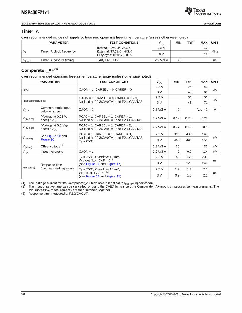
Timer_Aover recommended ranges of supply voltage and operating free-air temperature (unless otherwise noted)
PARAMETER TEST CONDITIONS VCC MIN TYP MAX UNIT
Internal: SMCLK, ACLK 2.2 V 10fTA Timer_A clock frequency External: TACLK, INCLK MHz
3 V 16Duty cycle = 50% ± 10%
tTA,cap Timer_A capture timing TA0, TA1, TA2 2.2 V/3 V 20 ns
Comparator_A+ (1)
over recommended operating free-air temperature range (unless otherwise noted)
PARAMETER TEST CONDITIONS VCC MIN TYP MAX UNIT
2.2 V 25 40I(DD) CAON = 1, CARSEL = 0, CAREF = 0 µA
3 V 45 60
2.2 V 30 50CAON = 1, CARSEL = 0, CAREF = 1/2/3,I(Refladder/RefDiode) µANo load at P2.3/CA0/TA1 and P2.4/CA1/TA2 3 V 45 71
Common-mode inputV(IC) CAON = 1 2.2 V/3 V 0 VCC - 1 Vvoltage range
(Voltage at 0.25 VCC PCA0 = 1, CARSEL = 1, CAREF = 1,V(Ref025) 2.2 V/3 V 0.23 0.24 0.25node) / VCC No load at P2.3/CA0/TA1 and P2.4/CA1/TA2
(Voltage at 0.5 VCC PCA0 = 1, CARSEL = 1, CAREF = 2,V(Ref050) 2.2 V/3 V 0.47 0.48 0.5node) / VCC No load at P2.3/CA0/TA1 and P2.4/CA1/TA2
PCA0 = 1, CARSEL = 1, CAREF = 3, 2.2 V 390 480 540See Figure 19 andV(RefVT) No load at P2.3/CA0/TA1 and P2.4/CA1/TA2, mVFigure 20 3 V 400 490 550TA = 85°CV(offset) Offset voltage (2) 2.2 V/3 V -30 30 mV
Vhys Input hysteresis CAON = 1 2.2 V/3 V 0 0.7 1.4 mV
TA = 25°C, Overdrive 10 mV, 2.2 V 80 165 300Without filter: CAF = 0 (3) ns
3 V 70 120 240(see Figure 16 and Figure 17)Response timet(response) (low-high and high-low) TA = 25°C, Overdrive 10 mV, 2.2 V 1.4 1.9 2.8With filter: CAF = 1 (3) µs
3 V 0.9 1.5 2.2(see Figure 16 and Figure 17)
(1) The leakage current for the Comparator_A+ terminals is identical to Ilkg(Px.y) specification.(2) The input offset voltage can be cancelled by using the CAEX bit to invert the Comparator_A+ inputs on successive measurements. The
two successive measurements are then summed together.(3) Response time measured at P2.2/CAOUT.
30 Copyright © 2004–2011, Texas Instruments Incorporated
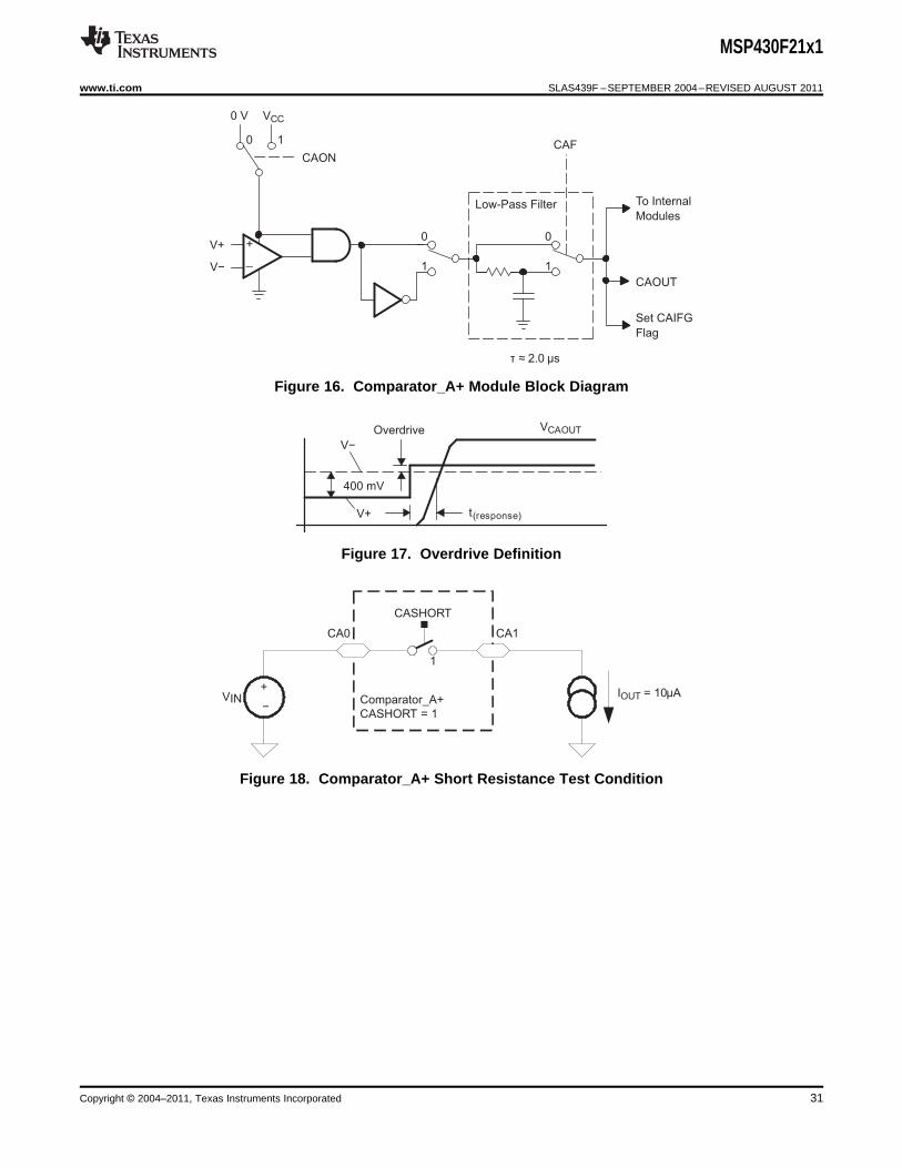
_
+
CAON
0
1
V+0
1
CAF
Low-Pass Filter
τ ≈ 2.0 µs
To Internal
Modules
Set CAIFG
Flag
CAOUT
V−
VCC
1
0 V
0
Overdrive VCAOUT
t(response)V+
V−
400 mV
CASHORT
1
Comparator_A+
CASHORT = 1
CA1CA0
VIN+
−
IOUT = 10µA
MSP430F21x1
www.ti.com SLAS439F –SEPTEMBER 2004–REVISED AUGUST 2011
Figure 16. Comparator_A+ Module Block Diagram
Figure 17. Overdrive Definition
Figure 18. Comparator_A+ Short Resistance Test Condition
Copyright © 2004–2011, Texas Instruments Incorporated 31
T – Free-Air Temperature – °CA
400
450
500
550
600
650
V–
Re
fere
nce
Vo
lts
–m
V(R
EF
VT
)
-45 -25 -5 15 35 55 75 95
V = 3 VCC
Typical
V = 2.2 VCC
Typical
T – Free-Air Temperature – °CA
400
450
500
550
600
650
V–
Re
fere
nce
Vo
lts
–m
V(R
EF
VT
)
-45 -25 -5 15 35 55 75 95
V /V – Normalized Input Voltage – V/VIN CC
1
10
100
0
Short
Resis
tance
–kW
V = 1.8 VCC
V = 3.6 VCC
V = 2.2 VCC
V = 3 VCC
0.2 0.4 0.6 0.8 1.0
MSP430F21x1
SLAS439F –SEPTEMBER 2004–REVISED AUGUST 2011 www.ti.com
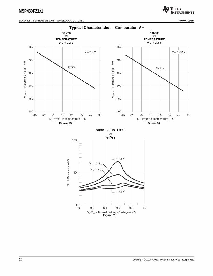
Typical Characteristics - Comparator_A+V(RefVT) V(RefVT)
vs vsTEMPERATURE TEMPERATURE
VCC = 2.2 V VCC = 2.2 V
Figure 19. Figure 20.
SHORT RESISTANCEvs
VIN/VCC
Figure 21.
32 Copyright © 2004–2011, Texas Instruments Incorporated
MSP430F21x1
www.ti.com SLAS439F –SEPTEMBER 2004–REVISED AUGUST 2011
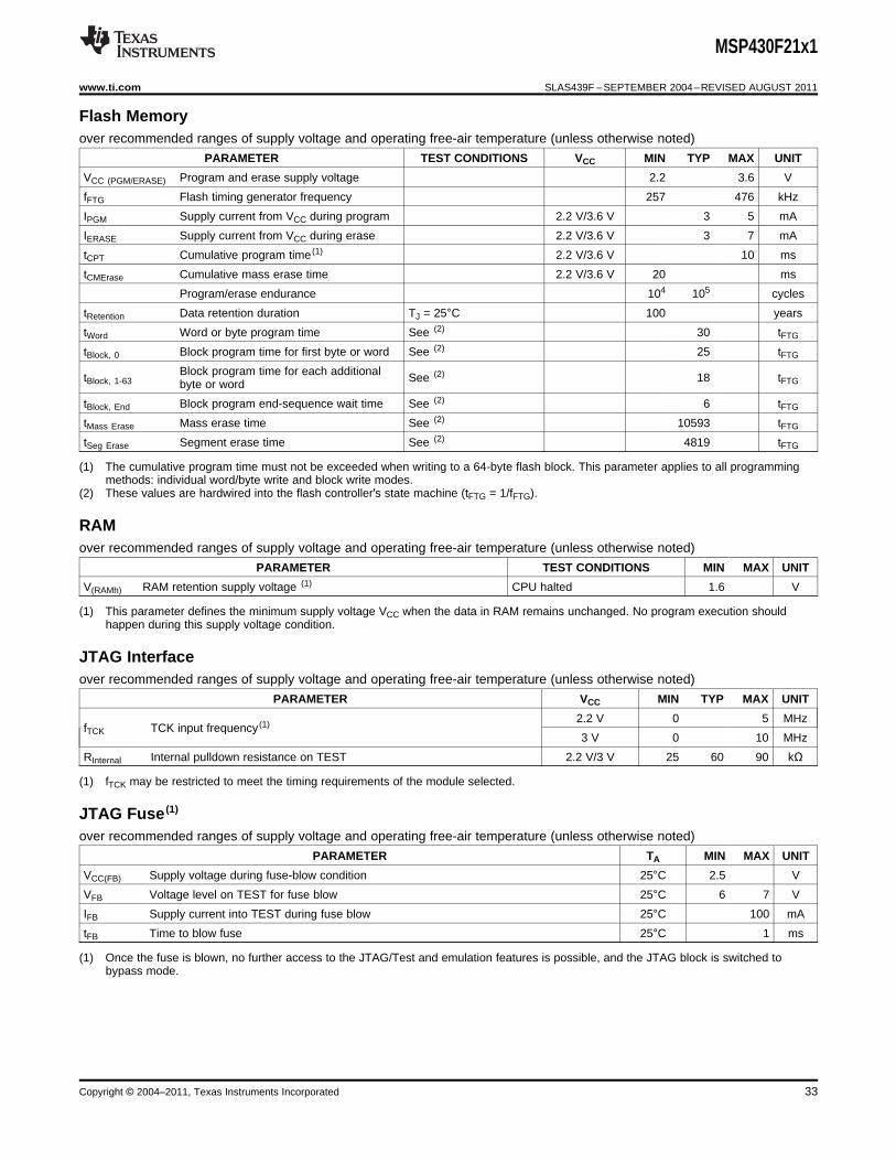
Flash Memoryover recommended ranges of supply voltage and operating free-air temperature (unless otherwise noted)
PARAMETER TEST CONDITIONS VCC MIN TYP MAX UNIT
VCC (PGM/ERASE) Program and erase supply voltage 2.2 3.6 V
fFTG Flash timing generator frequency 257 476 kHz
IPGM Supply current from VCC during program 2.2 V/3.6 V 3 5 mA
IERASE Supply current from VCC during erase 2.2 V/3.6 V 3 7 mA
tCPT Cumulative program time (1) 2.2 V/3.6 V 10 ms
tCMErase Cumulative mass erase time 2.2 V/3.6 V 20 ms
Program/erase endurance 104 105 cycles
tRetention Data retention duration TJ = 25°C 100 years
tWord Word or byte program time See (2) 30 tFTG
tBlock, 0 Block program time for first byte or word See (2) 25 tFTG
Block program time for each additionaltBlock, 1-63 See (2) 18 tFTGbyte or word
tBlock, End Block program end-sequence wait time See (2) 6 tFTG
tMass Erase Mass erase time See (2) 10593 tFTG
tSeg Erase Segment erase time See (2) 4819 tFTG
(1) The cumulative program time must not be exceeded when writing to a 64-byte flash block. This parameter applies to all programmingmethods: individual word/byte write and block write modes.
(2) These values are hardwired into the flash controller's state machine (tFTG = 1/fFTG).
RAMover recommended ranges of supply voltage and operating free-air temperature (unless otherwise noted)
PARAMETER TEST CONDITIONS MIN MAX UNIT
V(RAMh) RAM retention supply voltage (1) CPU halted 1.6 V
(1) This parameter defines the minimum supply voltage VCC when the data in RAM remains unchanged. No program execution shouldhappen during this supply voltage condition.
JTAG Interfaceover recommended ranges of supply voltage and operating free-air temperature (unless otherwise noted)
PARAMETER VCC MIN TYP MAX UNIT
2.2 V 0 5 MHzfTCK TCK input frequency (1)
3 V 0 10 MHz
RInternal Internal pulldown resistance on TEST 2.2 V/3 V 25 60 90 kΩ
(1) fTCK may be restricted to meet the timing requirements of the module selected.
JTAG Fuse (1)
over recommended ranges of supply voltage and operating free-air temperature (unless otherwise noted)
PARAMETER TA MIN MAX UNIT
VCC(FB) Supply voltage during fuse-blow condition 25°C 2.5 V
VFB Voltage level on TEST for fuse blow 25°C 6 7 V
IFB Supply current into TEST during fuse blow 25°C 100 mA
tFB Time to blow fuse 25°C 1 ms
(1) Once the fuse is blown, no further access to the JTAG/Test and emulation features is possible, and the JTAG block is switched tobypass mode.
Copyright © 2004–2011, Texas Instruments Incorporated 33
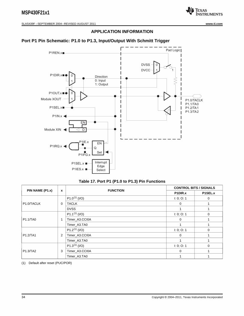
Direction
0: Input
1: Output
P1SEL.x
1
0P1DIR.x
P1IN.x
P1IRQ.x
D
EN
Module XIN
1
0
Module XOUT
P1OUT.x
Interrupt
Edge
Select
Q
EN
Set
P1SEL.x
P1IES.x
P1IFG.x
P1IE.x
P1.0/TACLK
P1.1/TA0
P1.2/TA1
P1.3/TA2
1
0DVSS
DVCC
P1REN.xPad Logic
1
MSP430F21x1
SLAS439F –SEPTEMBER 2004–REVISED AUGUST 2011 www.ti.com
APPLICATION INFORMATION
Port P1 Pin Schematic: P1.0 to P1.3, Input/Output With Schmitt Trigger
Table 17. Port P1 (P1.0 to P1.3) Pin Functions
CONTROL BITS / SIGNALSPIN NAME (P1.x) x FUNCTION
P1DIR.x P1SEL.x
P1.0 (1) (I/O) I: 0; O: 1 0
P1.0/TACLK 0 TACLK 0 1
DVSS 1 1
P1.1 (1) (I/O) I: 0; O: 1 0
P1.1/TA0 1 Timer_A3.CCI0A 0 1
Timer_A3.TA0 1 1
P1.2 (1) (I/O) I: 0; O: 1 0
P1.2/TA1 2 Timer_A3.CCI0A 0 1
Timer_A3.TA0 1 1
P1.3 (1) (I/O) I: 0; O: 1 0
P1.3/TA2 3 Timer_A3.CCI0A 0 1
Timer_A3.TA0 1 1
(1) Default after reset (PUC/POR)
34 Copyright © 2004–2011, Texas Instruments Incorporated
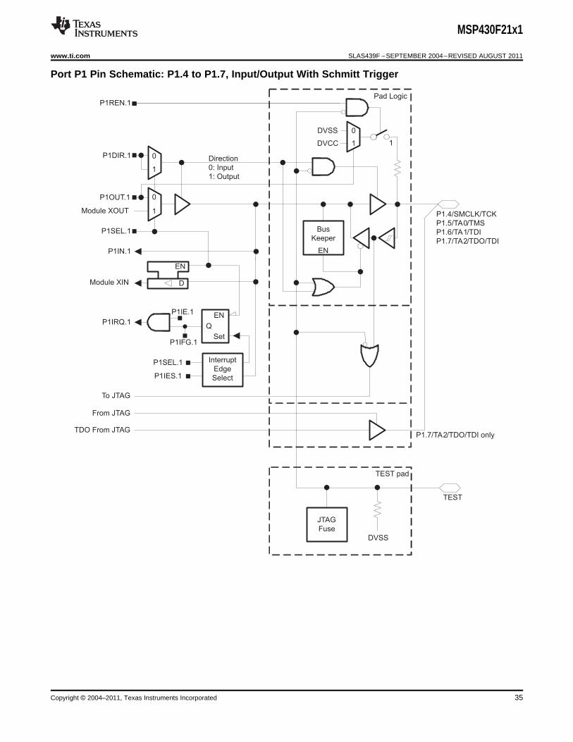
Bus
Keeper
EN
Direction
0: Input
1: Output
P1SEL.1
1
0P1DIR.1
P1IN.1
P1IRQ.1
D
EN
Module XIN
1
0
Module XOUT
P1OUT.1
Interrupt
Edge
Select
Q
EN
Set
P1SEL.1
P1IES.1
P1IFG.1
P1IE.1
1
0DVSS
DVCC
P1REN.1Pad Logic
1
TEST pad
TEST
JTAG
Fuse
DVSS
From JTAG
TDO From JTAGP1.7/TA2/TDO/TDI only
P1.4/SMCLK/TCK
P1.5/TA0/TMS
P1.6/TA1/TDI
P1.7/TA2/TDO/TDI
To JTAG
MSP430F21x1
www.ti.com SLAS439F –SEPTEMBER 2004–REVISED AUGUST 2011
Port P1 Pin Schematic: P1.4 to P1.7, Input/Output With Schmitt Trigger
Copyright © 2004–2011, Texas Instruments Incorporated 35
MSP430F21x1
SLAS439F –SEPTEMBER 2004–REVISED AUGUST 2011 www.ti.com
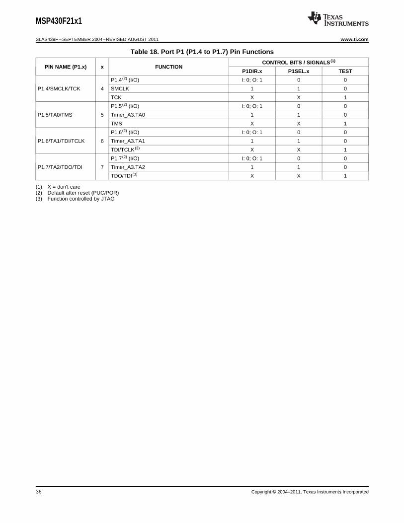
Table 18. Port P1 (P1.4 to P1.7) Pin Functions
CONTROL BITS / SIGNALS (1)
PIN NAME (P1.x) x FUNCTIONP1DIR.x P1SEL.x TEST
P1.4 (2) (I/O) I: 0; O: 1 0 0
P1.4/SMCLK/TCK 4 SMCLK 1 1 0
TCK X X 1
P1.5 (2) (I/O) I: 0; O: 1 0 0
P1.5/TA0/TMS 5 Timer_A3.TA0 1 1 0
TMS X X 1
P1.6 (2) (I/O) I: 0; O: 1 0 0
P1.6/TA1/TDI/TCLK 6 Timer_A3.TA1 1 1 0
TDI/TCLK (3) X X 1
P1.7 (2) (I/O) I: 0; O: 1 0 0
P1.7/TA2/TDO/TDI 7 Timer_A3.TA2 1 1 0
TDO/TDI (3) X X 1
(1) X = don't care(2) Default after reset (PUC/POR)(3) Function controlled by JTAG
36 Copyright © 2004–2011, Texas Instruments Incorporated

Bus
Keeper
EN
Direction
0: Input
1: Output
P2SEL.x
1
0P2DIR.x
P2IN.x
P2IRQ.x
D
EN
Module XIN
1
0
Module XOUT
P2OUT.x
Interrupt
Edge
Select
Q
EN
Set
P2SEL.x
P2IES.x
P2IFG.x
P2IE.x
1
0DVSS
DVCC
P2REN.x
CAPD.x
Pad Logic
From Comparator_A+
To Comparator_A+
1
P2.0/ACLK/CA2
P2.1/INCLK/CA3
P2.2/CAOUT/TA0/CA4
P2.3/TA1/CA0
P2.4/TA2/CA1
P2.5/CA5
MSP430F21x1
www.ti.com SLAS439F –SEPTEMBER 2004–REVISED AUGUST 2011
Port P2 Pin Schematic: P2.0 to P2.5, Input/Output With Schmitt Trigger
Table 19. Control Signal "From Comparator_A+"SIGNAL "From Comparator_A+" = 1 (1)
PIN NAME FUNCTIONP2CA4 P2CA0 P2CA3 P2CA2 P2CA1
P2.0/ACLK/CA2 CA2 1 1 0 1 0
P2.1/INCLK/CA3 CA3 N/A N/A 0 1 1
P2.2/CAOUT/TA0/CA4 CA4 N/A N/A 1 0 0OR
P2.3/TA1/CA0 CA0 0 1 N/A N/A N/A
P2.4/TA2/CA1 CA1 1 0 0 0 1
P2.5/CA5 CA5 N/A N/A 1 0 1
(1) N/A = Not available or not applicable
Copyright © 2004–2011, Texas Instruments Incorporated 37
MSP430F21x1
SLAS439F –SEPTEMBER 2004–REVISED AUGUST 2011 www.ti.com
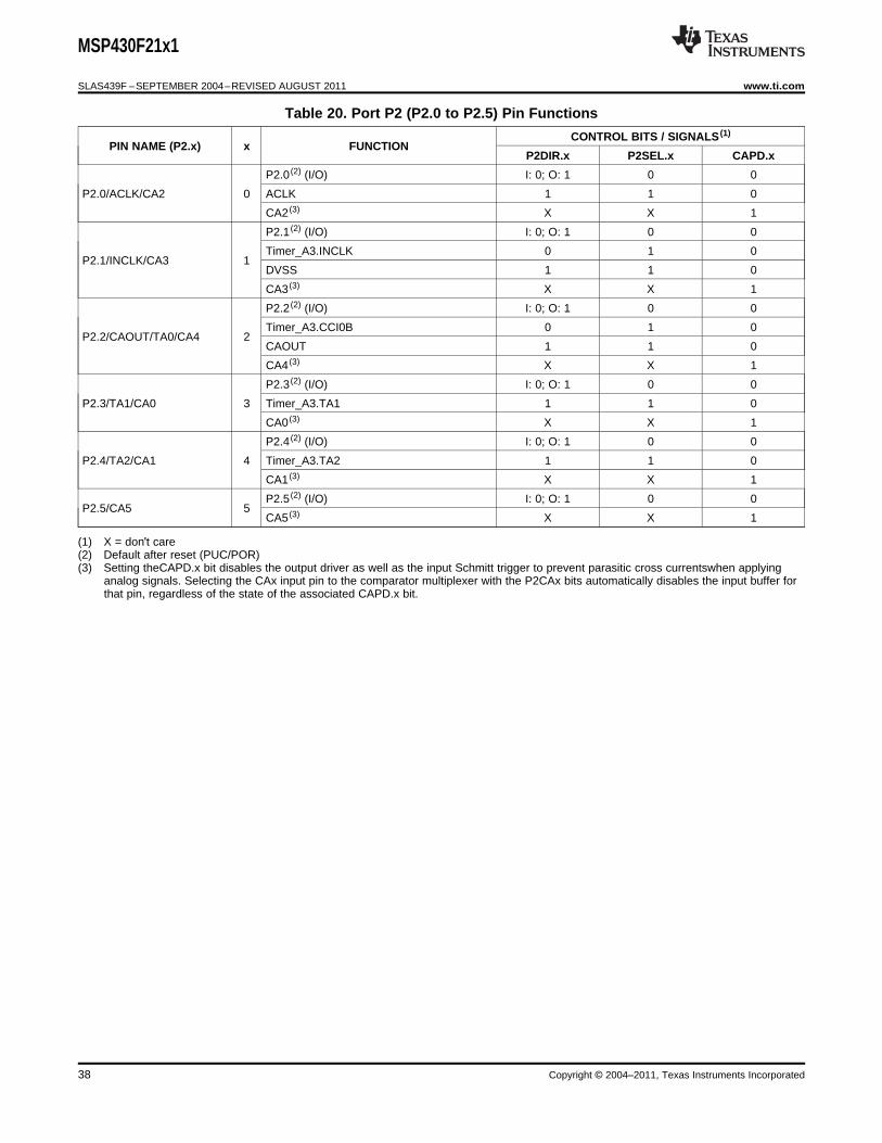
Table 20. Port P2 (P2.0 to P2.5) Pin Functions
CONTROL BITS / SIGNALS (1)
PIN NAME (P2.x) x FUNCTIONP2DIR.x P2SEL.x CAPD.x
P2.0 (2) (I/O) I: 0; O: 1 0 0
P2.0/ACLK/CA2 0 ACLK 1 1 0
CA2 (3) X X 1
P2.1 (2) (I/O) I: 0; O: 1 0 0
Timer_A3.INCLK 0 1 0P2.1/INCLK/CA3 1
DVSS 1 1 0
CA3 (3) X X 1
P2.2 (2) (I/O) I: 0; O: 1 0 0
Timer_A3.CCI0B 0 1 0P2.2/CAOUT/TA0/CA4 2
CAOUT 1 1 0
CA4 (3) X X 1
P2.3 (2) (I/O) I: 0; O: 1 0 0
P2.3/TA1/CA0 3 Timer_A3.TA1 1 1 0
CA0 (3) X X 1
P2.4 (2) (I/O) I: 0; O: 1 0 0
P2.4/TA2/CA1 4 Timer_A3.TA2 1 1 0
CA1 (3) X X 1
P2.5 (2) (I/O) I: 0; O: 1 0 0P2.5/CA5 5
CA5 (3) X X 1
(1) X = don't care(2) Default after reset (PUC/POR)(3) Setting theCAPD.x bit disables the output driver as well as the input Schmitt trigger to prevent parasitic cross currentswhen applying
analog signals. Selecting the CAx input pin to the comparator multiplexer with the P2CAx bits automatically disables the input buffer forthat pin, regardless of the state of the associated CAPD.x bit.
38 Copyright © 2004–2011, Texas Instruments Incorporated

Bus
Keeper
EN
Direction
0: Input
1: Output
P2SEL.6
1
0P2DIR.6
P2IN.6
P2IRQ.6
D
EN
Module XIN
1
0
Module XOUT
P2OUT.6
Interrupt
Edge
Select
Q
EN
Set
P2SEL.6
P2IES.6
P2IFG.6
P2IE.6
P2.6/XIN/CA6
1
0DVSS
DVCC
P2REN.6
LFXT1 OscillatorBCSCTL3.LFXT1Sx = 11
P2.7/XOUT/CA7
LFXT1 off
0
1
1
LFXT1CLK
CAPD.x
Pad Logic
From Comparator_A+
To Comparator_A+
P2SEL.7
MSP430F21x1
www.ti.com SLAS439F –SEPTEMBER 2004–REVISED AUGUST 2011
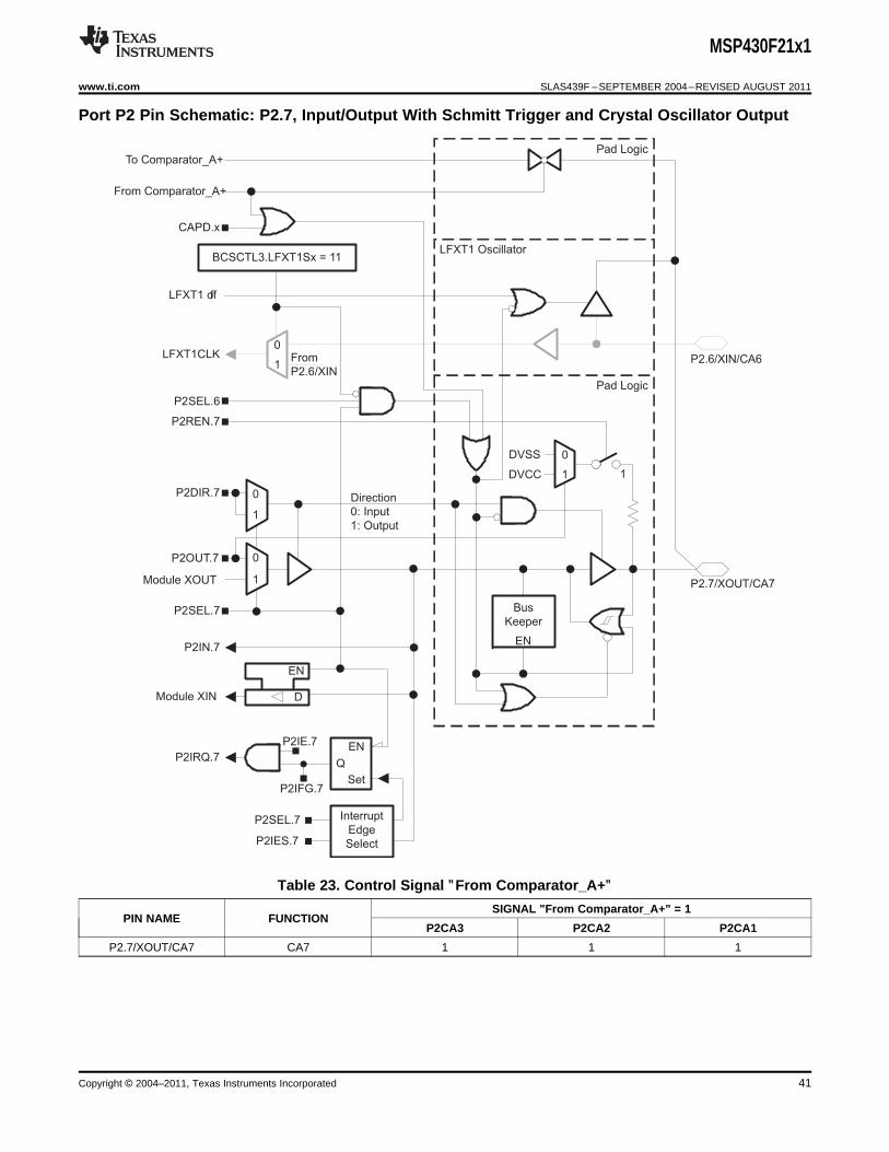
Port P2 Pin Schematic: P2.6, Input/Output With Schmitt Trigger and Crystal Oscillator Input
Table 21. Control Signal "From Comparator_A+"SIGNAL "From Comparator_A+" = 1
PIN NAME FUNCTIONP2CA3 P2CA2 P2CA1
P2.6/XIN/CA6 CA6 1 1 0
Copyright © 2004–2011, Texas Instruments Incorporated 39
MSP430F21x1
SLAS439F –SEPTEMBER 2004–REVISED AUGUST 2011 www.ti.com
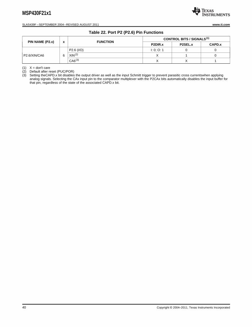
Table 22. Port P2 (P2.6) Pin Functions
CONTROL BITS / SIGNALS (1)
PIN NAME (P2.x) x FUNCTIONP2DIR.x P2SEL.x CAPD.x
P2.6 (I/O) I: 0; O: 1 0 0
P2.6/XIN/CA6 6 XIN (2) X 1 0
CA6 (3) X X 1
(1) X = don't care(2) Default after reset (PUC/POR)(3) Setting theCAPD.x bit disables the output driver as well as the input Schmitt trigger to prevent parasitic cross currentswhen applying
analog signals. Selecting the CAx input pin to the comparator multiplexer with the P2CAx bits automatically disables the input buffer forthat pin, regardless of the state of the associated CAPD.x bit.
40 Copyright © 2004–2011, Texas Instruments Incorporated
Bus
Keeper
EN
Direction
0: Input
1: Output
P2SEL.7
1
0P2DIR.7
P2IN.7
P2IRQ.7
D
EN
Module XIN
1
0
Module XOUT
P2OUT.7
Interrupt
Edge
Select
Q
EN
Set
P2SEL.7
P2IES.7
P2IFG.7
P2IE.7
P2.7/XOUT/CA7
1
0DVSS
DVCC
P2REN.7
Pad Logic
LFXT1 OscillatorBCSCTL3.LFXT1Sx = 11
LFXT1 off
0
1
1
LFXT1CLK P2.6/XIN/CA6
CAPD.x
Pad Logic
From Comparator_A+
To Comparator_A+
P2SEL.6
From
P2.6/XIN
MSP430F21x1
www.ti.com SLAS439F –SEPTEMBER 2004–REVISED AUGUST 2011
Port P2 Pin Schematic: P2.7, Input/Output With Schmitt Trigger and Crystal Oscillator Output
Table 23. Control Signal "From Comparator_A+"SIGNAL "From Comparator_A+" = 1
PIN NAME FUNCTIONP2CA3 P2CA2 P2CA1
P2.7/XOUT/CA7 CA7 1 1 1
Copyright © 2004–2011, Texas Instruments Incorporated 41
MSP430F21x1
SLAS439F –SEPTEMBER 2004–REVISED AUGUST 2011 www.ti.com
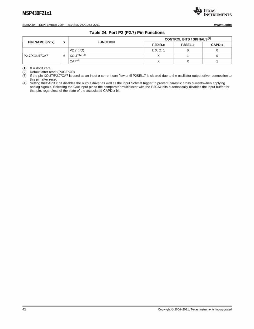
Table 24. Port P2 (P2.7) Pin Functions
CONTROL BITS / SIGNALS (1)
PIN NAME (P2.x) x FUNCTIONP2DIR.x P2SEL.x CAPD.x
P2.7 (I/O) I: 0; O: 1 0 0
P2.7/XOUT/CA7 6 XOUT (2) (3) X 1 0
CA7 (4) X X 1
(1) X = don't care(2) Default after reset (PUC/POR)(3) If the pin XOUT/P2.7/CA7 is used as an input a current can flow until P2SEL.7 is cleared due to the oscillator output driver connection to
this pin after reset.(4) Setting theCAPD.x bit disables the output driver as well as the input Schmitt trigger to prevent parasitic cross currentswhen applying
analog signals. Selecting the CAx input pin to the comparator multiplexer with the P2CAx bits automatically disables the input buffer forthat pin, regardless of the state of the associated CAPD.x bit.
42 Copyright © 2004–2011, Texas Instruments Incorporated
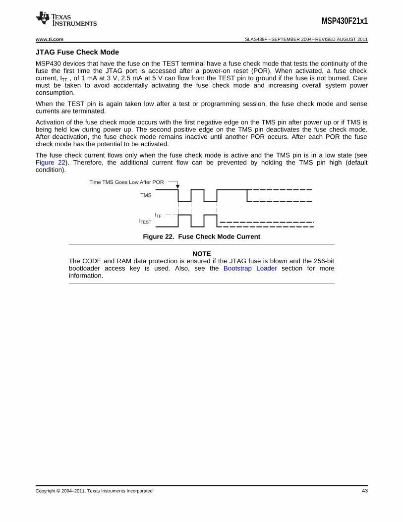
Time TMS Goes Low After POR
TMS
ITF
ITEST
MSP430F21x1
www.ti.com SLAS439F –SEPTEMBER 2004–REVISED AUGUST 2011
JTAG Fuse Check Mode
MSP430 devices that have the fuse on the TEST terminal have a fuse check mode that tests the continuity of thefuse the first time the JTAG port is accessed after a power-on reset (POR). When activated, a fuse checkcurrent, ITF , of 1 mA at 3 V, 2.5 mA at 5 V can flow from the TEST pin to ground if the fuse is not burned. Caremust be taken to avoid accidentally activating the fuse check mode and increasing overall system powerconsumption.
When the TEST pin is again taken low after a test or programming session, the fuse check mode and sensecurrents are terminated.
Activation of the fuse check mode occurs with the first negative edge on the TMS pin after power up or if TMS isbeing held low during power up. The second positive edge on the TMS pin deactivates the fuse check mode.After deactivation, the fuse check mode remains inactive until another POR occurs. After each POR the fusecheck mode has the potential to be activated.
The fuse check current flows only when the fuse check mode is active and the TMS pin is in a low state (seeFigure 22). Therefore, the additional current flow can be prevented by holding the TMS pin high (defaultcondition).
Figure 22. Fuse Check Mode Current
NOTEThe CODE and RAM data protection is ensured if the JTAG fuse is blown and the 256-bitbootloader access key is used. Also, see the Bootstrap Loader section for moreinformation.
Copyright © 2004–2011, Texas Instruments Incorporated 43
MSP430F21x1
SLAS439F –SEPTEMBER 2004–REVISED AUGUST 2011 www.ti.com
REVISION HISTORY
Literature SummaryNumber
SLAS439 PRODUCT PREVIEW release
SLAS439A PRODUCTION DATA release
SLAS439B Corrected instruction cycle time to 62.5ns, pg 1.
Updated Figure 1, pg 12.
Updated Figures 2 and 3, pg 13.
RPull unit corrected from Ω to kΩ, pg 15.
MAX load current specification and Note 3 removed from "outputs" table, pg 16.
MIN and MAX percentages for "calibrated DCO frequencies - tolerance over supply voltage VCC" corrected from 2.5% to3% to match the specified frequency ranges., pg 22.
SLAS439C MSP430x21x1T production data sheet release.
105°C characterization results added.
SLAS439D Corrected Timer_A2 to Timer_A3 and added TACCR2 to Interrupt Flag column in "interrupt vector addresses", pg 6
SLAS439E Changed Tstg, Programmed device, to -40°C to 150°C in Absolute Maximum Ratings.
Corrected Test Conditions for OAHF row and and Duty Cycle row in Crystal Oscillator LFXT1, High-Frequency Mode.
SLAS439F Changed Tstg, Programmed device, to -55°C to 150°C in Absolute Maximum Ratings.
44 Copyright © 2004–2011, Texas Instruments Incorporated
PACKAGE OPTION ADDENDUM
www.ti.com 24-Apr-2015
Addendum-Page 1
PACKAGING INFORMATION
Orderable Device Status(1)
Package Type PackageDrawing
Pins PackageQty
Eco Plan(2)
Lead/Ball Finish(6)
MSL Peak Temp(3)
Op Temp (°C) Device Marking(4/5)
Samples
MSP430F2101IDGV ACTIVE TVSOP DGV 20 90 Green (RoHS& no Sb/Br)
CU NIPDAU Level-2-260C-1 YEAR -40 to 85 4F2101
MSP430F2101IDGVR ACTIVE TVSOP DGV 20 2000 Green (RoHS& no Sb/Br)
CU NIPDAU Level-2-260C-1 YEAR -40 to 85 4F2101
MSP430F2101IDW ACTIVE SOIC DW 20 25 Green (RoHS& no Sb/Br)
CU NIPDAU Level-1-260C-UNLIM -40 to 85 M430F2101
MSP430F2101IDWR ACTIVE SOIC DW 20 2000 Green (RoHS& no Sb/Br)
CU NIPDAU Level-1-260C-UNLIM -40 to 85 M430F2101
MSP430F2101IPW ACTIVE TSSOP PW 20 70 Green (RoHS& no Sb/Br)
CU NIPDAU Level-1-260C-UNLIM -40 to 85 430F2101
MSP430F2101IPWR ACTIVE TSSOP PW 20 2000 Green (RoHS& no Sb/Br)
CU NIPDAU Level-1-260C-UNLIM -40 to 85 430F2101
MSP430F2101IRGER ACTIVE VQFN RGE 24 3000 Green (RoHS& no Sb/Br)
CU NIPDAU Level-2-260C-1 YEAR -40 to 85 M430F2101
MSP430F2101IRGET ACTIVE VQFN RGE 24 250 Green (RoHS& no Sb/Br)
CU NIPDAU Level-2-260C-1 YEAR -40 to 85 M430F2101
MSP430F2101TDGV ACTIVE TVSOP DGV 20 90 Green (RoHS& no Sb/Br)
CU NIPDAU Level-2-260C-1 YEAR -40 to 105 4F2101T
MSP430F2101TDGVR ACTIVE TVSOP DGV 20 2000 Green (RoHS& no Sb/Br)
CU NIPDAU Level-2-260C-1 YEAR -40 to 105 4F2101T
MSP430F2101TDW ACTIVE SOIC DW 20 25 Green (RoHS& no Sb/Br)
CU NIPDAU Level-1-260C-UNLIM -40 to 105 M430F2101T
MSP430F2101TDWR ACTIVE SOIC DW 20 2000 Green (RoHS& no Sb/Br)
CU NIPDAU Level-1-260C-UNLIM -40 to 105 M430F2101T
MSP430F2101TPW ACTIVE TSSOP PW 20 70 Green (RoHS& no Sb/Br)
CU NIPDAU Level-1-260C-UNLIM -40 to 105 4F2101T
MSP430F2101TPWR ACTIVE TSSOP PW 20 2000 Green (RoHS& no Sb/Br)
CU NIPDAU Level-1-260C-UNLIM -40 to 105 4F2101T
MSP430F2101TRGER ACTIVE VQFN RGE 24 3000 Green (RoHS& no Sb/Br)
CU NIPDAU Level-2-260C-1 YEAR -40 to 105 M430F2101T
MSP430F2111IDGV ACTIVE TVSOP DGV 20 90 Green (RoHS& no Sb/Br)
CU NIPDAU Level-2-260C-1 YEAR -40 to 85 4F2111
MSP430F2111IDGVR ACTIVE TVSOP DGV 20 2000 Green (RoHS& no Sb/Br)
CU NIPDAU Level-2-260C-1 YEAR -40 to 85 4F2111
PACKAGE OPTION ADDENDUM
www.ti.com 24-Apr-2015
Addendum-Page 2
Orderable Device Status(1)
Package Type PackageDrawing
Pins PackageQty
Eco Plan(2)
Lead/Ball Finish(6)
MSL Peak Temp(3)
Op Temp (°C) Device Marking(4/5)
Samples
MSP430F2111IDW ACTIVE SOIC DW 20 25 Green (RoHS& no Sb/Br)
CU NIPDAU Level-1-260C-UNLIM -40 to 85 M430F2111
MSP430F2111IDWR ACTIVE SOIC DW 20 2000 Green (RoHS& no Sb/Br)
CU NIPDAU Level-1-260C-UNLIM -40 to 85 M430F2111
MSP430F2111IPW ACTIVE TSSOP PW 20 70 Green (RoHS& no Sb/Br)
CU NIPDAU Level-1-260C-UNLIM -40 to 85 430F2111
MSP430F2111IPWR ACTIVE TSSOP PW 20 2000 Green (RoHS& no Sb/Br)
CU NIPDAU Level-1-260C-UNLIM -40 to 85 430F2111
MSP430F2111IRGER ACTIVE VQFN RGE 24 3000 Green (RoHS& no Sb/Br)
CU NIPDAU Level-2-260C-1 YEAR -40 to 85 M430F2111
MSP430F2111IRGET ACTIVE VQFN RGE 24 250 Green (RoHS& no Sb/Br)
CU NIPDAU Level-2-260C-1 YEAR -40 to 85 M430F2111
MSP430F2111TDGV NRND TVSOP DGV 20 90 Green (RoHS& no Sb/Br)
CU NIPDAU Level-2-260C-1 YEAR -40 to 105 4F2111T
MSP430F2111TDGVR ACTIVE TVSOP DGV 20 2000 Green (RoHS& no Sb/Br)
CU NIPDAU Level-2-260C-1 YEAR -40 to 105 4F2111T
MSP430F2111TDW ACTIVE SOIC DW 20 25 Green (RoHS& no Sb/Br)
CU NIPDAU Level-1-260C-UNLIM -40 to 105 M430F2111T
MSP430F2111TDWR ACTIVE SOIC DW 20 2000 Green (RoHS& no Sb/Br)
CU NIPDAU Level-1-260C-UNLIM -40 to 105 M430F2111T
MSP430F2111TPW ACTIVE TSSOP PW 20 70 Green (RoHS& no Sb/Br)
CU NIPDAU Level-1-260C-UNLIM -40 to 105 4F2111T
MSP430F2111TPWR ACTIVE TSSOP PW 20 2000 Green (RoHS& no Sb/Br)
CU NIPDAU Level-1-260C-UNLIM -40 to 105 4F2111T
MSP430F2111TRGER ACTIVE VQFN RGE 24 3000 Green (RoHS& no Sb/Br)
CU NIPDAU Level-2-260C-1 YEAR -40 to 105 M430F2111T
MSP430F2111TRGET ACTIVE VQFN RGE 24 250 Green (RoHS& no Sb/Br)
CU NIPDAU Level-2-260C-1 YEAR -40 to 105 M430F2111T
MSP430F2121IDGV ACTIVE TVSOP DGV 20 90 Green (RoHS& no Sb/Br)
CU NIPDAU Level-2-260C-1 YEAR -40 to 85 4F2121
MSP430F2121IDGVR ACTIVE TVSOP DGV 20 2000 Green (RoHS& no Sb/Br)
CU NIPDAU Level-2-260C-1 YEAR -40 to 85 4F2121
MSP430F2121IDW ACTIVE SOIC DW 20 25 Green (RoHS& no Sb/Br)
CU NIPDAU Level-1-260C-UNLIM -40 to 85 M430F2121
MSP430F2121IDWR ACTIVE SOIC DW 20 2000 Green (RoHS& no Sb/Br)
CU NIPDAU Level-1-260C-UNLIM -40 to 85 M430F2121
PACKAGE OPTION ADDENDUM
www.ti.com 24-Apr-2015
Addendum-Page 3
Orderable Device Status(1)
Package Type PackageDrawing
Pins PackageQty
Eco Plan(2)
Lead/Ball Finish(6)
MSL Peak Temp(3)
Op Temp (°C) Device Marking(4/5)
Samples
MSP430F2121IPW ACTIVE TSSOP PW 20 70 Green (RoHS& no Sb/Br)
CU NIPDAU Level-1-260C-UNLIM -40 to 85 430F2121
MSP430F2121IPWR ACTIVE TSSOP PW 20 2000 Green (RoHS& no Sb/Br)
CU NIPDAU Level-1-260C-UNLIM -40 to 85 430F2121
MSP430F2121IRGER ACTIVE VQFN RGE 24 3000 Green (RoHS& no Sb/Br)
CU NIPDAU Level-2-260C-1 YEAR -40 to 85 M430F2121
MSP430F2121IRGET ACTIVE VQFN RGE 24 250 Green (RoHS& no Sb/Br)
CU NIPDAU Level-2-260C-1 YEAR -40 to 85 M430F2121
MSP430F2121TDGV NRND TVSOP DGV 20 90 Green (RoHS& no Sb/Br)
CU NIPDAU Level-2-260C-1 YEAR -40 to 105 4F2121T
MSP430F2121TDGVR ACTIVE TVSOP DGV 20 2000 Green (RoHS& no Sb/Br)
CU NIPDAU Level-2-260C-1 YEAR -40 to 105 4F2121T
MSP430F2121TDW ACTIVE SOIC DW 20 25 Green (RoHS& no Sb/Br)
CU NIPDAU Level-1-260C-UNLIM -40 to 105 M430F2121T
MSP430F2121TDWR ACTIVE SOIC DW 20 2000 Green (RoHS& no Sb/Br)
CU NIPDAU Level-1-260C-UNLIM -40 to 105 M430F2121T
MSP430F2121TPW NRND TSSOP PW 20 70 Green (RoHS& no Sb/Br)
CU NIPDAU Level-1-260C-UNLIM -40 to 105 4F2121T
MSP430F2121TPWR ACTIVE TSSOP PW 20 2000 Green (RoHS& no Sb/Br)
CU NIPDAU Level-1-260C-UNLIM -40 to 105 4F2121T
MSP430F2121TRGER ACTIVE VQFN RGE 24 3000 Green (RoHS& no Sb/Br)
CU NIPDAU Level-2-260C-1 YEAR -40 to 105 M430F2121T
MSP430F2121TRGET ACTIVE VQFN RGE 24 250 Green (RoHS& no Sb/Br)
CU NIPDAU Level-2-260C-1 YEAR -40 to 105 M430F2121T
MSP430F2131IDGV ACTIVE TVSOP DGV 20 90 Green (RoHS& no Sb/Br)
CU NIPDAU Level-2-260C-1 YEAR -40 to 85 4F2131
MSP430F2131IDGVR ACTIVE TVSOP DGV 20 2000 Green (RoHS& no Sb/Br)
CU NIPDAU Level-2-260C-1 YEAR -40 to 85 4F2131
MSP430F2131IDW ACTIVE SOIC DW 20 25 Green (RoHS& no Sb/Br)
CU NIPDAU Level-1-260C-UNLIM -40 to 85 M430F2131
MSP430F2131IDWR ACTIVE SOIC DW 20 2000 Green (RoHS& no Sb/Br)
CU NIPDAU Level-1-260C-UNLIM -40 to 85 M430F2131
MSP430F2131IPW ACTIVE TSSOP PW 20 70 Green (RoHS& no Sb/Br)
CU NIPDAU Level-1-260C-UNLIM -40 to 85 430F2131
MSP430F2131IPWR ACTIVE TSSOP PW 20 2000 Green (RoHS& no Sb/Br)
CU NIPDAU Level-1-260C-UNLIM -40 to 85 430F2131
PACKAGE OPTION ADDENDUM
www.ti.com 24-Apr-2015
Addendum-Page 4
Orderable Device Status(1)
Package Type PackageDrawing
Pins PackageQty
Eco Plan(2)
Lead/Ball Finish(6)
MSL Peak Temp(3)
Op Temp (°C) Device Marking(4/5)
Samples
MSP430F2131IRGER ACTIVE VQFN RGE 24 3000 Green (RoHS& no Sb/Br)
CU NIPDAU Level-2-260C-1 YEAR -40 to 85 M430F2131
MSP430F2131IRGET ACTIVE VQFN RGE 24 250 Green (RoHS& no Sb/Br)
CU NIPDAU Level-2-260C-1 YEAR -40 to 85 M430F2131
MSP430F2131TDGV ACTIVE TVSOP DGV 20 90 Green (RoHS& no Sb/Br)
CU NIPDAU Level-2-260C-1 YEAR -40 to 105 4F2131T
MSP430F2131TDGVR ACTIVE TVSOP DGV 20 2000 Green (RoHS& no Sb/Br)
CU NIPDAU Level-2-260C-1 YEAR -40 to 105 4F2131T
MSP430F2131TDW ACTIVE SOIC DW 20 25 Green (RoHS& no Sb/Br)
CU NIPDAU Level-1-260C-UNLIM -40 to 105 M430F2131T
MSP430F2131TDWR ACTIVE SOIC DW 20 2000 Green (RoHS& no Sb/Br)
CU NIPDAU Level-1-260C-UNLIM -40 to 105 M430F2131T
MSP430F2131TPW ACTIVE TSSOP PW 20 70 Green (RoHS& no Sb/Br)
CU NIPDAU Level-1-260C-UNLIM -40 to 105 4F2131T
MSP430F2131TPWR ACTIVE TSSOP PW 20 2000 Green (RoHS& no Sb/Br)
CU NIPDAU Level-1-260C-UNLIM -40 to 105 4F2131T
MSP430F2131TRGER ACTIVE VQFN RGE 24 3000 Green (RoHS& no Sb/Br)
CU NIPDAU Level-2-260C-1 YEAR -40 to 105 M430F2131T
MSP430F2131TRGET ACTIVE VQFN RGE 24 250 Green (RoHS& no Sb/Br)
CU NIPDAU Level-2-260C-1 YEAR -40 to 105 M430F2131T
(1) The marketing status values are defined as follows:ACTIVE: Product device recommended for new designs.LIFEBUY: TI has announced that the device will be discontinued, and a lifetime-buy period is in effect.NRND: Not recommended for new designs. Device is in production to support existing customers, but TI does not recommend using this part in a new design.PREVIEW: Device has been announced but is not in production. Samples may or may not be available.OBSOLETE: TI has discontinued the production of the device.
(2) Eco Plan - The planned eco-friendly classification: Pb-Free (RoHS), Pb-Free (RoHS Exempt), or Green (RoHS & no Sb/Br) - please check http://www.ti.com/productcontent for the latest availabilityinformation and additional product content details.TBD: The Pb-Free/Green conversion plan has not been defined.Pb-Free (RoHS): TI's terms "Lead-Free" or "Pb-Free" mean semiconductor products that are compatible with the current RoHS requirements for all 6 substances, including the requirement thatlead not exceed 0.1% by weight in homogeneous materials. Where designed to be soldered at high temperatures, TI Pb-Free products are suitable for use in specified lead-free processes.Pb-Free (RoHS Exempt): This component has a RoHS exemption for either 1) lead-based flip-chip solder bumps used between the die and package, or 2) lead-based die adhesive used betweenthe die and leadframe. The component is otherwise considered Pb-Free (RoHS compatible) as defined above.Green (RoHS & no Sb/Br): TI defines "Green" to mean Pb-Free (RoHS compatible), and free of Bromine (Br) and Antimony (Sb) based flame retardants (Br or Sb do not exceed 0.1% by weightin homogeneous material)
PACKAGE OPTION ADDENDUM
www.ti.com 24-Apr-2015
Addendum-Page 5
(3) MSL, Peak Temp. - The Moisture Sensitivity Level rating according to the JEDEC industry standard classifications, and peak solder temperature.
(4) There may be additional marking, which relates to the logo, the lot trace code information, or the environmental category on the device.
(5) Multiple Device Markings will be inside parentheses. Only one Device Marking contained in parentheses and separated by a "~" will appear on a device. If a line is indented then it is a continuationof the previous line and the two combined represent the entire Device Marking for that device.
(6) Lead/Ball Finish - Orderable Devices may have multiple material finish options. Finish options are separated by a vertical ruled line. Lead/Ball Finish values may wrap to two lines if the finishvalue exceeds the maximum column width.
Important Information and Disclaimer:The information provided on this page represents TI's knowledge and belief as of the date that it is provided. TI bases its knowledge and belief on informationprovided by third parties, and makes no representation or warranty as to the accuracy of such information. Efforts are underway to better integrate information from third parties. TI has taken andcontinues to take reasonable steps to provide representative and accurate information but may not have conducted destructive testing or chemical analysis on incoming materials and chemicals.TI and TI suppliers consider certain information to be proprietary, and thus CAS numbers and other limited information may not be available for release.
In no event shall TI's liability arising out of such information exceed the total purchase price of the TI part(s) at issue in this document sold by TI to Customer on an annual basis.
TAPE AND REEL INFORMATION
*All dimensions are nominal
Device PackageType
PackageDrawing
Pins SPQ ReelDiameter
(mm)
ReelWidth
W1 (mm)
A0(mm)
B0(mm)
K0(mm)
P1(mm)
W(mm)
Pin1Quadrant
MSP430F2101IDGVR TVSOP DGV 20 2000 330.0 12.4 6.9 5.6 1.6 8.0 12.0 Q1
MSP430F2101IRGER VQFN RGE 24 3000 330.0 12.4 4.25 4.25 1.15 8.0 12.0 Q2
MSP430F2101IRGET VQFN RGE 24 250 180.0 12.4 4.25 4.25 1.15 8.0 12.0 Q2
MSP430F2101TDGVR TVSOP DGV 20 2000 330.0 12.4 6.9 5.6 1.6 8.0 12.0 Q1
MSP430F2101TDWR SOIC DW 20 2000 330.0 24.4 10.8 13.3 2.7 12.0 24.0 Q1
MSP430F2101TPWR TSSOP PW 20 2000 330.0 16.4 6.95 7.1 1.6 8.0 16.0 Q1
MSP430F2101TRGER VQFN RGE 24 3000 330.0 12.4 4.25 4.25 1.15 8.0 12.0 Q2
MSP430F2111IDGVR TVSOP DGV 20 2000 330.0 12.4 6.9 5.6 1.6 8.0 12.0 Q1
MSP430F2111IRGER VQFN RGE 24 3000 330.0 12.4 4.25 4.25 1.15 8.0 12.0 Q2
MSP430F2111IRGET VQFN RGE 24 250 180.0 12.4 4.25 4.25 1.15 8.0 12.0 Q2
MSP430F2111TDGVR TVSOP DGV 20 2000 330.0 12.4 6.9 5.6 1.6 8.0 12.0 Q1
MSP430F2111TDWR SOIC DW 20 2000 330.0 24.4 10.8 13.3 2.7 12.0 24.0 Q1
MSP430F2111TRGER VQFN RGE 24 3000 330.0 12.4 4.25 4.25 1.15 8.0 12.0 Q2
MSP430F2111TRGET VQFN RGE 24 250 180.0 12.4 4.25 4.25 1.15 8.0 12.0 Q2
MSP430F2121IDGVR TVSOP DGV 20 2000 330.0 12.4 6.9 5.6 1.6 8.0 12.0 Q1
MSP430F2121IRGER VQFN RGE 24 3000 330.0 12.4 4.25 4.25 1.15 8.0 12.0 Q2
MSP430F2121IRGET VQFN RGE 24 250 180.0 12.4 4.25 4.25 1.15 8.0 12.0 Q2
MSP430F2121TDGVR TVSOP DGV 20 2000 330.0 12.4 6.9 5.6 1.6 8.0 12.0 Q1
PACKAGE MATERIALS INFORMATION
www.ti.com 12-Mar-2016
Pack Materials-Page 1
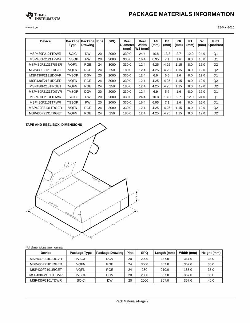
Device PackageType
PackageDrawing
Pins SPQ ReelDiameter
(mm)
ReelWidth
W1 (mm)
A0(mm)
B0(mm)
K0(mm)
P1(mm)
W(mm)
Pin1Quadrant
MSP430F2121TDWR SOIC DW 20 2000 330.0 24.4 10.8 13.3 2.7 12.0 24.0 Q1
MSP430F2121TPWR TSSOP PW 20 2000 330.0 16.4 6.95 7.1 1.6 8.0 16.0 Q1
MSP430F2121TRGER VQFN RGE 24 3000 330.0 12.4 4.25 4.25 1.15 8.0 12.0 Q2
MSP430F2121TRGET VQFN RGE 24 250 180.0 12.4 4.25 4.25 1.15 8.0 12.0 Q2
MSP430F2131IDGVR TVSOP DGV 20 2000 330.0 12.4 6.9 5.6 1.6 8.0 12.0 Q1
MSP430F2131IRGER VQFN RGE 24 3000 330.0 12.4 4.25 4.25 1.15 8.0 12.0 Q2
MSP430F2131IRGET VQFN RGE 24 250 180.0 12.4 4.25 4.25 1.15 8.0 12.0 Q2
MSP430F2131TDGVR TVSOP DGV 20 2000 330.0 12.4 6.9 5.6 1.6 8.0 12.0 Q1
MSP430F2131TDWR SOIC DW 20 2000 330.0 24.4 10.8 13.3 2.7 12.0 24.0 Q1
MSP430F2131TPWR TSSOP PW 20 2000 330.0 16.4 6.95 7.1 1.6 8.0 16.0 Q1
MSP430F2131TRGER VQFN RGE 24 3000 330.0 12.4 4.25 4.25 1.15 8.0 12.0 Q2
MSP430F2131TRGET VQFN RGE 24 250 180.0 12.4 4.25 4.25 1.15 8.0 12.0 Q2
*All dimensions are nominal
Device Package Type Package Drawing Pins SPQ Length (mm) Width (mm) Height (mm)
MSP430F2101IDGVR TVSOP DGV 20 2000 367.0 367.0 35.0
MSP430F2101IRGER VQFN RGE 24 3000 367.0 367.0 35.0
MSP430F2101IRGET VQFN RGE 24 250 210.0 185.0 35.0
MSP430F2101TDGVR TVSOP DGV 20 2000 367.0 367.0 35.0
MSP430F2101TDWR SOIC DW 20 2000 367.0 367.0 45.0
PACKAGE MATERIALS INFORMATION
www.ti.com 12-Mar-2016
Pack Materials-Page 2
Device Package Type Package Drawing Pins SPQ Length (mm) Width (mm) Height (mm)
MSP430F2101TPWR TSSOP PW 20 2000 367.0 367.0 38.0
MSP430F2101TRGER VQFN RGE 24 3000 367.0 367.0 35.0
MSP430F2111IDGVR TVSOP DGV 20 2000 367.0 367.0 35.0
MSP430F2111IRGER VQFN RGE 24 3000 367.0 367.0 35.0
MSP430F2111IRGET VQFN RGE 24 250 210.0 185.0 35.0
MSP430F2111TDGVR TVSOP DGV 20 2000 367.0 367.0 35.0
MSP430F2111TDWR SOIC DW 20 2000 367.0 367.0 45.0
MSP430F2111TRGER VQFN RGE 24 3000 367.0 367.0 35.0
MSP430F2111TRGET VQFN RGE 24 250 210.0 185.0 35.0
MSP430F2121IDGVR TVSOP DGV 20 2000 367.0 367.0 35.0
MSP430F2121IRGER VQFN RGE 24 3000 367.0 367.0 35.0
MSP430F2121IRGET VQFN RGE 24 250 210.0 185.0 35.0
MSP430F2121TDGVR TVSOP DGV 20 2000 367.0 367.0 35.0
MSP430F2121TDWR SOIC DW 20 2000 367.0 367.0 45.0
MSP430F2121TPWR TSSOP PW 20 2000 367.0 367.0 38.0
MSP430F2121TRGER VQFN RGE 24 3000 367.0 367.0 35.0
MSP430F2121TRGET VQFN RGE 24 250 210.0 185.0 35.0
MSP430F2131IDGVR TVSOP DGV 20 2000 367.0 367.0 35.0
MSP430F2131IRGER VQFN RGE 24 3000 367.0 367.0 35.0
MSP430F2131IRGET VQFN RGE 24 250 210.0 185.0 35.0
MSP430F2131TDGVR TVSOP DGV 20 2000 367.0 367.0 35.0
MSP430F2131TDWR SOIC DW 20 2000 367.0 367.0 45.0
MSP430F2131TPWR TSSOP PW 20 2000 367.0 367.0 38.0
MSP430F2131TRGER VQFN RGE 24 3000 367.0 367.0 35.0
MSP430F2131TRGET VQFN RGE 24 250 210.0 185.0 35.0
PACKAGE MATERIALS INFORMATION
www.ti.com 12-Mar-2016
Pack Materials-Page 3
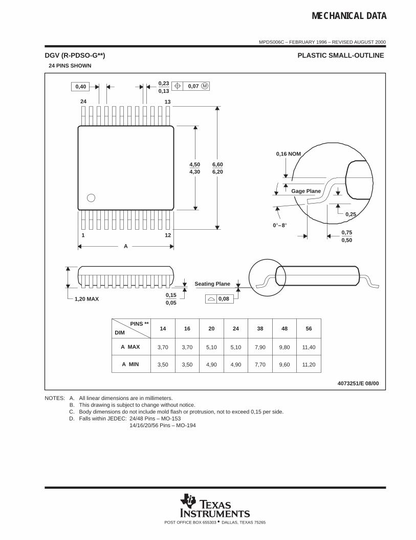
MECHANICAL DATA
MPDS006C – FEBRUARY 1996 – REVISED AUGUST 2000
POST OFFICE BOX 655303 • DALLAS, TEXAS 75265
DGV (R-PDSO-G**) PLASTIC SMALL-OUTLINE 24 PINS SHOWN
14
3,70
3,50 4,90
5,10
20DIM
PINS **
4073251/E 08/00
1,20 MAX
Seating Plane
0,050,15
0,25
0,500,75
0,230,13
1 12
24 13
4,304,50
0,16 NOM
Gage Plane
A
7,90
7,70
382416
4,90
5,103,70
3,50
A MAX
A MIN
6,606,20
11,20
11,40
56
9,60
9,80
48
0,08
M0,070,40
0°–8°
NOTES: A. All linear dimensions are in millimeters.B. This drawing is subject to change without notice.C. Body dimensions do not include mold flash or protrusion, not to exceed 0,15 per side.D. Falls within JEDEC: 24/48 Pins – MO-153
14/16/20/56 Pins – MO-194
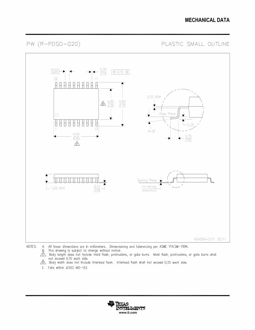
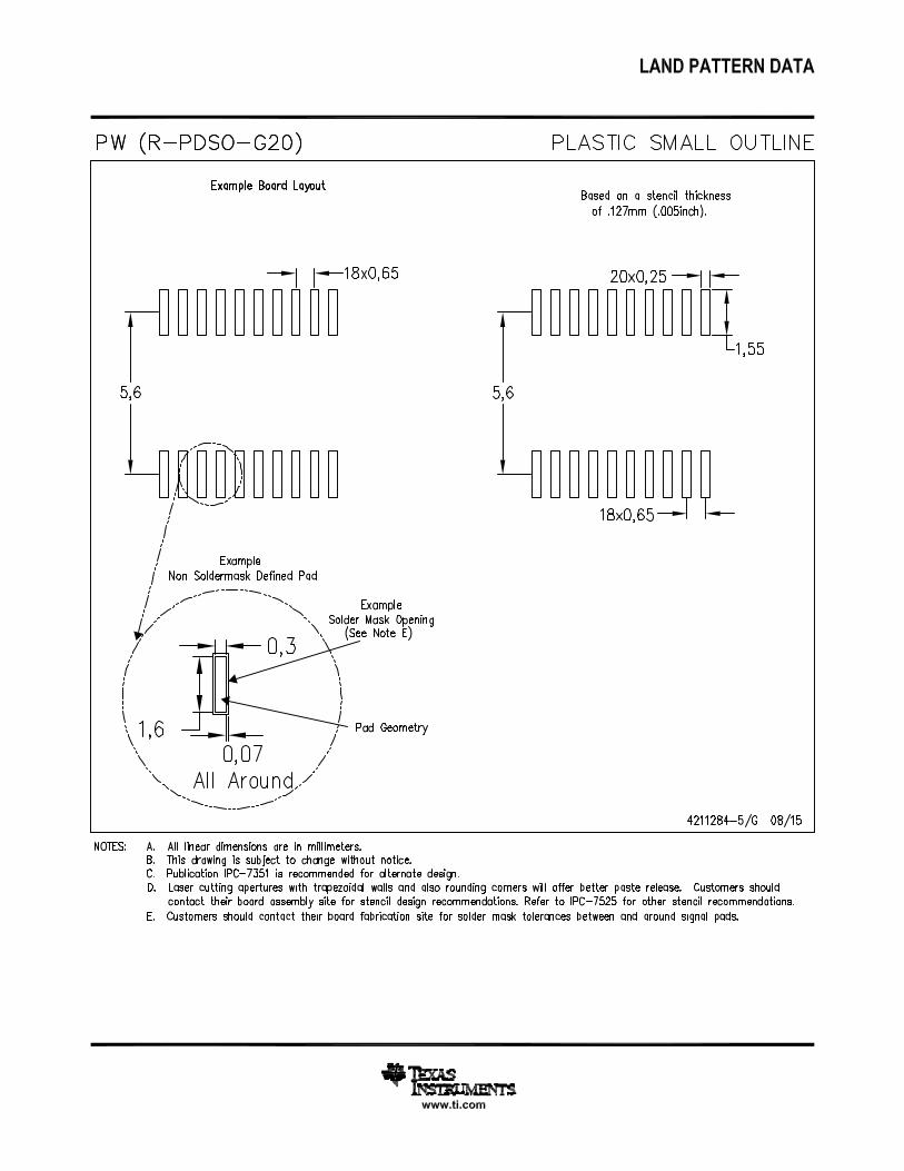
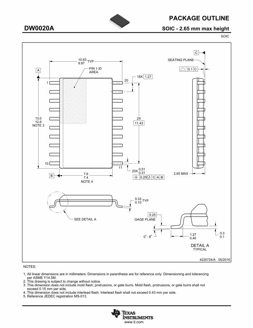
www.ti.com
PACKAGE OUTLINE
C
TYP10.639.97
2.65 MAX
18X 1.27
20X 0.510.31
2X11.43
TYP0.330.10
0 - 80.30.1
0.25GAGE PLANE
1.270.40
A
NOTE 3
13.012.6
B 7.67.4
4220724/A 05/2016
SOIC - 2.65 mm max heightDW0020ASOIC
NOTES: 1. All linear dimensions are in millimeters. Dimensions in parenthesis are for reference only. Dimensioning and tolerancing per ASME Y14.5M. 2. This drawing is subject to change without notice. 3. This dimension does not include mold flash, protrusions, or gate burrs. Mold flash, protrusions, or gate burrs shall not exceed 0.15 mm per side. 4. This dimension does not include interlead flash. Interlead flash shall not exceed 0.43 mm per side.5. Reference JEDEC registration MS-013.
120
0.25 C A B
1110
PIN 1 IDAREA
NOTE 4
SEATING PLANE
0.1 C
SEE DETAIL A
DETAIL ATYPICAL
SCALE 1.200
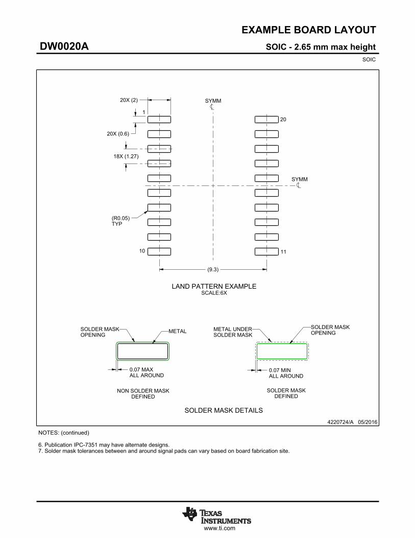
www.ti.com
EXAMPLE BOARD LAYOUT
(9.3)
0.07 MAXALL AROUND
0.07 MINALL AROUND
20X (2)
20X (0.6)
18X (1.27)
(R )TYP
0.05
4220724/A 05/2016
SOIC - 2.65 mm max heightDW0020ASOIC
SYMM
SYMM
LAND PATTERN EXAMPLESCALE:6X
1
10 11
20
NOTES: (continued) 6. Publication IPC-7351 may have alternate designs. 7. Solder mask tolerances between and around signal pads can vary based on board fabrication site.
METALSOLDER MASKOPENING
NON SOLDER MASKDEFINED
SOLDER MASK DETAILS
SOLDER MASKOPENING
METAL UNDERSOLDER MASK
SOLDER MASKDEFINED
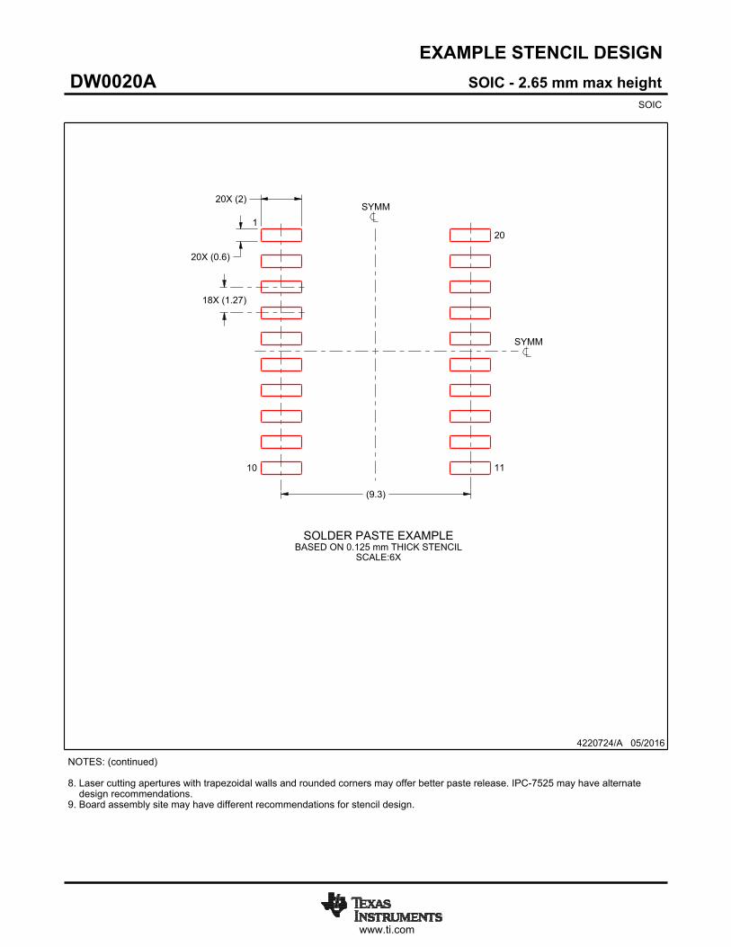
www.ti.com
EXAMPLE STENCIL DESIGN
(9.3)
18X (1.27)
20X (0.6)
20X (2)
4220724/A 05/2016
SOIC - 2.65 mm max heightDW0020ASOIC
NOTES: (continued) 8. Laser cutting apertures with trapezoidal walls and rounded corners may offer better paste release. IPC-7525 may have alternate design recommendations. 9. Board assembly site may have different recommendations for stencil design.
SYMM
SYMM
1
10 11
20
SOLDER PASTE EXAMPLEBASED ON 0.125 mm THICK STENCIL
SCALE:6X
GENERIC PACKAGE VIEW
Images above are just a representation of the package family, actual package may vary.Refer to the product data sheet for package details.
RGE 24 VQFN - 1 mm max heightPLASTIC QUAD FLATPACK - NO LEAD
4204104/H
www.ti.com
PACKAGE OUTLINE
C
SEE TERMINALDETAIL
24X 0.30.2
2.45 0.1
24X 0.50.3
1 MAX
(0.2) TYP
0.050.00
20X 0.5
2X2.5
2X 2.5
A 4.13.9
B
4.13.9
0.30.2
0.50.3
VQFN - 1 mm max heightRGE0024BPLASTIC QUAD FLATPACK - NO LEAD
4219013/A 05/2017
PIN 1 INDEX AREA
0.08 C
SEATING PLANE
1
6 13
18
7 12
24 19
(OPTIONAL)PIN 1 ID
0.1 C A B0.05
EXPOSEDTHERMAL PAD
25 SYMM
SYMM
NOTES: 1. All linear dimensions are in millimeters. Any dimensions in parenthesis are for reference only. Dimensioning and tolerancing per ASME Y14.5M. 2. This drawing is subject to change without notice. 3. The package thermal pad must be soldered to the printed circuit board for thermal and mechanical performance.
SCALE 3.000
DETAILOPTIONAL TERMINAL
TYPICAL
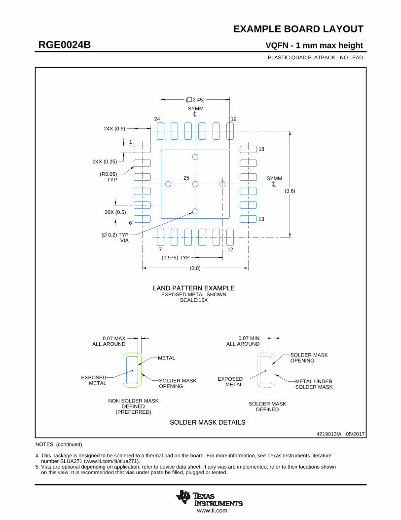
www.ti.com
EXAMPLE BOARD LAYOUT
0.07 MINALL AROUND
0.07 MAXALL AROUND
24X (0.25)
24X (0.6)
( 0.2) TYPVIA
20X (0.5)
(3.8)
(3.8)
( 2.45)
(R0.05)TYP
(0.975) TYP
VQFN - 1 mm max heightRGE0024BPLASTIC QUAD FLATPACK - NO LEAD
4219013/A 05/2017
SYMM
1
6
7 12
13
18
1924
SYMM
LAND PATTERN EXAMPLEEXPOSED METAL SHOWN
SCALE:15X
NOTES: (continued) 4. This package is designed to be soldered to a thermal pad on the board. For more information, see Texas Instruments literature number SLUA271 (www.ti.com/lit/slua271).5. Vias are optional depending on application, refer to device data sheet. If any vias are implemented, refer to their locations shown on this view. It is recommended that vias under paste be filled, plugged or tented.
25
SOLDER MASKOPENING
METAL UNDERSOLDER MASK
SOLDER MASKDEFINED
EXPOSEDMETAL
METAL
SOLDER MASKOPENING
SOLDER MASK DETAILS
NON SOLDER MASKDEFINED
(PREFERRED)
EXPOSEDMETAL
www.ti.com
EXAMPLE STENCIL DESIGN
24X (0.6)
24X (0.25)
20X (0.5)
(3.8)
(3.8)
4X ( 1.08)
(0.64)TYP
(0.64) TYP
(R0.05) TYP
VQFN - 1 mm max heightRGE0024BPLASTIC QUAD FLATPACK - NO LEAD
4219013/A 05/2017
NOTES: (continued) 6. Laser cutting apertures with trapezoidal walls and rounded corners may offer better paste release. IPC-7525 may have alternate design recommendations.
25
SYMM
METALTYP
SOLDER PASTE EXAMPLEBASED ON 0.125 mm THICK STENCIL
EXPOSED PAD 25
78% PRINTED SOLDER COVERAGE BY AREA UNDER PACKAGESCALE:20X
SYMM
1
6
7 12
13
18
1924
IMPORTANT NOTICE
Texas Instruments Incorporated (TI) reserves the right to make corrections, enhancements, improvements and other changes to itssemiconductor products and services per JESD46, latest issue, and to discontinue any product or service per JESD48, latest issue. Buyersshould obtain the latest relevant information before placing orders and should verify that such information is current and complete.TI’s published terms of sale for semiconductor products (http://www.ti.com/sc/docs/stdterms.htm) apply to the sale of packaged integratedcircuit products that TI has qualified and released to market. Additional terms may apply to the use or sale of other types of TI products andservices.Reproduction of significant portions of TI information in TI data sheets is permissible only if reproduction is without alteration and isaccompanied by all associated warranties, conditions, limitations, and notices. TI is not responsible or liable for such reproduceddocumentation. Information of third parties may be subject to additional restrictions. Resale of TI products or services with statementsdifferent from or beyond the parameters stated by TI for that product or service voids all express and any implied warranties for theassociated TI product or service and is an unfair and deceptive business practice. TI is not responsible or liable for any such statements.Buyers and others who are developing systems that incorporate TI products (collectively, “Designers”) understand and agree that Designersremain responsible for using their independent analysis, evaluation and judgment in designing their applications and that Designers havefull and exclusive responsibility to assure the safety of Designers' applications and compliance of their applications (and of all TI productsused in or for Designers’ applications) with all applicable regulations, laws and other applicable requirements. Designer represents that, withrespect to their applications, Designer has all the necessary expertise to create and implement safeguards that (1) anticipate dangerousconsequences of failures, (2) monitor failures and their consequences, and (3) lessen the likelihood of failures that might cause harm andtake appropriate actions. Designer agrees that prior to using or distributing any applications that include TI products, Designer willthoroughly test such applications and the functionality of such TI products as used in such applications.TI’s provision of technical, application or other design advice, quality characterization, reliability data or other services or information,including, but not limited to, reference designs and materials relating to evaluation modules, (collectively, “TI Resources”) are intended toassist designers who are developing applications that incorporate TI products; by downloading, accessing or using TI Resources in anyway, Designer (individually or, if Designer is acting on behalf of a company, Designer’s company) agrees to use any particular TI Resourcesolely for this purpose and subject to the terms of this Notice.TI’s provision of TI Resources does not expand or otherwise alter TI’s applicable published warranties or warranty disclaimers for TIproducts, and no additional obligations or liabilities arise from TI providing such TI Resources. TI reserves the right to make corrections,enhancements, improvements and other changes to its TI Resources. TI has not conducted any testing other than that specificallydescribed in the published documentation for a particular TI Resource.Designer is authorized to use, copy and modify any individual TI Resource only in connection with the development of applications thatinclude the TI product(s) identified in such TI Resource. NO OTHER LICENSE, EXPRESS OR IMPLIED, BY ESTOPPEL OR OTHERWISETO ANY OTHER TI INTELLECTUAL PROPERTY RIGHT, AND NO LICENSE TO ANY TECHNOLOGY OR INTELLECTUAL PROPERTYRIGHT OF TI OR ANY THIRD PARTY IS GRANTED HEREIN, including but not limited to any patent right, copyright, mask work right, orother intellectual property right relating to any combination, machine, or process in which TI products or services are used. Informationregarding or referencing third-party products or services does not constitute a license to use such products or services, or a warranty orendorsement thereof. Use of TI Resources may require a license from a third party under the patents or other intellectual property of thethird party, or a license from TI under the patents or other intellectual property of TI.TI RESOURCES ARE PROVIDED “AS IS” AND WITH ALL FAULTS. TI DISCLAIMS ALL OTHER WARRANTIES ORREPRESENTATIONS, EXPRESS OR IMPLIED, REGARDING RESOURCES OR USE THEREOF, INCLUDING BUT NOT LIMITED TOACCURACY OR COMPLETENESS, TITLE, ANY EPIDEMIC FAILURE WARRANTY AND ANY IMPLIED WARRANTIES OFMERCHANTABILITY, FITNESS FOR A PARTICULAR PURPOSE, AND NON-INFRINGEMENT OF ANY THIRD PARTY INTELLECTUALPROPERTY RIGHTS. TI SHALL NOT BE LIABLE FOR AND SHALL NOT DEFEND OR INDEMNIFY DESIGNER AGAINST ANY CLAIM,INCLUDING BUT NOT LIMITED TO ANY INFRINGEMENT CLAIM THAT RELATES TO OR IS BASED ON ANY COMBINATION OFPRODUCTS EVEN IF DESCRIBED IN TI RESOURCES OR OTHERWISE. IN NO EVENT SHALL TI BE LIABLE FOR ANY ACTUAL,DIRECT, SPECIAL, COLLATERAL, INDIRECT, PUNITIVE, INCIDENTAL, CONSEQUENTIAL OR EXEMPLARY DAMAGES INCONNECTION WITH OR ARISING OUT OF TI RESOURCES OR USE THEREOF, AND REGARDLESS OF WHETHER TI HAS BEENADVISED OF THE POSSIBILITY OF SUCH DAMAGES.Unless TI has explicitly designated an individual product as meeting the requirements of a particular industry standard (e.g., ISO/TS 16949and ISO 26262), TI is not responsible for any failure to meet such industry standard requirements.Where TI specifically promotes products as facilitating functional safety or as compliant with industry functional safety standards, suchproducts are intended to help enable customers to design and create their own applications that meet applicable functional safety standardsand requirements. Using products in an application does not by itself establish any safety features in the application. Designers mustensure compliance with safety-related requirements and standards applicable to their applications. Designer may not use any TI products inlife-critical medical equipment unless authorized officers of the parties have executed a special contract specifically governing such use.Life-critical medical equipment is medical equipment where failure of such equipment would cause serious bodily injury or death (e.g., lifesupport, pacemakers, defibrillators, heart pumps, neurostimulators, and implantables). Such equipment includes, without limitation, allmedical devices identified by the U.S. Food and Drug Administration as Class III devices and equivalent classifications outside the U.S.TI may expressly designate certain products as completing a particular qualification (e.g., Q100, Military Grade, or Enhanced Product).Designers agree that it has the necessary expertise to select the product with the appropriate qualification designation for their applicationsand that proper product selection is at Designers’ own risk. Designers are solely responsible for compliance with all legal and regulatoryrequirements in connection with such selection.Designer will fully indemnify TI and its representatives against any damages, costs, losses, and/or liabilities arising out of Designer’s non-compliance with the terms and provisions of this Notice.
Mailing Address: Texas Instruments, Post Office Box 655303, Dallas, Texas 75265Copyright © 2018, Texas Instruments Incorporated