Embed Size (px)
Citation preview
TN-29-05: ECC Module for Xilinx Spartan-3Overview
Technical NoteMicron® ECC Module for NAND Flash via Xilinx® Spartan™-3 FPGAFor detailed NAND Flash product information, see the 2Gb NAND Flash data sheet at www.micron.com/prod-ucts/nand/partlist.aspx.
OverviewNAND Flash devices have quickly become the preferred solution for high-density static memory storage, particularly in mobile product applications. As systems become capa-ble of accessing more and more memory space, larger amounts of data are stored and transferred both within systems and across networks. When storing and transferring large volumes of data, it is essential to detect and correct errors that may occur. Error correction code (ECC) fulfills this critical requirement.
The Micron® ECC module was developed and tested using Xilinx® Spartan™-3 and can be ported to certain other platforms of the user’s choosing.
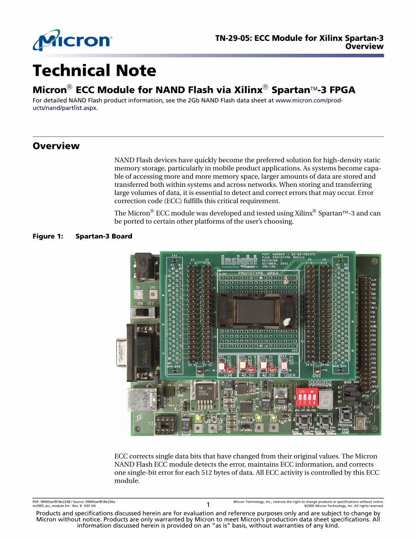
Figure 1: Spartan-3 Board
ECC corrects single data bits that have changed from their original values. The Micron NAND Flash ECC module detects the error, maintains ECC information, and corrects one single-bit error for each 512 bytes of data. All ECC activity is controlled by this ECC module.
PDF: 09005aef818e2248 / Source: 09005aef818e236a Micron Technology, Inc., reserves the right to change products or specifications without notice.tn2905_ecc_module.fm - Rev. B 5/07 EN 1 ©2005 Micron Technology, Inc. All rights reserved.
Products and specifications discussed herein are for evaluation and reference purposes only and are subject to change by Micron without notice. Products are only warranted by Micron to meet Micron’s production data sheet specifications. All
information discussed herein is provided on an “as is” basis, without warranties of any kind.
TN-29-05: ECC Module for Xilinx Spartan-3Micron ECC Module Configuration
In situations where the processor lacks a native NAND Flash controller, it is possible to design a simple memory-mapped interface. Where the memory-mapped design pro-vides a hardware interface to NAND, ECC is typically part of the application software and is not provided.
The ECC circuit described in this technical note is quite modest and in many cases could fit in a complex programmable logic device (CPLD) or in spare gates of a larger field-pro-grammable gate array (FPGA) already integral to the design.
The Micron ECC module supports all standard NAND Flash commands and will inter-rupt the host device communicating with the NAND Flash device upon error detection or correction. Utilizing the ECC module has no adverse impact on NAND Flash device performance. The ECC module can be altered by changing its model to support different ECC and data segment configurations.
This technical note describes the features of the Micron NAND Flash ECC module and how it calculates and implements ECC.
Micron ECC Module ConfigurationThe ECC module is designed to be placed between the NAND Flash device and the pro-cessor interface, as shown in Figure 2 on page 3. This processor interface can be a simple memory-mapped interface or a more complex controller requiring external or software ECC. The ECC module works in conjunction with the Micron NAND Flash controller to provide a glueless memory-mapped interface for nearly any host processor. The control-ler presents the NAND Flash device to the host processor as an SRAM interface. This supports a straightforward interface to the processor and minimizes the complexity of the NAND Flash interface.
Micron NAND Flash Controller
The NAND Flash controller is rated for a maximum clock speed of 100 MHz, with an asy-chronous 10ns access delay. For more information on the Micron NAND Flash control-ler, see technical note TN-29-06 at www.micron.com/products/nand/technotes.
PDF: 09005aef818e2248 / Source: 09005aef818e236a Micron Technology, Inc., reserves the right to change products or specifications without notice.tn2905_ecc_module.fm - Rev. B 5/07 EN 2 ©2005 Micron Technology, Inc. All rights reserved.
TN-29-05: ECC Module for Xilinx Spartan-3Micron ECC Module Configuration
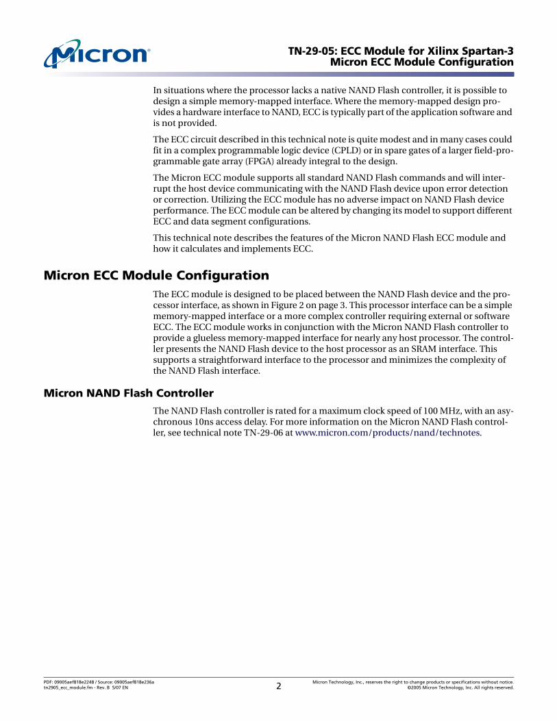
Figure 2: ECC Module Block Diagram
Note: I/F = interface.
Table 1: Pin Descriptions—Host Side
Symbol Type Pin Function
ALE Input These are standard NAND Flash interface pins. For detailed information, refer to the Micron NAND Flash data sheet.CE# Input
CLE Input
PRE Input
RE# Input
WE# Input
WP# Input
DATA [7:0] Bidirectional
R/B# Output The ready/busy# line is defined as busy when the NAND Flash part is busy or an ECC WRITE is in progress. Timing constraints for the R/B# pin are described in “READ Operation” and “WRITE Operation” on page 5 and “Write States” on page 12.
errINT Output This is the interrupt line. After a READ, if the ECC module finds an error, it takes the interrupt line HIGH for one clock cycle, signaling the controller that an error has been detected.
Error LocationModule
Hamming ECCError Locator(with Shift)
Hamming CodeGeneration
Module(with Registers)
NA
ND
ECC
Interface
NA
ND
ECC
Interface (w
ith o
r with
ou
t ECC
)
ECC FiniteControl Logic Module
HostCE#
HostCLE
HostALE
HostWE#
HostRE#
HostWP#
HostPRE
HostDATA[7:0]
HostR/B#
HosterrINT
CE#
CLE
ALE
WE#
RE#
WP#
PRE
DATA [7:0]
R/B#
ECC Module NANDDevice I/F
ProcessorI/F
PDF: 09005aef818e2248 / Source: 09005aef818e236a Micron Technology, Inc., reserves the right to change products or specifications without notice.tn2905_ecc_module.fm - Rev. B 5/07 EN 3 ©2005 Micron Technology, Inc. All rights reserved.
TN-29-05: ECC Module for Xilinx Spartan-3System Overview
System OverviewThe Micron ECC module is designed and implemented using the following hardware and software:• Xilinx® Spartan™-3 board• Memec Insight Prototype P160 board with 48-pin TSOP socket• Xilinx ISE™ 6.2i• Xilinx Platform Studio• Xilinx Impact• Xilinx XMD• ModelSim®
• Micron 2Gb NAND Flash device
ECC Scheme
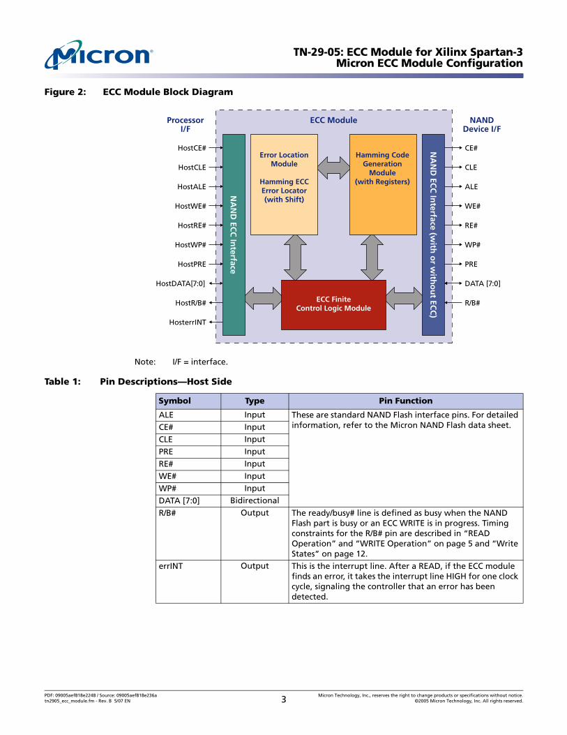
The NAND Flash ECC module implements a Hamming ECC scheme that can correct 1-bit errors and detect 2-bit errors in each 512-byte sector of the 2K NAND Flash page. The Hamming code uses 24 bits (3 bytes) of ECC information for each 512-byte sector, so 12 bytes of ECC encoding information is required per 2KB page. This ECC data is stored at the end of the 2,112-byte page (bytes 2,101–2,112); the controller can use the previous 52 bytes of extra space on each NAND Flash page. The ECC module does not calculate the ECC for the “spare” 52 bytes of information at the end of each page of the NAND blocks.
Together, the NAND Flash controller and the NAND ECC module provide a complete NAND Flash error management solution. This solution enables customers to easily incorporate NAND Flash devices without additional ECC considerations. Figure 3 depicts the ECC scheme.
Figure 3: Data/ECC Organization
1st 512 bytes 2nd 512 bytes 3rd 512 bytes 4th 512 bytes
SpareArea
Bytes2,049
to2,100
Byte 2,112
Byte 2,111
Byte 2,110
Byte 2,109
Byte 2,108
Byte 2,107
Byte 2,106
Byte 2,105
Byte 2,104
Byte 2,103
Byte 2,102
Byte 2,101
ECC for 1st512 bytes
ECC for 2nd512 bytes
ECC for 3rd512 bytes
ECC for 4th512 bytes
One NAND Flash page = 2,112 bytes
52 spare bytesnot used byECC module
PDF: 09005aef818e2248 / Source: 09005aef818e236a Micron Technology, Inc., reserves the right to change products or specifications without notice.tn2905_ecc_module.fm - Rev. B 5/07 EN 4 ©2005 Micron Technology, Inc. All rights reserved.
TN-29-05: ECC Module for Xilinx Spartan-3Working Description
Working Description
READ Operation
A READ operation with the ECC module needs to be initiated as a full-page READ for the ECC to be accurate. A full-page READ is necessary because the ECC is written to bytes 2,101–2,112. If the full-page READ is not executed, the controller cannot calculate the ECC for all four 512-byte sectors.
If a READ is initiated and the host tries to read byte 2,048, the ECC module pulls the R/B# line LOW, starts a READ in the ECC, and loads the ECC data into a shift register to calcu-late error locations when detectable errors are present. After this process is complete for the full-page READ, the R/B# line is pulled HIGH, and the host continues reading the remaining 52 data bytes by toggling the RE# line.
WRITE Operation
WRITEs initiated using the ECC module must be full-page WRITEs (2,112 bytes). This gives the ECC module time to calculate the ECC values for the whole page and write them to the correct locations. Similar to READs, after the host writes the 2,048th byte, the ECC module pulls the R/B# line LOW and starts writing the ECC into bytes 2,101 through 2,112. After this is complete and the R/B# line is HIGH again, the host continues to write the last 52 bytes.
NAND Flash Command Routing
All NAND Flash commands, such as READ ID, READ STATUS, RESET, and BLOCK ERASE, are piped directly to the NAND Flash device.
PDF: 09005aef818e2248 / Source: 09005aef818e236a Micron Technology, Inc., reserves the right to change products or specifications without notice.tn2905_ecc_module.fm - Rev. B 5/07 EN 5 ©2005 Micron Technology, Inc. All rights reserved.
TN-29-05: ECC Module for Xilinx Spartan-3Micron ECC Module Features and Characteristics
Micron ECC Module Features and Characteristics
Interface and Timing Specifications
The NAND Flash ECC module assumes that inputs are asynchronous, and, therefore, double registers are used to synchronize the inputs. If the inputs are synchronous, they can be passed through only one stage of latches. However, a single stage of latches is necessary because the control logic must evaluate the inputs before it can select the next state logic.
As inputs are passed through two register stages, outputs are delayed two clock cycles. This delay is inconsequential if clocking specifications are followed.
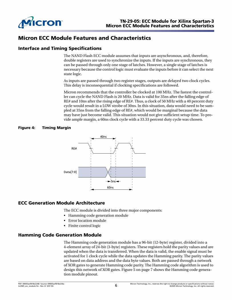
Micron recommends that the controller be clocked at 100 MHz. The fastest the control-ler can cycle the NAND Flash is 20 MHz. Data is valid for 35ns after the falling edge of RE# and 10ns after the rising edge of RE#. Thus, a clock of 50 MHz with a 40 percent duty cycle would result in a LOW strobe of 30ns. In this situation, data would need to be sam-pled at 35ns from the falling edge of RE#, which would be marginal because the data may have just become valid. This situation would not give sufficient setup time. To pro-vide ample margin, a 60ns clock cycle with a 33.33 percent duty cycle was chosen.
Figure 4: Timing Margin
ECC Generation Module Architecture
The ECC module is divided into three major components:• Hamming code generation module• Error location module• Finite control logic
Hamming Code Generation Module
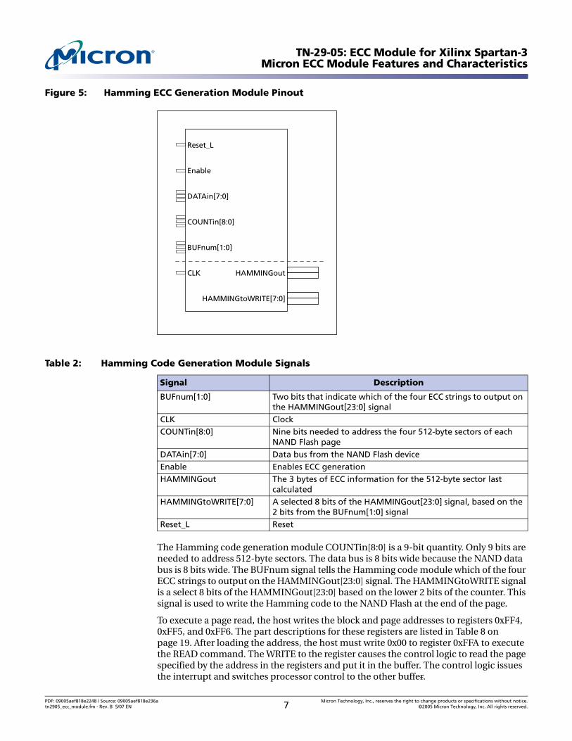
The Hamming code generation module has a 96-bit (12-byte) register, divided into a 4-element array of 24-bit (3-byte) registers. These registers hold the parity values and are updated when the data is transferred. When the data is valid, the enable signal must be activated for 1 clock cycle while the data updates the Hamming parity. The parity values are based on data address and the data byte values. Both are passed through a network of XOR gates to generate Hamming code parity. The Hamming code algorithm is used to design this network of XOR gates. Figure 5 on page 7 shows the Hamming code genera-tion module pinout.
40ns
60ns
5ns
RE#
Data[7:0]
PDF: 09005aef818e2248 / Source: 09005aef818e236a Micron Technology, Inc., reserves the right to change products or specifications without notice.tn2905_ecc_module.fm - Rev. B 5/07 EN 6 ©2005 Micron Technology, Inc. All rights reserved.
TN-29-05: ECC Module for Xilinx Spartan-3Micron ECC Module Features and Characteristics
Figure 5: Hamming ECC Generation Module Pinout
The Hamming code generation module COUNTin[8:0] is a 9-bit quantity. Only 9 bits are needed to address 512-byte sectors. The data bus is 8 bits wide because the NAND data bus is 8 bits wide. The BUFnum signal tells the Hamming code module which of the four ECC strings to output on the HAMMINGout[23:0] signal. The HAMMINGtoWRITE signal is a select 8 bits of the HAMMINGout[23:0] based on the lower 2 bits of the counter. This signal is used to write the Hamming code to the NAND Flash at the end of the page.
To execute a page read, the host writes the block and page addresses to registers 0xFF4, 0xFF5, and 0xFF6. The part descriptions for these registers are listed in Table 8 on page 19. After loading the address, the host must write 0x00 to register 0xFFA to execute the READ command. The WRITE to the register causes the control logic to read the page specified by the address in the registers and put it in the buffer. The control logic issues the interrupt and switches processor control to the other buffer.
Table 2: Hamming Code Generation Module Signals
Signal Description
BUFnum[1:0] Two bits that indicate which of the four ECC strings to output on the HAMMINGout[23:0] signal
CLK ClockCOUNTin[8:0] Nine bits needed to address the four 512-byte sectors of each
NAND Flash pageDATAin[7:0] Data bus from the NAND Flash deviceEnable Enables ECC generationHAMMINGout The 3 bytes of ECC information for the 512-byte sector last
calculatedHAMMINGtoWRITE[7:0] A selected 8 bits of the HAMMINGout[23:0] signal, based on the
2 bits from the BUFnum[1:0] signalReset_L Reset
Reset_L
Enable
DATAin[7:0]
COUNTin[8:0]
BUFnum[1:0]
CLK HAMMINGout
HAMMINGtoWRITE[7:0]
PDF: 09005aef818e2248 / Source: 09005aef818e236a Micron Technology, Inc., reserves the right to change products or specifications without notice.tn2905_ecc_module.fm - Rev. B 5/07 EN 7 ©2005 Micron Technology, Inc. All rights reserved.
TN-29-05: ECC Module for Xilinx Spartan-3Micron ECC Module Features and Characteristics
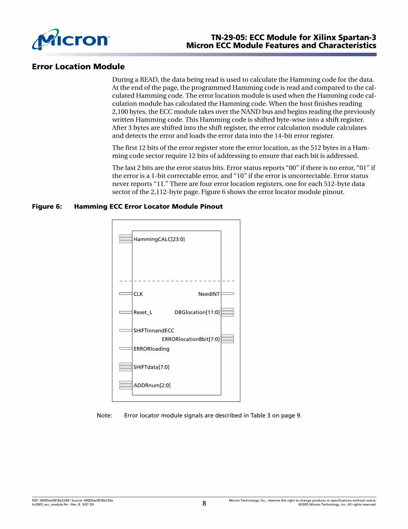
Error Location Module
During a READ, the data being read is used to calculate the Hamming code for the data. At the end of the page, the programmed Hamming code is read and compared to the cal-culated Hamming code. The error location module is used when the Hamming code cal-culation module has calculated the Hamming code. When the host finishes reading 2,100 bytes, the ECC module takes over the NAND bus and begins reading the previously written Hamming code. This Hamming code is shifted byte-wise into a shift register. After 3 bytes are shifted into the shift register, the error calculation module calculates and detects the error and loads the error data into the 14-bit error register.
The first 12 bits of the error register store the error location, as the 512 bytes in a Ham-ming code sector require 12 bits of addressing to ensure that each bit is addressed.
The last 2 bits are the error status bits. Error status reports “00” if there is no error, “01” if the error is a 1-bit correctable error, and “10” if the error is uncorrectable. Error status never reports “11.” There are four error location registers, one for each 512-byte data sector of the 2,112-byte page. Figure 6 shows the error locator module pinout.
Figure 6: Hamming ECC Error Locator Module Pinout
Note: Error locator module signals are described in Table 3 on page 9.
HammingCALC[23:0]
CLK
Reset_L
SHIFTinnandECC
ERRORloading
SHIFTdata[7:0]
ADDRnum[2:0]
NeedINT
DBGlocation[11:0]
ERRORlocation8bit[7:0]
PDF: 09005aef818e2248 / Source: 09005aef818e236a Micron Technology, Inc., reserves the right to change products or specifications without notice.tn2905_ecc_module.fm - Rev. B 5/07 EN 8 ©2005 Micron Technology, Inc. All rights reserved.
TN-29-05: ECC Module for Xilinx Spartan-3Micron ECC Module Features and Characteristics
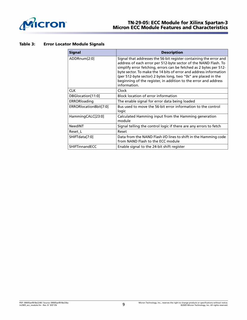
Table 3: Error Locator Module Signals
Signal Description
ADDRnum[2:0] Signal that addresses the 56-bit register containing the error and address of each error per 512-byte sector of the NAND Flash. To simplify error fetching, errors can be fetched as 2 bytes per 512-byte sector. To make the 14 bits of error and address information (per 512-byte sector) 2 bytes long, two “0s” are placed in the beginning of the register, in addition to the error and address information.
CLK ClockDBGlocation[11:0] Block location of error informationERRORloading The enable signal for error data being loadedERRORlocation8bit[7:0] Bus used to move the 56-bit error information to the control
logicHammingCALC[23:0] Calculated Hamming input from the Hamming generation
moduleNeedINT Signal telling the control logic if there are any errors to fetchReset_L ResetSHIFTdata[7:0] Data from the NAND Flash I/O lines to shift in the Hamming code
from NAND Flash to the ECC moduleSHIFTinnandECC Enable signal to the 24-bit shift register
PDF: 09005aef818e2248 / Source: 09005aef818e236a Micron Technology, Inc., reserves the right to change products or specifications without notice.tn2905_ecc_module.fm - Rev. B 5/07 EN 9 ©2005 Micron Technology, Inc. All rights reserved.
TN-29-05: ECC Module for Xilinx Spartan-3Micron ECC Module Features and Characteristics
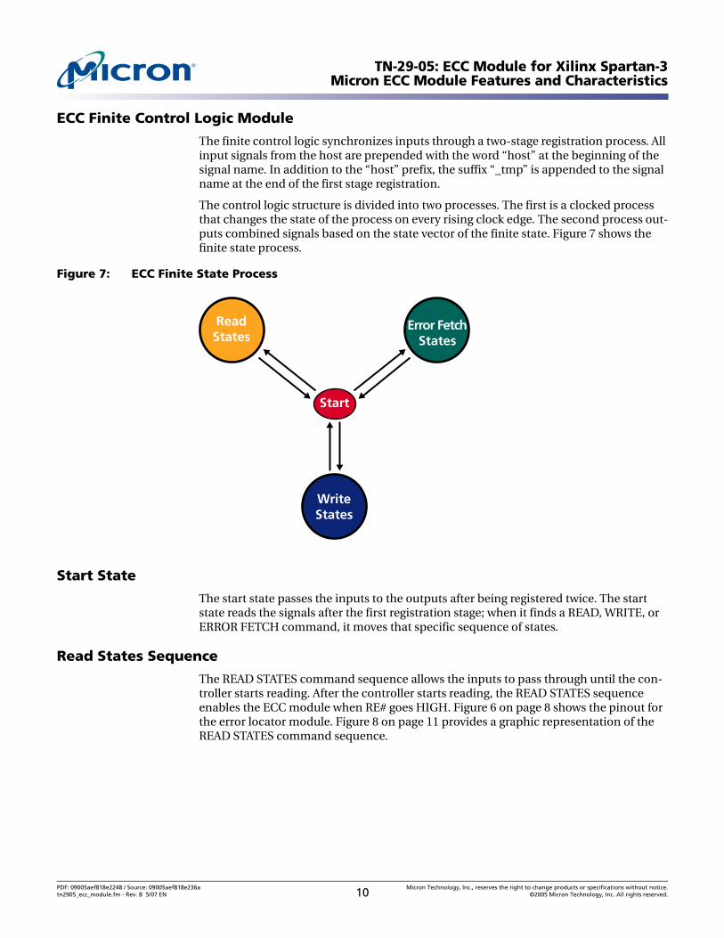
ECC Finite Control Logic Module
The finite control logic synchronizes inputs through a two-stage registration process. All input signals from the host are prepended with the word “host” at the beginning of the signal name. In addition to the “host” prefix, the suffix “_tmp” is appended to the signal name at the end of the first stage registration.
The control logic structure is divided into two processes. The first is a clocked process that changes the state of the process on every rising clock edge. The second process out-puts combined signals based on the state vector of the finite state. Figure 7 shows the finite state process.
Figure 7: ECC Finite State Process
Start State
The start state passes the inputs to the outputs after being registered twice. The start state reads the signals after the first registration stage; when it finds a READ, WRITE, or ERROR FETCH command, it moves that specific sequence of states.
Read States Sequence
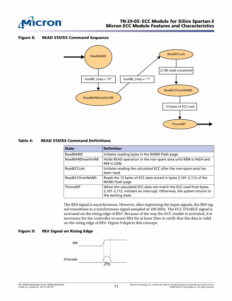
The READ STATES command sequence allows the inputs to pass through until the con-troller starts reading. After the controller starts reading, the READ STATES sequence enables the ECC module when RE# goes HIGH. Figure 6 on page 8 shows the pinout for the error locator module. Figure 8 on page 11 provides a graphic representation of the READ STATES command sequence.
Start
Error FetchStates
ReadStates
WriteStates
PDF: 09005aef818e2248 / Source: 09005aef818e236a Micron Technology, Inc., reserves the right to change products or specifications without notice.tn2905_ecc_module.fm - Rev. B 5/07 EN 10 ©2005 Micron Technology, Inc. All rights reserved.
TN-29-05: ECC Module for Xilinx Spartan-3Micron ECC Module Features and Characteristics
Figure 8: READ STATES Command Sequence
The RE# signal is asynchronous. However, after registering the input signals, the RE# sig-nal transitions to a synchronous signal sampled at 100 MHz. The ECC ENABLE signal is activated on the rising edge of RE#. Because of the way the ECC enable is activated, it is necessary for the controller to assert RE# for at least 35ns to verify that the data is valid on the rising edge of RE#. Figure 9 depicts this concept.
Figure 9: RE# Signal on Rising Edge
Table 4: READ STATES Command Definitions
State Definition
ReadNAND Initiates reading bytes in the NAND Flash page.ReadNANDwaitforRB Holds READ operation in the non-spare area until R/B# is HIGH and
RE# is LOW.ReadECCcalc Initiates reading the calculated ECC after the non-spare area has
been read.ReadECCfromNAND Reads the 12 bytes of ECC data stored in bytes 2,101–2,112 of the
NAND Flash page.ThrowINT When the calculated ECC does not match the ECC read from bytes
2,101–2,112, initiates an interrupt. Otherwise, the system returns to the starting state.
ReadNAND
hostRB_Ltmp = “0” hostRB_Ltmp = “1”
ReadNANDwaitforRB
ReadECCcalc
2,100 reads completed
ReadECCfromNAND
12 bytes of ECC read
ThrowINT
10ns
RE#
ECCenable
PDF: 09005aef818e2248 / Source: 09005aef818e236a Micron Technology, Inc., reserves the right to change products or specifications without notice.tn2905_ecc_module.fm - Rev. B 5/07 EN 11 ©2005 Micron Technology, Inc. All rights reserved.
TN-29-05: ECC Module for Xilinx Spartan-3Micron ECC Module Features and Characteristics
The ThrowINT state fires a 10ns signal alerting the host that an error has occurred and requires correction. The 10ns signal is fired based on the arrival of a NeedINT signal from the error locator module.
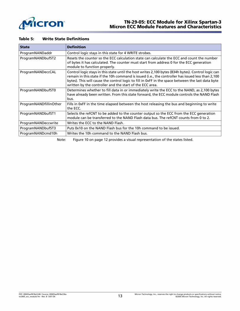
Write States
Write states comprise a linear set of states. It is important to note that the ECC module only supports full-page WRITEs. The state transition conditions are based on the num-ber of cycles for which the control logic will remain in a given state. During a READ oper-ation, after the address and command are issued, R/B# goes LOW before data can be output. This READ sequence differs from the WRITE sequence in that the READ sequence outputs data following a CONFIRM (10h) command for R/B# to go LOW.
Figure 10: Write States Flow
Note: Write-state definitions are provided in Table 5 on page 13.
ProgramNAND
ProgramNANDfillinOther
ProgramNANDbufST1
ProgramNANDeccwrite
ProgramNANDbufST3
ProgramNANDcmd10h
hostALE_Htmp = “1”
ProgramNANDaddr
hostALE_H_tmp = “0” andinternal_COUNT > x “004”
ProgramNANDbufST2
ProgramNANDeccCAL
ProgramNANDbufST0
internal_COUNT > x “833”
internal_COUNT > x “833”
internal_COUNT < x “833”
internal_COUNT > x “83F”
internal_COUNT > x “833”or the 10h command is issued
PDF: 09005aef818e2248 / Source: 09005aef818e236a Micron Technology, Inc., reserves the right to change products or specifications without notice.tn2905_ecc_module.fm - Rev. B 5/07 EN 12 ©2005 Micron Technology, Inc. All rights reserved.
TN-29-05: ECC Module for Xilinx Spartan-3Micron ECC Module Features and Characteristics
Note: Figure 10 on page 12 provides a visual representation of the states listed.
Table 5: Write State Definitions
State Definition
ProgramNANDaddr Control logic stays in this state for 4 WRITE strobes.ProgramNANDbufST2 Resets the counter so the ECC calculation state can calculate the ECC and count the number
of bytes it has calculated. The counter must start from address 0 for the ECC generation module to function properly.
ProgramNANDeccCAL Control logic stays in this state until the host writes 2,100 bytes (834h bytes). Control logic can remain in this state if the 10h command is issued (i.e., the controller has issued less than 2,100 bytes). This will cause the control logic to fill in 0xFF in the space between the last data byte written by the controller and the start of the ECC area.
ProgramNANDbufST0 Determines whether to fill data in or immediately write the ECC to the NAND, as 2,100 bytes have already been written. From this state forward, the ECC module controls the NAND Flash bus.
ProgramNANDfillinOther Fills in 0xFF in the time elapsed between the host releasing the bus and beginning to write the ECC.
ProgramNANDbufST1 Selects the refCNT to be added to the counter output so the ECC from the ECC generation module can be transferred to the NAND Flash data bus. The refCNT counts from 0 to 2.
ProgramNANDeccwrite Writes the ECC to the NAND Flash.ProgramNANDbufST3 Puts 0x10 on the NAND Flash bus for the 10h command to be issued.ProgramNANDcmd10h Writes the 10h command to the NAND Flash bus.
PDF: 09005aef818e2248 / Source: 09005aef818e236a Micron Technology, Inc., reserves the right to change products or specifications without notice.tn2905_ecc_module.fm - Rev. B 5/07 EN 13 ©2005 Micron Technology, Inc. All rights reserved.
TN-29-05: ECC Module for Xilinx Spartan-3Micron ECC Module Features and Characteristics
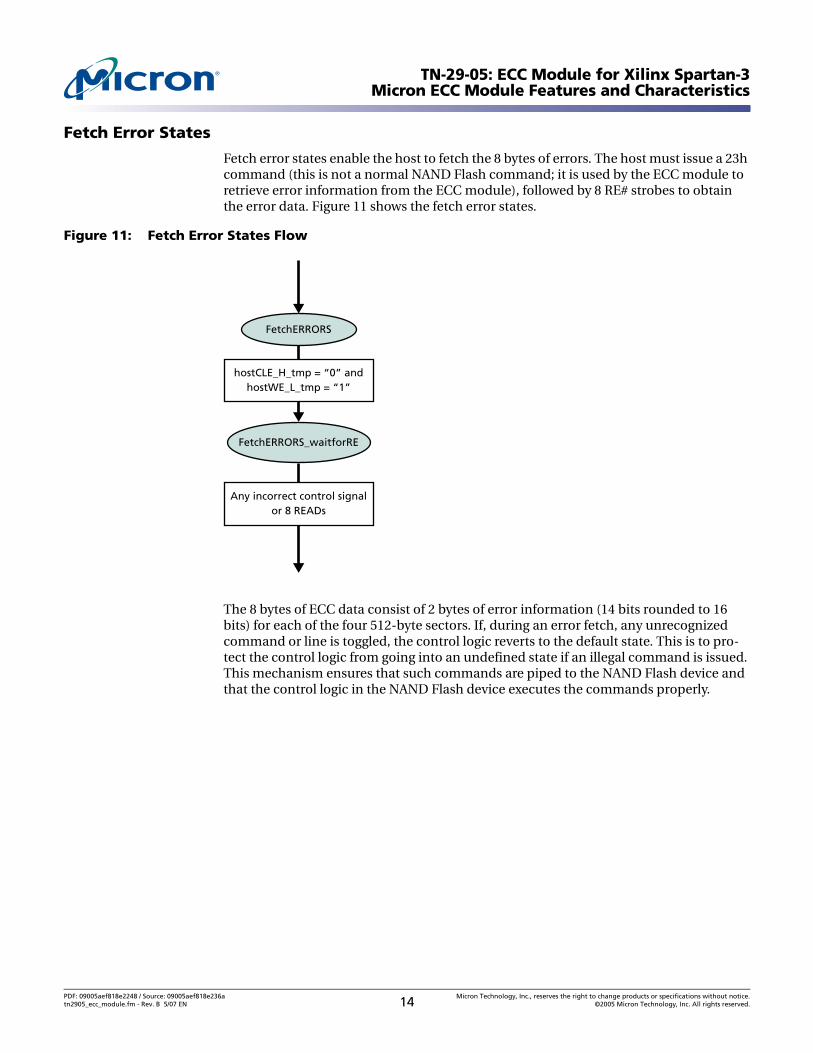
Fetch Error States
Fetch error states enable the host to fetch the 8 bytes of errors. The host must issue a 23h command (this is not a normal NAND Flash command; it is used by the ECC module to retrieve error information from the ECC module), followed by 8 RE# strobes to obtain the error data. Figure 11 shows the fetch error states.
Figure 11: Fetch Error States Flow
The 8 bytes of ECC data consist of 2 bytes of error information (14 bits rounded to 16 bits) for each of the four 512-byte sectors. If, during an error fetch, any unrecognized command or line is toggled, the control logic reverts to the default state. This is to pro-tect the control logic from going into an undefined state if an illegal command is issued. This mechanism ensures that such commands are piped to the NAND Flash device and that the control logic in the NAND Flash device executes the commands properly.
FetchERRORS
FetchERRORS_waitforRE
Any incorrect control signalor 8 READs
hostCLE_H_tmp = “0” andhostWE_L_tmp = “1”
PDF: 09005aef818e2248 / Source: 09005aef818e236a Micron Technology, Inc., reserves the right to change products or specifications without notice.tn2905_ecc_module.fm - Rev. B 5/07 EN 14 ©2005 Micron Technology, Inc. All rights reserved.
TN-29-05: ECC Module for Xilinx Spartan-3ECC Hamming Code Algorithm
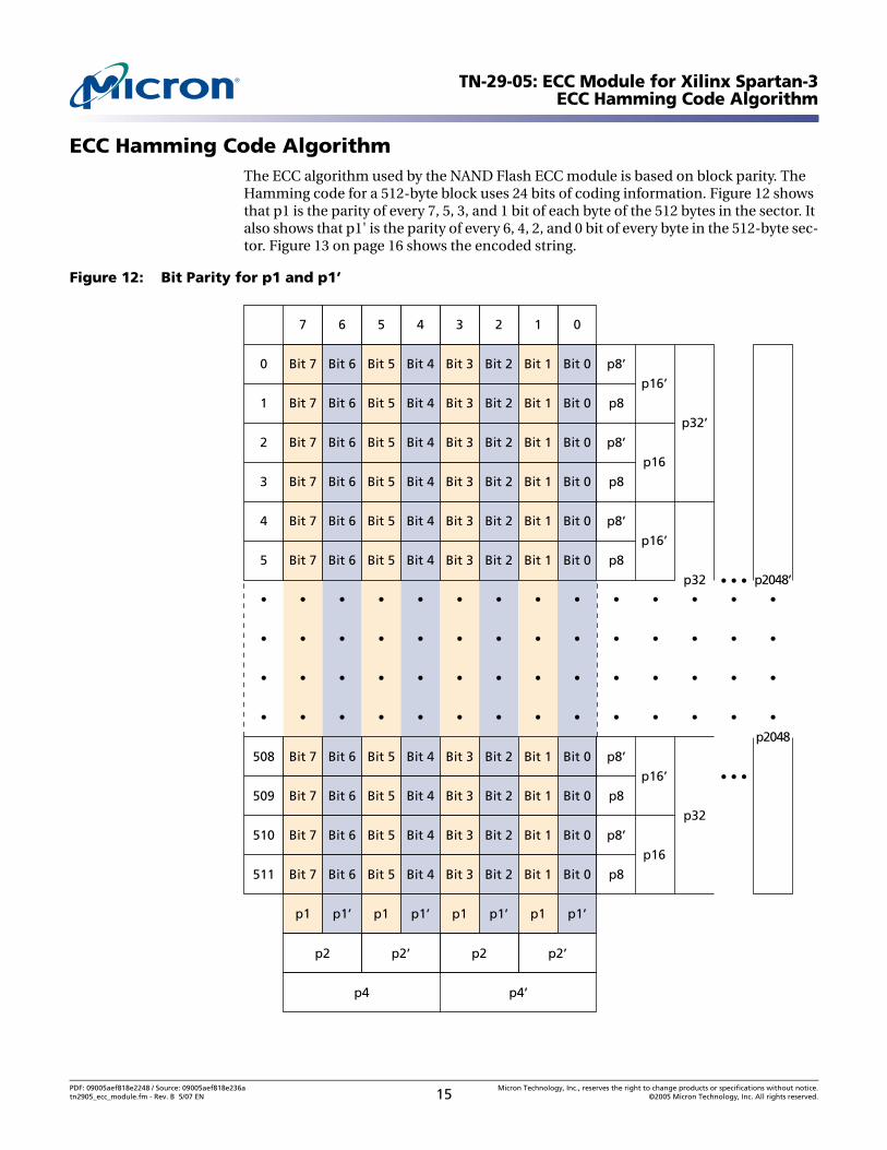
ECC Hamming Code AlgorithmThe ECC algorithm used by the NAND Flash ECC module is based on block parity. The Hamming code for a 512-byte block uses 24 bits of coding information. Figure 12 shows that p1 is the parity of every 7, 5, 3, and 1 bit of each byte of the 512 bytes in the sector. It also shows that p1' is the parity of every 6, 4, 2, and 0 bit of every byte in the 512-byte sec-tor. Figure 13 on page 16 shows the encoded string.
Figure 12: Bit Parity for p1 and p1’
0
1
2
3
4
5
•
•
•
•
508
509
510
511
p8’
p8
p8’
p8
p8’
p8
•
•
•
•
p8’
p8
p8’
p8
•
•
•
•
•
•
•
•
•
•
•
•
•
•
•
•
p16’
p16
p16’
p16’
p16
p32’
p32
p32
p2048’
p2048
p2
p4 p4’
p2’ p2 p2’
7
Bit 7
Bit 7
Bit 7
Bit 7
Bit 7
Bit 7
•
•
•
•
Bit 7
Bit 7
Bit 7
Bit 7
p1
6
Bit 6
Bit 6
Bit 6
Bit 6
Bit 6
Bit 6
•
•
•
•
Bit 6
Bit 6
Bit 6
Bit 6
p1’
5
Bit 5
Bit 5
Bit 5
Bit 5
Bit 5
Bit 5
•
•
•
•
Bit 5
Bit 5
Bit 5
Bit 5
p1
4
Bit 4
Bit 4
Bit 4
Bit 4
Bit 4
Bit 4
•
•
•
•
Bit 4
Bit 4
Bit 4
Bit 4
p1’
3
Bit 3
Bit 3
Bit 3
Bit 3
Bit 3
Bit 3
•
•
•
•
Bit 3
Bit 3
Bit 3
Bit 3
p1
2
Bit 2
Bit 2
Bit 2
Bit 2
Bit 2
Bit 2
•
•
•
•
Bit 2
Bit 2
Bit 2
Bit 2
p1’
1
Bit 1
Bit 1
Bit 1
Bit 1
Bit 1
Bit 1
•
•
•
•
Bit 1
Bit 1
Bit 1
Bit 1
p1
0
Bit 0
Bit 0
Bit 0
Bit 0
Bit 0
Bit 0
•
•
•
•
Bit 0
Bit 0
Bit 0
Bit 0
p1’
• • •
• • •
PDF: 09005aef818e2248 / Source: 09005aef818e236a Micron Technology, Inc., reserves the right to change products or specifications without notice.tn2905_ecc_module.fm - Rev. B 5/07 EN 15 ©2005 Micron Technology, Inc. All rights reserved.
TN-29-05: ECC Module for Xilinx Spartan-3ECC Hamming Code Algorithm
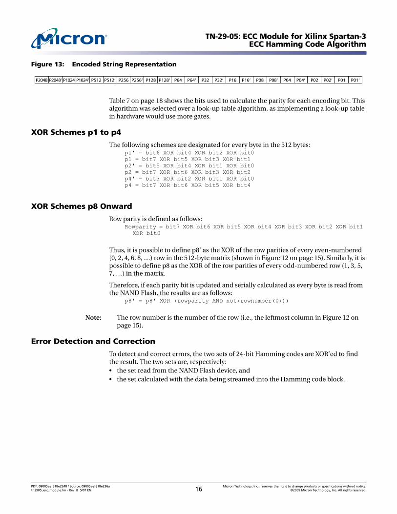
Figure 13: Encoded String Representation
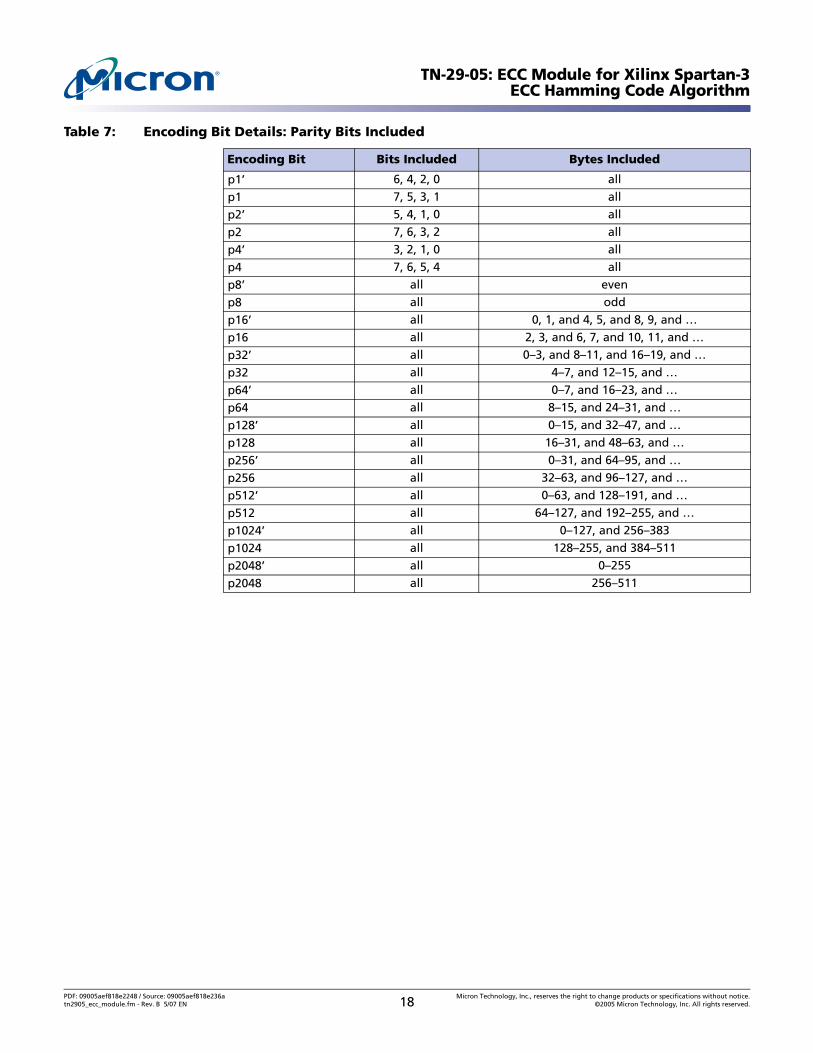
Table 7 on page 18 shows the bits used to calculate the parity for each encoding bit. This algorithm was selected over a look-up table algorithm, as implementing a look-up table in hardware would use more gates.
XOR Schemes p1 to p4
The following schemes are designated for every byte in the 512 bytes:p1' = bit6 XOR bit4 XOR bit2 XOR bit0p1 = bit7 XOR bit5 XOR bit3 XOR bit1p2' = bit5 XOR bit4 XOR bit1 XOR bit0p2 = bit7 XOR bit6 XOR bit3 XOR bit2 p4' = bit3 XOR bit2 XOR bit1 XOR bit0p4 = bit7 XOR bit6 XOR bit5 XOR bit4
XOR Schemes p8 Onward
Row parity is defined as follows:Rowparity = bit7 XOR bit6 XOR bit5 XOR bit4 XOR bit3 XOR bit2 XOR bit1
XOR bit0
Thus, it is possible to define p8' as the XOR of the row parities of every even-numbered (0, 2, 4, 6, 8, …) row in the 512-byte matrix (shown in Figure 12 on page 15). Similarly, it is possible to define p8 as the XOR of the row parities of every odd-numbered row (1, 3, 5, 7, …) in the matrix.
Therefore, if each parity bit is updated and serially calculated as every byte is read from the NAND Flash, the results are as follows:
p8' = p8' XOR (rowparity AND not(rownumber(0)))
Note: The row number is the number of the row (i.e., the leftmost column in Figure 12 on page 15).
Error Detection and Correction
To detect and correct errors, the two sets of 24-bit Hamming codes are XOR’ed to find the result. The two sets are, respectively:• the set read from the NAND Flash device, and• the set calculated with the data being streamed into the Hamming code block.
P2048’P2048 P1024 P1024’ P512 P512’ P256 P256’ P128 P128’ P64 P64’ P32 P32’ P16 P16’ P08 P08’ P04 P04’ P02 P02’ P01 P01’
PDF: 09005aef818e2248 / Source: 09005aef818e236a Micron Technology, Inc., reserves the right to change products or specifications without notice.tn2905_ecc_module.fm - Rev. B 5/07 EN 16 ©2005 Micron Technology, Inc. All rights reserved.
TN-29-05: ECC Module for Xilinx Spartan-3ECC Hamming Code Algorithm
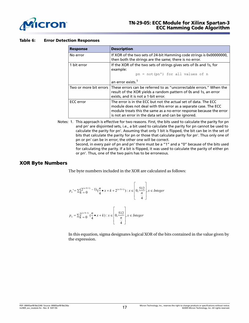
Notes: 1. This approach is effective for two reasons. First, the bits used to calculate the parity for pn and pn' are disjointed sets, i.e., a bit used to calculate the parity for pn cannot be used to calculate the parity for pn'. Assuming that only 1 bit is flipped, the bit can be in the set of bits that calculate the parity for pn or those that calculate parity for pn'. Thus only one of pn or pn' can be in error; the other one will be correct.Second, in every pair of pn and pn' there must be a “1” and a “0” because of the bits used for calculating the parity. If a bit is flipped, it was used to calculate the parity of either pn or pn'. Thus, one of the two pairs has to be erroneous.
XOR Byte Numbers
The byte numbers included in the XOR are calculated as follows:
In this equation, sigma designates logical XOR of the bits contained in the value given by the expression.
Table 6: Error Detection Responses
Response Description
No error If XOR of the two sets of 24-bit Hamming code strings is 0x00000000, then both the strings are the same; there is no error.
1 bit error If the XOR of the two sets of strings gives sets of 0s and 1s, for example:
pn = not(pn') for all values of n
an error exists.1
Two or more bit errors These errors can be referred to as “uncorrectable errors.” When the result of the XOR yields a random pattern of 0s and 1s, an error exists, and it is not a 1-bit error.
ECC error The error is in the ECC but not the actual set of data. The ECC module does not deal with this error as a separate case. The ECC module treats this the same as a no-error response because the error is not an error in the data set and can be ignored.
Integerxk nxkxnpn n
n ∈∑ −=
⎥⎥⎥
⎦
⎤
⎢⎢⎢
⎣
⎡
∈++•=− − ,)12(0
4
512,0:)24('
)18/( )18/(
Integerxk nxkxnpn
n ∈∑ =⎥⎥⎥
⎦
⎤
⎢⎢⎢
⎣
⎡
∈+•=−
,20
4
512,0:)4()18/(
PDF: 09005aef818e2248 / Source: 09005aef818e236a Micron Technology, Inc., reserves the right to change products or specifications without notice.tn2905_ecc_module.fm - Rev. B 5/07 EN 17 ©2005 Micron Technology, Inc. All rights reserved.
TN-29-05: ECC Module for Xilinx Spartan-3ECC Hamming Code Algorithm
Table 7: Encoding Bit Details: Parity Bits Included
Encoding Bit Bits Included Bytes Included
p1’ 6, 4, 2, 0 all
p1 7, 5, 3, 1 all
p2’ 5, 4, 1, 0 all
p2 7, 6, 3, 2 all
p4’ 3, 2, 1, 0 all
p4 7, 6, 5, 4 all
p8’ all even
p8 all odd
p16’ all 0, 1, and 4, 5, and 8, 9, and …
p16 all 2, 3, and 6, 7, and 10, 11, and …
p32’ all 0–3, and 8–11, and 16–19, and …
p32 all 4–7, and 12–15, and …
p64’ all 0–7, and 16–23, and …
p64 all 8–15, and 24–31, and …
p128’ all 0–15, and 32–47, and …
p128 all 16–31, and 48–63, and …
p256’ all 0–31, and 64–95, and …
p256 all 32–63, and 96–127, and …
p512’ all 0–63, and 128–191, and …
p512 all 64–127, and 192–255, and …
p1024’ all 0–127, and 256–383
p1024 all 128–255, and 384–511
p2048’ all 0–255
p2048 all 256–511
PDF: 09005aef818e2248 / Source: 09005aef818e236a Micron Technology, Inc., reserves the right to change products or specifications without notice.tn2905_ecc_module.fm - Rev. B 5/07 EN 18 ©2005 Micron Technology, Inc. All rights reserved.
TN-29-05: ECC Module for Xilinx Spartan-3ECC Hamming Code Algorithm
Read Error Locations
To read the error locations, the host must issue command AAh to the ECC module exactly the same way a NAND Flash command is issued. The host then strobes RE# eight times to retrieve the 8 bytes of error information. The format of the error information is described in Table 8.
Note: Only 12 bits of information are required to locate an error in a 512-byte sector, as the 512-byte sector has 212 = 4,096 bits.
Table 8: Error Location Byte Descriptions
Byte Read
Byte Description
Bit 7 Bit 6 Bit 5 Bit 4 Bit 3 Bit 2 Bit 1 Bit 0
Byte 0 First 512-byte
sector
Error location
bit 7
Error location
bit 6
Error location
bit 5
Error location
bit 4
Error location
bit 3
Error location
bit 2
Error location
bit 1
Error location
bit 0Byte 1 0 0 Error status
bit 0Error status
bit 0Error
locationbit 11
Error locationbit 10
Error location
bit 9
Error location
bit 8Byte 2 Second
512-byte sector
Error location
bit 7
Error location
bit 6
Error location
bit 5
Error location
bit 4
Error location
bit 3
Error location
bit 2
Error location
bit 1
Error location
bit 0Byte 3 0 0 Error status
bit 0Error status
bit 0Error
locationbit 11
Error locationbit 10
Error location
bit 9
Error location
bit 8Byte 4
3rd 512- byte
sector
Error location
bit 7
Error location
bit 6
Error location
bit 5
Error location
bit 4
Error location
bit 3
Error location
bit 2
Error location
bit 1
Error location
bit 0Byte 5 0 0 Error status
bit 0Error status
bit 0 Error
locationbit 11
Error locationbit 10
Error location
bit 9
Error location
bit 8Byte 6
4th 512- byte
sector
Error location
bit 7
Error location
bit 6
Error location
bit 5
Error location
bit 4
Error location
bit 3
Error location
bit 2
Error location
bit 1
Error location
bit 0Byte 7 0 0 Error status
bit 0Error status
bit 0Error
locationbit 11
Error locationbit 10
Error location
bit 9
Error location
bit 8
PDF: 09005aef818e2248 / Source: 09005aef818e236a Micron Technology, Inc., reserves the right to change products or specifications without notice.tn2905_ecc_module.fm - Rev. B 5/07 EN 19 ©2005 Micron Technology, Inc. All rights reserved.
TN-29-05: ECC Module for Xilinx Spartan-3ECC Hamming Code Algorithm
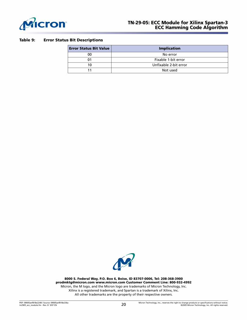
Table 9: Error Status Bit Descriptions
Error Status Bit Value Implication
00 No error01 Fixable 1-bit error10 Unfixable 2-bit error11 Not used
®
8000 S. Federal Way, P.O. Box 6, Boise, ID 83707-0006, Tel: [email protected] www.micron.com Customer Comment Line: 800-932-4992
Micron, the M logo, and the Micron logo are trademarks of Micron Technology, Inc. Xilinx is a registered trademark, and Spartan is a trademark of Xilinx, Inc.
All other trademarks are the property of their respective owners.
PDF: 09005aef818e2248 / Source: 09005aef818e236a Micron Technology, Inc., reserves the right to change products or specifications without notice.tn2905_ecc_module.fm - Rev. B 5/07 EN 20 ©2005 Micron Technology, Inc. All rights reserved.
TN-29-05: ECC Module for Xilinx Spartan-3Revision History
Revision History
Rev. B . . . . . . . . . . . . . . . . . . . . . . . . . . . . . . . . . . . . . . . . . . . . . . . . . . . . . . . . . . . . . . . . . . . . . . . . . . . . . . . . . . . . . . . . . . . . . . . 5/07• Updated Web links.• “Overview” on page 1: Revised description.• “Micron ECC Module Configuration” on page 2: Revised description.• “Interface and Timing Specifications” on page 6: Revised description.• “ECC Finite Control Logic Module” on page 10: Revised description.• “Write States” on page 12: Revised description.• Table 5 on page 13: Changed “state machine” to “control logic.”• Table 6 on page 17: Revised ECC error description, consolidated notes 1 and 2.
Rev. A . . . . . . . . . . . . . . . . . . . . . . . . . . . . . . . . . . . . . . . . . . . . . . . . . . . . . . . . . . . . . . . . . . . . . . . . . . . . . . . . . . . . . . . . . . . . . . . 4/05• Initial release.
PDF: 09005aef818e2248 / Source: 09005aef818e236a Micron Technology, Inc., reserves the right to change products or specifications without notice.tn2905_ecc_module.fm - Rev. B 5/07 EN 21 ©2005 Micron Technology, Inc. All rights reserved.