Embed Size (px)
Citation preview
Stanford University
Let’s Start with the MOS Capacitor
Silicon dioxide
Gate electrode(metal or polysilicon)
tox
Silicon substrate
Department of Electrical EngineeringH.-S. Philip Wong EE 3162-8
Stanford University
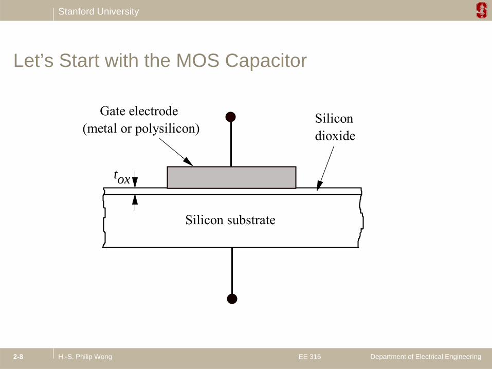
Metal-Oxide-Semiconductor (MOS)Silicon dioxide
Gate electrode(metal or polysilicon)
tox
( )
Vacuum Vacuum
Silicon substrate
Vacuum level
Vacuum level
Ec
= 4.10 eV
0.95 eV
= 4.05 eVqq mq s
High-k:
Eg and barrier h i ht diff t
Ec
Ev
8-9 eV
q s
Metal(aluminum)
1.12 eV
Eg q B
EiEf
Ef
height are different from SiO2
Alternative channel
Ev
v(aluminum) Silicon(p-type)
Alternative channel materials:
Eg, barrier height, and dielectric constant are different from SigE
Department of Electrical EngineeringH.-S. Philip Wong EE 3162-9
Silicondioxide
are different from Si sg
Bq
2
Stanford University
p-type n-type
Accumulation, Depletion, Inversion
(a) (e)Ec
EEfEf
V = 0g
Ec
Ev
Ef
Ef
V = 0g
p type n-type
flatband
+ + + + + +
_ _ _ __ __ _Assume m=s:Ev
Ev
accumulationV < 0
+ + + + + + + +
(b) (f)Ec
Ev
Ef
Ef
Ec
Ev
Ef Ef
accumulationV < 0g V > 0g
+ + + + + +
_ __ __
+ +
_ _ __ ______ __
+++
+ ++ ++
(c) (g)depletion
Ec
Ev
Ef Ef
V > 0g
Ec
Ev
Ef
Ef
V < 0g
+ + + + +
_ _ _ __ __
+ +
(d) (h)inversion
Ec EcE
Ef
V < 0g
__ ___ ____ __ ___ ____
Department of Electrical EngineeringH.-S. Philip Wong EE 3162-10
( ) ( )c
Ev
Ef
Ef
V > 0g Ev
Ef
+ + + + + +
_
++ +++++ +++
+
Stanford University
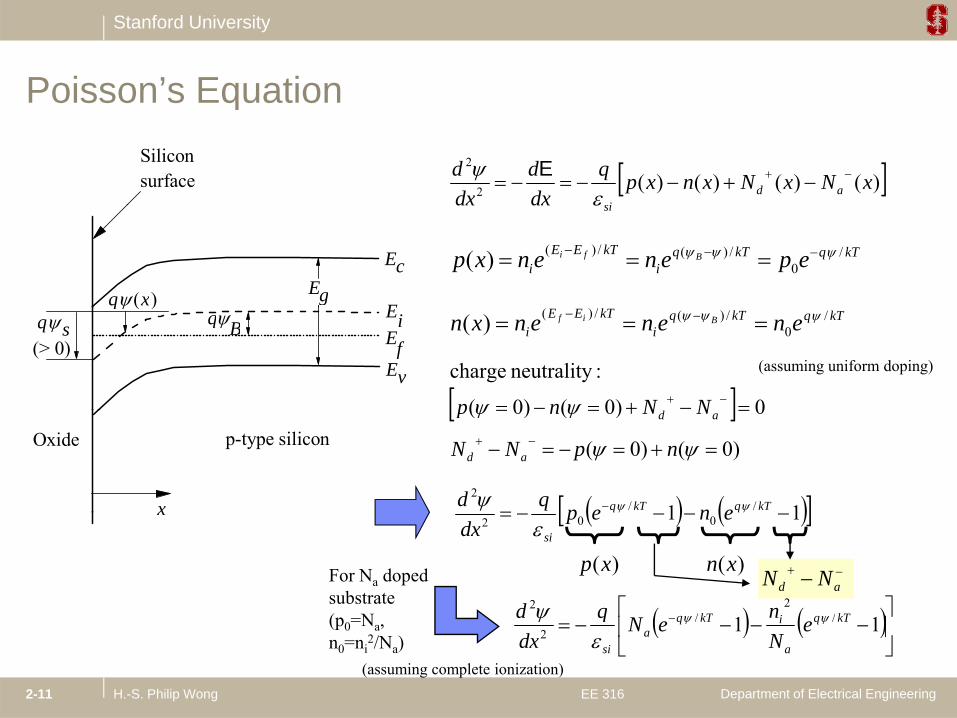
Poisson’s EquationSiliconsurface )()()()(2
2
xNxNxnxpqdxd
dxd
adi
E
Poisson s Equation
Ec
EEgq x ( )
dxdx si
kTqkTqi
kTEEi epenenxp Bfi /
0/)(/)()(
q s(> 0)
Ei
Ev
q Bq ( )
Ef
kTqkTqi
kTEEi enenenxn Bif /
0/)(/)()(
(assuming uniform doping)
0)0()0(
:neutralitycharge
NNnp Oxide p-type silicon
x
0)0()0( ad NNnp
)0()0( npNN ad
11 //2
kTqkTq enepqd x
/2
/2
kTkT nqd
For Na doped substrate ( N
)(xp )(xn ad NN
11 002 si
enepdx
Department of Electrical EngineeringH.-S. Philip Wong EE 3162-11
11 //
2kTq
a
ikTqa
si
eNneNq
dxd
(p0=Na,
n0=ni2/Na)
(assuming complete ionization)
Stanford University
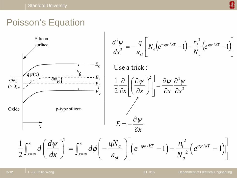
Poisson’s EquationSiliconsurface
Poisson s Equation
11 /
2/
2
2kTqikTq
a eNneNq
dd
Ec
EEgq x ( )
2asi Ndx
2
:trickaUse
q s(> 0)
Ei
Ev
q Bq ( )
Ef
2
22
21
xxxx
Oxide p-type silicon
x E
x x
2 2
/ /2
1 1 12
x x q kT q kTa iqN ndd d e ed N
Department of Electrical EngineeringH.-S. Philip Wong EE 3162-12
22 x xsi adx N
Stanford University
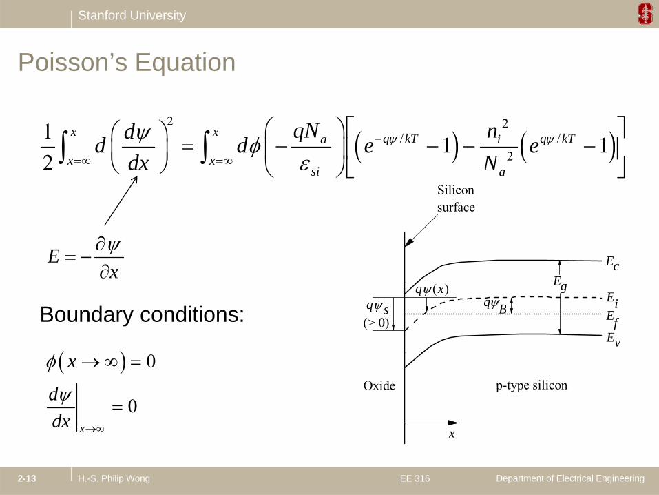
Poisson’s EquationPoisson s Equation
2 2
/ /1 1 1x x q kT q kTa iqN ndd d
/ /2 1 1
2q kT q kTa i
x xsi a
qd d e e
dx N
Siliconsurface
Ex
EcE
Boundary conditions: q s(> 0)
Ei
Ev
Egq B
q x ( )
Ef
Oxide p-type silicon
0
0
x
ddx
Department of Electrical EngineeringH.-S. Philip Wong EE 3162-13
xxdx
Stanford University
2
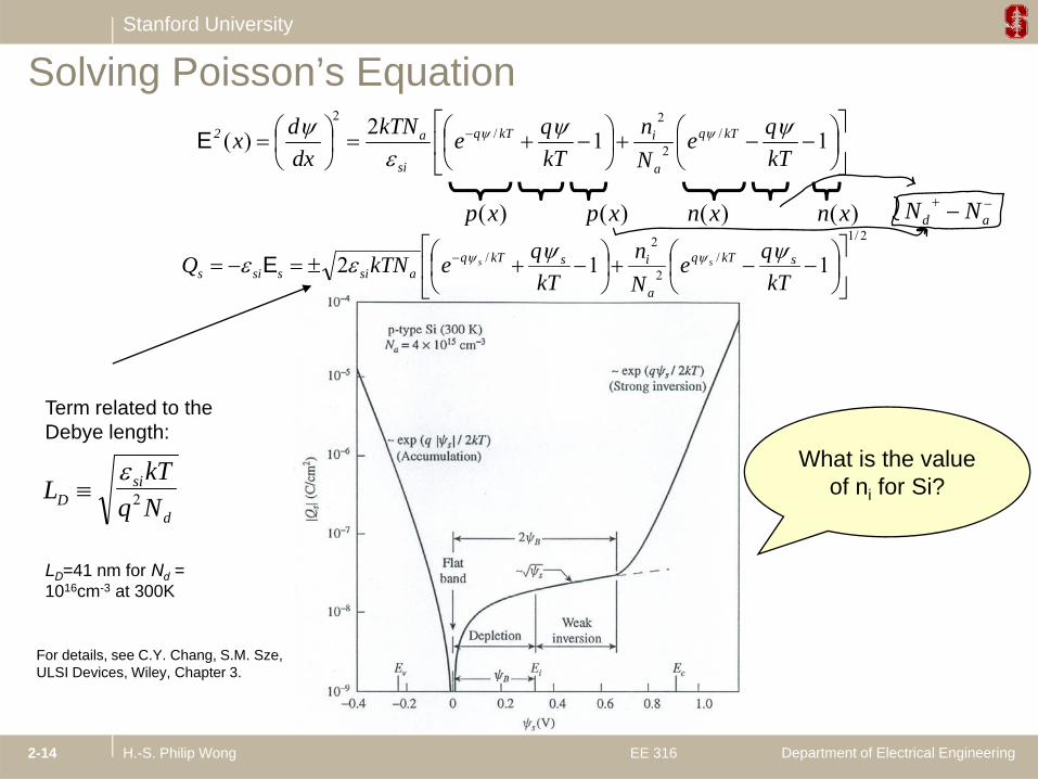
Solving Poisson’s Equation
112)( /
2
2/
2
kTqe
Nn
kTqekTN
dxdx kTq
a
ikTq
si
a2
E
)(xp )(xn)(xp )(xn ad NN2/1
/2
2/ 112
kTqe
Nn
kTqekTNQ skTq
a
iskTqasissis
ss E
)(p )()(p )( ad
Term related to the Debye length:
LkT
q NDsi
d
2
What is the value of ni for Si?
For details, see C.Y. Chang, S.M. Sze, ULSI D i Wil Ch t 3
LD=41 nm for Nd = 1016cm-3 at 300K
Department of Electrical EngineeringH.-S. Philip Wong EE 3162-14
ULSI Devices, Wiley, Chapter 3.
Stanford University
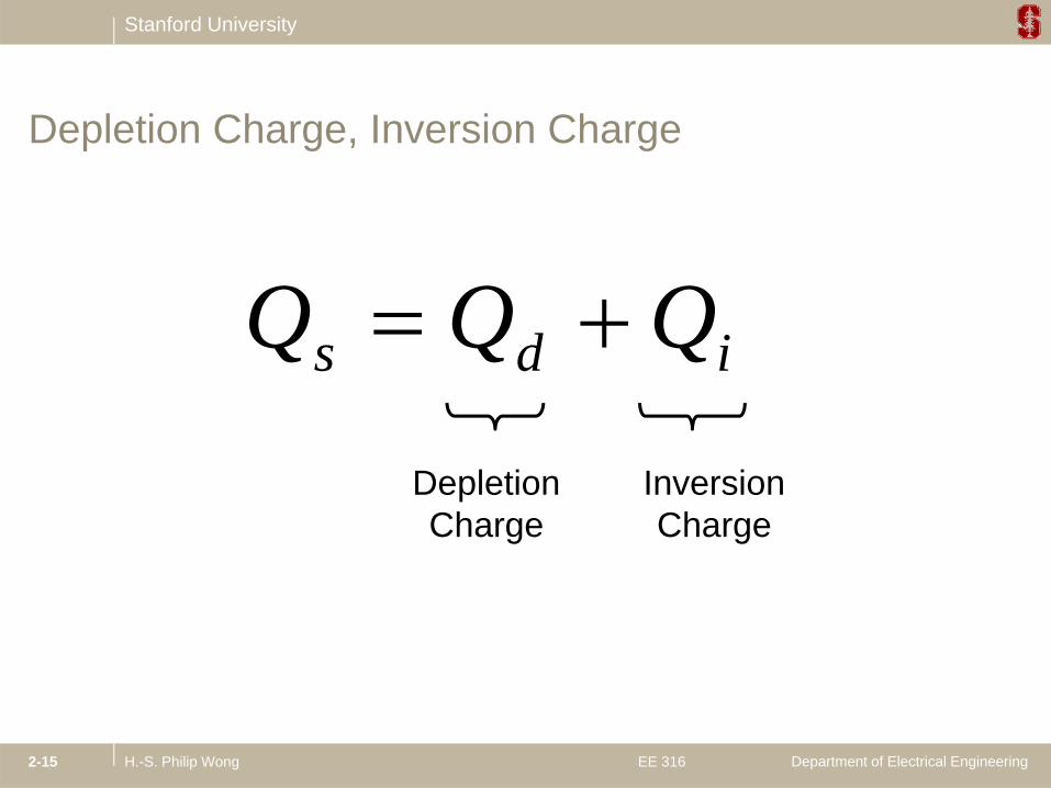
Depletion Charge, Inversion Charge
id QQQ ids QQQ Depletion Charge
Inversion Charge
Department of Electrical EngineeringH.-S. Philip Wong EE 3162-15
Stanford University
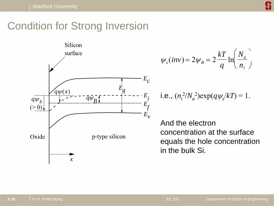
Condition for Strong InversionSiliconsurface
ainvkT N
( ) ln
2 2
Condition for Strong Inversion
EcE
s Bi
invq n
( ) ln
2 2
q s(> 0)
Ei
Ev
Egq B
q x ( )
Ef
i.e., (ni2/Na
2)exp(qs/kT) = 1.
v
Oxide p-type silicon
And the electron concentration at the surface equals the hole concentration
xin the bulk Si.
Department of Electrical EngineeringH.-S. Philip Wong EE 3162-16
Stanford University
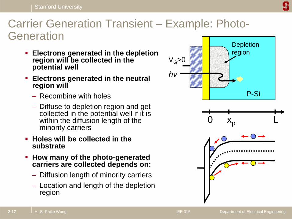
Carrier Generation Transient – Example: Photo-Generation
Electrons generated in the depletion region will be collected in the VG>0
Depletion region
eg o be co ected t epotential well
Electrons generated in the neutral region will
R bi ith h l P Si
G
hν
– Recombine with holes– Diffuse to depletion region and get
collected in the potential well if it is within the diffusion length of the
i it i
P-Si
0 xp Lminority carriers
Holes will be collected in the substrate
How many of the photo generated
p
How many of the photo-generated carriers are collected depends on:– Diffusion length of minority carriers– Location and length of the depletion
Department of Electrical EngineeringH.-S. Philip Wong EE 3162-17
Location and length of the depletion region
Stanford University
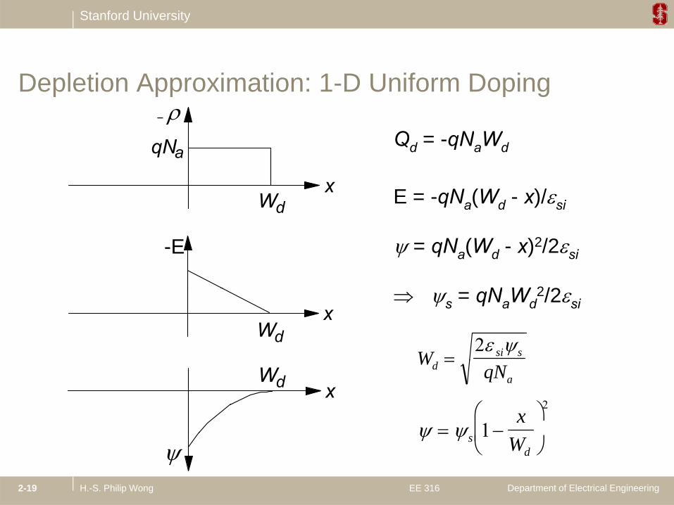
qN
Qd = -qN Wd
Depletion Approximation: 1-D Uniform Doping
Wdx
qNaQd qNaWd
E = -qNa(Wd - x)/si
E-E = qNa(Wd - x)2/2si
N W 2/2x
Wd
s = qNaWd2/2si
W si s2
xWd
WqNd
a
x1
2
Department of Electrical EngineeringH.-S. Philip Wong EE 3162-19
s
dW1
Stanford University
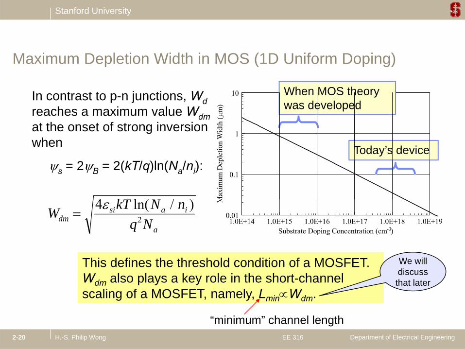
In contrast to p-n junctions, Wd10
Maximum Depletion Width in MOS (1D Uniform Doping)
When MOS theory In contrast to p n junctions, Wdreaches a maximum value Wdmat the onset of strong inversion when
1
ion
Wid
th (µ
m)
Today’s device
was developed
k4 l ( / )
s = 2B = 2(kT/q)ln(Na/ni): 0.1
Max
imum
Dep
leti Today s device
W kT N nq Ndm
si a i
a
4
2 ln( / )
1.0E+14 1.0E+15 1.0E+16 1.0E+17 1.0E+18 1.0E+190.01
Substrate Doping Concentration (cm )M
-3
This defines the threshold condition of a MOSFET.Wdm also plays a key role in the short-channel scaling of a MOSFET, namely, LminWdm.
We will discuss that later
Department of Electrical EngineeringH.-S. Philip Wong EE 3162-20
g , y, min dm
“minimum” channel length
Stanford University
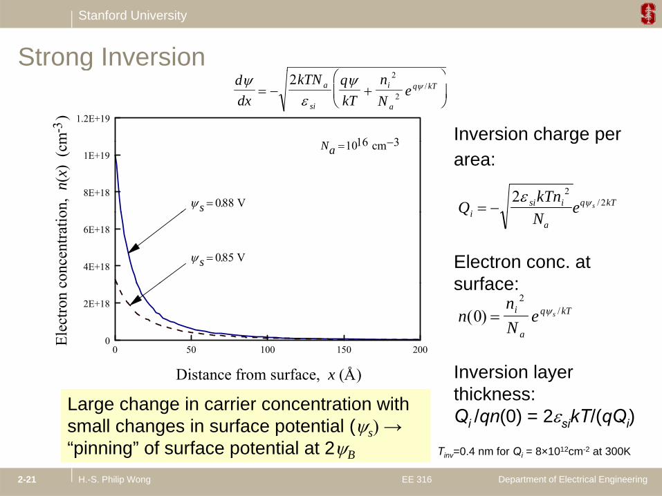
Strong Inversion
ddx
kTN qkT
nN
ea
si
i
a
q kT
2 2
2/
1.2E+19
N 1016 3m
)-3 Inversion charge per
g
8E+18
1E+19Na 1016 3cm
s 088. V
on,
n(x)
(cm
g parea:
QkTn
eisi i q kTs
2 22 /
4E+18
6E+18
s 085. V
conc
entra
tio
Electron conc. at surface:
QN
eia
0 50 100 150 2000
2E+18
Elec
tron
c surface:
nnN
ei
a
q kTs( ) /02
Distance from surface, x ( )Å Inversion layer thickness: Qi /qn(0) = 2sikT/(qQi)
Large change in carrier concentration with small changes in surface potential ( ) →
Department of Electrical EngineeringH.-S. Philip Wong EE 3162-21
i q ( ) si (q i)small changes in surface potential (s) →“pinning” of surface potential at 2B Tinv=0.4 nm for Qi = 8×1012cm-2 at 300K
Stanford University
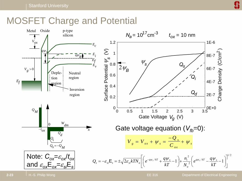
MOSFET Charge and Potential
1.2 1E-6
V) )
t = 10 nmoxN = 10 cma17 -3
2
Oxide p-type silicon
q s
Ec
Metal
Vox
g
0.6
0.8
1
6E-7
8E-7
oten
tial
(
V
nsity
(C
/cm
s s
2
Qs
Qi
B
q sEi
Ev
q B
Vg 0Deple-tion
Neutral region
Ef
0.2
0.4
2E-7
4E-7
Surfa
ce P
o
Cha
rge
Den
Qd
Qitionregion
Inversionregion
regionEf
0 0.5 1 1.5 2 2.5 3 3.50 0E+0
Gate Voltage (V)Vg
QM
0xt
Wdm Gate voltage equation (Vfb=0):Qd
QiQs QM
xtox Gate voltage equation (Vfb 0):
V VQ
Cg o x ss
o xs
Note C /t 2/1
Department of Electrical EngineeringH.-S. Philip Wong EE 3162-23
Note: Cox=ox/toxand oxEox=siEs
2/1
/2
2/ 112
kTqe
Nn
kTqekTNQ skTq
a
iskTqasissis
ss E
Stanford University
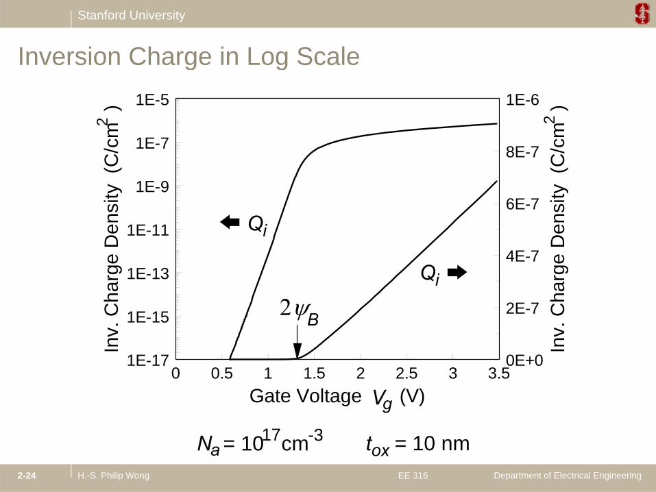
Inversion Charge in Log Scale
1E 7
1E-5 1E-6cm
)
cm )22
g g
1E-9
1E-7
6E-7
8E-7
sity
(C
/c
sity
(C
/c
1E-13
1E-114E-7
rge
Den
s
rge
Den
s
Qi
Qi
1E-15 2E-7
Inv.
Cha
Inv.
Cha
Qi
B
0 0.5 1 1.5 2 2.5 3 3.51E-17 0E+0
Gate Voltage (V)Vg
Department of Electrical EngineeringH.-S. Philip Wong EE 3162-24
t = 10 nmoxN = 10 cma17 -3
Stanford University
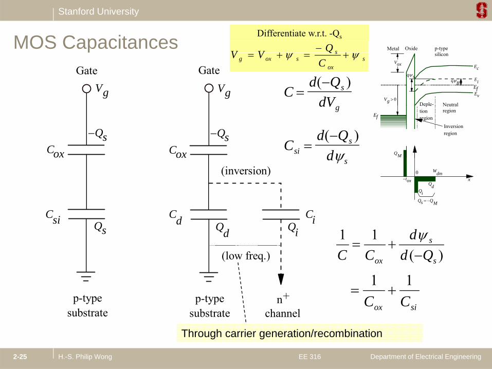
MOS Capacitances Oxide p-type ili
Metal
Differentiate w.r.t. -Qs
sQVV
GateGate
Vg Vg Cd Q
dVs
( )
silicon
q s
Ec
Ei
Ev
q B
Vg 0
Vox
Deple- Neutral
Ef
sox
ssoxg C
QVV
CoxCox
Qs Qs
dVg
Cd Q
dsis
( ) QM
Depletionregion
Inversionregion
Neutral region
Ef
C C
(inversion)
C
d s
QdQi
0
Qs QM
xtox
Wdm
Csi Ci
(low freq.)
CdQs Qd Qi
)(11
s
s
ox Qdd
CC
p-typesubstrate
n+channel
p-typesubstrate
sox
siox CC11
Department of Electrical EngineeringH.-S. Philip Wong EE 3162-25
substrate channelsubstrate
Through carrier generation/recombination
Stanford University
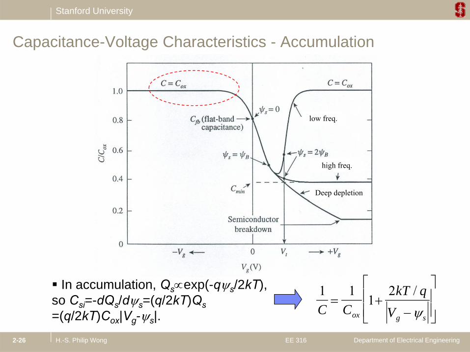
Capacitance-Voltage Characteristics - Accumulationg
low freq.
high freq.
Deep depletion
In accumulation, Qsexp(-qs/2kT), so C i=-dQ /d =(q/2kT)Q
1 11
2kT q
/
Department of Electrical EngineeringH.-S. Philip Wong EE 3162-26
so Csi=-dQs/ds=(q/2kT)Qs=(q/2kT)Cox|Vg-s|.
1C C Vox g s
Stanford University
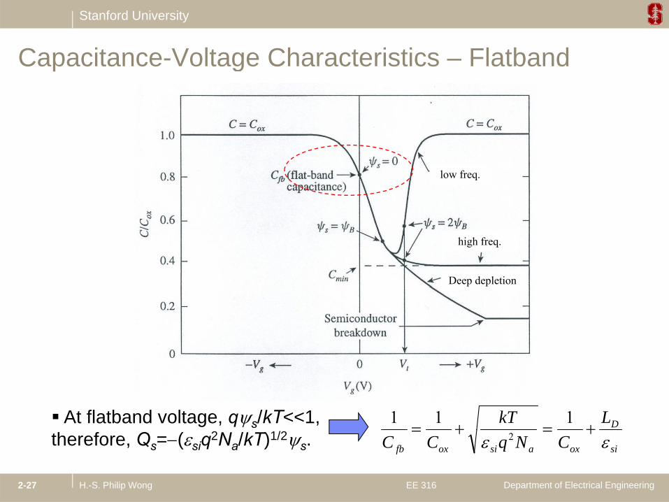
Capacitance-Voltage Characteristics – Flatbandg
low freq.
high freq.
Deep depletion
At flatband voltage, qs/kT<<1, DLkT
111
Department of Electrical EngineeringH.-S. Philip Wong EE 3162-27
therefore, Qs=(siq2Na/kT)1/2s. sioxasioxfb CNqCC 2
Stanford University
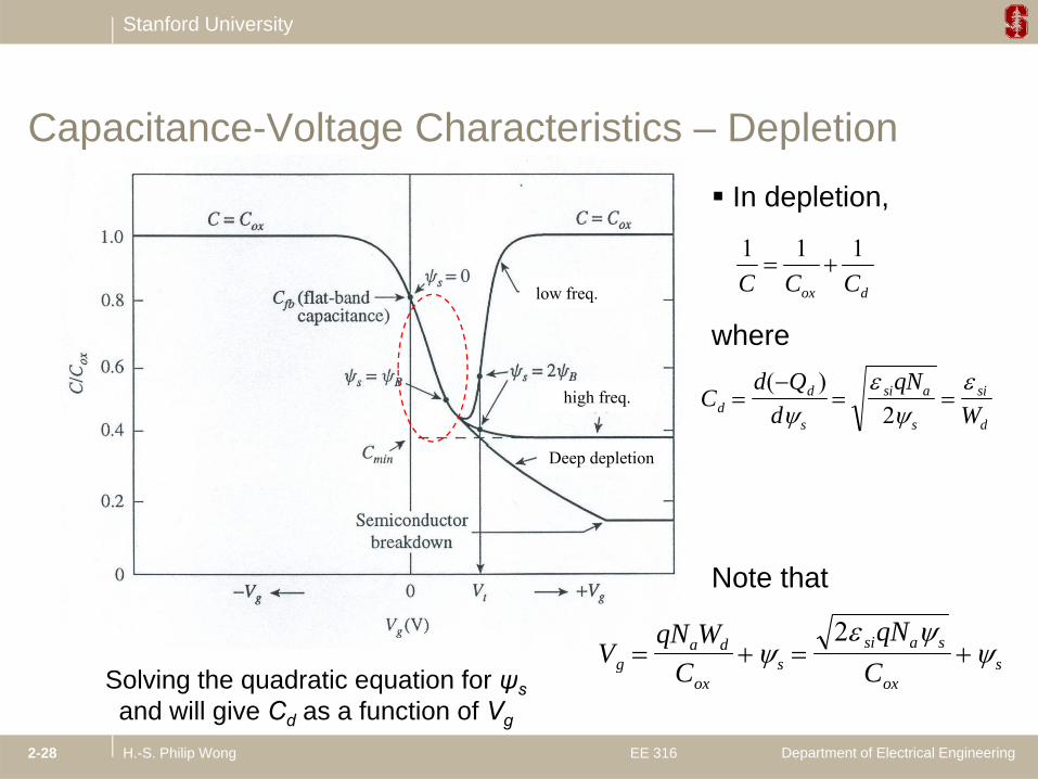
In depletion,
Capacitance-Voltage Characteristics – Depletion
wheredox CCC
111 low freq.
where
Cd Q
dqN
Wdd
s
si a
s
si
d
( )
2
high freq.
Deep depletion
Note that
VqN W
CqN
Cga d
ssi a s
s
2
Department of Electrical EngineeringH.-S. Philip Wong EE 3162-28
C Cgox
sox
s Solving the quadratic equation for ψsand will give Cd as a function of Vg
Stanford University
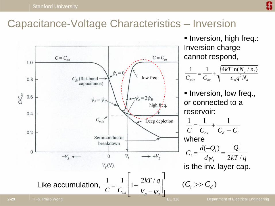
Capacitance-Voltage Characteristics – Inversion Inversion, high freq.:Inversion charge cannot respond,
g
cannot respond,
1 1 4
2C CkT N n
q Nox
a i
si amin
ln( / )
low freq.
Inversion, low freq., or connected to a reservoir:
high freq.
where
1 1 1C C C Cox d i
d Q Q( )
Deep depletion
is the inv. layer cap.
Cd Q
dQ
kT qii
s
i
( )
/ 2
Department of Electrical EngineeringH.-S. Philip Wong EE 3162-29
1 1
12
C CkT q
Vox g s
/
Like accumulation, )( di CC
Stanford University
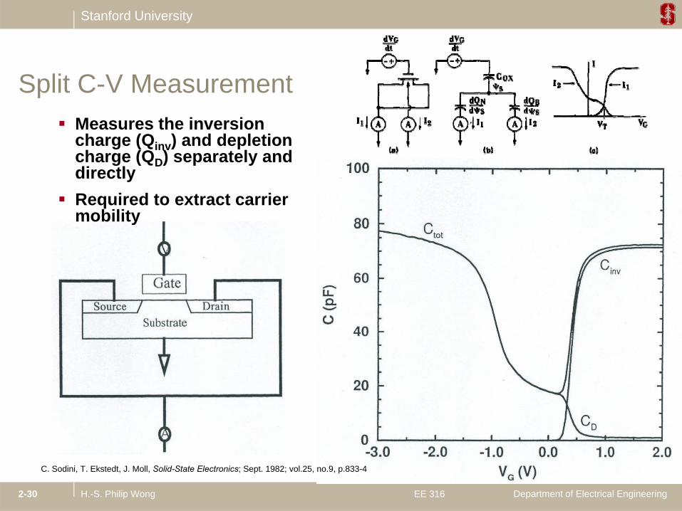
Split C-V Measurement Measures the inversion
charge (Qinv) and depletion c a ge (Qinv) a d dep et ocharge (QD) separately and directly
Required to extract carrier mobilitymobility
Department of Electrical EngineeringH.-S. Philip Wong EE 3162-30
C. Sodini, T. Ekstedt, J. Moll, Solid-State Electronics; Sept. 1982; vol.25, no.9, p.833-4
Stanford University
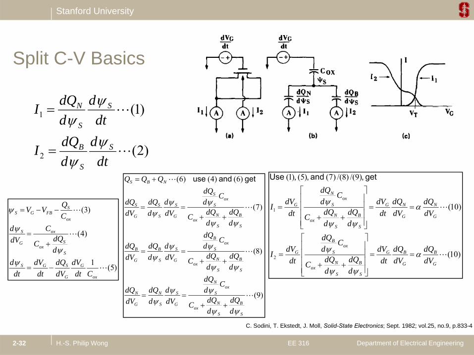
Split C-V Basics
ddQ
)2(
)1(1
ddQI
dtd
ddQI
SB
S
S
N
)2(2 dtdI
S
Q
)6()4()6(
oxS
NBS
CddQ
ddQdQ
QQQ
getanduse )9/()8/()7()5()1(
oxN
dQdQdVC
ddQ
dV
get,and , , Use
)4(
)3(
S
Sox
ox
G
S
ox
SFBGS
ddQC
CdVd
CQVV
)8(
)7(
oxS
B
SBB
S
B
S
Nox
S
G
S
S
S
G
S
dQdQ
CddQ
ddQdQ
ddQ
ddQC
ddVd
ddQ
dVdQ
)10(
)10(1
BBGox
S
B
G
G
N
G
NG
S
B
S
Nox
SG
dQdQdVC
ddQ
dVI
dVdQ
dVdQ
dtdV
ddQ
ddQC
ddt
dVI
)5(1 ox
G
G
SGS
S
CdtdV
dVdQ
dtdV
dtd
)9(
)8(
BN
oxS
N
G
S
S
N
G
N
S
B
S
Nox
GSG
dQdQC
CddQ
dVd
ddQ
dVdQ
ddQ
ddQCdVddV
)10(2
G
B
G
BG
S
B
S
Nox
SG
dVdVdtddQ
ddQCdt
I
Department of Electrical EngineeringH.-S. Philip Wong EE 3162-32
S
B
S
Nox
GSG
dQ
dQC
C. Sodini, T. Ekstedt, J. Moll, Solid-State Electronics; Sept. 1982; vol.25, no.9, p.833-4
Stanford University
C-V Measurement
When performing CV meas rements start from When performing CV measurements, start from inversion and sweep the gate voltage to accumulation
Inversion layer build up is a slower process than collapsing the inversion layer and forming the
l ti l ( T & Ni 28accumulation layer (see Taur & Ning p. 28, Chapter 2.1.4.6)
Department of Electrical EngineeringH.-S. Philip Wong EE 3162-33
Stanford University
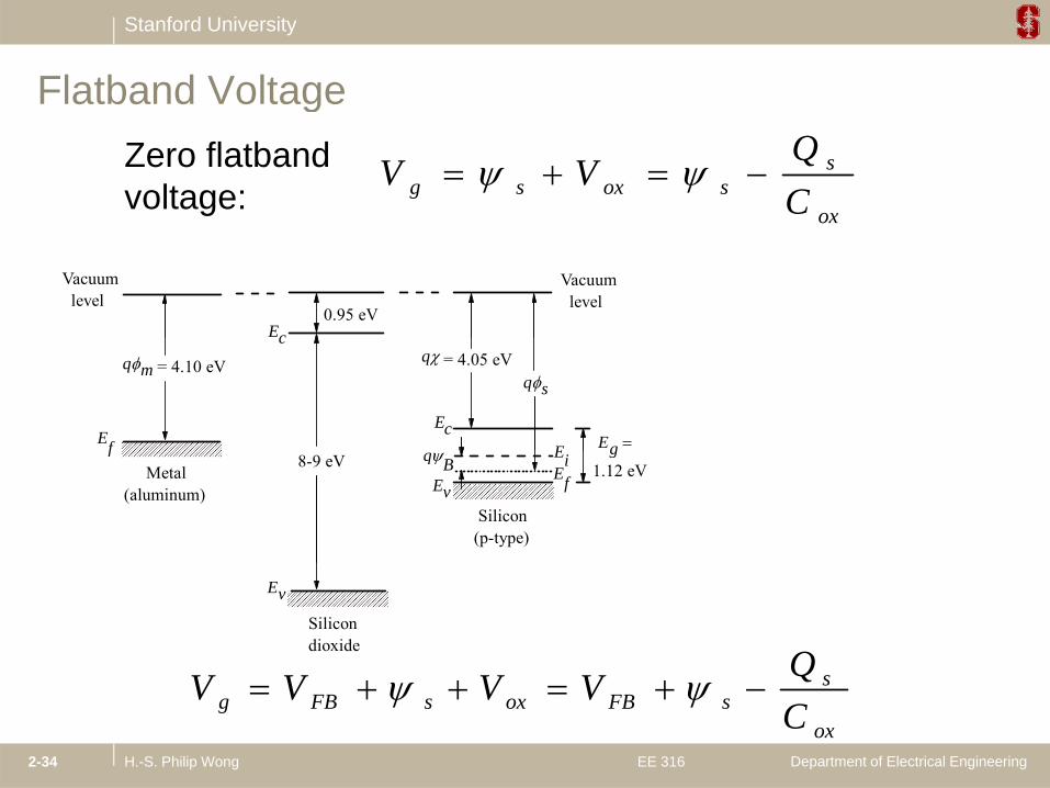
Flatband Voltageg
ox
ssoxsg C
QVV Zero flatband
voltage:
Vacuum level
Vacuum level
Ec0.95 eV
c
Ec
= 4.10 eV = 4.05 eVqq mq s
Eg EEf
Ev
8-9 eV Metal(aluminum)
Silicon(p-type)
1.12 eVgq B
EiEf
f
Ev
Silicondioxide
QVVVV
Department of Electrical EngineeringH.-S. Philip Wong EE 3162-34
ox
ssFBoxsFBg C
QVVVV
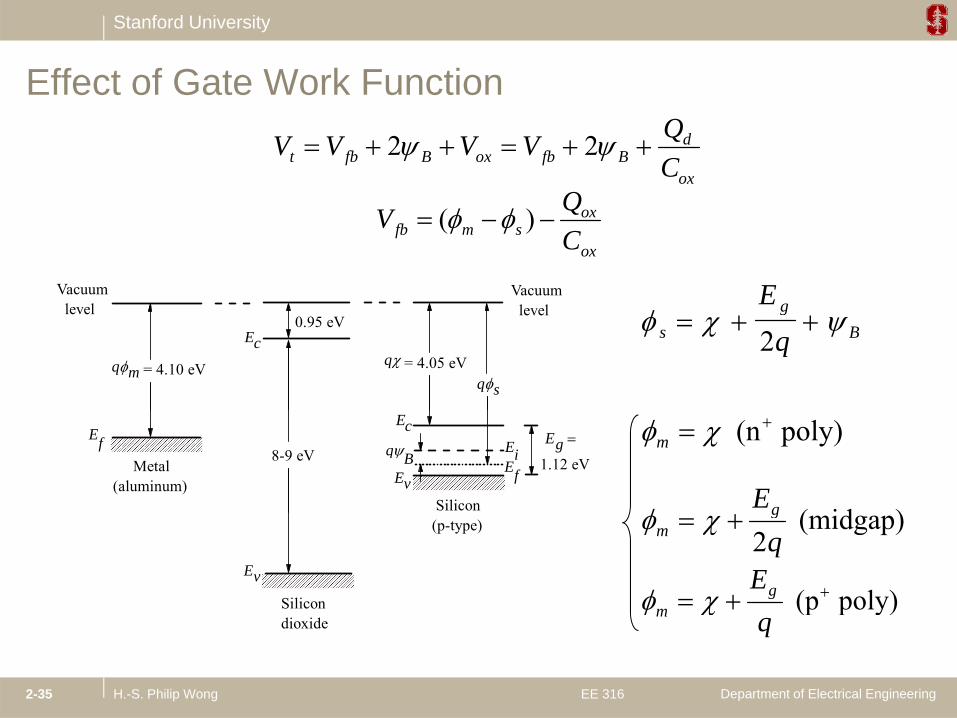
Stanford University
Effect of Gate Work Function V V V V Q
Ct fb B ox fb Bd
ox
2 2
Q
Vacuumlevel
Vacuuml l
ox
oxsmfb C
QV )(
gE level level
Ec
= 4.10 eV
0.95 eV
= 4.05 eVqq mq s
sg
Bq
2
Ec
Ev
8-9 eV Metal(aluminum)
Silicon
1.12 eV
Eg q B
EiEf
Ef
poly) (n m
( id )Eg
Ev
Silicon
(p-type)
poly)(p Eg
m
(midgap) 2q
gm
Department of Electrical EngineeringH.-S. Philip Wong EE 3162-35
dioxidep y)(p
qm
Stanford University
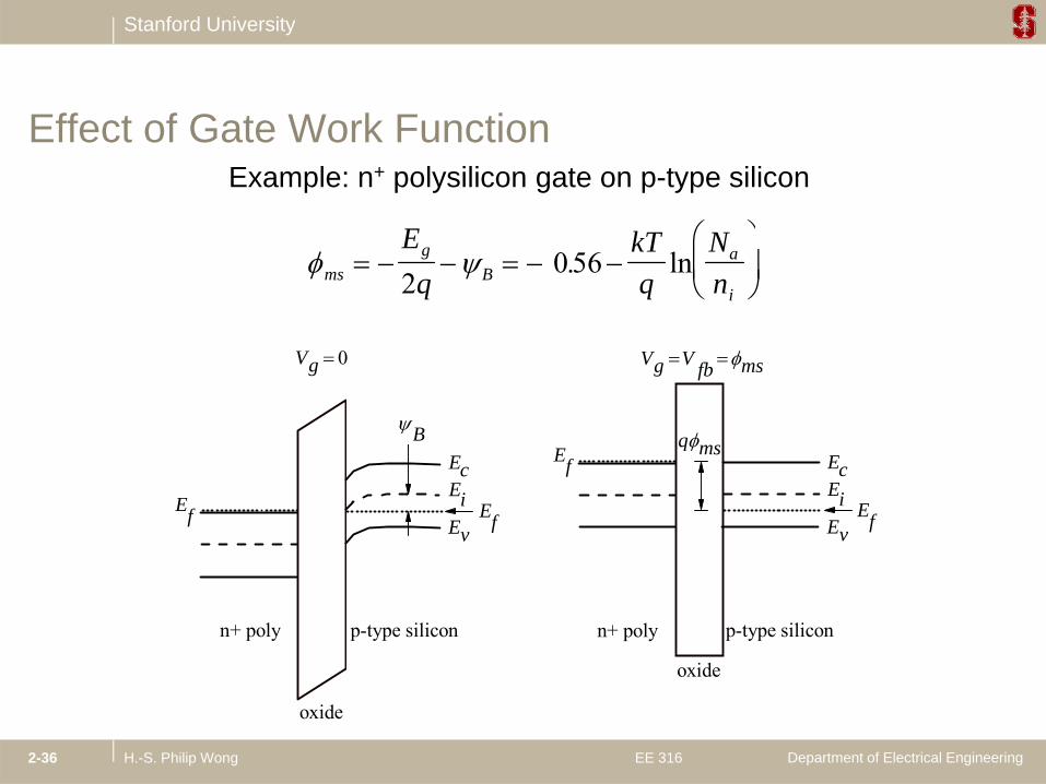
Example: n+ polysilicon gate on p-type silicon
Effect of Gate Work Function
msg
Ba
i
Eq
kTq
Nn
2
0 56. ln
q ms
Vg V fb ms Vg 0
B q msEc
Ev
Ei
Ec
Ev
EiEf
Ef
Ef Ef
oxide
p-type siliconn+ polyn+ poly p-type silicon
Department of Electrical EngineeringH.-S. Philip Wong EE 3162-36
oxide
oxide
Stanford University
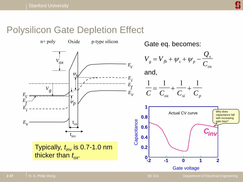
p-type siliconOxiden+ poly
QGate eq. becomes:
Polysilicon Gate Depletion Effect
Ec
E
Vox
s
V VQCg fb s p
s
ox
and,Ei
EvEcVg
p
Ef
Ef
1 1 1 1C C C Cox si p
Ei
Ev
pf
0.6
0.8
1
C
Actual CV curve Why does capacitance fall with increasing gate bias?
tanc
etox
Typically, tinv is 0.7-1.0 nm thicker than t 0
0.2
0.4Cinv
Cap
acit
tinv
Department of Electrical EngineeringH.-S. Philip Wong EE 3162-37
thicker than tox. -2 -1 0 1 20
Gate voltage


![EKG Basics.ppt [Read-Only]](https://img.pdfslide.net/doc/110x75/615cd04d66f1ad2531041f36/ekg-read-only.jpg)