Embed Size (px)
Citation preview
Operations manual 1
SPD operations manual
for users and experts
SPD
15 June 2008 last update: 27/2/2017
SPD Operations manual 2
Content
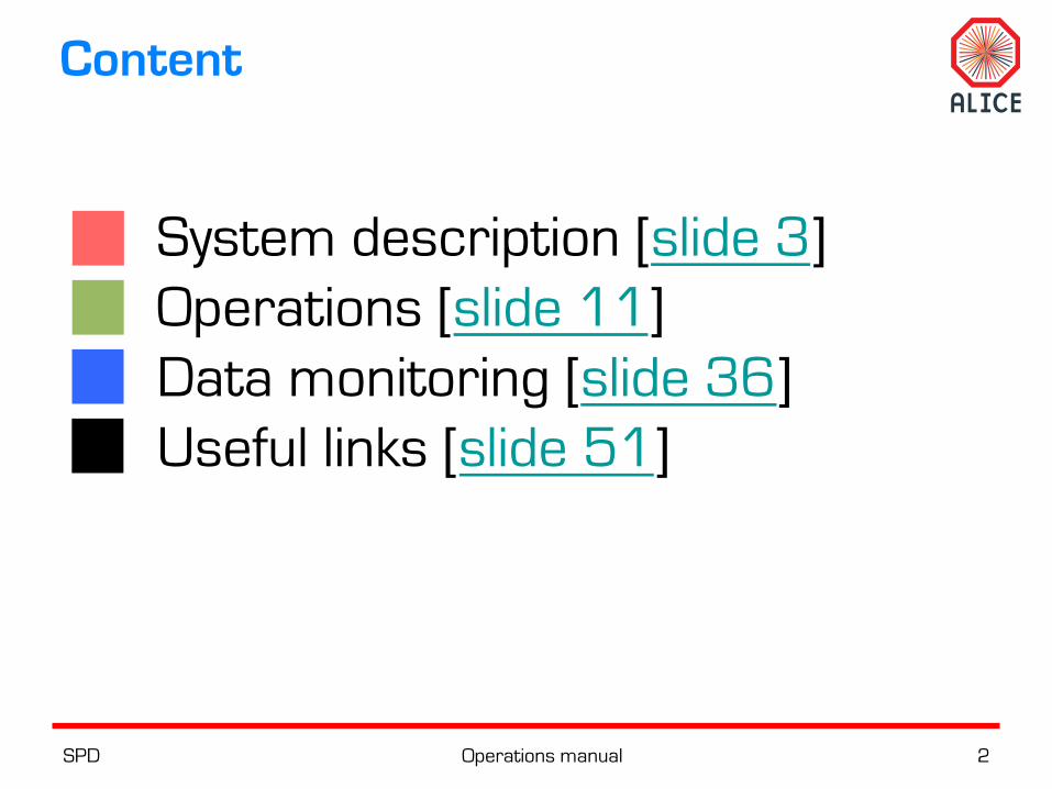
System description [slide 3] Operations [slide 11] Data monitoring [slide 36] Useful links [slide 51]
SPD Operations manual 3
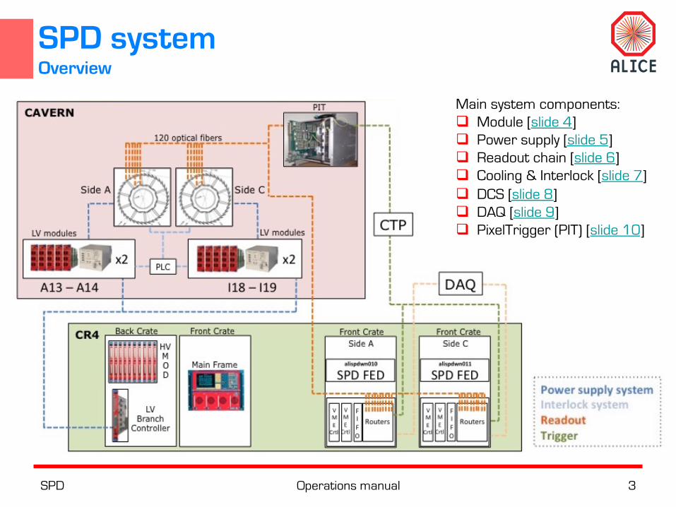
SPD system Overview
Main system components: q Module [slide 4] q Power supply [slide 5] q Readout chain [slide 6] q Cooling & Interlock [slide 7] q DCS [slide 8] q DAQ [slide 9] q PixelTrigger (PIT) [slide 10]
SPD Operations manual 4
SPD system Module
1) ANALOG_GND [25 µm] 2) ANALOG_POWER [25 µm] 3) HORIZONTAL LINES [10 µm] 4) VERTICAL LINES [5 µm] 5) DIGITAL POWER [25 µm] 6) DIGITAL_GND [25 µm]
0
1
23
4
5
The Silicon Pixel Detector (SPD) consist of two barrel layers of silicon pixel detectors located at an average distance of 39 mm and 76 mm from the beam line (the first two layers of ITS). Ten Sectors are mounted around the beam pipe to form the full barrel. The detector is divided in two independent side (A and C).
The basic detector module, the HALF STAVE, consists of two silicon ladders, one Multi-Chip Module (MCM) and one high density aluminium/polyimide multi-layer interconnect. The ladder consists of a silicon sensor matrix bump bonded to 5 the ALICE1LHCb read-out chips. The sensor matrix includes 256 × 160 cells measuring 50 μm (rφ) by 425 μm (z), having a sensitive area of 12.8 mm (rφ) x 69.6 mm (z). The thickness of the sensor is 200 μm. In total, there are 120 half staves, 240 ladders, 1200 chips and 9.8×10⁶ cells.
The readout and control chips are wire-bonded to a multilayer carrier bus for data, controls and power distribution. The bus for each half-stave has six aluminium layers on polyamide support. Electrical power is supplied to the front-end electronics using a copper multilayer flex. The readout chip control and parameter downloading is done using the JTAG protocol.
SPD Operations manual 5
SPD system Power supply
The module SY1527 is the primary system of the high and low voltage power supplying system. It consist of four parts: the “Board Section” (with 16 slots to house boards, distributors and branch controllers), the “Fan Tray Section”, the “Power Supply Section” and the “CPU and Front Panel Section” which includes all interface facilities. The system allows to deal with power supply solutions composed by “branch controllers” (housed in the system main frame) and on-detector “remote boards” (manufactured in order to be magnetic field and radiation tolerant). This is the solution adopted for the Low voltage. A module A1676A EASY Branch Controller, housed in the board section of the mainframe, is linked to four EASY3000 crate (placed in the cavern) via two front panel connectors (control and power supply) and is the interface between the mainframe and the remote boards. The channels of the EASY3000 boards operate as channels of the A1676A.
The low-voltage power supply system is based on 20 CAEN A3009 dc-dc converter modules housed in 4 CAEN Easy3000 crates located in the experimental area (cavern) at a distance of ≈ 40 m from the detector (two racks, one for each side). Each half-sector (6 half-staves) is powered by one module, which has 12 independent floating outputs; 2 outputs are used for each half-stave, one for the pixel chips (1.85V/5.5A), the other one for the MCM (2.6V/0.5A). The detector bias voltage (50 V typically at start of detector operation) is provided by CAEN A1519 modules located in the control room (CR4 - behind the mainframe) at a distance of ≈ 120 m from the detector. One module (12 channels) is used for each sector.
SPD Operations manual
SPD system Readout chain
ROUTER
LRx
DDL
TTC
LDCs(DAQ)
CTP
SEMISECTOR
6HALFSTAVES
-
DCSECS
FEDs
LRx
LRx
USB
SerialGlinkClock
Ethernet
SerialGlinkClock
ON--DETECTOR § The chip clock frequency is 10 MHz. § Each pixel cell contains a preamplifier-shaper with leakage current compensation, followed by a
discriminator. A signal above threshold results in a logical 1 which is propagated through a delay line during the L1 trigger latency (≈ 6 μs). A four-hit-deep multi-event buffer in each cell allows de-randomization of the event arrival times. Upon arrival of the L1 trigger, the logical level present at the end of the delay line is stored in the first available buffer location.
§ Upon arrival of the second level trigger (L2), the data contained in the multi-event buffer locations are loaded onto the output shift registers. Then, for each chip, the data from the 256 rows of cells are shifted out during 256 cycles of a 10 MHz clock. At each cycle, a 32-bit word containing the hit pattern from one chip row is output on the 32-bit data bus where it is processed by the MCM and sent optically to the read-out electronics located in the counting room.
§ One pixel chip is read out in 25.6 μs. § The 10 chips on each half-stave are read out sequentially. § The 120 half-staves are read out in parallel.
Cavern
OFF--DETECTOR § The SPD off-detector read-out electronics is located in the CR4. Twenty 9U VME- and FPGA-based
electronics cards (routers) contain each 3 plug-in type daughter cards (link receiver cards, LRX). § Each LRX is connected via optical fibers to two half-staves. The LRx zero-suppress and re-format the
hit data to an ALICE off-line analysis compatible format. The routers multiplex data from the six half-staves into one ALICE optical Detector Data Link (DDL) and attach trigger and status information.
§ For each of the 20 router cards: 1) the trigger information is delivered by the Trigger, Timing and Control (TTC) system via optical
fibers; 2) each router is interfaced to the DAQ via one DDL and the 20 DDLs are connected to Local
Data Collectors (LDCs) housed in 7 PCs; 3) the data access from the DCS/ECS to the routers is established via the router VME ports; the
same port also allows monitoring and copying the data flow during data taking.
CR4
6
SPD Operations manual 7
SPD system Cooling & Interlock
The major contribution to the on-detector power dissipation is due to front-end chips that generate a heat load of ≈ 23 W (nominal) in each stave. The final choice of an evaporative system with C4F10 as coolant was found to fulfill all the requirements. The cooling duct is obtained using Phynox tubes with a wall thickness of 40 μm and an initial diameter of 2.6 mm, squeezed down to flat profile with an overall thickness of 600 μm in the thin dimension. The cooling plant provides one main cooling line for each SPD sector; each line feeds 6 cooling capillaries, embedded in each sector, to which the staves are thermally coupled by means of thermal grease. The operating temperature of the detector is ∼ 25oC.
Without cooling the detector temperature would increase at a rate of 1oC/s . The detector temperature is therefore a critical parameter that must be monitored online and safety interlocks must be activated immediately upon problem. On each HS surface two series of 5 temperature sensors (Pt1000) are mounted. ① INTERLOCK THROUGH THE PLC: one group of Pt1000 resistors (120 in total) is read out via
analog modules in a dedicated PLC system in the power supply racks (cavern). Each analog module gives a digital signal in case the temperature exceed a defined threshold. The temperature is extracted from each chip and sent from the HS as a logical OR between the signals from the 10 chips. The digital signals corresponding to the 120 HSs are grouped per semi-sector as a logical OR of the 6 signals. The interlock in this case is given to the wall semi-sector and is sent directly to the power supply main frame. The main frame switch OFF the HV and LV module.
② INTERLOCK THROUGH THE ROUTER: the second group of Pt1000 resistors (120 in total) is read out via the MCM (optical link) that sends the resistances values to the off-detector electronics in the counting room (routers), that evaluates the temperature constantly and switches the power supply off either via software or via a hardware based interlock system in the routers.
Exceptions to these two cases are the semi-sectors 4A, 5C and 9A where there are modules whose sensors are not working properly: In particular HSs that suffer such a problem are: (4A1), (5C0, 5C1, 5C2 and 5C5 disabled), (5C3 missed), (9A5).
SPD Operations manual 8
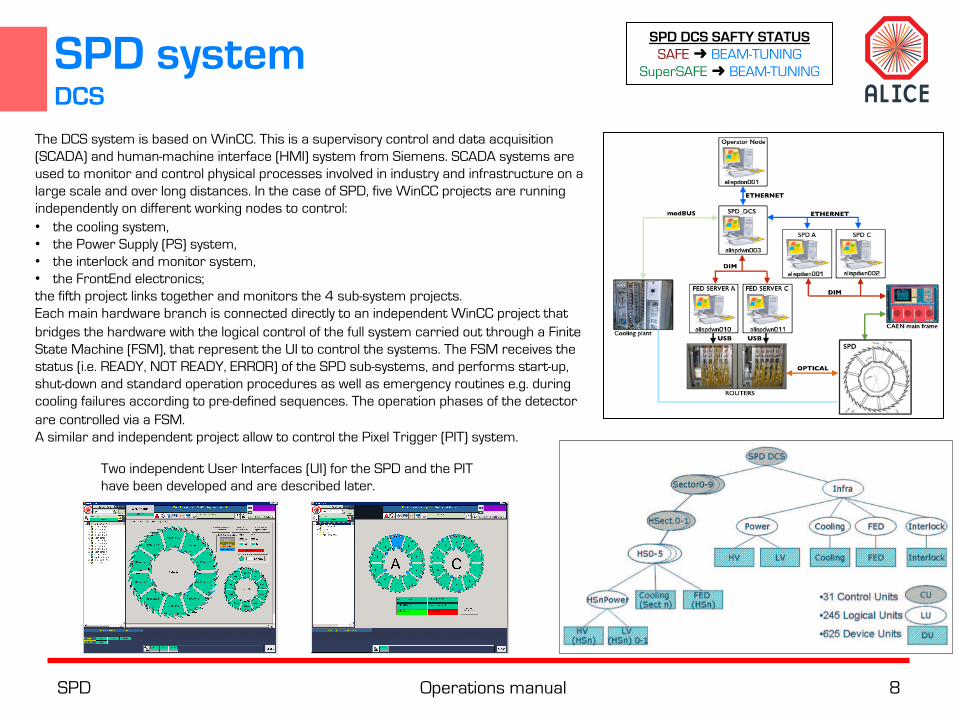
SPD system DCS
The DCS system is based on WinCC. This is a supervisory control and data acquisition (SCADA) and human-machine interface (HMI) system from Siemens. SCADA systems are used to monitor and control physical processes involved in industry and infrastructure on a large scale and over long distances. In the case of SPD, five WinCC projects are running independently on different working nodes to control: • the cooling system, • the Power Supply (PS) system, • the interlock and monitor system, • the FrontEnd electronics; the fifth project links together and monitors the 4 sub-system projects. Each main hardware branch is connected directly to an independent WinCC project that bridges the hardware with the logical control of the full system carried out through a Finite State Machine (FSM), that represent the UI to control the systems. The FSM receives the status (i.e. READY, NOT READY, ERROR) of the SPD sub-systems, and performs start-up, shut-down and standard operation procedures as well as emergency routines e.g. during cooling failures according to pre-defined sequences. The operation phases of the detector are controlled via a FSM. A similar and independent project allow to control the Pixel Trigger (PIT) system.
Two independent User Interfaces (UI) for the SPD and the PIT have been developed and are described later.
SPD DCS SAFTY STATUS SAFE ➜ BEAM-TUNING
SuperSAFE ➜ BEAM-TUNING
SPD Operations manual 9
SPD system DAQ
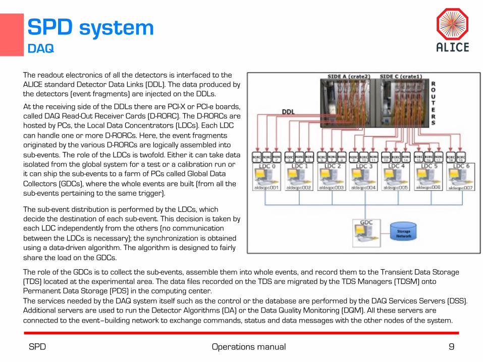
The readout electronics of all the detectors is interfaced to the ALICE standard Detector Data Links (DDL). The data produced by the detectors (event fragments) are injected on the DDLs.
The role of the GDCs is to collect the sub-events, assemble them into whole events, and record them to the Transient Data Storage (TDS) located at the experimental area. The data files recorded on the TDS are migrated by the TDS Managers (TDSM) onto Permanent Data Storage (PDS) in the computing center. The services needed by the DAQ system itself such as the control or the database are performed by the DAQ Services Servers (DSS). Additional servers are used to run the Detector Algorithms (DA) or the Data Quality Monitoring (DQM). All these servers are connected to the event–building network to exchange commands, status and data messages with the other nodes of the system.
At the receiving side of the DDLs there are PCI-X or PCI-e boards, called DAQ Read-Out Receiver Cards (D-RORC). The D-RORCs are hosted by PCs, the Local Data Concentrators (LDCs). Each LDC can handle one or more D-RORCs. Here, the event fragments originated by the various D-RORCs are logically assembled into sub-events. The role of the LDCs is twofold. Either it can take data isolated from the global system for a test or a calibration run or it can ship the sub-events to a farm of PCs called Global Data Collectors (GDCs), where the whole events are built (from all the sub-events pertaining to the same trigger).
The sub-event distribution is performed by the LDCs, which decide the destination of each sub-event. This decision is taken by each LDC independently from the others (no communication between the LDCs is necessary); the synchronization is obtained using a data-driven algorithm. The algorithm is designed to fairly share the load on the GDCs.
SPD Operations manual 10
SPD system PixelTrigger (PIT)
To DAQ passing through the ROUTERS
10 algorithms
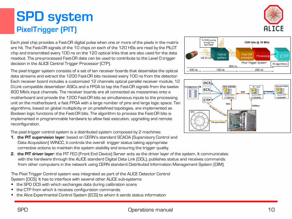
The pixel trigger system consists of a set of ten receiver boards that deserialize the optical data streams and extract the 1200 Fast-OR bits received every 100 ns from the detector. Each receiver board includes a customized 12 channels optical parallel receiver module, 12 G-Link compatible deserializer ASICs and a FPGA to tap the Fast-OR signals from the twelve 800 Mb/s input channels. The receiver boards are all connected as mezzanines onto a motherboard and provide the 1200 Fast-OR bits as simultaneous inputs to the processing unit on the motherboard, a fast FPGA with a large number of pins and large logic space. Ten algorithms, based on global multiplicity or on predefined topologies, are implemented as Boolean logic functions of the Fast-OR bits. The algorithm to process the Fast-OR bits is implemented in programmable hardware to allow fast execution, upgrading and remote reconfiguration.
The pixel trigger control system is a distributed system composed by 2 machines: 1. the PIT supervision layer: based on CERN’s standard SCADA (Supervisory Control and
Data Acquisition) WINCC, it controls the overall trigger status taking appropriate corrective actions to maintain the system stability and ensuring the trigger quality.
The Pixel Trigger Control system was integrated as part of the ALICE Detector Control System (DCS). It has to interface with several other ALICE sub-systems: § the SPD DCS with which exchanges data during calibration scans § the CTP from which it receives configuration commands § the Alice Experimental Control System (ECS) to whom it sends status information
Each pixel chip provides a Fast-OR digital pulse when one or more of the pixels in the matrix are hit. The Fast-OR signals of the 10 chips on each of the 120 HSs are read by the PILOT chip and transmitted every 100 ns on the 120 optical links that are also used for the data readout. The pre-processed Fast-OR data can be used to contribute to the Level 0 trigger decision in the ALICE Central Trigger Processor (CTP).
2. the PIT driver layer: the PIT FED (Front End Device) Server acts as the driver layer of the system. It communicates with the hardware through the ALICE standard Digital Data Link (DDL), publishes status and receives commands from other computers in the network using CERN standard Distributed Information Management System (DIM).
SPD Operations manual 11
Operations Overview
q Operate the SPD [Slide 12] ü SPD UI and how to log on it ü FSM structure and how to take/release the its control ü How to restart the FSM ü How to unlock the FSM by force ü FSM padlock status color code ü FSM components status color code ü Correspondence between FSM status and hardware powering ü How to switch ON the detector from scratch ü How to switch ON a half-stave that unexpectedly went OFF ü How to switch OFF the detector or a half-stave ü How to release half-stave in error status ü How to clear CAEN alarms ü How to clean the DSS interlocks ü How to include/exclude a component in the FSM ü How to mask a noisy pixel ü Chips configuration (check conf. in the hardware) ü How to link the last configuration version inside ACT
q Operate the PIT [Slide 18] ü PIT UI and how to log on it ü How to load the PIT configuration(s) from the database ü How to exclude chip(s) from the link configuration ü How to restart the phase alignment service ü How to link the configuration version inside ACT
q Taking data [Slide 21] ü How to get the detector READY for a global run ü How to open the DAQ software in the SPD station ü How to launch a run in standalone ü How to check the list of HSs included in data-taking ü How to exclude a full router from data-taking
q What to do when… [Slide 24] ü What to do when a half-stave goes “HOT” ü What to do when the SPD FED servers goes down ü What to do when the phases are not aligned ü What to do when SPD_RUN or spdFEElectronics are not READY ü What to do when a CDH error occur
q For experts [Slide 27] ü How to transfer file(s) from/to P2 ü How to obtain the SPD FED log ü How to start and use the Error Handler ü What to do in case an HS goes HOT for expert ü How to get and change the DSS interlock temperature ü How to deal with the FED server and the router crate ü How to determine the channel not aligned in the PIT ü How to set and read the output algorithm parameters ü How to pen the PIT FED log ü How to restart the PIT FED driver ü PIT algorithm description ü PIT algorithm parameters description ü How to operate the cooling plant ü How to program the Routers permanently and temporary ü How to handle the DSS alarms ü How to control the CAEN main frame using telnet ü How to execute TTCinit and ttcFEEreset from LTU client ü How to modify the detector file in the DAQ
SPD Operations manual 12
Operations Operate the SPD (1/6)
SPD UI AND HOW TO LOG ON IT Start an Xterm window and connect to the operator node giving the following command after the prompt: ‘rdesktop –a16 –g3800x1100 alispdon001 &’ and click return. The input “3800x1100” defines the screen size (double screen in this case); use 1900x1100 in case of single screen. Login using your NICE username and password. The SPD user interface (UI) opens automatically and to login the relative "SPD” user and password are requested. In case the User Interface does not automatically open or the panel is closed by mistake, users should go to Windows start menu and click “spdUserInterface.exe”.
In the picture the most relevant components of the SPD UI are identified : 1) The FSM button -- Opens the FSM control panel 2) SPD status – Reports the status of the SPD FSM top node 3) User logged – Declares the user actually logged (usually spd as seen before) 4) Log in button – If the login panel do not open automatically can be opened from this
button 5) FSM control status – Declares the status of the FSM main padlock or of the
component selected in the DCS tree 6) FSM tree -- From here it is possible to navigate through the components of the FSM 7) Detector Monitoring Zone – Reports the status for the nodes of the services 8) Distributed system status – Reports the status of DCS PCs 9) Main control panel – A sketch of the detector (two sides) gives the status of each
HS 10) Alarm panel – Gives access to the DSS alarm panel (read only) 11) HS condition panel – Allow to query a list of general parameters for all the HSs 12) Temperature trend panel – Allow to display the temperature trend of the HSs for
each sector 13) GoSafe button -- Forces the status from “READY” to “BEAM_TUNING” 14) FED status – Declares the status of the service in the two FEDs 15) Running status – Declares if the SPD is included in a run (global or standalone) 16) DSS interlock status – Reports the status of the active DSS interlocks 17) DSS status – Declares the status of the DSS system
SPD Operations manual 13
Operations Operate the SPD (2/6)
FSM STRUCTURE AND HOW TO TAKE/RELEASE ITS CONTROL The FSM is divided in 12 branches (or nodes): 10 for the control of the sectors, 1 for the services and 1 for the readout front-end electronics. The 10 branches for the sectors are sub-divided in 2 branches for the two sides and then in 6 branches for the HSs. The services branch is sub-divided in three branches: SPD_VME, Spd_Power and SpdCooling. The control of the FSM is regulated by a padlock ownership system. To gain control of the FSM: press the FSM button on UI, top left, to open the FSM control panel, press the padlock button in the top line and select TAKE/REALEASE in the menu.
HOW TO RESTART THE FSM Open the main FSM panel from the button at the bottom of the User Interface (the one with the tools symbol on it, see picture). Click on the big ”START/RESTART all" button in the middle of the panel. After the restart the lock is open by default. In case there was an error with the FSM lock, the control can be gained again from here.
HOW TO UNLOCK THE FSM BY FORCE Open the FSM control panel (top left part of main UI panel). Click on the top node padlock; it will appear a small gray window. Click with the right button of the mouse in this window; it will appear a small button ‘Expert Menu’. Click on it and then click on ‘FORCE RELEASE’.
FSM PADLOCK STATUS COLOR CODE GREY: No one has control of the FSM. No commands can be issued. GREEN: The SPD user has exclusive control over the FSM and only him/her can issue commands. RED: The FSM is operated in exclusive mode by another PC. Commands may not be issued from the SPD user’s PC. YELLOW: The partition is shared but not operated by the SPD user’s PC. All the same, SPD users and others may issue commands. BLUE: the partition is shared and operated by the SPD user’s PC. SPD users and others may issue commands.
FSM COMPONENTS STATUS COLOR CODE GREY: excluded part or dead GREEN: READY status RED: ERROR status YELLOW: temporary status (moving up or down) BLUE: OFF, MCM_only, STBY_CONFIG or BEAM_TUNING status ORANGE: warning status
CORRESPONDENCE BETWEEN HS FSM STATUS AND HARDWARE POWERING HS powering status corresponding to the FSM status:
READY: inverse bias applied to the sensor (HV power: 50 V) BEAM_TUNING: MCM chip and bus ON (LV power: 2.6 V and 1.8V) STBY_CONFIG: equivalent to the previous MCM_only: only MCM chip ON (LV power: 2.6 V) OFF: all the components are OFF
SPD Operations manual 14
Operations Operate the SPD (3/6)
HOW TO SWITCH ON THE DETECTOR FROM SCRATCH ① Select the top node (SPD_DCS) before opening and gain control of the FSM ② Switch on FEE: in the FSM panel select SpdServicesàSpdVME and select SWITCH_ON for the two crates (top left picture) ③ Switch on power supply: in the FSM panel select SpdServicesàSpdPower and SWITCH_ON for SY1527 and the two
channel000 and channel 001 (top left picture) ④ Open the cooling lines, if the plant is running: these have to be opened waiting the flow to stable in one line before opening
the following (top left picture) ⑤ Clean the DSS interlocks for all the cooling lines. If all lines are open and all the interlocks are cleared, on the main
SPD_DCS panel the DSS Interlock status indicator has to be green. ⑥ Clean the CAEN alarms ⑦ If also the routers switched off, open Manual ConfigàRouter settingsàPanels for expertsàInitialize routers and initialize
all routers; also click on Manual ConfigàRouter settingsàRESET TTCrx to reset the TTCrx chip (top right picture) ⑧ Make sure that the good configuration is loaded. Go to SPDFEElectronics and click on LoadConfiguration button, click on
Load detector config, select the last version and click SELECT (mid picture) ⑨ Check in the FSM that all the HSs that have to be switched ON are actually included; we usually move to READY only HSs
that have to be included in data-taking, all the other stay in MCM_ONLY. ⑩ The following steps have to be applied to all the HSs that the user wants to move READY:
1) open the branch of the semi-sector of interest in the FSM tree 2) keep always open the AutomaticConfig panel (button available on the right part of the panel) 3) open the FSM control and, for the HS to be switched on, select GO_MCM_ONLY from the pull-down menu (this
command can be given for all half staves of the same semi-sector at once from the semi-sector top node) 4) from the MCM_ONLY state select the command GO_STBY_CONFIGURED from the pull-down menu in the FSM
control (this command have to be given to the single HS) 5) immediately when the status STBY_CONFIGURED is reached (FSM status is blue) click on Config HS in the Automatic
config panel, where you have already selected the HS to configure 6) repeat the previous two actions for all the HSs of the semi-sector; when all the HSs are in the STBY_CONFIGURED
status, give the command GO_BEAM_TUNING and then GO_READY to all of them at once from the semi-sector top node.
Alternatively, the user can chose to give the command GO_STBY_CONFIGURED to all the HSs at once. In this case the operator have to be very fast giving the configuration to all the active HS from the AutomaticConfig panel. A led became green if the configuration went OK. In case of failure it became red. In this case: 1. click on “Reset R. Channels” and “Jtag IR reset” buttons, in the same panel and try again 2. check that the HS is in BEAM_TUNING and is not in the list of problematic modules
SPD Operations manual 15
Operations Operate the SPD (4/6)
HOW TO SWITCH ON AN HALF-STAVE THAT UNEXPECTEDLY WENT OFF This procedure is useful e.g. when an HS switched OFF for whatever reason (HOT, ITR, etc.); in these cases, the HS is usually in ERROR status. A cleaning procedure for the alarms have to be followed (will be described in a future section). After the cleaning of the alarms, the status of the HS is usually, MCM_ONLY. This is the starting point we assume: ① Open the SPD_DCS branch of the semi-sector of interest ② Keep always open the "AutomaticConfig” panel (button available on the right part of the panel) ③ Open the FSM panel to the node corresponding to the HS to be switched ON ④ Select the command GO_STBY_CONFIGURED from the pull-down of the considered HS ⑤ Immediately when the status STBY_CONFIGURED is reached (FSM status is blue) click on "Config HS" in the ”Automatic config” panel, where
you have already selected the HS to configure ⑥ Select the command GO_BEAM_TUNING from the pull-down of the considered HS ⑦ Select the command GO_READY from the pull-down of the considered HS
HOW TO SWITCH OFF THE DETECTOR OR AN HALF-STAVE The following procedure could be needed in case of hardware interventions on the detector. We start from the assumption that the HS(s) is(are) in READY status when starting the procedure: ① Select the top node (SPD_DCS) before opening and gain control of the FSM ② Open the FSM panel to the node corresponding to the concerned HS ③ Select the command GO_BEAM_TUNING from the pull-down of the considered HS (this command can be sent from the detector top node to all
the HSs contemporary) ④ Wait until the the status BEAM_TUNING is reached and select the command GO_STBY_CONFIG from the pull-down menu of the considered HS
(this can be sent from each sector top node); it is immediate since don’t underlie any change in the voltage but simply a DCS status change ⑤ When the HS(s) is(are) in STBY_CONFIG, select the command GO_MCM_ONLY from the pull-down menu of the considered HS (this can be
sent from each sector top node) ⑥ When the HS(s) is(are) in MCM_ONLY, select the command GO_OFF from the pull-down menu of the considered HS (this can be sent from
each sector top node) Depending on the foreseen hardware intervention also the powering, the fee and the cooling plant could be switched off: • Switch off the FEE: in the FSM panel select “SpdServices”à“SpdVME” and select “off” • Switch off the power supply: in the FSM panel select “SpdServices”à“SpdPower” and move off all the components • Close the cooling lines, and leave the plant running
SPD Operations manual 16
Operations Operate the SPD (5/6)
HOW TO RELEASE AN HALF-STAVE IN ERROR STATUS One or more HSs could run into ERROR for different reasons. As a first action when a failure happens, it is fundamental to identify the HS(s) that suffered the failure and the reason for it; these details have to be reported in the logbook entry concerning the failure.. To release the error: ① go to SPD_DCS node corresponding to the sector with the HS in ERROR and click on "Clear CAEN alarms”. ② go to the FSM node corresponding to the HS in ERROR and in the pull-down menu select RELEASE ③ check that in the FSM the HS goes to a safe blue status
HOW TO CLEAN THE CAEN ALARM This operation is needed every time has been removed at least one interlock or in case some module suffer a HV TRIP. Open the branch SPD_DCS/SpdServices/SpdPower/SY1527 and click the “Clear Alarms” button (bottom right). The same button is present in every SPD_DCS -sector panel (bottom right).
HOW TO CLEAN THE DSS INTERLOCKS The Detector Safety System panel is always open in a PC close to the DCS station. In the panel, the detector and the device names are in the 2nd column; the 3rd column shows the logic name which is useful to understand where in the detector the problem has occurred; the 4th column provides a short description of the kind of error that has occurred. To clear an alarm, click on its name
HOW TO INCLUDE/EXCLUDE A COMPONENT(S) IN THE FSM The most frequent case is when an HS has to be excluded from the data-taking because of problems. In the FSM the status of a node (a component) is propagated to the top node; to take data, the top node of the SPD has to be READY (in case of physics partition) or BEAM_TUNING/READY (in case of technical partition). If one component goes in ERROR this error is propagated to the top node; once the ERROR status is released, the FSM top node will probably be in a MIXED status, since the problematic HS will probably be in MCM_ONLY. If the HS cannot be recovered it has to be excluded from the FSM. From the FSM, in correspondence of each HS there is a button with a tick symbol; clicking on it a panel opens, where the only button allow to enable/disable the corresponding node. Remember that the SPD is also a trigger detector; every time you exclude a component from the data-taking be sure that the corresponding chips are excluded from the trigger mask.
SPD Operations manual 17
Operations Operate the SPD (6/6)
HOW TO MASK A NOISY PIXEL The presence of a noisy pixel could affect both the hit maps and the trigger rate; therefore it is important to monitor the presence of noisy pixel and mask it as soon as possible (this has to be agreed with the RC usually, depending on the data-taking condition). In the spdFEElectornics FSM node click on button “Show pixel mask” (see picture). In the new panel select the sector/side/half-stave/chip/column/row of the pixel that has to be masked and click on “Insert Noisy Pixel”; a new line will be added in the list. Once all the noisy pixels have been inserted, click on “Mask Detector”: a new version of the mask will be created and the new mask will be applied to the hardware. The last loaded mask version number can be read in the top part of this panel.
CHIPS CONFIGURATION AND HOW TO CHECK THE VERSION LOADED IN THE HARDWARE The front-end chip has many parameters: 42 8-bit DACs that can be individually tuned for the detector operation and optimization; they act, for example, on voltage and current references, delays and readout threshold. Other parameters allow to configure the MCMs and the routers. As seen, from the Load Configuration the value of the DAC and MCM parameters can be loaded in the FED. The version number of the configuration actually loaded in the FED can be retrieved using the button SPS VerNum in the spdFEElectronics node in the FSM tree. In the Load Configuration panel, it is possible to compare the configuration present in the hardware with one from database or compare two different versions from database.
HOW TO LINK THE LAST CONFIGURATION VERSION INSIDE ACT When a new configuration is created, it is needed to register it as the default one, in the ALICE Configuration Tool (ACT): 1) click on the FERO CC button (top right, with the tools icon) 2) specify that a DB version can be considered as good (and linkable):
2.1) click on "Allowable versions" and select the version that you want to link. BE CAREFUL: the versions are not ordered by number 2.2) insert a Description and click on "Set version as allowable"
3) now link this version to the correct run type: 3.1) click on "Current versions” 3.2) select the run type (usually PHYSICS, but we usually do it also for all the other) and click on Modify 3.3) It's not necessary to specify any parameter, select the version from the "Allowable versions" table and click on "Set as current version” 3.4) exit from the panel and check with the refresh button that everything is correct
4) check that the configuration went fine, looking at the table in the Current versions tab
SPD Operations manual 18
Operations Operate the PIT (1/3)
PIT UI AND HOW TO LOG ON IT The PIT User Interface is accessible from the same operator node (alispdon001) where the SPD UI is accessible, clicking on the corresponding icon on the desktop. The SPD account has to be used to login. As for the SPD UI, we do have a FSM tree and a corresponding FSM control panel, through which send the commands. The nodes of the FSM tree are:
-- PitLINK_STATUS: contains the status of the 120 links between the HSs and the PIT; it is subdivided in 10 sub-nodes, each subdivided in 2 sub-nodes (side A and C). A schematic representation of the PIT links is available in the main PIT_DCS panel, useful to have a quick status of the links. Each link can be: GREEN (READY) HS in ready state and included in the trigger logic, BLUE (NOT REQUIRED) HS masked in the trigger logic (they can be both switched on or off), or ORANGE (NOT LOCKED) HS not switched on but required from the trigger logic.
-- PitVME: contains few monitoring panels for the hardware, like VME crate powering. -- PitFED: contains only one node, the one fundamental for the configuration of system.
The PitFED panel contains 5 tabs (from left to right): -- Proc Counters [1]: allow to configure the 10 outputs in 4 configurations (NORMAL,
TOGGLE, SIGNATURE, RANDOM) useful for CTP test and to configure the 10th output, the one usually used for cosmic trigger.
-- Link settings [2]: allow to set the mask for the chips in each HS and check the noise through a counter.
-- Configuration [3]: the most useful panel, needed to give the configurations to the systems through three buttons available at the center of the panel.
-- Advanced Panel [not shown]: allow advanced functionality, not useful for the normal operation.
-- Monitor Counters [4]: allow to check the rates for all the 10 outputs.
1 2
3 4
SPD Operations manual 19
Operations Operate the PIT (2/3)
HOW TO LOAD THE PIT CONFIGURATION(S) FROM THE DATABASE The PIT database contains 3 different sets of configuration: -- FIRMWARE: definition of the algorithms associated to the 10 outputs, and of their
parameters. -- PARAMETERS OF ALGORITHMS: definition of the values of the algorithm parameters. -- MASK: definition of the trigger mask (map of the chips that contribute to the trigger). These 3 information can be treated separately, through the “Configuration” tab in the “pitFedStatus” panel, under the PitFED node. The procedure to retrieve a configuration is similar in the 3 cases: ① click on the button of the needed configuration, a new panel will open ② press the button “Select a Version” in the new panel, a new panel will open ③ choose one version from the database clicking two times on it, this panel will close ④ click on "Apply DB Version To The Hardware” button
HOW TO EXCLUDE CHIP(S) FROM THE LINK CONFIGURATION This could be needed if an HS is excluded from the data-taking or a single chip is too noisy to be included in the trigger mask. ① from the PIT_DCS menu open the node PitFEDàpitFedStatusàConfiguration ② press on the button "Link DB Configuration", a new panel will open ③ press on the button "Select a Link Version" and choose one database version to load (usually the most recent) ④ apply the desired changes: the chips included in the trigger logic are with a tick mark, the masked chips correspond to empty boxes ⑤ once finished, click on "Apply data from panel to the hardware”. Eventually, when the changes are fully checked, create a new DB version by clicking on the button "Create new version from the hardware”.
If a modification has been applied to the loaded DB version, the parameter present in the panel can be directly applied to the hardware through the button “Apply data from panel to the Hardware”. If a new version of the configuration actually present in the hardware has to be created click on “Create New Version From Hardware”. Remember to create a new version of each configuration every time the value of a parameter is changed; it is important to know which configuration is used when taking data, so keep track of it.
SPD Operations manual 20
Operations Operate the PIT (3/3)
HOW TO RESTART THE PHASE ALIGNMENT SERVICE The 1200 Fast-OR signals have to arrive synchronized to the PIT so ad-hoc delays are applied to the 120 optical links. A service check constantly the alignment of the phases at the PIT. Two LEDs in the main PIT_DCS show the status of the service and the status of the phases (see picture). If, during a run, the service the check the phases alignment stop to work, the corresponding indicator became red and a message appears in the central DCS station. If this happen: -- go to the PIT_DCS main panel and click on "Restart Phases Service” button
HOW TO LINK THE CONFIGURATION VERSION INSIDE ACT When a new configuration is created, it is needed to register it as the default one, in the ALICE Configuration Tool (ACT). As already said we do have three different configurations in the PIT. The procedure is the same for all of them and the same as for the SPD. 1) click on FERO CC button (top right, with the tools icon) 2) from the Detector menu choose PIT 3) specify that the new configuration version can be considered as good (and linkable) 3.1) click on "Allowable versions” button 3.2) from the Subsystem menu choose Firmware Configuration, Firmware parameters or Link configuration depending on the version you
want to link (usually it is Link configuration) 3.3) select the version that you want to link from the list on the left (observe that are not in order) 3.3) insert a Description and click on "Set version as allowable" 4) now link this version to the correct run type 4.1) click on "current versions" 4.2) select the run type (usually PHYSICS, but we usually do it also for all the other) and click on Modify 4.3) from the Subsystem menu choose Firmware Configuration, Firmware Parameters or Link Configuration 4.4) choose also the Parameter value: the following action have to be done for the possible parameter value 4.4) select the version from the "Allowable versions" table and click on "Set as current version" 4.5) exit from the panel and check with the refresh button that everything is correct 5) check that the configuration went fine, looking at the table in the Current versions tab
SPD Operations manual 21
Operations Taking data (1/3)
HOW TO GET THE DETECTOR READY FOR A GLOBAL RUN Before the final configuration of the detector the following checks have to be done: -- the SPD_DCS and the PIT_DCS top nodes have to GREEN (READY) -- the DAQ and DCS locks are taken by the central systems -- only the working HSs have to be included in the data-taking -- the correct SPD configuration is loaded in the hardware -- if all the HSs in a Router are excluded make sure that you have followed the procedure to
exclude the router from the data taking The following procedure has to be followed for the final configuration of the detector (all the following actions are performed from the spdFEElectornics panel in the DCS UI): ① “Hardware synchronization” button [1] - ② “Refresh ChList” button [2] – Update the list of the HS included in data-taking in the FED ③ “AutoConfig Router” button [3] – Configure the routers with the chosen configuration ④ “Reset DPI for all” button [4] – Reset the data points in the routers ⑤ “Data Reset for all” button [5] – Reset all the data in the routers ⑥ “AutoConfig Router” button [3] -- Configure the routers with the chosen configuration ⑦ “Config HS List” button [6] – Configure the HS ⑧ “Mask SPD” [7] – Apply the noisy pixel mask
[1] [2] [3]
[4] [5]
[6] [7]
Numbers in parenthesis refer to what reported in the picture. Each button has a corresponding led to confirm the success of failure of the action. These actions have to be performed after whatever intervention on the detector or after a long period of inactivity before the start of the run. Notice a similar sequence of actions is automatically performed at the beginning of each run, so it is not needed to be manually performed before each runs. It is probably better to perform it before the start of the first run of the fill.
SPD Operations manual 22
Operations Taking data (2/3)
HOW TO OPEN THE DAQ SOFTWARE IN THE SPD STATION In the ARC working ambient (when accounted with the SPD credential) it is available the DAQ system dedicated to our detector (equivalent to the one available in the central station). An icon is present in the top bar of the operating system; a small window open and the only option is “SPD”. Four windows are displayed: the Detector Control Agent (DCA), the main ECS window and the infoBrowser. These panels allow to configure the detector for data taking. The DCA panel allows to gain control of the detector and to work on the acquisition system (i.e. chose the kind of run). The experiment control system (ECS) panel allows to check the read-out status and to configure the data acquisition system (i.e.: equipment selection). Through the Info Browser panel it is possible to check the state of the run and to publish and read an error list in case any fault should occur.
HOW TO LAUNCH A RUN IN STANDALONE MODE Similar recommendations as given for the case of a run in global partition are valid in this case. How to start a standalone run: ① Start the DAQ system and gain control of the detector from the DCA panel ([1] in the picture); the
padlock has to closed and green. ② Click “select equipment” on the main ECS panel; in the window chose the routers to exclude/include in
the run according to the detector status and don’t forget to “commit”. ③ Click “View” on the DCA panel and select “show DAQ control” from the pull-down menu. ④ Release the DAQ_RC padlock in the DCA panel and gain the padlock in the DAQ Run Control panel ⑤ Click “Define” in the DAQ Run Control ([2] in the picture) and select the LDC; normally all of them are
active. ⑥ Click sequentially on the arrows present in the DAQ Run Control ([3] and [4] in the picture). ⑦ Release the padlock in the DAQ Run Control and gain back the DAQ_RC padlock in the DCA ⑧ In order check the status of the run (rates, LDCs, number of events...) two more panels can be
opened from the DAQ Run Control “View” menu: …... . ⑨ Make sure that the padlocks displayed on the DCA panel are green, then click on the “DCA” button
([3] in the picture) and select the kind of run to be started. Two kind of standalone runs can be performed: -- Bunch Crossing (BC) : the trigger is randomly given by the CTP and the rate can be selected; -- Pulser : the trigger is given by the PIT and can be used to check the presence of noisy pixels, the
acquisition rate, and to do perform uniformity scan.
SPD Operations manual 23
Operations Taking data (3/3)
HOW TO CHECK THE LIST OF HSs INCLUDED IN DATA-TAKING In the first two steps of the procedure to make the detector ready for data-taking, the list of active HSs in the FEDs is aligned to the status of the hardware; only HS that are at least in BEAM_TUNING status are activated. Also in this panel are available the two buttons “Hardware synchronization” and “Refresh ChList”.
HOW TO EXCLUDE A FULL ROUTER FROM DATA-TAKING In case all the 6 HSs in a semi-sector have to be excluded from data-taking few more actions have to be performed in order to communicate to the DAQ to not wait any data from the corresponding DDL: ① go to Manual configàRouter settings in FEElectronics node of the FED tree ② select the router that has to be excluded ③ tick "Exclude trigger from TTC" and "High multiplicity in CDH" and click "write” ④ go to Manual configàFanInFanOut ⑤ untick to remove the router you want to exclude, click on write and then read
for confirmation During Run1, it was also needed to remove in the DAQ the corresponding equipment in the DCA; during Run2 this procedure has been made automatic.
SPD Operations manual 24
Operations What to do when… (1/3)
WHAT TO DO WHEN AN HS GOES HOT OR IN CASE OF TEMPERATURE WARNING When a HS gets HOT the interlock system switches it off thus safeguarding the detector. To continue the data taking it is fundamental to remove the error from the FSM to node: ① from the SPD UI main panel, click on the HS in error state à a new panel opens, with the control of this HS (no need to ask it to the DCS) ② release the error à the HS will automatically go to MCM_ONLY state Before to decide to exclude this HS, it could be worth to try to recover it: • try to switch it on again (remember perform the procedure do get the detector ready for the data taking) If the HS has to be excluded: • leave it in MCM_ONLY status • exclude the corresponding node in the FSM If all the HS of one router are excluded from the FSM, follow the procedure to exclude the router from the data taking. If a software interlock happened, all the HS of the router will be switched off and a CAEN interlock will appear; in this case clear the alarms from the DSS station and switch on the HSs again.
WHAT TO DO WHEN THE SPD FED SERVERS GOES DOWN The status of the FED services can be monitored looking at the two LEDs, side A and C, in the SPD UI main panel. If the two LEDs are green, the services are running fine; if they became red, the corresponding service needs to be restarted. The procedure is: ① rdesktop to alispdwn010 and alispdwn011 ② Start à Administrative tools à Services in the Windows panel ③ stop and start the spdfed_server service ④ go back to SPD UI
• Refresh ChList + AutoConfig Router + Load DB Configuration + Config HS List + Mask SPD If the previous procedure do not help and the PC needs to be restarted: ① go to Start à Accessories à Command prompt and type "shutdown -r -t 01” ② the PC will restart, then do actions from 2 to 4 For your info, the executable is in D:\spdFed\SPD_FEDServer.exe.
SPD Operations manual 25
Operations What to do when… (2/3)
WHAT TO DO WHEN SPD_DCS_RUN or spdFEElectronics are not READY Rarely, after a run ended in a bad way, the SPD_DCS_RUN or spdFEElectronics can bacome not READY and the possibility to start a new run is inhibited. To solve this: ① open the FSM control panel from the top node ② for the node spdFEElectronics select "Configure” ③ for the node SPD_DCS_RUN select "EOR” (leave the dialog box empty) ④ look at the LogFed displays in the spdFEElectronics panel and any errors occur ⑤ if all go fine, give the command "Allow Run" from the SPD_DCS_RUN node in the FSM control panel ⑥ add a logbook entry
WHAT TO DO WHEN THE PIT PHASES ARE NOT ALIGNED Two LEDs in the main PIT_DCS show the status of the service and the status of the phases (see picture). If the "Check Phases” LED is red: ① check the “Phases service OK” LED on the main PIT panel ② if the indicator is red the service is not work and needs to be activated If, when the service is working, the phases are not aligned
• call the expert • write an entry in the Logbook
The run needs to be stopped only if the SPD is included in the trigger. Note that out of a run the phases could be not aligned, but the service have to be always running.
To be verified
SPD Operations manual 26
Operations What to do when… (2/3)
To be finished
WHAT TO DO WHEN A CDH ERROR OCCUR The num
SPD Operations manual 27
Operations For experts (1/9)
TRASFER A FILE OUT OF P2 OR VICEVERSA One has to use the DAG gateway and the AFS public folder A. From outside to P2
① copy the file on lxplus ② from the PC in the ARC: scp dcolella@aldaqgw01-daq02:afs/cern.ch/user/d/dcolella/public/[file] ./
B. From P2 to outside ① copy the file from the PC in the ARC to lxplus: scp [file] dcolella@aldaqgw01-daq02:afs/cern.ch/user/d/dcolella/public/
TRASFER A FILE FROM SPD DCS OPERATOR NODE TO OUTSIDE In alispdon001, START à Search programs and files à “\\alidcsfs001”. Copy the file in the folder “\Scratch_data\spd\” From the mac connect to: smb://aldcsfs001.cern.ch (account NICE)
HOW TO OBTAIN THE SPD FED LOG In the PC alispdon001, click on the START button and type a double slash (“\\”) in the “Search programs and files”; a list with three link will appear. Choose one between: alidcscom904 and alidcscom905 (the two SPD FED servers). A folder will open. Choose the sub-folder ‘spdFED’. Here many files called ‘spd – xx.xx.xxxx’ are store: the one without date is the current one.
SPD Operations manual 28
Operations For experts (2/9)
HOW TO START THE ERROR HANDLER Full description of the system can be found here: https://drive.google.com/open?id=0B5nG1xNTPzEJd2ZJejVlQV90Rlk. To activate the process: ① be sure that the SPD is not in data taking! ② go to spdFEElectronics à Manual config à Router settings ③ click on "no data to DAQ" and "High multiplicity in CDH” ④ click on "write all active” ⑤ open Panel collection for experts à Router error mask ⑥ click on "Set to all", "Enable all errors", "Fastor errors in the data stream" and "Longer busy error” ⑦ click on "Write", check with "Read” ⑧ go to spdFEElectronics à Manual config à Router settings ⑨ Un-tick "no data to DAQ" and click "write all active” If the Error Handler is active, in theFedLog displays in the SpdFEElectronics node, there can be log lines with the message "INFO: ERROR HANDLER - router XX with XX errors during last pooling”. They are not a real error, nothing has to be done, just ignore it.
HOW TO USE THE ERROR HANDLER The Error Handler panel can be reached from the spdFEElectonics node through the button “Router Errors”; a new panel will be opened. In this panel one could specify: Run number, Router Number, Error Class Name and launch a query through the button “Errors general Query”. Once the query is over the message “Query executed” appears in the displayer “Messages”. The query could take also few minutes. Usually one has an end of run reason (EOR) due to the SPD and want to verify the origin of the EOR trying to identify the HS responsible for the error: in this case one has to insert the run number in the corresponding slot and launch the query. How to read the output of the query will be described in the data monitoring section.
SPD Operations manual 29
Operations For experts (3/9)
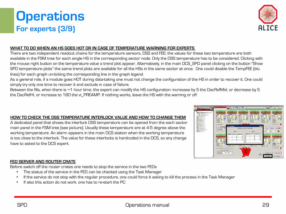
HOW TO CHECK THE DSS TEMPERATURE INTERLOCK VALUE AND HOW TO CHANGE THEM A dedicated panel that shows the interlock DSS temperature can be opened from the each sector main panel in the FSM tree (see picture). Usually these temperature are at 4-5 degree above the working temperature. An alarm appears in the main DCS station when the working temperature is too close to the interlock. The value for these interlocks is hardcoded in the DCS, so any change have to asked to the DCS expert.
WHAT TO DO WHEN AN HS GOES HOT OR IN CASE OF TEMPERATURE WARNING FOR EXPERTS There are two independent readout chains for the temperature sensors, DSS and FEE; the values for these two temperature are both available in the FSM tree for each single HS in the corresponding sector node. Only the DSS temperature has to be considered. Clicking with the mouse right button on the temperature value a trend plot appear. Alternatively, in the main DCS_SPD panel clicking on the button "Show SPD temperature plots” the same trend plots are available for all the HSs in the same sector at once. One could disable the TempFEE (blu lines) for each graph un-ticking the corresponding line in the graph legend. As a general role, if a module goes HOT during data-taking one must not change the configuration of the HS in order to recover it. One could simply try only one time to recover it and exclude in case of failure. Between the fills, when there is ~1 hour time, the expert can modify the HS configuration: incresase by 5 the DacRefMid, or decrease by 5 the DacRefHi, or increase to 180 the vi_PREAMP. If nothing works, leave the HS with the warning or off.
FED SERVER AND ROUTER CRATE Before switch off the router crates one needs to stop the service in the two FEDs
• The status of the service in the FED can be checked using the Task Manager • If the service do not stop with the regular procedure, one could force it asking to kill the process in the Task Manager • If also this action do not work, one has to re-start the PC
SPD Operations manual 30
Operations For experts (4/9)
HOW TO DETERMINE THE CHANNEL NOT ALIGNED IN THE PIT The values for these delays have been measured and do not need to be changed if the cables are not changed. To determine which channel(s) is(are) not aligned, one can generate a report of phases by the pitFed issuing the command auto_check_phases in the advanced panel of the PitFED DCS UI or pressing the button "Auto Check Phases" on the Configuration tab. If the problem comes from the electronics, one has to perform the following sequence of operation: ① TTCinit (in the LTU client panel in the SPD DAQ) ② Autoconfig router (in the spdFEElectronics panel in the SPD UI) ③ FEE_Reset (in the LTU client panel in the SPD DAQ)
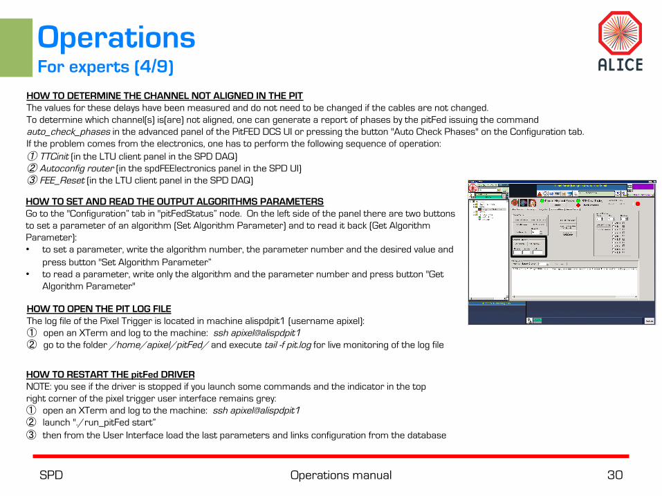
HOW TO SET AND READ THE OUTPUT ALGORITHMS PARAMETERS Go to the "Configuration” tab in "pitFedStatus” node. On the left side of the panel there are two buttons to set a parameter of an algorithm (Set Algorithm Parameter) and to read it back (Get Algorithm Parameter): • to set a parameter, write the algorithm number, the parameter number and the desired value and
press button "Set Algorithm Parameter” • to read a parameter, write only the algorithm and the parameter number and press button "Get
Algorithm Parameter"
HOW TO OPEN THE PIT LOG FILE The log file of the Pixel Trigger is located in machine alispdpit1 (username apixel): ① open an XTerm and log to the machine: ssh apixel@alispdpit1 ② go to the folder /home/apixel/pitFed/ and execute tail -f pit.log for live monitoring of the log file
HOW TO RESTART THE pitFed DRIVER NOTE: you see if the driver is stopped if you launch some commands and the indicator in the top right corner of the pixel trigger user interface remains grey: ① open an XTerm and log to the machine: ssh apixel@alispdpit1 ② launch "./run_pitFed start” ③ then from the User Interface load the last parameters and links configuration from the database
SPD Operations manual 31
Operations For experts (5/9)
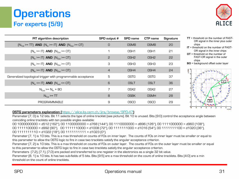
PIT algorithm description SPD output # SPD name CTP name Signature
(NTot >= TT) AND (NIn >= IT) AND (NOut >= OT) 0 0SMB 0SMB 20
(NIn >= IT) AND (NOut >= OT) 1 0SH1 0SH1 21
(NIn >= IT) AND (NOut >= OT) 2 0SH2 0SH2 22
(NIn >= IT) AND (NOut >= OT) 3 0SH3 0SH3 23
(NIn >= IT) AND (NOut >= OT) 4 0SH4 0SH4 24
Generalized topological trigger with programmable acceptance 5 0STG 0STG 37
(Nin <= IT) AND (Nout <= OT) 6 0SLT 0SLT 36
NOut >= NIn + BO 7 0SX2 0SX2 27
NTot >= TT 8 0SBK 0SMH 28
PROGRAMMABLE 9 0SCO 0SCO 29
TT = threshold on the number of FAST-OR signal in the inner plus outer chips
IT = threshold on the number of FAST-OR signal in the inner chips
OT = threshold on the number of FAST-OR signal in the outer chips
BO = background offset outer layer
0STG parameters explanation (https://alice.its.cern.ch/jira/browse/SPD-47) Parameter (7, 0) is 12 bits. Bit 11 selects the type of online tracklet (see picture). Bit 10 is unused. Bits [9:0] control the acceptance angle between coinciding online tracklets with ten possible angles available: 00 1000000000 = d512 (162°), 00 1100000000 = d768 (144°), 00 1110000000 = d896 (126°), 00 1111000000 = d960 (108°), 00 1111100000 = d992 (90°), 00 1111110000 = d1008 (72°), 00 1111111000 = d1016 (54°), 00 1111111100 = d1020 (36°), 00 1111111110 = d1022 (18°), 00 1111111111 = d1023 (0°). Parameter (7, 1) is 10 bits. This is a max threshold on counts of FOs on inner layer. The counts of FOs on inner layer must be smaller or equal to this parameter to allow the 0STG logic to fire in case two tracklets satisfy the angular acceptance criterion. Parameter (7, 2) is 10 bits. This is a max threshold on counts of FOs on outer layer. The counts of FOs on the outer layer must be smaller or equal to this parameter to allow the 0STG logic to fire in case two tracklets satisfy the angular acceptance criterion. Parameters (7,2), (7,1), (7,0) are packed and transferred to one register in the electronics as a single 32 bit value. Parameter (8, 1) is 10 bits. It has two sub-fields of 5 bits. Bits [9:5] are a max threshold on the count of online tracklets. Bits [4:0] are a min threshold on the count of online tracklets.
SPD Operations manual 32
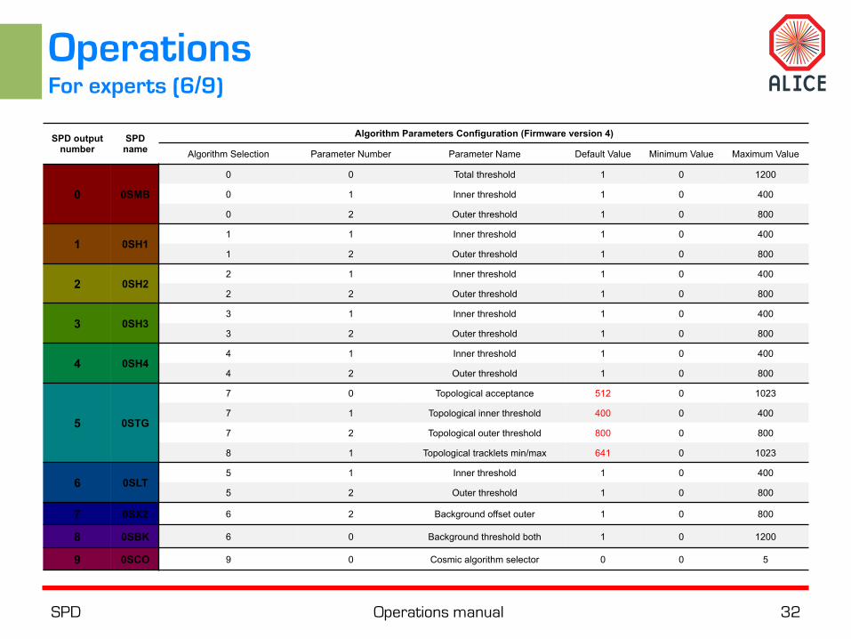
Operations For experts (6/9)
SPD output number
SPD name
Algorithm Parameters Configuration (Firmware version 4)
Algorithm Selection Parameter Number Parameter Name Default Value Minimum Value Maximum Value
0 0SMB
0 0 Total threshold 1 0 1200
0 1 Inner threshold 1 0 400
0 2 Outer threshold 1 0 800
1 0SH1 1 1 Inner threshold 1 0 400
1 2 Outer threshold 1 0 800
2 0SH2 2 1 Inner threshold 1 0 400
2 2 Outer threshold 1 0 800
3 0SH3 3 1 Inner threshold 1 0 400
3 2 Outer threshold 1 0 800
4 0SH4 4 1 Inner threshold 1 0 400
4 2 Outer threshold 1 0 800
5 0STG
7 0 Topological acceptance 512 0 1023
7 1 Topological inner threshold 400 0 400
7 2 Topological outer threshold 800 0 800
8 1 Topological tracklets min/max 641 0 1023
6 0SLT 5 1 Inner threshold 1 0 400
5 2 Outer threshold 1 0 800
7 0SX2 6 2 Background offset outer 1 0 800
8 0SBK 6 0 Background threshold both 1 0 1200
9 0SCO 9 0 Cosmic algorithm selector 0 0 5
SPD Operations manual 33
Operations For experts (7/9)
HOW TO OPERATE THE COOLING PLANT An on-call guide for the cooling system, as prepared during Run1, is available at the following link: http://alice-spd.web.cern.ch/sites/alice-spd.web.cern.ch/files/DetectorOperation/CoolingOnCall-2.pdf. The EN-CV CERN group is responsible for the operation of the plant. Under the supervision of the SPD cooling responsible, they perform the standard checks during the Technical Stop and the unforeseen interventions in case of failure of the system.
HOW TO CHECK THE FLOW WHEN OPENING THE COOLING LOOPS In normal conditions the plant is working and the 10 loops are opened. In the tab “SPD Cooling Status” in the main node of the SPD UI many parameters can be checked for all the 10 loops. Notice that: • If a loop is open we have to move the detector as soon as possible (~1/2 hour) at least in
MCM_ONLY status and keep the module in this status also if it will not be used in data taking (will be excluded from FSM).
• When switching off the detector, it is enough to close the loop and the plant will go in STANBY.
COOLING PLANT FAILURE: FIRST AID KIT In the very rare case you get an alarm, the plant simply stops working and puts itself in the STOP status. In this case no action is allowed from the control room and recovery to normal RUN status is not automatic. An expert MUST check if it is possible to clear the alarm and restart safely the plant. In this case do the following: • Call the TCR (72201) • Tell them that you are calling from the ALICE Control Room and that you need intervention of the DETECTOR COOLING PIQUET for the
SPD (It is very important that you do not omit "DETECTOR" because if you do you get the wrong expert) • Mention that you can be called back to the phone number where you come from (or whatever) because most likely the expert on call will
call you asking some details about the problem, you must mention the kind of alarm you have. • If after a reasonable interval nobody calls, you could call directly the piquet: 162400. DO NOT CALL directly, always call TCR first. • If TCR does not answer for any reason, call directly the Detector Cooling Piquet, 162400 telling you are from ALICE at Point 2 etc. etc.
In the last case (and the piquet will ask you anyway) you MUST call back TCR and announce that you requested the DETECTOR COOLING PIQUET, because of insurance issues and extraordinary intervention invoice.
• Note down in the logbook what happened with all possible details, this information will be very valuable for later debugging of the problem.
SPD Operations manual 34
Operations For experts (8/9)
HOW TO PROGRAM THE ROUTER PERMANENTLY AND TEMPORARLY Permanent programming: The permanent programming of the Router memory is sensibly slower if performed using the new USB based controller system with respect to the old VXI system. the old FED PC containing the VXI cable is still available in CR4 on the floor just under the CAEN main frame. The VXI controllers are still available in the two crates and the cable too. Before to switch on the PC remember to connect the cable to the PC. The following procedure will write in the flash memory, not in the FPGA. To write in the FPGA one has to switch off and on again the crates (after having close the FED services). ① Programming files are store in the folder D:\Labview\router_files; for the permanent programming one needs the file router_fpga_jampof_XXX. ② In the PC, open START à NATIONAL INSTRUMENTS à MEASUREMENT & AUTOMATION à Devices and Interfaces à VXI system à VXIO à MXI-2 Bus 0.
Check if the object VXI0::300::INSTR is present under Frame1 (side A) and 5 (side C). If not, click with the right button on the Frame object, select PROPERTIES. In the tab VME there is the dropdown menu called FRAME from which select the file (Achtung: not MXI2 but FRAME)
③ Still under MEASUREMENT & AUTOMATION go to upper node (should be “VXI System 0”): launch Run VXI resource manager ④ Open the file Router_test_2.vi, available under recent documents; the LABVIEW panel should open ⑤ Select one router: you should zoon out a bit the panel and search the drop down menu called “Router number” in the light gray zone on the right. If working on
the A side, only routers from 0 to 9 are active, while on side C from 10 to 19. To test that the system is working click on the button ReadTempLimit; in case of problem one should receive an error.
⑥ The controller for the actual programming is a below this zone, still in the light grey zone on the right. One should activate ten of the twenty LEDs “Router present” depending on the side and exclude the other. Select the correct file using the browser and select “program” in the small drop down menu.
⑦ If everything is ready, one could launch “RunJamPlayer”: it will give a warning message that can be ignored. When the intervention is finished in the log display should appear a message like ‘Exit code = 0 ... Success’. If the exit code is different from 0 problems occurred. In case of success, one could check from the SPD UI the version of the firmware present in the memory: MANUAL CONFI à ROUTER SETTINGS à PANLE FOR EXPERTS à GENERAL ACCESS TO REGISTERS and read the register 1 selecting one router that has been programmed Temporary programming: This is a much fast way to proceed, but the programming will be lost once the crates are switched off. ① the programming files are stored on the working nodes (alispdwn010 for side A, and alispdwn011 for side C) under D:\spdFED\JamPlayer
\router_jam_files ② the jamsof files are for the soft programming (erased after power cycle of the electronics), the jampof file are for permanent programming (stays after
power cycle of the electronics) ③ from the UI open spdFEElectronics à Manual Config à Router Settings à Panel collection for experts à Program Routers ④ choose the program mode ("Program" for jampof files, "Configure" for jamsof files), the file path and the router to program and launch "Program routers” ⑤ BE CAREFUL!!!! If the jamsof file is used, the programming procedure takes ~10 minutes per router, do not touch anything during this time
D: /spdFed/JamPlayer/router_jam_files/router_fpga_Ver37_P2_sof.jam D: /spdFed/JamPlayer/router_jam_files/router_fpga_jamsof_Ver36_V31.jam
SPD Operations manual 35
Operations For experts (9/9)
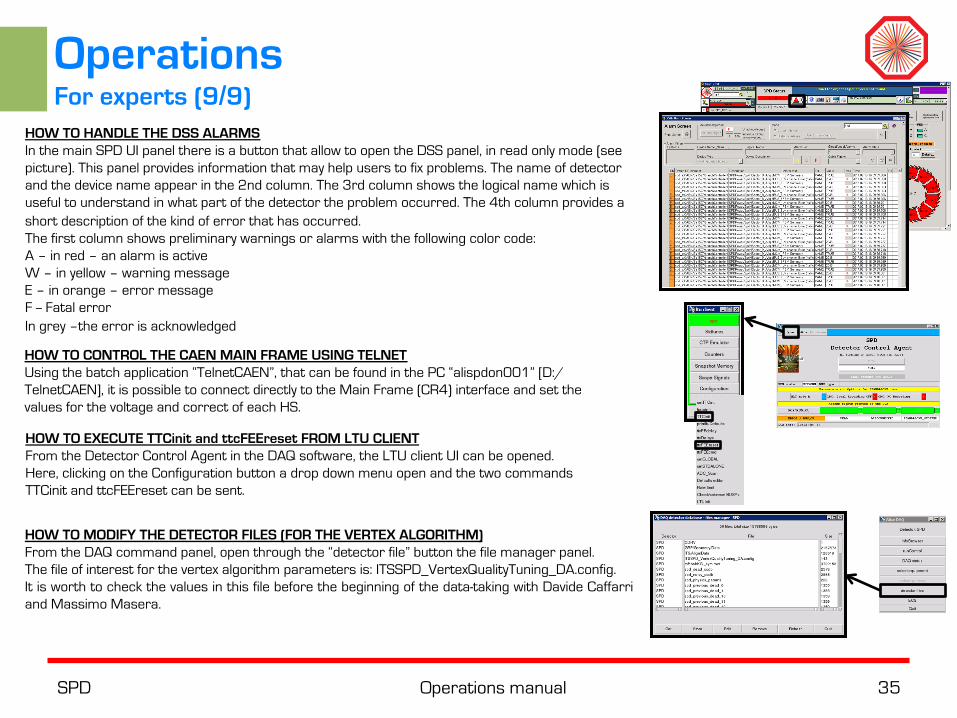
HOW TO HANDLE THE DSS ALARMS In the main SPD UI panel there is a button that allow to open the DSS panel, in read only mode (see picture). This panel provides information that may help users to fix problems. The name of detector and the device name appear in the 2nd column. The 3rd column shows the logical name which is useful to understand in what part of the detector the problem occurred. The 4th column provides a short description of the kind of error that has occurred. The first column shows preliminary warnings or alarms with the following color code: A – in red – an alarm is active W – in yellow – warning message E – in orange – error message F -- Fatal error In grey –the error is acknowledged
HOW TO CONTROL THE CAEN MAIN FRAME USING TELNET Using the batch application “TelnetCAEN”, that can be found in the PC “alispdon001” [D:/TelnetCAEN], it is possible to connect directly to the Main Frame (CR4) interface and set the values for the voltage and correct of each HS.
HOW TO EXECUTE TTCinit and ttcFEEreset FROM LTU CLIENT From the Detector Control Agent in the DAQ software, the LTU client UI can be opened. Here, clicking on the Configuration button a drop down menu open and the two commands TTCinit and ttcFEEreset can be sent.
HOW TO MODIFY THE DETECTOR FILES (FOR THE VERTEX ALGORITHM) From the DAQ command panel, open through the “detector file” button the file manager panel. The file of interest for the vertex algorithm parameters is: ITSSPD_VertexQualityTuning_DA.config. It is worth to check the values in this file before the beginning of the data-taking with Davide Caffarri and Massimo Masera.
SPD Operations manual 36
Data monitoring and Calibration Overview
The SPD is a digital detector, therefore the main check is to ensure that the data format are: § consistent within itself à data format error § consistent within the event à lack of correlation between data coming from both layers,
tracklets inefficiency The SPD is also a trigger detector (PIT system), therefore further checks are related to: § the rate of the trigger for the output included in the global trigger logic à presence of noisy
chip or pixel § consistency of the trigger information stored in the data à Hits vs FastOr correlation Many instruments, working online and offline, have been developed to check the quality of the data: o Online
ü Amore agents (SPDQAshifter and SPDHits) ü Further online monitoring (noisy trigger, SPD-MOOD, Reference Data Displayer)
o Offline ü Raw data analysis ü QA offline
To make the detector work in the proper way and to solve potential inconsistency in the data discovered through the online/offline monitoring, calibration procedures have been developed: o Preliminary procedures
ü Timing alignment ü Chip configuration (Minimum Threshold Scan, Uniformity Scan, Mean Threshold, FastOr
efficiency and uniformity, General DAC Scan) o Offline procedures
ü OCDB re-production
The SPD on-call shifter will deal with a minimum part of these instruments (Amore agents, noisy trigger monitoring) with the goal to spot problems as soon as possible during the data taking in order to be able to take immediate actions. The rest of the instruments are used by the experts.
q Data Format and Errors [slide 37] q Amore agents [slide 40]
ü SPDHits ü SPDQAShifter
q Trigger monitoring [slide 42] q For experts [slide 43]
ü Further monitoring tools ü Raw data analysis ü QA offline ü Preliminary calibrations ü Offline calibrations
SPD Operations manual 37
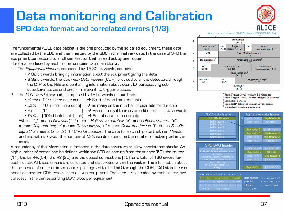
Data monitoring and Calibration SPD data format and correlated errors (1/3)
SPD data frame SPD DAQ header
half stave 0
half stave data frame chip header 0 0
1
m
pixel hit 0 pixel hit 1 pixel hit 2
pixel hit n-1 chip trailer 0 chip header 1 chip trailer 1 chip header 2 pixel hit 0
pixel hit 1 pixel hit 2
pixel hit n-2 pixel hit n-1 fill word chip trailer 2
chip header3 pixel hit 0 pixel hit 1 pixel hit 2
pixel hit n-1 chip trailer 9
chip header chip addr event number hs hs = half stave 0 to 5
0 1 2 3 4 5 6 7 8 9 10 11 12 13 14 15
1 0
hit addr row address 0 X 1 X = not used, set to 0 pixel hit fill word 1 1 X X X X X X X X X X X X X X chip trailer 0 0 chip hit count f e
e = error, f = fastOr
SPD DAQ header
SP
D data form
at A
. Kluge, M
. Krivda, 2009 11 12
block length
half stave 1 half stave 2 half stave 3 half stave 4 half stave 5
L1 trigger info, bunch crossing numb. orbit number
block&a(ribut.,&par0cip.&subdetectors status&and&errors,&mini&event&ID&
trigger&classes&low&ROI&low,&trigger&classes&high&
ROI&high
The fundamental ALICE data packet is the one produced by the so called equipment. these data are collected by the LDC and then merged by the GDC in the final raw data. In the case of SPD the equipment correspond to a full semi-sector that is read out by one router. The data produced by each router contains two main blocks: 1. The Equipment Header, composed by 15 32-bit words, contains:
• 7 32-bit words bringing information about the equipment giving the data • 8 32-bit words, the Common Data Header (CDH): provided to all the detectors through
the CTP to the FEE and containing information about event ID, participating sub-detectors, status and error, mini-event ID, trigger classes.
2. The Data words (payload), composed by 16-bit words of four kinds: • Header [01ss seee eeee cccc] à Start of data from one chip • Data [10_r rrrr rrrro oooo] à as many as the number of pixel hits for the chip • Fill [11__ ____ ____ ____] à Present only if there is an odd number of data words • Trailer [00fb hhhh hhhh hhhh] à End of data from one chip
Where: “_” means Not used, “s” means Half stave number, “e” means Event counter, “c” means Chip number, “r” means Row address, “o” means Column address, “f” means FastOr signal, “b” means Error bit, “h” Chip hit counter. The data for each chip start with an Header and end with a Trailer; the number of Data words depend on the number of active pixel in the event.
A redundancy of the information is foreseen in the data structure to allow consistency checks. An high number of errors can be defined within the SPD as coming from the trigger (50), the router (11), the LinkRx (54), the HS (30) and the optical connections (15) for a total of 160 errors for each router. All these errors are collected and elaborated within the router. The information about the presence of an error in the data is propagated to the DAQ through the CDH; DAQ stop the run once reached ten CDH errors from a given equipment. These errors, decoded by each router, are collected in the corresponding DQM plots per equipment.
https://cds.cern.ch/record/984071/files/ALICE-INT-2002-010.pdf
SPD Operations manual 38
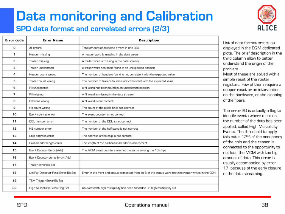
Error code Error Name Description
0 All errors Total amount of detected errors in one DDL
1 Header missing A header word is missing in the data stream
2 Trailer missing A trailer word is missing in the data stream
3 Trailer unexpected A trailer word has been found in an unexpected position
4 Header count wrong The number of headers found is not consistent with the expected value
5 Trailer count wrong The number of trailers found is not consistent with the expected value
6 Fill unexpected A fill word has been found in an unexpected position
7 Fill missing A fill word is missing in the data stream
8 Fill word wrong A fill word is not correct
9 Hit count wrong The count of the pixels hit is not correct
10 Event counter error The event counter is not correct
11 DDL number error The number of the DDL is not correct
12 HS number error The number of the half-stave is not correct
13 Chip address error The address of the chip is not correct
14 Calib header length error The length of the calibration header is not correct
15 Event Counter Error (Adv) The MCM event counters are not the same among the 10 chips
16 Event Counter Jump Error (Adv) --
17 Trailer Error Bit Set --
18 LinkRx/Detector Fatal Error Bit Set Error in the front-end status, extracted from bit 6 of the status word that the router writes in the CDH
19 TSM Trigger Error Bit Set --
20 High Multiplicity Event Flag Set An event with high multiplicity has been recorded -> high multiplicity cut
List of data format errors as displayed in the DQM dedicated plots. The brief description in the third column allow to better understand the origin of the problem. Most of these are solved with a simple reset of the router registers. Few of them require a deeper reset or an intervention on the hardware, as the cleaning of the fibers. The error 20 is actually a flag to identify events where a cut on the number of the data has been applied, called High Multiplicity Events. The threshold to apply this cut is 12% of the occupancy of the chip and the reason is connected to the opportunity to not load the MCM with too big amount of data. This error is usually accompanied by error 17, because of the early closure of the data streaming.
Data monitoring and Calibration SPD data format and correlated errors (2/3)
SPD Operations manual 39
Data monitoring and Calibration SPD data format and correlated errors (3/3)
A dedicated module, called Error Handler, has been implemented in the router firmware to allow a deeper encoding of the information about the error. A complete documentation is available here: http://aliweb.cern.ch/SPD/DetectorOperation/RunInfo/ErrorHandler.html. We have already shown how to activate this module in the electronics and how to send a query. Here a list of errors and suggestion action to solve the problem:
TTCRX and QPLL link error The TTC link is an optical link that comes from the TTC-LTU splitter to each Router. If this is not ready, the TTCRX chip and the Router do not work properly. à Check the status of the TTC optical link and the QPLL lock status
Trigger errors from CTP Not consistent trigger signals are received by the TTCRX chip of the Routers. This may be due to different reasons: invalid trigger pattern sent to the back-end electronics, L0-L1 delay not properly set, LTU not well configured, TTCRX chip not well configured (as a consequence of a TTCInit command not sent to the chip). à Reset TTCRX chip on all the Routers + send ttcInit and ttcFEEReset command from LTU client
Timeout BCNT reset Timeout for the synchronization between the HS clock phase and the LHC BC reset. It occurs when the ttcFEEreset command is received by the Router but the BCreset signal is not correctly received by the TTCRX chip. As a consequence, the Reset clock phase is not propagated from the Router. à Reset TTCRX chip on all the Routers + send ttcInit and ttcFEEReset command from LTU client
Trigger_errors from master trigger control FSM in router The trigger signals that come from the TTC are consistent, but some signals are lost inside the Routers; as a consequence, trigger signals do not propagate properly to the LRx and to the detector. à Router, LRx and DPI reset
DAQ Link not ready The DAQ Optical Link (DDL) is not ready for the data acquisition. à Inform the DAQ expert Error optical link of half-staves This error indicates which half-stave optical link is missing as a consequence of a problem present on an optical fiber or because the half-stave is switched off. à
Check if the HS have to be ON or exclude it from the Router Error optical connection Many errors are taken into account in this flag: errors in the Agilent component of the LinkRX connection, sequences CAV-DAV not coherent, First, Last, Clear bit events
not coherent, undefined command decoded by the PILOT2003 deserializer, MCM event counter number not coherent. à Check the quality of the optical fiber transmission Error_HS_LinkRx_0 ... 5 It takes into account the internal errors coming from the LRx or the detector and happens when the half-stave is not properly configured. à Router, LRx and DPI and
Data reset + HS configuration Timeout HS The timeout is set during the data acquisition when a half-stave does not transmit any data in 1000 μs (max time defined inside the spdFED in TimeoutReadyEvent register). It
normally occurs when the multi-event buffer is not properly set on the MCM. à Check the value of the Multi Event Buffer on the DPI manual control Data error format This error is set during the data acquisition and takes into account all the errors present in the data stream before the sending operation to the DAQ. à Router, LRx and DPI
reset FastOr missing in data The Fast-OR bit is not present in the data stream. The module checks if at least one hit is present inside the chip matrix and if the Fast-OR bit is present in the trailer field.
If the Fast-OR bit is not there, the error is generated. à Set the proper delay between the Fast-Or and the L1 signals inside the LinkRx Error longer busy Error generated when the Router receive a valid TTC FEE Reset from CTP (during TTCInit procedure) but the QPLL is still not ready and TTC FEE Reset is not received properly
from HS, implying that the clock phase are not alignments together. à TTCFEEReset during router busy Set an Error flag if the Busy time coming from SPD is more long than a time threshold (set in the router at the areg=h0c, default value is 500 msec). à Inform
the Trigger Support High multiplicity There is an event with high multiplicity (>10% chip occupancy). The readout of the event is cut to guarantee the overall readout time of 256 us. This is a warning, not a real
error. à Any action is needed
How these error can be distinguished is explicitly described in the document already cited at the beginning.
SPD Operations manual 40
Data monitoring and Calibration Amore agent: SPDHits
① Missing Fast-OR per BCmod4 [top] The “Missing FO/BCmod4” plots show, separately for each BC%4, the relative number of “missing FO” counts per chip. A “missing FO” is counted if, for that chip, a pixel hit is registered without a corresponding FO signal. The X axis (from 0 to 1199) shows the chip-key index (= iEQ*60+iHS*10 + iChip) while the Y axis shows the relative fraction of missing FO counts. The overall FO efficiency is also displayed for each BC%4 on top of each plot.
② Hits per event per DDL [middle left] This plot shows the average number of pixel hits per event per DDL (or Equipment). The X axis shows the Equipment number (20 routers from 0 to 19), while the Y axis show the average number of hits per event.
③ Data Format Errors [middle] Similarly to the “Error Codes” plot in the SPDQAShifter agent, this plot shows the number of data format errors per DDL per error type. The X axis shows the DDL number, while the Y axis shows the error code. In this agent, the error names are also explicated on the labels.
④ Noisy Pixel [middle right] This panel is displayed if at least 1 noisy pixel is identified by the QA framework. Up to 5 pixels identified as “noisy” can be shown in the agent. A pixel is identified as “noisy” if it yields a “hit” in more than 3% of events. The Equipment, HS and chip, along with the row and column of the pixels identified as noisy are printed in the agent.
⑤ Fast-OR maps [bottom] Two histograms show the maps for the Fast-OR bit in the inner (left) and outer (right) layer. The Y axis shows the SPD sector number "SX" and the Half Stave (HS) number, while the X axis shows the chip number in online notation. Here, chips that are masked in the OCDB are not filled (shown as empty bins) in the histograms.
Two amoreAgents produce monitoring plots for the SPD in the logbook and needed to judge the quality of the run: -- SPDQAshifter: available to the DQM shifter (TWiki: https://twiki.cern.ch/twiki/bin/viewauth/ALICE/EVESPD) -- SPDHits: stored in the Logbook for each run Some information are duplicated in the output of the two agents, granting more reliability.
SPD Operations manual 41
Data monitoring and Calibration Amore agent: SPDQAshifter
① Data Format Errors [top left] The Data format QA "Error Codes" plot shows the number of data format errors per DDL (or equipment) per error type: the X axis shows the number of the DDL (20 routers from 0 to 19), while the Y axis shows the error code. The decoded errors are 19, from 1 to 20; row corresponding to error type 0 shows the sum of all the errors occurred in that equipment. The entries represent the number of occurrence of the corresponding error.
② Hits vs FO Correlation (MEB problem) [bottom left] This histogram shows presence of loss of correlation between the hits and the Fast-Or information in the stream of the data; in the past this has been used to spot presence of problem in the operation of the Multi-Event-Buffer (MEB) in some chip. The notation is compact in this case: The Y axis shows the chip number in online notation, while the X axis shows Sector "SX" and Stave number in a compact way, with stave number ranging from 0 to 5.
③ Hit maps [top right] Two histograms show the map of the hits per chip in the two layers (inner and outer); note that there are 10 chips per HS for a total of 20 chips per Stave. The plots are filled with the number of pixel hit per chip. The X axis shows the chip number in online notation, while the Y axis shows the SPD sector number "SX" and the Half Stave (HS) number: the Half-Staves belonging to the inner layer are always 0 and 1, whereas the ones belonging to the outer layer are always 2,3,4,5.
④ Fast-OR maps [bottom right] Similarly to the “FastOr Maps” in the SPDHits agent, these plots show the Fast-OR bits per chip in both inner (left) and outer (right) layer. As in the previous case: the Y axis shows the SPD sector number "SX" and the Half Stave (HS) number, while the X axis shows the chip number in online notation. Conversely to the SPDQAShifter agent, chips that are masked in the OCDB are filled in the histograms.
AMORE interface The DQM panel can be opened from every PC in the ARC:
amore –d TRI –m Expert
SPD Operations manual 42
Data monitoring and Calibration Trigger monitoring
The rate of the ten PIT outputs depends on the activity of the chips and also the presence of a single noisy pixel can make these outputs noisy. There are many ways to check the rates of the outputs and the origin of the noise: • From the internet browser, the page alitri.cern.ch, accessible
only within the P2 network, in the Monitoring section, has a CTP counter system that allow to show online the trend of the PIT outputs.
• In the PIT DCS, under the pitFED node, a tab Monitor Counters reports for all the ten outputs: increments, instantaneous rate, average rate, total counts.
• For each run, in the Logbook, under DQM Info tab in the folder TRI, a lot of trigger related plots are stored. Two specific sets of plots are interesting for us: L0 input rates and class ratios.
Once observed an anomaly in the rates, one could search the cause looking at presence of noisy pixels or of a noisy chips (this second case could happen if the chip parameters for the FastOR line are not well set): • In the output of the Amore agent SPDHits, a special plot appear in case of presence of a noisy pixel (pixel
yielding a “hit” in more than 3% of events). • Presence of a noisy chip can be seen quite easily looking at the FastOr maps produced by the SPDHits Amore
agent (where the mask of noisy chips is applied). • In the PIT DCS, still under the pitFED node, two different panel allow to search for a noisy chip in the PIT.
ü In the Configuration tab, there is a section called Status Checks where it is possible to start and stop a counter and show in the log screen only the chips that have count larger then a choose threshold (this has to be properly selected depending on the circumstance).
ü A similar system is present in the tab Link Settings where the same procedure can be applied and the counts are shown for each chips in a selected HS.
The procedures to mask a noisy pixel or to exclude a chip from the mask have been already described.
SPD Operations manual 43
Data monitoring and Calibration For expert: Further monitoring tools (1/5)
SPD MOOD SPD-MOOD is a monitoring program intended for expert use in the SPD team, running both online and on offline raw data files. Documentation can be found at the following link: https://alice-spd.web.cern.ch/Monitoring/SPDmood.html. It runs on Linux (developed at SLC4), and needs ROOT, and DATE in the online case. Note: during 2015 and 2016 it has never been used. From the Run2 period, in accordance with the DAQ, the test software must be installed on DAQ machine, in particular on ‘aldaqdqm05’ machine. An rpm has to be produced and asked to the DAQ to be added to the list of program to be automatically installed.
REFERENCE DISPLAYER The goal of this software can be argued looking at the function behind buttons in the main panel: Copy Reference Data Button is visible only if program compiled for P2. Copies reference data files (using perl scripts) from the LDCs to
the monitoring machine where this program runs. Display Reference Data Displays reference data files (without analyzing them). In most cases this means that a hit-map is displayed. May
read from local files as well as from grid (see above how to do that). Analyze Reference Data Displays reference data files, and analyze them (perform the same tasks as the DAs, and display the results).
May read from local files as well as from grid (see above how to do that). Run DA Offline Button is visible only if program not compiled for P2. Gives the possibility to run DA on local raw data file in offline mode (if
offline DA version is available) using perl script. Copy DCS Config Output Button is visible only if program compiled for P2. Copies DCS Config Output files (using perl scripts) from the
LDCs to the monitoring machine where this program runs. Display DCS Config Output Displays DCS Config Output files. (These are the files generated when running a DA that sends output for the
Detector Configuration DB.) Further documentation is available here: https://alice-spd.web.cern.ch/Monitoring/SPDmood/Instructions.html and https://alice-spd.web.cern.ch/Monitoring/Calibration/ReferenceDisplayer.html.
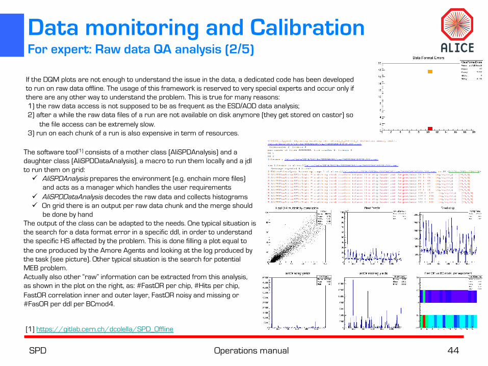
SPD Operations manual 44
Data monitoring and Calibration For expert: Raw data QA analysis (2/5)
The software tool[1] consists of a mother class (AliSPDAnalysis) and a daughter class (AliSPDDataAnalysis), a macro to run them locally and a jdl to run them on grid:
ü AliSPDAnalysis prepares the environment (e.g. enchain more files) and acts as a manager which handles the user requirements
ü AliSPDDataAnalysis decodes the raw data and collects histograms ü On grid there is an output per raw data chunk and the merge should
be done by hand The output of the class can be adapted to the needs. One typical situation is the search for a data format error in a specific ddl, in order to understand the specific HS affected by the problem. This is done filling a plot equal to the one produced by the Amore Agents and looking at the log produced by the task (see picture). Other typical situation is the search for potential MEB problem. Actually also other “raw” information can be extracted from this analysis, as shown in the plot on the right, as: #FastOR per chip, #Hits per chip, FastOR correlation inner and outer layer, FastOR noisy and missing or #FasOR per ddl per BCmod4.
[1] https://gitlab.cern.ch/dcolella/SPD_Offline
If the DQM plots are not enough to understand the issue in the data, a dedicated code has been developed to run on raw data offline. The usage of this framework is reserved to very special experts and occur only if there are any other way to understand the problem. This is true for many reasons: 1) the raw data access is not supposed to be as frequent as the ESD/AOD data analysis; 2) after a while the raw data files of a run are not available on disk anymore (they get stored on castor) so
the file access can be extremely slow. 3) run on each chunk of a run is also expensive in term of resources.
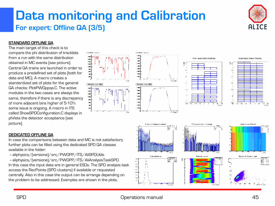
SPD Operations manual 45
Data monitoring and Calibration For expert: Offline QA (3/5)
STANDARD OFFLINE QA The main target of this check is to compare the phi distribution of tracklets from a run with the same distribution obtained in MC events (see picture). Central QA trains are launched in order to produce a predefined set of plots (both for data and MC). A macro creates a standardized set of plots for the general QA checks: PlotPWGppqa.C. The active modules in the two cases are always the same, therefore if there is any discrepancy of more adjacent bins higher of 5-10% some issue is ongoing. A macro in ITS called ShowSPDConfiguration.C displays in phi/eta the detector acceptance (see picture).
DEDICATED OFFLINE QA In case the comparisons between data and MC is not satisfactory further plots can be filled using the dedicated SPD QA classes available in the folder: -- aliphysics/(versione)/src/PWGPP/ITS/AliSPDUtils -- aliphysics/(versione)/src/PWGPP/ITS/AliAnalysisTaskSPD. In this case the input data are in general ESDs. The SPD analysis task access the RecPoints (SPD clusters) if available or requested centrally. Also in this case the output can be arrange depending on the problem to be addressed. Examples are shown in the plots.
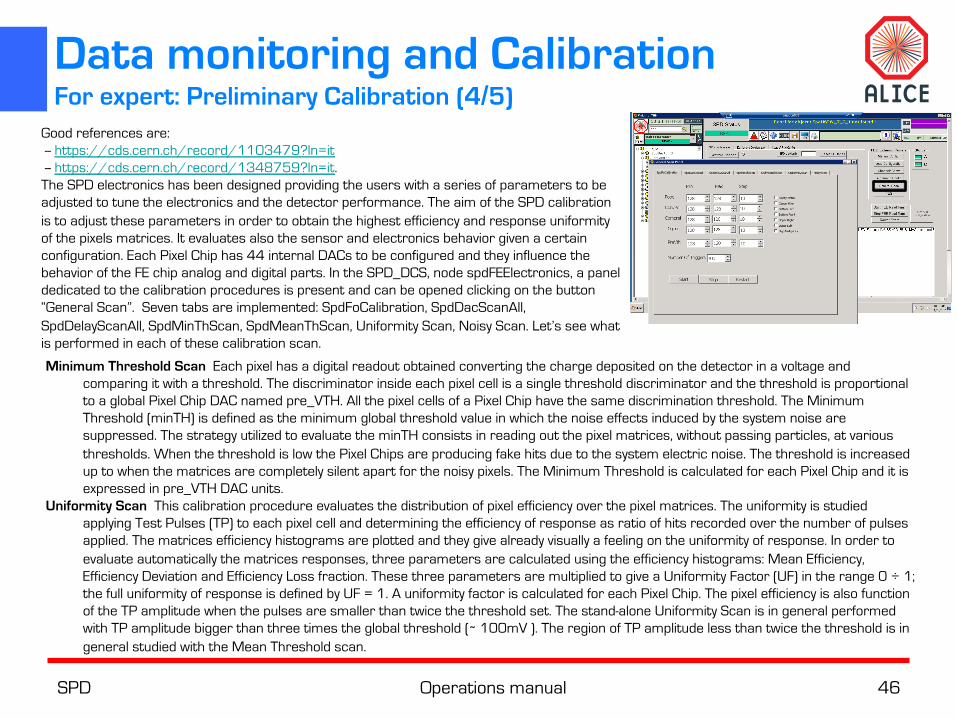
SPD Operations manual 46
Data monitoring and Calibration For expert: Preliminary Calibration (4/5)
Minimum Threshold Scan Each pixel has a digital readout obtained converting the charge deposited on the detector in a voltage and comparing it with a threshold. The discriminator inside each pixel cell is a single threshold discriminator and the threshold is proportional to a global Pixel Chip DAC named pre_VTH. All the pixel cells of a Pixel Chip have the same discrimination threshold. The Minimum Threshold (minTH) is defined as the minimum global threshold value in which the noise effects induced by the system noise are suppressed. The strategy utilized to evaluate the minTH consists in reading out the pixel matrices, without passing particles, at various thresholds. When the threshold is low the Pixel Chips are producing fake hits due to the system electric noise. The threshold is increased up to when the matrices are completely silent apart for the noisy pixels. The Minimum Threshold is calculated for each Pixel Chip and it is expressed in pre_VTH DAC units.
Uniformity Scan This calibration procedure evaluates the distribution of pixel efficiency over the pixel matrices. The uniformity is studied applying Test Pulses (TP) to each pixel cell and determining the efficiency of response as ratio of hits recorded over the number of pulses applied. The matrices efficiency histograms are plotted and they give already visually a feeling on the uniformity of response. In order to evaluate automatically the matrices responses, three parameters are calculated using the efficiency histograms: Mean Efficiency, Efficiency Deviation and Efficiency Loss fraction. These three parameters are multiplied to give a Uniformity Factor (UF) in the range 0 ÷ 1; the full uniformity of response is defined by UF = 1. A uniformity factor is calculated for each Pixel Chip. The pixel efficiency is also function of the TP amplitude when the pulses are smaller than twice the threshold set. The stand-alone Uniformity Scan is in general performed with TP amplitude bigger than three times the global threshold (∼ 100mV ). The region of TP amplitude less than twice the threshold is in general studied with the Mean Threshold scan.
Good references are: -- https://cds.cern.ch/record/1103479?ln=it -- https://cds.cern.ch/record/1348759?ln=it. The SPD electronics has been designed providing the users with a series of parameters to be adjusted to tune the electronics and the detector performance. The aim of the SPD calibration is to adjust these parameters in order to obtain the highest efficiency and response uniformity of the pixels matrices. It evaluates also the sensor and electronics behavior given a certain configuration. Each Pixel Chip has 44 internal DACs to be configured and they influence the behavior of the FE chip analog and digital parts. In the SPD_DCS, node spdFEElectronics, a panel dedicated to the calibration procedures is present and can be opened clicking on the button “General Scan”. Seven tabs are implemented: SpdFoCalibration, SpdDacScanAll, SpdDelayScanAll, SpdMinThScan, SpdMeanThScan, Uniformity Scan, Noisy Scan. Let’s see what is performed in each of these calibration scan.
SPD Operations manual 47
Data monitoring and Calibration For expert: Preliminary Calibration (4/5)
Mean Threshold Scan The Mean Threshold (meanTH) is a parameter establishing the conversion factor between the charge deposited on the detector volume and the corresponding threshold DAC value. Different sets of supply and reference voltages require a new evaluation of the conversion factor. Moreover the change over time of the meanTH indicates detector and electronics aging effects. The method used to calculate the meanTH gives also information on the electronics noise associated to each pixel cell. The Mean Threshold is evaluated applying to each pixel a series of TPs with various amplitudes. For each pixel an efficiency curve (named S-curve, from its typical shape) function of the TP amplitude is plotted. It is defined as Mean Threshold for each pixel the amplitude of TP to which the pixel has an efficiency of 50%. The Pixel Chip meanTH is the mean value of the pixels meanTH distribution. The meanTH is evaluated repeating a series of Uniformity Scans with various TP amplitudes.
Noise and Dead pixels The aging, the radiation effects and the mechanical stress can increment the number of not functioning channels. The survey and identification of noise and dead channels is a detector calibration procedure. Noise pixels can be consequence of either malfunctioning pixel cells in the FE chips or bad sensor diodes. Dead pixels are in general either consequence of missing bump-bonding be- tween the sensors and the FE electronics or defects in the FE chip readout channels. New dead pixels can appear due to mechanical stress or by radiation effects. The noisy pixel identification is performed during the various calibration procedures as well as during dedicated procedures. In the specific noise scan few millions of triggers are sent to the detectors without any stimulation (neither particles nor TPs). The pixels producing hits are defined noisy. The dead pixels are identified using particles produced by the interactions during the experiment data taking. The data are collected until the average multiplicity is above a certain value defined by the operator. The pixels with either low (< 20%) or null efficiency are defined as dead.
FastOR efficiency and uniformity The FastOR signal is generated, asynchronously, by each Pixel Chip, whenever a pixel is fired on the matrix. The Fast-OR circuitry operation is controlled by four Pixel Chip internal DACs influencing the Fast-OR response in term of uniformity along the pixel matrices and the FastOR efficiency. The Fast-OR calibration studies these parameters and it defines the best DACs settings to obtain the higher efficiency and uniformity. The Fast-OR uniformity and efficiency are studied applying to a pixel at a time a given number of TPs and reading back the number or Fast-OR produced. Efficiency maps are produced associating to each pixel the corresponding number of Fast-OR counted. The histograms produced have the same structure of the Uniformity Scan histograms. Hence, the same method are used to evaluate Fast-OR uniformity and efficiency. The operations described are repeated several times modifying the DACs values in order to reach the full uniformity of response and efficiency.
Generic DAC scan The generic DAC scan is used to study the FE electronics and detector performances as function of a Pixel Chips DACs. The methods described in the previous sections are focalized to extract a defined set of operational parameters whereas the DAC scan is completely generic; it is used to evaluate the system performance and tightly adjust the detector operation point. The DAC scan is performed applying a sequence of trigger to the detector under test, using either TPs or particles, while varying the references generated by the Ana- log Pilot and/or a specific DAC in the Pixel Chips. The readout data are used to produce average multiplicity and efficiency histograms function of the DAC values.
SPD Operations manual 48
Data monitoring and Calibration For expert: Preliminary Calibration (4/5)
To be finished
Delay Scan The pixel readout electronics has a programmable delay line to adjust the L1 latency respect to the particle arrival. This delay can be operated acting on two Pixel Chip internal DACs: delay control and misc control. The former increases the delay of 200 ns for DAC unit whereas misc control can delays the incoming L1 of 100 ns. The L1 latency is guaranteed to be ~6 µs at the Router card level depending on the ALICE trigger partition used. However the effective arrival to the Pixel Chips depends on the command serialization/de-serialization time and to the optical fibers length. One clock cycle (100 ns) L1 jitter can also be introduced during the off-detector electronics reset phase. A calibration procedure has been designed to find the appropriate delay: Delay Scan. This scan modifies the values on the two DACs involved while a series of triggers is sent to the detector. Using the collected data, a multiplicity plot shows the multiplicity distribution as function of the delay set. This plot spots the right delay as a pick of multiplicity above the background.
Fast-OR line The 1200 Fast-OR bits are transmitted every 100 ns to the Routers by the MCM without any further processing in the read-out cell. Two electronic registers align the SPD clock to the LHC clock: the BClock, which provides 25 ns shifts, and the FineDelay1, which can fine-tune the alignment down to a level of a tenth of nanosecond.
Hits line When a particle hits the detector, the signal is synchronized to the 10 MHz internal
clock; inside the delay lines the pulse is delayed by an integer number of clock cycles and the duration of it can be programmed with the Delay_control register, settable by a dedicated DAC of the front-end chip. The strobe window can also be delayed of 100 ns inside the chip; this is done changing the Misc_setting register of the front-end chip. The signal is stored in the delay line waiting for the L1 trigger coming from the ALICE Central Trigger Processor. The L1 trigger signal is sent in parallel to the MCMs; there the trigger is translated into a strobe signal that is applied to all front-end chips. The duration of the strobe window is programmable and can be changed with the Strobe_length register of the MCM. Changing these three parameteres, the strobe readout window can be timed with the presence at the output of the delay lines of the pulse generated by a particle inside the detector.
SPD Operations manual 49
Data monitoring and Calibration For expert: Offline Calibration (5/5)
The SPD calibration objects to be handles are: SPDDead: HSs not included in the DAQ
• Produced by the SPD PHYS DA run-by-run • The HS in the DAQ are written in the raw data according to the HSs included in the “channel view” of the SPD DCS panel • Object used, both in data and MC, to remove the HS dead from the reconstruction process • Previously the SPD PHYS DA was killed before providing the calibration objects à the object had to be produced manually • If one/more chip/s or one/more HS/s are not working correctly they have to be masked à the reconstruction has to be done
again • The misbehavior of such chips or HSs is spotted clearly in the tracklet phi distribution
SPDNoisy: pixel considered noisy (= firing more than 5% of the events) • Produced by the SPD PHYS DA run-by-run • Object used, both in data and MC, to remove the noisy pixels from the reconstruction process • Previously the SPD PHYS DA was killed before providing the calibration objects à the object had to be produced manually
• Noisy pixels are always available in the DQM plots for experts SPDSparseDead: dead pixels inside the active HSs
• Produced by SPD operator every few LHC periods • The comparison data/MC of the tracklet phi distribution shows limited regions in phi (basically they represent the borders of
the HS) where data reduction is shown • The increase of this dead pixels is few per mille per LHC period so they are pretty stable per year • Object used only in MC
The interface class that manages the calibration objects within the CDB classes is AliITSOnlineCalibrationSPDhandler. In the next slide we will see how to reproduce or modify these OCDB files.
SPD Operations manual 50
REPRODUCE AN OCDB FILE IN CASE OF FAILURE OF THE DA 1) Look at the neighboring physics run of the problematic sun (yyy) and choose one that has
the same HS configuration (xxx) 2) Produce the new OCDB file copying the one of the chosen neighbor run
• Connect to Alien and open Aliroot AliITSOnlineCalibrationSPDhandler *h = new AliITSOnlineCalibrationSPDhandler() h->ReadDeadFromDB(xxx,"alien://folder=/alice/data/2015/OCDB"); h->WriteDeadToDB(179571,179571,"local:///opt/ocdb");
where /home/colella/ocdb is the destination folderNotice the 3 / after local! 3) Verify that the produced file is equal to the original one
• Open Aliroot and initialize the handler AliITSOnlineCalibrationSPDhandler *h = new AliITSOnlineCalibrationSPDhandler() h->ReadDeadFromDB(xxx,"alien://folder=/alice/data/2013/OCDB"); AliITSOnlineCalibrationSPDhandler *hloc = new AliITSOnlineCalibrationSPDhandler() hloc->ReadDeadFromDB(179571,"local:///opt/ocdb");
• Perform a check h->PrintDiffInDead(hloc)
the output has to be "1200 coherent chips" with 0 mismatch 4) Open a ticket on JIRA and assign it to Chiara Zampolli: the new file has to stored in the
folder ITS/Calib/SPDDead 5) Check that the file stored on Alien is correct
• Open Aliroot and initialize the two handlers AliITSOnlineCalibrationSPDhandler *h = new AliITSOnlineCalibrationSPDhandler() h->ReadDeadFromDB(179571,"alien://folder=/alice/data/2013/OCDB"); AliITSOnlineCalibrationSPDhandler *hloc = new AliITSOnlineCalibrationSPDhandler() hloc->ReadDeadFromDB(179571,"local:///opt/ocdb");
• Effettuare il confronto h->PrintDiffInDead(hloc)
MASK NOISY PIXEL AliITSOnlineCalibrationSPDhandler *h = new AliITSOnlineCalibrationSPDhandler() h->SetNoisyPixel(8,5,8,31,88) h->WriteNoisyToDB(184780,184780,"local:///opt/ocdb") MASK CHIP AliITSOnlineCalibrationSPDhandler *h = new AliITSOnlineCalibrationSPDhandler(); h->ReadDeadFromDB(179603,"alien://folder=/alice/data/2012/OCDB"); h->SetDeadChip(13,1,0); h->WriteDeadToDB(179603,179603,"local:///opt/ocdb"); MASK HALF-STAVE AliITSOnlineCalibrationSPDhandler *h = new AliITSOnlineCalibrationSPDhandler(); h->ReadDeadFromDB(179638,"alien://folder=/alice/data/2012/OCDB"); for(Int_t ic =0; ic<10; ic++) h->SetDeadChip(18,5,ic); h->WriteDeadToDB(179638,179638,"local:///opt/ocdb"); CHECK THE NOISY PIXELS Read the noisy pixels present in the local file and on alien Local file: AliITSOnlineCalibrationSPDhandler *h = new AliITSOnlineCalibrationSPDhandler(); h->ReadNoisyFromDB(179571,"local:///opt/ocdb"); h->PrintNoisy(); File onAlien: AliITSOnlineCalibrationSPDhandler *h = new AliITSOnlineCalibrationSPDhandler(); h->ReadNoisyFromDB(179571,"alien://folder=/alice/data/2012/OCDB"); h->PrintNoisy();
Data monitoring and Calibration For expert: Offline Calibration (5/5)
SPD Operations manual 51
Useful links
SPD [1] Main website: http://alice-spd.web.cern.ch [2] SPD operational manual: https://drive.google.com/file/d/0B5nG1xNTPzEJODk4bkFyZW5QWUk/view?usp=sharing [3] SPD on-call instructions: https://drive.google.com/file/d/0B5nG1xNTPzEJdVNWZ3JMbFNKME0/view?usp=sharing [4] Private logbook: https://drive.google.com/open?id=1ALu-dcIrcyfGPN53uaNbNRP2ru5-BEOUUHDIyVKlJ3s [5] Run2 data-taking : https://drive.google.com/open?id=12Q6mYsKPeWOuYrmEnpA1ej6WtaFH2RaG9jVJyB9MIHc [6] JIRA project: https://alice.its.cern.ch/jira/projects/SPD/summary [7] GitLab Offline project: https://gitlab.cern.ch/dcolella/SPD_Offline
ARC@P2 [8] Logbook: https://alice-logbook.cern.ch/logbook/date_online.php?p_cont=lc&p_cvm=Compact&pcf_ctc=,,20&p_cpn=1 [9] ECS display: https://aldaqweb.cern.ch/sd/ [10] DCS monitoring: http://alicedcs.web.cern.ch/AliceDCS/monitoring/main.aspx [11] LHC page 1: https://op-webtools.web.cern.ch/vistar/vistars.php?usr=LHC1 [12] ALICE Run Coordination webpage: http://alice-collaboration.web.cern.ch/run_coordination/run/index.html [13] ALICE data taking description (Federico R. 28 Nov 2014 Junior’s day): https://indico.cern.ch/event/347071/session/0/contribution/72/material/slides/2.pdf