Embed Size (px)
DESCRIPTION
Xcell Journal 日本語版 79 & 80 合併号では、ザイリンクスが 4 年の歳月を費やして開発した次の10年の「All Programmable」デバイスに対応する Vivado Design Suiteや業界初のヘテロジニアス3D FPGAである Virtex-7 H580T の記事を掲載しています。
Citation preview
「All Programmable」デバイスに対応するVivado Design Suite
フォーマル検証を使用した FPGA IP コアの ハードウェア /ソフトウェア協調検証
Kintex-7 FPGA を使用した19nm フラッシュ PCIe SSDの設計
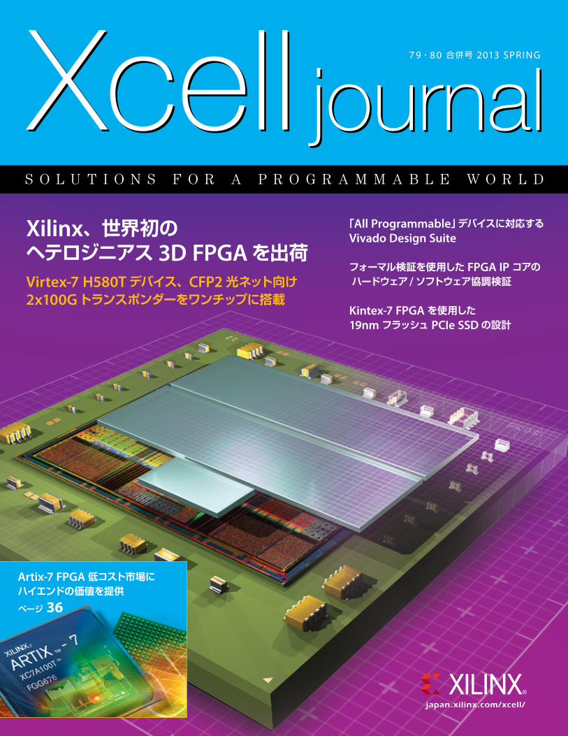
Xilinx、世界初のヘテロジニアス 3D FPGAを出荷Virtex-7 H580Tデバイス、CFP2光ネット向け2x100Gトランスポンダーをワンチップに搭載
Artix-7 FPGA 低コスト市場にハイエンドの価値を提供
S O L U T I O N S F O R A P R O G R A M M A B L E W O R L D
Xcell journalXcell journal7 9・8 0 合併号 2013 SPRING
ページ 36
¥12,800(税込13,440)
¥12,000(税込12,600)
¥19,500(税込20,475)
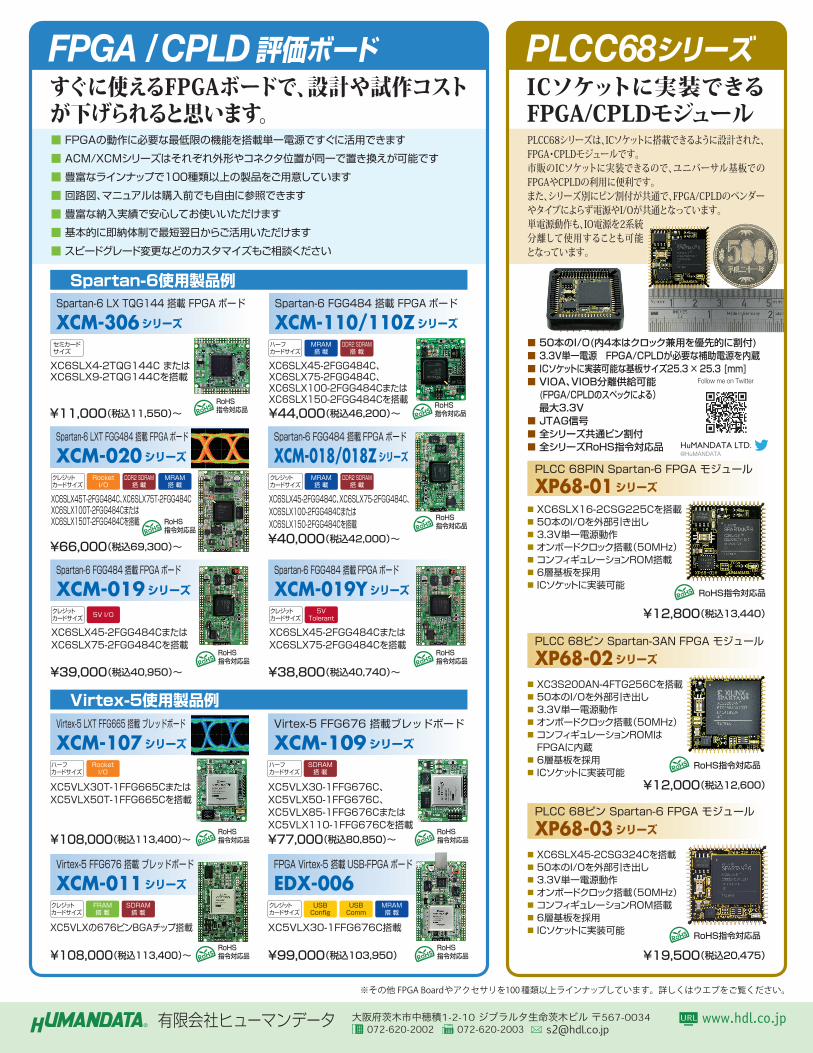
FPGA / CPLD評価ボード PLCC68
■ FPGAの動作に必要な最低限の機能を搭載単一電源ですぐに活用できます
■ ACM/XCMシリーズはそれぞれ外形やコネクタ位置が同一で置き換えが可能です
■ 豊富なラインナップで100種類以上の製品をご用意しています
■ 回路図、マニュアルは購入前でも自由に参照できます
■ 豊富な納入実績で安心してお使いいただけます
■ 基本的に即納体制で最短翌日からご活用いただけます
■ スピードグレード変更などのカスタマイズもご相談ください
Spartan-6使用製品例
XP68-01シリーズPLCC 68PIN Spartan-6 FPGA モジュール
※その他 FPGA Boardやアクセサリを100種類以上ラインナップしています。詳しくはウエブをご覧ください。
シリーズすぐに使えるFPGAボードで、設計や試作コストが下げられると思います。
ICソケットに実装できるFPGA/CPLDモジュールPLCC68シリーズは、ICソケットに搭載できるように設計された、FPGA・CPLDモジュールです。市販のICソケットに実装できるので、ユニバーサル基板でのFPGAやCPLDの利用に便利です。また、シリーズ別にピン割付が共通で、FPGA/CPLDのベンダーやタイプによらず電源やI/Oが共通となっています。単電源動作も、IO電源を2系統分離して使用することも可能となっています。
■ 50本のI/O(内4本はクロック兼用を優先的に割付)■ 3.3V単一電源 FPGA/CPLDが必要な補助電源を内蔵■ ICソケットに実装可能な基板サイズ25.3 × 25.3 [mm]■ VIOA、VIOB分離供給可能 (FPGA/CPLDのスペックによる) 最大3.3V■ JTAG信号■ 全シリーズ共通ピン割付■ 全シリーズRoHS指令対応品
■ XC6SLX16-2CSG225Cを搭載■ 50本のI/Oを外部引き出し■ 3.3V単一電源動作■ オンボードクロック搭載(50MHz)■ コンフィギュレーションROM搭載■ 6層基板を採用■ ICソケットに実装可能
RoHS指令対応品
RoHS指令対応品
XP68-02シリーズPLCC 68ピン Spartan-3AN FPGA モジュール
■ XC3S200AN-4FTG256Cを搭載■ 50本のI/Oを外部引き出し■ 3.3V単一電源動作■ オンボードクロック搭載(50MHz)■ コンフィギュレーションROMはFPGAに内蔵
■ 6層基板を採用■ ICソケットに実装可能
RoHS指令対応品
XP68-03シリーズPLCC 68ピン Spartan-6 FPGA モジュール
■ XC6SLX45-2CSG324Cを搭載■ 50本のI/Oを外部引き出し■ 3.3V単一電源動作■ オンボードクロック搭載(50MHz)■ コンフィギュレーションROM搭載■ 6層基板を採用■ ICソケットに実装可能
セミカードサイズ
RoHS指令対応品¥11,000(税込11,550)~
XCM-306シリーズ
Spartan-6 LX TQG144 搭載 FPGAボード
XC6SLX4-2TQG144C または XC6SLX9-2TQG144Cを搭載
ハーフカードサイズ
DDR2 SDRAM搭 載
MRAM搭 載
RoHS指令対応品¥44,000(税込46,200)~
XCM-110/110Zシリーズ
Spartan-6 FGG484 搭載 FPGAボード
XC6SLX45-2FGG484C、XC6SLX75-2FGG484C、XC6SLX100-2FGG484CまたはXC6SLX150-2FGG484Cを搭載
DDR2 SDRAM搭 載
RoHS指令対応品
クレジットカードサイズ
RocketI/O
MRAM搭 載
¥66,000(税込69,300)~
XC6SLX45T-2FGG484C、XC6SLX75T-2FGG484CXC6SLX100T-2FGG484CまたはXC6SLX150T-2FGG484Cを搭載
XCM-020シリーズ
Spartan-6 LXT FGG484 搭載 FPGAボード
USBConfig
FRAM搭 載
ハーフカードサイズ
SDRAM搭 載
クレジットカードサイズ
USBComm
クレジットカードサイズ
Virtex-5使用製品例
XCM-011シリーズ
Virtex-5 FFG676 搭載 ブレッドボード
XC5VLXの676ピンBGAチップ搭載
¥108,000(税込113,400)~
EDX-006FPGA Virtex-5 搭載USB-FPGAボード
XC5VLX30-1FFG676C搭載
¥99,000(税込103,950)
XCM-109シリーズ
Virtex-5 FFG676 搭載ブレッドボード
XC5VLX30-1FFG676C、XC5VLX50-1FFG676C、XC5VLX85-1FFG676CまたはXC5VLX110-1FFG676Cを搭載¥77,000(税込80,850)~
ハーフカードサイズ
RocketI/O
MRAM搭 載
XCM-107シリーズ
Virtex-5 LXT FFG665 搭載 ブレッドボード
XC5VLX30T-1FFG665CまたはXC5VLX50T-1FFG665Cを搭載
¥108,000(税込113,400)~
SDRAM搭 載
RoHS指令対応品
RoHS指令対応品
RoHS指令対応品
RoHS指令対応品
クレジットカードサイズ
RoHS指令対応品
¥40,000(税込42,000)~
XC6SLX45-2FGG484C、XC6SLX75-2FGG484C、XC6SLX100-2FGG484CまたはXC6SLX150-2FGG484Cを搭載
XCM-018/018Zシリーズ
Spartan-6 FGG484 搭載 FPGAボード
MRAM搭 載
DDR2 SDRAM搭 載
5VTolerant5V I/O クレジット
カードサイズ
RoHS指令対応品
¥38,800(税込40,740)~
XC6SLX45-2FGG484CまたはXC6SLX75-2FGG484Cを搭載
XCM-019Yシリーズ
Spartan-6 FGG484 搭載 FPGAボード
クレジットカードサイズ
RoHS指令対応品
¥39,000(税込40,950)~
XC6SLX45-2FGG484CまたはXC6SLX75-2FGG484Cを搭載
XCM-019シリーズ
Spartan-6 FGG484 搭載 FPGAボード
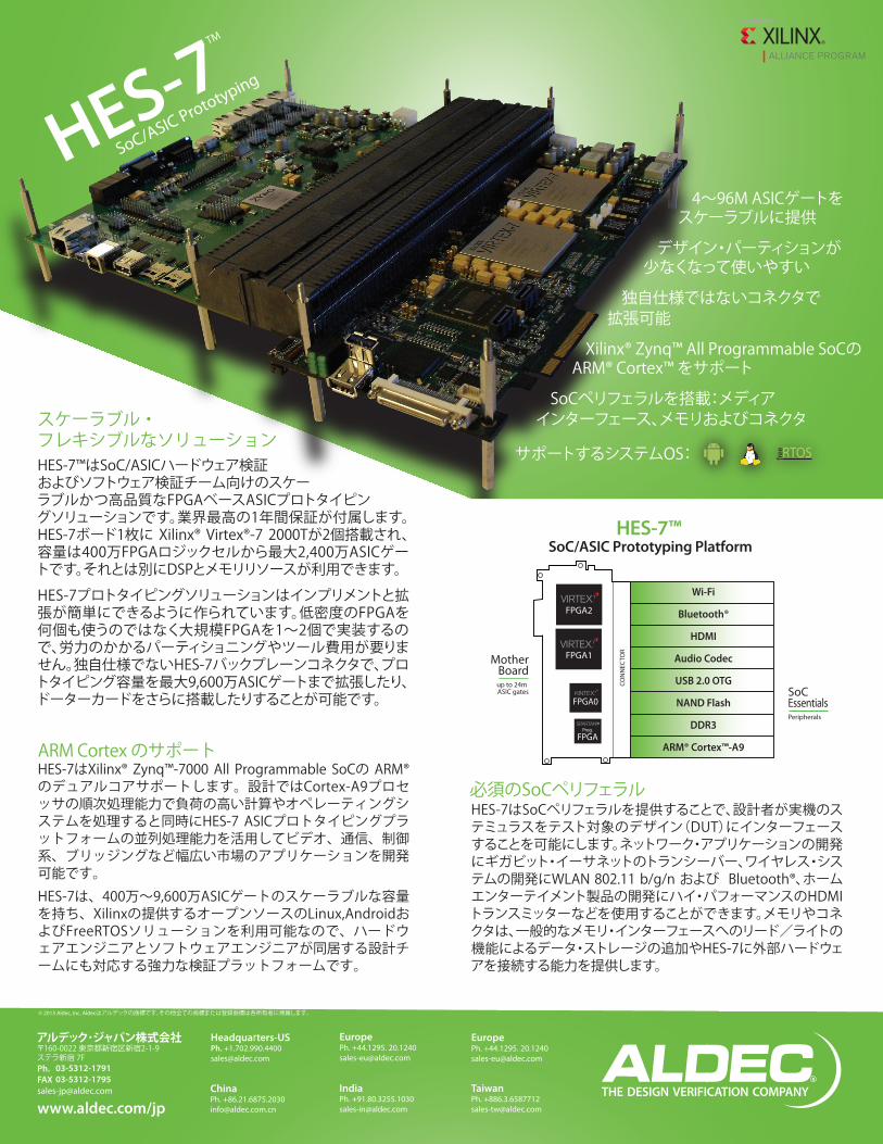
HES-7™はSoC/ASICハードウェア検証およびソフトウェア検証チーム向けのスケーラブルかつ高品質なFPGAベースASICプロトタイピングソリューションです。業界最高の1年間保証が付属します。HES-7ボード1枚に Xilinx® Virtex®-7 2000Tが2個搭載され、容量は400万FPGAロジックセルから最大2,400万ASICゲートです。それとは別にDSPとメモリリソースが利用できます。
HES-7プロトタイピングソリューションはインプリメントと拡張が簡単にできるように作られています。低密度のFPGAを何個も使うのではなく大規模FPGAを1~2個で実装するので、労力のかかるパーティショニングやツール費用が要りません。独自仕様でないHES-7バックプレーンコネクタで、プロトタイピング容量を最大9,600万ASICゲートまで拡張したり、ドーターカードをさらに搭載したりすることが可能です。
HES-7 SoC/ASIC Prototyping
スケーラブル・フレキシブルなソリューション
THE DESIGN VERIFICATION COMPANYR
必須のSoCペリフェラル HES-7はSoCペリフェラルを提供することで、設計者が実機のステミュラスをテスト対象のデザイン(DUT)にインターフェースすることを可能にします。ネットワーク・アプリケーションの開発にギガビット・イーサネットのトランシーバー、ワイヤレス・システムの開発にWLAN 802.11 b/g/n および Bluetooth®、ホームエンターテイメント製品の開発にハイ・パフォーマンスのHDMIトランスミッターなどを使用することができます。メモリやコネクタは、一般的なメモリ・インターフェースへのリード/ライトの機能によるデータ・ストレージの追加やHES-7に外部ハードウェアを接続する能力を提供します。
4~96M ASICゲートをスケーラブルに提供
デザイン・パーティションが少なくなって使いやすい
独自仕様ではないコネクタで拡張可能
Xilinx® Zynq™ All Programmable SoCのARM® Cortex™ をサポート
SoCペリフェラルを搭載:メディアインターフェース、メモリおよびコネクタ
サポートするシステムOS:
HES-7™ SoC/ASIC Prototyping Platform
MotherBoardup to 24m ASIC gates
FPGA2
FPGA1
FPGA0
Prog.
FPGA
CON
NEC
TOR
SoCEssentialsPeripherals
Wi-Fi
Bluetooth®
HDMI
Audio Codec
USB 2.0 OTG
NAND Flash
DDR3
ARM® Cortex™-A9
freeRTOS
ARM Cortex のサポートHES-7はXilinx® Zynq™-7000 All Programmable SoCの ARM® のデュアルコアサポートします。設計ではCortex-A9プロセッサの順次処理能力で負荷の高い計算やオペレーティングシステムを処理すると同時にHES-7 ASICプロトタイピングプラットフォームの並列処理能力を活用してビデオ、通信、制御系、ブリッジングなど幅広い市場のアプリケーションを開発可能です。HES-7は、400万~9,600万ASICゲートのスケーラブルな容量を持ち、Xilinxの提供するオープンソースのLinux,AndroidおよびFreeRTOSソリューションを利用可能なので、ハードウェアエンジニアとソフトウェアエンジニアが同居する設計チームにも対応する強力な検証プラットフォームです。
© 2013 Aldec, Inc. Aldecはアルデックの商標です。その他全ての商標または登録商標は各所有者に帰属します。
Headquarters-USPh. [email protected]
EuropePh. +44.1295. 20.1240 [email protected]
EuropePh. +44.1295. [email protected]
ChinaPh. [email protected]
TaiwanPh. [email protected]
IndiaPh. [email protected]
アルデック・ジャパン株式会社〒160-0022 東京都新宿区新宿2-1-9 ステラ新宿 7FPh. [email protected]
www.aldec.com/jp
TM
member
03-5312-179103-5312-1795
L E T T E R F R O M T H E P U B L I S H E R
プログラマブル デバイスのルネサンスへようこそ時が経つのは早いものです。最近私はザイリンクス入社 4 周年を祝いました。私は 40nm 6 シリー
ズ FPGA と 28nm 7 シリーズ デバイス、この 2 つの新世代シリコンの市場投入という困難な作業に参加する中で、素晴らしい経験をさせていただきました。私は今、ザイリンクスが 世界初の FPGA である XC2064 を 1985 年に発表して以来、プログラマブル ロジックの歴史でおそらく最も刺激的で革新的な瞬間に立ち会えることを誇りに思っています。
2011 年ザイリンクスは、世界初の 28nm プロセス シリコンの販売を開始しましたが、これに引き続き Zynq™ -7000 All Programmable SoC と Virtex®-7 2000T FPGA という 2 つの革命的なテクノロジを発表しました。
ここ 2、3 年の Xcell Journal をお読みの方は、この 2 つの優れたデバイスについてよくご存じのことと思います。Zynq-7000 AP SoC は、デュアルコアの ARM® Cortex™ -A9 MPCore プロセッサとプログラマブル ロジックを同一デバイス上に統合した製品であり、プログラマブル ロジックからではなくプロセッサ コアからブートします。このデバイスは、従来の FPGA 設計者にはシステムレベルのインテグレーションに新たな展望をもたらし、大規模なユーザー基盤を形成しているソフトウェア技術者にはプログラマブル ロジックの新たな世界を開くものです。それは留まるところを知らない潜在能力を秘めています。
このデバイスに熱烈な興味を持っているのは私だけではありません。Zynq-7000 AP SoC はEE Times 誌と EDN 誌の編集者と読者の投票により、UBM Electronics 社主催の ACE アワードで SoC ( システム オン チップ ) 製品最優秀賞を受賞しています (http://www.eetimes.com/electronics-news/4370156/Xilinx-Zynq-7000-receives-product-of-the-year-ACE-award を参照 )。
さらに、個人的には Virtex-7 2000T も ACE アワードのデジタル IC 最優秀製品のカテゴリでファイナリストに選ばれ、これは Zynq-7000 AP SoC に劣らず素晴らしい技術的偉業と言えるでしょう。Virtex-7 2000T は、ザイリンクスの 3D スタックド シリコン インターコネクト (SSI) テクノロジを初めて採用した市販の FPGA であり、4 個の 28nm プログラマブル ロジック ダイ ( スライスと呼ばれる ) を並べてパッシブ シリコン インターポーザー上にインプリメントしています。Virtex-7 2000T は、ダイを積み重ねることで、ワンチップのデバイスとしては世界で最も多くのトランジスタを搭載し、史上最高の集積度を備えたプログラマブル ロジック デバイスを実現しました。
SSI テクノロジは、ムーアの法則を超えるスピードで高集積度 IC をカスタマーに提供するだけでなく、さまざまなタイプのダイをワンチップ上に統合した製品を実現し、ユーザーのイノベーションを加速する、新しいインテグレーションの可能性を開きます。たとえば、ザイリンクスは、SSI テクノロジによって作られた Virtex-7 HT ファミリ デバイスを発表しました。このファミリの各メンバーは、トランシーバー スライスとプログラマブル ロジック スライスをワンチップ上にインプリメントしています。Virtex-7 HT ファミリにより、有線通信機器メーカーは、新しい 100Gbps およびそれ以上の帯域幅規格に準拠する機器を開発できます。Virtex-7 HT ファミリで最大の集積度を持つ Virtex-7 H870T を使用すれば、最先端の通信規格に準拠した最大 400Gbps で動作する機器の開発も可能です。
さらに素晴らしいことに、現在ザイリンクスは新しい Vivado™ Design Suite の販売を開始しています (カバー ストーリー、ページ 12-17 を参照)。5 年前にザイリンクスが開発に着手した Vivado は、ISE® Design Suite よりもランタイムがはるかに高速化しただけでなく、オープン規格と ( 高合成を含む ) 最新の EDA テクノロジを採用してゼロから設計されたツールであり、7 シリーズ デバイスおよび今後数世代にわたる FPGA の生産性を飛躍的に向上させます。
新しい 7 シリーズ デバイスと Vivado Design Suite にぜひご注目してください。昨年 6 月にサンフランシスコにて開催された Design Automation Conference (www.dac.
com) でこれら7シリーズ製品とデザインツールは、非常に注目されたものでした。今後の7シリーズとVivado Design Suite の活躍に期待がもたれます。
Mike Santarini 発行人
Xcell journal発行人 Mike Santarini [email protected] +1-408-626-5981
編集 Jacqueline Damian
アートディレクター Scott Blair
デザイン/制作 Teie, Gelwicks & Associates
日本語版統括 秋山 一雄 [email protected]
制作進行
日本語版 制作・広告
周藤 智子[email protected]
有限会社エイ・シー・シー
Xcell Journal 日本語版 79・80 合併号
2013 年 2 月 28 日発行
Xilinx, Inc2100 Logic DriveSan Jose, CA 95124-3400
ザイリンクス株式会社〒 141-0032東京都品川区大崎 1-2-2アートヴィレッジ大崎セントラルタワー 4F
Ⓒ 2013 Xilinx, Inc. All Right Reserved.
XILINX や、Xcell のロゴ、その他本書に記載の商標は、米国およびその他各国の Xilinx 社の登録商標です。
本書は、米国 Xilinx, Inc. が発行する英文季刊誌を、ザイリンクス株式会社が日本語に翻訳して発行したものです。
米国 Xilinx, Inc. およびザイリンクス株式会社は、本書に記載されたデータの使用に起因する第三者の特許権、他の権利、損害における一切の責任を負いません。
本書の一部または全部の無断転載、複写は、著作権法に基づき固く禁じます。
ほかすべての名前は、各社の登録商標または商標です。
ウェブセミナー
ニーズに合わせたプログラムを各種取り揃えて好評配信中!!
FPGA入門編
FPGA活用編
開発ツール編
FPGA/SoC概要編
FPGAをこれから始める方にFPGAの全体概要を解説した入門編と、ものづくりにチャレンジする経営者、技術管理者の方へなぜ今FPGA /CPLDなのかをご説明します。
ザイリンクスFPGAを使った最先端デザインの設計手法や、さまざまなアプリケーション設計に求められるデザイン チャレンジに対するソリューションをご紹介・解説します。
プログラマブルデバイスであるFPGAの設計には開発ツールがキーになります。ザイリンクスが提供するユーザー フレンドリーな開発ツールの特徴や使い方、先端設計メソドロジについて解説します。
FPGAの世界トップシェアを誇るザイリンクスが提案するソリューションや、ザイリンクスの最先端FPGA の詳細を解説します。
30分で判る! FPGA入門
Zynq-7000 All Programmable SoC での C コードから コプロセッシング アクセラレーターZynq-7000 All Programmable SoC での C コードから コプロセッシング アクセラレーター
AMBA AXI4 テクニカルセミナー
次世代FPGA設計手法セミナー PlanAhead デザイン解析ツール~ 第1部、 第2部、 第3部、 デモ ~
7 シリーズ ターゲット デザイン プラットフォーム
ザイリンクス シリアル デザイン ソリューション
15分で判る! FPGA採用理由
7 シリーズ FPGA で消費電力を大幅に削減
製品の差別化を実現する開発ツール:ISE Design Suite
http://japan.xilinx.com/webseminar/セミナー内容の詳細/ご視聴は今すぐこちらから
All Programmable FPGA および SoC、3D IC の世界的なリーディング プロバイダーのザイリンクスが提供するプログラマブル ロジックからプログラマブル システム インテグレーションのさまざまな機能と活用方法をご紹介します。コストを抑え、最大のパフォーマンスを実現するための最新情報を手に入れてください。
New!!New!!
Web Seminar
新セミナー登場
エクステンシブル プロセッシング プラットフォーム Zynq-7000 ファミリのご紹介
Zynq-7000 EPP アーキテクチャとエコシステム
28nm ザイリンクス 7 シリーズ FPGA のアジャイル ミックスド シグナル テクノロジ
VIEWPOINTS
Letter From the Publisher
プログラマブル デバイスのルネサンスへようこそ… 2
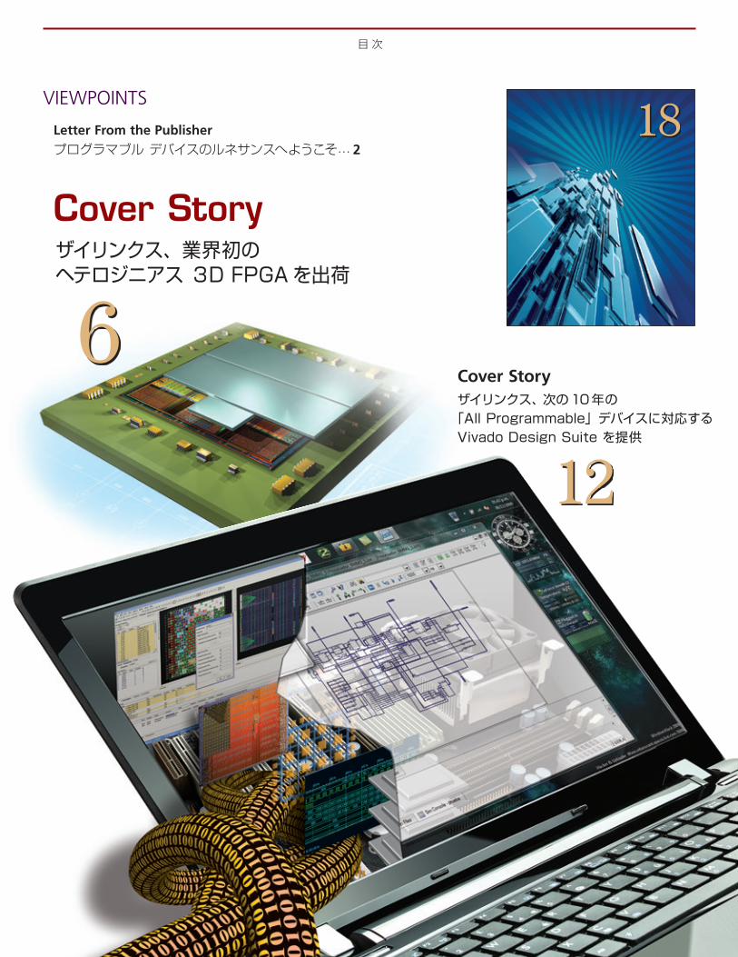
Cover Storyザイリンクス、次の 10 年の
「All Programmable」デバイスに対応する Vivado Design Suite を提供
目 次
Cover Storyザイリンクス、業界初のヘテロジニアス 3D FPGA を出荷
6
18
12
XCELLENCE BY DESIGN APPLICATION FEATURES
THE XILINX XPERIENCE FEATURES
Xcellence in Communications
高レベル合成ツールによるパケット エンジン デザインの最適化… 18
Xcellence in Solid-State Storage
Kintex-7 FPGA を使用した19nm フラッシュ PCIe SSD の設計… 23
Xcellence in Distributed Computing
FPGA による分散型コンピューティングの高速化… 28
Product Feature
ザイリンクス、低コスト市場にハイエンドの価値を提供する Artix-7 FPGA を出荷… 36
7 9 ・ 8 0 合 併 号
広告索引有限会社ヒューマンデータ………表 2アルデック・ジャパン株式会社 ……1
Xpert Opinion
FPGA デザイン内での CORDIC アルゴリズムの使用方法… 42
Xplanation: FPGA101
フォーマル検証を使用した FPGA IP コアのハードウェア/ ソフトウェア協調検証… 47
Xplanation: FPGA 101
FPGA エンジニア ガイド : ADC と DAC の使用法… 53
Xpert Opinion
FPGA の応用 クラウドを加速化… 58
58Excellence in Magazine & Journal Writing
2010, 2011Excellence in Magazine & Journal Design and Layout
2010, 2011, 2012
28
36
53
COVER STORY
ザイリンクス、業界初のヘテロジニアス 3D FPGA を出荷 :Virtex-7 H580T
Xilinx Introduces First Heterogeneous 3D FPGA:
6 Xcell Journal 79・80 合併号
C O V E R S T O R Y
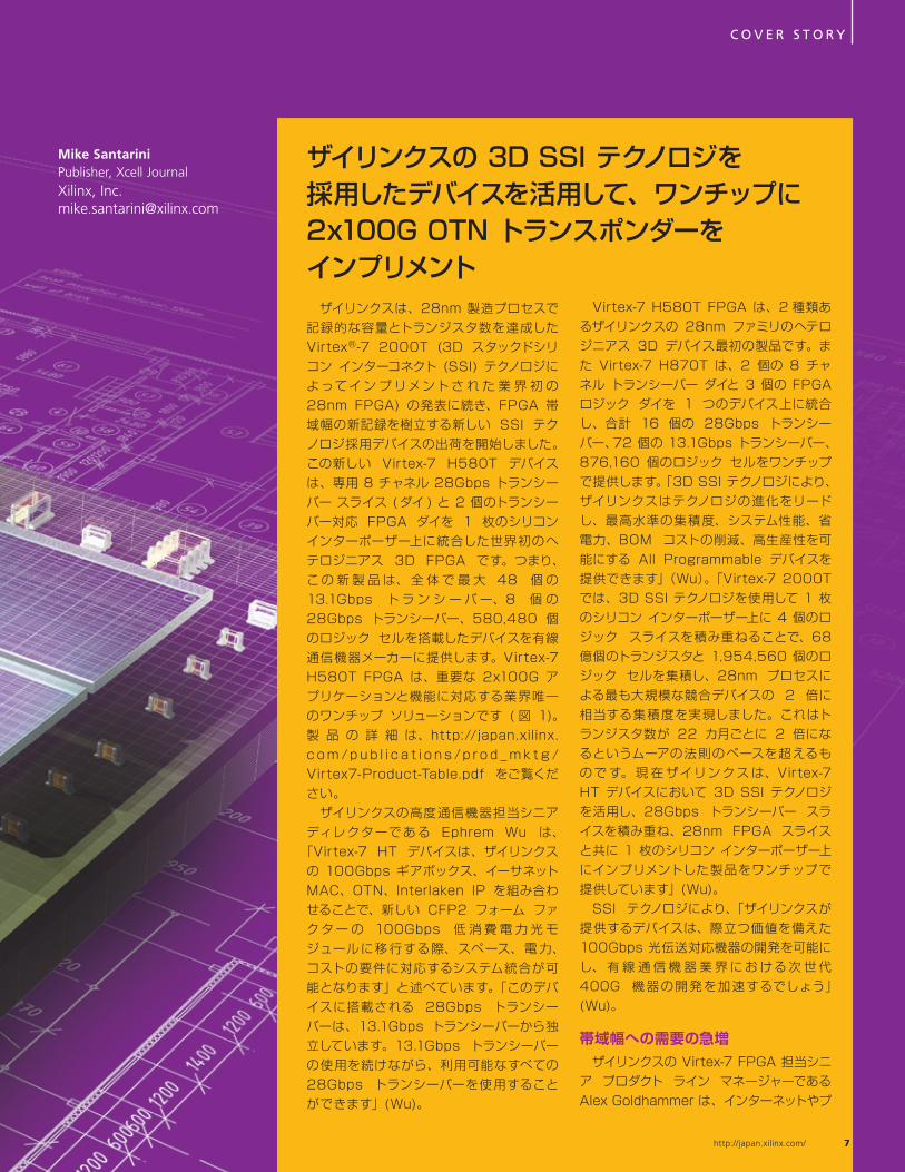
Mike SantariniPublisher, Xcell Journal
Xilinx, [email protected]
ザイリンクスの 3D SSI テクノロジを採用したデバイスを活用して、ワンチップに 2x100G OTN トランスポンダーをインプリメント ザイリンクスは、28nm 製造プロセスで記録的な容量とトランジスタ数を達成した Virtex®-7 2000T (3D スタックドシリコン インターコネクト (SSI) テクノロジによってイ ン プ リメント さ れ た 業 界 初 の 28nm FPGA) の発表に続き、FPGA 帯域幅の新記録を樹立する新しい SSI テクノロジ採用デバイスの出荷を開始しました。この新しい Virtex-7 H580T デバイスは、専用 8 チャネル 28Gbps トランシーバー スライス ( ダイ ) と 2 個のトランシーバー対応 FPGA ダイを 1 枚のシリコン インターポーザー上に統合した世界初のヘテロジニアス 3D FPGA です。つまり、この 新 製 品 は、 全 体 で 最 大 48 個 の 13.1Gbps ト ラ ン シ ー バ ー、8 個 の 28Gbps トランシーバー、580,480 個のロジック セルを搭載したデバイスを有線通信機器メーカーに提供します。Virtex-7 H580T FPGA は、重要な 2x100G アプリケーションと機能に対応する業界唯一のワンチップ ソリューションです ( 図 1)。製 品 の 詳 細 は、http://japan.xilinx.c o m /p u b l i c a t i o ns /p r o d _ m k t g /Virtex7-Product-Table.pdf をご覧ください。 ザイリンクスの高度通信機器担当シニア ディレクターである Ephrem Wu は、
「Virtex-7 HT デバイスは、ザイリンクスの 100Gbps ギアボックス、イーサネット MAC、OTN、Interlaken IP を組み合わせることで、新しい CFP2 フォーム ファクター の 100Gbps 低 消 費 電 力 光 モジュールに移行する際、スペース、電 力、コストの要件に対応するシステム統合が可能となります」と述べています。「このデバイスに搭載される 28Gbps トランシーバーは、13.1Gbps トランシーバーから独立しています。13.1Gbps トランシーバーの使用を続けながら、利用可能なすべての 28Gbps トランシーバーを使用することができます」(Wu)。
Virtex-7 H580T FPGA は、2 種類あるザイリンクスの 28nm ファミリのヘテロジニアス 3D デバイス最初の製品です。また Virtex-7 H870T は、2 個の 8 チャネル トランシーバー ダイと 3 個の FPGA ロジック ダイを 1 つのデバイス上に統合し、合計 16 個の 28Gbps トランシーバー、72 個の 13.1Gbps トランシーバー、876,160 個のロジック セルをワンチップで提供します。「3D SSI テクノロジにより、ザイリンクスはテクノロジの進化をリードし、最高水準の集積度、システム性能、省電力、BOM コストの削減、高生産性を可能にする All Programmable デバイスを提供できます」(Wu)。「Virtex-7 2000T では、3D SSI テクノロジを使用して 1 枚のシリコン インターポーザー上に 4 個のロジック スライスを積み重ねることで、68 億個のトランジスタと 1,954,560 個のロジック セルを集積し、28nm プロセスによる最も大規模な競合デバイスの 2 倍に相当する集積度を実現しました。これはトランジスタ数が 22 カ月ごとに 2 倍になるというムーアの法則のペースを超えるもので す。 現 在 ザイリンクス は、Virtex-7 HT デバイスにおいて 3D SSI テクノロジを活用し、28Gbps トランシーバー スライスを積み重ね、28nm FPGA スライスと共に 1 枚のシリコン インターポーザー上にインプリメントした製品をワンチップで提供しています」(Wu)。 SSI テクノロジにより、「ザイリンクスが提供するデバイスは、際立つ価値を備えた 100Gbps 光伝送対応機器の開発を可能にし、 有 線 通 信 機 器 業 界 に お ける次 世 代 400G 機器の開発を加速するでしょう」(Wu)。
帯域幅への需要の急増 ザイリンクスの Virtex-7 FPGA 担当シニア プロダクト ライン マネージャーである Alex Goldhammer は、インターネットやプ
http://japan.xilinx.com/ 7
ライベート ネットワークに接続するシステムの増加とともに、地球全域で大容量ファイルの転送や高品質の動画 / 音声のストリーミングに必要な帯域幅増大への需要が急増していることを指摘しています。この需要に応えるため、サービス プロバイダーは、ビット当たりコストが低い高帯域幅の有線通信機器を要求しています。そこで特に有線通信機器業界は、最近標準化された 100Gbps 通信光トランシーバー規格 ( とりわけ CFP2 optics、OIF CEI-28-VSR、および IEEE 802.3ba) に準拠する機器の開発に取り組んでいます。 100Gbps インフラストラクチャーを増設する場合、中心となる要素は、光伝送ネットワーク (OTN) トランスポンダー / マックスポンダーと 100G イーサネット カードです。ネットワーク企業は、光ネットワークの中心部またはコア部分 ( 最速の部分 ) にこれらの OTN カードを配置し、光ファイバー ケーブル上で地球全体を駆け巡るデータのインテグリティと適切なルーティングを確保します。 Goldhammer によると、各企業は、通常 1 個または 2 個の ASSP と 1 個の FPGA で構成される第 1 世代の 100Gbps OTN トランスポンダー カードを既に導入しています。第 1 世代 100Gbps OTN カードは、光ファイバーからの入力を CFP 光モジュールを介して送受信します (CFP は C Form-factor Pluggable の略語です )。ASSP は CFP モジュールから 10x11.1G OTL 4.10 ま た は CAUI (100Gbps Attachment Unit Interface) 信号を受信し、100Gbps フォワード エラー訂正 (GFEC)、OTU-4 フレーミング、および 100GE マッピングを実行してから、CAUI を介して FPGA にデータを送信します。FPGA は通常、バッ
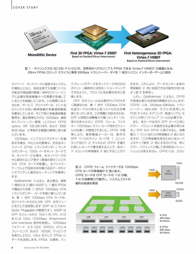
クプレーンがデータをネットワーク内の次のポイント ( 最終的には宛先 ) にルーティングできるように、プロトコルを必要な形式に変換します。 CFP 光モジュールは比較的サイズが大きく高価なため、第 1 世代 100Gbps OTN 伝送カードの小型化と低コスト化の主な障害になっています。この問題に対処するため、CFP と同等の消費電力で幅 ( ピッチ ) 1/2、深さは多少小さい CFP2 フォーム ファクター (100Gbps ライン カード用光モジュールの定義 ) が開発されました。CFP2 の登場により、通 信 機 器メーカーは、既存 の CFP ベースのライン カードを 1 ユニット エリア当たり 2 チャネルの CFP2 を備えた新しいカードで置き換えることで、各カード スロットの帯域幅を 2 倍にすることがで
きます。これにより、データセンター全体の帯域幅を 2 倍に拡張できる可能性があります ( 図 2 を参照 )。 しかし、Goldhammer によると、CFP2 の登場は新たな技術的課題をもたらします。
「CFP2 には、25Gbps/28Gbps トランシーバー、IBIS-AMI モ デル を 使 用した PCB チャネル モデリング、高速シリアル モデリング用ソフトウェア ツールが必要です。 また、各カードは元の CFP カードと同じパワー バジェットを維持する必要があります。」CFP から CFP2 に移行すると、消費電力 1 ワット当たりの帯域幅は 2 倍になりますが、「この帯域幅を得るために各カード上のチップ数を 2 倍にするだけでは、特にパワー バジェットに関して実用的なソリューションとは言えません。CFP2 には、さらに
C O V E R S T O R Y
CFP
CFP2 CFP2 CFP2 CFP2 CFP2 CFP2 CFP2 CFP2
CFP CFP CFP
100G CFPOPTICS
CFP2OPTICS
CAUI
CAUI4
10x10G
4x25G
100G
4 CFPs400 Gbps60 Watts
8 CFP2s800 Gbps60 Watts
図 1 – ザイリンクスの 3D SSI テクノロジが、世界初のヘテロジニアス FPGA である Virtex-7 H580T の基礎となる。28nm FPGA ロジック スライスと専用 28Gbps トランシーバー ダイを 1 枚のシリコン インターポーザー上に統合
図 2 – CFP2 フォーム ファクターでは 100Gbps OTN カードの帯域幅が 2 倍に拡大。CFP2 カードは CFP カードの 1/2 の幅、1/2 の消費電力で動作し、システムコストの劇的な削減を実現
8 Xcell Journal 79・80 合併号
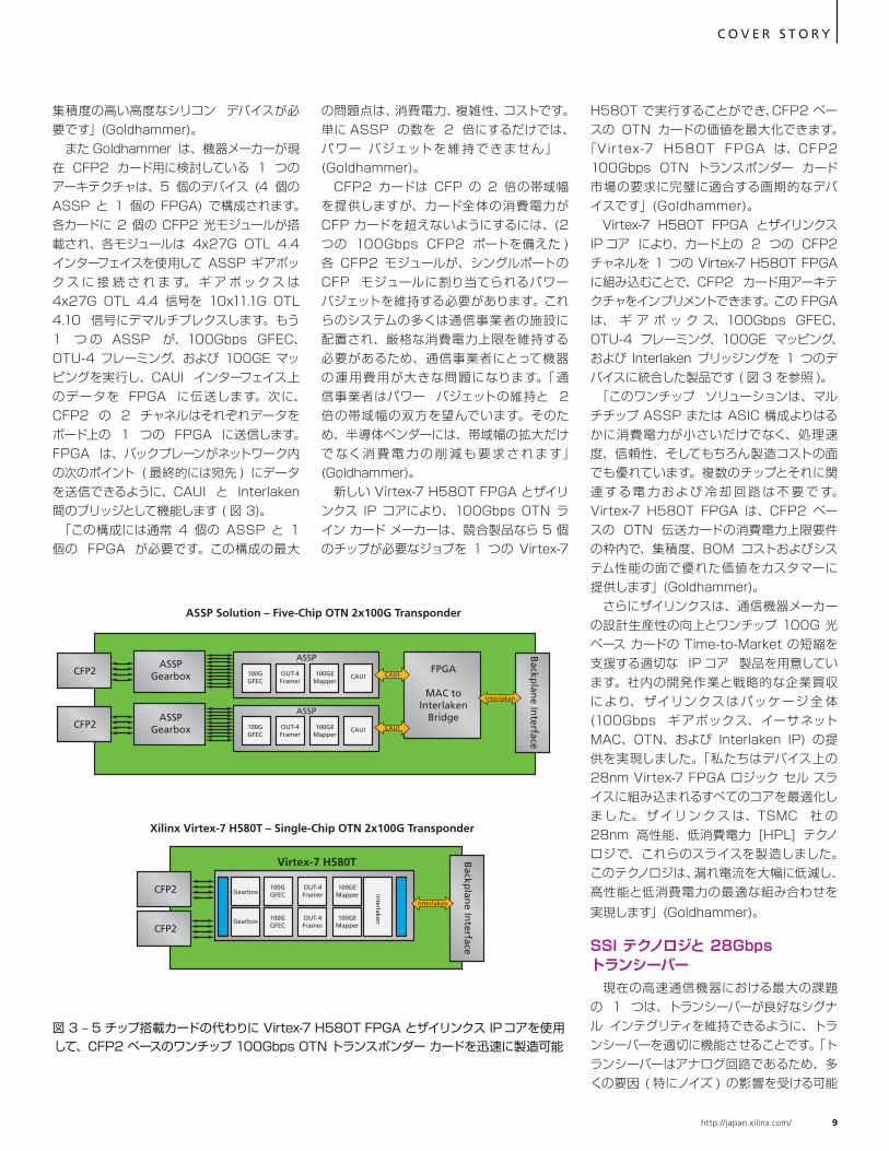
集積度の高い高度なシリコン デバイスが必要です」(Goldhammer)。 また Goldhammer は、機器メーカーが現在 CFP2 カード用に検討している 1 つのアーキテクチャは、5 個のデバイス (4 個の ASSP と 1 個の FPGA) で構成されます。各カードに 2 個の CFP2 光モジュールが搭載され、各モジュールは 4x27G OTL 4.4 インターフェイスを使用して ASSP ギアボック ス に 接 続 さ れ ま す。 ギ ア ボック ス は 4x27G OTL 4.4 信号を 10x11.1G OTL 4.10 信号にデマルチプレクスします。もう 1 つ の ASSP が、100Gbps GFEC、OTU-4 フレーミング、および 100GE マッピングを実行し、CAUI インターフェイス上のデータを FPGA に伝送します。次に、CFP2 の 2 チャネルはそれぞれデータをボード上の 1 つの FPGA に送信します。FPGA は、バックプレーンがネットワーク内の次のポイント ( 最終的には宛先 ) にデータを送信できるように、CAUI と Interlaken 間のブリッジとして機能します ( 図 3)。 「この構成には通常 4 個の ASSP と 1 個の FPGA が必要です。この構成の最大
の問題点は、消費電力、複雑性、コストです。単に ASSP の数を 2 倍にするだけでは、パワー バジェットを維持できません」(Goldhammer)。 CFP2 カードは CFP の 2 倍の帯域幅を提供しますが、カード全体の消費電力が CFP カードを超えないようにするには、(2 つの 100Gbps CFP2 ポートを備えた ) 各 CFP2 モジュールが、シングルポートの CFP モジュールに割り当てられるパワー バジェットを維持する必要があります。これらのシステムの多くは通信事業者の施設に配置され、厳格な消費電力上限を維持する必要があるため、通信事業者にとって機器の運用費用が大きな問題になります。「通信事業者はパワー バジェットの維持と 2 倍の帯域幅の双方を望んでいます。そのため、半導体ベンダーには、帯域幅の拡大だけでなく消 費 電 力の削 減も要求 されます」(Goldhammer)。 新しい Virtex-7 H580T FPGA とザイリンクス IP コアにより、100Gbps OTN ライン カード メーカーは、競合製品なら 5 個のチップが必要なジョブを 1 つの Virtex-7
H580T で実行することができ、CFP2 ベースの OTN カードの価値を最大化できます。
「Virtex-7 H580T FPGA は、CFP2 100Gbps OTN トランスポンダー カード市場の要求に完璧に適合する画期的なデバイスです」(Goldhammer)。 Virtex-7 H580T FPGA とザイリンクス IP コア により、カード上の 2 つの CFP2 チャネルを 1 つの Virtex-7 H580T FPGA に組み込むことで、CFP2 カード用アーキテクチャをインプリメントできます。この FPGA は、 ギ ア ボ ッ ク ス、100Gbps GFEC、OTU-4 フレーミング、100GE マッピング、および Interlaken ブリッジングを 1 つのデバイスに統合した製品です ( 図 3 を参照 )。 「このワンチップ ソリューションは、マルチチップ ASSP または ASIC 構成よりはるかに消費電力が小さいだけでなく、処理速度、信頼性、そしてもちろん製造コストの面でも優れています。複数のチップとそれに関連 する電 力および 冷 却回 路 は不 要 で す。Virtex-7 H580T FPGA は、CFP2 ベースの OTN 伝送カードの消費電力上限要件の枠内で、集積度、BOM コストおよびシステム性能の面で優れた価値をカスタマーに提供します」(Goldhammer)。 さらにザイリンクスは、通信機器メーカーの設計生産性の向上とワンチップ 100G 光ベース カードの Time-to-Market の短縮を支援する適切な IP コア 製品を用意しています。社内の開発作業と戦略的な企業買収により、ザイリンクスはパッケージ 全 体 (100Gbps ギアボックス、イーサネット MAC、OTN、および Interlaken IP) の提供を実現しました。「私たちはデバイス上の 28nm Virtex-7 FPGA ロジック セル スライスに組み込まれるすべてのコアを最適化しました。 ザイリン ク ス は、TSMC 社 の 28nm 高性能、低消費電力 [HPL] テクノロジで、これらのスライスを製造しました。このテクノロジは、漏れ電流を大幅に低減し、高性能と低消費電力の最適な組み合わせを実現します」(Goldhammer)。
SSI テクノロジと 28Gbps トランシーバー 現在の高速通信機器における最大の課題の 1 つは、トランシーバーが良好なシグナル インテグリティを維持できるように、トランシーバーを適切に機能させることです。「トランシーバーはアナログ回路であるため、多くの要因 ( 特にノイズ ) の影響を受ける可能
C O V E R S T O R Y
CFP2ASSP
Gearbox
Backp
lane In
terface
FPGA
MAC toInterlaken
Bridge
100GGFEC
CAUI CAUI
Interlaken
OUT-4Framer
ASSP
100GEMapper
CFP2
CFP2
Backp
lane In
terface
CFP2
ASSPGearbox 100G
GFECCAUI CAUIOUT-4
Framer
ASSP
100GEMapper
100GGFEC
OUT-4Framer
100GEMapper
100GGFEC
Gearbox
Virtex-7 H580T
Xilinx Virtex-7 H580T – Single-Chip OTN 2x100G Transponder
ASSP Solution – Five-Chip OTN 2x100G Transponder
OUT-4Framer
100GEMapper
Gearbox
Interlaken
Interlaken
図 3 – 5 チップ搭載カードの代わりに Virtex-7 H580T FPGA とザイリンクス IPコアを使用して、CFP2 ベースのワンチップ 100Gbps OTN トランスポンダー カードを迅速に製造可能
http://japan.xilinx.com/ 9
性がある」と、Goldhammer は述べています。「大半のミックスド シグナル デバイスでは、トランシーバーは通常はデバイスのエッジに分離されて配置され、デバイス中央部のデジタル回路から遮蔽されます。それが、デジタル回路はノイズが発生しやすいため、通常はアナログ回路から分離される理由です」(Goldhammer)。 過去 10 年間、通信機器業界は、Gbps/秒レベルの帯域幅を実現するために、高速信号の送受信に高速アナログ トランシーバーを利用してきました。従来の経験則では、トランシーバーの帯域幅を拡大するほど、安定したシグナル インテグリティの確保は困難になります。 また、Virtex-7 H580T FPGA は高度に集積されたワンチップ SSI テクノロジ ソリューションであるため、Virtex-7 H580T FPGA を採用した CFP2 ベースのライン カードは性能が大幅に向上します。「4x25G インターフェイスへの移行により、10x10G インターフェイスの配線の複雑性が大幅に軽減されます。25G/28G トランシーバーに関する懸念も一部に存在しますが、ザイリン
クスの SSI テクノロジにより、この複雑性を大幅に軽減できます。ノイズに敏感なアナログ回路を備えた 28G トランシーバーは、デジタル ロジック回路から物理的に分離されます。このアーキテクチャでは、トランシーバー対応デジタル ダイからの十分な分離が確保されます」(Goldhammer)。 Goldhammer によると、28G トランシーバーは高速プロセス テクノロジで製造され、クラス最高の品質が確保されます。「一方、FPGA スライスは 28nm HPL で製造され、総消費電力が最小限に抑えられます。」その結果、Virtex-7 H580T FPGA 上では 28Gbps トランシーバーの素晴らしい高性能とシグナル インテグリティが実現されます。これらのトランシーバーの実際の使用例については、YouTube で次のビデ オ をご 覧くだ さ い。http://www.you-tube.com/watch?v=FFZVwSjRC4c&-feature=player_profilepage Goldhammer によると、SSI アーキテクチャで実現される物理的分離により、ザイリンクスは Virtex-7 H580T FPGA に 8 個の 28Gbps トランシーバーを搭載し
ました。これは最も大規模な競合デバイスに搭載されているトランシーバー数の 2 倍に相当します。 さらに印象的なことに、ザイリンクスの 28nm フ ァ ミ リ に は、 今 後 Virtex-7 H580T FPGA よりもさらに上位のトランシーバー デバイスが登場します。まもなくザイリンクスは Virtex-7 H870T の出荷を開始します。このデバイスは、16 個の 28Gbps ト ラ ン シ ー バ ー、72 個 の 13.1Gbps トランシーバー、876,160 個の ロ ジ ッ ク セ ル を 搭 載 し て い ま す。Goldhammer によると、H580T デバイスのすべてのトランシーバー機能を使用した場合、合計 2.78 テラバイト / 秒のシリアル接続を実現する機器の設計が可能となります。 「1 個のモノリシック FPGA 上に多数の 28Gbps トランシーバーを配置したデバイスは、実用性に乏しく高コストです。幸いなことに、SSI テクノロジにより、ザイリンクスは現在 8 個~16 個の 28Gbps トランシーバーを備えた拡張性の高い FPGA ファミリ を 製 造 で き ま す」(Goldhammer)。ASSP メーカーやほかの FPGA ベンダーの製品は、最大 4 個の 28G トランシーバーしか搭載していません。これは 40nm および 28nm プロセスでモノリシック デバイスに 28Gbps トランシーバーを配置する作業の困難さの現われです。 Virtex-7 H870T デバイスは、有線通信の次世代となる 400G 市場を対象としています。「400G 市場は遠い先にあり、存在するとしても、各企業は研究に着手した段階であり、標準化団体による規格もまだ策定されていません。素晴らしいことに、ザイリンクスはすでに 400G 市場を見据えたデバイスを用意しています。私たちは 400G 対応機器の開発とイノベーションのスピードアップを支援できます」(Goldhammer)。 ザイリンクスはまた、重要カスタマーへの Virtex-7 H580T FPGA の最初のシリコン の 出 荷 を し て い ま す。 ま た 最 新 の Vivado ™ Design Suite 内の開発ツールの サ ポ ー ト も 利 用 で き ま す。Virtex-7 H580T デバイスに興味をお持ちの方は、価格と供給状況の詳細を最寄りのザイリンクス販売代理店までお問い合わせください。 ザイリンクスの 28Gbps シリアル トランシーバー テクノロジに関する新しいホワイト ペーパーとビデオは、http://japan.xilinx.com/products/technology/transceiv-ers/index.htm でご覧いただけます。
C O V E R S T O R Y
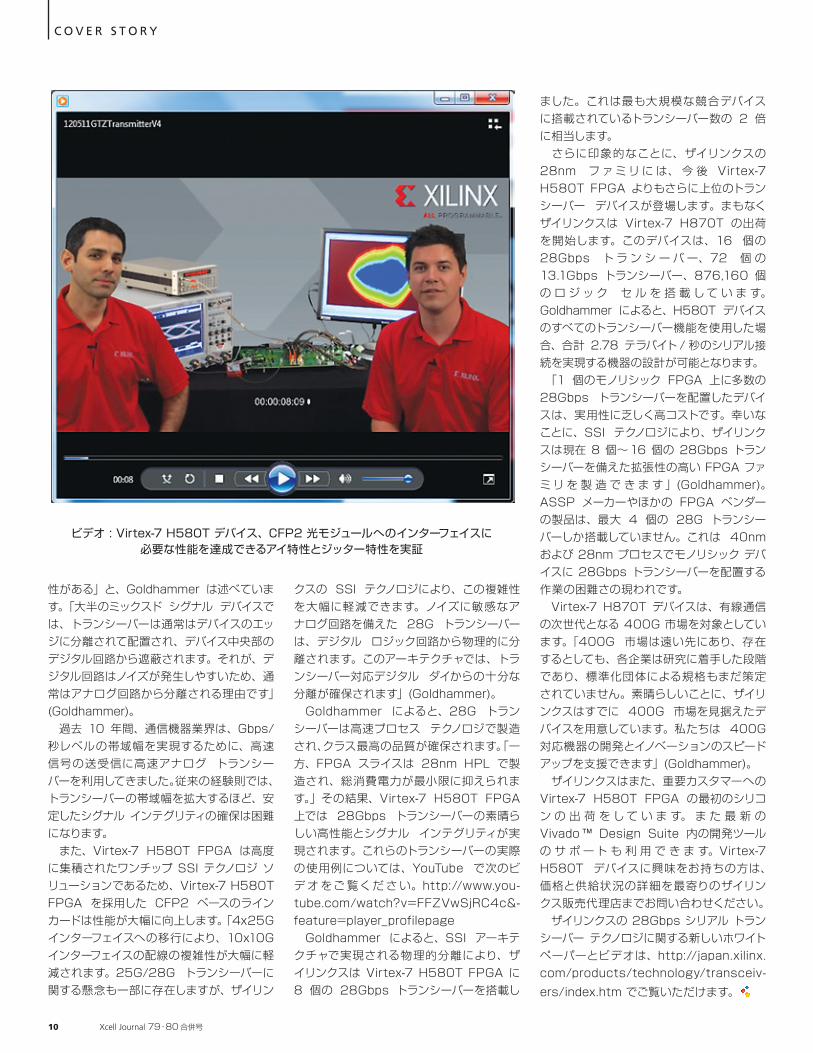
ビデオ : Virtex-7 H580T デバイス、CFP2 光モジュールへのインターフェイスに必要な性能を達成できるアイ特性とジッター特性を実証
10 Xcell Journal 79・80 合併号
VivadoTM Design Suite WebPACKTM Edition で比類なきインテグレーションおよびインプリメンテーション タイムを実現
詳細はこちら
■東京エレクトロン デバイス(株) TEL(045)443-4016 [email protected] ■アヴネット ジャパン(株) TEL(03)5792-8210 [email protected] ■(株)PALTEK TEL(045)477-2005 [email protected]■富士通エレクトロニクス(株) TEL(045)415-5825 [email protected] ■新光商事(株) TEL(03)6361-8086 X-Pro@shinko-sj.co.jp©Copyright 2013 Xilinx, Inc. All rights reserved. ザイリンクスの名称およびロゴ、Vivado、WebPACKは米国およびその他各国のザイリンクス社の登録商標および商標です。
COVER STORY
Xilinx Unveils Vivado Design Suite for the Next Decade of ‘All Programmable’ Devices
最先端の EDA テクノロジと手法をベースに開発された新しいツール スイートが登場デザインの生産性と性能の向上をもたらし、チップ数を抑えた高度なシステム開発を短期間で実現
ザイリンクスは、4 年にわたる開発と 1 年間のベータ版での検証を経て、Vivado ™ Design Suite の提供を、昨年夏のパブリック アクセスを目前にまずはアーリー アクセス プログラムの参加ユーザー向けに開始し、好評を得ています。Vivado は、IC レベルでの設計ツールの枠を超えた、システム レベルの高い統合デザイン環境を提供し、ツール間でメモリ共有が可能な拡張モデルと共通のデバッグ環境をベースに構築されています。また、業界標準である AMBA® AXI4 インターコネクトや IP-XACT IP パッケージ メタデータ、Tool Command Language (TcL)、Synopsys Design Constraints (SDC) などを基盤に構築されているため、ユーザーのデザイン ニーズを汲み取ったオープンな環境を提供します。Vivado Design Suite は、あらゆるタイプのプログラマブル テクノロジのデザインに最適化されているだけでなく、1 億ゲート ASIC 相当のデザインへのスケール アップも実現できるように構築されています。
Mike SantariniPublisher, Xcell JournalXilinx, [email protected]
ザイリンクス、次の 10 年の「All Programmable」デバイスに対応する Vivado Design Suite を提供
12 Xcell Journal 79・80 合併号
ザイリンクスのコーポレート ストラテジおよびマーケティング担当シニア バイス プレジデント、Steve Glaser は「この 4 年間でザイリンクスは、プログラマブル ロジック兼 I/O の枠を超え、ソフトウェアでのプログラマビリティを持つ ARM サブシステムから 3D IC、アナログ ミックスド シグナルまで、プログラマビリティ性を大きく拡張した All Programmable デバイスの開発、提供を行う企業へと革新しました。業界で数々の賞を受賞した Zynq ™ -7000 All Programmable SoC や 3D スタックド シリコン インターコネクト (SSI) テクノロジを採用した Virtex®-7 デバイスなど世界的に最先端の FPGA 製品とともに新しいレベルのプログラマブル システム インテグレーションを可能にしました。そして今、Vivado によって、ユーザーが来る 10 年におけるこれらの All Programmable デバイスを使ったデザインを行う際の生産性を飛躍的に向上させる最先端ツール スイートを提供します」と述べています。 ザイリンクスは All Programmable デバイスを開発しましたが、ユーザーはこれらデバイスを使用することで、新しいレベルのプログラマブル システムのインテグレーションが可能になり、BOM コストの削減や総システム消費電力の低減だけでなく、引いてはデザインの生産性向上が実現し、より早く製品の市場投入ができるようになります。ザイリンクスにとってこの実現に必要だったのは、インテグレーションおよびインプリメンテーションにおける尽きることのないボトルネックに対応できる、All Programmable デバイスと同様に革新的な設計ツール スイートを開発することだったと Glaser は指摘しています。 Glaser はインテグレーションに伴う問題として、(1) C 言語および RTL (Register-Transfer Level) レベルのアルゴリズム IP のインテグレーション、(2) DSP やエンベデッド、コネクティビティ、ロジックの混在、(3) ブロック単位およびシステム全体の検証、(4) デザインおよび IP コア の再利用、を挙げています。インプリメンテーションに関しては、(1) 階層的なチップ プランニングとパーティショニング、(2) マルチドメインおよびマルチダイの物理的な最適化、(3) 複数変数「デザイン」対「タイミング」クロージャ、(4) 設計後半の ECO (Engineering
Change Order) および変更による波及的な影響、などをボトルネックとしてあげています。新しい Vivado Design Suite は、これらボトルネックを解消し、ユーザーが All Programmable デバイスを使用したシステムのインテグレーションにおいてその性能を最大限に活かせるよう強力なツール スイートを提供します。 ザイリンクスは、Vivado Design Suite を開発するにあたり、業界標準規格を積極的に活用すると共に、最先端の EDA テクノロジと設計手法を採用しました。この結果、高度に自動化したプッシュボタン フローを求めるユーザーから、自身で細部にわたって調整を行いたいと考えるユーザーまで、あらゆる設計者が利用できるツール スイートが完成しました。しかも、これまでの使い慣れた直感的なルック アンド フィールはそのままで最先端の EDA 環境を利用でき、ザイリンクスの最も大規模なデバイスでさえも、従来よりもはるかに短時間で効率的に設計することができます。 Vivado Design Suite は、長い間主要なデザイン ツールとして提供されてきた ISE® Design Suite の機能をはるかにしのぐ、システム レベルの完全なプログラマブル機能を備えた最新のツール セットです。7 シリーズ FPGA やそれ以前のザイリンクス FPGA デバイスを使用したユーザー デザインのスムーズな移行を支援するために、ザイリンクスは今後も ISE の開発とサポートを無期限かつ継続的に提供する予定です。近い将来、7 シリーズ FPGA 以降のザイリンクス デバイスをすべてサポートする Vivado Design Suite が主要なデザイン環境となるでしょう。 ザイリンクスのデザイン メソドロジ マーケティング担当シニア ディレクター、Tom Feist は、Vivado Design Suite の ISE からの優位性は実際に使用してみればすぐに体感できると話しています。 「Vivado Design Suite は競合ツールに比べランタイムが 4 倍に向上しているほか、S y s t e mVe r i l o g、S D C 、C / C + +/SystemC、ARM 社の AMBA® AXI バージョン 4 インターコネクト、インタラクティブな TcL スクリプトなどの業界標準規格を採用しており、ユーザーの生産性が大きく向上します。その他の特長として、Vivado では数多くのレポートやデザイン ビューを提
供しており包括的なクロスプローブが実行できたり、最先端のグラフィックスを利用して容易に IP コア の統合ができたりします。特に見逃せないのは、C++ から HDL への高位合成を FPGA ベンダーの市販ツールとして初めて完全サポートした点です」(Feist)。
次世代プログラマブル デザインに向けたツール ザイリンクスが ISE Design Suite を発表したのは 1997 年のことでした。このツール スイートには、1995 年 4 月にザイリンクスが買収した NeoCAD 社の当時としては極めて画期的なタイミング ドリブンの配置・配線エンジンが使用されていました。 その後の 15 年間、FPGA で実行可能な機能が次第に複雑化していくのに合わせ、ザイリンクスは ISE Design Suite に多言語対応の合成 / シミュレーション、IP コア の統合、そして編集 機能やテスト機能など、さまざまな新技術を追加し、デザイン ツールとしての機能を全面的に改良してきました。ザイリンクスは、新しい Vivado Design Suite の開発にあたり、ISE で培った経験を最大限に活かし、ISE の主要な技術を引き継ぎつつも最新の EDA アルゴリズム、ツール、手法を積極的に取り入れたと Feist は述べています。 「Vivado Design Suite は今日のデザイン の 生 産 性 を 大 幅 に 高 め る と 同 時 に、20nm 以降のシリコンで課題となる容量とデザインの複雑性にも容易に対応できる拡張性を備えています。EDA テクノロジはこの 15 年間で飛躍的な進歩を遂げてきました。Vivado Design Suite はまったくゼロから開発されているため、最新の EDA テクノロジや標準規格への対応も万全で、当面のデザインに対応可能な優れた拡張性を備えたツールに仕上がっています」(Feist)。
確定的なデザイン クロージャ 一般に、FPGA ベンダーが提供する統合設計ツールは、物理インプリメンテーション フロー ( 合成、フロアプランニング、配置・配 線、 電 力 / タイミ ン グ 解 析、 最 適 化、ECO) が中心となって構成されています。Vivado Design Suite では最先端のインプリメンテーション フローが構築されているため、短期間でデザイン クロージャを達成できます。
C O V E R S T O R Y
ザイリンクス、次の 10 年の「All Programmable」デバイスに対応する Vivado Design Suite を提供
http://japan.xilinx.com/ 13
スケーラブルなデータ構造アーキテクチャ ザイリンクスは、設計の反復を削減して全体的な設計期間を短縮し、総合的な生産性を高めるために、実メモリ上でスケーラブルなデータ構造を共有するインプリメンテーション フローを構築しました。このフレームワークは、現在最先端の ASIC デザイン環境でも一般的に採用されているものです。「実メモリ上でスケーラブルなデータ構造を共有することで、合成、シミュレーション、フロアプランニング、配置配線などデザイン フローの各段階においてインメモリのデータ構造で動作させることができます。このため、各設計プロセスでデバッグと解 析が行え、ユーザーはタイミング、消費電力、リソース使用率、配線密集などのデザインの評価に不可欠な値をかなり早い段階で測定できます。これらの予測値は、インプリメンテーションの工程が進むにつれて精度が増していきます」(Feist)。 単一のデータ構造を共有することによる特に大きな利点として、新しい多次元解析型配置配線エンジンを、Vivado Design Suite の RTL 合成エンジンや新しい多言語シミュレーション エンジン、IP Integrator、Pin Editor、Floor Planner、Device Editor などの各ツールと密接に連携できる
ようになったことが挙げられます。 Vivado Design Suite の包括的なクロスプローブ機能を利用することで、回路図やタイミング レポート、ロジック セルの問題に対してさまざまなビューに切り替えて HDL コードにまでさかのぼって追跡とクロスプローブが行えます。 「各設計プロセスで解析ができるようになっただけでなく、それらすべてのプロセスが相互につながっています。合成後のフローでも、各プロセスでタイミング、消費電力、ノイズ、リソース使用率を解析することができます。タイミングや消費電力の目標を達成できていないことが早い段階で明らかになれば、配置配線後に設計の反復を何度も繰り返すことなくより短い時間で設計の見直しが可能で、問題解決に向けて早めに手を打つことができます」(Feist)。 スケーラブルなデータ構造によって緊密な連携が実現したことにより、なるべく多くの 作 業 を 自 動 で 実 行した い と 考 えるユーザーに対しては、より効 果 的なプッシュボタン フローを提 供で きるようになったと Feist は述べています。同時に、あらゆる設 計プロセスでデザインをきめ細かく制御するユーザーへは、高度な解析機能やコマンドも用意されていると付け加えています。
階層型のチップ プランニングと高速合成 Vivado Design Suite にはデザインを複数に分割する機能を提供しており、大規模なプロジェクトを複数のチームで分割して合成およびインプリメンテーション、検証を分割統治法で行うことができると Feist は説明しています。新しいデザイン保持機能によりタイミング結果の再現性が維持され、デザインのパーシャル リコンフィギュレーションも可能です。 Vivado Design Suite には、数百万ロジック セルに対応したまったく新しい合成エンジンも搭載されています。この合成エンジンで特に注目されるのが、SystemVerilog サポートの強化です。「Vivado の合成エンジンは SystemVerilog 言語の合成可能サブセットへの対応がほかのどの市販ツールよりも充実しています」(Feist)。このエンジンは ISE Design Suite に含まれる XST (Xilinx Synthesis Technology) の 3 倍高速で、デザインの面積とサイズの大まかな見積もりを短時間で得られる「クイック」オプションもサポートしています。このため、RTL またはゲートレベル回路図でのデバッグに必要な時間が 1/15 に短縮されます。 また、多くの ASIC 設計者がプログラマブル プラットフォームへ移行するなか、
C O V E R S T O R Y
25
20
15
10
5
00.0E+00 5.0E+05 1.0E+06 1.5E+06 2.0E+06
12h/MLC
4.6h/MLC
Vivado
ISE
Competitor tools
Ru
nti
me
(ho
urs
)
Design size (LC)
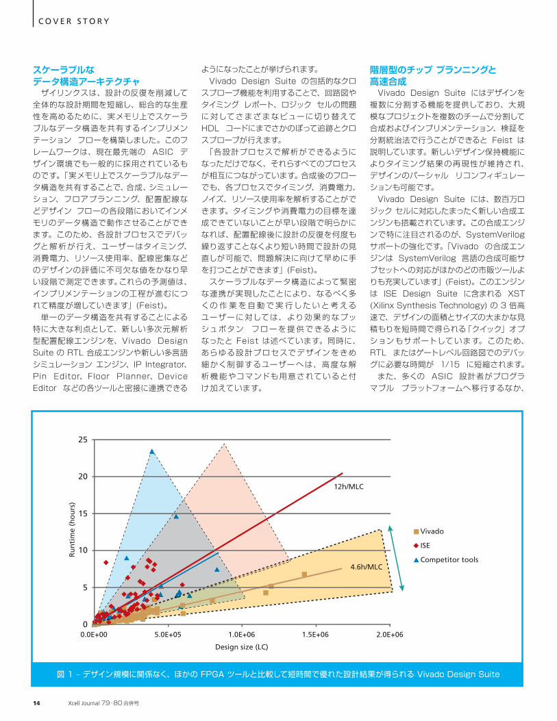
図 1 – デザイン規模に関係なく、ほかの FPGA ツールと比較して短時間で優れた設計結果が得られる Vivado Design Suite
14 Xcell Journal 79・80 合併号
ザイリンクスは Vivado フロー全体で Synopsys Design Constraints を採用しています。この業界標準規格を採用することで新たなレベルでの自動化が可能になり、制約の生成、クロック ドメイン間のチェック、フォーマル検証、あるいは Synopsys 社が提供する PrimeTime などのツールを利用したスタティック タイミング解析 (STA) など、業界最先端の EDA ツールを使用してさまざまなタスクを実行できます。
多次元解析に対応した配置エンジン これまで FPGA ベンダーが提供してきた旧世代のデザイン ツール スイートには、シミュレーテッド アニーリング (SA) アルゴリズムを使用した 1 次元のタイミングドリブン配置配線エンジンが使用されてきたと Feist は説明しています。これらのエンジンは、ツールがロジック セルを配置する場所をランダムに決定します。このような配線エンジンでは、ユーザーがタイミングを入力すると、可能な限りタイミング要件が満たされるよう SA アルゴリズムが擬似的に機能を配置します。「以前はデザインの規模がかなり小さく、ロジック セルが遅延の最大要因であったため、こうした方法でも十分通用していました。現在ではデザインの複雑化とシリコン プロセスの微細化により、インターコネクトと配線密度がはるかに大きな遅延の要因となっています」(Feist)。
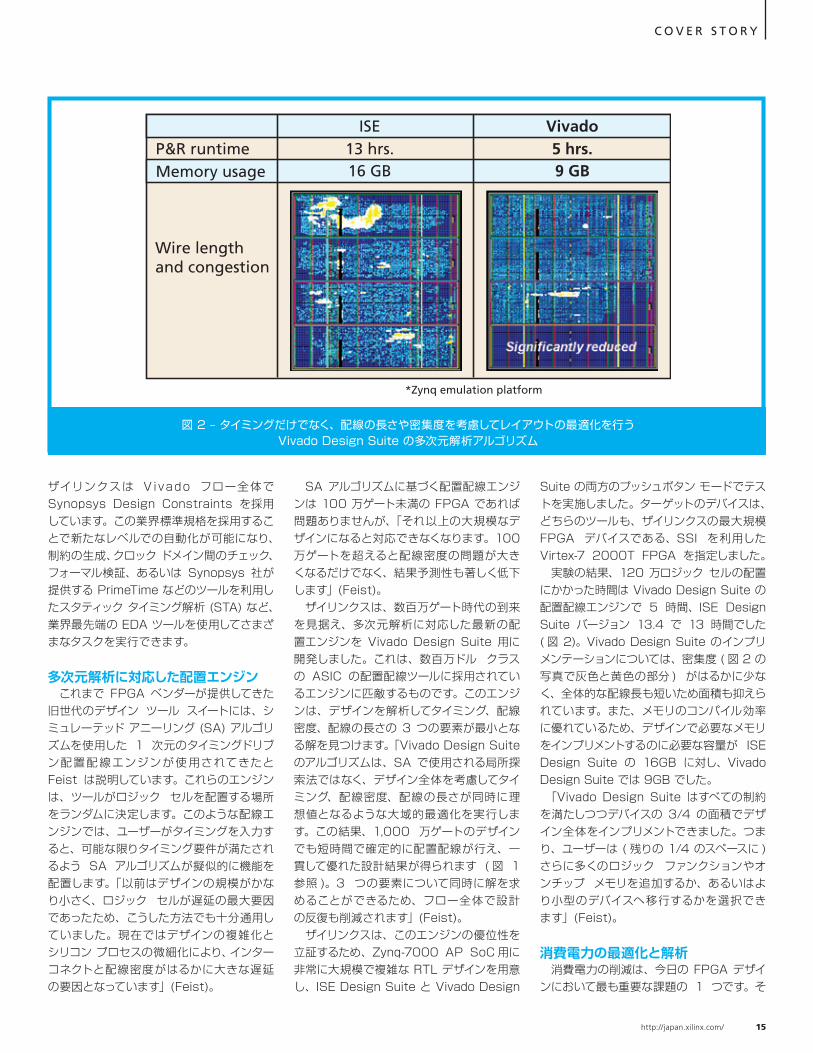
SA アルゴリズムに基づく配置配線エンジンは 100 万ゲート未満の FPGA であれば問題ありませんが、「それ以上の大規模なデザインになると対応できなくなります。100 万ゲートを超えると配線密度の問題が大きくなるだけでなく、結果予測性も著しく低下します」(Feist)。 ザイリンクスは、数百万ゲート時代の到来を見据え、多次元解析に対応した最新の配置エンジンを Vivado Design Suite 用に開発しました。これは、数百万ドル クラスの ASIC の配置配線ツールに採用されているエンジンに匹敵するものです。このエンジンは、デザインを解析してタイミング、配線密度、配線の長さの 3 つの要素が最小となる解を見つけます。「Vivado Design Suite のアルゴリズムは、SA で使用される局所探索法ではなく、デザイン全体を考慮してタイミング、配線密度、配線の長さが同時に理想値となるような大域的最適化を実行します。この結果、1,000 万ゲートのデザインでも短時間で確定的に配置配線が行え、一貫して優れた設計結果が得られます ( 図 1 参照 )。3 つの要素について同時に解を求めることができるため、フロー全体で設計の反復も削減されます」(Feist)。 ザイリンクスは、このエンジンの優位性を立証するため、Zynq-7000 AP SoC 用に非常に大規模で複雑な RTL デザインを用意し、ISE Design Suite と Vivado Design
Suite の両方のプッシュボタン モードでテストを実施しました。ターゲットのデバイスは、どちらのツールも、ザイリンクスの最大規模 FPGA デバイスである、SSI を利用した Virtex-7 2000T FPGA を指定しました。 実験の結果、120 万ロジック セルの配置にかかった時間は Vivado Design Suite の配置配線エンジンで 5 時間、ISE Design Suite バージョン 13.4 で 13 時間でした ( 図 2)。Vivado Design Suite のインプリメンテーションについては、密集度 ( 図 2 の写真で灰色と黄色の部分 ) がはるかに少なく、全体的な配線長も短いため面積も抑えられています。また、メモリのコンパイル効率に優れているため、デザインで必要なメモリをインプリメントするのに必要な容量が ISE Design Suite の 16GB に対し、Vivado Design Suite では 9GB でした。 「Vivado Design Suite はすべての制約を満たしつつデバイスの 3/4 の面積でデザイン全体をインプリメントできました。つまり、ユーザーは ( 残りの 1/4 のスペースに ) さらに多くのロジック ファンクションやオンチップ メモリを追加するか、あるいはより小型のデバイスへ移行するかを選択できます」(Feist)。
消費電力の最適化と解析 消費電力の削減は、今日の FPGA デザインにおいて最も重要な課題の 1 つです。そ
C O V E R S T O R Y
ISE13 hrs.P&R runtime
Memory usage
*Zynq emulation platform
Wire lengthand congestion
16 GB
Vivado5 hrs.9 GB
図 2 – タイミングだけでなく、配線の長さや密集度を考慮してレイアウトの最適化を行う Vivado Design Suite の多次元解析アルゴリズム
http://japan.xilinx.com/ 15
こで、Vivado Design Suite では高度な消費電力最適化手法を利用してユーザー デザインの消費電力をさらに削減できるようにしています。「Vivado Design Suite は現在最先端の ASIC ツール スイートで採用されているものと同等の高度なクロック ゲーティング手法を使用しており、デザインのロジックを解析してクロック ゲーティングを適用することで、不必要なスイッチング動作を取り除くことができます。この新しいテクノロジで特に着目しているのが、スイッチング動作の α 係数です。ダイナミック消費電力については最大 30% の削減が可能です。これは ISE Design Suite で昨年採用したものと同じテクノロジですが、今後は Vivado で継続的に改良されていくことになるでしょう」(Feist)。 さらに、実メモリ上でスケーラブルなデータ 構 造 を 共 有 可 能 な Vivado Design Suite は、デザイン フローの各段階において消費電力を予測できるため、アップフロント解析を実行してデザインの初期段階で問題のある部位を修正できると Feist は説明しています。
ECO の簡略化 インクリメンタル フローでは、小規模な変更であればデザインを部分的に再度インプリメントするだけで簡単に処理できるため、変更後の設計の反復が短時間で完了するという利点があります。しかも段階的な変更ごとのパフォーマンスをインクリメンタル方式で維持することができるため、設計の反復を何度も繰り返す必要がありません。Vivado Design Suite では、定番の ISE FPGA Editor を拡張した Vivado Device Editor を提供していますが、これを使用することでこれを実現します。配置配線済みデザインで Vivado Device Editor を使用すると、インスタンスの移動、ネット配線の変更、スコープでデバッグするための主要出力へのレジスタ追加、DCM (Digital Clock Manager) や LUT (Lookup Table) のパラメーター変更といった ECO (Engineering Change Order) が設計段階の終盤に発生しても、合成やインプリメンテーションをやり直す必要がありません。これほどの柔軟性を備えた FPGA デザイン環境はほかにないと Feist は述べています。
フローの押し付けではなく、自動化を目指す ザイリンクスのツール 開 発 チ ーム は、
Vivado Design Suite の開発にあたり、ツールがフローを押し付けるのではなく、フローの自動化を図ることを目指しました。「C、C+ +、SystemC、VHDL、Ver i log、SystemVerilog、MATLAB®、Simulink®
など、ユーザーがどのような形から設計を開始しても、またザイリンクスの IP コアを使用しているかサードパーティ提供の IP コア を使用しているかにかかわらず、自動化されたフローによってユーザーの生産性が向上します。さらに、スキル レベルや好みがユーザーによって異なることも考慮に入れました。プッシュボタン フローを好むユーザーもいれば、設計段階ごとに独自で解析を行いたいとするユーザーもいます。また、GUI は初心者向けと考えてあらゆる処理をコマンド ラインまたは TcL を使用したバッチ モードで実行しようとするユーザーもいます。このツール スイートは、あらゆるユーザー ニーズに応えられる柔軟性の高い機能を各種提供しています」(Feist)。
IP Packager、IP Integrator、Extensible IP Catalog ザイリンクスのツール開発チームは、IPコア の作成や統合、アーカイブをサポートする専用の IP コア機能を追加することを最重要目標として Vivado Design Suite の開発にあたりました。こうして用意されたのが、IP Packager、IP Integrator、Extensible IP Catalog と呼ばれる 3 つの IP 機能です。 「現在では、IP コアをまったく含まない IC はほとんど存在しません。業界標準規格を採用し、IP コアの作成、統合、アーカイブ/ 保守管理をサポートする専用のツールを提供することで、エコシステムの IP コア ベンダーやユーザーが短期間で IP コアを作成し、デザインの生産性を向上できるようサポートしています。既に 20 社以上のベンダーからこの新しいツール スイートに対応した IP コアが提供されています」(Feist)。 IP Packager を利用することで、ザイリンクス製品のユーザーや IP コアの開発者、エコシステム パートナーは、あらゆる設計段階 (RTL、ネットリスト、配置済みネットリスト、配置配線済みネットリスト ) でデザインの一部または全体を再利用可能な IP コアに変換できます。このツールで作成した IP コアは IP-XACT 形式で記述されており、将来のデザインに容易に組み込むことができます。IP Packager は、各 IP コアのデータを XML ファイルで定義します。そして、このツールで
作成した IP コアは、IP Integrator を使用してデザイン全体に組み込むことができると Feist は解説しています。 「IP Integrator では、IP コアをピン レベルでなくインターコネクト レベルでデザインに統合できます。IP コアをデザインにドラッグ アンド ドロップすると、IP Integrator はまずそれぞれのインターフェイスに互換性があるかどうかをチェックします。互換性チェックが完了したら、コア間を 1 本の線で結ぶだけですべてのピンを接続した詳細な RTL が自動的に作成されます」(Feist)。 IP Integrator を使用し、たとえば 4、5 個のブロックをデザインにマージした場合、
「(そのプロセスの) 出力を再び IP Packager に戻すことができます。すると、その結果はほかのユーザーが再利用できる IP コアになります。しかもこの IP コアに変換できるのは RTL だけではなく、配置済みネットリスト、または配置配線済み IP ネットリスト ブロックも可能で、統合や検証にかかる時間がさらに短縮されます」(Feist)。 3 番目のツール、Extensible IP Catalog は、ユーザーが自身で作成した IP コアや、ザイリンクスまたはサードパーティ ベンダーによってライセンス付与された IP コア から独自の標準レポジトリを構築するためのツールです。このカタログは IP-XACT 規格の要件を満たすように開発されており、設計チームだけにとどまらず企業内全体で IP コアの管理が容易にできるようになり、組織全体で IP コアを共有することができます。Feist によると、Vivado Extensible IP Catalog にはザイリンクスの System Generator と IP Integrator が含まれているため、ユーザーはカタログに登録した IP にアクセスしてそれをデザイン プロジェクトに容易に組み込むことができるといいます。 Vivado プロダクト マーケティング担当ディレクター のラミネ ローン (Ramine Roane) は、「これまでは、サードパーティの IP ベンダーが IP コアを zip ファイルに圧縮し付属品として提供していましたが、これらの 新 し い ツ ー ル を 使 用 す れ ば Vivado Design Suite と互換性のある統一フォーマットで提供され、すぐに IP コアを利用できます」と述べています。
ESL の普及に弾みをつける Vivado HLS すでにリリースされている Vivado Design Suite に搭載された数多くの新技術で最も 将 来 を 見 据 え たも の は、2010 年 の
C O V E R S T O R Y
16 Xcell Journal 79・80 合併号
AutoESL 社買収によってザイリンクスが実現した Vivado HLS ( 高位合成 ) です。 ザイリンクスは市販の ESL (Electronic System-Level) デザイン ツールを広範に評価し、結果業界最高のツールを手に入れるにいたりました。この買収を決定する上でザイリンクスが参考にしたのが、調査会社 BDTI 社によるレポートでした ( 詳細は、Xcell Journal 71・72 合併号ページ 18 「DSP 中心の FPGA デザインへの高位合成フローの使用を BDTI が評価」 http://japan.xilinx.com/publications/archives/xcell/issue71-72/xcell71_72.pdf を参照 )。 「Vivado HLS は C、C++、SystemC を包括的にカバーしており、浮動小数点に加えて任意精度の浮動小数点 ( 演算 ) も行います。つまり、一般的なハードウェア環境ではなくアルゴリズム開発環境でもこのツールが使用できることを意味します。このレベルで開発したアルゴリズムは、RTL レベルよりも相当短い時間で検証が行えるという利点があります。これは単にシミュレーション時間が短縮できるというだけでなく、アルゴリズムの実現可能性を十分に検討した上で、スループットやレイテンシ、消費電力のトレードオフをアーキテクチャ レベルで行えるということにもつながります」(Feist)。 Vivado HLS はさまざまな機能を幅広い用途で提供していますが、ここでは、ユーザーが IP コアを開発してそれをデザインに組み込む際に利用できる一般的なフローを紹介します。 まず、ユーザーが C、C++、SystemC を使用してデザインを記述し、希望する動作を記述した C テストベンチを作成します。 次に、GNU Compiler Collection/G++ または Visual C++ シミュレータを用いてデザインのシステム動作を検証します。ビヘイビアー デザインの機能検証が完了し、付随するテストベンチを修正したら、Vivado HLS で合成を実行して Verilog または VHDL の RTL デザインを生成します。RTL の生成後、デザインの Verilog または VHDL シミュレーションを実行するか、Vivado HLS 上で C ラッパー テクノロジを使用して SystemC バージョンを作成するかを選択します。次に、SystemC アーキテクチャ レベルのシミュレーションを実行し、先に作成した C テストベンチを基準にしてデザインのアーキテクチャ上の動作と機能をさらに検証します。 デザインが確定したら、Vivado Design Suite の物理インプリメンテーション フ
ローを使用してデザインをデバイスにプログラムし、ハードウェアで動作させます。あるいは IP Packager を使用してデザインを再利用可能な IP コアに変換し、IP Integrator を用いてこの IP コアをデザインに組み込むか、または System Generator で動作させます。 このフローは Vivado HLS の 1 つの使用例に過ぎません。Xcell Journal 本号次章(ページ 18-22)に、アジレント・テクノロジー社の Nathan Jachimiec 氏とザイリンクスの Fernando Martinez Vallina が 共同で執筆した 「高レベル合成ツールによるパケット エンジン デザインの最適化」を掲載しています。これは Vivado HLSテクノロジ (ISE Design Suite フローでの名称は AutoESL テクノロジ ) を使用してアジレント社の UDP パケット エンジンを開発した経緯を紹介しています。
ESL の普及に弾みをつける ザイリンクスは、Vivado HLS に加え、Verilog と VHDL をサポートした新しい混在言語シミュレータを Vivado Design Suite 向けに開発しました。ユーザーはマウスを 1 回クリックするだけでビヘイビアー シミュレーションを開始し、その結果を Vivado で提供している波形ビューアで確認できると Feist は解説しています。パフォーマンスが最適化された新しいシミュ
レーション カーネルの採用により、シミュレーションはビヘイビアー レベルで高速に実行でき、動作速度は ISim の最大 3 倍に達します。ゲートレベルでのシミュレーションについても、ハードウェア協調シミュレーションを使用して最大 100 倍の高速化を実現しています。
デザイン ツールの供給 ISE Design Suite ではデザインのタイプに応じて 4 種類のエディション (Logic、Embedded、DSP、System) が用意されていましたが、Vivado Design Suite は 2 種類のエディションで提供されます。基本となる Design Edition には、合成からビットストリーム生成までのフローに加え、新しい IP コアのツールが含まれます。一方、System Edition には Design Edition のすべてのツールのほかに、System Generator と新しい Vivado HLS が含まれます。 現在 ISE Design Suite Edition を使用してサポートを受けているユーザーは、ISE に加えて Vivado Design Suite の各エディションを追加費用なしで使用できます。 28nm 世代よりも前のデバイスをターゲットとする 設 計 者 向 け に は、ISE Design Suite を継続して開発およびサポートしていく予定です。Vivado Design Suite の最新情報については、japan.xilinx.com/products/design-tools/ を参照してください。
FunctionalSpecification
CDesign
CTestbench
RTLDesign
Synthesis
CWrapper
Verification
Packaging
Vivado IP Packager
Vivado IP Packer
ArchitecturalVerification
• IP Integrator• System Generator• RTL
■ Starts at C – C – C++ – SystemC
■ Produces RTL – Verilog – VHDL – SystemC
■ Automates Flow – Verification – Implementation
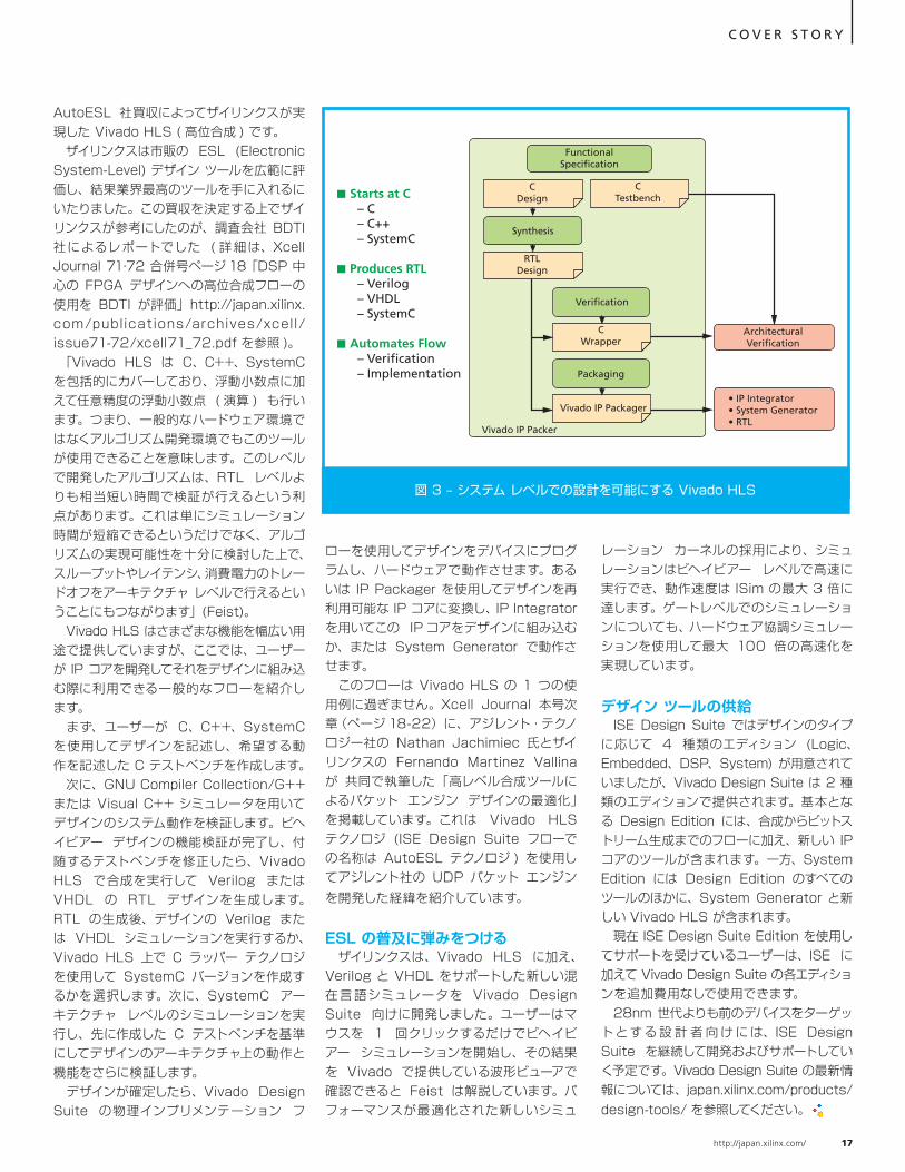
図 3 – システム レベルでの設計を可能にする Vivado HLS
C O V E R S T O R Y
http://japan.xilinx.com/ 17
ギガビット イーサネットは、強化されたトライモード イーサネット MAC (TEMAC) プリミティブが利用可能になったことで、ワークステーションまたはノートブック PC を FPGA ベースのエンベデッド プラットフォームに接続するときに利用できるインターコネクト オプションとして広く利用されています。イーサネット ベースの FPGA デザインの開発で主な障害になるのは、Internet Protocol (IP) スタックの処理にはプロセッサが必要であると知覚されていることです。この問題の解決のため、私たちは、AutoESL 高レベル合成ツールを使用して、高性能な IPv4 User-Datagram Protocol (UDP) パケット転送エンジンを開発しました。 Agilent 社の Measurement Research Lab のデザイン チームは、各種プロトコル (UDP、Address Resolution Protocol (ARP)、および Dynamic Host Configuration Protocol (DHCP)) 間のパケット交換の詳細を規定した Internet Engineering Task Force (IETF) の Request for Comments (RFC) に基づく独自の C ソース コードを作成しました。このデザインでは、ハードウェア パケット処理エンジンをインプリメントする際に CPU を必要としません。このアーキテクチャは、最小限のレイテンシで、回線の通信速度でトラフィックを処理することができ、ロジック リソース エリアにコンパクトにインプリメントが可能です。AutoESL ツールを使用すれば、最小限の労力でユーザー インターフェイスを変更し、1 つ以上の FIFO ストリームまたは複数の RAM インターフェイス ポートに適合させることができます。AutoESL は Xilinx® ISE® Design Suite に新たに追加されたツールであり、新しい Vivado ™ Design Suite では Vivado HLS と呼ばれます
(カバー ストーリー、ページ 12-17 を参照)。
AutoESL ツールによるインファブリック、プロセッサ フリーの UDP ネットワーク パケット エンジンの作成
XCELLENCE IN COMMUNICATIONS
by Nathan Jachimiec, PhDR&D EngineerAgilent Technologies Technology Leadership [email protected]
Fernando Martinez Vallina, PhD Software Applications EngineerXilinx, [email protected]
High-Level Synthesis Tool Delivers Optimized Packet Engine Design
高レベル合成ツールによるパケット エンジン デザインの最適化
18 Xcell Journal 79・80 合併号
IPV4 USER DATAGRAM PROTOCOL 現在のインターネットで支配的なプロトコルは Internet Protocol version 4 (IPv4) で あ り、Internet Protocol version 6 (IPv6) も着実に知名度を拡大しています。 多くの開発者が IP について議論する場合、通常は信頼性と輻輳管理を提供するコネクション ベースのプロトコルである Transmission Control Protocol (TCP) を指します。しかし、ビデオ ストリーミング、テレフォニー、ゲーム、分散センサー ネットワークなどの多くのアプリケーションでは、帯域幅を拡大して遅延を最小限に抑えることのほうが信頼性より重要です。したがって、これらのアプリケーションでは、通常は TCP の代わりに UDP を使用します。 UDP はコネクションレスで、それ自体は信頼性を備えていません。パケットの損失、重複、送信順序の乱れが発生した場合、送信側がそれを知る方法はありません。ユーザー アプリケーションの側で何らかのパケット検査を実行し、エラーを処理する必要があります。この点で UDP は「非信頼性」プロトコルと呼ばれてきましたが、TCP よりも高い性能を提供します。UDP は、IP をサポートするほぼすべての主要オペレーティング システムでサポートされています。高水準ソフトウェア プログラミング言語では、ネット
ワーク ストリームを「ソケット」と呼びますので、UDP はデータグラム ソケットとなります。
センサー ネットワーク アーキテクチャAgilent 社では、Xilinx Virtex®-5 FPGA
とアナログ デジタル コンバーター (ADC) をインターフェイスする LAN ベースのセンサー ネットワークを開発しました。FPGA はデータ アグリゲーションを実行し、要求された数のサンプルを既定の IP アドレス ( すなわち、ホスト PC) にストリーミングします。FPGA のブロック RAM はほぼすべて信号処理に使用されていたため、ソフト プロセッサ用のファームウェアを格納できる十分なメモリがありませんでした。そこで、最小限のネットワーク機能をインプリメントし、UDP によってセンサー データをホストに転送することにしました。高帯域幅と低レイテンシが必要とされたため、UDP パケット ストリーミングが好ましいものとしてネットワーク モードに採用されました。 このデータは遅れが許されないため、失われたサンプル データを再送信するよりも、新しいサンプル データ セットを送信する方が適切です。ここで、私たちは 2 つの重要な課題に直面しました。まず第 1 に、ホスト デバイスの過負荷を避ける必要がありました。つまり、多数のインバウンド サンプルの
効率的な処理方法を見つける必要がありました。第 2 に、次のサンプル セットが内部バッファーからオーバーフローする前に、UDP パケットを迅速にフォーマットし、必要な IP ヘッダー フィールドとオプションの ( 必要な ) UDP ペイロード チェックサムを計算する必要がありました。
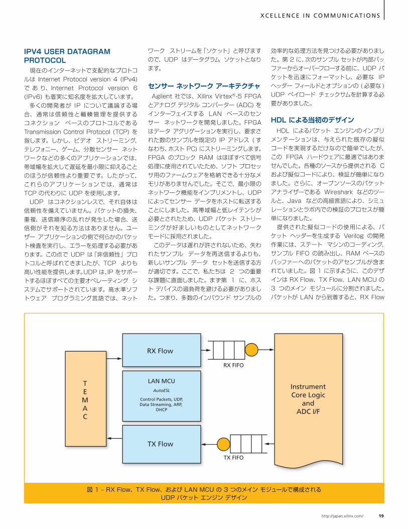
HDL による当初のデザイン HDL によるパケット エンジンのインプリメンテーションは、与えられた既存の擬似コードを実現するだけなので簡単でしたが、この FPGA ハードウェアに最適ではありませんでした。各種のソースから提供される C および擬似コードにより、検証が簡単になりました。さらに、オープンソースのパケット アナライザーである Wireshark などのツールと、Java などの高級言語により、シミュレーションとラボ内での検証のプロセスが簡単になりました。 提供された擬似コードの使用による、パケット ヘッダーを生成する Verilog の開発作業には、ステート マシンのコーディング、サンプル FIFO の読み出し、RAM ベースのバッファーへのパケットのアセンブルが含まれていました。図 1 に示すように、このデザインは RX Flow、TX Flow、LAN MCU の 3 つのメイン モジュールに分割されました。パケットが LAN から到着すると、RX Flow
RX FIFO
InstrumentCore Logic
andADC I/F
TX FIFO
TX Flow
RX Flow
TEMAC
LAN MCU
AutoESL
Control Packets, UDP,Data Streaming, ARP,
DHCP
X C E L L E N C E I N C O M M U N I C AT I O N S
図 1 – RX Flow、TX Flow、および LAN MCU の 3 つのメイン モジュールで構成される UDP パケット エンジン デザイン
http://japan.xilinx.com/ 19
はパケットを検査し、処理のためにインストルメント コアまたは LAN MCU に渡します (ARP または DHCP パケットを処理する場合など )。 TX Flow パケット エンジンは、TX FIFO から N 個の ADC サンプルを読み出し、UDP チェックサムを計算するためにランニング ペイロード チェックサムを計算します。TX FIFO は新しいサンプルが到着するとバッファーに入れ、一方 LAN MCU はこれから送信されるパケットのペイロードを準備します。最後に要求されたサンプルのフェッチ後、LAN MCU は、IP/UDP パケットの残りのヘッダー フィールドを計算します。ネットワーク用語では、この手順を TX チェックサム オフロードと呼びます。 パケット フィールドが生成されると、LAN MCU は TEMAC の送信のためにパケットを TEMAC に送りますが、( 転送先デバイスによる受信ではなく ) TEMAC が送信正常終了の ACK 応答を返すまではパケットを保持します。この最初のパケットが TEMAC による送信を待っているとき、新しいセンサー サンプルが TX FIFO に到着します。最初のパケットの送信が完了すると、パケット エンジンは次のパケットのためにバッファーを解放します。このプロセスは二重バッファー方式で続けられます。次の送信バッファー オーバーフローが 差し迫ってい るときに TEMAC がエラーを報告した場合は、次のサンプル セットの処理を続けられるようにエラー パケットは廃棄され、例外が記録されます。このパケット フォーマットにはサンプル セットのタイムスタンプが組み込まれているため、ホストはサンプル セット内の不連続性を認識し、それに対応します。 パケット送信のレイテンシは、N 個の ADC サンプルの読み出しに必要なサイクル数+パケット ヘッダー フィールド (IPv4 フラグ、ソースおよびデスティネーション アドレス フィールド、UDP 擬似ヘッダー、IP チェックサムおよび UDP チェックサムなど ) の生成に必要なサイクル数になります。チェックサムの計算はやや問題を含んでいます。計算にはパケット全体の読み出しが必要ですが、チェックサムはペイロード バイトよりも前に置かれるためです。
HDL のコーディングの困難さ センサー ネットワークの高帯域幅と低レイテンシの要件に対応するため、必要なサンプル レートを処理できる最適なハード
ウ ェ ア デ ザ イ ン が 必 要 で し た。 当 初 Verilog でインプリメントした直接的な手法では、フロアプランなしでは 125MHz のクロック レートを満たすことができず、IP/UDP パケット ヘッダー フィールドの生成に 17 クロック サイクルかかっていました。当初の HDL デザインの開発時には、TEMAC インターフェイスの 微 妙な特 性の 理 解に ChipScope™ ツールが非常に重要でしたが、このツールは 125MHz クロックの達成という目標を妨げてもいました。追加のロジック キャプチャー回路によってクリティカル パスが変更され、タイミング クロージャのために手作業によるフロアプランが必要になるようです。 HDL による直接的なデザインは 4 オペランド加算器を使用してデザインのさまざまなステートで複数のヘッダー フィールドを合計していたため、クリティカル パスは IP および UDP ヘッダー チェックサムを計算する経路でした。この HDL デザインは、ステート マシンの各サイクルでできるだけ多くの作業を実行しようとする「欲張りな」スケジューリング アルゴリズムを試みていました。これらの操作では ChipScope ツールを取り外し、フロアプランを実行することでタイミング クロージャを達成しました。 HDL によるデザインでは、送信パケット バッファーとして機能する 32 ビット幅のブロック RAM の 1 ポートだけを使用しました。32 ビット幅のメモリを選んだのは、BRAM プリミティブの本来の幅が 32 ビットであり、32 ビット幅のメモリではバイト イネーブル書き込みアクセスが可能なため、送信バッファーに対する読み出し / 変更 / 書き込みアクセスを回避できるからです。 有限ステート マシン (FSM) は、バイト イネーブルを使用して、RAM アドレスでの変更を必要とするヘッダー フィールド バイトに直接書き込みます。しかし、基盤となるザイリンクスのファブリックとアルゴリズムの知識に基づいた適切なデザインの選択肢と思われたものは、最適なデザインをもたらしませんでした。このデザインは、4 入力の加算器を手作業で配置しなければ、タイミング条件を満たせませんでした。 UDP アルゴリズムは、C コードで各種の形式で既に利用可能であるか、IP に関連する RFC ドキュメントに擬似コードとして記述されていたため、UDP パケット エンジンを C で再コーディングすることは主要な作業ではなく、パケット ヘッダーの処理に
ついてより良い知見をもたらすことが証明されました。既存 の 擬 似コードを利用して Verilog の記述を始める手法は、コーディングの迅速化には最適かもしれませんが、関連するデータ フローと制御フローについて十分に理解していなければ、十分なパフォーマンスは得られないでしょう。
AUTOESL の利点 AutoESL による FIFO インターフェイスおよび RAM インターフェイスの抽象化は、パフォーマンスの面から見て非常に有益な最適化機能であることが証明されました。C で直接コーディングできますので、ARP ルーチンと DHCP ルーチンの両方をパケット エンジンに簡単に組み込めるようになりました。このデザインのフローチャートを図 2 に示します。HDL デザインでは、(Verilog コーディングのままの ) デザインのアグリゲーションおよびセンサー インターフェイスに接続される、1 バイト幅の FIFO インターフ ェイ ス を 利 用 し ま し た。 ま た、 こ の Verilog デザインでは、4 バイトのサンプル データを収集し、転送バッファー RAM 内に 32 ビット ワードとして保存する、32 ビット メモリ インターフェイスを利用しました。 AutoESL ツールは、「配列再形成」指示子によってメモリ インターフェイスを最適化し、C コードで 8 ビット メモリとして記述された送信バッファーを 32 ビット メモリに変換しました。これは、ヘッダー フィールドを 32 ビット ワードへ配置しようとするとビット シフトが必要となるため、この指示子の使用により C コードがヘッダー フィールドの多くのビット操作を行わなくて済むことを意味していました。 また、AutoESL ツールは、リトルエンディアンとビッグエンディアンのバイトオーダーの問題も軽減しました。この最適化により、TX オフロード機能がパケット チェックサムを計算してヘッダー フィールドを生成するまでのレイテンシは、当初 Verilog で記述されたときの 17 クロックから 7 クロック サイクルに短縮され、タイミング条件を簡単に満たせるようになりました。AutoESL ツールの現行バージョンは、RAM 書き込み時にバイト イネーブルを操作する機能を持っていませんが、AutoESL ツールの長期的なロードマップにはバイト イネーブル メモリのサポートが含まれています。したがって、AutoESL ツールの効果は将来さらに向上するでしょう。
X C E L L E N C E I N C O M M U N I C AT I O N S
20 Xcell Journal 79・80 合併号
AutoESL ツールではもう 1 つの最適化手法を実行できました。この手法は偶然発見されたもので、ザイリンクスのブロック RAM は基本的にデュアルポートであるため、メモリの両方のポートにアクセスすることが可能でした。Verilog デザインでは、TEMAC へのインターフェイスが送信バッファーにアクセスする際にアービトレーションを不要にするために、送信バッファーの第 2 ポートを未使用にしていました。ザイリンクスの真のデュアルポート RAM 向けの最適化を AutoESL ツールに実行させることで、バッファーの 2 つの異なる位置からの読み出しまたは書き込みを実行できるようになりました。その結果、ヘッダーの生成に必要なサイクル数は実際に 1/2 に減少しました。この場合、AutoESL ツールが取得した未使用のメモリ ポートに TEMAC インターフェイスがアクセスできるように、メモリの第 2 ポート用の簡単なアービターを Verilog で作成する必要がありましたが、その労力に十分見合うだけのレイテンシの削減を実現できました。
送信バッファーとサンプル FIFO インターフェイスのビット幅は、指示子を使用して制御しました。残念なことに、AutoESL ツールは自動的にデザインを最適化しません。設計者がさまざまな指示子で実験し、試行錯誤によって最も効果的な方法を判断する必要があります。このデザインでは、パケット フィールドの処理に必要なクロック サイクル数の削減と 125MHz での動作を目標にしました。 このデザインの最適化においては、「配列再形成」指示子とループ「パイプライン」指示子が重要でした。配列再形成指示子は、RAM と FIFO インターフェイスのビット幅を変更します。これにより、最終的にはクロック サイクルごとに複数のヘッダー フィールドを並列で処理し、メモリに書き戻せるようにします。サイクル数を最小限に抑える最適な組み合わせは、送信バッファーのビット幅 32 でした。ADC サンプルをフィードする FIFO の幅は、全体的なレイテンシの削減には影響を与えません。これは、サンプルの到着を強制的に早めることは不可能なためです。
ループ パイプライン指示子は、FIFO インターフェイスからのプッシュとポップを行うループがバック トゥ バックで動作できることをコンパイラに指示します。この指示子も極めて重要です。パイプライン指示子がない場合、AutoESL ツールは、スケジューリング上の理由で FIFO のポップ間に 3 ~20 クロック サイクルを消費します。したがって、メモリ間でデータをストリーミングするときは、できるだけ多くパイプラインを使用して低レイテンシを達成することが非常に重要です。 ザイリンクスのブロック RAM のデータ出力には、1 ~ 3 クロック サイクルのプログラム可能なレイテンシが伴います。3 サイクルの読み出しレイテンシを確保することで、
「クロックから Q 出力までの」タイミングを最小限に抑えられます。さまざまな読み出しレイテンシで実験することは、RAM プリミティブまたは「コア」リソースの「レイテンシ」指 示 子 を 変 更 す る だ け で 可 能 で す。AutoESL が実行するスケジューリング アルゴリズム上のの理由で、RAM へのアクセス
X C E L L E N C E I N C O M M U N I C AT I O N S
RXInterrupt
DHCPExchange
IdentifyPacket
UDPControl
UDPDHCP
PrepareUDP
Packet
Stream ControlInstruction to Core
ADC Samplesfrom Core
GenerateChecksums
Stream toTEMAC
ARPResponse
ARPRequest
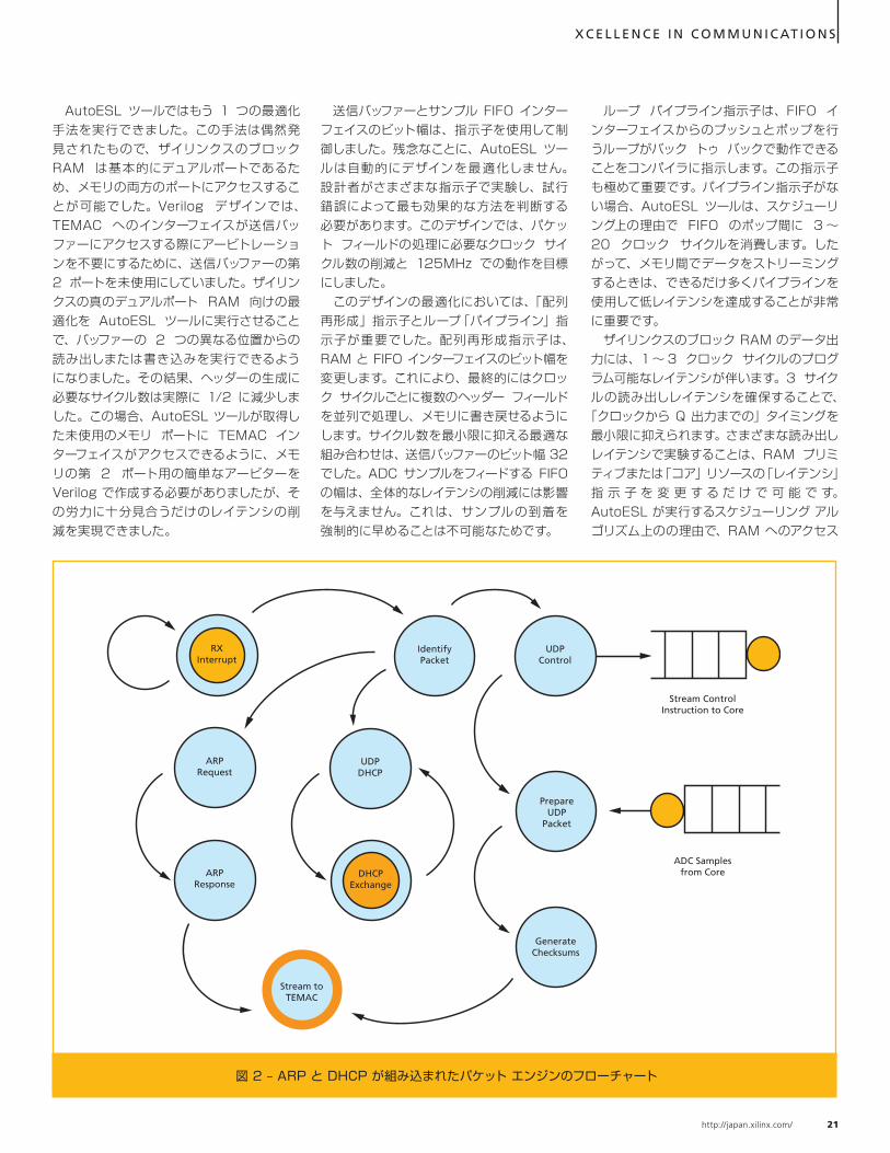
図 2 – ARP と DHCP が組み込まれたパケット エンジンのフローチャート
http://japan.xilinx.com/ 21
に 3 サイクルの読み出しレイテンシを追加しても、全体的なパケット ヘッダー生成のレイテンシは 1 サイクル増えただけです。メモリ レイテンシのサイクルの追加により、デザインに余裕が生まれ、配置配線の作業が容易になりました。 また、AutoESL デザインには ARP ルーチンと DHCP ルーチンをインプリメントしました。これらのルーチンを Verilog でコーディングするには大きな労力が必要なため、それまでこの作業を避けていました。難しくないとは言え、ARP と DHCP を Verilog で記述するには極めて手間がかかり、実行するのに多数のステートを必要とします。たとえば、ARP の要求と応答のやり取りには 70 以上のステートが必要です。Verilog FSM にコーディング エラーが 1 箇所でもあると、解決するのに数日かかることがあります。この理由だけで、多くの設計者は、CPU を使用してこれらのネットワーク ルーチンを実行する方を好みます。 全体的に、AutoESL ツールは、UDP パケット エンジンの合成可能なネットリスト の 生 成 に 優 れ た 成 果 を 上 げ まし た。AutoESL ツールが生成したモジュールは、既存の 2 つの ADC インターフェイス モジュールと TEMAC インターフェイス モジュールの間にフィットし、必要なパケット ヘッダー生成タスクとその他のタスクを実行しました。私たちは、AutoESL ツールが作成したデザインをコア デザインに統合し、Mentor Graphics 社の ModelSim でシミュレーションして機能検証を実行しました。無駄のないデザインにより、当初の HDL デザインよりも少ない労力で合成、マップ、および配置配線を行い、タイミン
グ クロージャに到達できました。しかも、ARP と DHCP のサポートなど、機能は大幅に増えています。 Verilog による当初のデザインと、「LAN MCU」および「TX Flow」モジュールの作成に AutoESL を利用したハイブリッド デザインを比較した結果は印象的です。ルックアップ テーブル (LUT) の使用率の比較を表 1 に示します。HDL バージョンの TX Flow では 37% 以上少なくなっていますが、AutoESL デザインはより多くの機能を組み込んでいます。最も印象的なのは、AutoESL ツールにより、パケット ヘッダーの生成に必要なサイクル数が 59% も減ったことです。「TX オフロード」アルゴリズムのレイテンシを表 2 に示します。 HDL デザインのクリティカル パスは UDP チェックサムを計算する経路でした。このデザインと AutoESL デザインを比較した結果、HDL デザインでは 10 レベルのロジック回路と 6.4ns のトータル パス遅延が発生したのに対して、AutoESL デザインでは 3 レベルのロジック回路と 3.5ns のトータル パス遅延に最適化されたことがわかりました。HDL デザインの開発には、約 1 カ月にわたる作業を必要としました。AutoESL デザインにもほぼ同じ期間をかけて、AutoESL ツールの細かい使い方に慣れながら、より多くの機能を組み込みました。
レイテンシとスループット HDL デザインに対する AutoESL デザインの大きなメリットは、制御分析とデータ フロー分析を実行して、この情報に基づいて演算の順序を変更し、レイテンシを最小限に抑えてスループットを増加させる点にあります。
X C E L L E N C E I N C O M M U N I C AT I O N S
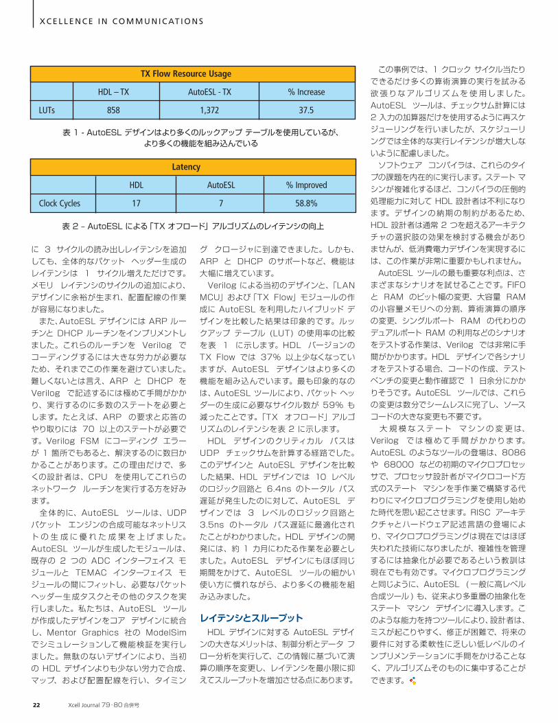
TX Flow Resource Usage
HDL – TX AutoESL - TX % Increase
LUTs 858 1,372 37.5
表 1 - AutoESL デザインはより多くのルックアップ テーブルを使用しているが、より多くの機能を組み込んでいる
Latency
HDL AutoESL % Improved
Clock Cycles 17 7 58.8%
表 2 – AutoESL による「TX オフロード」アルゴリズムのレイテンシの向上
この事例では、1 クロック サイクル当たりできるだけ多くの算術演算の実行を試みる欲 張りな アルゴリズ ムを 使 用しました。AutoESL ツールは、チェックサム計算には 2 入力の加算器だけを使用するように再スケジューリングを行いましたが、スケジューリングでは全体的な実行レイテンシが増大しないように配慮しました。 ソフトウェア コンパイラは、これらのタイプの課題を内在的に実行します。ステート マシンが複雑化するほど、コンパイラの圧倒的処理能力に対して HDL 設計者は不利になります。デザインの納期の制約があるため、HDL 設計者は通常 2 つを超えるアーキテクチャの選択肢の効果を検討する機会がありませんが、低消費電力デザインを実現するには、この作業が非常に重要かもしれません。 AutoESL ツールの最も重要な利点は、さまざまなシナリオを試せることです。FIFO と RAM のビット幅の変更、大容量 RAM の小容量メモリへの分割、算術演算の順序の変更、シングルポート RAM の代わりのデュアルポート RAM の利用などのシナリオをテストする作業は、Verilog では非常に手間がかかります。HDL デザインで各シナリオをテストする場合、コードの作成、テストベンチの変更と動作確認で 1 日余分にかかりそうです。AutoESL ツールでは、これらの変更は数分でシームレスに完了し、ソース コードの大きな変更も不要です。 大 規 模 な ステ ート マシン の 変 更 は、Verilog で は 極 めて 手 間 が かかりま す。AutoESL のようなツールの登場は、8086 や 68000 などの初期のマイクロプロセッサで、プロセッサ設計者がマイクロコード方式のステート マシンを手作業で構築する代わりにマイクロプログラミングを使用し始めた時代を思い起こさせます。RISC アーキテクチャとハードウェア記述言語の登場により、マイクロプログラミングは現在ではほぼ失われた技術になりましたが、複雑性を管理するには抽象化が必要であるという教訓は現在でも有効です。マイクロプログラミングと同じように、AutoESL ( 一般に高レベル合成ツール ) も、従来より多重層の抽象化をステート マシン デザインに導入します。このような能力を持つツールにより、設計者は、ミスが起こりやすく、修正が困難で、将来の要件に対する柔軟性に乏しい低レベルのインプリメンテーションに手間をかけることなく、アルゴリズムそのものに集中することができます。
22 Xcell Journal 79・80 合併号
XCELLENCE IN SOLID-STATE DISKS
Xilinx 7 シリーズ デバイスが PCI Express ソリッド ステート ディスク (SSD)デザインの速度と性能を向上
Designing a 19-nm Flash PCIe SSD with Kintex-7 FPGAs
by Yilei WangSenior Hardware Engineer
Memblaze China
Xiangfeng LuCTO
Memblaze China
Kintex-7 FPGA を使用した 19nm フラッシュ PCIe SSD の設計
http://japan.xilinx.com/ 23
NAND フラッシュ メモリを採用したソリッド ステート ディスク (SSD) テクノロジは、メカニカル ドライブを使用した従来のストレージ システムに比べて低い消費電力で高いスループットを提供します。このため、過去 10 年間に SSD の利用はハンドヘルド機器からノートブック PC/ デスクトップ PC へと急速に広がり、現在ではエンタープライズ ストレージ市場へも浸透しています。エンタープライズ ストレージ業界が Serial Advanced Technology Attachment (SATA) 規格に準拠した SSD を採用したことで、普及のペースはさらに加速しています。 SSD メーカー各社は、19nm プロセス技術のフラッシュ メモリを使用して新たなレベルの性能と集積度を達成する次世代システムを構想していますが、SATA 規格はこの構想に追随していません。最新バージョンの SATA 3.0 でも、6Gbps の物理インターフェイスでは SSD の NAND フラッシュ アレイの最高スループットに対応できないため、ドライブの性能向上が足踏みしています。 インターフェイスのボトルネックを解消する PCI Express® SSD は、市場に大きな衝撃を与えています。PCIe® は、SATA よりも性能と拡張性に優れたローカル バスの業界標準規格です。PCIe は 1 ~ 16 レーンをサポートするマルチレーン高速シリアル リンクに基づ いており、各レーンは最 大 8Gbps (Gen1 では 2.5Gbps、Gen2 で
は 5Gbps、Gen3 では 8Gbps) で動作します。SSD 向けの PCIe インターフェイスは、ギガバイト レベルのスループットとマージンの向上を可能にし、予測しうる将来における NAND フラッシュ テクノロジの進化に対応します。 ただし、19nm フラッシュを採用した PCIe ベースの SSD システムの開発は簡単ではありません。PCIe インターフェイスには、SATA よりも高速なシリアル リンクと複雑なインターコネクトが必要です。スループットの要求に応えるためには、PCIe ダイレクト メモリ アクセス (DMA) がギガバイト レベルの帯域幅で動作する必要があります。さらに、19nm プロセスを採用したノードでは、フラッシュの信頼性、すなわち厳密には「摩耗 (wear)」と呼ばれる測定基準 (NAND にエラーが発生するまでの読み出しまたは書き込み回数 ) が大きな問題となります。19nm プロセスのフラッシュを採用する場合は、ウェアレベリングとエラー訂正を従来より高速に実行する必要があります。 Xilinx® Kintex ™ -7 FPGA は、旧世代の FPGA の 2 分の 1 以下の価格で、ハイエンド FPGA の新たな性能基準を確立します。Kintex-7 ファミリは、ザイリンクスが TSMC 社の HPL ( 高性能、低消費電力 ) 28nm プロセスを駆使して開発した 4 つの製品ラインの 1 つであり、電力効率を最大限に高めて、旧世代の FPGA の 50% と少
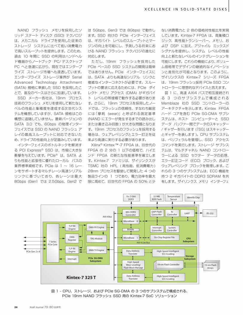
ない消費電力と 2 倍の価格対性能比を実現しています。Kintex-7 FPGA は、高集積ロジック、高性能トランシーバー、メモリ、および DSP に加え、アジャイル ミックスド シグナルを提供し、システム レベルの性能向上と新たなレベルのインテグレーションを可能にします。これらの機能により、ボリューム価格帯でデザインの継続的なイノベーションと差別化が可能となります。このように、ザイリンクスの Kintex-7 シリーズ FPGA は、19nm フラッシュ採用 PCIe SSD コントローラーに理想的なデバイスと言えます。 図 1 に、高速 AXI4 バスで相互接続される 3 つ の サ ブ シス テムで 構 成 さ れ る Memblaze 社の SSD コントローラーのアーキテクチャを示します。Kintex FPGA ハード コアを含む PCIe SG-DMA サブシステムは、ホスト コンピューターと SSD データ バッファー間でデータのスキャッター/ ギャザーを行います (「SG」はスキャッターとギャザーを表します )。CPU サブシステムは、ペリフェラルを管理し、SSD アクセス コマンドを実行します。ストレージ サブシステムは、マルチチャネル NAND コントローラーによる SSD セクター データの処理、エラー訂正コード (ECC) ブロック、およびウェアレベリング ブロックを管理します。これらの 3 つのサブシステムは、ECC 機能を持つ 2 ギガバイトの DDR3 SDRAM を共有します。ザイリンクス メモリ インターフェ
X C E L L E N C E I N S O L I D - S T A T E D I S K S
PCIe Gen 2 x 8
7 SeriesPCIe Core
TLP RXEngine
DMARegister
TLP RXEngine
Interrupt
DMA RX Engine
TAG Module
DMA TX Engine
PCIe SG-DMASubsystem
Kintex-7 325 T
AXI 4 Bus
AXI 4 Lite Bus
9 x 2 GbitDDR3
32-MB XOR Flash
TemperatureSensor
Identify Chip
MIG DDR3Controller
MicroBlaze 0
MicroBlaze 1
BRAMs
Data AddressTranslate
High-Speed Wear Leveling/
Flash Block Manage
Data AddressTranslate
QSPI FlashController
IIcController UART RS-232
InterruptController
SystemController
On-Chip Register File CPUSubsystem
High-Speed Intelligent ECC Ecoding
High-Speed Intelligent ECC Ecoding
Storage Subsystem
19-nm Flash Controller 19-nm FlashArrays
図 1 – CPU、ストレージ、および PCIe SG-DMA の 3 つのサブシステムで構成される、PCIe 19nm NAND フラッシュ SSD 用の Kintex-7 SoC ソリューション
24 Xcell Journal 79・80 合併号
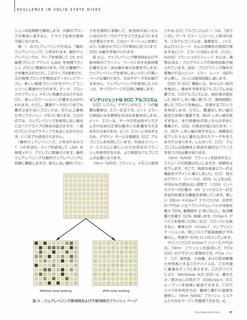
SG-DMA コアの主な機能は、ホストから送信される TLP パケットを処理し、それに応答することです。SG-DMA は、ホスト メモリに対する PCIe マスター アクセスとして機能し、ホストとローカル メモリ間でデータを転送します。ホストは DMA コントローラーにコマンドを送信し、DMA アクセスを制御します。コマンド コードは、特定のホスト TLP レジスタ書き込みのデータ内に埋め込まれます。SG-DMA コントローラーは、ホストの読み出しコマンドに応答して、ローカル メモリからホスト メモリへデータ
を転送する SG-DMA 書き込み要求を開始します。同様に SG-DMA コントローラーは、ホストの書き込みコマンドに対して、ホスト メモリからローカル メモリへデータを転送する DMA 読み出し要求を開始します。図 3 にこの処理フローを示します。
AXI4 インターコネクト AXI インターコネクト IP は、1 つ以上の AXI メモリ マップ方式マスター デバイスと 1 つ以上のメモリ マップ方式スレーブ デバイスを接続します。AXI インターフェイスは、ARM の AMBA® AXI 仕様のバージョン 4 に準拠しています。この仕様には、AXI4-Lite 制御レジスタ インターフェイスのサブセットも含まれます。このインターコネクト IP は、メモリ マップ方式の転送のみを前提にしているため、AXI4-Stream による転送には適用できません。AXI インターコネクト
イス ジェネレーター (MIG) ツールを使用すれば、ECC DDR3 SDRAM コントローラーを簡単に生成できます。 このデザインでは、7 シリーズ PCIe ハード コアによって物理 /TLP 層がインプリメントされ、デザインは高性能 PCIe エンドポイントとして最小限のレイテンシで動作します。新しいエンベデッド MircoBlaze® コアと ARM® AXI4 インターコネクトにより、オンチップ バスのボトルネックは完全に解消されます。DDR3 ハード コアはディスク キャッシュに対して 51.2Gbps ECC ソ
リューションを提供します。一方、低消費電力のロジック リソースにより、高性能のウェアレベリングとインテリジェントな ECC アルゴリズムを簡単に実行できます。さらに、豊富な高性能 I/O リソースにより、19nm NAND フラッシュ アレイへのインターコネクトも簡単に行えます。
PCI Express SG-DMA このデザインでは、PCIe インターフェイスに、ホストとローカル AXI4 バス間の高速通信をサポートする高速 DMA コントローラーが必要でした。SSD フラッシュ アレイのスループットは、最大 2.5GBytes/s に達することができます。PCIe インターフェイスのデザインを簡略化し、フラッシュ チップの進化とともにマージンを拡大できるように、8 レーンの PCIe Gen2/Gen3 アーキテクチャを採用しました。
X C E L L E N C E I N S O L I D - S T A T E D I S K S
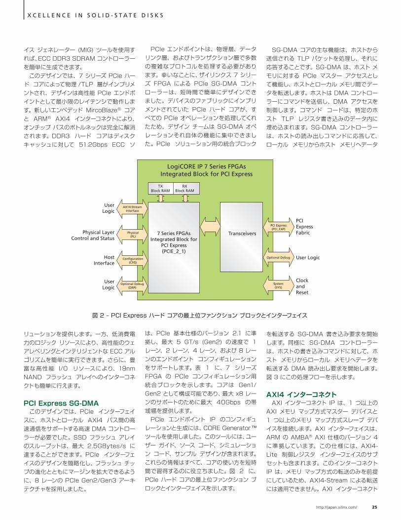
PCIe エンドポイントは、物理層、データリンク層、およびトランザクション層で多数の複雑なプロトコルを処理する必要があります。幸いなことに、ザイリンクス 7 シリーズ FPGA による PCIe SG-DMA コントローラーは、短時間で簡単にデザインできました。デバイスのファブリックにインプリメントされていた PCIe ハード コアが、すべての PCIe オペレーションを処理してくれたため、デザイン チームは SG-DMA オペレーションそれ自体の機能に集中できました。PCIe ソリューション用の統合ブロック
は、PCIe 基本仕様のバージョン 2.1 に準拠し、最大 5 GT/s (Gen2) の速度で 1 レーン、2 レーン、4 レーン、および 8 レーンのエンドポイント コンフィギュレーションをサポートします。表 1 に、7 シリーズ FPGA の PCIe コンフィギュレーション用統合ブロックを示します。コアは Gen1/Gen2 として構成可能であり、最大 x8 レーンのサポートのために最大 40Gbps の帯域幅を提供します。 PCIe エンドポイント IP のコンフィギュレーションと生成には、CORE Generator ™ ツールを使用しました。このツールには、ユーザー ガイド、ソース コード、シミュレーション コード、サンプル デザインが含まれます。これらの情報はすべて、コアの使い方を短時間で習得するのに役立ちました。図 2 に、PCIe ハード コアの最上位ファンクション ブロックとインターフェイスを示します。
LogiCORE IP 7 Series FPGAsIntegrated Block for PCI Express
UserLogic
Physical LayerControl and Status
HostInterface
UserLogic
7 Series FPGAsIntegrated Block for
PCI Express(PCIE_2_1)
Transceivers
PCIExpressFabric
User Logic
ClockandReset
PCI Express(PCI_EXP)
Optional Debug
System(SYS)
TXBlock RAM
RXBlock RAM
AX14-StreamInterface
Physical(PL)
Configuration(CFG)
Optional Debug(DRP)
図 2 – PCI Express ハード コアの最上位ファンクション ブロックとインターフェイス
http://japan.xilinx.com/ 25
X C E L L E N C E I N S O L I D - S T A T E D I S K S
IP は、ザイリンクスのエンベデッド開発ツール キット (EDK) からの pCORE として、またはザイリンクス CORE Generator IP カタログからのスタンドアロン コアとして使用できます。 設計者はザイリンクス AXI4 IP がサポートする 2 つの動作モードを選択できます。パフォーマンスを最 適化するクロスバー モードでは、書き込みチャネルと読み出しチャネル用の並列パスウェイを備えた共有アドレス複数データ (SAMD) クロスバー アーキテクチャを使用します。エリアを最適化する共有アクセス モードでは、共有書き込みデータ、共有読み出しデータ、および 1 つの共有アドレス パスウェイを考慮しています。2 つ の モ ードは、インクリメンタル (INCR) バーストの場合、最大バースト長は 256、可変データ幅は 32 ビットから最大
1,024 ビットです。伝播 USER 信号が存在する場合、それを各チャネルがサポートします。この場合、USER 信号幅はチャネルごとに独立して設定可能です ( オプション )。 AXI4 イ ン タ ー コ ネ ク ト は、PCIe SG-DMA と DDR3 メモリ間の高性能な接続をサポートします。また AXI4-Lite 共有バスも、ロジック リソースの消費が最小限で済む、低速オンチップ インターコネクトに最適なソリューションであることがわかりました。
ウェアレベリング テクノロジ ウェアレベリングとは、ソリッド ステート ドライブのフラッシュ メモリなど、各種の消去可能なコンピューター ストレージの寿命の延長を目的としてストレージ メディア メーカー各社が利用する設計手法です。フラッシュ メモリ システムに使用されるウェ
アレベリング メカニズムはいくつかあり、寿命がどの程度延長されるかは方式ごとに異なります。 ウェアレベリングを使用しないフラッシュ メモリ ストレージ システムは、フラッシュへのデータの書き込み寿命はそれほど長くありません。ウェアレベリングを使用しない場合、フラッシュ コントローラーは、オペレーティング システム (OS) から論理アドレスをフラッシュ メモリの物理アドレスに永続的に割り当てる必要があります。つまり、既に書き込み済みのブロックに対して書き込みを行うたびに、まず同じロケーションの読み出し、消去、変更、再書き込みを行うことになります。この操作には非常に時間がかかります。また、フラッシュ上のほかのロケーションがまったく使用されていなくても、頻繁に書き込まれるロケー
Receive TLP register access TLP write?
DMA command?
DMA write?
Send TLP write requestwith write data to host
Await TLP DMA completionwith read data from host
Send TLP register completewith register value
Send TLP read request
Set register with TLP value
PCIe
Gen (Integrated block)*
Artix-7 Kintex-7 Virtex-7 T Virtex-7 XT Virtex-7 HT
Gen2 Gen2 Gen2 Gen3 Gen3
x4 x8 x8 x8 x8
1 1 3-4 2-4 1-3
5 5 8 8 8
Width
Number of Blocks
Serial Date Rate (Gbps)
*Based on symmetric filter implementation
表 1 – PCI Express 用の各種 7 シリーズ FPGA の統合ブロック
図 3 – SG-DMA コントローラーの動作
26 Xcell Journal 79・80 合併号
される ECC アルゴリズムの 1 つは、「非ランダム データ エラー レコード」と呼ばれます。このアルゴリズムは、温度変化、ノイズ、およびストレージ セルの信頼性が原因で発生するビット エラーに対応します。さらに、NAND フラッシュのストレージ セルは、通常は消去 / プログラミングの耐用回数が限られています。消去 / プログラミング操作が累積されるとビット エラー レート (BER) が上昇し、ついには耐用回数に達します。 SSD の ECC 機能には、各セルの BER を検出し、寿命を予測するアルゴリズムが必要です。このアルゴリズムは、設計者が設定した BER しきい値に基づいて、耐用回数に達したブロックを検出し、交換するブロックを特定します。ただし、最適なしきい値の設定が非常に重要です。BER しきい値が低すぎると、まだ信頼性の高いセルが早めに廃棄され、SSD の寿命が短くなります。一方、BER しきい値が高すぎると、信頼性の低下したセルに書き込まれたデータを失うおそれがあります。したがって、ECC アルゴリズムは信頼性と寿命の適切なバランスを見つける必要があります。 19nm NAND フラッシュを採用すると、ストレージの密度は向上しますが、信頼性は低下します。そこで、高度な高速エラー訂正機能をデザインに導入しました。ECC 部分はデザイン リソースの 35% 以上を占め、4GByte の読み出し速度で 1,024 ビット セクター内の最大 49 ビットのエラー訂正を並列処理する機能を実現しています。新しい 28nm Kintex-7 テクノロジは、旧世代の FPGA に比べてシステムレベルの性能を最大 50%、集積度を 2 倍に向上し、総消費電力を最大 50% 削減します。Virtex-5 デバイスを使用した同じ ECC ブロックと比較すると、筆者らの Kintex-7 インプリメンテーションは、同じコストで実装面積が 5% 縮小し、性能が 40% 以上向上しています。 ザイリンクスの Kintex-7 シリーズ FPGA は、19nm フラッシュを採用した PCIe SSD のデザインに理想的です。PCIe ハード コア、高性能、大容量、および低消費電力を特長とするこのデバイスは、この市場に最適なチップと言えます。このデバイスにより、Memblaze 社の SSD は、書き込み / 読み出しの両方で 2GBytes/s のスループットを容易に維持できます。このデバイスを利用すれば、顧客に優れた価値を提供し、19nm NAND フラッシュ システムで大きなマージンを確保できます。
ションは短期間で摩耗します。少数のブロックが寿命に達すると、ドライブ全体が使用不能になります。 第 1 のウェアレベリング方式は、「動的ウェアレベリング」と呼ばれます。動的ウェアレベリングは、マップを使用して OS から論理ブロック アドレス (LBA) を物理フラッシュ メモリに関連付けます。OS が置換データを書き込むたびに、このマップは更新され、元の物理ブロックを無効なデータとしてマークし、新しい物理ブロックがそのマップ エントリーに関連付けられます。データ ブロックがフラッシュ メモリに再書き込みされるたびに、新しいロケーションへの書き込みが行われます。ただし、置換データがいつまでも書き込まれないブロックは、それ以上摩耗せずにフラッシュ メモリに残ります。この方式では、ウェアレベリングを使用しない場合に比べてドライブの寿命は延びますが、一部のブロックはアクティブであるにもかかわらず、いつまでも使用されません。 「静的ウェアレベリング」と呼ばれるもう 1 つの手法も、マップを使用して LBA を物理メモリ アドレスに関連付けます。静的ウェアレベリングは動的ウェアレベリングと同様に機能しますが、変化しない静的ブロッ
X C E L L E N C E I N S O L I D - S T A T E D I S K S
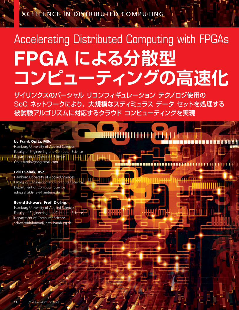
クを定期的に移動して、使用率の低いセルにほかのデータがアクセスできるようにする点が異なります。このローテーション効果により、大部分のブロックが寿命に近づくまで、SSD は動作を続けられます。 図 4 に、ウェアレベリング使用時および不使用時のフラッシュ ページに対する長時間の書き込み / 消去操作後の状態を示します。ウェアレベリングを使用しないメモリの黒いページは壊れており、もはやデータを記録できません。ウェアレベリングを使用したメモリは、すべてのページが正常に機能します。
インテリジェントな ECC アルゴリズム SSD システム デザインのもう 1 つの重要な要素は、エラー訂正です。ビット エラーの原因となる異常な状況は多数存在します。ビット エラーは、データの完全性やシステムそれ自体の正常な動作にも影響を与えるおそれがあります。ビット エラーに対処するため、デザイン チームは複雑な ECC アルゴリズムを利用しています。今回はストレージ システムに新しい小さな形状のフラッシュを使用するため、より高度なアルゴリズムが必要になります。 19nm NAND フラッシュ メモリに使用
Without wear leveling With wear leveling
図 4 – ウェアレベリング使用時および不使用時のフラッシュ ページ
http://japan.xilinx.com/ 27
XCELLENCE IN DISTRIBUTED COMPUTING
by Frank Opitz, MScHamburg University of Applied Sciences
Faculty of Engineering and Computer Science
Department of Computer Science
Edris Sahak, BScHamburg University of Applied Sciences
Faculty of Engineering and Computer Science
Department of Computer Science
Bernd Schwarz, Prof. Dr.-Ing.Hamburg University of Applied Sciences
Faculty of Engineering and Computer Science
Department of Computer Science
ザイリンクスのパーシャル リコンフィギュレーション テクノロジ使用の SoC ネットワークにより、大規模なスティミュラス データ セットを処理する被試験アルゴリズムに対応するクラウド コンピューティングを実現
Accelerating Distributed Computing with FPGAs
FPGA による分散型コンピューティングの高速化
28 Xcell Journal 79・80 合併号
各大学や企業は、ますます複雑化する科学技術アルゴリズムに取り組むために、より高速で消費電力の大きいスーパーコンピューターをインストールするよりも、分散型プラットフォームを利用するようになりました。このプラットフォーム上では、SETI@home などのプロジェクトが数千台のパーソナル コンピューターを使用してデータを計算しています。[1, 2] 現在の分散型コンピューティング ネットワークは、通常は CPU または GPU を使用してプロジェクト データを計算します。 COPACOBANA などのプロジェクトでは、FPGA も利用されています。このプロジェクトは、120 個の Xilinx® FPGA を使用して、DES で暗号化されたファイルを総当たり処理で解読するものです。[3] ただしこの場合、FPGA はすべて 1 箇所に集められるため、コストが高くなり、規模の小さい大学や企業の予算では採用が難しいようです。FPGA を使用して分散型コンピューティングを実現するには、PC を利用して FPGA 全体を継続的に新しいビットストリームでリコンフィギュレーションする必要があるため、これまで FPGA は分散型コンピューティングのユーティリティとして注目されていませんでした。しかし現在では、ザイリンクスのパーシャル リコンフィギュレーション テクノロジを応用することで、分散型コンピューティング ネットワーク用の FPGA ベースのクライ
アントのデザインが可能です。 ハンブルク応用科学大学の筆者らのチームは、こうしたクライアント向けのプロトタイプを作成し、ワンチップ の FPGA にインプリメントしました。筆者らは、静的部分と動的部分の 2 つのセクションで構成されるデザインを構築しました。静的部分は FPGA の起動時にロードされ、動的部分は静的部分にインプリメントされたプロセッサによってネットワーク サーバーからダウンロードされます。動的部分は、共有 FPGA リソースを提供するパーシャル リコンフィギュレーション領域です。[4] このコンフィギュレーションにより、世界のどこにでも FPGA を配置できるため、コンピューティング プロジェクトは低予算で大量の計算能力を利用できるようになります。
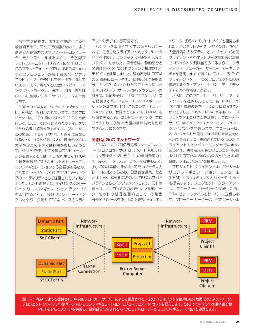
分散型 SoC ネットワーク FPGA は、並列信号処理リソースにより、マイクロプロセッサの 8 分の 1 の低いクロック周波数と 8 分の 1 の低消費電力で 4 倍のデータ スループットを提供します。[5] この計算能力を活用して高いデータ入力レートに対応するため、設計者は通常、たとえば DES 暗号化などのアルゴリズムをパイプラインとしてインプリメントします。[3] 筆者らは、アルゴリズムの高速化と大規模データ セット の 処 理 を目的として、分 散 型 FPGA リソースを使用した分散型 SoC ネッ
トワーク (DSN) のプロトタイプを開発しました。このネットワーク デザインは、すべての登録済みのシステム オン チップ (SoC) クライアントを各ネットワーク参加者の演算プロジェクトに割り当てられるように、クライアント ブローカー サーバー アーキテクチャを適用します ( 図 1)。これは、各 SoC クライアントを 1 つのプロジェクトにのみ接続するクライアント サーバー アーキテクチャでは不可能なことです。 さらに、このブローカー サーバー アーキテクチャを選択したことで、各 FPGA の TCP/IP 接続の数を 1 つだけに減らすことができました。DSN FPGA は専用のデータ セットでアルゴリズムを計算し、ブローカー サーバーは SoC クライアントとプロジェクト クライアントを管理します。ブローカーは、各プロジェクトが同時にほぼ同じ計算能力を利用できるように、接続されている SoC クライアントのスケジューリングを行います。あるいは、演算要求を持つプロジェクトの数よりも利用可能な SoC の数の方が少ない場合は、タイム スライスを使用します。 プロジェクト クライアントは、パーシャル リコン フィギュレ ー ション モ ジュール (PRM) とスティミュラス入力データ セットを提供します。プロジェクト クライアントは、ブローカー サーバーに接続した後、PRM ビット ファイルをサーバーに送信します。ブローカー サーバーは、空きパーシャル
X C E L L E N C E I N D I S T R I B U T E D C O M P U T I N G
Dynamic Part
Static Part
SoC Client 1
Dynamic Part
Static Part
SoC Client n
NetworkInfrastructure
TCP/IPConnection
Broker-ServerComputer
SoC 1
PRM
Data
ProjectClient 1
PRM
Data
ProjectClient m
SoC n
Project 1
Project m
NetworkInfrastructure
Accelerating Distributed Computing with FPGAs
図 1 – FPGA によって提供され、中央のブローカー サーバーによって管理される、SoC クライアントを使用した分散型 SoC ネットワーク。プロジェクト クライアントはパーシャル リコンフィギュレーション モジュールとデータ セットを配布します。SoC クライアントの動的部分は
PRR を介してリソースを供給し、静的部分に含まれるマイクロコントローラーがリコンフィギュレーションを処理します。
http://japan.xilinx.com/ 29
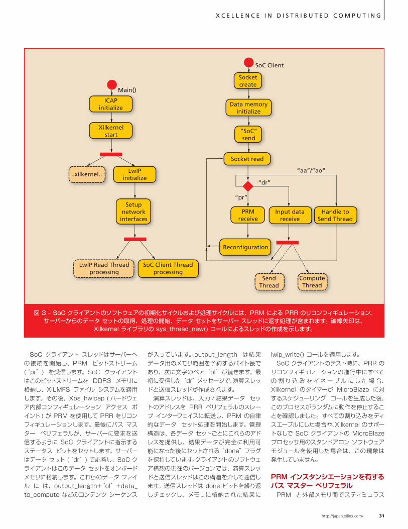
ポートなしでデータ要求を送受信する、コンフィギュレーションが容易な IP を利用することができ、1 ワードの転送当たりのクロック サイクル数を大幅に削減しました。 クライ ア ント / サ ーバー 通 信 用 に は、FPGA の内部ハード イーサネット IP が、プロセッサ システムの静的部分のペリフェラルとして 不 可欠 で す。ローカルリンク TEMAC からメモリ コントローラーへの Soft Direct Memory Access (SDMA) により、データとビット ファイルの転送による PLB への負荷が小さくなります。1,518 バイトのフレームの受信後、SDMA は割り込み要求を生成します。これで lwip_read() 関数はブロック解除され、このデータを処理できます。lwip_write() 関数は、TX チャネルを介して TEMAC に対する DMA 転送を実行するように SDMA に指示します。 SoC クライアントのソフトウェアの基礎となるリアルタイム オペレーティング システムとして、ザイリンクス エンベデッド プロセッサ用カーネルである Xilkernel をインプリメントしました。その目的は、TCP/IP サーバー接続のために、ソケット モードを持つ Lightweight TCP/IP (LwIP) スタック ライブラリを利用することです。図 3 にクライアントのスレッドの初期化、作成、送信、および処理のシーケンスの概要を示します。
リコンフィギャラブル領域 (PRR) を持つ SoC クライアントにこれらのファイルを配布します。SoC クライアントの静的部分 (MicroBlaze™ ベースのマイクロコントローラー ) は、受信した PRM を使用して PRR を動的にリコンフィギュレーションします。 次のステップで、プロジェクト クライアントはデータ セットの送信を開始し、ブローカー サーバーを介して SoC クライアントから計算済みの応答を受信します。プロジェクト クライアントは、演算目的に応じて各種の計算済みデータ セットを比較または評価します。
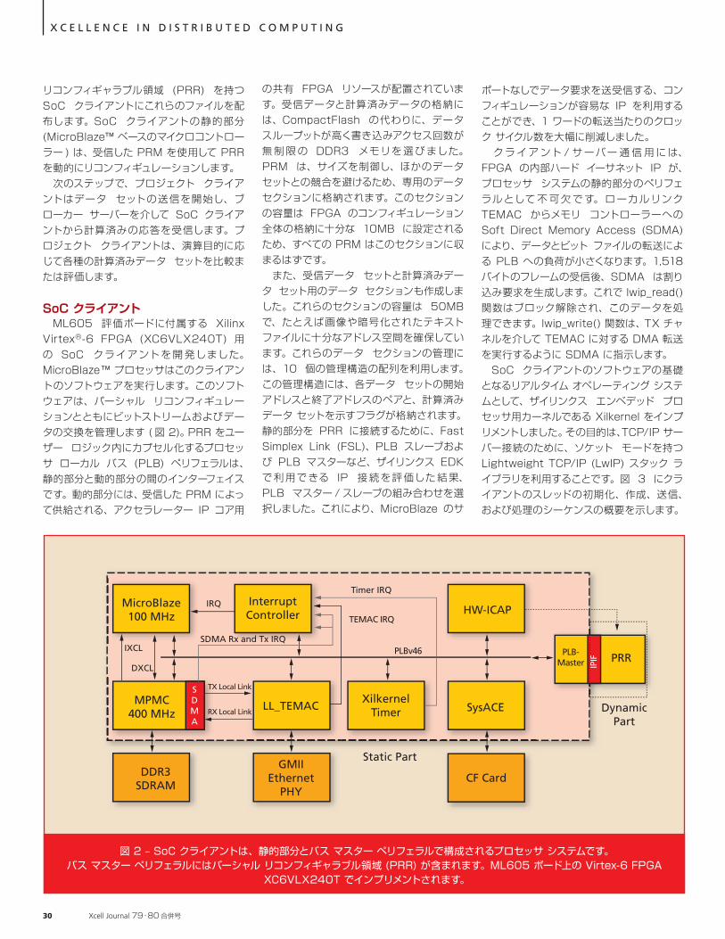
SoC クライアント ML605 評価ボードに付属する Xilinx Virtex®-6 FPGA (XC6VLX240T) 用の SoC クライアントを 開 発しました。MicroBlaze™ プロセッサはこのクライアントのソフトウェアを実行します。このソフトウェアは、パーシャル リコンフィギュレーションとともにビットストリームおよびデータの交換を管理します ( 図 2)。PRR をユーザー ロジック内にカプセル化するプロセッサ ローカル バス (PLB) ペリフェラルは、静的部分と動的部分の間のインターフェイスです。動的部分には、受信した PRM によって供給される、アクセラレーター IP コア用
X C E L L E N C E I N D I S T R I B U T E D C O M P U T I N G
の共有 FPGA リソースが配置されています。受信データと計算済みデータの格納には、CompactFlash の代わりに、データ スループットが高く書き込みアクセス回数が無 制 限 の DDR3 メモリを 選びました。PRM は、サイズを制御し、ほかのデータ セットとの競合を避けるため、専用のデータ セクションに格納されます。このセクションの容量は FPGA のコンフィギュレーション全体の格納に十分な 10MB に設定されるため、すべての PRM はこのセクションに収まるはずです。 また、受信データ セットと計算済みデータ セット用のデータ セクションも作成しました。これらのセクションの容量は 50MB で、たとえば画像や暗号化されたテキスト ファイルに十分なアドレス空間を確保しています。これらのデータ セクションの管理には、10 個の管理構造の配列を利用します。この管理構造には、各データ セットの開始アドレスと終了アドレスのペアと、計算済みデータ セットを示すフラグが格納されます。静的部分を PRR に接続するために、Fast Simplex Link (FSL)、PLB スレーブおよび PLB マスターなど、ザイリンクス EDK で利用できる IP 接続を評価した結果、PLB マスター / スレーブの組み合わせを選択しました。これにより、MicroBlaze のサ
MicroBlaze100 MHz
MPMC400 MHz
DDR3SDRAM
GMIIEthernet
PHY
Static Part
CF Card
SysACELL_TEMAC
InterruptController HW-ICAP
XilkernelTimer Dynamic
Part
PRR
IRQ
Timer IRQ
IXCL
DXCL
SDMA
SDMA Rx and Tx IRQ
TX Local Link
RX Local Link
TEMAC IRQ
PLBv46 PLB-Master IP
IF
図 2 – SoC クライアントは、静的部分とバス マスター ペリフェラルで構成されるプロセッサ システムです。バス マスター ペリフェラルにはパーシャル リコンフィギャラブル領域 (PRR) が含まれます。ML605 ボード上の Virtex-6 FPGA
XC6VLX240T でインプリメントされます。
30 Xcell Journal 79・80 合併号
X C E L L E N C E I N D I S T R I B U T E D C O M P U T I N G
SoC クライアント スレッドはサーバーへの接続を開始し、PRM ビットストリーム (“pr”) を受信します。SoC クライアントはこのビットストリームを DDR3 メモリに格納し、XILMFS ファイル システムを適用します。その後、Xps_hwicap ( ハードウェア内部コンフィギュレーション アクセス ポイント ) が PRM を使用して PRR をリコンフィギュレーションします。最後にバス マスター ペリフェラルが、サーバーに要求を送信するように SoC クライアントに指示するステータス ビットをセットします。サーバーはデータ セット (“dr”) で応答し、SoC クライアントはこのデータ セットをオンボード メモリに格納します。これらのデータ ファイル に は、output_length+“ol”+data_to_compute などのコンテンツ シーケンス
が入っています。output_length は結果データ用のメモリ範囲を予約するバイト長であり、次に文字のペア “ol” が続きます。最初に受信した “dr” メッセージで、演算スレッドと送信スレッドが作成されます。 演算スレッドは、入力 / 結果データ セットのアドレスを PRR ペリフェラルのスレーブ インターフェイスに転送し、PRM の自律的なデータ セット処理を開始します。管理構造は、各データ セットごとにこれらのアドレスを提供し、結果データが完全に利用可能になった後にセットされる “done” フラグを保持しています。クライアントのソフトウェア構想の現在のバージョンでは、演算スレッドと送信スレッドはこの構造を介して通信します。送信スレッドは done ビットを繰り返しチェックし、メモリに格納された結果に
lwip_write() コールを適用します。 SoC クライアントのテスト時に、PRR のリコンフィギュレーションの進行中にすべての 割 り 込 み を イ ネ ー ブ ル に し た 場 合、 Xilkernel のタイマーが MicroBlaze に対するスケジューリング コールを生成した後、このプロセスがランダムに動作を停止することを確認しました。すべての割り込みをディスエーブルにした場合や、Xilkernel のサポートなしで SoC クライアントの MicroBlaze プロセッサ用のスタンドアロン ソフトウェア モジュールを使用した場合は、この現象は発生していません。
PRM インスタンシエーションを有するバス マスター ペリフェラル PRM と外部メモリ間でスティミュラス
Main()
ICAPinitialize
Xilkernelstart
..xilkernel.. LwIPinitialize
Setupnetwork
interfaces
LwIP Read Threadprocessing
SoC Client Threadprocessing
SoC Client
Socketcreate
Data memoryinitialize
“SoC”send
Socket read
“dr”
“aa”/“ao”
“pr”
PRMreceive
Input datareceive
Handle toSend Thread
SendThread
ComputeThread
Reconfiguration
図 3 – SoC クライアントのソフトウェアの初期化サイクルおよび処理サイクルには、PRM による PRR のリコンフィギュレーション、サーバーからのデータ セットの取得、処理の開始、データ セットをサーバー スレッドに返す処理が含まれます。破線矢印は、
Xilkernel ライブラリの sys_thread_new() コールによるスレッドの作成を示します。
http://japan.xilinx.com/ 31
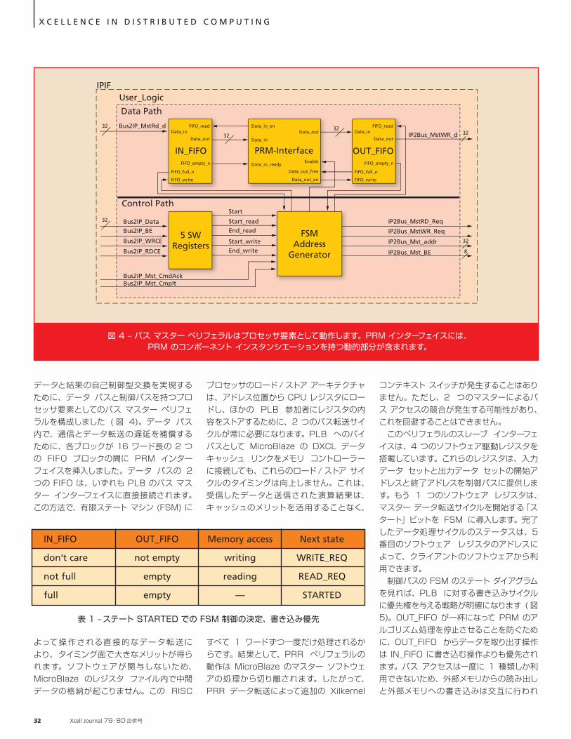
データと結果の自己制御型交換を実現するために、データ パスと制御パスを持つプロセッサ要素としてのバス マスター ペリフェラルを構成しました ( 図 4)。データ パス内で、通信とデータ転送の遅延を補償するために、各ブロックが 16 ワード長の 2 つの FIFO ブロックの間に PRM インターフェイスを挿入しました。データ パスの 2 つの FIFO は、いずれも PLB のバス マスター インターフェイスに直接接続されます。この方法で、有限ステート マシン (FSM) に
よって操作される直接的なデータ転 送により、タイミング面で大きなメリットが得られます。ソフトウェアが関与しないため、MicroBlaze のレジスタ ファイル内で中間データの格納が起こりません。この RISC
X C E L L E N C E I N D I S T R I B U T E D C O M P U T I N G
プロセッサのロード / ストア アーキテクチャは、アドレス位置から CPU レジスタにロードし、ほかの PLB 参加者にレジスタの内容をストアするために、2 つのバス転送サイクルが常に必要になります。PLB へのバイパスとして MicroBlaze の DXCL データ キャッシュ リンクをメモリ コントローラーに接続しても、これらのロード / ストア サイクルのタイミングは向上しません。これは、受信したデータと送信された演算結果は、キャッシュのメリットを活用することなく、
すべて 1 ワードずつ一度だけ処理されるからです。結果として、PRR ペリフェラルの動作は MicroBlaze のマスター ソフトウェアの処理から切り離されます。したがって、PRR データ転送によって追加の Xilkernel
コンテキスト スイッチが発生することはありません。ただし、2 つのマスターによるバス アクセスの競合が発生する可能性があり、これを回避することはできません。 このペリフェラルのスレーブ インターフェイスは、4 つのソフトウェア駆動レジスタを搭載しています。これらのレジスタは、入力データ セットと出力データ セットの開始アドレスと終了アドレスを制御パスに提供します。もう 1 つのソフトウェア レジスタは、マスター データ転送サイクルを開始する「スタート」ビットを FSM に導入します。完了したデータ処理サイクルのステータスは、5 番目のソフトウェア レジスタのアドレスによって、クライアントのソフトウェアから利用できます。 制御パスの FSM のステート ダイアグラムを見れば、PLB に対する書き込みサイクルに優先権を与える戦略が明確になります ( 図 5)。OUT_FIFO が一杯になって PRM のアルゴリズム処理を停止させることを防ぐために、OUT_FIFO からデータを取り出す操作は IN_FIFO に書き込む操作よりも優先されます。バス アクセスは一度に 1 種類しか利用できないため、外部メモリからの読み出しと外部メモリへの書き込みは交互に行われ
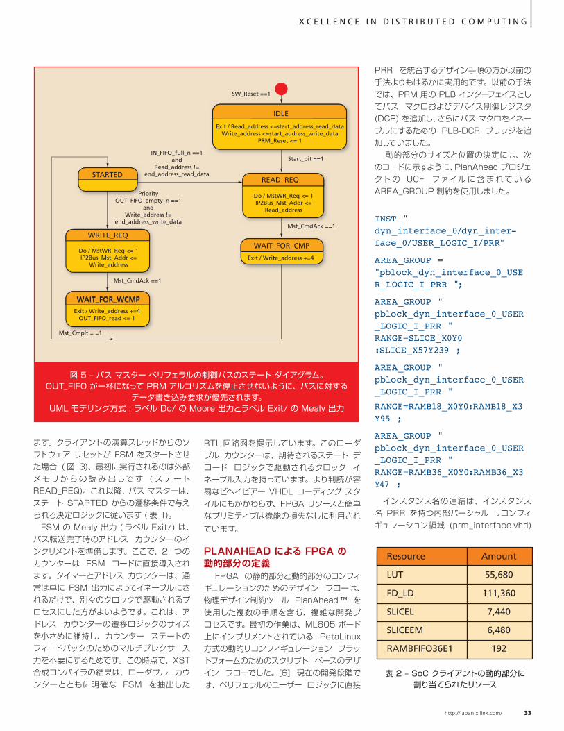
IN_FIFO OUT_FIFO Memory access Next state
don’t care not empty writing WRITE_REQ
not full empty reading READ_REQ
full empty — STARTED
表 1 – ステート STARTED での FSM 制御の決定、書き込み優先
IPIFUser_Logic
Data Path
IN_FIFO
Control Path
PRM-Interface OUT_FIFO
5 SWRegisters
FSMAddress
Generator
32Data_in
Data_in_en
Data_in
Data_in_ready
FIFO_full_n
FIFO_read
FIFO_empty_n
Data_out
Data_out
Enable
Data_out_free
Data_out_enFIFO_write
Data_in
FIFO_full_n
FIFO_read
FIFO_empty_n
Data_out
FIFO_write
3232
32
32
8
32
Bus2IP_MstRd_d
Bus2IP_Data
Bus2IP_BE
Bus2IP_WRCE
Bus2IP_RDCE
Bus2IP_Mst_CmdAck
Start
Start_read IP2Bus_MstRD_Req
IP2Bus_MstWR_Req
IP2Bus_MstWR_d
IP2Bus_Mst_addr
IP2Bus_Mst_BE
End_read
Start_write
End_write
Bus2IP_Mst_Cmplt
図 4 – バス マスター ペリフェラルはプロセッサ要素として動作します。PRM インターフェイスには、PRM のコンポーネント インスタンシエーションを持つ動的部分が含まれます。
32 Xcell Journal 79・80 合併号
ます。クライアントの演算スレッドからのソフトウェア リセットが FSM をスタートさせた場合 ( 図 3)、最初に実行されるのは外部メモリか ら の 読 み 出しで す ( ス テ ート READ_REQ)。これ以降、バス マスターは、ステート STARTED からの遷移条件で与えられる決定ロジックに従います ( 表 1)。 FSM の Mealy 出力 ( ラベル Exit/) は、バス転送完了時のアドレス カウンターのインクリメントを準備します。ここで、2 つのカウンターは FSM コードに直接導入されます。タイマーとアドレス カウンターは、通常は単に FSM 出力によってイネーブルにされるだけで、別々のクロックで駆動されるプロセスにした方がよいようです。これは、アドレス カウンターの遷移ロジックのサイズを小さめに維持し、カウンター ステートのフィードバックのためのマルチプレクサー入力を不要にするためです。この時点で、XST 合成コンパイラの結果は、ローダブル カウンターとともに明確な FSM を抽出した
X C E L L E N C E I N D I S T R I B U T E D C O M P U T I N G
RTL 回路図を提示しています。このローダブル カウンターは、期待されるステート デコード ロジックで駆動されるクロック イネーブル入力を持っています。より判読が容易なビヘイビアー VHDL コーディング スタイルにもかかわらず、FPGA リソースと簡単なプリミティブは機能の損失なしに利用されています。
PLANAHEAD による FPGA の動的部分の定義
FPGA の静的部分と動的部分のコンフィギュレーションのためのデザイン フローは、物理デザイン制約ツール PlanAhead ™ を使用した複数の手順を含む、複雑な開発プロセスです。最初の作業は、ML605 ボード上にインプリメントされている PetaLinux 方式の動的リコンフィギュレーション プラットフォームのためのスクリプト ベースのデザイン フローでした。[6] 現在の開発段階では、ペリフェラルのユーザー ロジックに直接
PRR を統合するデザイン手順の方が以前の手法よりもはるかに実用的です。以前の手法では、PRM 用の PLB インターフェイスとしてバス マクロおよびデバイス制御レジスタ (DCR) を追加し、さらにバス マクロをイネーブルにするための PLB-DCR ブリッジを追加していました。
動的部分のサイズと位置の決定には、次のコードに示すように、PlanAhead プロジェクト の UCF ファイル に 含 ま れて い る AREA_GROUP 制約を使用しました。
INST " dyn_interface_0/dyn_inter-face_0/USER_LOGIC_I/PRR"
AREA_GROUP = "pblock_dyn_interface_0_USER_LOGIC_I_PRR ";
AREA_GROUP " pblock_dyn_interface_0_USER_LOGIC_I_PRR " RANGE=SLICE_X0Y0 :SLICE_X57Y239 ;
AREA_GROUP " pblock_dyn_interface_0_USER_LOGIC_I_PRR "
RANGE=RAMB18_X0Y0:RAMB18_X3Y95 ;
AREA_GROUP " pblock_dyn_interface_0_USER_LOGIC_I_PRR " RANGE=RAMB36_X0Y0:RAMB36_X3Y47 ;
インスタンス名の連結は、インスタンス名 PRR を持つ内部パーシャル リコンフィギュレーション領域 (prm_interface.vhd)
Resource Amount
LUT 55,680
FD_LD 111,360
SLICEL 7,440
SLICEEM 6,480
RAMBFIFO36E1 192
STARTED
WRITE_REQ
WAIT_FOR_WCMPWAIT_FOR_WCMP
WAIT_FOR_CMP
READ_REQ
IDLE
IN_FIFO_full_n ==1and
Read_address !=end_address_read_data
Exit / Read_address <=start_address_read_dataWrite_address <=start_address_write_data
PRM_Reset <= 1
PriorityOUT_FIFO_empty_n ==1
andWrite_address !=
end_address_write_data
Do / MstWR_Req <= 1IP2Bus_Mst_Addr <=
Write_addressExit / Write_address +=4
Exit / Write_address +=4OUT_FIFO_read <= 1
Do / MstWR_Req <= 1IP2Bus_Mst_Addr <=
Read_address
Mst_CmdAck ==1
Mst_Cmplt = =1
Mst_CmdAck ==1
Start_bit ==1
SW_Reset ==1
図 5 – バス マスター ペリフェラルの制御パスのステート ダイアグラム。OUT_FIFO が一杯になって PRM アルゴリズムを停止させないように、バスに対する
データ書き込み要求が優先されます。UML モデリング方式 : ラベル Do/ の Moore 出力とラベル Exit/ の Mealy 出力
表 2 – SoC クライアントの動的部分に割り当てられたリソース
http://japan.xilinx.com/ 33
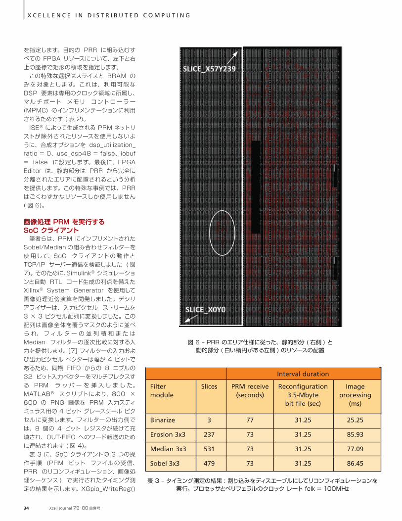
を指定します。目的の PRR に組み込むすべての FPGA リソースについて、左下と右上の座標で矩形の領域を指定します。 この特殊な選択はスライスと BRAM のみを対 象とします。これは、利 用可能 な DSP 要素は専用のクロック領域に所属し、マル チポート メモリ コント ロ ー ラ ー (MPMC) のインプリメンテーションに利用されるためです ( 表 2)。 ISE® によって生成される PRM ネットリストが除外されたリソースを使用しないように、合成オプションを dsp_utilization_ratio = 0、use_dsp48 = false、iobuf = false に設定します。最後に、FPGA Editor は、静的部分は PRR から完全に分離されたエリアに配置されるという分析を提供します。この特殊な事例では、PRR はごくわずかなリソースしか使用しません ( 図 6)。
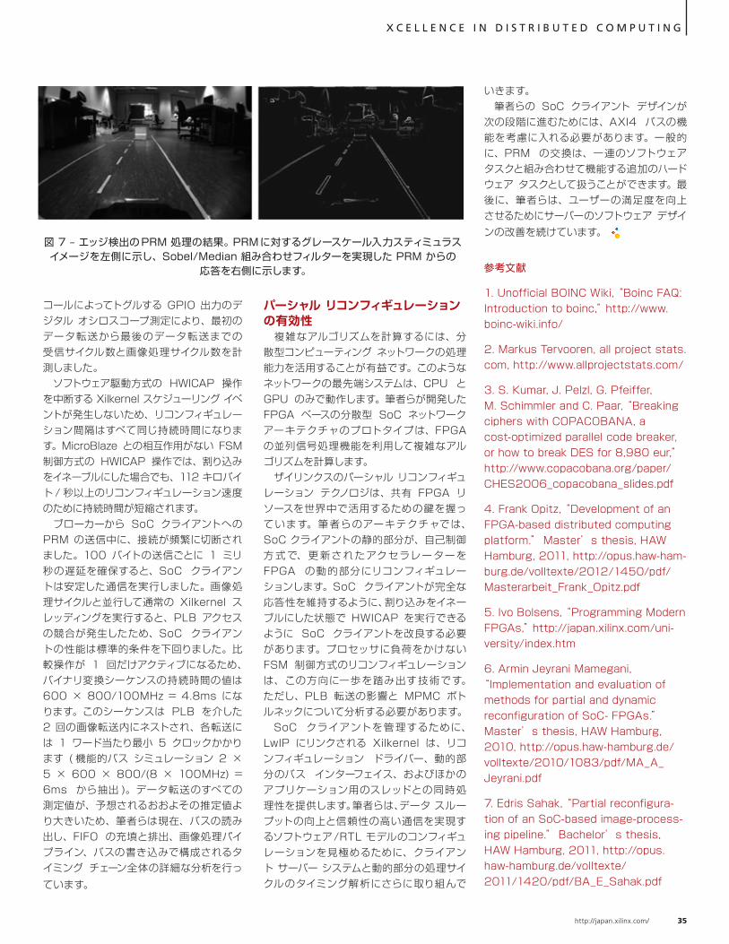
画像処理 PRM を実行するSoC クライアント 筆者らは、PRM にインプリメントされた Sobel/Median の組み合わせフィルターを使 用して、SoC クライアント の 動 作と TCP/IP サーバー通信を検証しました ( 図 7)。そのために、Simulink® シミュレーションと自動 RTL コード生成の利点を備えた Xilinx® System Generator を使用して画像処理近傍演算を開発しました。デシリアライザーは、入力ピクセル ストリームを 3 × 3 ピクセル配列に変換しました。この配列は画像全体を覆うマスクのように並べら れ、 フ ィ ル タ ー の 並 列 積 和 ま た は Median フィルターの逐次比較に対する入力を提供します。[7] フィルターの入力および出力ピクセル ベクターは幅が 4 ビットであるため、同期 FIFO からの 8 ニブルの 32 ビット入力ベクターをマルチプレクスする PRM ラ ッ パ ー を 挿 入 し ま し た。MATLAB® スクリプトにより、800 × 600 の PNG 画像を PRM 入力スティミュラス用の 4 ビット グレースケール ピクセルに変換します。フィルターの出力側では、8 個の 4 ビット レジスタが続けて充填され、OUT-FIFO へのワード転送のために連結されます ( 図 4)。 表 3 に、SoC クライアントの 3 つの操作手順 (PRM ビット ファイルの受信、PRR のリコンフィギュレーション、画像処理シーケンス ) で実行されたタイミング測定の結果を示します。XGpio_WriteReg()
X C E L L E N C E I N D I S T R I B U T E D C O M P U T I N G
Interval duration
Filter Slices PRM receive Reconfiguration Image module (seconds) 3.5-Mbyte processing bit file (sec) (ms)
Binarize 3 77 31.25 25.25
Erosion 3x3 237 73 31.25 85.93
Median 3x3 531 73 31.25 77.09
Sobel 3x3 479 73 31.25 86.45
表 3 – タイミング測定の結果 : 割り込みをディスエーブルにしてリコンフィギュレーションを実行。プロセッサとペリフェラルのクロック レート fclk = 100MHz
図 6 – PRR のエリア仕様に従った、静的部分 ( 右側 ) と動的部分 ( 白い楕円がある左側 ) のリソースの配置
34 Xcell Journal 79・80 合併号
コールによってトグルする GPIO 出力のデジタル オシロスコープ測定により、最初のデータ転送から最後のデータ転送までの受信サイクル数と画像処理サイクル数を計測しました。 ソフトウェア駆動方式の HWICAP 操作を中断する Xilkernel スケジューリング イベントが発生しないため、リコンフィギュレーション間隔はすべて同じ持続時間になります。MicroBlaze との相互作用がない FSM 制御方式の HWICAP 操作では、割り込みをイネーブルにした場合でも、112 キロバイト / 秒以上のリコンフィギュレーション速度のために持続時間が短縮されます。 ブローカーから SoC クライアントへの PRM の送信中に、接続が頻繁に切断されました。100 バイトの送信ごとに 1 ミリ秒の遅延を確保すると、SoC クライアントは安定した通信を実行しました。画像処理サイクルと並行して通常の Xilkernel スレッディングを実行すると、PLB アクセスの競合が発生したため、SoC クライアントの性能は標準的条件を下回りました。比較操作が 1 回だけアクティブになるため、バイナリ変換シーケンスの持続時間の値は 600 × 800/100MHz = 4.8ms になります。このシーケンスは PLB を介した 2 回の画像転送内にネストされ、各転送には 1 ワード当たり最小 5 クロックかかります ( 機能的バス シミュレーション 2 × 5 × 600 × 800/(8 × 100MHz) = 6ms から抽出 )。データ転送のすべての測定値が、予想されるおおよその推定値より大きいため、筆者らは現在、バスの読み出し、FIFO の充填と排出、画像処理パイプライン、バスの書き込みで構成されるタイミング チェーン全体の詳細な分析を行っています。
X C E L L E N C E I N D I S T R I B U T E D C O M P U T I N G
パーシャル リコンフィギュレーションの有効性 複雑なアルゴリズムを計算するには、分散型コンピューティング ネットワークの処理能力を活用することが有益です。このようなネットワークの最先端システムは、CPU と GPU のみで動作します。筆者らが開発した FPGA ベースの分散型 SoC ネットワーク アーキテクチャのプロトタイプは、FPGA の並列信号処理機能を利用して複雑なアルゴリズムを計算します。 ザイリンクスのパーシャル リコンフィギュレーション テクノロジは、共有 FPGA リソースを世界中で活用するための鍵を握っています。筆者らのアーキテクチャでは、SoC クライアントの静的部分が、自己制御方 式で、更新されたアクセラレーターを FPGA の動的部分にリコンフィギュレーションします。SoC クライアントが完全な応答性を維持するように、割り込みをイネーブルにした状態で HWICAP を実行できるように SoC クライアントを改良する必要があります。プロセッサに負荷をかけない FSM 制御方式のリコンフィギュレーションは、この方向に一歩を踏み出す技術です。ただし、PLB 転送の影響と MPMC ボトルネックについて分析する必要があります。 SoC クライアントを管理するために、LwIP にリンクされる Xilkernel は、リコンフィギュレーション ドライバー、動的部分のバス インターフェイス、およびほかのアプリケーション用のスレッドとの同時処理性を提供します。筆者らは、データ スループットの向上と信頼性の高い通信を実現するソフトウェア/RTL モデルのコンフィギュレーションを見極めるために、クライアント サーバー システムと動的部分の処理サイクルのタイミング解析にさらに取り組んで
いきます。 筆者らの SoC クライアント デザインが次の段階に進むためには、AXI4 バスの機能を考慮に入れる必要があります。一般的に、PRM の交換は、一連のソフトウェア タスクと組み合わせて機能する追加のハードウェア タスクとして扱うことができます。最後に、筆者らは、ユーザーの満足度を向上させるためにサーバーのソフトウェア デザインの改善を続けています。
参考文献
1. Unofficial BOINC Wiki, “Boinc FAQ: Introduction to boinc,” http://www.boinc-wiki.info/
2. Markus Tervooren, all project stats.com, http://www.allprojectstats.com/
3. S. Kumar, J. Pelzl, G. Pfeiffer, M. Schimmler and C. Paar, “Breaking ciphers with COPACOBANA, a cost-optimized parallel code breaker, or how to break DES for 8,980 eur,” http://www.copacobana.org/paper/CHES2006_copacobana_slides.pdf
4. Frank Opitz, “Development of an FPGA-based distributed computing platform.” Master’s thesis, HAW Hamburg, 2011, http://opus.haw-ham-burg.de/volltexte/2012/1450/pdf/Masterarbeit_Frank_Opitz.pdf
5. Ivo Bolsens, “Programming Modern FPGAs,” http://japan.xilinx.com/uni-versity/index.htm
6. Armin Jeyrani Mamegani, “Implementation and evaluation of methods for partial and dynamic reconfiguration of SoC- FPGAs.” Master’s thesis, HAW Hamburg, 2010, http://opus.haw-hamburg.de/ volltexte/2010/1083/pdf/MA_A_Jeyrani.pdf
7. Edris Sahak, “Partial reconfigura-tion of an SoC-based image-process-ing pipeline.” Bachelor’s thesis, HAW Hamburg, 2011, http://opus.haw-hamburg.de/volltexte/2011/1420/pdf/BA_E_Sahak.pdf
図 7 – エッジ検出の PRM 処理の結果。PRM に対するグレースケール入力スティミュラス イメージを左側に示し、Sobel/Median 組み合わせフィルターを実現した PRM からの
応答を右側に示します。
http://japan.xilinx.com/ 35
PRODUCT FEATURE
Xilinx Artix-7 FPGA Ships High-End Value to Low-Cost Market
by Mike SantariniPublisher, Xcell JournalXilinx, [email protected]
ザイリンクス、低コスト市場にハイエンドの価値を提供する Artix-7 FPGA を出荷
36 Xcell Journal 79・80 合併号
ザイリンクスはすでに、顧客の製品価値の向上をサポートする、低コスト、低消費電力の多機能 All Programmable デバイス ファミリ 2 製品の最初となる Artix ™ -7 A100T FPGA の出荷を開始し、さらに高機能な Artix-7 A200T FPGA も、まもなく出荷を予定しています。 Artix-7 デバイスの出荷は、ザイリンクスにとって画期的な出来事です。それはザイリンクスが 28nm All Programmable デバイスのすべてのファミリで FPGA の出荷を開始することを意味するからです。ザイリンクスはまた、世界初の 3D IC FPGA である Kintex™ -7 シリーズも出荷を開始しており、続いて ARM プロセッサと FPGA ロジックを同じダイ上に統合した画期的な Zynq ™ -7000 All Programmable SoC を発表しています。 ザイリンクスでプロダクト マーケティング マネージャーを務める Ehab Mohsen は、Artix-7 シリーズは顧客に広く歓迎され、これまで報道機関が「ローエンド」FPGA と呼んでいた市場に、高度な機能セット、低消費電力、コスト パフォーマンスの新たな標準を確立すると予想しています。FPGA ベンダー各社は、この市場を「価値ベース」、
「量産型」、または「コスト重視型」と呼んでいます。 「Artix-7 ファミリの機能セットを見るかぎり、この製品は「ローエンド」とはとても言えません。現在の FPGA 市場では、たしかに Artix-7 ファミリは極めてハイエンドな、最高の価値を持つ FPGA 製品ラインと言えます」と Mohsen は述べています。
「Spartan®-6 FPGA の最も高機能な製品が 15 万ロジック セルであったのに対して、Artix-7 ファミリの最初の製品は 10 万ロジック セル、最も高機能な製品では 21.5 万ロジック セルに達します」。Mohsen によると、Artix-7 FPGA の特長はロジック セル数だけにとどまらず、8 ~ 16 個の 6.6Gbpsトランシーバー、最大 13Mbit のブロック RAM、740 個もの DSP48E1 スライスを搭載しています。 ザイリンクスでストラテジック マーケティング マネージャーを務める Maureen Smerdon は、「Artix-7 フ ァ ミ リ は Spartan-6 ファミリの 2 倍のパフォーマンスを 2 分の 1 の消費電力で提供します。このデバイスは極めてハイエンドな「ローエンド」FPGA と言えます」と付け加えています。
P R O D U C T F E A T U R E
ザイリンクス、コスト重視のアプリケーションで消費電力と性能の新たな標準を確立する All Programmable Artix-7 FPGA を出荷
http://japan.xilinx.com/ 37
ドレンジ製品と同等の集積度を確保しながら、低消費電力と低コストのメリットを提供しています。DSP リソースは、競合製品の 2 倍に相当する最 大 1,306GMAC の DSP 性能を提供します。この強力な信号処理機能は、大きな処理能力を必要とする画像処理および通信アプリケーションに効果的です。 さらに、Artix-7 ファミリは、ザイリンクスが低消費電力向けに最適化した最大 16 個の 6.6Gbps コンフィギャラブル トランシーバーをサポートします。これにより、Artix-7 は、コスト重視型市場で最速の通信回線速度を提供します。これらのトランシーバーは、送信チャネル上の信号歪みを補償するプリエンファシスと連続時間リニア イコライザー (CTLE) をサポートします。
「211Gbps の 総 ス ル ープ ット に よ り、Artix-7 は、従来ミッドレンジのソリューショ
ンを必要としていた帯域幅重視のアプリケーションに低コストの代替手段を提供します」と Mohsen は述べています。 さらに、Mohsen によると、メモリ読み 出し / 書き 込 み 帯域 幅はシステム パフォーマンス 全 体 に 影 響 を与えますが、Artix-7 ファミリは、このクラスの FPGA としては業界最高となる最大 1,066Mbps の DDR3 データ レートを提供します。このメモリ ソリューションは、デザインと AMBA® AXI4 スレーブ インターフェイスを DDR3/DDR2 SDRAM デバイスへインターフェイスするための柔軟なコントローラーと物理層 (PHY) で構成されます。このコントローラーは、ビデオおよびデータ ストレージへの効率的なアクセスなど、柔
実際、Artix-7 ファミリよりも高価な競合他社の「ミッドレンジ」デバイス ファミリは、Artix-7 と同等クラスの機能セットを備えていますが、それらの製品と比べても、ザイリンクスの Artix-7 ファミリには複数のメリットがあります。
HPL と 7 シリーズの拡張性のあるアーキテクチャを活用 ザイリンクスの 28nm 世代デバイスでは、消費電力の削減が最優先課題となりました (Xcell Journal 日本語版 75・76 合併号のカバー ストーリーを参照 )。実際、ザイリンクスは TSMC 社と緊密に協力して、TSMC 社の HPL ( 高性能、低消費電力 ) 28nm シリコン製造プロセスを策定し、FPGA 生産の中心に据えました。その結果、ザイリンクスの 28nm 製品ラインのすべてで総消費電力が旧世代 FPGA の 2
分の 1 に低減できました。 「すべての製品ファミリで顧客は消費電力の削減を要求してきましたが、特にコスト重視型市場ではその要件が強調されています」と Mohsen は述べています。「これらのデバイスは、バッテリ寿命の延長、電力コストの削減、消費電力の向上、BOM コストの低減 ( 余分なシールドや電源回路が不要 )、最終製品のフォーム ファクターの小型化など、さまざまな理由で低消費電力が必要とされる各種のアプリケーションに採用されています。」 Mohsen によると、Artix-7 ファミリは、50% の消費電力削減をフルに活用して、ターゲット市場に必要な性能を提 供します。「50% の消費電力削減により、性能、
P R O D U C T F E A T U R E
ロジック密度、I/O 帯域幅、信号処理機能をさらに向上させるための余裕を確保できます」と Mohsen は述べています。これにより、設計者は「消費電力を 50% 削減するか、あるいは従来のパワー バジェットで性能と容量を拡張するかを柔軟に選択できます。」 Mohsen によると、ザイリンクスのすべての 28nm All Programmable デバイスは同じロジック アーキテクチャを採用しています。Artix-7 FPGA のスライス アーキテクチャは、Xilinx® Virtex®-6 および Spartan-6 FPGA ファミリのアーキテクチャに基づいており、同じ LUT 構造、制御ロジックおよび出力を使用しています。「この 拡 張 性 の 高 いアー キテクチャにより、Spartan-6 FPGA と Artix-7 FPGA の間でデザインの移 行は容易に行えます」と Mohsen は述べています。
ムーアの法則とロジック セルを超える進化 Artix-7 は、ザイリンクスのデバイスが従来の「FPGA」の概念を超えて急速に進化していることを示す実例と言えます。これまで長い間、FPGA の進化は、単にムーアの法則に従って 22 カ月ごとにロジック セルの数が倍増するだけであると言われてきました。しかし、ザイリンクスの最小の 28nm デバイスである Artix-7 ファミリでさえ、その予測ロジック セル数を超えるプログラマブル システム機能を搭載しています。 Mohsen によると Artix-7 は、21.5 万ロジック セル内に最大 13Mbit のブロック RAM/ ロジック比と同じ容量内に 740 個の DSP48E1 を搭載し、競合他社のミッ
AD
C
12
8 C
ha
nn
els
Deserializer
RX Beamformer Control
DataHigh-Speed I/O
ControlHigh-Speed I/O
Artix-7 FPGARX 128-Channel Beamformer
128-Channel Transducer
547 Pins (LVDS)
46 Pins
図 1 – Artix-7 FPGA の DSP 性能と I/O 数を利用した、128 チャネル携帯型超音波検査装置の例
38 Xcell Journal 79・80 合併号
P R O D U C T F E A T U R E
軟なシステム デザインを可能にする各種の外部メモリをサポートします。 このように、Artix-7 A100T デバイスは多彩なアプリケーションに理想的です。これらのアプリケーションは、顧客の技術革新、充実した新しい機能セットの顧客への提供、市場の拡大を可能にします。Mohsen は、Artix-7 FPGA ファミリの機能セットの大きな恩恵を受ける市場の例として、携帯型医療機器、ハンドヘルド無線機器、小型セルラー基地局の 3 つを挙げています。
携帯型医療機器に優れた価値を提供 Mohsen によると、医療用電子機器メーカー各社は、病院向けの非常に高価な大型検査装置以外の市場にも製品ラインを広げることを望んでいます。各社は、より低コストの携帯型電子機器を、小規模な診療所、病院の各分室、個人開業医に提供しようと務めています。 「Artix-7 FPGA の機能セットの恩恵を受ける市場の最良の例として、携帯型超音波検査装置が挙げられます」と Mohsen は述べています。「非常に大型の超音波検査システムを備えた特別室へ患者を搬送する代わりに、はるかに小さな携帯型システムをカートで ( あるいは片手で持って ) 患者のもとに運ぶことができます。救急車内の救急隊員や往診中の医師もこれらの機器を利用できます。素晴らしいことに、メーカー各社は、Artix-7 ファミリの FPGA を使用して、これまでハイエンドのシステムにしか搭載できなかった多くの先進機能を次世代の携帯型超音波検査装置に採用できます。」 ただし Mohsen によると、これらの新しいクラスの機器が従来の大型検査システムに取って代わるということではありません。
「なぜならメーカー各社は、さらに高機能な
ザイリンクスの Kintex-7 および Virtex-7 FPGA ファミリの充実した機能セットを利用して、大型検査システムにも素晴らしい新機能を追加していくからです。」 Mohsen によると、Artix-7 ファミリは、ザイリンクスの Spartan-6 デバイスに比べて静的消費電力を 65%、動的消費電力を 50% 削 減 し な が ら、 最 大 16 個 の 6.6Gbps トランシーバーを提供します。このため、携帯型超音波検査装置の設計者は、JESD204B 高速シリアル インターフェイス規格に準拠した最高の画質を達成できます。同時に、バッテリ寿命の延長と安全規格への適合を実現しながら、ほかの FPGA インプリメンテーションに比べて 41% 少ない消費電力で 128 チャネル ビームフォーマーをインプリメントできます。 図 1 に、Artix-7 が携帯型超音波検査装置 市 場 に もたらす All Programmable FPGA のメリットの例を示します。 軍用 SDR に対する BOM、重量、およびコストの削減 Mohsen によると、Artix-7 FPGA の充実した機能セットの大きな恩恵を受ける市場のもう 1 つの例として、軍用ソフトウェア無線 (SDR) が挙げられます。過去 10 年間、米軍は Global Information Grid (GIG) と呼ばれる高度な世界的通信網を着々と構築してきました (Xcell Journal 日本語版 69・70 合併号のカバー ストーリーを参照 )。この通信網により、米軍と同盟軍は世界規模の通信を行い、より正確な情報収集活動と軍事作戦を実行できます。ネットワーク機器から航空機や UAV に至るまで、高機能なザイリンクス Virtex-7 FPGA および Kintex-7 FPGA が GIG 内の大型通信機器に果たす役割は広がっています。一方で米軍は、個々の兵士を含むすべての資
産を GIG に接続するためのより良い方法を追求しています。 「現在導入されている携帯型 SDR システムの多くは、高い消費電力と短いバッテリ寿命が問題となっています」と Mohsen は述べています。「これらのシステムについては、サイズの大きさ、重量、コスト、および複雑性も問題となります。携帯型 SDR システムには、全世界の音声、データ、およびビデオ通信に対応する各種の無線プロトコルや波形をサポートする、大規模な DSP 処理機能が必要です。これらの波形をすべてサポートすることの難しさに加えて、完璧なセキュリティの確保が要求される上、無線周波数の確保が困難な苛酷な条件で動作する必要があります。したがって米軍は、バッテリ寿命の延長とセキュリティの強化を可能にする、より優れた、より軽量のシステムを常に探し求めています。」 これらのすべての要件から、Artix-7 ファミリは SDR システムに理想的と言えます。この新しいデバイスは、特に SDR モデム管理に最適です。Mohsen によると、SDR システムのモデムはベースバンド信号の前処理と RF 信号の改良を実行しますが、この処理には大量の並列処理とリコンフィギャラブル処理が必要です。「FPGA はこのアプリケーションにスムーズに適応するので、現在の大半のシステムは実際に FPGA を使用していますが、Artix-7 を使用すれば性能がはるかに向上します」と Mohsen は述べています。最大 740 個の DSP スライスを搭載する Artix-7 は、最大 1,306GMAC の DSP 性能を提供します。この性能は競合他社の FPGA の 3 倍に相当し、すべてのスタンドアロン DSP または GPU をはるかに上回っています。 101,440 のロジック セルを提供する Artix-7 は、15 × 15mm パッケージで提
Low-NoiseAmplifierSection
RFTuning
SAWFilter
A/DData
Formatting I/O
HumanInterface
Digital WidebandFront End
Software-DefinedRadio Processing
Engine
Software Control Processing Engine
EncryptionProcessing
Engine
TxRxSwitch Artix-7 FPGA
300-MHz to 2-GHzAntenna
Traditional RF Section
図 2 – ソフトウェア無線デザインのカギとなる、システム インテグレーションと Artix-7 FPGA 内の DSP 処理能力
http://japan.xilinx.com/ 39
215,360 のロジック セルを搭載しています。これにより、ワイヤレス機器メーカーは、すべての必要なパケット処理ブロック、トラフィック管理ブロック、タイミング/ 同期ブロックと 1 つの高速無線チャネルをワンチップ上に統合したバックホール ソリューションを開発できます」(Mohsen)。 また、Mohsen によると、機器ベンダー各社は、バックホール ユニットが都市部および郊外の景観を損なわないように、目立たないようにユニットをデザインする取り組みを協調して進めています。このデザイン要件を満たすには、通常はユニットの小型化が要求されますが、この場合は各ユニット
から発生する熱を効率的に放散するデザインが課題となります。Artix-7 ファミリにより、機器ベンダーは、消費電力を抑制しながらシステム全体のユニット サイズをさらに縮小できます。 図 3 に、Artix-7 FPGA が小型セル無線バックホール システムにもたらす All Programmable FPGA のメリットの例を示します。 ザイリンクスはすでに、Artix-7 A100T/A200T の出荷および AC701 評価キットの受注を開始しました。設計者の皆様は、ザイリンクスのデザイン ツールを使用して今すぐ Artix-7 ファミリのデザインを始めら れ ま す。 詳 細 は、http://japan.xilinx.com/artix7 をご覧ください。
供され、この容量レベルでは業界最小となります。ロジック容量の拡大とサイズの小型化を両立したこのデバイスを組み込めば、システムの小型化と軽量化を簡単に実現できます。 図 2 に、Artix-7 が携帯型 SDR システム 市 場 に も たらす All Programmable FPGA のメリットの例を示します。
無線バックホールの増設 Artix-7 ファミリの大きな恩恵を受けるアプリケーションのもう 1 つの例として、無線バックホールが挙げられます。Mohsen によると、今日のセルラー トラフィックの
増大は大部分が都市部および近郊地域で発生しています。この傾向に対処するため、通信事業者は、街灯柱、交通信号機、隣接する建物の壁などに小型セル基地局を導入し、ネットワーク容量の拡大を図っています。
「通信事業者は、すべての小型セルを接続してクラスターを構成し、最寄りの集約地点に接続する必要があります。そのため、最大数十マイルに及ぶマイクロ波無線リンクを提供する、低消費電力で低コストのバックホール ユニットを導入する必要があります」(Mohsen)。 従来のモバイル バックホール ユニットが通常複数のイーサネット リンクをサポートするのに対して、無線モバイル バックホールは、内部イーサネット スイッチを使用し
P R O D U C T F E A T U R E
てイーサネット リンクと無線チャネルの間でトラフィックを転送します。「バックホール ユニットの両端に高速トランシーバーが必要です。この用途には、高価な大型のデバイスに代わる理想的な低コストのデバイスとして Artix-7 FPGA が 有 効で す。Artix-7 ファミリは、16 個の 6.6Gbps トランシーバーにより、データ コンバーターに対する Jedec JESD204B 接続規格に準拠して、イーサネット リンクと RF リンクの両方に最大の帯域幅を提供します」(Mohsen)。 また、Artix-7 デバイスにより、ワイヤレス機器メーカーは、システム インテグレー
ションの向上と BOM コストの削減を達成できます。Mohsen によると、バックホール ユニットの半分は、パケット処理、トラフィック管理、タイミング同期の各ファンクションで構成されます。ユニットの残りの半分は、信号処理用のモデム チャネルをサポートします。このモデムの主な要件は、データ コンバーターとの相互接続で高いデータ スループットが得られるように、十分に高性能な DSP プロセッシング機能と高速トランシーバーを備えていることです。 「Artix-7 ファミリは、集積度、IP コアのサポート、DSP リソースの最適な組み合わせを実現しており、これらのファンクションに理想的です。Artix-7 A100T に続いて出荷を予定している Artix-7 A200T は、
Tran
scei
vers
Tran
scei
vers
AD
CD
AC
Modem
Ethernet Switch
Control Plane Processor
Traffic Management,Packet Processing
TimeSynchronization
Channel 1 RadioEthernet
Channel 2
Artix-7 FPGA
図 3 – Artix-7 FPGA を使用した、マイクロ波モバイル バックホールのためのマルチチップ機能のインテグレーション
40 Xcell Journal 79・80 合併号
XPLANATION: FPGA 101
by Adam P. Taylor Principal Engineer
EADS Astrium
DSP と数値演算関数のインプリメントに重要な CORDIC アルゴリズムの使用方法をわかりやすく解説
How to Use the CORDIC Algorithm in Your FPGA Design
FPGA デザイン内での CORDIC アルゴリズムの使用方法
42 Xcell Journal 79・80 合併号
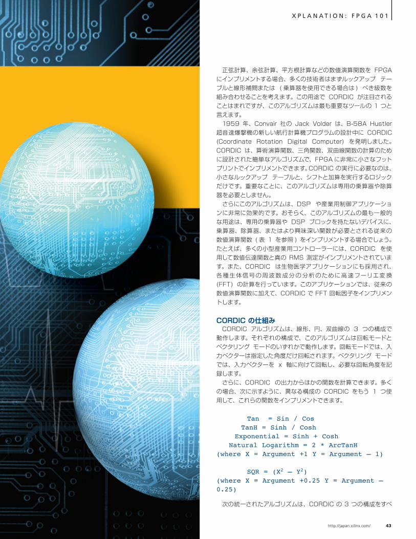
正弦計算、余弦計算、平方根計算などの数値演算関数を FPGA にインプリメントする場合、多くの技術者はまずルックアップ テーブルと線形補間または ( 乗算器を使用できる場合は ) べき級数を組み合わせることを考えます。この用途で CORDIC が注目されることはまれですが、このアルゴリズムは最も重要なツールの 1 つと言えます。 1959 年、Convair 社の Jack Volder は、B-58A Hustler 超音速爆撃機の新しい航行計算機プログラムの設計中に CORDIC (Coordinate Rotation Digital Computer) を発明しました。CORDIC は、算術演算関数、三角関数、双曲線関数の計算のために設計された簡単なアルゴリズムで、FPGA に非常に小さなフットプリントでインプリメントできます。CORDIC の実行に必要なのは、小さなルックアップ テーブルと、シフトと加算を実行するロジックだけです。重要なことに、このアルゴリズムは専用の乗算器や除算器を必要としません。 さらにこのアルゴリズムは、DSP や産業用制御アプリケーションに非常に効果的です。おそらく、このアルゴリズムの最も一般的な用途は、専用の乗算器や DSP ブロックを持たないデバイスに、乗算器、除算器、またはより興味深い関数が必要とされる従来の数値演算関数 ( 表 1 を参照 ) をインプリメントする場合でしょう。たとえば、多くの小型産業用コントローラーには、CORDIC を使用して数値伝達関数と真の RMS 測定がインプリメントされています。また、CORDIC は生物医学アプリケーションにも採用され、各種生体信号の周波数 成分の分析のために高速フーリエ変換 (FFT) の計算を行っています。このアプリケーションでは、従来の数値演算関数に加えて、CORDIC で FFT 回転因子をインプリメントします。
CORDIC の仕組み CORDIC アルゴリズムは、線形、円、双曲線の 3 つの構成で動作します。それぞれの構成で、このアルゴリズムは回転モードとベクタリング モードのいずれかで動作します。回転モードでは、入力ベクターは指定した角度だけ回転されます。ベクタリング モードでは、入力ベクターを x 軸に向けて回転し、必要な回転角度を記録します。 さらに、CORDIC の出力からほかの関数を計算できます。多くの場合、次に示すように、異なる構成の CORDIC をもう 1 つ使用して、これらの関数をインプリメントできます。
Tan = Sin / Cos TanH = Sinh / Cosh Exponential = Sinh + Cosh Natural Logarithm = 2 * ArcTanH (where X = Argument +1 Y = Argument – 1)
SQR = (X2 – Y2)(where X = Argument +0.25 Y = Argument – 0.25)
次の統一されたアルゴリズムは、CORDIC の 3 つの構成をすべ
X P L A N A T I O N : F P G A 1 0 1
How to Use the CORDIC Algorithm in Your FPGA Design
FPGA デザイン内での CORDIC アルゴリズムの使用方法
http://japan.xilinx.com/ 43
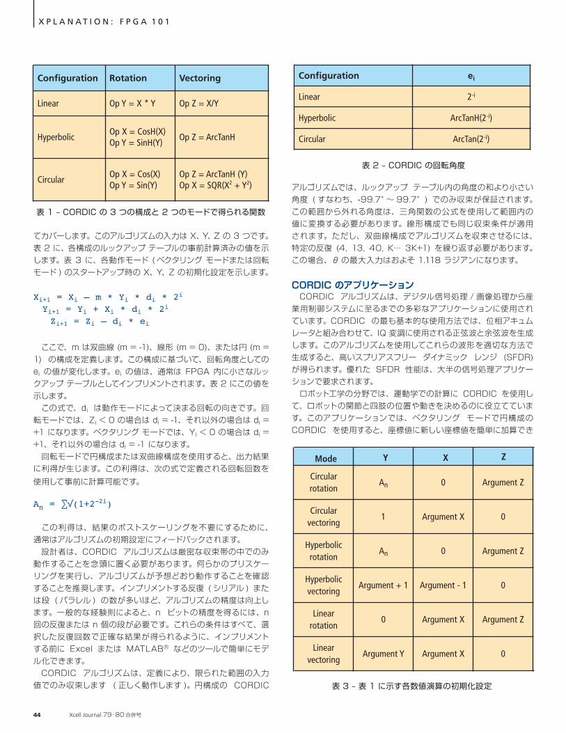
てカバーします。このアルゴリズムの入力は X、Y、Z の 3 つです。表 2 に、各構成のルックアップ テーブルの事前計算済みの値を示します。表 3 に、各動作モード ( ベクタリング モードまたは回転モード ) のスタートアップ時の X、Y、Z の初期化設定を示します。
Xi+1 = Xi – m * Yi * di * 2i Yi+1 = Yi + Xi * di * 2i Zi+1 = Zi – di * ei
ここで、m は双曲線 (m = -1)、線形 (m = 0)、または円 (m = 1) の構成を定義します。この構成に基づいて、回転角度としての ei の値が変化します。ei の値は、通常は FPGA 内に小さなルックアップ テーブルとしてインプリメントされます。表 2 にこの値を示します。 この式で、di は動作モードによって決まる回転の向きです。回転モードでは、Zi < 0 の場合は di = -1、それ以外の場合は di = +1 になります。ベクタリング モードでは、Yi < 0 の場合は di = +1、それ以外の場合は di = -1 になります。 回転モードで円構成または双曲線構成を使用すると、出力結果に利得が生じます。この利得は、次の式で定義される回転回数を使用して事前に計算可能です。
An = ∑√(1+2-2i)
この利得は、結果のポストスケーリングを不要にするために、通常はアルゴリズムの初期設定にフィードバックされます。 設計者は、CORDIC アルゴリズムは厳密な収束帯の中でのみ動作することを念頭に置く必要があります。何らかのプリスケーリングを実行し、アルゴリズムが予想どおり動作することを確認することを推奨します。インプリメントする反復 ( シリアル ) または段 ( パラレル ) の数が多いほど、アルゴリズムの精度は向上します。一般的な経験則によると、n ビットの精度を得るには、n 回の反復または n 個の段が必要です。これらの条件はすべて、選択した反復回数で正確な結果が得られるように、インプリメントする前に Excel または MATLAB® などのツールで簡単にモデル化できます。 CORDIC アルゴリズムは、定義により、限られた範囲の入力値でのみ収束します ( 正しく動作します )。円構成の CORDIC
X P L A N A T I O N : F P G A 1 0 1
アルゴリズムでは、ルックアップ テーブル内の角度の和より小さい角度 ( すなわち、-99.7°~ 99.7°) でのみ収束が保証されます。この範囲から外れる角度は、三角関数の公式を使用して範囲内の値に変換する必要があります。線形構成でも同じ収束条件が適用されます。ただし、双曲線構成でアルゴリズムを収束させるには、特定の反復 (4, 13, 40, K… 3K+1) を繰り返す必要があります。この場合、θ の最大入力はおよそ 1.118 ラジアンになります。
CORDIC のアプリケーション CORDIC アルゴリズムは、デジタル信号処理 / 画像処理から産業用制御システムに至るまでの多彩なアプリケーションに使用されています。CORDIC の最も基本的な使用方法では、位相アキュムレータと組み合わせて、IQ 変調に使用される正弦波と余弦波を生成します。このアルゴリズムを使用してこれらの波形を適切な方法で生成すると、高いスプリアスフリー ダイナミック レンジ (SFDR) が得られます。優れた SFDR 性能は、大半の信号処理アプリケーションで要求されます。 ロボット工学の分野では、運動学での計算に CORDIC を使用して、ロボットの関節と四肢の位置や動きを決めるのに役立てています。このアプリケーションでは、ベクタリング モードで円構成の CORDIC を使用すると、座標値に新しい座標値を簡単に加算でき
Configuration Rotation Vectoring
Linear Op Y = X * Y Op Z = X/Y
HyperbolicOp X = CosH(X)Op Y = SinH(Y)
Op Z = ArcTanH
CircularOp X = Cos(X)Op Y = Sin(Y)
Op Z = ArcTanH (Y)Op X = SQR(X2 + Y2)
Configuration ei
Linear 2-i
Hyperbolic ArcTanH(2-i)
Circular ArcTan(2-i)
表 1 – CORDIC の 3 つの構成と 2 つのモードで得られる関数
表 2 – CORDIC の回転角度
Mode Y X Z
Circular rotation
An 0 Argument Z
Circular vectoring
1 Argument X 0
Hyperbolic rotation
An 0 Argument Z
Hyperbolic vectoring
Argument + 1 Argument - 1 0
Linear rotation
0 Argument X Argument Z
Linear vectoring
Argument Y Argument X 0
表 3 – 表 1 に示す各数値演算の初期化設定
44 Xcell Journal 79・80 合併号
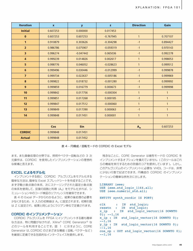
ます。また画像処理の分野では、照明やベクター回転などの 3 次元操作は、CORDIC を使用したインプリメンテーションの理想的な候補と言えます。
EXCEL によるモデル化 インプリメントする前に CORDIC アルゴリズムをモデル化する簡単な方法は、簡単な Excel スプレッドシートを作成することです。まず浮動小数点数の体系、次にスケーリングされた固定小数点数の体系を使用して、反復の回数と利得 (An) をモデル化すれば、シミュレーション中のコード検証のリファレンスを確保できます。 表 4 の Excel データからわかるように、結果の後処理の必要を少なくするため、X 入力の初期値は An に設定されます。初期引数は Z に設定され、結果と同じようにラジアン単位で定義されます。
CORDIC のインプリメンテーション CORDIC アルゴリズムを FPGA にインプリメントする最も簡単な方法は、特に問題がなければ、Xilinx® CORE Generator® などのツールを利用することです。図 1 に示すように、CORE Generator は、CORDIC のさまざまな機能 ( 回転、ベクターなど ) を厳密に定義できる包括的なインターフェイスを提供します。
X P L A N A T I O N : F P G A 1 0 1
残念なことに、CORE Generator は線形モードの CORDIC をインプリメントするオプションを備えていません ( このツールはこれらの機能を実行するための別個のコアを提供しています )。しかし、このアルゴリズムのインプリメントに必要な VHDL コードは、非常に少ない行数で記述できます。円構成の CORDIC のインプリメンテーションの簡単な例を次に示します。
LIBRARY ieee;USE ieee.std_logic_1164.all;USE ieee.numeric_std.all;
ENTITY synth_cordic IS PORT(
clk : IN std_logic;resetn : IN std_logic;z_ip : IN std_logic_vector(16 DOWNTO 0); --1,16x_ip : IN std_logic_vector(16 DOWNTO 0); --1,16y_ip : IN std_logic_vector(16 DOWNTO 0); --1,16cos_op : OUT std_logic_vector(16 DOWNTO 0); --1,16
Iteration x y z Direction Gain
Initial 0.607253 0.000000 0.017453
0 0.607253 0.607253 -0.767945 1 0.707107
1 0.910879 0.303626 -0.304298 -1 0.894427
2 0.986786 0.075907 -0.059319 -1 0.970143
3 0.996274 -0.047442 0.065036 -1 0.992278
4 0.999239 0.014826 0.002617 1 0.998053
5 0.998776 0.046052 -0.028623 1 0.999512
6 0.999496 0.030446 -0.012999 -1 0.999878
7 0.999734 0.022637 -0.005186 -1 0.999969
8 0.999822 0.018732 -0.001280 -1 0.999992
9 0.999859 0.016779 0.000673 -1 0.999998
10 0.999842 0.017756 -0.000304 1 1
11 0.999851 0.017268 0.000185 -1 1
12 0.999847 0.017512 -0.000060 1 1
13 0.999849 0.017390 0.000063 -1 1
14 0.999848 0.017451 0.000001 1 1
Cos Sin An 0.607253
CORDIC 0.999848 0.017451
Actual 0.999848 0.017452
表 4 – 円構成 / 回転モードの CORDIC の Excel モデル
http://japan.xilinx.com/ 45
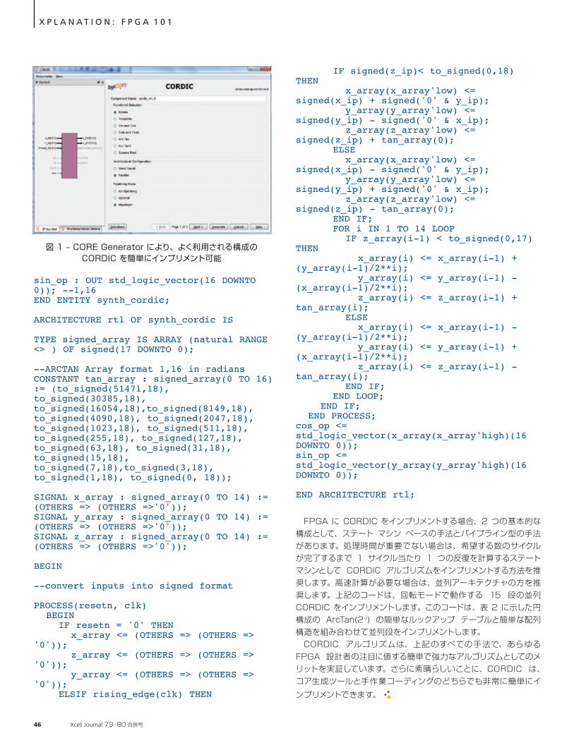
sin_op : OUT std_logic_vector(16 DOWNTO 0)); --1,16END ENTITY synth_cordic;
ARCHITECTURE rtl OF synth_cordic IS
TYPE signed_array IS ARRAY (natural RANGE <> ) OF signed(17 DOWNTO 0);
--ARCTAN Array format 1,16 in radians CONSTANT tan_array : signed_array(0 TO 16) := (to_signed(51471,18),to_signed(30385,18), to_signed(16054,18),to_signed(8149,18), to_signed(4090,18), to_signed(2047,18), to_signed(1023,18), to_signed(511,18), to_signed(255,18), to_signed(127,18), to_signed(63,18), to_signed(31,18), to_signed(15,18), to_signed(7,18),to_signed(3,18), to_signed(1,18), to_signed(0, 18));
SIGNAL x_array : signed_array(0 TO 14) := (OTHERS => (OTHERS =>'0'));SIGNAL y_array : signed_array(0 TO 14) := (OTHERS => (OTHERS =>'0'));SIGNAL z_array : signed_array(0 TO 14) := (OTHERS => (OTHERS =>'0'));
BEGIN --convert inputs into signed format
PROCESS(resetn, clk) BEGIN IF resetn = '0' THEN x_array <= (OTHERS => (OTHERS => '0')); z_array <= (OTHERS => (OTHERS => '0')); y_array <= (OTHERS => (OTHERS => '0')); ELSIF rising_edge(clk) THEN
X P L A N A T I O N : F P G A 1 0 1
IF signed(z_ip)< to_signed(0,18) THEN x_array(x_array'low) <= signed(x_ip) + signed('0' & y_ip); y_array(y_array'low) <= signed(y_ip) - signed('0' & x_ip); z_array(z_array'low) <= signed(z_ip) + tan_array(0); ELSE x_array(x_array'low) <= signed(x_ip) - signed('0' & y_ip); y_array(y_array'low) <= signed(y_ip) + signed('0' & x_ip); z_array(z_array'low) <= signed(z_ip) - tan_array(0); END IF; FOR i IN 1 TO 14 LOOP IF z_array(i-1) < to_signed(0,17) THEN x_array(i) <= x_array(i-1) + (y_array(i-1)/2**i); y_array(i) <= y_array(i-1) - (x_array(i-1)/2**i); z_array(i) <= z_array(i-1) + tan_array(i); ELSE x_array(i) <= x_array(i-1) - (y_array(i-1)/2**i); y_array(i) <= y_array(i-1) + (x_array(i-1)/2**i); z_array(i) <= z_array(i-1) - tan_array(i); END IF; END LOOP; END IF; END PROCESS; cos_op <= std_logic_vector(x_array(x_array'high)(16 DOWNTO 0));sin_op <= std_logic_vector(y_array(y_array'high)(16 DOWNTO 0));
END ARCHITECTURE rtl;
FPGA に CORDIC をインプリメントする場合、2 つの基本的な構成として、ステート マシン ベースの手法とパイプライン型の手法があります。処理時間が重要でない場合は、希望する数のサイクルが完了するまで 1 サイクル当たり 1 つの反復を計算するステート マシンとして CORDIC アルゴリズムをインプリメントする方法を推奨します。高速計算が必要な場合は、並列アーキテクチャの方を推奨します。上記のコードは、回転モードで動作する 15 段の並列 CORDIC をインプリメントします。このコードは、表 2 に示した円構成の ArcTan(2-i) の簡単なルックアップ テーブルと簡単な配列構造を組み合わせて並列段をインプリメントします。 CORDIC アルゴリズムは、上記のすべての手法で、あらゆる FPGA 設計者の注目に値する簡単で強力なアルゴリズムとしてのメリットを実証しています。さらに素晴らしいことに、CORDIC は、コア生成ツールと手作業コーディングのどちらでも非常に簡単にインプリメントできます。
図 1 – CORE Generator により、よく利用される構成の CORDIC を簡単にインプリメント可能
46 Xcell Journal 79・80 合併号
XPLANATION: FPGA 101
by Markus WedlerProf. Dr.-Ing.
Berlin Institute of Technology
Eric CrabillIP Design Engineer
Xilinx, Inc.
Graham SchelleSenior Staff Research Engineer
Xilinx, Inc.
Patrick LysaghtSenior Director
Xilinx, Inc.
ザイリンクス ソフト コアの緊密に統合されたハードウェアとファームウェアを包括的に検証する新しいフォーマル検証法
Using Formal Verification for HW/SW Co-verification of an FPGA IP Core
フォーマル検証を使用した FPGA IP コアのハードウェア/ソフトウェア協調検証
http://japan.xilinx.com/ 47
モバイル機器から車載用電子機器、産業用機械に至るまで、今日ではますます多くの製品がハードウェアとソフトウェアの機能を組み合わせて複雑な処理を行い、各種の高度なタスクを実行するようになっています。ところが、システムが複雑になるほど、ハードウェアとソフトウェアが適切に協調して動作するかを検証することは難しくなります。過去数十年にわたり、企業や研究者は、ハードウェアとソフトウェア双方の適切な機能を検証する多くの手法を考案してきましたが、この両方が意図したとおりに協調して動作することの検証は、現在も非常に難しい課題と言えます。 フォーマル検証と呼ばれる手法は、10 年以上にわたってハードウェアの適切性の検証に有望なテクノロジとして使用されてきました。たとえば、先頃インテルは、1990 年台に同社の Pentium I マイクロプロセッサの浮動小数点ユニットに重大な不具合が発生したとき、問題の修正後にフォーマル検証の手法を導入したことを明らかにしました。[1] それ以来、現在でもニッチ的な手法と考えられてはいるものの、フォーマル検証はインテルおよび業界各社のハードウェア設計チームに利用されてきました。ただしフォーマル テクニックは、ハードウェア/ ソフトウェア協調検証の手法としてはまだ広く利用されていません。 OneSpin Solutions 社、カイザースラウテルン工科大学、およびザイリンクスの研究者は、先頃、エンベデッド ファームウェアおよびハードウェア コンポーネントを含む Xilinx® ソフト IP コアの包括的検証にフォーマル テクニックを応用する方法に関する研究に着手しました。その結果、拡張性のあるフォーマル検証環境内でファームウェアとハードウェアの相互作用を捕捉できることがわかりました。業界と大学の共同研究から生まれたこのプロジェクトは、ハードウェア依存型ファームウェアのフォーマル検証に関する最新の研究成果を利用し、その研究理念はインターバル プロパティ チェック (IPC) と呼ばれる有界モデル検査の形式に基づいています。
モデル検査と IPC フォーマル検証は、数学的な手法を使用してデザインがファンクションの適切性に関する厳格な仕様に適合するかどうかを検
査するのを目的にします。まず、デザインのモデル、システムが動作する環境の記述、デザインが満たすはずの一連のプロパティを準備します。次に、あらゆるケースでプロパティが満たされるのか、それともプロパティがエラーになる条件が存在するのかを検証します。フォーマル検証と従来のシミュレーション ベースの検証法は、しだいに併用されるようになり、双方の優れた特長が利用されています。たとえば、等価チェックとアサーションは、元来はフォーマル検証から生まれた手法ですが、現在ではシミュレーション ベースの検証フローに広く組み込まれています。 モデル検査は、有限ステート マシンとして表現できるシステムに対する自動フォーマル検証の主要な手法です。システム仕様は、時相論理内の一連のプロパティとして捕捉されます。各プロパティは、時間の経過とともに一連のシステム ステートに関連する有効な ( または無効な ) 論理的挙動を指定します。たとえば、RESET プロパティは、RESET 信号がアクティブになったとき ( それまでシステムが遷移してきたステートには関係なく ) システムが RESET ステートに戻ることであるとアサートしてもよいでしょう。これらのプロパティは、SystemVerilog アサーション (SVA) などの使い慣れた言語形式で表現されます ( サイドバーの「インターバル プロパティの内容」を参照 )。
一連のプロパティは、システム仕様の抽象化モデルを形成します。モデル検査ソフトウェアが行う各プロパティの処理では、デザインのすべての到達可能なステートを漏れなく渡り歩いてプロパティの正しさを検証します。プロパティがエラーになった場合、モデル チェッカーは、プロパティを満たさなかった場所に関するリセットからのトレースを表す反例を返します。 モデル検査は自動的であり、比較的高速で実行されるメリットがあります。シミュレーション ベース検証とは異なり、モデル検査はシステム モデルを徹底的にテストするため、見つかりにくいバグが見つかることもよくあります。これらのバグは、わかりにくいまれな状況で発生する場合があります。また、検証技術者がシミュレーション テストベンチのスティミュラス テスト パターンとアサーションを作成する際に、バグが発生する条件を見逃している可能性もあります。 多数のステート変数を含む現在のシステムには、到達可能なステートの数が急激に増加する、いわゆる「ステート空間の爆発的増加」の問題が頻繁に発生します。こうしたシステムでは、ステート空間の複雑性が従来のモデル チェッカーの能力を簡単に超えてしまうため、この手法の現実的な有効性は限られたものになります。この制約が新たな形式のモデル検査の開発を促しました。こうした手法の 1 つが、筆者らが
X P L A N A T I O N : F P G A 1 0 1
インターバル プロパティの内容
PropertyADD_INSTRUCTION; t##0 ready_to_issue_instr() and t##0 decode(ADD,op1,op2,res)implies t##1 pc_updated() and t##2 reg(res)=reg(op1)+reg(op2)endproperty
次の例は、プロセッサ内の ADD 命令のオペレーションを記述する、簡単な SVA 形式のプロパティの擬似コードを示しています。ご覧のように、時間 0 で ADD 命令と 2 つのオペランドがフェッチされ、2 サイクル後にレジスタは 2 つのオペランドの和で適切に更新されます。
48 Xcell Journal 79・80 合併号
ことになります。 エンベデッド ファームウェアとハードウェアとの相互作用を検証するタスクの増大に対してフォーマル検証法を適用する課題については、活発な研究が現在進行形で進められています。これまではファームウェアとハードウェアのコンポーネントを別々に検証することが一般的でしたが、このプロセスでは最後にシステム全体のインテグレーションに時間がかかっていました。これまでインターバル プロパティ チェックは、主にハードウェア サブシステムのフォーマル検証に適用されていました。しかし、先頃発表された研究により、この手法をハードウェアとファームウェアで構成されるより完全なシステムへ拡張する方法が示されました。筆者らの研究の焦点は、ザイリンクスの市販ソフト IP コアに IPC を適用し、ファームウェアとハードウェアおよび両者の相互作用を記述する統一されたフォーマル検証環境を評価することです。このコアはソフト エラー軽減 (SEM) コア (http://japan.xilinx.com/products/intellectual-property/SEM.htm) と呼ばれ、レジスタ トランスファー レベル (RTL) ロジックと PicoBlaze ™ マイクロコントローラーを搭載しています。
SEM コア 検証タスクをよく理解できるように、まずソフト IP コアをもっと詳しく検討しましょう。このザイリンクス ソフト IP コアは、ザイリンクス FPGA のコンフィギュレーション メモリ内でのエラーの検出、分類、修正が可能です。また、テスト目的でのエラーの注入も行えます。 最新の半導体デバイスは、高レベル放射線による外乱に敏感です。たとえば、高エネルギー中性子は、シングル イベント アップセット (SEU) を発生させてコンフィギュレーション メモリ セルの状態を変化させ、チップに影響を与えることがあります。このような効果を軽減するために、ザイリンクス FPGA のコンフィギュレーション フレームのメモリ セルは、シングル エラー コレクション / ダブル エラー ディテクション ハードウェア ブロックで保護されています。宇宙船内での計測などの特定のアプリケーションでは、極めて高レベルの放射線の影響を打ち消すために、さらに高度な方法が必要になります。SEM コアは、ザイリンク
このプロジェクトで使用したインターバル プロパティ チェック (IPC) です。[2] IPC は、有界モデル チェッカーとして知られる手法の特殊な例です。ほかの有界モデル チェッカーと同じように、IPC は、プロパティの範囲を有限数のクロック サイクルに制限することで全体的な複雑性を抑制し、ブール充足可能性 (SAT) ソルバーを使用して実際のモデル検査を実行します。IPC が従来の有界モデル チェッカーと異なる点は、クロック サイクルにウィンドウを設け、そのウィンドウ内の任意の時刻からプロパティがスタートするようにアサートできることです。 また IPC では、直感的な手法でステート空間の爆発の問題に対処できます。IPC メソッドは、デザインの抽象化を利用して、ユー ザ ー に よ る 概 念 ス テ ート マ シ ン (CSM) の作成をサポートします。CSM は、検証対象のデザインの主要な機能を表現しており、特定のデザイン内のすべての重要なオペレーションまたはトランザクションを捕捉します。最上位の抽象化レベルでは、CSM 内のステート間の各遷移は、固有のプロパティによってカバーされる一体 不 可分な 動 作を 表します。実 際には、CSM は元になるデザインを抽象化したビューであるため、各 CSM トランザクションは、対応する RTL コード内の数百クロック サイクルにわたる関連信号の動作に対応することがあります。適切に定義されたプロパティは、プロパティが抽象化するインターバル全体について、すべての最も関連性の高いステートと入力 / 出力信号の挙動をサイクル精度レベルで捕捉します。各プロパティは、CSM の 1 つの遷移またはオペレーションに厳密に対応する、マルチサイクル インターバル内の予想される挙動を指定します。したがって、この手法はインターバル プロパティ チェックまたは ( 同じ意味で ) オペレーション方式のインターバル プロパティ チェックと呼ばれます。 CSM の抽象化は、基礎となる RTL デザインの詳細のすべては捕捉しないようにしています。この手法は、システムの挙動全体の捕捉に重要な一部の制御ステートだけを分析し、ステート空間とステート遷移の複雑性を削減します。この点で、IPC は標準的なアサーション ベース検証とは異な
X P L A N A T I O N : F P G A 1 0 1
ります。アサーション ベース検証では、設計者がローカル信号レベルのアサーションを RTL コードに追加し、シミュレーションまたは可能であればフォーマル テクニックを使用してそれらのアサーションをチェックします。通常このようなアサーションは、設計者が RTL コードの対応する部分をインプリメントする際に推 測した前 提 条 件をチェックすることになります。ただし、これらのローカル アサーションが IP ブロックの仕様にどのように関連付けられるかは不明確です。さらに、これらの手作業で生成されたアサーションはコード ベース全体に分散しているため、アサーションがデザインの機能全体をどの程度カバーしているかを判断するのは簡単ではありません。 次に、起こり得るすべてのステート遷移が自動的かつ徹底的に分析され、それらに対応するプロパティが検証されます。すべてのエラーは、エラーをトリガーした反例の詳細と一緒にハイライトされます。OneSpin 360 MV フォーマル検証ツールを使用したオペレーション方式の IPC では、自動的な完全性実証分析も実行できます。これは CSM プロパティの検証に使用されるのと同じ最先端のプロパティ チェック テクノロジによって実現される機能であり、このテクノロジはブール充足可能性問題の効率的なソルバーに基づいています。 完全性実証は、すべての可能な入力シーケンスに対して、オペレーション プロパティの 1 つの固有のチェーンによってデザインの 挙 動が決まることを保 証します。このチェーン内の複数のプロパティは、CSM 内の抽象化開始ステートおよび終了ステートによって連結されます。入力トリガーは分析対象のそれぞれの入力トレースと一致します。しかも、この分析は、各プロパティが特定のタイム インターバルの範囲内のすべての関連する出力信号を個々に指定していることと、出力の挙動を記述する際にこれらのインターバルが隙間なく連結されていることをチェックします。 この方法で、完全性実証は一連のプロパティの全体に対するチェックとなります。このチェックに合格した場合、この一連のプロパティによってデザインの挙動が決定されないまま残るような入力シナリオは存在しません。したがって、このプロパティ セットはデザインの機能を完全に捕捉している
http://japan.xilinx.com/ 49
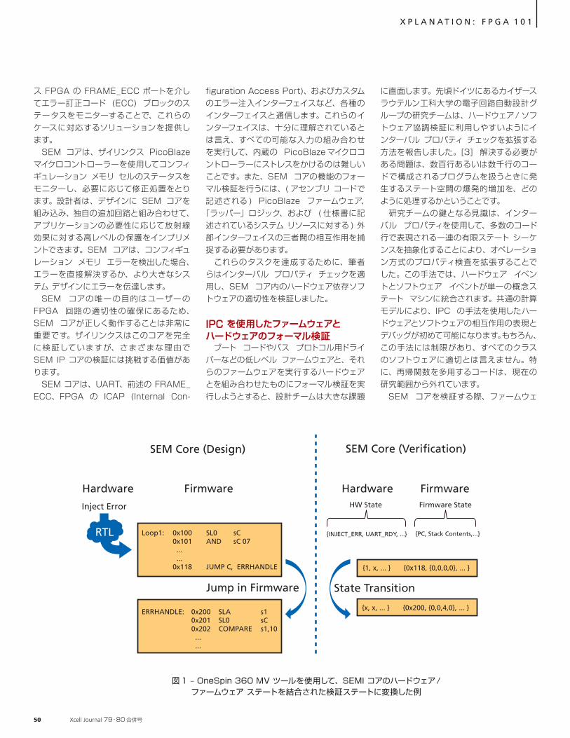
X P L A N A T I O N : F P G A 1 0 1
ス FPGA の FRAME_ECC ポートを介してエラー訂正コード (ECC) ブロックのステータスをモニターすることで、これらのケースに対応するソリューションを提供します。 SEM コアは、ザイリンクス PicoBlaze マイクロコントローラーを使用してコンフィギュレーション メモリ セルのステータスをモニターし、必要に応じて修正処置をとります。設計者は、デザインに SEM コアを組み込み、独自の追加回路と組み合わせて、アプリケーションの必要性に応じて放射線効果に対する高レベルの保護をインプリメントできます。SEM コアは、コンフィギュレーション メモリ エラーを検出した場合、エラーを直接解決するか、より大きなシステム デザインにエラーを伝達します。 SEM コアの唯一の目的はユーザーの FPGA 回路の適切性の確保にあるため、SEM コアが正しく動作することは非常に重要です。ザイリンクスはこのコアを完全に検証していますが、さまざまな理由で SEM IP コアの検証には挑戦する価値があります。 SEM コアは、UART、前述の FRAME_ECC、FPGA の ICAP (Internal Con-
figuration Access Port)、およびカスタムのエラー注入インターフェイスなど、各種のインターフェイスと通信します。これらのインターフェイスは、十分に理解されているとは言え、すべての可能な入力の組み合わせを実行して、内蔵の PicoBlaze マイクロコントローラーにストレスをかけるのは難しいことです。また、SEM コアの機能のフォーマル検証を行うには、( アセンブリ コードで記述される ) PicoBlaze ファームウェア、
「ラッパー」ロジック、および ( 仕様書に記述されているシステム リソースに対する ) 外部インターフェイスの三者間の相互作用を捕捉する必要があります。 これらのタスクを達成するために、筆者らはインターバル プロパティ チェックを適用し、SEM コア内のハードウェア依存ソフトウェアの適切性を検証しました。
IPC を使用したファームウェアとハードウェアのフォーマル検証 ブート コードやバス プロトコル用ドライバーなどの低レベル ファームウェアと、それらのファームウェアを実行するハードウェアとを組み合わせたものにフォーマル検証を実行しようとすると、設計チームは大きな課題
に直面します。先頃ドイツにあるカイザースラウテルン工科大学の電子回路自動設計グループの研究チームは、ハードウェア/ ソフトウェア協調検証に利用しやすいようにインターバル プロパティ チェックを拡張する方法を報告しました。[3] 解決する必要がある問題は、数百行あるいは数千行のコードで構成されるプログラムを扱うときに発生するステート空間の爆発的増加を、どのように処理するかということです。 研究チームの鍵となる見識は、インターバル プロパティを使用して、多数のコード行で表現される一連の有限ステート シーケンスを抽象化することにより、オペレーション方式のプロパティ検査を拡張することでした。この手法では、ハードウェア イベントとソフトウェア イベントが単一の概念ステート マシンに統合されます。共通の計算モデルにより、IPC の手法を使用したハードウェアとソフトウェアの相互作用の表現とデバッグが初めて可能になります。もちろん、この手法には制限があり、すべてのクラスのソフトウェアに適切とは言えません。特に、再帰関数を多用するコードは、現在の研究範囲から外れています。 SEM コアを検証する際、ファームウェ
RTL
Hardware Firmware
Jump in Firmware State Transition
SEM Core (Design) SEM Core (Verification)
Inject Error
Hardware Firmware
Loop1: 0x100 SL0 sC 0x101 AND sC 07 ... ... 0x118 JUMP C, ERRHANDLE
ERRHANDLE: 0x200 SLA s1 0x201 SL0 sC 0x202 COMPARE s1,10 ... ...
{1, x, ... } {0x118, {0,0,0,0}, ... }
{x, x, ... } {0x200, {0,0,4,0}, ... }
HW State Firmware State
{INJECT_ERR, UART_RDY, ...} {PC, Stack Contents,...}
図 1 – OneSpin 360 MV ツールを使用して、SEMI コアのハードウェア/ファームウェア ステートを結合された検証ステートに変換した例
50 Xcell Journal 79・80 合併号
ア制御フロー グラフ (CFG) を使用してプロパティ テンプレートを生成しました。基本ブロック間の各遷移は、PicoBlaze マイクロコントローラー内部のレジスタまたは外部のイベントによってトリガーされる別々のプロパティとして扱われます。特定のサイクルにおける、抽象化開始ステートおよび終了ステートを記述するファンクションは、単に PicoBlaze アーキテクチャ ステートと外部のスティミュラスによって決まります。 IPC によって要求されるアサーションの始まりと終わりの SEM コア ステートを記述する際に、PicoBlaze ファームウェアと FPGA ロジックの RTL コードの両方を検討する必要がありました。図 1 にファームウェア ステートとハードウェア ステートの組み合わせを示します。PicoBlaze マイクロコントローラーは真にソフトウェア有限ステート マシンをインプリメントしており、その挙動はラッパー ハードウェアに直接関連付けられていることに注意してください。PicoBlaze ファームウェアだけを切り離して検証することも可能ですが、そのためにはハードウェア バス ファンクション モデル (BFM) インターフェイスが必要になり、基本的にビヘイビアー テストベンチをもう 1 つ作成することになります。一方、IPC を拡張すれば、単一の検証環境内でハードウェアとファームウェアを含むシステム全体の挙動をモデル化することが可能です。命令セット シミュレータ内でファームウェアの実行とコンパイルを行うこともできたのですが、この方法では 1 つの環境でハードウェアおよびファームウェアで構成されるシステムの挙動を完全に捕捉することはできなかったでしょう。それに対して、IPC を利用すれば、単一のハードウェア/ ファームウェア検証環境が得られます。 プロパティを構築する際、プロパティの複雑性を反復的に制限すれば、特定のプロパティの複雑性と OneSpin 360 MV ツール内でのプロパティの評価時間の間に受け入れ可能なトレードオフを設定できます。このプロジェクトでは、プロパティのインターバルを 100 サイクル以下に維持すると、プロパティを 30 分以内に検証できることがわかりました。 さらに、SEM コア内には、プロパティの複雑性の軽減に貢献するデザイン要因
X P L A N A T I O N : F P G A 1 0 1
が存在します。SEM コア ファームウェアと PicoBlaze マイクロアーキテクチャの特性 ( そして、それらのインプリメンテーションがどのようにプロパティの作成を簡略化するか ) が、ここでの検討の対象になります。 第 1 に、SEM コアのエンベデッド ファームウェアの次のような特性を利用できます。
■ このファームウェア イメージは、ソフトウェア有限ステート マシンをインプリメントします。このステート マシンは、プロセッサ ステートのフォーマル記述に有利ないくつかの特性を持っています。特に、このファームウェアは、メモリの動的な割り当てや無制限な再帰関数の呼び出しを行いません。このことは低レベルのエンベデッド ソフトウェアでは一般的です。このファームウェアの 2 つの特性により、プロセッサ ステートとそのメモリのモデル化は大幅に簡略化されます。
■ グローバル変数とローカル変数の明示的なメモリ マップが検証に利用できます。ファームウェア内のステート遷移のトリガーに使用される、ラッパー RTL 内のすべての外部変数は、SEM コア内で利用できるので、OneSpin 360 MV ツールによる分析用に使用できます。
■ 最後に、ファームウェアのマシン コードは SEM コア内の ROM に格納されています。この ROM は検証プロセスから見えるため、PicoBlaze マイクロコントローラー上で実行される可能性があるプログラムをすべて完全に検証する必要はなく、ROM に格納される実際のプログラムだけを検証すれば十分です。つまり、実績ある PicoBlaze マイクロコントローラーがすべてのファームウェアに有効であることを再検証する必要はありません。その代わり、PicoBlaze マイクロコントローラーと SEM コアのファームウェアおよびラッパー RTL の間の相互作用だけに焦点を合わせて分析ができます。
第 2 に、PicoBlaze マイクロアーキテクチャの特性を利用して、ファームウェア イメージのステートを記述できます。PicoBlaze マイクロアーキテクチャは、フォーマル検証ツール フローへのインテグレーションを簡略化する次のような特性を持っています。
■ 命令はインオーダー実行されます。SEMコア内で割り込 みが 発 生しないため、ファームウェア内のほかの命令との関連で命令がどの時点で開始されるかが正確にわかります。
■ すべての命令は 2 サイクルでデコード /実行されます。SEM コア ファームウェア内のオペレーションのレイテンシはこのように一定であり、複数の命令を実行する際の全体的なレイテンシが決まっているため、複数の命令をカプセル化するプロパティの作成が可能です。
■ PicoBlaze マイクロアーキテクチャのスタックの深さは有限です。このスタックの内容が SEM コア ステートの主要な部分ですが、スタックの深さが有限であるため、ステート数の増加は設定された深さの範囲内に抑えられます。ステートの数が増えるほどプロパティ検証の複雑性が増すため、スタックの深さを設定することで検証を簡略化できます。
特定のサイクルでのプロセッサ ステートを記述する際に、このように少量のアーキテクチャ ステートを記述するのは比較的簡単です。この管理しやすいステート記述は、OneSpin 360 MV のプロパティ生成ツールに直接フィードされます。 これらの簡略化の要因を準備した上で、関連するステート遷移を記述する必要があります。ファームウェアの基本ブロックを個々のデザイン ステートとしてマップすれば、ステートの遷移を直接的に記述できます。定義上、基本ブロックは命令の線形シーケンスで構成されます。それぞれの条件付きジャンプまたは条件付き関数呼び出しによって、基本ブロックの終点と 2 つの可能な後継ブロックが決定されます。これらの命令のデスティネーション アドレスは、新しい基本ブロックの始点を提示します。制御フロー グラフは、基本ブロックとそれらの後継ブロックの関係で構成されます。グラフ内の各エッジはファームウェアの条件付き分岐に対応し、分岐条件のラベルが付けられます。 ファームウェアが高級言語を使用してインプリメントされている場合は、コンパイラは CFG を自動的に生成できます。ただし、( シンボリック ) 命令セット シミュレータの
http://japan.xilinx.com/ 51
助けを借りて、同じようにアセンブリ コードから CFG を抽出することもできます。この手法により、アセンブリ コードだけが利用できるレガシー プラットフォームの協調検証も可能になります。 筆者らは、SEM コアを検証する際に、ファームウェアの CFG を使用してプロパティ テンプレートを生成しました。基本ブロック間の各遷移は、PicoBlaze マイクロコントローラー内部のレジスタまたは外部イベントによってトリガーされる別々のプロパティとして扱われます。特定のサイクルでの抽象化開始ステートおよび終了ステートを 記 述 す る フ ァン ク シ ョ ン は、 単 に PicoBlaze アーキテクチャ ステートと外部のスティミュラスによって決まります。 外部のスティミュラスをアーキテクチャ ステートへマップする際の一環として、すべての条件付きジャンプまたは関数呼び出しの分岐条件を指定する必要があることがわかりました。筆者らの関心はデザインの全体的な挙動にあったため、エンベデッド プロセッサのローカル ステータス レジスタではなく、外部入力イベントまたはラッパー回路の重要なステート レジスタとの関連でこの条件を指定しました。トリガー条件で評価されるラッパーのレジスタは、抽象化
X P L A N A T I O N : F P G A 1 0 1
ステート定義の一部になります。 SEM コア ファームウェアと PicoBlaze マイクロコントローラーそれ自体が検証を簡略化する条件を備えているため、プロセッサ ステートと外部のスティミュラスとの関連ですべてのステート遷移を定義できま し た。 こ の ス テ ート に は、OneSpin 360 MV ツール内でデザインの全体的な挙動を抽象化概念有限ステート マシンに関連付けるファームウェアとハードウェアが含まれています。
プロパティの生成 SEM コアのファームウェアとハードウェアは、デザインとそのインターフェイスのエンドツーエンドの機能を捕捉する 1,700 個のプロパティで記述できることがわかりました。筆者らは、OneSpin 360 MV を使用してプロパティをチェックし、プロパティ セット全体の完全性を検証しました。プロパティは並列処理で検証可能でしょうが、サーバー クラスター内での最長のプロパティの検証時間はおよそ 30 分でした。 一見すると、合計 1,700 個のプロパティは数が多すぎるようにも思われますが、これらのプロパティの大半 ( およそ 1,500 個 ) は、主にデバッグ目的で、コントローラーからのステート情報のダンプに使用されるシーケンシャル UART 用の wait ループのみを扱っています。各プロパティは条件付きジャンプで終わる基本ソフトウェア ブロックです。したがって、このフォーマル モデルでは UART の各 wait ループは固有のプロパティを作成します。筆者らは、デザインを完全に検証するために、これらの wait ループの間に予想外の副次的作用によって抽象化ステートの内容が壊れていないことを確認しました。 生 成されたプロパティは、総体としてファームウェアの制御フロー全体をカバーします。各プロパティは、それに対応するファームウェア基本ブロックの実行時のデザインの入力 / 出力動作を記述します。この事例では、これらのプロパティが既存の検証テストベンチを補完することで、コアの機能について極めて高い確信が得られました。 生成されたプロパティによって、SEM コアのエラー注入テスト機能が、コンフィギュレーション メモリの意図しない位置にエ
ラーを注入してしまうシナリオが明らかになりました。この状況は、SEM コア製品ドキュメントの推奨事項に反する方法でエラー注入ポートを使用した場合にのみ発生します。このシナリオは通常の動作条件では起こり得ないものですが、ザイリンクスは SEM コアをアップデートし、その可能性を完全に解消しました。
高品質への取り組み 筆者らの研究は、ザイリンクス SEM コアの緊密に統合されたハードウェアとファームウェアのフォーマル検証にインターバル プロパティ チェックを利用できることを実証しました。SEM コアは、並列処理で検証される 1,700 個のプロパティを使用して、単一の検証環境内で包括的に検証されました。このプロジェクトでは、最先端の手法とツールを利用してフォーマル検証を実行しました。その結果、SEM コアの機能の適切さについて高い確信が得られました。この結果は、高品質の IP ディストリビューションに向けたザイリンクスの継続的な取り組みの成果を示しています。
参考文献
1. Jones, R.B.; O’Leary, J.W.; Seger, C.-J.H.; Aagaard, M.D.; Melham, T.F.;
“Practical formal verification in microprocessor design,” Design & Test of Computers, IEEE, vol. 18, no. 4, pp. 16-25, July/August 2001
2. Nguyen, M.D.; Thalmaier, M.; Wedler, M.; Bormann, J.; Stoffel, D.; Kunz, W.; “Unbounded protocol com-pliance verification using interval property checking with invariants,” IEEE Transactions on Computer-Aided Design of Integrated Circuits and Systems, vol. 27, no. 11, pp. 2068-2082, November 2008
3. Nguyen, M.D.; Wedler, M.; Stoffel, D., and Kunz, W.; “Formal hardware/software co-verification by interval property checking with abstraction,” Design Automation Conference (DAC), 48th ACM/EDAC/IEEE, pp. 510-515, June 5-9, 2011
欧州における IPC の起源
オペレーション方式のインターバル プ ロ パ ティ チ ェッ ク は、 欧 州 の Infineon Technologies 社の産業研究を起源としています。その中核的なテクノロジは、OneSpin Solutions 社によって採用、商用化され、開発と改良が続けられています。また同社は、専門家以外のユーザーも IPC の手 法 を 簡 単 に 利 用 で きる ように、360 MV と呼ばれる包括的な CAD 環境を提供しています。IPC の登場以来、ドイツにあるカイザースラウテルン工科大学の研究者は、Infineon Technologies 社および OneSpin Solutions 社と協力して、IPC の基礎理論のさらなる発展と IPC の応用範囲の拡大に取り組んでいます。
52 Xcell Journal 79・80 合併号
XPLANATION: FPGA 101
The FPGA Engineer’s Guide to Using ADCs and DACs
by Adam TaylorPrincipal Engineer
EADS Astrium
FPGA エンジニア ガイド : ADC と DAC の使用法
http://japan.xilinx.com/ 53
FPGA ベースのシステムは、目的のタスクを実行した後、実世界とのインターフェイスをとる必要があります。技術者なら誰でも知っているように、多くの実世界はデジタル信号ではなくアナログ信号で機能しています。つまり、デジタル ドメインとアナログ ドメイン間の変換が必要なのです。多くの選択肢の中からジョブに合った FPGA を選ぶのと同じように、ADC や DAC も多くの選択肢の中からシステムに合ったものを選ぶ必要があります。 まず最初に、信号の変換に必要なサンプリング レートを決める必要があります。このパラメーターは、コンバーターの選択だけでなく、FPGA の選択にも影響を与えます。デバイスは必要な処理速度とロジック フットプリントに対応できなければなりません。コンバーターのサンプリング レートは、サンプリングされる信号の少なくとも 2 倍は必要です。したがって、50MHz の信号をサンプリングする必要がある場合は、コンバー ター の サンプリング レートは 100MHz 以上でなければなりません。コンバーターのサンプリング レートがこれより低いと、変換された信号が自分自身にエイリアシングされ、正しく表現されません。ただし、エイリアシングは常に有害であるとは限りません。実際、コンバーターの帯域幅が十分に広ければ、エイリアシングを利用して信号を折り返し、使用に適した帯域幅に収めることができます。
ADC と DAC の主要なパラメーター アナログ デジタル コンバーターは、さまざまな手法で作成されます。一般的な手法として、フラッシュ方式、ランプ方式、および逐次比較方式が挙げられます。
処 理 速 度の 速さを 特 徴とするフラッシュ コンバーターは、一連のスケーリングされたアナログ コンパレータを使用して、参照電圧に対して入力電圧を比
較します。ADC はこれらのコンパレータの出力を用いてデジタル コードを決定します。
ランプ コンバーターは、デジタル アナログ コンバーターに接続されたフリーランニング カウンターを利用して、入力電圧に対して DAC の出力を比較します。両者が等しいときのカウントが結果として保持されます。
逐次比較 (SAR) コンバーターは、ランプ コンバーターの応用版であり、アナログ入力に対して DAC とコンパレータを利用します。ただし、SAR コンバーターは、カウントアップする代わりに、カウントのアナログ表現が入力信号より上か下かを判断し、試行錯誤に基づくデジタル コードの決定を可能にします。
デジタル アナログ コンバーターも各種の手法でインプリメントされます。最も一般的な手法として、2 進重み付け方式、R-2R ラダー方式、およびパルス幅変調方式が挙げられます。
2 進重み付け方式は、非常に高速な DAC アーキテクチャの一つです。2 進重み付けコンバーターは、各ロジック ビットの個々の変換結果の和を求めます。たとえば、抵抗ベースの DAC は、現在のコードに基づいて抵抗のオンとオフを切り替えます。
R-2R ラダー コンバー ターは、値 R-2R のカスケード接続された抵抗の構造を使用します。高精度の抵抗の作成とマッチングが容易なため、R-2R ラダー方式の DAC は 2 進重み付け方式の DAC より高精度です。
パ ルス 幅 変 調 方 式 は、 最 も 簡 単 な DAC アーキテクチャです。このアーキテクチャは、PWM 波形を簡単なロー
パス アナログ フィルターに通します。パルス幅変調コンバーターは、一般にモーター制御に使用されていますが、デルタシグマ コンバーターの基礎にもなっています。
多くの専門デバイス メーカーは、社内独自の変換アーキテクチャを開発し、使用目的に応じた特定の分野で、可能な最高のパフォーマンスを提供しています。これらの多彩な ADC/DAC デバイスには、変換速度、精度、分解能に関する長所と短所があります。FPGA を選択するときのように、I/O の数、サポートしている I/O 規格、クロック管理、ロジック リソース、およびメモリを検討する必要があります。また同時に、コンバーター デバイスに固有のパラメーターである、最大サンプリング レート、信号対ノイズ比 (SNR)、スプリアス フリー ダイナミック レンジ (SFDR)、および有効ビット数 (ENOB) を検討する必要があります。 サンプリング周波数は非常に簡単です。この値は、ADC が入力をデジタル化できる最大レートです。信号対ノイズ比は、ノイズ レベルに対する信号の比を表します。この値は入力信号と相関しないことが前提とされています。信号対ノイズ比は、理論的には次の式を使用して計算できます。
SNR = 6.02N + 1.76 dB
ここで、N は分解能(有効ビット数)です。この式はフルスケール正弦波に対して有効です。 出力の高速フーリエ変換 (FFT) を計算し、入力信号の値とノイズ フロア間の比を測定することにより、システム テスト中に実際の SNR(信号対ノイズ比)を求めることができます。 一方、SFDR は、入力信号と次の最高ピーク ( 通常は基本信号の高調波 ) 間の比です。通常、SFDR は dBc で表現され、入力信号電力の低下とともに劣化します。
X P L A N A T I O N : F P G A 1 0 1
信号処理 FPGA と実世界とのインターフェイスに必要なアナログ デジタル コンバーターとデジタル アナログ コンバーターの使い方
54 Xcell Journal 79・80 合併号
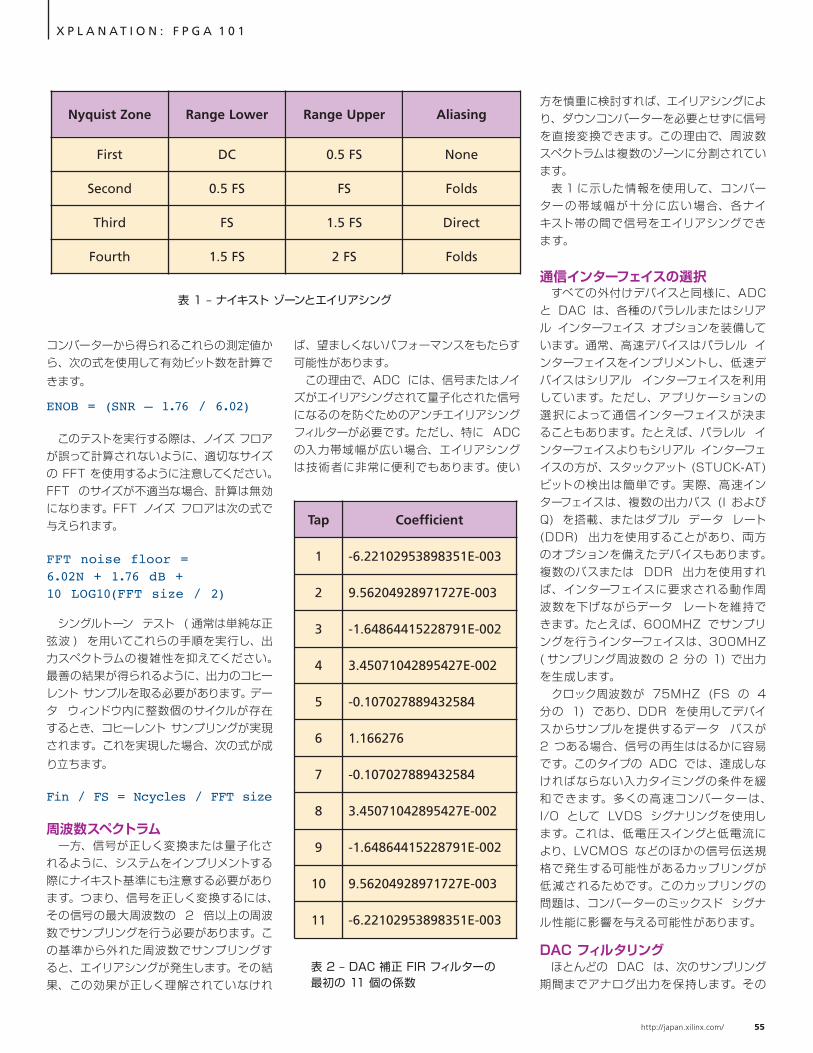
方を慎重に検討すれば、エイリアシングにより、ダウンコンバーターを必要とせずに信号を直接変換できます。この理由で、周波数スペクトラムは複数のゾーンに分割されています。 表 1 に示した情報を使用して、コンバーターの帯域幅が十分に広い場合、各ナイキスト帯の間で信号をエイリアシングできます。
通信インターフェイスの選択 すべての外付けデバイスと同様に、ADC と DAC は、各種のパラレルまたはシリアル インターフェイス オプションを装備しています。通常、高速デバイスはパラレル インターフェイスをインプリメントし、低速デバイスはシリアル インターフェイスを利用しています。ただし、アプリケーションの選択によって通信インターフェイスが決まることもあります。たとえば、パラレル インターフェイスよりもシリアル インターフェイスの方が、スタックアット (STUCK-AT) ビットの検出は簡単です。実際、高速インターフェイスは、複数の出力バス (I および Q) を搭載、またはダブル データ レート (DDR) 出力を使用することがあり、両方のオプションを備えたデバイスもあります。複数のバスまたは DDR 出力を使用すれば、インターフェイスに要求される動作周波数を下げながらデータ レートを維持できます。たとえば、600MHZ でサンプリングを行うインターフェイスは、300MHZ ( サンプリング周波数の 2 分の 1) で出力を生成します。 クロック周波数が 75MHZ (FS の 4 分の 1) であり、DDR を使用してデバイスからサンプルを提供するデータ バスが 2 つある場合、信号の再生ははるかに容易です。このタイプの ADC では、達成しなければならない入力タイミングの条件を緩和できます。多くの高速コンバーターは、I/O として LVDS シグナリングを使用します。これは、低電圧スイングと低電流により、LVCMOS などのほかの信号伝送規格で発生する可能性があるカップリングが低減されるためです。このカップリングの問題は、コンバーターのミックスド シグナル性能に影響を与える可能性があります。
DAC フィルタリング ほとんどの DAC は、次のサンプリング期間までアナログ出力を保持します。その
コンバーターから得られるこれらの測定値から、次の式を使用して有効ビット数を計算できます。
ENOB = (SNR – 1.76 / 6.02)
このテストを実行する際は、ノイズ フロアが誤って計算されないように、適切なサイズの FFT を使用するように注意してください。FFT のサイズが不適当な場合、計算は無効になります。FFT ノイズ フロアは次の式で与えられます。
FFT noise floor = 6.02N + 1.76 dB + 10 LOG10(FFT size / 2)
シングルトーン テスト ( 通常は単純な正弦波 ) を用いてこれらの手順を実行し、出力スペクトラムの複雑性を抑えてください。最善の結果が得られるように、出力のコヒーレント サンプルを取る必要があります。データ ウィンドウ内に整数個のサイクルが存在するとき、コヒーレント サンプリングが実現されます。これを実現した場合、次の式が成り立ちます。
Fin / FS = Ncycles / FFT size
周波数スペクトラム 一方、信号が正しく変換または量子化されるように、システムをインプリメントする際にナイキスト基準にも注意する必要があります。つまり、信号を正しく変換するには、その信号の最大周波数の 2 倍以上の周波数でサンプリングを行う必要があります。この基準から外れた周波数でサンプリングすると、エイリアシングが発生します。その結果、この効果が正しく理解されていなけれ
X P L A N A T I O N : F P G A 1 0 1
ば、望ましくないパフォーマンスをもたらす可能性があります。 この理由で、ADC には、信号またはノイズがエイリアシングされて量子化された信号になるのを防ぐためのアンチエイリアシング フィルターが必要です。ただし、特に ADC の入力帯域幅が広い場合、エイリアシングは技術者に非常に便利でもあります。使い
Nyquist Zone Range Lower Range Upper Aliasing
First DC 0.5 FS None
Second 0.5 FS FS Folds
Third FS 1.5 FS Direct
Fourth 1.5 FS 2 FS Folds
Tap Coefficient
1 -6.22102953898351E-003
2 9.56204928971727E-003
3 -1.64864415228791E-002
4 3.45071042895427E-002
5 -0.107027889432584
6 1.166276
7 -0.107027889432584
8 3.45071042895427E-002
9 -1.64864415228791E-002
10 9.56204928971727E-003
11 -6.22102953898351E-003
表 1 – ナイキスト ゾーンとエイリアシング
表 2 – DAC 補正 FIR フィルターの最初の 11 個の係数
http://japan.xilinx.com/ 55
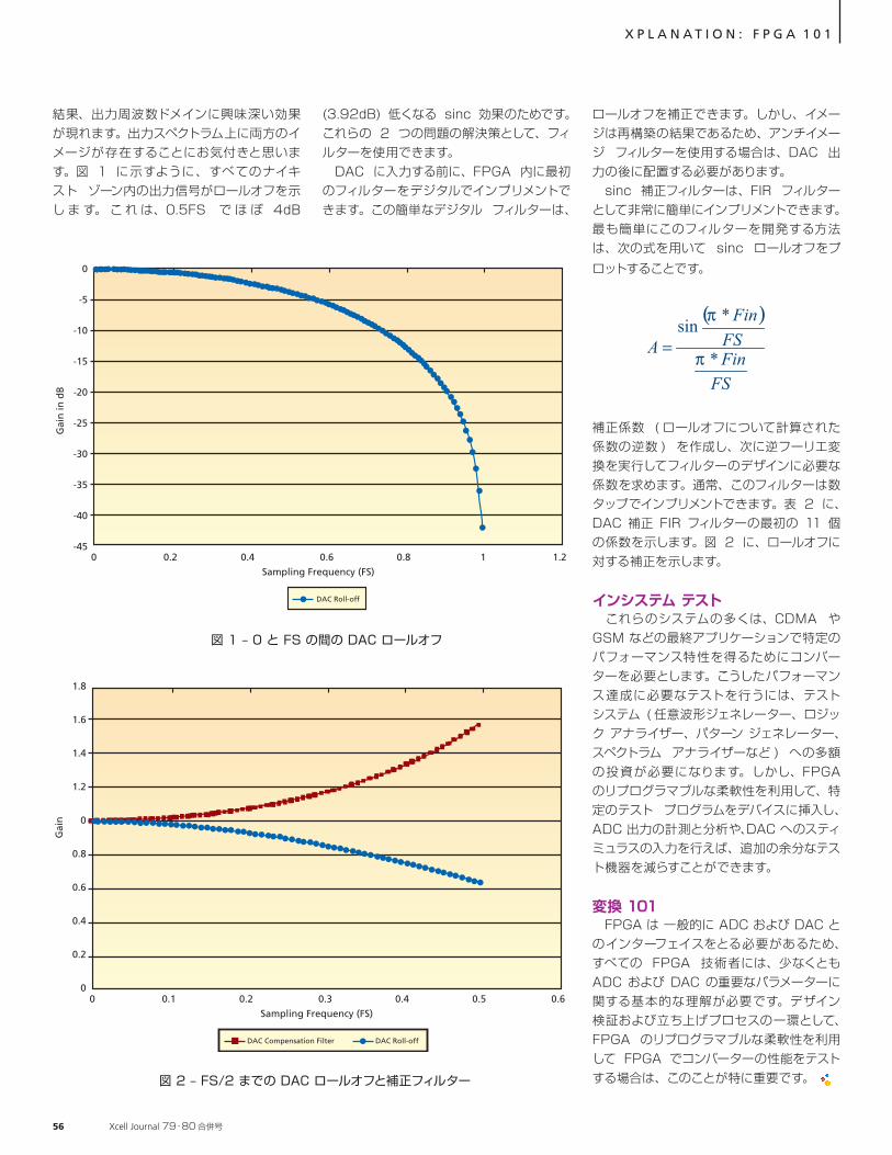
X P L A N A T I O N : F P G A 1 0 1
結果、出力周波数ドメインに興味深い効果が現れます。出力スペクトラム上に両方のイメージが存在することにお気付きと思います。図 1 に示すように、すべてのナイキスト ゾーン内の出力信号がロールオフを示し ま す。 こ れ は、0.5FS で ほ ぼ 4dB
(3.92dB) 低くなる sinc 効果のためです。これらの 2 つの問題の解決策として、フィルターを使用できます。 DAC に入力する前に、FPGA 内に最初のフィルターをデジタルでインプリメントできます。この簡単なデジタル フィルターは、
ロールオフを補正できます。しかし、イメージは再構築の結果であるため、アンチイメージ フィルターを使用する場合は、DAC 出力の後に配置する必要があります。 sinc 補正フィルターは、FIR フィルターとして非常に簡単にインプリメントできます。最も簡単にこのフィルターを開発する方法は、次の式を用いて sinc ロールオフをプロットすることです。
補正係数 ( ロールオフについて計算された係数の逆数 ) を作成し、次に逆フーリエ変換を実行してフィルターのデザインに必要な係数を求めます。通常、このフィルターは数タップでインプリメントできます。表 2 に、DAC 補正 FIR フィルターの最初の 11 個の係数を示します。図 2 に、ロールオフに対する補正を示します。
インシステム テスト これらのシステムの多くは、CDMA や GSM などの最終アプリケーションで特定のパフォーマンス特性を得るためにコンバーターを必要とします。こうしたパフォーマンス達成に必要なテストを行うには、テスト システム ( 任意波形ジェネレーター、ロジック アナライザー、パターン ジェネレーター、スペクトラム アナライザーなど ) への多額の投資が必要になります。しかし、FPGA のリプログラマブルな柔軟性を利用して、特定のテスト プログラムをデバイスに挿入し、ADC 出力の計測と分析や、DAC へのスティミュラスの入力を行えば、追加の余分なテスト機器を減らすことができます。
変換 101 FPGA は 一般的に ADC および DAC とのインターフェイスをとる必要があるため、すべての FPGA 技術者には、少なくとも ADC および DAC の重要なパラメーターに関する基本的な理解が必要です。デザイン検証および立ち上げプロセスの一環として、FPGA のリプログラマブルな柔軟性を利用して FPGA でコンバーターの性能をテストする場合は、このことが特に重要です。
Sampling Frequency (FS)
Gai
n in
dB
DAC Roll-off
0
-5
-10
-15
-20
-25
-30
-35
-40
-450 0.2 0.4 0.6 0.8 1 1.2
Sampling Frequency (FS)
DAC Roll-offDAC Compensation Filter
1.8
1.6
1.4
1.2
0
0.8
0.6
0.4
0.2
00 0.1 0.2 0.3 0.4 0.5 0.6
Gai
n
図 1 – 0 と FS の間の DAC ロールオフ
図 2 – FS/2 までの DAC ロールオフと補正フィルター
56 Xcell Journal 79・80 合併号
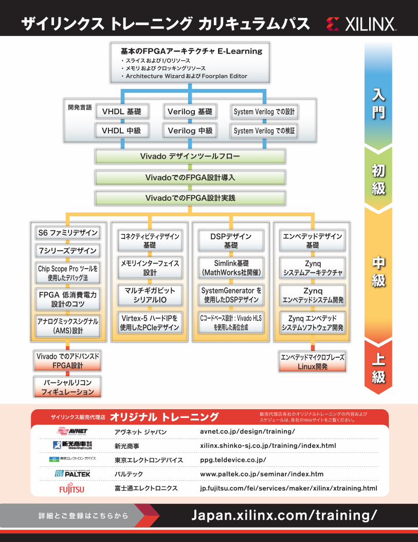
基本のFPGAアーキテクチャ E-Learning・ スライスおよび I/Oリソース・ メモリおよびクロッキングリソース・ Architecture WizardおよびFoorplan Editor
VHDL 基礎
VHDL 中級
Verilog 基礎 System Verilog での設計
Verilog 中級
Vivado デザインツールフロー
VivadoでのFPGA設計導入
開発言語
コネクティビティデザイン基礎
アヴネット ジャパン
新光商事
東京エレクトロンデバイス
パルテック
富士通エレクトロニクス
avnet.co.jp/design/training/
xilinx.shinko-sj.co.jp/training/index.html
ppg.teldevice.co.jp/
www.paltek.co.jp/seminar/index.htm
jp.fujitsu.com/fei/services/maker/xilinx/xtraining.html
詳細とご登録はこちらから Japan.xilinx.com/training/
System Verilog での検証
VivadoでのFPGA設計実践
S6 ファミリデザイン
7シリーズデザイン
Chip Scope Pro ツールを使用したデバッグ法
FPGA 低消費電力設計のコツ
アナログミックスシグナル(AMS)設計
メモリインターフェイス設計
Virtex-5 ハードIPを使用したPCIeデザイン
マルチギガビットシリアルIO
Simlink基礎(MathWorks社開催)
Cコードベース設計 : Vivado HLSを使用した高位合成
SystemGenerator を使用したDSPデザイン
DSPデザイン基礎
Zynqシステムアーキテクチャ
Zynq エンベデッドシステムソフトウェア開発
Zynqエンベデッドシステム開発
エンベデッドデザイン基礎
Vivado でのアドバンスドFPGA設計
パーシャルリコンフィギュレーション
エンベデッドマイクロブレーズLinux開発
過去 10 年間、私たちはクラウド コンピューティングの新たなグローバル市場の出現を目の当たりにしてきました。インターネット経由のサービスとしてコンピューティングを提供するこの新しいパラダイムは、コンピューターの使い方の根本的な転換を表すものです。クラウドは、企業が自社のローカル IT インフラストラクチャから、最適化されたリモート コンピューティング クラスターに ( つまり、クラウド サービスを提供する事業者のシステムに ) タスクを移転する手段を提供します。一方消費者は、クラウドによって、統一された方法で世界のあ
XPERT OPINION
FPGAs Head for the Cloud
by Michaela BlottSenior Research EngineerXilinx, [email protected]
Tom EnglishResearch ScientistXilinx, [email protected]
Emilio BilliCTOEB [email protected]
FPGA の応用クラウドを 加速化
58 Xcell Journal 79・80 合併号
らゆる場所から各種のコンピューティング機器の助けを借りて、ストレージ、ビデオ、メッセージング、ソーシャル ネットワーキング、ゲーム、Web 検索などの多様なサービスを利用できます。 クラウド コンピューティング革命の中核にあるのは、世界中のユーザーへのサービス提供に必要な計算処理能力、ストレージ、インターコネクトを統合したデータセンターです。データセンターは驚くべき成長を経験しており、それは多額の投資に結びついています。Synergy Research Group によると、データセンターのネットワーク イ
ンフラストラクチャの売上は 2010 年だけで 22% も伸びています。クラウド コンピ ュ ー ティン グ 革 命 の 最 前 線 に 立 つ
Google 社や Facebook 社などの企業は、世界中の多数のユーザーに対応す
るための巨大なデータセンター インフラストラクチャの必要性を正
しく予測していました。
FPGA の利点 データセンター の高速化、大規模化、低コスト化、省エネルギー化への要求が高まるにつれて、FPGA テクノロジはコンピューティング、ストレージ、ネットワーキングに数え切れないほどのメリットをもたらします。ネットワーク インフラストラクチャに FPGA
を組み込めば、高い電力効率を維持しながら、ます
ます増大するスループットと処理能力への要求に対応でき
ます。さらに、新たな通信プロトコ ルが 次々と 登 場 する ネット
ワーク環境下では、FPGA の本質的な柔軟性が重要なメリットにな
ります。 FPGA は基本的レベルで、
適切な物理的インターフェイスと、高速メモリ インター
フェイスに必要なサポートおよび 帯域 幅を提 供
しま す。また FPGA は、100G を超えるパ
ケット処理パイプラインをインプリメントできるデバ
イスの 多様 性を提 供します。さらに、 FPGA の高い柔軟性を利用すれば、最大限の効率で動作する高度に最適化されたカスタム回路をインプリメントできます。 データセンター市場における FPGA の最大の問題点は、プログラミング フローの抽象化レベルが低いことですが、AutoESL に見られるような高位合成機能の大幅な改善が、この問題の解決に役立っています。最終的には、基本的ネットワーク機能をカバーするベーシックな FPGA IP ポートフォリオは形成されています。ただし、データ
センター ブリッジング (DCB)、VXLAN、仮想スイッチングなどの専門的テクノロジについては、さらにデータセンター固有のソリューションの開発が待たれています。 サーバーに FPGA を組み込めば、ネットワーク インターフェイス カード (NIC) 用デバイスとして魅力を発揮します。Intel 社やBroadcom 社など各社からイーサネットおよびファイバー チャネル用標準アダプターのインプリメント用に多くのコントローラーが 提 供されていますが、ネットワークと CPU 間のデータ パス上に追加のプロセッシング機能を統合する場合は、FPGA が理想的です。追加のプロセッシング機能の例として、暗号化、高頻度トレーディング、TCP オフロード エンジン (TOE) などが挙げられます。 ネットワーク インターフェイスまたはプロセッシング機能をカスタマイズする必要がある場合にも、FPGA は魅力的なオプションとなります。こうしたシナリオでは、FPGA は、高速シリアル トランシーバー、メモリ インターフェイス、PCIe® エンドポイントを提供します。また基本 IP ブロックと組み合わせて、高スループットのデータ ストリーム プロセッシングに対応する大型ファブリックを実現できます。この市場の特定のニーズに対応する、より高度な IP/ ソリューションのポートフォリオが揃えば、通常はエンド ユーザーが完全に統合されたプラットフォームの導入に慣れている環境では、FPGA が競争力を発揮できるはずです。たとえば、数千の同時セッションに対応する高度な TOE IP ブロック ( およびそれに付随して完全な Linux ドライバーと TCP/IP スタック ) が提供されれば、さまざまな新しい FPGA データセンター アプリケーションの可能性が開かれそうです。 このようなネットワーク アダプターの特殊な例として、QuickPath Interconnect (QPI) ネットワーク アダプターが挙げられます。QPI は、Intel 社独自の高帯域幅、低レイテンシの CPU インターコネクトです。ザイリンクスは、QPI によって FPGA と CPU を直接接続できる IP を開発しました。この IP は、ホスト インターフェイス上のレイテンシを大幅に低減し、CPU とネットワーク インターフェイス間に高帯域幅を提供します。すでに高度に並列化されているアプリケーションでは、レイテンシが性能上の主要なボトルネックになりつつあるため、データセンター内でこのようなネット
X P E R T O P I N I O N
データセンターの急成長が既存および先進の FPGA デバイスに新たな機会を開く
http://japan.xilinx.com/ 59
ワーク アダプターは非常に魅力的です。QPI NIC とホスト間の双方向ピーク帯域幅は、標準的な PCIe Gen2 サーバー NIC の 4 倍に達します。QPI は、高い転送速度、FPGA/CPU 間の直接転送、短いヘッダーを利用して、PCIe よりはるかに短いレイテンシで小さなメッセージを転送できます。すでに高度に並列化されているアプリケーションで、レイテンシが性能上の主要なボトルネックになるにつれて、超低レイテンシ、高帯域幅の QPI NIC は非常に魅力的な提案となります。 マザーボード上の FPGA マザーボード上に搭載される FPGA には、さらに多くのアプリケーションが考えられます。インメモリ キャッシュなど、データセンターの一般的なアプリケーションには、特に x86 系プロセッサが最適というわけではないにもかかわらず、現在 x86 ベースのサーバー上にインプリメントされているものがあります。このようなアプリケーションでは、FPGA によってパフォーマンス、消費電力、およびレイテンシが飛躍的に向上する可能性があります。コンピューティングのトレンドは、分散された多数のコアから、パイプ
ライン方式のデータ処理へと移行していますが、この手法には FPGA アーキテクチャが有利です。シリコン チップのボリュームも、FPGA のアプリケーションに最適と言えます。ただし、Facebook 社などのエンド ユーザー向けに x86 ベース サーバー上の C コンパイラと競い合うには、FPGA プログラミング ツールの低い抽象化レベルを改善する必要がありそうです。 さらに将来的な展望として、非公式に「非
力なノード (wimpy node)」と呼ばれるデータセンター内のサブクラス サーバーが挙げられます。ザイリンクスは、この市場の最新のサーバー アーキテクチャおよび SoC アーキテクチャに対応する主要テクノロジの多くをすでに保有しています。これには、ARM プロセッサ コア、PCIe インターフェイス ブロック、メモリ インターフェイス、およびプログラマブル ロジックなどがあります。現在の Zynq ™ -7000 All Programmable SoC は、Applied Micro 社の X-Gene のような「非力なノード」市場向けの ARM ベースのサーバー SoC と競い合うにはまだ機能が不十分ですが、すでに利用可能なテクノロジ ブロックを使用して、将来の Zynq デバイスをデータセンター サーバーに搭載してその威力を発揮できそうです。 最後に、特にハイパフォーマンス コンピューティング分野における処理需要の増大に対して、FPGA と CPU を組み合わせたハイブリッド ソリューションが大きく貢献する可能性があります。Convey 社と Maxeler 社の既存ソリューションは、このようなアプローチがもたらす性能面および消費電力面の大きなメリットを紹介するも
のです。たとえば、Maxeler 社が金融業界の顧客向けに開発したクレジット デリバティブ価 格 評 価システムは、インテル ® Xeon® プロセッサ E5430 搭載サーバー上で動作するソフトウェアに比べて、処理速度を最大 37 倍に向上し、消費電力を 97% 以上削減しています。QPI テクノロジにより、低レイテンシ、高帯域幅のキャッシュ コヒーレント インターフェイスを介してハードウェア アクセラレータと CPU が
より緊密に結合されるにつれて、上記のメリットはさらに拡大する可能性があります。
データ ストレージ、データ ウェアハウス、データ分析 既存の FPGA は、サーバーおよびネットワーキング市場と同様に、ストレージ、データ ウェアハウス、およびデータ分析市場でも、3 つのまったく異なる方法で、競争力のあるインプリメンテーションを提供します。まず第 1 に、最近のトレンドでは、フラッシュ ベースのストレージをホストの近くに装備します。一群の新しい PCIe SSD コントローラーが、フラッシュと PCIe の直接接続を可能にします。FPGA はすでにこの市場に参入し、主要な機能と基本的な IP ビルディング ブロックを提供しています。 さらに重要なメリットは、FPGA の高い柔軟性です。現在、Open NAND Flash インターフェイス (ONFi) などの新しい標準化作業が進められてはいますが、フラッシュ ベースのインターフェイスの業界標準規格はまだ確立されていません。 この市場でも、FPGA は、クエリー処理、フィルタリングの処理、一部の関係演算子の伸張と実行の高速化に貢献します。スルー
プットのボトルネックに対処するためにインテリジェント機能の強化が必要になる将来のストレージ アプライアンスでは、この機能が非常に重要になりそうです。最後に、FPGA は、多くの CPU サイクルを消費するファイル システム操作を高速化できるので、いわゆる「スーパー ストレージ」アプリケーションに重要な役割を果たします。これらのアプリケーションは、現在、ストレージ エリア ネットワーク内にストレージ サー
X P E R T O P I N I O N
Hybrid Computing
Desktop Virtualization
OPST
Optical Backhaul
Custom NICs
Smart Analytics
Super Storage
Smart NICs
Flash Controllers
Group 1 Group 2 Group 3
QPI NIC
QPI I/O & Memory Expansion
Application-specific Servers
Cloud RAN
Smart Networking
Wimpy Nodes
Optical Interconnects
図 1 – データセンターでは、3 つの幅広いカテゴリに分類されるアプリケーションが FPGA によるインプリメンテーションを待ち望んでいる
60 Xcell Journal 79・80 合併号
バーとともに配置される別個のサーバー上で動作しています。FPGA を使用した高速化により、ストレージ サーバーに対する制御サーバーの比率を低減し、利用可能なストレージ容量と性能を拡張できそうです。 既存の FPGA テクノロジは、これらの要件に対応できます。特に、現在の Zynq アーキテクチャのエンベデッド ARM プロセッサは、すでに OS 機能を採り入れています。もちろん、より高度な IP ソリューションのポートフォリオが揃えば、FPGA のポテンシャルはさらに向上し、新しいデザインの開発を迅速化できます。
3 種類のアプリケーション 図 1 に示すように、筆者らは、FPGA の多彩なアプリケーションを 3 つのグループに分類しています。第 1 のグループには、追加の開発作業を必要としないアプリケーションが含まれます。シリコン機能、IP ポートフォリオ、関連ソフトウェア、およびプログラマビリティは、これらのデータセンター市場に十分に対応可能であり、一部の用途ではすでに FPGA が採用されています。たとえば、Intune Networks 社は FPGA を使用して光パケット スイッチ / トランスポート (OPST) ソリューションをインプリメントし、消費電力について最大 300% のコスト削減を発表しています。Maxeler 社と Convey Computers 社は FPGA ベースのハイブリッド コンピューティング ソリューションを提 供しています。IBM/Netezza 社は Smart Analytic 製品に FPGA を搭載しています。BlueArc 社は FPGA によるスーパー ストレージの大幅な向上の実例を示しています。FusionIO 社はフラッシュ コントローラーに FPGA を使用しています。Napatech 社と Nallatech 社を含む多数のベンダーは、FPGA ベースのスマート NIC やカスタム NIC を提供しています。 第 2 のグループには、多少高度な開発作業を必要とするアプリケーションが含まれます。このカテゴリで最も注目すべきなのは QPI に関連するアプリケーション、すなわち QPI NIC とメモリおよび I/O 拡張です。 第 3 の最終グループには、シリコン機能またはプログラミング環境に関する多くの研究開発活動を必要とする長期的に期待できるものが含まれます。たとえば、FPGA デバイスを使用して「非力なノード (wimpy node)」を構築するには、64 ビット ARM
プロセッサのインテグレーションの強化とメモリ インターフェイスの広帯域化、高速化を実現した、新世代の Zynq デバイスが必要になります。 ア プ リケー ション 固 有 の サ ーバー と C-RAN ( クラウド RAN) は、グループ 2 とグループ 3 の境界線上にあります。いずれも必要なインフラストラクチャとプラットフォームを提供するために高度な開発作業が必要であり、抽象化レベルの高い新しいプログラミング ツールの恩恵を受けるはずです。ただし、一部のエンド ユーザーには従来の RTL ベースのデザイン フローで十分であるため、これらのアプリケーションは第 2 のグループに移すことができます。
非常にダイナミックな市場 データセンターは、インターフェイスの規格とプロトコルが急速に進化していく非常にダイナミックな市場です。特にネットワーク機器市場で、またコンピューティング 機 能 市 場 に つ い て も、 こ の 環 境 は FPGA ベースの高速プロセッシング システムを導入する素晴らしい機会をもたらします。Kintex ™ ファミリ デバイスおよび Virtex® ファミリ デバイスがその高速シリアル I/O とそれに対応する IP コアを利用するなど、ザイリンクスの最新テクノロジを使用した FPGA インプリメンテーションは、こうしたアプリケーションに最適と言えます。 データセンター市場のニーズを見極めることで、FPGA のアプリケーションはさらに広がります。データセンターのアプリケーションの大半は、検索やソートの対象となる大量のデータを扱います。このため、特にメモリ アクセス機能 ( アクセスの帯域幅と密度 ) と ( シリコンまたは IP コアの形式での ) ハッシュ法および検索機能のサポートは極めて重要です。ザイリンクスのスタックド シリコン インターコネクト (SSI) テ クノ ロ ジ を 採 用 し た 将 来 の FPGA デバイスは、この分野で重要な役割を果たす可能性があります。 最後に、これらの機会、特にサーバー市場における機会が実現されるかどうかは、FPGA のプログラマビリティの向上にかかっています。FPGA のプログラミングは、データセンターのプログラマに受け入れられるレベルまで抽象化される必要があります。
X P E R T O P I N I O N
Get on Target
パートナの皆様御社の製品・サービスをXcell journal 誌上でPR してみませんか?
Xcell Journal はプログラマブル ロジック ユーザーへ
ザイリンクス製品/ツールの最新情報をはじめシステム/アプリケーションの解説、
サービス/サポート情報、サードパーティ各社のツール情報などをお届けしています。
現在では日本各地の 10,000 名を超える幅広い分野のエンジニアの皆様に愛読いただいておりザイリンクスの HP から、無償でダウンロードまたは iPad 対応デジタル版が購読できます。貴社製品/ソリューションのプロモーションに
非常に効果的なメディアです。
広告掲載に関するお問い合わせ先Xcell Journal 日本語版への広告出向に関するお問い合せは
E-mail にてご連絡下さい。 有限会社 エイ・シー・シー[email protected]
http://japan.xilinx.com/ 61
ハードウェア、ソフトウェア、I/O がプログラマブルなSoC
■東京エレクトロン デバイス(株) TEL(045)443-4016 [email protected] ■アヴネット ジャパン(株) TEL(03)5792-8210 [email protected] ■(株)PALTEK TEL(045)477-2005 [email protected]■富士通エレクトロニクス(株) TEL(045)415-5825 [email protected] ■新光商事(株) TEL(03)6361-8086 X-Pro@shinko-sj.co.jp©Copyright 2013 Xilinx, Inc. All rights reserved. ザイリンクスの名称およびロゴは、米国およびその他各国のザイリンクス社の登録商標および商標です。ARMは、EUおよびその他の国におけるARM Limitedの登録商標です。他のすべての商標はそれぞれの所有者の財産です。
詳細はこちら