Embed Size (px)
Citation preview
SPECIFICATIONS
PCIe-577512-Bit, 6.4 GS/s, 2-Channel PCI FlexRIO Digitizer Device
This document lists the specifications for the PCIe-5775. Specifications are subject to changewithout notice. For the most recent device specifications, refer to ni.com/support.
Note These specifications are typical at 25 °C unless otherwise noted.
ContentsDefinitions.................................................................................................................................1Digital I/O................................................................................................................................. 2
Digital I/O Single-Ended Channels...................................................................................2Digital I/O High-Speed Serial MGT.................................................................................3
Reconfigurable FPGA...............................................................................................................4Onboard DRAM........................................................................................................................4Analog Input............................................................................................................................. 5
General Characteristics..................................................................................................... 5Typical Specifications....................................................................................................... 5
REF/CLK IN........................................................................................................................... 10General Characteristics................................................................................................... 10
Bus Interface........................................................................................................................... 12Maximum Power Requirements..............................................................................................12Physical................................................................................................................................... 13Environment............................................................................................................................13
Operating Environment...................................................................................................13Storage Environment.......................................................................................................13
DefinitionsWarranted specifications describe the performance of a model under stated operatingconditions and are covered by the model warranty.
Characteristics describe values that are relevant to the use of the model under stated operatingconditions but are not covered by the model warranty.• Typical specifications describe the performance met by a majority of models.• Nominal specifications describe an attribute that is based on design, conformance testing,
or supplemental testing.
Specifications are Typical unless otherwise noted.
Digital I/OConnector Molex™ Nano-Pitch I/O™
5.0 V Power ±5%, 50 mA maximum, nominal
Table 1. Digital I/O Signal Characteristics
Signal Type Direction
MGT Tx± <0..3>1 Xilinx UltraScale GTH Output
MGT Rx± <0..3>1 Xilinx UltraScale GTH Input
DIO <0..7> Single-ended Bidirectional
5.0 V DC Output
GND Ground —
Digital I/O Single-Ended ChannelsNumber of channels 8
Signal type Single-ended
Voltage families 3.3 V, 2.5 V, 1.8 V, 1.5 V, 1.2 V
Input impedance 100 kΩ, nominal
Output impedance 50 Ω, nominal
Direction control Per channel
Minimum required direction changelatency
200 ns
Maximum output toggle rate 60 MHz with 100 μA load, nominal
1 Multi-gigabit transceiver (MGT) signals are available on devices with KU040 and KU060 FPGAsonly.
2 | ni.com | PCIe-5775 Specifications

Table 2. Digital I/O Single-Ended DC Signal Characteristics2
Voltage Family VIL VIH VOL
(100µA load)VOH
(100µA load)Maximum DC Drive
Strength
3.3 V 0.8 V 2.0 V 0.2 V 3.0 V 24 mA
2.5 V 0.7 V 1.6 V 0.2 V 2.2 V 18 mA
1.8 V 0.62 V 1.29 V 0.2 V 1.5 V 16 mA
1.5 V 0.51 V 1.07 V 0.2 V 1.2 V 12 mA
1.2 V 0.42 V 0.87 V 0.2 V 0.9 V 6 mA
Digital I/O High-Speed Serial MGT3
Note MGTs are available on devices with KU040 and KU060 FPGAs only.
Data rate 500 Mbps to 16.375 Gbps, nominal
Number of Tx channels 4
Number of Rx channels 4
I/O AC coupling capacitor 100 nF
MGT TX± ChannelsMinimum differential output voltage4 170 mV pk-pk into 100 Ω, nominal
I/O coupling AC-coupled with 100 nF capacitor
MGT RX± ChannelsDifferential input voltage range
≤ 6.6 Gb/s 150 mV pk-pk to 2000 mV pk-pk, nominal
> 6.6 Gb/s 150 mV pk-pk to 1250 mV pk-pk, nominal
Differential input resistance 100 Ω, nominal
I/O coupling DC-coupled, requires external capacitor
2 Voltage levels are guaranteed by design through the digital buffer specifications.3 For detailed FPGA and High-Speed Serial Link specifications, refer to Xilinx documentation.4 800 mV pk-pk when transmitter output swing is set to the maximum setting.
PCIe-5775 Specifications | © National Instruments | 3
Reconfigurable FPGAPCIe-5775 modules are available with multiple FPGA options. The following table lists theFPGA specifications for the PCIe-5775 FPGA options.
Table 3. Reconfigurable FPGA Options
KU035 KU040 KU060
LUTs 203,128 242,200 331,680
DSP48 slices(25 × 18 multiplier)
1,700 1,920 2,760
Embedded Block RAM 19.0 Mb 21.1 Mb 38.0 Mb
Data Clock Domain 200 MHz, 16 samples per cycle per channel (dual channel mode),32 samples per cycle (single channel mode)
Timebase referencesources
Onboard 100 MHz oscillator
Data transfers DMA, interrupts,programmed I/O
DMA, interrupts, programmed I/O,multi-gigabit transceivers
Number of DMAchannels
60
Note The Reconfigurable FPGA Options table depicts the total number of FPGAresources available on the part. The number of resources available to the user isslightly lower, as some FPGA resources are consumed by board-interfacing IP forPCI Express, device configuration, and various board I/O. For more information,contact NI support.
Onboard DRAMMemory size 4 GB (2 banks of 2 GB)
DRAM clock rate 1064 MHz
Physical bus width 32 bit
LabVIEW FPGA DRAM clock rate 267 MHz
LabVIEW FPGA DRAM bus width 256 bit per bank
Maximum theoretical data rate 17 GB/s (8.5 GB/s per bank)
4 | ni.com | PCIe-5775 Specifications
Analog Input
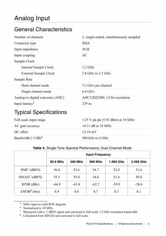
General CharacteristicsNumber of channels 2, single-ended, simultaneously sampled
Connector type SMA
Input impedance 50 Ω
Input coupling ACSample Clock
Internal Sample Clock 3.2 GHz
External Sample Clock 2.8 GHz to 3.2 GHz
Sample Rate
Dual channel mode 3.2 GS/s per channel
Single channel mode 6.4 GS/s
Analog-to-digital converter (ADC) ADC12DJ3200, 12-bit resolution
Input latency5 239 ns
Typical SpecificationsFull-scale input range 1.25 V pk-pk (5.92 dBm) at 10 MHz
AC gain accuracy ±0.11 dB at 10 MHz
DC offset ±2.19 mV
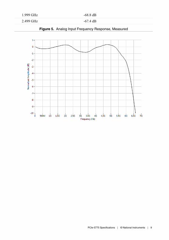
Bandwidth (-3 dB)6 500 kHz to 6 GHz
Table 4. Single-Tone Spectral Performance, Dual Channel Mode
Input Frequency
99.9 MHz 399 MHz 999 MHz 1.999 GHz 2.499 GHz
SNR7 (dBFS) 56.0 55.6 54.7 52.9 51.6
SINAD7 (dBFS) 55.5 55.0 54.0 51.8 50.8
SFDR (dBc) -64.9 -63.4 -62.7 -59.9 -58.6
ENOB8 (bits) 8.9 8.8 8.7 8.3 8.1
5 SMA input to LabVIEW diagram6 Normalized to 10 MHz.7 Measured with a -1 dBFS signal and corrected to full-scale. 3.2 kHz resolution bandwidth.8 Calculated from SINAD and corrected to full scale.
PCIe-5775 Specifications | © National Instruments | 5
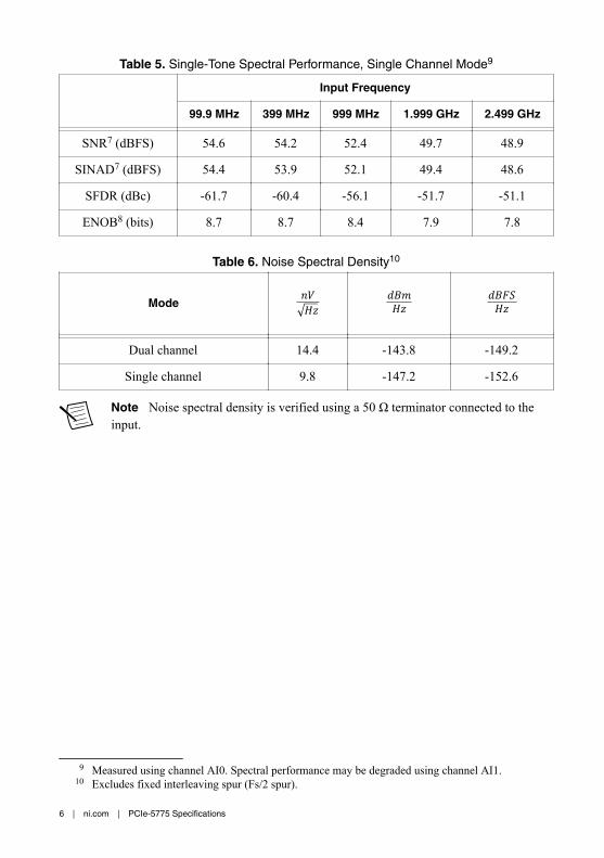
Table 5. Single-Tone Spectral Performance, Single Channel Mode9
Input Frequency
99.9 MHz 399 MHz 999 MHz 1.999 GHz 2.499 GHz
SNR7 (dBFS) 54.6 54.2 52.4 49.7 48.9
SINAD7 (dBFS) 54.4 53.9 52.1 49.4 48.6
SFDR (dBc) -61.7 -60.4 -56.1 -51.7 -51.1
ENOB8 (bits) 8.7 8.7 8.4 7.9 7.8
Table 6. Noise Spectral Density10
ModenVHz dBmHz dBFSHz
Dual channel 14.4 -143.8 -149.2
Single channel 9.8 -147.2 -152.6
Note Noise spectral density is verified using a 50 Ω terminator connected to theinput.
9 Measured using channel AI0. Spectral performance may be degraded using channel AI1.10 Excludes fixed interleaving spur (Fs/2 spur).
6 | ni.com | PCIe-5775 Specifications
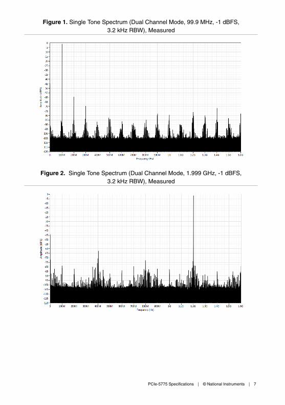
Figure 1. Single Tone Spectrum (Dual Channel Mode, 99.9 MHz, -1 dBFS,3.2 kHz RBW), Measured
Figure 2. Single Tone Spectrum (Dual Channel Mode, 1.999 GHz, -1 dBFS,3.2 kHz RBW), Measured
PCIe-5775 Specifications | © National Instruments | 7
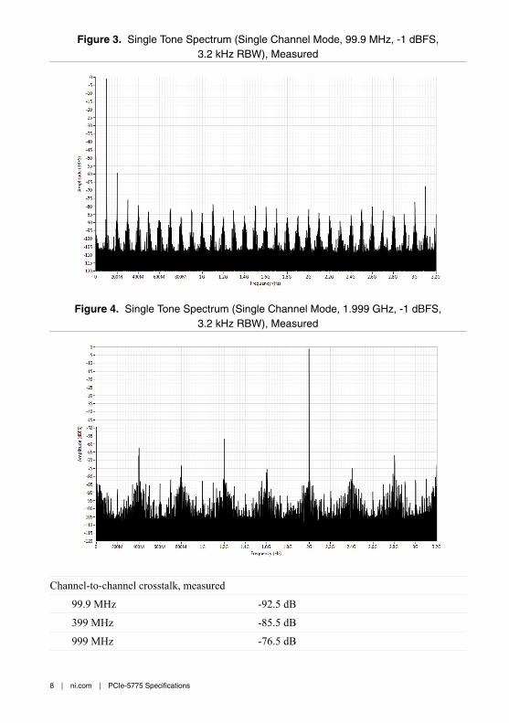
Figure 3. Single Tone Spectrum (Single Channel Mode, 99.9 MHz, -1 dBFS,3.2 kHz RBW), Measured
Figure 4. Single Tone Spectrum (Single Channel Mode, 1.999 GHz, -1 dBFS,3.2 kHz RBW), Measured
Channel-to-channel crosstalk, measured
99.9 MHz -92.5 dB
399 MHz -85.5 dB
999 MHz -76.5 dB
8 | ni.com | PCIe-5775 Specifications
1.999 GHz -68.8 dB
2.499 GHz -67.4 dB
Figure 5. Analog Input Frequency Response, Measured
PCIe-5775 Specifications | © National Instruments | 9
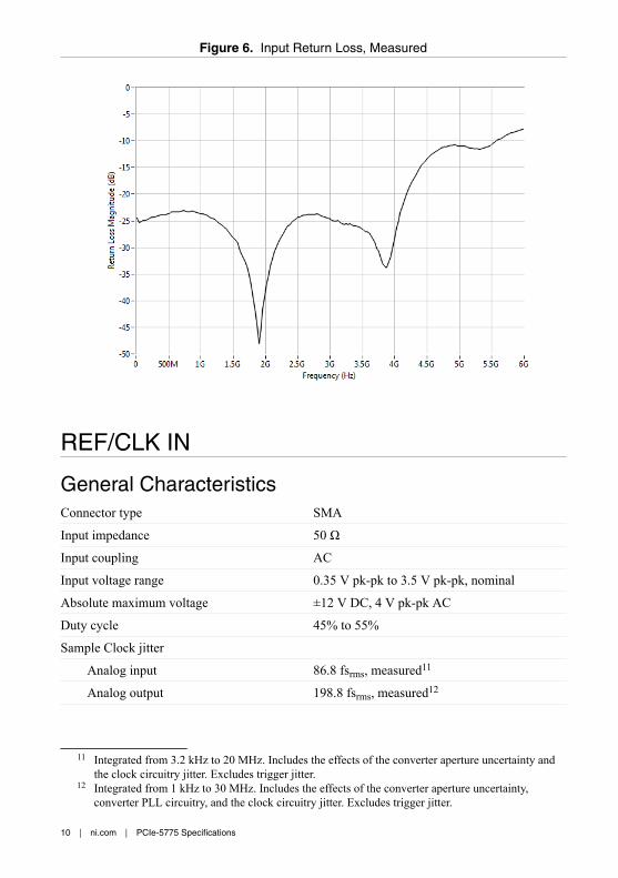
Figure 6. Input Return Loss, Measured
REF/CLK IN
General CharacteristicsConnector type SMA
Input impedance 50 Ω
Input coupling AC
Input voltage range 0.35 V pk-pk to 3.5 V pk-pk, nominal
Absolute maximum voltage ±12 V DC, 4 V pk-pk AC
Duty cycle 45% to 55%
Sample Clock jitter
Analog input 86.8 fsrms, measured11
Analog output 198.8 fsrms, measured12
11 Integrated from 3.2 kHz to 20 MHz. Includes the effects of the converter aperture uncertainty andthe clock circuitry jitter. Excludes trigger jitter.
12 Integrated from 1 kHz to 30 MHz. Includes the effects of the converter aperture uncertainty,converter PLL circuitry, and the clock circuitry jitter. Excludes trigger jitter.
10 | ni.com | PCIe-5775 Specifications

Table 7. Clock Configuration Options
Clock ConfigurationExternal Clock
FrequencyDescription
Internal BaseboardReference Clock13
10 MHz The internal Sample Clock locks tothe 10 MHz Reference Clockprovided from the FPGA baseboard.
External Reference Clock(REF/CLK IN)
10 MHz14 The internal Sample Clock locks to anexternal Reference Clock, which isprovided through the REF/CLK INfront panel connector.
External Sample Clock(REF/CLK IN)
2.8 GHz to 3.2 GHz An external Sample Clock can beprovided through the REF/CLK INfront panel connector.
Figure 7. Analog Input Phase Noise with 800 MHz Input Tone, Measured
13 Default clock configuration.14 The external Reference Clock must be accurate to ±25 ppm.
PCIe-5775 Specifications | © National Instruments | 11
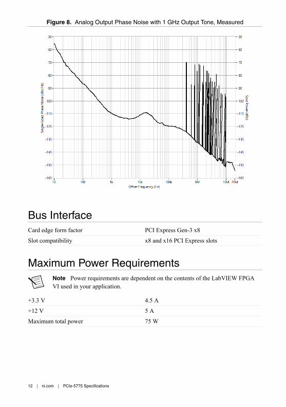
Figure 8. Analog Output Phase Noise with 1 GHz Output Tone, Measured
Bus InterfaceCard edge form factor PCI Express Gen-3 x8
Slot compatibility x8 and x16 PCI Express slots
Maximum Power RequirementsNote Power requirements are dependent on the contents of the LabVIEW FPGAVI used in your application.
+3.3 V 4.5 A
+12 V 5 A
Maximum total power 75 W
12 | ni.com | PCIe-5775 Specifications

PhysicalDimensions (including I/O bracket, notincluding connectors)
12.6 cm × 26.3 cm × 4 cm (5.0 in. × 10.4 in. ×1.6 in.)
Weight 990 g (35 oz)
PCI Express mechanical form factor Standard height, three-quarter length, doubleslot
Integrated air mover (fan) Yes
Maximum rear panel exhaust airflow 84 m3/h (50 CFM) (without any chassisimpedance)
EnvironmentMaximum altitude 2,000 m (800 mbar) (at 25 °C ambient
temperature)
Pollution Degree 2
Indoor use only.
Operating EnvironmentOperating temperature, local15 0 °C to 45 °C
Operating humidity 10% to 90% RH, noncondensing
Storage EnvironmentAmbient temperature range -20 °C to 70 °C
Relative humidity range 5% to 95% RH, noncondensing
15 For PCI Express adapter cards with integrated air movers, NI defines the local operational ambientenvironment to be at the fan inlet. For cards without integrated air movers, NI defines the localoperational ambient environment to be 25 mm (1 in.) upstream of the leading edge of the card.
PCIe-5775 Specifications | © National Instruments | 13

Information is subject to change without notice. Refer to the NI Trademarks and Logo Guidelines at ni.com/trademarks forinformation on NI trademarks. Other product and company names mentioned herein are trademarks or trade names of theirrespective companies. For patents covering NI products/technology, refer to the appropriate location: Help»Patents in yoursoftware, the patents.txt file on your media, or the National Instruments Patent Notice at ni.com/patents. You can findinformation about end-user license agreements (EULAs) and third-party legal notices in the readme file for your NI product. Referto the Export Compliance Information at ni.com/legal/export-compliance for the NI global trade compliance policy and howto obtain relevant HTS codes, ECCNs, and other import/export data. NI MAKES NO EXPRESS OR IMPLIED WARRANTIES ASTO THE ACCURACY OF THE INFORMATION CONTAINED HEREIN AND SHALL NOT BE LIABLE FOR ANY ERRORS. U.S.Government Customers: The data contained in this manual was developed at private expense and is subject to the applicablelimited rights and restricted data rights as set forth in FAR 52.227-14, DFAR 252.227-7014, and DFAR 252.227-7015.
© 2019—2020 National Instruments. All rights reserved.
377961B-01 January 28, 2020